WO2024090232A1 - 異常検出装置 - Google Patents
異常検出装置 Download PDFInfo
- Publication number
- WO2024090232A1 WO2024090232A1 PCT/JP2023/037134 JP2023037134W WO2024090232A1 WO 2024090232 A1 WO2024090232 A1 WO 2024090232A1 JP 2023037134 W JP2023037134 W JP 2023037134W WO 2024090232 A1 WO2024090232 A1 WO 2024090232A1
- Authority
- WO
- WIPO (PCT)
- Prior art keywords
- phase
- arm element
- voltage
- upper arm
- abnormality
- Prior art date
- Legal status (The legal status is an assumption and is not a legal conclusion. Google has not performed a legal analysis and makes no representation as to the accuracy of the status listed.)
- Ceased
Links
Images






Classifications
-
- G—PHYSICS
- G01—MEASURING; TESTING
- G01R—MEASURING ELECTRIC VARIABLES; MEASURING MAGNETIC VARIABLES
- G01R15/00—Details of measuring arrangements of the types provided for in groups G01R17/00 - G01R29/00, G01R33/00 - G01R33/26 or G01R35/00
- G01R15/04—Voltage dividers
-
- G—PHYSICS
- G01—MEASURING; TESTING
- G01R—MEASURING ELECTRIC VARIABLES; MEASURING MAGNETIC VARIABLES
- G01R19/00—Arrangements for measuring currents or voltages or for indicating presence or sign thereof
- G01R19/0084—Measuring voltage only
-
- G—PHYSICS
- G01—MEASURING; TESTING
- G01R—MEASURING ELECTRIC VARIABLES; MEASURING MAGNETIC VARIABLES
- G01R31/00—Arrangements for testing electric properties; Arrangements for locating electric faults; Arrangements for electrical testing characterised by what is being tested not provided for elsewhere
- G01R31/28—Testing of electronic circuits, e.g. by signal tracer
- G01R31/2832—Specific tests of electronic circuits not provided for elsewhere
- G01R31/2836—Fault-finding or characterising
- G01R31/2839—Fault-finding or characterising using signal generators, power supplies or circuit analysers
-
- G—PHYSICS
- G01—MEASURING; TESTING
- G01R—MEASURING ELECTRIC VARIABLES; MEASURING MAGNETIC VARIABLES
- G01R31/00—Arrangements for testing electric properties; Arrangements for locating electric faults; Arrangements for electrical testing characterised by what is being tested not provided for elsewhere
- G01R31/40—Testing power supplies
- G01R31/42—AC power supplies
-
- G—PHYSICS
- G01—MEASURING; TESTING
- G01R—MEASURING ELECTRIC VARIABLES; MEASURING MAGNETIC VARIABLES
- G01R31/00—Arrangements for testing electric properties; Arrangements for locating electric faults; Arrangements for electrical testing characterised by what is being tested not provided for elsewhere
- G01R31/50—Testing of electric apparatus, lines, cables or components for short-circuits, continuity, leakage current or incorrect line connections
- G01R31/52—Testing for short-circuits, leakage current or ground faults
-
- H—ELECTRICITY
- H02—GENERATION; CONVERSION OR DISTRIBUTION OF ELECTRIC POWER
- H02M—APPARATUS FOR CONVERSION BETWEEN AC AND AC, BETWEEN AC AND DC, OR BETWEEN DC AND DC, AND FOR USE WITH MAINS OR SIMILAR POWER SUPPLY SYSTEMS; CONVERSION OF DC OR AC INPUT POWER INTO SURGE OUTPUT POWER; CONTROL OR REGULATION THEREOF
- H02M7/00—Conversion of AC power input into DC power output; Conversion of DC power input into AC power output
- H02M7/42—Conversion of DC power input into AC power output without possibility of reversal
- H02M7/44—Conversion of DC power input into AC power output without possibility of reversal by static converters
- H02M7/48—Conversion of DC power input into AC power output without possibility of reversal by static converters using discharge tubes with control electrode or semiconductor devices with control electrode
-
- H—ELECTRICITY
- H02—GENERATION; CONVERSION OR DISTRIBUTION OF ELECTRIC POWER
- H02P—CONTROL OR REGULATION OF ELECTRIC MOTORS, ELECTRIC GENERATORS OR DYNAMO-ELECTRIC CONVERTERS; CONTROLLING TRANSFORMERS, REACTORS OR CHOKE COILS
- H02P27/00—Arrangements or methods for the control of AC motors characterised by the kind of supply voltage
- H02P27/04—Arrangements or methods for the control of AC motors characterised by the kind of supply voltage using variable-frequency supply voltage, e.g. inverter or converter supply voltage
- H02P27/06—Arrangements or methods for the control of AC motors characterised by the kind of supply voltage using variable-frequency supply voltage, e.g. inverter or converter supply voltage using DC to AC converters or inverters
Definitions
- This disclosure relates to an anomaly detection device.
- the abnormality detection device disclosed in Patent Document 1 has a pull-up resistor and a pull-down resistor connected to the connection point of the upper and lower arms of each phase of the inverter.
- the pull-down resistor of each phase is composed of two voltage-dividing resistors connected in series.
- the judgment unit judges whether the motor relay is stuck on (short circuit failure) or stuck off (open circuit failure) based on the voltage at the voltage-dividing point, which is the connection point of the two voltage-dividing resistors.
- Patent Document 1 In the conventional technology of Patent Document 1, at least the pull-down resistor, out of the pull-up resistor and pull-down resistor for voltage monitoring, is provided inside the drive circuit IC, thereby suppressing an increase in the board mounting area.
- the basic idea is to detect an abnormality by using the voltage of the power supply line stepped down by the pull-up resistor, and the pull-up resistor remains a necessary component regardless of whether it is provided inside the drive circuit IC or mounted on the board.
- Patent Document 1 makes no mention at all of the possibility of eliminating the pull-up resistor.
- the objective of this disclosure is to provide an abnormality detection device that can eliminate the need for a pull-up resistor for a voltage monitor.
- the abnormality detection device disclosed herein includes an inverter, an upper arm element drive circuit, a lower arm element drive circuit, multiple pull-down resistors, and a determination unit.
- the inverter is configured with multiple phase upper and lower arm elements bridge-connected between a power line connected to a battery and a ground line, and converts the battery's DC power and supplies it to each phase winding of a polyphase motor.
- the upper arm element drive circuit outputs a gate signal to the upper arm element.
- the lower arm element drive circuit outputs a gate signal to the lower arm element.
- the multiple pull-down resistors are composed of two voltage-dividing resistors per phase that divide the voltage between the inter-arm connection point, which is the connection point between the upper arm element and the lower arm element of each phase, and ground, and connect the inter-arm connection point to ground.
- the determination unit detects abnormalities in at least the upper arm element and the lower arm element based on the voltage at the voltage-dividing point, which is the connection point of the two voltage-dividing resistors.
- the power supply line and the connection points between the arms of each phase are not connected via pull-up resistors.
- the judgment unit detects ON-stuck abnormalities and OFF-stuck abnormalities of the upper arm element and the lower arm element based on the voltage at the voltage division point when a leak current flows from the upper arm element drive circuit to ground via a pull-down resistor while the upper arm element drive circuit is in operation.
- abnormalities are detected by using the voltage generated when leakage current from the upper arm element drive circuit flows through a pull-down resistor, rather than using the voltage obtained by stepping down the power line voltage using a pull-up resistor.
- Patent Document 1 recognizes leakage current as a drawback, stating that "leakage current from the (upper arm element) drive circuit to the pull-down resistor increases the voltage float, becoming a cause of error.” It also describes cutting leakage current by stopping the operation of the drive circuit when an abnormality is detected in the motor relay as a solution for reducing errors. In contrast, this disclosure takes the opposite approach of actively using leakage current as a voltage source for voltage monitoring, making it possible to eliminate the pull-up resistor.
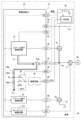
- FIG. 1 is a circuit diagram of an abnormality detection device according to an embodiment
- FIG. 2 is a diagram showing a configuration related to a voltage monitor for one phase, that is, the U phase, in FIG. 1
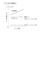
- FIG. 3A is a diagram showing a determination of an upper arm element ON stuck abnormality without leakage cutoff
- FIG. 3B is a diagram showing a determination of an upper arm element ON stuck abnormality in a state in which the operation of the upper arm element drive circuit is stopped (with leakage cut)
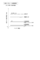
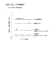
- FIG. 4 is a diagram showing a determination of an upper arm element stuck OFF abnormality.
- FIG. 5 is a diagram showing a determination of a lower arm element ON-fixed abnormality.
- FIG. 6 is a diagram showing a determination of a lower arm element stuck OFF abnormality.
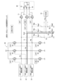
- FIG. 7 is a diagram showing a normal current path during a check for a U-phase motor relay stuck on ON.
- FIG. 8 is a diagram showing a current path when an abnormality occurs during a check for a U-phase motor relay stuck on ON.
- FIG. 9 is a diagram showing a determination of a U-phase motor relay stuck ON abnormality.
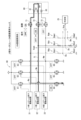
- FIG. 10 is a diagram of a current path under normal conditions when checking for a U-phase motor relay stuck OFF abnormality.
- FIG. 11 is a diagram showing a current path when an abnormality occurs during a check for a U-phase motor relay stuck OFF abnormality.
- FIG. 12 is a diagram showing a determination of a U-phase motor relay stuck-off abnormality.
- the abnormality detection device of this embodiment is applied to a circuit that supplies power to a polyphase motor used as a steering assist motor for an electric power steering device, for example.
- This abnormality detection device detects ON stuck abnormalities (short circuit failures) and OFF stuck abnormalities (open circuit failures) of upper and lower arm elements of an inverter and a motor relay during an initial check of the power supply circuit.
- the ECU of the electric power steering device functions as an abnormality detection device.
- the ECU is composed of a microcomputer, a pre-driver, etc., and is equipped with a CPU, ROM, RAM, I/O, and bus lines connecting these components (not shown).
- the ECU executes software processing by running a pre-stored program in the CPU, and performs control through hardware processing by a dedicated electronic circuit.
- FIG. 1 The configuration of one embodiment is shown in FIG. 1.
- a three-phase motor 80 is used as a "polyphase motor.”
- the three-phase motor 80 will be referred to simply as motor 80.
- ECU 10 which serves as an abnormality detection device, supplies three-phase AC power generated by inverter 60 to three-phase windings 81, 82, and 83 of motor 80.
- the three-phase windings 81, 82, and 83 are connected at neutral point 84.
- the three-phase windings 81, 82, and 83 may also be delta-connected.
- the ECU 10 After the vehicle switch is turned on, the ECU 10 performs an initial check before the motor starts to drive, and detects any abnormalities in the power supply circuit to the motor. If the initial check determines that the power supply circuit to the motor 80 is normal, the ECU 10 controls the drive of the motor 80 so that the motor 80 generates the desired assist torque based on the steering torque.
- the ECU 10 includes a smoothing capacitor 55, an inverter 60, motor relays 71, 72, and 73, a drive circuit IC 30, and a microcomputer 20.
- the internal configuration of the drive circuit IC 30 will be described later.
- the microcomputer 20 has a determination unit 25 that detects abnormalities in the target element.
- the inverter 60 is connected to the positive pole of the battery 15 via the power supply line Lp, and to the negative pole of the battery 15 via the ground line Lg.
- the inverter 60 is configured by connecting upper arm elements 61, 62, 63 and lower arm elements 64, 65, 66 of three phases, i.e., U-phase, V-phase, and W-phase, in a bridge connection between the power supply line Lp and the ground line Lg.
- the upper arm elements 61, 62, 63 and the lower arm elements 64, 65, 66 may be collectively referred to as "upper and lower arm elements 61-66".
- the inverter 60 converts the DC power of the battery 15 and supplies it to the three-phase windings 81, 82, 83 of the motor 80.
- the smoothing capacitor 55 provided at the input of the inverter 60 smoothes the input voltage to the inverter 60.
- a power supply relay and a reverse connection protection relay may be provided midway along the power supply line Lp from the battery 15 to the inverter 60.
- connection points between the upper arm elements 61, 62, 63 and the lower arm elements 64, 65, 66 of each phase are defined as "inter-arm connection points Nu, Nv, Nw.”
- Motor relays 71, 72, 73 are provided in the motor current path connecting the inter-arm connection points Nu, Nv, Nw of each phase of the inverter 60 and the three-phase windings 81, 82, 83 of the motor 80.
- the motor relays 71, 72, 73 have parasitic diodes connected in parallel that conduct current from the inverter 60 side to the motor 80 side, and when they are turned off, they cut off the current from the motor 80 side to the inverter 60 side.
- the upper and lower arm elements 61-66 and the motor relays 71, 72, and 73 are composed of MOSFETs.
- the parasitic diodes of the MOSFETs conduct current from the inverter 60 side to the motor 80 side.
- the parasitic diodes of the MOSFETs conduct current from the low potential side to the high potential side.
- pull-up resistors Ruu, Ruv, and Ruw that connect the power supply line Lp and the motor current paths of each phase are shown.
- the power supply line Lp and the inter-arm connection points Nu, Nv, and Nw of each phase are not connected via pull-up resistors.
- the pull-up resistors have been eliminated compared to the conventional technology.
- the drive circuit IC30 is a customized integrated IC. Inside the drive circuit IC30, there are upper arm element drive circuits 31, 32, 33, lower arm element drive circuits 34, 35, 36, motor relay drive circuits 371, 372, 373, pull-down resistors Rdu, Rdv, Rdw for each phase, a multiplexer 38, and an amplifier circuit 39.
- the upper arm element drive circuits 31, 32, and 33 output gate signals to the upper arm elements 61, 62, and 63.
- the lower arm element drive circuits 34, 35, and 36 output gate signals to the lower arm elements 64, 65, and 66.
- the motor relay drive circuits 371, 372, and 373 output gate signals to the motor relays 71, 72, and 73.
- the "upper arm element drive circuits 31, 32, 33" block is actually divided into three blocks: the U-phase upper arm element drive circuit 31, the V-phase upper arm element drive circuit 32, and the W-phase upper arm element drive circuit 33, but due to space constraints, they are illustrated as one.
- the thin arrows pointing from the upper arm element drive circuits 31, 32, 33 blocks to the two-dot chain frame surrounding the upper arm elements 61, 62, 63 collectively represent the gate signals to the upper arm elements 61, 62, 63 of each phase.
- the "lower arm element drive circuits 34, 35, 36” block collectively represents the U-phase lower arm element drive circuit 34, the V-phase lower arm element drive circuit 35, and the W-phase lower arm element drive circuit 36.
- the "motor relay drive circuits 371, 372, 373” block collectively represents the U-phase motor relay drive circuit 371, the V-phase motor relay drive circuit 372, and the W-phase motor relay drive circuit 373.
- the dashed lines connecting the "upper arm element drive circuits 31, 32, 33" blocks and the inter-arm connection points Nu, Nv, and Nw of each phase indicate the path of the leakage current IL that flows when the upper arm element drive circuits 31, 32, and 33 are in operation.
- the technical significance of the leakage current IL in this embodiment will be described later.
- the pull-down resistors Rdu, Rdv, Rdw are composed of two voltage dividing resistors per phase that divide the voltage between the arm connection points Nu, Nv, Nw of each phase and ground, and connect the arm connection points Nu, Nv, Nw to ground.
- the voltage dividing resistor on the arm connection points Nu, Nv, Nw side is represented as the first voltage dividing resistor Rdu1, Rdv1, Rdw1, and the voltage dividing resistor on the ground side is represented as the second voltage dividing resistor Rdu2, Rdv2, Rdw2.
- the connection points of the two voltage dividing resistors are represented as voltage dividing points Du, Dv, Dw.
- the voltages of the voltage division points Du, Dv, and Dw of each phase are input to a multiplexer ("MPX" in the figure) 38.
- the multiplexer 38 selects the voltage of the voltage division points Du, Dv, and Dw of one of the phases and outputs it to an amplifier circuit 39.
- the amplifier circuit 39 outputs monitor voltages Vua, Vva, and Vwa, which are the amplified voltages of the voltage division points Du, Dv, and Dw of the selected phase, to the judgment unit 25.
- the determination unit 25 directly detects abnormalities in the upper and lower arm elements 61-66 and motor relays 71, 72, 73 of the inverter 60 based on the monitor voltages Vua, Vva, Vwa. Fundamentally, the determination unit 25 detects abnormalities in the upper and lower arm elements 61-66 and motor relays 71, 72, 73 based on the voltages at the voltage division points Du, Dv, Dw when a leakage current IL flows from the upper arm element drive circuits 31, 32, 33 to ground via the pull-down resistors Pdu, Pdv, Pdw while the upper arm element drive circuits 31, 32, 33 are in operation. Note that the dashed arrow from the microcontroller 20 to the drive circuit IC 30 collectively indicates various signals.
- FIG. 2 is roughly equivalent to FIG. 4 of Patent Document 1, except that there is no pull-up resistor Ruu connected in parallel with the U-phase upper arm element 61.
- the FETs in each drive circuit 31, 34, 371 are omitted, and the drive circuit includes the FETs.
- a specific circuit diagram of the amplifier circuit 39 is omitted, and only the block is shown.
- the U-phase is shown as a representative, and the symbols of the components of the U-phase are used in the explanation.
- the V-phase and W-phase have a similar configuration.
- the MOSFETs that make up the upper arm element 61, lower arm element 64, and motor relay 71 are also mounted.
- the drive circuit IC30 contains an upper arm element drive circuit 31, a lower arm element drive circuit 34, and a motor relay drive circuit 371. Also provided inside the drive circuit IC30 are a pull-down resistor Rdu consisting of two voltage dividing resistors Rdu1 and Rdu2 connected in series, a multiplexer 38, and an amplifier circuit 39.
- the multiplexer 38 is in a state where the voltage of the voltage dividing point Du of the U phase is input.
- the terminals 41-49 of the drive circuit IC30 are the same as those in Patent Document 1, so a description thereof will be omitted.
- a leakage current IL flows from the upper arm element drive circuit 31 to ground via the pull-down resistor Rdu. More specifically, when the upper arm element 61 is in ON operation, a leakage current IL larger than that when the upper arm element 61 is in OFF operation flows. When the operation of the upper arm element drive circuit 31 stops, the leakage current IL does not flow.
- R1 is the resistance value of the first voltage dividing resistor Rd*1
- R2 is the resistance value of the second voltage dividing resistor Rd*2.
- V*mt (R1+R2) ⁇ IL...(1)
- Patent Document 1 The conventional technology of Patent Document 1 is based on the idea of detecting an abnormality by using a voltage obtained by lowering the voltage of the power supply line Lp using a pull-up resistor. Therefore, regardless of whether the pull-up resistor is provided inside the drive circuit IC 30 as in Figure 3 of Patent Document 1, or whether it is mounted on the board 50 as in Figure 4, it remains a necessary component. In particular, in the configuration of Figure 4 in which the pull-up resistor is mounted on the board, there is room to further reduce the board mounting area, but Patent Document 1 makes no mention at all of the possibility of eliminating the pull-up resistor.
- Patent Document 1 also states in paragraphs [0045] and [0046] that "leakage current from the upper arm element drive circuit to the pull-down resistor increases the voltage float, becoming a cause of error," and that "by stopping the operation of the upper arm element drive circuit when an abnormality is detected, the leakage current flowing through the pull-down resistor can be cut and the effect of errors can be minimized.” In this way, Patent Document 1 recognizes the leakage current IL as a drawback.
- the reverse idea of actively using the leakage current IL as a voltage source for the voltage monitor makes it possible to eliminate the pull-up resistor.
- the number of parts can be reduced and the board mounting area for the pull-up resistor can be further reduced.
- the upper arm element drive circuit 31 and the pull-down resistor Rdu inside the same drive circuit IC 30, there is no terminal connection in the path of the leakage current IL, and the voltage is stabilized.
- the judgment unit 25 detects ON-fixed abnormality and OFF-fixed abnormality of the upper arm element 61 and the lower arm element 64 based on the voltage at the voltage division point Du when a leak current flows from the upper arm element drive circuit 31 to ground via the pull-down resistor Pdu while the upper arm element drive circuit 31 is in operation.
- "stopping the operation of the upper arm element drive circuit 31 to cut the leak current IL” is called “leak cut”.
- the leak current IL is not cut in principle.
- Figures 4 to 6 show abnormality judgment diagrams without leak cut as a rule. However, only the ON-fixed abnormality check of the upper arm element 61 is shown in Figures 3A and 3B, with the cases “without leak cut” and “with leak cut” being separately shown.
- V*mt the motor terminal voltage
- the determination unit 25 can detect the ON-stuck abnormality of the upper arm element 61 with the operation of the upper arm element drive circuit 31 stopped.
- the motor terminal voltage Vumt in the normal OFF state is close to ground. This allows a larger margin against erroneous detection to be secured.
- the motor terminal voltage Vumt when the upper arm element 61 is normally ON increases with an increase in the battery voltage within a range above the threshold value Vth_H.
- the motor terminal voltage Vumt becomes "(R1+R2) ⁇ IL", which is below the threshold value Vth_H.
- the motor terminal voltage Vumt when normally OFF is "(R1+R2) ⁇ IL", which exceeds the threshold value Vth_L.
- the motor terminal voltage Vumt when the lower arm element 64 is ON-stuck abnormal is close to ground and falls below the threshold value Vth_L. Note that if leakage cut is performed, the voltage when normally OFF will drop, making it difficult to detect the abnormality. Therefore, leakage cut cannot be performed in the ON-stuck abnormality check of the lower arm element 64.
- the leakage current flowing from the upper arm element drive circuit of each phase to ground via a pull-down resistor can be used to eliminate the need for pull-up resistors for voltage monitoring, as compared to the conventional technology.
- the determination unit 25 detects ON stuck abnormalities of the upper arm elements 61, 62, 63 with the operation of the upper arm element drive circuits 31, 32, 33 stopped, thereby ensuring a larger margin against erroneous detection.
- the phase that is the target of abnormality detection is called the target phase.
- one or two phases whose voltages at the voltage division points are used for abnormality detection by the determination unit 25 are called monitor phases.
- the U phase is the target phase
- the V phase is the monitor phase.
- the W phase may be selected as the monitor phase instead of or in addition to the V phase.
- the multiplexer 38 and amplifier circuit 39 are omitted from Figure 7 etc.
- the determination unit 25 performs anomaly detection using a voltage generated when a leakage current from the upper arm element drive circuit of the monitor phase flows through a pull-down resistor.
- the leakage current IL is not cut by stopping the operation of the upper arm element drive circuit of the monitor phase.
- the present embodiment is clearly different from the conventional technique disclosed in Patent Document 1.
- the V-phase motor relay 72 which is the monitor phase, can be either OFF or ON.
- the V-phase motor relay 72 When the V-phase motor relay 72 is OFF, the current flowing from the inverter 60 to the motor 80 passes through the parasitic diode of the MOSFET, causing a voltage drop Vf across the parasitic diode.
- the V-phase motor relay 72 When the V-phase motor relay 72 is ON, the current flows through the main body of the MOSFET element, so the voltage drop is close to zero.
- the motor terminal voltage Vvmt during an ON-stick abnormality falls below the threshold value Vth_M.
- the motor terminal voltage Vvmt during an ON-stick abnormality is a value equivalent to the voltage drop Vf of the parasitic diode.
- the motor terminal voltage Vvmt during an ON-stick abnormality is a value close to ground, ensuring a larger margin against erroneous detection.
- the current path during normal ON state shown in Figure 10 is the same as the current path during ON stuck abnormality shown in Figure 8.
- the current path during OFF stuck abnormality shown in Figure 11 is the same as the current path during normal OFF state shown in Figure 7. Therefore, as shown in Figure 12, the motor terminal voltage Vvmt during OFF stuck abnormality is "(R1 + R2) x IL", which exceeds the threshold value Vth_M.
- the motor terminal voltage Vvmt when normally ON falls below the threshold value Vth_M.
- the motor terminal voltage Vvmt when normally ON is a value equivalent to the voltage drop Vf of the parasitic diode.
- the motor terminal voltage Vvmt when normally ON is a value close to ground, ensuring a larger margin against erroneous detection.
- the determination unit 25 detects ON stuck abnormality and OFF stuck abnormality of the motor relay 71 of the target phase, U phase, based on the voltage of the voltage division point Dv of the monitor phase when the leakage current IL flows while the motor relay 72 of the monitor phase, V phase, is turned ON. This makes it possible to ensure a larger margin against erroneous detection.
- the abnormality detection device may be applied to a power supply circuit that does not include a motor relay. In this case, it is sufficient for the determination unit 25 to detect abnormalities in at least the upper arm elements 61, 62, and 63 and the lower arm elements 64, 65, and 66.
- the pull-down resistors Pdu, Pdv, and Pdw, the multiplexer 38, and the amplifier circuit 39 are not limited to being provided inside the drive circuit IC 30, but may be mounted on the board.
- the determination unit 25 is not limited to being provided inside the microcontroller 20, but may be configured as a logic circuit on the board.
- an amplifier circuit 39 may be provided for each phase.
- a multiplexer 38 may be provided on the output side of the amplifier circuit 39 of each phase, and the monitor terminal may be shared.
- the upper and lower arm elements 61-66 and the motor relays 71, 72, 73 are not limited to MOSFETs and may be composed of other semiconductor switching elements.
- a freewheeling diode connected in parallel to a bipolar transistor is regarded as an element equivalent to a parasitic diode in a MOSFET.
- the abnormality detection device disclosed herein may have a two-system configuration applied to a polyphase motor having two sets of polyphase windings, as disclosed in Patent Document 1.
- the polyphase motor is not limited to a three-phase motor, but may be a motor with four or more phases.
- the polyphase motor is not limited to a steering assist motor for an electric power steering device, but may be a motor for other applications.
- an abnormality detection device further comprising: a plurality of motor relays, which are provided in a motor current path connecting the inter-arm connection points of each phase of the inverter and each phase winding of the multi-phase motor, and which have parasitic diodes connected in parallel to conduct current from the inverter side to the multi-phase motor side, and which cut off current from the multi-phase motor side to the inverter side when turned off; and a motor relay drive circuit that outputs a gate signal to the motor relays, wherein the determination unit detects an ON-stick abnormality and an OFF-stick abnormality of the motor relay of a target phase based on the voltage of the voltage division point when the leakage current flows.”
- the determination unit detects an ON-stick abnormality and an OFF-stick abnormality of the motor relay of a target phase based on the voltage of the voltage division point when the leakage current flows.
- the anomaly detection device and method described in the present disclosure may be realized by a dedicated computer provided by configuring a processor and memory programmed to execute one or more functions embodied in a computer program.
- the anomaly detection device and method described in the present disclosure may be realized by a dedicated computer provided by configuring a processor with one or more dedicated hardware logic circuits.
- the anomaly detection device and method described in the present disclosure may be realized by one or more dedicated computers configured by combining a processor and memory programmed to execute one or more functions with a processor configured with one or more hardware logic circuits.
- the computer program may be stored in a computer-readable non-transient tangible recording medium as instructions executed by the computer.
Landscapes
- Physics & Mathematics (AREA)
- General Physics & Mathematics (AREA)
- Engineering & Computer Science (AREA)
- Power Engineering (AREA)
- General Engineering & Computer Science (AREA)
- Inverter Devices (AREA)
- Control Of Ac Motors In General (AREA)
Abstract
Description
一実施形態による異常検出装置を図面に基づいて説明する。本実施形態の異常検出装置は、例えば電動パワーステアリング装置の操舵アシストモータとして用いられる多相モータへ電力供給する回路に適用される。この異常検出装置は、電力供給回路のイニシャルチェックにおいて、インバータの上下アーム素子及びモータリレーのON固着異常(ショート故障)及びOFF固着異常(オープン故障)を検出する。
=G×R2×IL ・・・(2)
(a)本開示の異常検出装置は、モータリレーを備えない電力供給回路に適用されてもよい。その場合、判定部25は、少なくとも上アーム素子61、62、63及び下アーム素子64、65、66の異常を検出すればよい。
Claims (6)
- バッテリ(15)に接続される電源ライン(Lp)とグランドライン(Lg)との間に複数相の上アーム素子(61、62、63)及び下アーム素子(64、65、66)がブリッジ接続されて構成され、前記バッテリの直流電力を変換して多相モータ(80)の各相巻線(81、82、83)に供給するインバータ(60)と、
前記上アーム素子にゲート信号を出力する上アーム素子駆動回路(31、32、33)と、
前記下アーム素子にゲート信号を出力する下アーム素子駆動回路(34、35,36)と、
各相の前記上アーム素子と前記下アーム素子との接続点であるアーム間接続点(Nu、Nv、Nw)とグランドとの間の電圧を分圧する一相につき二つの分圧抵抗で構成され、前記アーム間接続点とグランドとを接続する複数のプルダウン抵抗(Rdu、Rdv、Rdw)と、
前記二つの分圧抵抗の接続点である分圧点の電圧に基づいて、少なくとも前記上アーム素子及び前記下アーム素子の異常を検出する判定部(25)と、を備え、
前記電源ラインと各相の前記アーム間接続点とはプルアップ抵抗を介して接続されておらず、
前記判定部は、前記上アーム素子駆動回路の動作時に前記上アーム素子駆動回路から前記プルダウン抵抗を経由してグランドにリーク電流が流れたときの前記分圧点の電圧に基づいて、前記上アーム素子及び前記下アーム素子のON固着異常及びOFF固着異常を検出する異常検出装置。 - 前記判定部は、前記上アーム素子駆動回路の動作を停止させた状態で前記上アーム素子のON固着異常を検出する請求項1に記載の異常検出装置。
- 前記インバータの各相の前記アーム間接続点と前記多相モータの前記各相巻線とを接続するモータ電流経路に設けられ、前記インバータ側から前記多相モータ側への電流を導通する寄生ダイオードが並列接続されており、OFF時に前記多相モータ側から前記インバータ側への電流を遮断する複数のモータリレー(71、72、73)と、
前記モータリレーにゲート信号を出力するモータリレー駆動回路(371、372、373)と、をさらに備え、
前記判定部は、前記リーク電流が流れたときの前記分圧点の電圧に基づいて、対象相の前記モータリレーのON固着異常及びOFF固着異常を検出する請求項1に記載の異常検出装置。 - 前記多相モータは三相モータであり、対象相以外の二相のうち前記分圧点の電圧が前記判定部による異常検出に用いられる一相又は二相をモニタ相とすると、
前記判定部は、全相の前記上アーム素子及び対象相以外の二相の前記下アーム素子がOFFされ、対象相の前記下アーム素子がONされ、少なくとも対象相以外かつ前記モニタ相以外の相の前記モータリレーがOFFされた状態で、前記リーク電流が流れたときの前記モニタ相の前記分圧点の電圧に基づいて、対象相の前記モータリレーのON固着異常及びOFF固着異常を検出する請求項3に記載の異常検出装置。 - 前記判定部は、前記モニタ相の前記モータリレーがONされた状態で、前記リーク電流が流れたときの前記モニタ相の前記分圧点の電圧に基づいて、対象相の前記モータリレーのON固着異常及びOFF固着異常を検出する請求項4に記載の異常検出装置。
- 前記プルダウン抵抗は、前記上アーム素子駆動回路が内蔵された駆動回路IC(30)の内部に設けられている請求項1~5のいずれか一項に記載の異常検出装置。
Priority Applications (2)
| Application Number | Priority Date | Filing Date | Title |
|---|---|---|---|
| CN202380070509.0A CN119999065A (zh) | 2022-10-25 | 2023-10-13 | 异常检测装置 |
| US19/186,051 US20250251440A1 (en) | 2022-10-25 | 2025-04-22 | Fault detector |
Applications Claiming Priority (2)
| Application Number | Priority Date | Filing Date | Title |
|---|---|---|---|
| JP2022-170553 | 2022-10-25 | ||
| JP2022170553A JP2024062601A (ja) | 2022-10-25 | 2022-10-25 | 異常検出装置 |
Related Child Applications (1)
| Application Number | Title | Priority Date | Filing Date |
|---|---|---|---|
| US19/186,051 Continuation US20250251440A1 (en) | 2022-10-25 | 2025-04-22 | Fault detector |
Publications (1)
| Publication Number | Publication Date |
|---|---|
| WO2024090232A1 true WO2024090232A1 (ja) | 2024-05-02 |
Family
ID=90830625
Family Applications (1)
| Application Number | Title | Priority Date | Filing Date |
|---|---|---|---|
| PCT/JP2023/037134 Ceased WO2024090232A1 (ja) | 2022-10-25 | 2023-10-13 | 異常検出装置 |
Country Status (4)
| Country | Link |
|---|---|
| US (1) | US20250251440A1 (ja) |
| JP (1) | JP2024062601A (ja) |
| CN (1) | CN119999065A (ja) |
| WO (1) | WO2024090232A1 (ja) |
Citations (3)
| Publication number | Priority date | Publication date | Assignee | Title |
|---|---|---|---|---|
| JP2019009894A (ja) * | 2017-06-23 | 2019-01-17 | アイシン精機株式会社 | 検出装置 |
| JP2020014311A (ja) * | 2018-07-17 | 2020-01-23 | 株式会社デンソー | モータ駆動装置、操舵システム |
| JP2020174419A (ja) * | 2019-04-08 | 2020-10-22 | 株式会社デンソー | 異常検出装置 |
-
2022
- 2022-10-25 JP JP2022170553A patent/JP2024062601A/ja active Pending
-
2023
- 2023-10-13 CN CN202380070509.0A patent/CN119999065A/zh active Pending
- 2023-10-13 WO PCT/JP2023/037134 patent/WO2024090232A1/ja not_active Ceased
-
2025
- 2025-04-22 US US19/186,051 patent/US20250251440A1/en active Pending
Patent Citations (3)
| Publication number | Priority date | Publication date | Assignee | Title |
|---|---|---|---|---|
| JP2019009894A (ja) * | 2017-06-23 | 2019-01-17 | アイシン精機株式会社 | 検出装置 |
| JP2020014311A (ja) * | 2018-07-17 | 2020-01-23 | 株式会社デンソー | モータ駆動装置、操舵システム |
| JP2020174419A (ja) * | 2019-04-08 | 2020-10-22 | 株式会社デンソー | 異常検出装置 |
Also Published As
| Publication number | Publication date |
|---|---|
| US20250251440A1 (en) | 2025-08-07 |
| CN119999065A (zh) | 2025-05-13 |
| JP2024062601A (ja) | 2024-05-10 |
Similar Documents
| Publication | Publication Date | Title |
|---|---|---|
| US11183963B2 (en) | Abnormality detection device | |
| US10457321B2 (en) | Electronic control unit and electric power steering apparatus equipped with the same | |
| US10924054B2 (en) | Failure diagnosis method for inverter circuit | |
| KR101692195B1 (ko) | 전동 모터의 구동 제어 장치 및 구동 제어 방법 | |
| US10421482B2 (en) | Electronic control unit and control method for the same | |
| US11472472B2 (en) | Power conversion device, motor module, and electric power steering device | |
| US9755569B2 (en) | Motor control apparatus | |
| JPWO2018173469A1 (ja) | モータシステム | |
| US20200274461A1 (en) | Electric power conversion device, motor driver, and electric power steering device | |
| CN113556079A (zh) | 电动机驱动装置、电动机驱动方法及记录有电动机驱动程序的计算机可读介质 | |
| WO2018180238A1 (ja) | 電力変換装置、モータ駆動ユニットおよび電動パワーステアリング装置 | |
| CN119032503A (zh) | 负载驱动装置 | |
| CN114503426B (zh) | 马达驱动装置 | |
| WO2024090232A1 (ja) | 異常検出装置 | |
| US20240195324A1 (en) | Power supply apparatus | |
| JP7259779B2 (ja) | 過電流検出装置 | |
| JP7466778B2 (ja) | モータ制御装置、電動パワーステアリング装置、及びモータ制御方法 | |
| JP2024173130A (ja) | 電力変換装置 | |
| JP7655194B2 (ja) | モータ駆動装置 | |
| JP7686987B2 (ja) | モータ駆動装置、モータ駆動方法、およびモータ駆動プログラム | |
| WO2019044106A1 (ja) | 電力変換装置、モータ駆動ユニットおよび電動パワーステアリング装置 | |
| WO2023171096A1 (ja) | 電力変換装置および駆動装置 | |
| WO2025126462A1 (ja) | ゲート駆動回路 | |
| WO2019044105A1 (ja) | 電力変換装置、モータ駆動ユニットおよび電動パワーステアリング装置 | |
| JP2018057224A (ja) | モータ駆動装置 |
Legal Events
| Date | Code | Title | Description |
|---|---|---|---|
| 121 | Ep: the epo has been informed by wipo that ep was designated in this application |
Ref document number: 23882440 Country of ref document: EP Kind code of ref document: A1 |
|
| WWE | Wipo information: entry into national phase |
Ref document number: 202380070509.0 Country of ref document: CN |
|
| WWP | Wipo information: published in national office |
Ref document number: 202380070509.0 Country of ref document: CN |
|
| NENP | Non-entry into the national phase |
Ref country code: DE |
|
| 122 | Ep: pct application non-entry in european phase |
Ref document number: 23882440 Country of ref document: EP Kind code of ref document: A1 |