WO2024079783A1 - 可変コンデンサ及び集積回路 - Google Patents
可変コンデンサ及び集積回路 Download PDFInfo
- Publication number
- WO2024079783A1 WO2024079783A1 PCT/JP2022/037856 JP2022037856W WO2024079783A1 WO 2024079783 A1 WO2024079783 A1 WO 2024079783A1 JP 2022037856 W JP2022037856 W JP 2022037856W WO 2024079783 A1 WO2024079783 A1 WO 2024079783A1
- Authority
- WO
- WIPO (PCT)
- Prior art keywords
- conductive layer
- variable capacitor
- layer
- capacitance
- electrode
- Prior art date
- Legal status (The legal status is an assumption and is not a legal conclusion. Google has not performed a legal analysis and makes no representation as to the accuracy of the status listed.)
- Ceased
Links
Images




Classifications
-
- H—ELECTRICITY
- H10—SEMICONDUCTOR DEVICES; ELECTRIC SOLID-STATE DEVICES NOT OTHERWISE PROVIDED FOR
- H10D—INORGANIC ELECTRIC SEMICONDUCTOR DEVICES
- H10D1/00—Resistors, capacitors or inductors
- H10D1/60—Capacitors
- H10D1/68—Capacitors having no potential barriers
- H10D1/692—Electrodes
-
- H—ELECTRICITY
- H01—ELECTRIC ELEMENTS
- H01G—CAPACITORS; CAPACITORS, RECTIFIERS, DETECTORS, SWITCHING DEVICES, LIGHT-SENSITIVE OR TEMPERATURE-SENSITIVE DEVICES OF THE ELECTROLYTIC TYPE
- H01G7/00—Capacitors in which the capacitance is varied by non-mechanical means; Processes of their manufacture
Definitions
- the present invention relates to a variable capacitor and an integrated circuit.
- a variable capacitor is a capacitor that can change its capacitance continuously.
- Patent Document 1 describes a variable capacitor whose capacitance changes continuously by mechanically changing the opposing area of metal plates.
- variable capacitor described in Patent Document 1 requires a mechanism for mechanical operation, making it difficult to miniaturize the variable capacitor.
- Small variable capacitors are particularly in demand in areas where it is difficult to incorporate large elements, such as space and extremely low temperatures, and there is a demand for elements that exhibit the desired characteristics even in such environments.
- the present invention was made in consideration of the above circumstances, and aims to provide a variable capacitor and integrated circuit that are small and can operate even in extreme environments.
- a variable capacitor has a first conductive layer, a second conductive layer, and a capacitance layer sandwiched between the first conductive layer and the second conductive layer.
- the first conductive layer and the second conductive layer are each a ferromagnetic layer containing a ferromagnetic material.
- the first conductive layer has a first magnetic domain and a second magnetic domain whose magnetization is oriented in a direction different from that of the first magnetic domain.
- This variable capacitor is configured such that a domain wall, which is a boundary between the first magnetic domain and the second magnetic domain, can move in a first direction within the plane of the first conductive layer at least in the region where the first conductive layer overlaps with the capacitance layer in the stacking direction.
- variable capacitor according to the above aspect may further include a first electrode and a second electrode.
- the first electrode contacts the first magnetic domain of the first conductive layer.
- the second electrode contacts the second magnetic domain of the first conductive layer.
- the first electrode is a ferromagnetic layer.
- the magnetization of the first electrode is oriented in the same direction as the magnetization of the first magnetic domain.
- the second electrode is a ferromagnetic layer.
- the magnetization of the second electrode is oriented in the same direction as the magnetization of the second magnetic domain.
- the capacitance layer may include any one selected from the group consisting of magnesium oxide, aluminum oxide, titanium oxide, barium titanate, magnesium aluminate, silicon oxide, magnesium titanate, and hafnium oxide.
- the capacitance layer may include aluminum nitride or aluminum nitride to which one selected from the group consisting of calcium, strontium, titanium, and potassium has been added.
- the capacitance layer may include any one selected from the group consisting of lead titanate, strontium titanate, lead zirconate, lead hafnate, and relaxor ferroelectrics.
- the first conductive layer or the second conductive layer may include any one selected from the group consisting of a Heusler alloy, a CoPt alloy, a CoNi alloy, a TbFeCo alloy, a CoFe alloy, and alloys in which a portion of these alloys has been substituted.
- variable capacitor according to the above aspect may further include a substrate, and at least one of the first conductive layer, the capacitance layer, and the second conductive layer may be epitaxially grown from the substrate.
- the lattice matching degree calculated by dividing the difference between the lattice constant of the capacitance layer and the lattice constant of the first conductive layer by the lattice constant of the first conductive layer may be 10% or more.
- the first conductive layer may not have a constant width in a second direction perpendicular to the first direction when viewed from the stacking direction. The width gradually increases or decreases from the first end to the second end of the first conductive layer.
- variable capacitor according to the above aspect may have a minimum capacitance of 1 pF or more in a temperature range of 10 K or less or 1000 K or more.
- a variable capacitor according to a second aspect has a first conductive layer, a second conductive layer, and a capacitance layer sandwiched between the first conductive layer and the second conductive layer.
- the first conductive layer and the second conductive layer are each a ferromagnetic layer containing a ferromagnetic material.
- the capacitance amount changes in an analog manner by applying an electrical signal in one direction within the plane of the first conductive layer.
- the integrated circuit according to the second aspect includes a first variable capacitor and a second variable capacitor.
- the first variable capacitor and the second variable capacitor are each a variable capacitor according to the above aspect.
- the first variable capacitor and the second variable capacitor are connected in parallel.
- the first variable capacitor and the second variable capacitor may have different capacitances.
- variable capacitor and integrated circuit described above are compact and can operate in extreme environments.
- FIG. 2 is a plan view of the variable capacitor according to the first embodiment.
- 1 is a cross-sectional view of a variable capacitor according to a first embodiment.
- 1 is a circuit diagram of a portion of an integrated circuit according to a first embodiment.
- 1 is a cross-sectional view of a portion of an integrated circuit according to a first embodiment.
- FIG. 11 is a plan view of a variable capacitor according to a second embodiment.
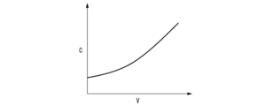
- 5A and 5B are diagrams illustrating capacitance changes of a variable capacitor according to the first embodiment.
- FIG. 11 is a diagram showing a change in capacitance of a variable capacitor according to a second embodiment.
- FIG. 13 is a plan view of a variable capacitor according to a third embodiment.
- FIG. 11 is a cross-sectional view of a variable capacitor according to a third embodiment.
- the directions are defined.
- the x and y directions are approximately parallel to one surface of the substrate Sub (see, for example, FIG. 4) described later.
- the x direction is, for example, the long axis direction of the first ferromagnetic layer.
- the y direction is perpendicular to the x direction.
- the z direction is the direction from the substrate Sub to the variable capacitor.
- the +z direction may be expressed as "up” and the -z direction as "down”, but these expressions are for convenience and do not define the direction of gravity.
- "extending in the x direction” means, for example, that the dimension in the x direction is larger than the smallest dimension among the dimensions in the x direction, y direction, and z direction. The same applies to extending in other directions.
- "connecting" is not limited to direct connection, but includes connection via another object.
- Fig. 1 is a plan view of the variable capacitor 100 according to the first embodiment.
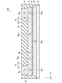
- Fig. 2 is a cross-sectional view of the variable capacitor 100 according to the first embodiment.
- Fig. 2 is a cross-sectional view taken along line AA in Fig. 1.
- the variable capacitor 100 has a first conductive layer 10, a second conductive layer 20, a capacitance layer 30, a first electrode 40, a second electrode 50, and a third electrode 60.
- the variable capacitor 100 changes in conductance in response to changes in the magnetization of the first conductive layer 10 and the second conductive layer 20 that sandwich the capacitance layer 30.
- the variable capacitor 100 is surrounded by, for example, an insulating layer 90.
- the insulating layer 90 is an insulating layer that provides insulation between the wirings of the multilayer wiring and between the elements.
- the insulating layer 90 is, for example, silicon oxide (SiO x ), silicon nitride (SiN x ), silicon carbide (SiC), chromium nitride, silicon carbonitride (SiCN), silicon oxynitride (SiON), aluminum oxide (Al 2 O 3 ), zirconium oxide (ZrO x ), or the like.
- the first conductive layer 10 is in contact with the capacitance layer 30.
- the length of the first conductive layer 10 in the x direction is longer than its length in the y direction.
- the first conductive layer 10 is a ferromagnetic layer that includes a ferromagnetic material.
- the first conductive layer 10 may be a ferromagnetic layer made of a ferromagnetic material.
- the ferromagnetic material may be, for example, a metal selected from the group consisting of Cr, Mn, Co, Fe, and Ni, an alloy containing one or more of these metals, or an alloy containing these metals and at least one of the elements B, C, and N.
- the ferromagnetic material may include, for example, any one selected from the group consisting of a CoPt alloy, a CoNi alloy, a TbFeCo alloy, a CoFe alloy, and alloys in which some of these alloys have been substituted.
- the ferromagnetic material is, for example, Co-Fe, Co-Fe-B, or Ni-Fe.
- the ferromagnetic material may be, for example, a Heusler alloy.
- the Heusler alloy is a half metal and has a high spin polarizability.
- the Heusler alloy is an intermetallic compound having a chemical composition of XYZ or X 2 YZ, where X is a transition metal element or a noble metal element of the Co, Fe, Ni, or Cu group on the periodic table, Y is a transition metal element or an element type of X of the Mn, V, Cr, or Ti group, and Z is a typical element of groups III to V.
- Examples of Heusler alloys include Co 2 FeSi, Co 2 FeGe, Co 2 FeGa, Co 2 MnSi, Co 2 Mn 1-a Fe a Al b Si 1-b , and Co 2 FeGe 1-c Ga c .
- the first conductive layer 10 has a first magnetic domain A1 and a second magnetic domain A2.
- a domain wall DW exists at the boundary between the first magnetic domain A1 and the second magnetic domain A2.
- the domain wall DW is configured so that it can move in a first direction within the plane of the first conductive layer 10, at least in the region of the first conductive layer 10 that overlaps with the capacitance layer 30 in the stacking direction.
- the domain wall DW is configured so that it can move in the x direction within the first conductive layer 10.
- the domain wall DW moves in the x direction by changing the potential difference between the first electrode 40 and the second electrode 50.
- the domain wall DW moves, for example, by applying a write current (e.g., a current pulse) in the x direction of the first conductive layer 10, or by applying an external magnetic field to the first conductive layer 10.
- a write current e.g., a current pulse
- an external magnetic field e.g., an external magnetic field
- the first magnetic domain A1 has a first region A11 and a second region A12.
- the magnetizations in the first magnetic domain A1 are oriented in the same direction.
- the magnetization M A11 of the first region A11 and the magnetization M A12 of the second region A12 are oriented in the same direction.
- the first region A11 is a region that overlaps with the first electrode 40 when viewed from the z direction, and is a region in which the magnetization M A11 is fixed.
- the magnetization being fixed means that the magnetization does not reverse during normal operation of the variable capacitor 100 (when no external force exceeding the expected value is applied).
- the first region A11 is called the first magnetization fixed region.
- the second region A12 is the region other than the first region A11 within the first magnetic domain A1.
- the volume of the second region A12 changes as the domain wall DW moves.
- the second magnetic domain A2 has a third region A21 and a fourth region A22.
- the magnetizations in the second magnetic domain A2 are oriented in the same direction.
- the magnetizations in the second magnetic domain A2 are oriented in a different direction from the magnetizations in the first magnetic domain A1.
- the magnetizations M A21 of the third region A21 and the magnetizations M A22 of the fourth region A22 are oriented in the same direction.
- the third region A21 is a region that overlaps with the second electrode 50 when viewed from the z direction, and is a region in which the magnetization M A21 is fixed.
- the third region A21 is referred to as a second magnetization fixed region.
- the fourth region A22 is the region other than the third region A21 in the second magnetic domain A2.
- the volume of the fourth region A22 changes when the domain wall DW moves.
- the second region A12 and the fourth region A22 are collectively referred to as the domain wall motion region.
- the domain wall motion region is sandwiched between the first magnetization fixed region and the second magnetization fixed region.
- the second conductive layer 20 is in contact with the capacitance layer 30.
- the first conductive layer 10 and the second conductive layer 20 sandwich the capacitance layer 30.
- the second conductive layer 20 is a ferromagnetic layer containing a ferromagnetic material.
- the second conductive layer 20 may be a ferromagnetic layer made of a ferromagnetic material.
- the second conductive layer 20 may be made of the same material as the material constituting the first conductive layer 10.
- the material constituting the second conductive layer 20 and the material constituting the first conductive layer 10 may be the same or different.
- the magnetization M20 of the second conductive layer 20 is more difficult to reverse than the magnetization of the first conductive layer 10.
- the second conductive layer 20 is, for example, closer to a substrate Sub (described later) than the first conductive layer 10. Such an element structure is called a bottom pin structure.
- the second conductive layer 20 contains the first conductive layer 10 when viewed from the z direction, for example. If the area of the second conductive layer 20 is larger than the area of the first conductive layer 10, the flatness of the first conductive layer 10 is improved, and the movement of the domain wall DW becomes smoother.
- the capacitance layer 30 is sandwiched between the first conductive layer 10 and the second conductive layer 20.
- the capacitance layer 30 is a dielectric layer.
- the capacitance layer 30 is insulating, and electric charges are stored in the first conductive layer 10 and the second conductive layer 20 that sandwich the capacitance layer 30.
- the capacitance layer 30 includes, for example, any one selected from the group consisting of magnesium oxide (MgO), aluminum oxide (Al2O3), titanium oxide (TiO2 ) , barium titanate ( BaTiO3 ), magnesium aluminate ( MgAl2O4 ), silicon oxide ( SiO2 ), magnesium titanate ( MgTiO3 ), and hafnium oxide ( HfO2 ).
- the composition ratio of each element in these oxides is not limited to the stoichiometric composition. When the capacitance layer 30 includes these materials, the change range of the capacitance of the variable capacitor 100 becomes large.
- the capacitance layer 30 may contain, for example, aluminum nitride (AlN) or aluminum nitride doped with any element selected from the group consisting of calcium, strontium, titanium, and potassium.
- AlN aluminum nitride
- AlN aluminum nitride
- any element selected from the group consisting of calcium, strontium, titanium, and potassium it has the effect of increasing the capacitance.
- the electrical conductivity of the capacitance layer 30 is improved, and heat generation due to current flow can be suppressed. As a result, it is possible to suppress large changes in the temperature of the variable capacitor 100 during use. This is an important characteristic when used in extreme environments.
- the capacitance layer 30 may include any one selected from the group consisting of lead titanate ( PbTiO3 ), strontium titanate ( SrTiO3 ), lead zirconate ( PbZrO3 ), lead hafnate ( PbHfO3 ), and relaxor ferroelectrics.
- PbTiO3 lead titanate
- SrTiO3 strontium titanate
- PbZrO3 lead zirconate
- PbHfO3 lead hafnate
- relaxor ferroelectrics relaxor ferroelectrics.
- the relaxor dielectric is a complex perovskite oxide represented by A(B'B") O3 .
- A(B'2 +1 / 3B" 5 +2/3 ) O3 and A(B'3 +1 / 2B" 5+ 1/2 ) O3 are examples of relaxor dielectrics.
- Pb(Mg1 / 3Nb2/3 ) O3 , Pb(Zn1 / 3Nb2/3 ) O3 , Pb( In1 /2Nb1/ 2 ) O3 , Pb(Sc1/ 2Nb1 / 2 ) O3 and Pb(Mg1 / 2W1/2 ) O3 are specific examples of relaxor dielectrics.
- the thickness of the capacitance layer 30 is, for example, 35 ⁇ or more, and preferably 100 ⁇ or more. If the capacitance layer 30 is sufficiently thick, the insulation of the capacitance layer 30 is ensured, and the variable capacitor 100 functions stably.
- the electrical resistance of the capacitance layer 30 is, for example, 1 M ⁇ or more, and preferably 10 M ⁇ or more. When the insulation of the capacitance layer 30 is ensured, the variable capacitor 100 functions stably.
- the lattice matching between the capacitance layer 30 and the first conductive layer 10 is, for example, less than 10%, and preferably 5% or less.
- the lattice matching between the capacitance layer 30 and the second conductive layer 20 is, for example, less than 10%, and preferably 5% or less.
- Lattice matching means that atoms are arranged continuously in the stacking direction at the interface between adjacent layers.
- the lattice matching degree is a value obtained by dividing the difference between the lattice constant of the capacitance layer 30 and the lattice constant of the adjacent layer (first conductive layer 10 or second conductive layer 20) by the lattice constant of the adjacent layer (first conductive layer 10 or second conductive layer 20).
- At least one of the first conductive layer 10, the capacitance layer 30, and the second conductive layer 20 is epitaxially grown from the substrate Sub. If these layers are epitaxially grown, the range of change in capacitance of the variable capacitor 100 will be large.
- the degree of lattice matching between the capacitance layer 30 and the first conductive layer 10 may be, for example, 10% or more.
- the degree of lattice matching between the capacitance layer 30 and the second conductive layer 20 may be, for example, 10% or more.
- the capacitance layer 30 and the adjacent layer are not lattice-matched, and some of the atoms at the interface between these layers are not continuously arranged. In other words, the capacitance layer 30 is not epitaxially grown from the substrate Sub.
- the capacitance layer 30 only needs to maintain the insulation between the first conductive layer 10 and the second conductive layer 20, and the interface between them does not need to be lattice-matched. If the capacitance layer 30 is not lattice-matched with the adjacent layer, the contact resistance at the interface increases, and the capacitance of the variable capacitor 100 increases. In addition, either the capacitance layer 30 and the first conductive layer 10 or the second conductive layer 20 may be amorphous, and there may be no lattice matching at the interface between the capacitance layer 30 and the first conductive layer 10 or the second conductive layer 20. If there is no lattice matching between the capacitance layer 30 and the adjacent layer, each layer is less susceptible to the influence of the adjacent layer, and the variation in device characteristics between multiple devices is reduced.
- the first electrode 40 contacts a part of the first conductive layer 10 directly or indirectly. Indirect contact means that another layer is sandwiched between the first electrode 40 and the first conductive layer 10.
- the first electrode 40 contacts, for example, a first end of the first conductive layer 10.
- the first electrode 40 contacts, for example, a first magnetic domain A1 of the first conductive layer 10.
- the first electrode 40 is, for example, a ferromagnetic layer.
- the same material as the first conductive layer 10 and the second conductive layer 20 can be used for the first electrode 40.
- the magnetization M40 of the first electrode 40 is oriented in the same direction as the magnetization M A11 of the first region A11 and fixes the magnetization M A11 of the first region A11.
- the first electrode 40 does not have to be a ferromagnetic layer.
- the current density of the current flowing through the first conductive layer 10 drops sharply at the position from the second region A12 to the first region A11. If the current density of the current flowing through the first conductive layer 10 drops sharply, the domain wall DW will not be able to penetrate into the first region A11, so the first electrode 40 does not have to be a ferromagnetic material.
- the second electrode 50 is in direct or indirect contact with a portion of the first conductive layer 10.
- the second electrode 50 is in contact with, for example, the second end of the first conductive layer 10.
- the second electrode 50 and the first electrode 40 are spaced apart in the x-direction.
- the second electrode 50 is in contact with, for example, the second magnetic domain A2 of the first conductive layer 10.
- the second electrode 50 is, for example, a ferromagnetic layer.
- the same material as the first electrode 40 can be applied to the second electrode 50.
- the magnetization M50 of the second electrode 50 fixes the magnetization M21 of the third region A21.
- the second electrode 50 is not limited to a ferromagnetic layer.
- the third electrode 60 is in contact with the second conductive layer 20.
- the third electrode 60 is a conductor.
- variable capacitor 100 may have layers other than those mentioned above.
- the variable capacitor 100 may have a nonmagnetic layer in contact with the surface of the second conductive layer 20 opposite the surface in contact with the capacitance layer 30, and a ferromagnetic layer sandwiching the nonmagnetic layer with the second conductive layer 20.
- the second conductive layer 20, the nonmagnetic layer, and the ferromagnetic layer form a synthetic antiferromagnetic structure (SAF structure).
- SAF structure increases the coercive force of the second conductive layer 20.
- the magnetization direction of each layer of the variable capacitor 100 can be confirmed, for example, by measuring the magnetization curve.
- the magnetization curve can be measured, for example, using MOKE (Magneto Optical Kerr Effect). Measurement using MOKE is a measurement method in which linearly polarized light is incident on the object being measured, and the magneto-optical effect (magnetic Kerr effect) is used to cause the polarization direction to rotate, etc.
- MOKE Magnetic Magnetic Kerr Effect
- the variable capacitor 100 is formed by a process of stacking each layer and a process of processing a part of each layer into a predetermined shape.
- the layers can be stacked using a sputtering method, a chemical vapor deposition (CVD) method, an electron beam evaporation method (EB evaporation method), an atomic laser deposition method, etc.
- the layers can be processed using photolithography and etching (e.g., Ar etching), etc.
- variable capacitor 100 performs a capacitance adjustment process and a charge accumulation process.
- the capacitance adjustment process of the variable capacitor 100 is explained below.
- a potential difference is applied between the first electrode 40 and the second electrode 50, and a write current (write pulse) is applied to the first conductive layer 10.
- the capacitance of the variable capacitor 100 changes to an analog value by applying an electrical signal in one direction within the plane of the first conductive layer 10.
- the write current moves the domain wall DW in the first conductive layer 10.
- the position of the domain wall DW changes depending on the magnitude of the write current (write pulse).
- the capacitance of the variable capacitor 100 increases as the region in which the second conductive layer 20, the magnetization M20 , and the magnetization of the first conductive layer 10 are antiparallel expands, and decreases as the region in which the second conductive layer 20, the magnetization M20 , and the magnetization of the first conductive layer 10 are parallel expands.
- the capacitance of the variable capacitor 100 increases as the first magnetic domain A1 expands, and the capacitance of the variable capacitor 100 decreases as the second magnetic domain A2 expands.
- variable capacitor 100 In the charge accumulation process, a potential difference is applied between the second electrode 50 and the third electrode 60. When a potential difference is applied between the second electrode 50 and the third electrode 60, charge is accumulated in each of the first conductive layer 10 and the second conductive layer 20.
- the capacitance of the variable capacitor 100 is determined by the capacitance adjustment process, and the variable capacitor 100 accumulates charge according to this capacitance and functions as a normal capacitor.
- the capacitance of the variable capacitor 100 is determined by the magnetization state of the two ferromagnetic layers that sandwich the capacitance layer 30, so in principle the capacitance changes even in extreme environments.
- the variable capacitor 100 has a minimum capacitance of 1 pF or more in extreme temperature ranges of 10 K or less or 1000 K or more.
- variable capacitor 100 is made of a laminate of thin films and is small in size. Furthermore, the variable capacitor 100 of this embodiment does not require a mechanical operating mechanism to change the capacitance, making it possible to miniaturize the device. Furthermore, the variable capacitor 100 of this embodiment changes the capacitance in an analog manner in response to an electrical signal, rather than a mechanical operation.
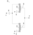
- FIG. 3 is a circuit diagram of a portion of the integrated circuit 200 according to the first embodiment.
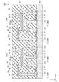
- FIG. 4 is a cross-sectional view of a portion of the integrated circuit 200 according to the first embodiment.
- the integrated circuit 200 includes a first variable capacitor 100A and a second variable capacitor 100B.
- the first variable capacitor 100A and the second variable capacitor 100B are each the variable capacitor 100 described above.
- the first variable capacitor 100A and the second variable capacitor 100B each perform a capacitance adjustment process by turning on the first switching element SW1 and the third switching element SW3 to adjust the potential between the write wiring WL and the common wiring CL.
- Each of the first variable capacitor 100A and the second variable capacitor 100B performs charge accumulation processing by turning on the second switching element SW2 and the third switching element SW3 to adjust the potential between the readout line RL and the common line CL.
- the first variable capacitor 100A and the second variable capacitor 100B are connected in parallel between the readout line RL and the common line CL. By connecting the first variable capacitor 100A and the second variable capacitor 100B in parallel, the maximum value of the combined capacitance of the two variable capacitors can be increased.
- the first switching element SW1, the second switching element SW2, and the third switching element SW3 are elements that control the flow of current.
- the first switching element SW1, the second switching element SW2, and the third switching element SW3 are, for example, elements that utilize a phase change in a crystal layer such as a transistor or an Ovonic Threshold Switch (OTS), elements that utilize a change in band structure such as a Metal-Insulator Transition (MIT) switch, elements that utilize a breakdown voltage such as a Zener diode or an avalanche diode, and elements whose conductivity changes with a change in atomic position.
- OTS Ovonic Threshold Switch
- MIT Metal-Insulator Transition
- the switching element and the variable capacitor are electrically connected by via wiring Vw and in-plane wiring IPw.
- the capacitance of the first variable capacitor 100A and the second variable capacitor 100B may be the same or different.
- the capacitance of the first variable capacitor 100A may be greater than the capacitance of the second variable capacitor 100B.
- the combined capacitance of the two variable capacitors can be roughly adjusted by the first variable capacitor 100A and finely adjusted by the second variable capacitor 100B.
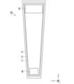
- Second Embodiment Fig. 5 is a plan view of the variable capacitor 101 according to the second embodiment.
- the cross-sectional view of the variable capacitor 101 according to the second embodiment is similar to that of Fig. 2.
- the same components as those in the variable capacitor 100 are denoted by the same reference numerals, and the description thereof will be omitted.
- the variable capacitor 101 has a first conductive layer 11, a second conductive layer 21, and a capacitance layer 31.
- the first conductive layer 11 corresponds to the first conductive layer 10 except for its shape in a plan view.
- the second conductive layer 21 corresponds to the second conductive layer 20 except for its shape in a plan view.
- the capacitance layer 31 corresponds to the capacitance layer 30 except for its shape in a plan view.
- the first conductive layer 11, the second conductive layer 21, and the capacitance layer 31 each have a non-constant width in the y direction when viewed from the z direction.
- the widths of these layers gradually increase from the first end to the second end in the x direction.
- the first conductive layer 11 gradually increases from the first end to the second end of the first conductive layer 11.
- the widths of these layers may also gradually decrease from the first end to the second end in the x direction.
- FIG. 6 is a diagram showing the capacitance change of the variable capacitor 100 according to the first embodiment.
- FIG. 7 is a diagram showing the capacitance change of the variable capacitor 101 according to the second embodiment.
- the horizontal axis is the strength of the energy applied in the capacitance adjustment process, such as the write voltage or the number of times the write pulse is applied.
- the vertical axis is the capacitance of the variable capacitor 100.
- variable capacitor 101 according to the second embodiment has the same effect as the variable capacitor 100 according to the first embodiment.
- the width of the first conductive layer 11 in the y direction is not constant, the state of change in capacitance of the variable capacitor 101 can be freely set.
- the variable capacitor 101 can be applied to the first variable capacitor 100A and the second variable capacitor 100B of the integrated circuit 200 described above.
- Fig. 8 is a plan view of the variable capacitor 102 according to the third embodiment.
- Fig. 9 is a cross-sectional view of the variable capacitor 102 according to the third embodiment, taken along line A-A in Fig. 8.
- the same components as those in the variable capacitor 100 are denoted by the same reference numerals, and description thereof will be omitted.
- the variable capacitor 102 differs from the variable capacitor 100 in the positional relationship between the first conductive layer 10 and the second conductive layer 20.
- the variable capacitor 102 has the second conductive layer 20 located away from the substrate Sub, and is said to have a top pin structure.
- variable capacitor 102 according to the third embodiment has the same effect as the variable capacitor 100 according to the first embodiment.
- the variable capacitor 102 can also be applied to the first variable capacitor 100A and the second variable capacitor 100B of the integrated circuit 200 described above.
Landscapes
- Engineering & Computer Science (AREA)
- Power Engineering (AREA)
- Microelectronics & Electronic Packaging (AREA)
- Semiconductor Integrated Circuits (AREA)
- Hall/Mr Elements (AREA)
Abstract
Description
図1は、第1実施形態に係る可変コンデンサ100の平面図である。図2は、第1実施形態に係る可変コンデンサ100の断面図である。図2は、図1のA-A線に沿って切断した断面である。
「格子整合度」=「(キャパシタンス層30の格子定数)-(第1導電層10の格子定数)」/「第1導電層10の格子定数」×100
図5は、第2実施形態に係る可変コンデンサ101の平面図である。第2実施形態に係る可変コンデンサ101の断面図は、図2と同様である。可変コンデンサ101において、可変コンデンサ100と同様の構成には同様の符号を付し、説明を省く。
図8は、第3実施形態に係る可変コンデンサ102の平面図である。図9は、第3実施形態に係る可変コンデンサ102の断面図であり、図8のA-A線に沿って切断した断面である。可変コンデンサ102において、可変コンデンサ100と同様の構成には同様の符号を付し、説明を省く。
Claims (15)
- 第1導電層と、第2導電層と、前記第1導電層と前記第2導電層とに挟まれるキャパシタンス層と、を有し、
前記第1導電層と前記第2導電層とはそれぞれ、強磁性体を含む強磁性層であり、
前記第1導電層は、第1磁区と、前記第1磁区と異なる方向に磁化が配向した第2磁区と、を有し、
前記第1磁区と前記第2磁区との境界である磁壁が、少なくとも前記第1導電層の前記キャパシタンス層と積層方向に重なる領域を、前記第1導電層の面内の第1方向に移動できるように構成されている、可変コンデンサ。 - 第1電極と第2電極とをさらに有し、
前記第1電極は、前記第1導電層の前記第1磁区と接し、
前記第2電極は、前記第1導電層の前記第2磁区と接する、請求項1に記載の可変コンデンサ。 - 前記第1電極は、強磁性層であり、
前記第1電極の磁化は、前記第1磁区の磁化と同じ方向に配向している、請求項2に記載の可変コンデンサ。 - 前記第2電極は、強磁性層であり、
前記第2電極の磁化は、前記第2磁区の磁化と同じ方向に配向している、請求項2に記載の可変コンデンサ。 - 前記キャパシタンス層は、酸化マグネシウム、酸化アルミニウム、酸化チタン、チタン酸バリウム、アルミン酸マグネシウム、酸化シリコン、チタン酸マグネシウム、酸化ハフニウムからなる群から選択されるいずれかを含む、請求項1に記載の可変コンデンサ。
- 前記キャパシタンス層は、窒化アルミニウム又は窒化アルミニウムにカルシウム、ストロンチウム、チタン、カリウムからなる群から選択されるいずれかが添加されたものを含む、請求項1に記載の可変コンデンサ。
- 前記キャパシタンス層は、チタン酸鉛、チタン酸ストロンチウム、ジルコン酸鉛、ハフニウム酸鉛、リラクサー強誘電体からなる群から選択されるいずれかを含む、請求項1に記載の可変コンデンサ。
- 前記第1導電層又は前記第2導電層は、ホイスラー合金、CoPt合金、CoNi合金、TbFeCo合金、CoFe合金、これらの合金のうちの一部が置換されたものからなる群から選択されるいずれかを含む、請求項1に記載の可変コンデンサ。
- 基板をさらに有し、
前記第1導電層、前記キャパシタンス層、前記第2導電層のうちの少なくとも一つは、前記基板からエピタキシャル成長している、請求項1に記載の可変コンデンサ。 - 前記キャパシタンス層の格子定数と前記第1導電層の格子定数との差を前記第1導電層の格子定数で割って求められる格子整合度が、10%以上である、請求項1に記載の可変コンデンサ。
- 前記第1導電層は、前記積層方向から見て、前記第1方向と直交する第2方向の幅が一定ではなく、
前記幅は、前記第1導電層の第1端から第2端に向かって、徐々に広がる又は徐々に狭まる、請求項1に記載の可変コンデンサ。 - 10K以下又は1000K以上の温度領域において、キャパシタンスの最小値が1pF以上である、請求項1に記載の可変コンデンサ。
- 第1導電層と、第2導電層と、前記第1導電層と前記第2導電層とに挟まれるキャパシタンス層と、を有し、
前記第1導電層と前記第2導電層とはそれぞれ、強磁性体を含む強磁性層であり、
前記第1導電層の面内の一方向に電気信号を印加することによって、キャパシタンス量がアナログに変化する、可変コンデンサ。 - 第1可変コンデンサと、第2可変コンデンサと、を備え、
前記第1可変コンデンサと前記第2可変コンデンサとはそれぞれ、請求項1に記載の可変コンデンサであり、
前記第1可変コンデンサと前記第2可変コンデンサとは並列接続されている、集積回路。 - 前記第1可変コンデンサと前記第2可変コンデンサとは、キャパシタンスが異なる、請求項13に記載の集積回路。
Priority Applications (3)
| Application Number | Priority Date | Filing Date | Title |
|---|---|---|---|
| US18/025,812 US12477755B2 (en) | 2022-10-11 | 2022-10-11 | Variable capacitor and integrated circuit |
| PCT/JP2022/037856 WO2024079783A1 (ja) | 2022-10-11 | 2022-10-11 | 可変コンデンサ及び集積回路 |
| CN202280006598.8A CN118176554A (zh) | 2022-10-11 | 2022-10-11 | 可变电容器及集成电路 |
Applications Claiming Priority (1)
| Application Number | Priority Date | Filing Date | Title |
|---|---|---|---|
| PCT/JP2022/037856 WO2024079783A1 (ja) | 2022-10-11 | 2022-10-11 | 可変コンデンサ及び集積回路 |
Publications (1)
| Publication Number | Publication Date |
|---|---|
| WO2024079783A1 true WO2024079783A1 (ja) | 2024-04-18 |
Family
ID=90668951
Family Applications (1)
| Application Number | Title | Priority Date | Filing Date |
|---|---|---|---|
| PCT/JP2022/037856 Ceased WO2024079783A1 (ja) | 2022-10-11 | 2022-10-11 | 可変コンデンサ及び集積回路 |
Country Status (3)
| Country | Link |
|---|---|
| US (1) | US12477755B2 (ja) |
| CN (1) | CN118176554A (ja) |
| WO (1) | WO2024079783A1 (ja) |
Citations (6)
| Publication number | Priority date | Publication date | Assignee | Title |
|---|---|---|---|---|
| WO2008001914A1 (fr) * | 2006-06-29 | 2008-01-03 | Kyocera Corporation | Ensemble de condensateurs à capacitance variable, dispositif d'ensemble de condensateurs à capacitance variable et module |
| US20110051313A1 (en) * | 2009-09-02 | 2011-03-03 | Hwang Wein-Kuen | Magnetically enhanced capacitance for high performance thin film capacitors |
| US20140313637A1 (en) * | 2013-04-23 | 2014-10-23 | Alexander Mikhailovich Shukh | Magnetic Capacitor |
| JP2015073047A (ja) * | 2013-10-04 | 2015-04-16 | 太陽誘電株式会社 | 可変容量デバイス |
| US20150179345A1 (en) * | 2012-05-24 | 2015-06-25 | The Board Of Trustees Of The University Of Alabama For And On Behalf Of The University Of Alabama | Magnetic Supercapacitors |
| WO2021199233A1 (ja) * | 2020-03-31 | 2021-10-07 | Tdk株式会社 | 磁気抵抗効果素子 |
Family Cites Families (19)
| Publication number | Priority date | Publication date | Assignee | Title |
|---|---|---|---|---|
| JPH088142A (ja) | 1994-04-18 | 1996-01-12 | Meidensha Corp | 真空コンデンサ |
| US6381171B1 (en) * | 1999-05-19 | 2002-04-30 | Kabushiki Kaisha Toshiba | Magnetic element, magnetic read head, magnetic storage device, magnetic memory device |
| WO2005046114A2 (en) | 2003-11-05 | 2005-05-19 | Northwestern University | Coherent-states based quantum data-encryption through optically-amplified wdm communication networks |
| JP2006133726A (ja) | 2004-10-06 | 2006-05-25 | Kanagawa Acad Of Sci & Technol | 酸化物材料、光磁気デバイス、ファラデー回転係数制御方法、磁気抵抗効果素子、磁気メモリ素子、残留磁化制御方法及び保持力制御方法 |
| JP5434373B2 (ja) | 2009-08-26 | 2014-03-05 | 沖電気工業株式会社 | 量子もつれ光子対発生装置 |
| JP5434440B2 (ja) | 2009-09-30 | 2014-03-05 | 沖電気工業株式会社 | 量子もつれ光子対発生装置 |
| JP2013025253A (ja) | 2011-07-25 | 2013-02-04 | Oki Electric Ind Co Ltd | 偏波量子もつれ光子対発生装置 |
| JP5867232B2 (ja) | 2012-03-29 | 2016-02-24 | 沖電気工業株式会社 | 量子もつれ光子対発生装置 |
| JP2014067060A (ja) | 2013-12-11 | 2014-04-17 | Oki Electric Ind Co Ltd | 量子もつれ光子対発生装置 |
| JP2014067061A (ja) | 2013-12-11 | 2014-04-17 | Oki Electric Ind Co Ltd | 量子もつれ光子対発生装置 |
| US9843312B2 (en) | 2015-09-30 | 2017-12-12 | International Business Machines Corporation | Multimode Josephson parametric converter: coupling Josephson ring modulator to metamaterial |
| US9818064B1 (en) | 2016-10-11 | 2017-11-14 | International Business Machines Corporation | High fidelity threshold detection of single microwave photons using a quantum non-demolition photon detector |
| US9870536B1 (en) | 2017-04-04 | 2018-01-16 | International Business Machines Corporation | Integrated drive and readout circuit for superconducting qubits |
| US10398031B2 (en) | 2017-09-29 | 2019-08-27 | International Business Machines Corporation | Integrating Josephson amplifiers or Josephson mixers into printed circuit boards |
| US10629978B2 (en) | 2017-10-30 | 2020-04-21 | International Business Machines Corporation | Multi-path interferometric Josephson isolator based on nondegenerate three-wave mixing Josephson devices |
| CA3109380C (en) | 2017-12-15 | 2022-10-18 | Google Llc | Compact multi-pole quantum bit measurement filter |
| US11620559B2 (en) | 2019-02-06 | 2023-04-04 | International Business Machines Corporation | Reduction of spontaneous emission and thermal photon noise in quantum computing machines using a galvanically grounded filter |
| US10892398B2 (en) | 2019-03-28 | 2021-01-12 | Johannes Pollanen | Qubit hardware for electrons on helium |
| US11940392B2 (en) | 2019-04-18 | 2024-03-26 | International Business Machines Corporation | Measurement scheme for superconducting qubits using low-frequency microwave signals within a dilution refrigerator |
-
2022
- 2022-10-11 US US18/025,812 patent/US12477755B2/en active Active
- 2022-10-11 WO PCT/JP2022/037856 patent/WO2024079783A1/ja not_active Ceased
- 2022-10-11 CN CN202280006598.8A patent/CN118176554A/zh active Pending
Patent Citations (6)
| Publication number | Priority date | Publication date | Assignee | Title |
|---|---|---|---|---|
| WO2008001914A1 (fr) * | 2006-06-29 | 2008-01-03 | Kyocera Corporation | Ensemble de condensateurs à capacitance variable, dispositif d'ensemble de condensateurs à capacitance variable et module |
| US20110051313A1 (en) * | 2009-09-02 | 2011-03-03 | Hwang Wein-Kuen | Magnetically enhanced capacitance for high performance thin film capacitors |
| US20150179345A1 (en) * | 2012-05-24 | 2015-06-25 | The Board Of Trustees Of The University Of Alabama For And On Behalf Of The University Of Alabama | Magnetic Supercapacitors |
| US20140313637A1 (en) * | 2013-04-23 | 2014-10-23 | Alexander Mikhailovich Shukh | Magnetic Capacitor |
| JP2015073047A (ja) * | 2013-10-04 | 2015-04-16 | 太陽誘電株式会社 | 可変容量デバイス |
| WO2021199233A1 (ja) * | 2020-03-31 | 2021-10-07 | Tdk株式会社 | 磁気抵抗効果素子 |
Also Published As
| Publication number | Publication date |
|---|---|
| US20240290822A1 (en) | 2024-08-29 |
| US12477755B2 (en) | 2025-11-18 |
| CN118176554A (zh) | 2024-06-11 |
Similar Documents
| Publication | Publication Date | Title |
|---|---|---|
| Kirbach et al. | Doping concentration dependent piezoelectric behavior of Si: HfO2 thin-films | |
| US12131252B2 (en) | Neuromorphic device | |
| CN112599660B (zh) | 磁畴壁移动元件和磁记录阵列 | |
| US12058872B2 (en) | Integrated device and neuromorphic device | |
| Guerrero et al. | Growth and characterization of epitaxial ferroelectric PbZrxTi1− xO3 thin film capacitors with SrRuO3 electrodes for non-volatile memory applications | |
| CN114373780A (zh) | 磁畴壁移动元件及磁阵列 | |
| CN113793896B (zh) | 磁畴壁移动元件及磁存储阵列 | |
| JP7211564B1 (ja) | 磁壁移動素子、磁気アレイ及び磁壁移動素子の製造方法 | |
| JP2022188716A (ja) | 磁壁移動素子及び磁気アレイ | |
| Nguyen | Effect of substrate and electrode on the crystalline structure and energy storage performance of antiferroelectric PbZrO3 films | |
| US12477755B2 (en) | Variable capacitor and integrated circuit | |
| JP7666919B2 (ja) | 磁壁移動素子及び磁気アレイ | |
| US20250061322A1 (en) | Neuromorphic device | |
| US11139340B2 (en) | Spin element and reservoir element | |
| Pradhan et al. | Exploring phase transitions and magnetoelectric coupling of epitaxial asymmetric multilayer heterostructures | |
| JP7586745B2 (ja) | 磁壁移動素子及び磁気記録アレイ | |
| US11991931B2 (en) | Magnetic recording layer, magnetic domain wall moving element and magnetic recording array | |
| JP7470599B2 (ja) | 配線層、磁壁移動素子および磁気アレイ | |
| US20240420785A1 (en) | Magnetic domain wall motion element, magnetic recording array, and magnetic memory | |
| WO2023007609A1 (ja) | 磁壁移動素子および磁気アレイ | |
| WO2024004126A1 (ja) | 磁壁移動素子及び磁気アレイ | |
| JP7512116B2 (ja) | 磁気メモリ | |
| TWI870910B (zh) | 磁化旋轉元件、磁性阻抗效果元件及磁性記憶體 | |
| JP2025116325A (ja) | 磁気抵抗効果装置及び磁気メモリ | |
| US20240268237A1 (en) | Magnetic domain wall motion element and magnetic array |
Legal Events
| Date | Code | Title | Description |
|---|---|---|---|
| WWE | Wipo information: entry into national phase |
Ref document number: 18025812 Country of ref document: US |
|
| WWE | Wipo information: entry into national phase |
Ref document number: 202280006598.8 Country of ref document: CN |
|
| 121 | Ep: the epo has been informed by wipo that ep was designated in this application |
Ref document number: 22962004 Country of ref document: EP Kind code of ref document: A1 |
|
| NENP | Non-entry into the national phase |
Ref country code: DE |
|
| 122 | Ep: pct application non-entry in european phase |
Ref document number: 22962004 Country of ref document: EP Kind code of ref document: A1 |
|
| NENP | Non-entry into the national phase |
Ref country code: JP |
|
| WWG | Wipo information: grant in national office |
Ref document number: 18025812 Country of ref document: US |