WO2024070958A1 - 信号伝達装置 - Google Patents
信号伝達装置 Download PDFInfo
- Publication number
- WO2024070958A1 WO2024070958A1 PCT/JP2023/034535 JP2023034535W WO2024070958A1 WO 2024070958 A1 WO2024070958 A1 WO 2024070958A1 JP 2023034535 W JP2023034535 W JP 2023034535W WO 2024070958 A1 WO2024070958 A1 WO 2024070958A1
- Authority
- WO
- WIPO (PCT)
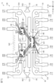
- Prior art keywords
- lead
- chip
- die pad
- wire
- connection portion
- Prior art date
- Legal status (The legal status is an assumption and is not a legal conclusion. Google has not performed a legal analysis and makes no representation as to the accuracy of the status listed.)
- Ceased
Links
Images



























Classifications
-
- H—ELECTRICITY
- H10—SEMICONDUCTOR DEVICES; ELECTRIC SOLID-STATE DEVICES NOT OTHERWISE PROVIDED FOR
- H10D—INORGANIC ELECTRIC SEMICONDUCTOR DEVICES
- H10D84/00—Integrated devices formed in or on semiconductor substrates that comprise only semiconducting layers, e.g. on Si wafers or on GaAs-on-Si wafers
-
- H—ELECTRICITY
- H10—SEMICONDUCTOR DEVICES; ELECTRIC SOLID-STATE DEVICES NOT OTHERWISE PROVIDED FOR
- H10D—INORGANIC ELECTRIC SEMICONDUCTOR DEVICES
- H10D84/00—Integrated devices formed in or on semiconductor substrates that comprise only semiconducting layers, e.g. on Si wafers or on GaAs-on-Si wafers
- H10D84/01—Manufacture or treatment
- H10D84/02—Manufacture or treatment characterised by using material-based technologies
- H10D84/03—Manufacture or treatment characterised by using material-based technologies using Group IV technology, e.g. silicon technology or silicon-carbide [SiC] technology
- H10D84/038—Manufacture or treatment characterised by using material-based technologies using Group IV technology, e.g. silicon technology or silicon-carbide [SiC] technology using silicon technology, e.g. SiGe
-
- H—ELECTRICITY
- H10—SEMICONDUCTOR DEVICES; ELECTRIC SOLID-STATE DEVICES NOT OTHERWISE PROVIDED FOR
- H10W—GENERIC PACKAGES, INTERCONNECTIONS, CONNECTORS OR OTHER CONSTRUCTIONAL DETAILS OF DEVICES COVERED BY CLASS H10
- H10W72/00—Interconnections or connectors in packages
-
- H—ELECTRICITY
- H10—SEMICONDUCTOR DEVICES; ELECTRIC SOLID-STATE DEVICES NOT OTHERWISE PROVIDED FOR
- H10W—GENERIC PACKAGES, INTERCONNECTIONS, CONNECTORS OR OTHER CONSTRUCTIONAL DETAILS OF DEVICES COVERED BY CLASS H10
- H10W72/00—Interconnections or connectors in packages
- H10W72/071—Connecting or disconnecting
-
- H—ELECTRICITY
- H10—SEMICONDUCTOR DEVICES; ELECTRIC SOLID-STATE DEVICES NOT OTHERWISE PROVIDED FOR
- H10W—GENERIC PACKAGES, INTERCONNECTIONS, CONNECTORS OR OTHER CONSTRUCTIONAL DETAILS OF DEVICES COVERED BY CLASS H10
- H10W74/00—Encapsulations, e.g. protective coatings
- H10W74/01—Manufacture or treatment
-
- H—ELECTRICITY
- H10—SEMICONDUCTOR DEVICES; ELECTRIC SOLID-STATE DEVICES NOT OTHERWISE PROVIDED FOR
- H10W—GENERIC PACKAGES, INTERCONNECTIONS, CONNECTORS OR OTHER CONSTRUCTIONAL DETAILS OF DEVICES COVERED BY CLASS H10
- H10W90/00—Package configurations
Definitions
- This disclosure relates to a signal transmission device.
- a signal transmission device that includes a first die pad, a second die pad arranged at a distance from the first die pad, a first chip and a transformer chip mounted on the first die pad, a second chip mounted on the second die pad, and a sealing resin that seals the die pads and chips (see, for example, Patent Document 1).
- the first chip and the transformer chip are electrically connected by a wire
- the transformer chip and the second chip are electrically connected by another wire.
- a signal transmission device includes a first chip including an isolation transformer, a second chip receiving a signal from the first chip and/or transmitting a signal to the first chip, a third chip receiving a signal from the first chip and/or transmitting a signal to the first chip, a first die pad on which the first chip is mounted, a second die pad arranged at a distance from the first die pad in a first direction and on which the second chip is mounted, a third die pad arranged at a distance from the first die pad in the first direction and at a distance from the second die pad in a second direction perpendicular to the first direction in a planar view, and on which the third chip is mounted, and a plurality of first lead terminals arranged on the opposite side of the first die pad from the second die pad and the third die pad in the first direction and arranged in the second direction in a plan view; a plurality of second lead terminals arranged on the opposite side of the first die pad from the second die pad and the third die pad in the first direction and arranged in the second
- the signal transmission device described above allows the wire height of the inter-chip wires to be inspected with greater precision.
- FIG. 1 is a perspective view of a signal transmission device according to a first embodiment.
- FIG. 2 is a side view of the signal transmission device of FIG.
- FIG. 3 is a side view of the signal transmission device of FIG. 1, seen from a different direction than that of FIG.
- FIG. 4 is an enlarged view of the first lead terminal and its periphery in FIG.
- FIG. 5 is an enlarged view of an end surface of an outer lead of the first lead terminal of FIG.
- FIG. 6 is a side view of the signal transmission device mounted on a circuit board.
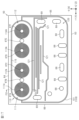
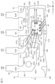
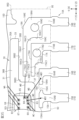
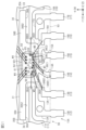
- FIG. 7 is a schematic plan view showing the internal configuration of the signal transmission device of FIG.
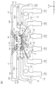
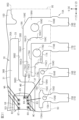
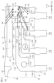
- FIG. 8 is an enlarged view of the first frame and its surroundings in FIG.
- FIG. 9 is an enlarged view of a part of the first frame and its surroundings in FIG.
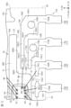
- FIG. 10 is an enlarged view of a remaining portion of the first frame in FIG. 8 and its surroundings.
- FIG. 11 is a schematic cross-sectional view of a wire connection portion of a first lead terminal.
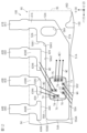
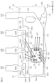
- FIG. 12 is an enlarged view of the second die pad and its periphery in FIG.
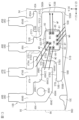
- FIG. 13 is an enlarged view of the third die pad and its periphery in FIG.
- FIG. 14 is a schematic cross-sectional view of a wire connection portion of the second lead terminal.
- FIG. 15 is an enlarged perspective view of the second bond portion of the third die pad wire and its surroundings.
- FIG. 16 is a circuit diagram of the signal transmission device of the first embodiment.
- FIG. 17 is a schematic plan view illustrating an example of the internal structure of the first chip in the signal transmission device according to the first embodiment.
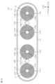
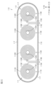
- FIG. 18 is an enlarged plan view of the transformer region of FIG.
- FIG. 19 is a schematic plan view showing an example of the internal structure of the first chip at a position different from that in FIG. 18 in the thickness direction of the first chip.
- FIG. 20 is an enlarged plan view of the transformer region of FIG.
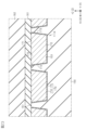
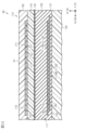
- FIG. 21 is a cross-sectional view showing the cross-sectional structure of the first transformer of the first chip and its periphery.
- FIG. 22 is an enlarged view of a part of the first chip in FIG.
- FIG. 23 is an enlarged view of the conductor of the first surface side coil in the first chip of FIG. 22.
- FIG. FIG. 24 is an enlarged view of the conductor wire of the first back side coil in the first chip in FIG. 22.
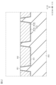
- FIG. 25 is a cross-sectional view showing a cross-sectional structure of a part of the circuit region of the first chip.
- FIG. 26 is an enlarged view of the first via and its periphery in FIG.
- FIG. 27 is an enlarged plan view of a part of the first frame and its periphery in the signal transmission device of the second embodiment.
- FIG. 28 is an enlarged plan view of the second die pad and its periphery in the signal transmission device of the second embodiment.
- FIG. 29 is an enlarged plan view of the third die pad and its periphery in the signal transmission device of the second embodiment.
- FIG. 30 is an enlarged plan view of a part of the first frame and its periphery in the signal transmission device of the third embodiment.
- FIG. 31 is an enlarged plan view of a remaining portion of the first frame and its periphery in the signal transmission device of the third embodiment.
- FIG. 32 is an enlarged plan view of the second die pad and its periphery in the signal transmission device of the third embodiment.
- FIG. 33 is an enlarged plan view of the third die pad and its periphery in the signal transmission device of the third embodiment.
- FIG. 34 is an enlarged plan view of a part of the first frame and its periphery in the signal transmission device of the fourth embodiment.
- FIG. 35 is an enlarged plan view of a remaining portion of the first frame and its periphery in the signal transmission device of the fourth embodiment.
- FIG. 36 is an enlarged plan view of the second die pad and its periphery in the signal transmission device of the fourth embodiment.
- FIG. 37 is an enlarged plan view of the third die pad and its periphery in the signal transmission device of the fourth embodiment.
- FIG. 38 is an enlarged plan view of a part of the first die pad, the third die pad, and the periphery thereof in the signal transmission device of the fifth embodiment.
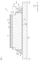
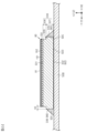
- FIG. 39 is a schematic cross-sectional view of a first chip and a first die pad in a signal transmission device according to the sixth embodiment.
- FIG. 40 is a schematic cross-sectional view of the first chip and the first die pad taken in a direction different from that of FIG.
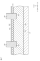
- FIG. 41 is a schematic cross-sectional view of the second chip and the second die pad.
- FIG. 42 is a schematic cross-sectional view of the second chip and the second die pad taken in a direction different from that of FIG. FIG.
- FIG. 43 is a schematic cross-sectional view of the third chip and the third die pad.
- FIG. 44 is a schematic cross-sectional view of the third chip and the third die pad taken in a direction different from that of FIG.
- FIG. 45 is a cross-sectional view illustrating an example of a manufacturing process for the signal transmission device of the sixth embodiment.
- FIG. 46 is a cross-sectional view showing a schematic example of a manufacturing process for the signal transmission device subsequent to FIG. 45.
- FIG. 47 is a cross-sectional view showing a schematic example of a manufacturing process for the signal transmission device following FIG. 46.
- FIG. 48 is a cross-sectional view showing a schematic example of a manufacturing process for the signal transmission device following FIG. 47.
- FIG. 46 is a cross-sectional view showing a schematic example of a manufacturing process for the signal transmission device following FIG. 46.
- FIG. 49 is a plan view illustrating a schematic internal structure of the signal transmission device according to the seventh embodiment.
- FIG. 50 is a plan view illustrating a schematic internal structure of the signal transmission device according to the eighth embodiment.
- FIG. 51 is an enlarged plan view of the first frame and its periphery in the signal transmission device of the ninth embodiment.
- FIG. 52 is an enlarged plan view of the first die pad and its periphery in the signal transmission device of the ninth embodiment.
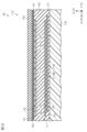
- FIG. 53 is a cross-sectional view showing a schematic example of a cross-sectional structure of a first transformer of a first chip and its periphery in a signal transmission device according to the tenth embodiment.
- FIG. 54 is an enlarged cross-sectional view of a part of the first transformer and its periphery in FIG.
- FIG. 55 is a cross-sectional view illustrating an example of a manufacturing process for the signal transmission device of the tenth embodiment.
- 56 is a cross-sectional view showing a schematic example of a manufacturing process for the signal transmission device following FIG. 55.
- FIG. 57 is a cross-sectional view showing a schematic example of a manufacturing process for the signal transmission device following FIG. 56.
- FIG. 58 is a cross-sectional view showing the cross-sectional structure of the first transformer of the first chip and part of its periphery in the signal transmission device of the eleventh embodiment.
- FIG. 60 is a cross-sectional view illustrating an example of a manufacturing process for the signal transmission device of the twelfth embodiment.
- 61 is a cross-sectional view showing a schematic example of a manufacturing process for the signal transmission device following FIG. 60.
- FIG. 62 is a cross-sectional view showing a schematic example of a manufacturing process for the signal transmission device following FIG. 61.
- FIG. 63 is a cross-sectional view showing a schematic example of a manufacturing process for the signal transmission device following FIG. 62.
- FIG. FIG. FIG. 60 is a cross-sectional view illustrating an example of a manufacturing process for the signal transmission device following FIG. 60.
- FIG. 64 is a cross-sectional view showing a schematic example of a manufacturing process for the signal transmission device following FIG. 63.
- 65 is a cross-sectional view showing a schematic example of a manufacturing process for the signal transmission device following FIG. 64.
- FIG. 66 is an enlarged cross-sectional view of a portion of the first surface side coil of the first transformer of the first chip and its surrounding area in the signal transmission device of the thirteenth embodiment.
- FIG. 67 is a cross-sectional view illustrating an example of a manufacturing process for the signal transmission device of the thirteenth embodiment.
- 68 is a cross-sectional view showing a schematic example of a manufacturing process for the signal transmission device following FIG. 67.
- FIG. 69 is a cross-sectional view showing a schematic example of a manufacturing process for the signal transmission device following FIG. 68.
- 70 is a cross-sectional view showing a schematic example of a manufacturing process for the signal transmission device subsequent to FIG. 69.
- FIG. 71 is a cross-sectional view showing a schematic example of a manufacturing process for the signal transmission device subsequent to FIG. 70.
- FIG. 72 is a schematic plan view showing an example of the internal structure of the first chip in a signal transmission device according to a modified example.
- FIG. 73 is a schematic plan view showing an example of the internal structure of the first chip at a position different from that in FIG. 72 in the thickness direction of the first chip.
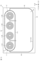
- FIG. 74 is a plan view showing a schematic internal structure of a signal transmission device according to a modified example.
- FIG. 75 is a plan view showing a schematic internal structure of a signal transmission device according to a modified example.
- FIG. 1 to 6 show the external structure of the signal transmission device 10.
- Figures 7 to 15 show the internal structure of the signal transmission device 10.
- Figure 16 shows the circuit configuration of the signal transmission device 10.
- Figures 17 to 26 show the internal structure of a first chip 60 (described later) of the signal transmission device 10.
- FIG. 1 shows a perspective view of the signal transmission device 10.
- Figs. 2 and 3 show a side view of the signal transmission device 10.
- Fig. 4 shows an enlarged view of a portion of a first lead terminal 18 of the signal transmission device 10, which will be described later.
- the package structure of the signal transmission device 10 is a small outline package (SOP).
- SOP small outline package
- the package structure of the signal transmission device 10 can be changed as desired, and may be a quad for non-lead package (QFN), dual flat package (DFP), dual inline package (DIP), quad flat package (QFP), single inline package (SIP), or small outline J-leaded package (SOJ), or various similar package structures.
- QFN quad for non-lead package
- DFP dual flat package
- DIP dual inline package
- QFP quad flat package
- SIP single inline package
- SOJ small outline J-leaded package
- the signal transmission device 10 includes a sealing resin 90, a plurality of first lead terminals 11-18 (eight in the first embodiment) protruding from the sealing resin 90, and a plurality of second lead terminals 41-48 (eight in the first embodiment) protruding from the sealing resin 90.
- the sealing resin 90 is formed in a rectangular plate shape.
- the thickness direction of the sealing resin 90 is the "Z direction", and two mutually perpendicular directions among the directions perpendicular to the Z direction are the "X direction” and the "Y direction”.
- the upper side of the Z direction is the "+Z direction", and the lower side is the "-Z direction”.
- the front side of the X direction is the "+X direction”
- the rear side is the "-X direction”.
- the right side of the Y direction is the "+Y direction”
- the left side is the "-Y direction”.
- planar view refers to viewing the signal transmission device 10 from the thickness direction of the sealing resin 90. Unless otherwise specified, planar view refers to viewing the signal transmission device 10 from the +Z direction.
- the shape of the sealing resin 90 in plan view is a rectangle with the X direction being the short side direction and the Y direction being the long side direction.
- the size of the sealing resin 90 in the Y direction is at least twice the size of the sealing resin 90 in the X direction.
- the size of the sealing resin 90 in the Y direction is no more than three times the size of the sealing resin 90 in the X direction. In one example, in plan view, the size of the sealing resin 90 in the Y direction is about 2.5 times the size of the sealing resin 90 in the X direction.
- the dimension of the sealing resin 90 in the X direction is about 4.0 mm
- the dimension of the sealing resin 90 in the Y direction is about 10.0 mm
- the dimension (thickness) of the sealing resin 90 in the Z direction is about 1.75 mm.
- the sealing resin 90 has a sealing surface 91, a sealing back surface 92 opposite the sealing surface 91, and first to fourth sealing side surfaces 93 to 96 connecting the sealing surface 91 and the sealing back surface 92.
- the sealing surface 91 is a surface facing the +Z direction
- the sealing back surface 92 is a surface facing the -Z direction.
- the first sealing side surface 93 and the second sealing side surface 94 form both end surfaces of the sealing resin 90 in the X direction
- the third sealing side surface 95 and the fourth sealing side surface 96 form both end surfaces of the sealing resin 90 in the Y direction.
- the first sealing side surface 93 is a surface facing the +X direction
- the second sealing side surface 94 is a surface facing the -X direction.
- the third sealing side surface 95 is a surface facing the +Y direction
- the fourth sealing side surface 96 is a surface facing the -Y direction.
- a recess 91A is formed in the sealing surface 91.
- the recess 91A is circular in a plan view.
- the recess 91A is recessed in a curved concave shape from the sealing surface 91.
- the recess 91A is formed in a portion of the sealing surface 91 that is closer to the first sealing side surface 93 and the fourth sealing side surface 96.
- the recess 91A serves as a marker for distinguishing the first lead terminals 11-18 from the second lead terminals 41-48.
- the first sealing side 93 includes a first front side 93A that is continuous with the sealing surface 91, a first back side 93B that is continuous with the sealing back surface 92, and a first central side 93C.
- the second sealing side 94 includes a second front side 94A that is continuous with the sealing surface 91, a second back side 94B that is continuous with the sealing back surface 92, and a second central side 94C.
- the first front side 93A and the second front side 94A are inclined in a direction away from each other as they move from the sealing surface 91 toward the sealing back surface 92.
- the connection portion between the first front side 93A and the sealing surface 91 is formed with an inclined surface 93AA.
- the angle formed by the inclined surface 93AA and the Z direction is larger than the angle formed by the first front side 93A and the Z direction.
- the angle formed by the inclined surface 93AA and the Z direction is, for example, 45°.
- the connection portion between the second front surface side surface 94A and the sealing surface 91 is formed in a curved shape.
- the first back surface side surface 93B and the second back surface side surface 94B are inclined in a direction away from each other as they move from the sealing back surface 92 to the sealing surface 91.
- the connection portion between the first back surface side surface 93B and the second back surface side surface 94B and the sealing back surface 92 is formed in a curved shape.
- the first central side surface 93C is formed between the first front surface side surface 93A and the first back surface side surface 93B in the Z direction.
- the first central side surface 93C is connected to both the first front surface side surface 93A and the first back surface side surface 93B.
- the first central side surface 93C is formed as a flat surface along, for example, the YZ plane.
- the second central side surface 94C is formed between the second front surface side surface 94A and the second back surface side surface 94B in the Z direction.
- the second central side surface 94C is connected to both the second front surface side surface 94A and the second back surface side surface 94B.
- the second central side surface 94C is formed as a flat surface along the YZ plane, for example.
- the third sealing side 95 includes a third front side 95A that is continuous with the sealing surface 91, a third back side 95B that is continuous with the sealing back surface 92, and a third central side 95C.
- the fourth sealing side 96 includes a fourth front side 96A that is continuous with the sealing surface 91, a fourth back side 96B that is continuous with the sealing back surface 92, and a fourth central side 96C.
- the third front side 95A and the fourth front side 96A are inclined in directions away from each other as they move from the sealing surface 91 to the sealing back surface 92.
- the connection portions between the third front side 95A and the fourth front side 96A and the sealing surface 91 are formed in a curved shape.
- the third back side 95B and the fourth back side 96B are inclined in directions away from each other as they move from the sealing back surface 92 to the sealing surface 91.
- the connection portions between the third back side 95B and the fourth back side 96B and the sealing back surface 92 are formed in a curved shape.
- the third central side surface 95C is connected to both the third front surface side surface 95A and the third back surface side surface 95B.
- the third central side surface 95C is formed, for example, as a flat surface along the XZ plane.
- the fourth central side surface 96C is formed between the fourth front surface side surface 96A and the fourth back surface side surface 96B in the Z direction.
- the fourth central side surface 96C is connected to both the fourth front surface side surface 96A and the fourth back surface side surface 96B.
- the fourth central side surface 96C is formed, for example, as a flat surface along the XZ plane.
- the sealing resin 90 is formed, for example, by transfer molding.
- the third sealing side surface 95 is provided with a trace (not shown) of the gate of the molding die. This trace is formed when the resin portion located at the gate of the molding die is separated from the sealing resin 90.
- the trace is formed, for example, on the third central side surface 95C of the third sealing side surface 95.
- the third central side surface 95C is partitioned into three regions R1 to R3 in the X direction.
- the regions R1 to R3 are regions of the same size.
- the region R1 is a region of the third central side surface 95C closer to the first sealing side surface 93
- the region R3 is a region of the third central side surface 95C closer to the second sealing side surface 94
- the region R2 is a region between the regions R1 and R3 in the X direction.
- the above-mentioned trace may be provided in the region R1.
- the above-mentioned trace may also be provided in the region R2.
- the above-mentioned trace may also be provided in the region R3.
- the gate trace of the molding die may be formed on the fourth sealing side surface 96 instead of the third sealing side surface 95. Even in this case, the trace is formed, for example, on the fourth central side surface 96C of the fourth sealing side surface 96.
- the surface roughness Rz of each of the sealing surface 91, sealing back surface 92, and first to fourth sealing side surfaces 93 to 96 of the sealing resin 90 is, for example, 5 ⁇ m or more and 20 ⁇ m or less.
- the surface roughness Rz over the entire surface of each of the sealing surface 91 and sealing back surface 92 is, for example, 5 ⁇ m or more and 20 ⁇ m or less.
- the surface roughness Rz over the entire surface of each of the first to fourth front side surfaces 93A to 96A and the first to fourth back side surfaces 93B to 96B of the first to fourth sealing side surfaces 93 to 96 is, for example, 5 ⁇ m or more and 20 ⁇ m or less.
- the surface roughness Rz can be expressed as the sum of the height of the highest peak and the depth of the deepest valley among the contour curves at the reference length.
- the sealing surface 91, sealing back surface 92, and first to fourth sealing side surfaces 93 to 96 are roughened to have each surface roughness Rz of, for example, 5 ⁇ m or more and 20 ⁇ m or less.
- An example of surface roughening is shot blasting.
- the surface roughness Rz of each of the sealing surface 91, the sealing back surface 92, and the first to fourth sealing side surfaces 93 to 96 is, for example, 8 ⁇ m or more. In one example, the surface roughness Rz of each of the sealing surface 91, the sealing back surface 92, and the first to fourth sealing side surfaces 93 to 96 is, for example, 8 ⁇ m or more and 20 ⁇ m or less.
- the surface roughness Rz of the sealing surface 91 and the sealing back surface 92, and the first to fourth front side surfaces 93A to 96A and the first to fourth back side surfaces 93B to 96B may be greater than that of the first to fourth central side surfaces 93C to 95C. In one example, the surface roughness Rz of the sealing surface 91 and the sealing back surface 92, and the first to fourth front side surfaces 93A to 96A and the first to fourth back side surfaces 93B to 96B may be greater than the surface roughness Rz of the surfaces that make up the recess 91A.
- the surface roughness Rz of the sealing surface 91, the sealing back surface 92, and the first to fourth sealing side surfaces 93 to 96 was 5 ⁇ m or more and 20 ⁇ m or less, but this is not limited to this.
- the surface roughness Rz of each of the third sealing side surface 95 and the fourth sealing side surface 96 may be less than 5 ⁇ m or greater than 20 ⁇ m.
- the surface roughness Rz of each of the first sealing side surface 93 and the second sealing side surface 94 may be less than 5 ⁇ m or greater than 20 ⁇ m.
- the surface roughness Rz of each of the first to fourth sealing side surfaces 93 to 96 may be less than 5 ⁇ m or greater than 20 ⁇ m.
- the surface roughness Rz of the sealing surface 91 may be less than 5 ⁇ m or greater than 20 ⁇ m. In short, it is sufficient that the surface roughness Rz of at least one of the sealing surface 91, the sealing back surface 92, and the first to fourth sealing side surfaces 93 to 96 is 5 ⁇ m or more and 20 ⁇ m or less.
- the sealing resin 90 is made of an insulating material.
- One example of the insulating material is black epoxy resin.
- the sealing resin 90 contains sulfur (S) as an additive. By containing sulfur, the sealing resin 90 can increase the adhesive strength with the first frame 10A and the second frame 10B described below. On the other hand, by containing sulfur, the sealing resin 90 may cause sulfide corrosion of the copper-based components in the signal transmission device 10.
- the concentration of sulfur added to the sealing resin 90 is set in consideration of the balance between improving the adhesive strength between the first frame 10A and the second frame 10B and the sealing resin 90 and suppressing sulfide corrosion. In one example, the concentration of sulfur added to the sealing resin 90 is set to 300 ⁇ g/g or less.
- the first lead terminals 11-18 include first outer lead portions 11B-18B protruding outward from the sealing resin 90.
- the first outer lead portions 11B-18B protrude from the first sealing side surface 93 toward the +X direction.
- the first outer lead portions 11B-18B are arranged at a distance from each other in the Y direction. It can be said that the first outer lead portions 11B-18B are arranged in the longitudinal direction of the sealing resin 90.
- the first outer lead portions 11B-18B are arranged in the order of the first outer lead portions 11B, 12B, 13B, 14B, 15B, 16B, 17B, and 18B from the fourth sealing side surface 96 toward the third sealing side surface 95.
- the Y direction can be said to be the arrangement direction of the first outer lead portions 11B-18B.
- the Y direction can be said to be the arrangement direction of the first lead terminals 11-18.
- the first outer lead portions 11B to 18B have the same shape.
- the second lead terminals 41 to 48 include second outer lead portions 41B to 48B that protrude from the sealing resin 90 to the outside.
- the second outer lead portions 41B to 48B protrude from the second sealing side surface 94 toward the -X direction.
- the second outer lead portions 41B to 48B are arranged at a distance from each other in the Y direction. It can be said that the second outer lead portions 41B to 48B are arranged in the longitudinal direction of the sealing resin 90.
- the second outer lead portions 41B to 48B are arranged in the order of the second outer lead portions 41B, 42B, 43B, 44B, 45B, 46B, 47B, and 48B from the third sealing side surface 95 toward the fourth sealing side surface 96.
- the Y direction can be said to be the arrangement direction of the second outer lead portions 41B to 48B.
- the Y direction can be said to be the arrangement direction of the second lead terminals 41 to 48.
- the second outer lead portions 41B to 48B have the same shape.
- the width dimension (size in the Y direction) of the first outer lead portions 11B to 18B and the width dimension (size in the Y direction) of the second outer lead portions 41B to 48B are equal to each other.
- the width dimension of the first outer lead portions 11B to 18B and the width dimension of the second outer lead portions 41B to 48B are, for example, about 0.41 mm.
- the pitch of the first outer lead portions 11B to 18B and the pitch of the second outer lead portions 41B to 48B are equal to each other.
- the pitch of the first outer lead portions 11B to 18B can be defined by the center-to-center distance between two outer lead portions adjacent in the Y direction among the first outer lead portions 11B to 18B.
- the pitch of the second outer lead portions 41B to 48B can be defined by the center-to-center distance between two outer lead portions adjacent in the Y direction among the second outer lead portions 41B to 48B.
- the pitch of the first outer lead portions 11B to 18B and the pitch of the second outer lead portions 41B to 48B are each, for example, approximately 1.27 mm.
- the shape of the first outer lead portion 18B and the shape of the second outer lead portion 41B when viewed from the Y direction are the same. Therefore, it can be said that the shapes of the first outer lead portions 11B to 18B and the shapes of the second outer lead portions 41B to 48B are the same.
- first outer lead portions 11B to 18B The configuration of the first outer lead portions 11B to 18B will be described. Below, the detailed configuration of the first outer lead portion 18B will be described, and the detailed configuration of the first outer lead portions 11B to 17B will be omitted.
- the first outer lead portion 18B includes a protruding portion 18P extending in the +X direction from the first sealing side surface 93, an intermediate portion 18Q extending in the -Z direction from the protruding portion 18P, and a connecting portion 18R extending in the +X direction from the intermediate portion 18Q.
- a curved first bend is formed between the protruding portion 18P and the intermediate portion 18Q
- a curved second bend is formed between the intermediate portion 18Q and the connecting portion 18R.
- the connecting portion 18R may be inclined toward the -Z direction as it approaches the +X direction.
- the acute angle formed by the connecting portion 18R and the X direction is, for example, greater than 0° and equal to or less than 8°.
- the first outer lead portion 18B includes an outer lead body 20A made of a metal material.
- metal materials include copper and aluminum.
- the outer lead body 20A has an outer lead surface 21A, an outer lead back surface 22A opposite the outer lead surface 21A, a pair of outer lead side surfaces 23A (see FIG. 5) connecting the outer lead surface 21A and the outer lead back surface 22A, and an outer lead end surface 24A.
- the outer lead end surface 24A forms the tip surface of the connection portion 18R.
- the pair of outer lead side surfaces 23A are formed in a curved concave shape.
- the deepest position of the curved concave outer lead side surface 23A (the position where the pair of outer lead side surfaces 23A are closest to each other in the Y direction) is closer to the outer lead back surface 22A than the center in the Z direction of the outer lead end surface 24A.
- the outer lead body 20A has a backside curved portion 25 formed at the connection between the outer lead backside 22A and the outer lead side surface 23A.
- the backside curved portion 25 curves upward (+Z direction) as it moves outward in the width direction (Y direction) of the outer lead body 20A. Therefore, both ends of the outer lead backside 22A in the Y direction are curved upward (+Z direction) as they move toward the pair of outer lead side surfaces 23A.
- the first outer lead portion 18B includes a plating layer 26 that covers the outer lead body 20A. More specifically, the plating layer 26 covers the entire surfaces of the outer lead surface 21A, the outer lead back surface 22A, and the outer lead side surface 23A, as well as a portion of the outer lead end surface 24A.
- the plating layer 26 includes an end surface plating layer 27 that covers the outer lead end surface 24A continuously from the outer lead back surface 22A toward the outer lead surface 21A.
- the end surface plating layer 27 is located away in the Z direction from the edge of the outer lead end surface 24A on the outer lead surface 21A side. Therefore, the outer lead end surface 24A is divided into an area covered by the end surface plating layer 27 and a main body exposed area 28 that is not covered by the end surface plating layer 27. In the main body exposed area 28, the outer lead main body 20A is exposed.
- the end surface plating layer 27 extends from the outer lead back surface 22A to a position closer to the outer lead surface 21A than the center of the outer lead end surface 24A in the Z direction. In one example, the end surface plating layer 27 covers approximately 2/3 of the outer lead end surface 24A in the Z direction.
- the tip edge 27A of the end surface plating layer 27 includes a shape that becomes uneven in the Z direction as it approaches the Y direction. In one example, the tip edge 27A of the end surface plating layer 27 includes a recess 27B near the center in the Y direction.
- leading edge 27A of the end surface plating layer 27 can be changed as desired.
- the leading edge 27A of the end surface plating layer 27 may include a plurality of recesses 27B.
- the recesses 27B may be omitted from the leading edge 27A of the end surface plating layer 27.
- the position of the tip edge 27A of the end surface plating layer 27 in the Z direction can be changed arbitrarily.
- the end surface plating layer 27 may cover about 1/2 of the outer lead end surface 24A in the Z direction.
- the end surface plating layer 27 may cover about 1/4 of the outer lead end surface 24A in the Z direction.
- the end surface plating layer 27 may cover about 3/4 of the outer lead end surface 24A in the Z direction. In this way, the end surface plating layer 27 may cover a range of 1/4 to 3/4 of the outer lead end surface 24A in the Z direction.
- the configuration of the second outer lead portions 41B to 48B will be described. Below, the detailed configuration of the second outer lead portion 41B will be described, and the detailed configuration of the second outer lead portions 42B to 48B will be omitted.
- the second outer lead portion 41B includes a protruding portion 41P extending in the -X direction from the second sealing side surface 94, an intermediate portion 41Q extending in the -Z direction from the protruding portion 41P, and a connecting portion 41R extending in the -X direction from the intermediate portion 41Q.
- a curved first bend is formed between the protruding portion 41P and the intermediate portion 41Q
- a curved second bend is formed between the intermediate portion 41Q and the connecting portion 41R.
- the connecting portion 41R may be inclined toward the -Z direction as it approaches the -X direction.
- the acute angle formed by the connecting portion 41R and the X direction is, for example, greater than 0° and equal to or less than 8°.
- the second outer lead portion 41B like the first outer lead portion 18B, includes an outer lead body 20A and a plating layer 26 (see FIG. 4) that covers the outer lead body 20A.
- the plating layer 26 of the second outer lead portion 41B like the first outer lead portion 18B, also includes an end face plating layer 27 (see FIG. 4).
- a method for forming such an end surface plating layer 27 will be described below.
- a first lead frame (not shown) constituting the first outer lead portion 18B and a second lead frame (not shown) constituting the second outer lead portion 41B are cut by a die (punch).
- the cutting by the die can be performed, for example, on the first lead frame and the second lead frame connected to the frame.
- the outer leads 11B to 18B, 41B to 48B formed by cutting are formed.
- both the first lead frame and the second lead frame before being cut by the mold include an outer lead body 20A and a plating layer 26 that covers the outer lead surface 21A, the outer lead back surface 22A, and the pair of outer lead side surfaces 23A.
- the mold cuts the first lead frame and the second lead frame in the +Z direction for both the first lead frame and the second lead frame. This forms the first outer lead portion 18B and the second outer lead portion 41B, each of which includes the outer lead end surface 24A.
- the corners of the cut portion in the mold are rounded and curved. In other words, the corners are chamfered.
- the plating layer 26 on the back surface 22A of the outer lead is pulled toward the outer lead surface 21A, forming an end surface plating layer 27 on the outer lead end surface 24A.
- the end surface plating layer 27 is formed on both the first outer lead portion 18B and the second outer lead portion 41B, so that when the signal transmission device 10 is mounted on the circuit board PCB by a conductive bonding material SD such as solder paste or silver (Ag) paste, as shown in FIG. 6, the bonding area between the first outer lead portion 18B and the second outer lead portion 41B and the conductive bonding material SD can be increased. More specifically, the outer lead back surface 22A of the connection portion 18R of the first outer lead portion 18B, the pair of outer lead side surfaces 23A (see FIG. 5), and the outer lead back surface 22A of the end of the intermediate portion 18Q on the connection portion 18R side are each bonded to the conductive bonding material SD.
- a conductive bonding material SD such as solder paste or silver (Ag) paste
- the end surface plating layer 27 of the first outer lead portion 18B bonds the outer lead end surface 24A (see FIG. 5) of the first outer lead portion 18B to the conductive bonding material SD.
- the bonding area between the first outer lead portion 18B and the conductive bonding material SD is increased by the bonding area between the end surface plating layer 27 and the conductive bonding material SD.
- the outer lead back surface 22A of the connection portion 41R of the second outer lead portion 41B, the pair of outer lead side surfaces 23A, and the outer lead back surface 22A of the end of the intermediate portion 41Q on the connection portion 41R side are each bonded to the conductive bonding material SD.
- the end surface plating layer 27 of the second outer lead portion 41B bonds the outer lead end surface 24A of the second outer lead portion 41B to the conductive bonding material SD.
- the bonding area between the second outer lead portion 41B and the conductive bonding material SD is increased by the bonding area between the end surface plating layer 27 and the conductive bonding material SD.
- a fillet is formed by the conductive bonding material SD bonded to each end surface plating layer 27 of the first outer lead portion 18B and the second outer lead portion 41B.
- the bonding area with the conductive bonding material SD is also increased and fillets are formed for the first outer lead portions 11B-17B and the second outer lead portions 42B-48B (both see FIG. 1).
- FIG. 7 shows the overall internal structure of the signal transmission device 10.
- the sealing resin 90 is indicated by a two-dot chain line.
- the signal transmission device 10 includes a first frame 10A, a second frame 10B, a first chip 60 mounted on the first frame 10A, and a second chip 70 and a third chip 80 mounted on the second frame 10B.
- the sealing resin 90 seals the first chip 60, the second chip 70, and the third chip 80, and also partially seals the first frame 10A and the second frame 10B.
- the first frame 10A includes first lead terminals 11-18.
- the first frame 10A further includes a first die pad 30.
- the first lead terminals 11-18 and the first die pad 30 are formed from the same metal material. Examples of metal materials include copper and aluminum.
- the first lead terminal 14 that is located near the center in the Y direction is connected to the first die pad 30.
- the first lead terminal 14 and the first die pad 30 are integrated.
- the first lead terminals 11 to 13 and 15 to 18 are arranged at a distance from the first die pad 30. As shown in FIG. 7, the first lead terminals 11 to 18 can be said to be arranged at a distance from each other in the Y direction.
- the first die pad 30 is disposed closer to the first sealing side surface 93 than the center of the sealing resin 90 in the X direction.
- the first chip 60 mounted on the first die pad 30 is formed in a flat plate shape.
- the shape of the first chip 60 in a plan view is rectangular with the X direction as the short side direction and the Y direction as the long side direction.
- the first chip 60 is mounted on the first die pad 30 by a first conductive bonding material SD1. More specifically, the first chip 60 is die-bonded to the first die pad 30.
- the second frame 10B is disposed apart from the first frame 10A in the X direction. That is, in the first embodiment, the X direction is the arrangement direction of the first frame 10A and the second frame 10B.
- the second frame 10B includes second lead terminals 41-48.
- the second frame 10B further includes a second die pad 50A and a third die pad 50B.
- the second lead terminals 41-48, the second die pad 50A, and the third die pad 50B are formed of the same metal material. Examples of the metal material include copper and aluminum.
- the second lead terminals 41-48, the second die pad 50A, and the third die pad 50B are formed of the same metal material as the first lead terminals 11-18 and the first die pad 30.
- the second lead terminal 41 which is located at the end closer to the third sealing side surface 95, of the second lead terminals 41 to 48, is connected to the second die pad 50A.
- the second lead terminal 41 and the second die pad 50A are integrated.
- the second lead terminal 46 which is located closer to the fourth sealing side surface 96, of the second lead terminals 41 to 48, is connected to the third die pad 50B.
- the second lead terminal 46 and the third die pad 50B are integrated.
- the second lead terminals 42 to 45 which are arranged between the second lead terminal 41 and the second lead terminal 46 in the Y direction, are arranged at a distance from the second die pad 50A and the third die pad 50B.
- the second lead terminals 47 and 48 which are closer to the fourth sealing side surface 96 than the second lead terminal 46, are arranged at a distance from the third die pad 50B. As shown in FIG. 7, the second lead terminals 41 to 48 can be said to be arranged at a distance from each other in the Y direction.
- Both the second die pad 50A and the third die pad 50B are arranged in the X direction away from the first die pad 30 and closer to the second sealing side surface 94.
- the X direction can be said to be the arrangement direction of the first die pad 30, the second die pad 50A, and the third die pad 50B. It can also be said that the first die pad 30, the second die pad 50A, and the third die pad 50B are arranged in the short direction of the sealing resin 90. Both the second die pad 50A and the third die pad 50B are arranged closer to the second sealing side surface 94 than the center of the sealing resin 90 in the X direction. Both the second die pad 50A and the third die pad 50B are arranged opposite the first die pad 30 in the X direction.
- the first die pad 30 has a size in the Y direction that allows it to face the second die pad 50A and the third die pad 50B.
- the X direction corresponds to the "first direction”.
- the second die pad 50A and the third die pad 50B are arranged on the opposite side of the first die pad 30 in the X direction from the side on which the first lead terminals 11 to 18 are arranged.
- the first lead terminals 11 to 18 are arranged on the opposite side of the first die pad 30 in the X direction from the second die pad 50A and the third die pad 50B.
- the second lead terminals 41 to 48 are arranged on the opposite side of the second die pad 50A and the third die pad 50B from the first die pad 30 in the X direction.
- the second die pad 50A and the third die pad 50B are spaced apart from each other in the Y direction. That is, in the first embodiment, the Y direction is the arrangement direction of the second die pad 50A and the third die pad 50B.
- the second die pad 50A is arranged closer to the third sealing side surface 95 than the third die pad 50B.
- the second die pad 50A is arranged closer to the third sealing side surface 95 than the center of the sealing resin 90 in the Y direction.
- the third die pad 50B is arranged closer to the fourth sealing side surface 96 than the center of the sealing resin 90 in the Y direction.
- the Y direction corresponds to the "second direction".
- the second chip 70 mounted on the second die pad 50A is formed in a flat plate shape.
- the shape of the second chip 70 in a plan view is rectangular with the X direction being the short side direction and the Y direction being the long side direction.
- the size of the second chip 70 in the X direction is smaller than the size of the first chip 60 in the X direction.
- the size of the second chip 70 in the Y direction is smaller than the size of the first chip 60 in the Y direction.
- the second chip 70 is mounted on the second die pad 50A by the second conductive bonding material SD2. More specifically, the second chip 70 is die-bonded to the second die pad 50A.
- the third chip 80 mounted on the third die pad 50B is formed in a flat plate shape.
- the shape of the third chip 80 in a plan view is a rectangle with the X direction being the short side direction and the Y direction being the long side direction.
- the size of the third chip 80 in the X direction is smaller than the size of the first chip 60 in the X direction.
- the size of the third chip 80 in the Y direction is smaller than the size of the first chip 60 in the Y direction.
- the sizes of the third chip 80 in the X direction and the Y direction are the same as the sizes of the second chip 70 in the X direction and the Y direction.
- the third chip 80 is mounted on the third die pad 50B by the third conductive bonding material SD3. More specifically, the third chip 80 is die-bonded to the third die pad 50B. Note that, for example, solder paste or silver paste is used as the first to third conductive bonding materials SD1 to SD3.
- the second chip 70 is disposed closer to the third die pad 50B of the second die pad 50A. When viewed from the X direction, the second chip 70 is disposed closer to the third sealing side surface 95 than the first chip 60. The third chip 80 is disposed closer to the fourth sealing side surface 96 than the first chip 60.
- the signal transmission device 10 further includes conductive members 10D and 10E.
- the conductive members 10D and 10E are formed, for example, from the same metal material as the first frame 10A and the second frame 10B.
- the conductive members 10D and 10E are disposed at a distance from each other. Furthermore, the conductive members 10D and 10E are disposed at a distance from both the first frame 10A and the second frame 10B. Therefore, both conductive members 10D and 10E are in an electrically floating state.
- the conductive members 10D and 10E are disposed in positions overlapping each other when viewed from the Y direction.
- the conductive members 10D and 10E are disposed in the center of the sealing resin 90 in the Y direction.
- the conductive member 10D is disposed closer to the third sealing side surface 95 than the first frame 10A and the second frame 10B.
- the conductive member 10D is exposed from the third sealing side surface 95. More specifically, a recess 95D is formed in a portion of the third sealing side surface 95 where the conductive member 10D is exposed.
- the recess 95D is formed in the center of the third sealing side surface 95 in the Z direction. That is, the recess 95D is provided in the third central side surface 95C (see FIG. 2).
- the recess 95D is recessed from the third sealing side surface 95 toward the fourth sealing side surface 96.
- the recess 95D is open toward the +Y direction.
- the conductive member 10D constitutes the bottom surface of the recess 95D.
- the conductive member 10E is disposed closer to the fourth sealing side surface 96 than the first frame 10A and the second frame 10B.
- the conductive member 10E is exposed from the fourth sealing side surface 96. More specifically, a recess 96D is formed in the portion of the fourth sealing side surface 96 where the conductive member 10E is exposed.
- the recess 96D is formed in the center of the fourth sealing side surface 96 in the Z direction. In other words, the recess 96D is provided in the fourth central side surface 96C (see FIG. 2).
- the recess 96D is recessed from the fourth sealing side surface 96 toward the third sealing side surface 95.
- the recess 96D is open toward the -Y direction.
- the conductive member 10E forms the bottom surface of the recess 96D.
- the first die pad 30 is formed in a substantially T-shape in plan view.
- the first die pad 30 has a first tip surface 31, a first base end surface 32, a first side surface 33, and a second side surface 34.
- the first tip surface 31 is the end surface closest to the second sealing side surface 94 (see Fig. 7) among both end surfaces of the first die pad 30 in the X direction
- the first base end surface 32 is the end surface closest to the first sealing side surface 93 among both end surfaces of the first die pad 30 in the X direction.
- the first side surface 33 is the end surface closest to the third sealing side surface 95 (see Fig.
- the first tip surface 31 is a surface that faces both the second die pad 50A and the third die pad 50B (see FIG. 7 ) in the X direction and extends along the Y direction in a plan view.
- the length of the first tip surface 31 in the Y direction is longer than the length of the first base end surface 32 in the Y direction.
- Both the first side surface 33 and the second side surface 34 are surfaces that extend along the X direction in a plan view.
- the first die pad 30 further has a first tip side curved surface 35A and a second tip side curved surface 35B.
- the first tip side curved surface 35A is formed between the first tip surface 31 and the first side surface 33.
- the first tip side curved surface 35A has a shape in which the portion between the first tip surface 31 and the first side surface 33 is R-chamfered.
- the second tip side curved surface 35B is formed between the first tip surface 31 and the second side surface 34.
- the second tip side curved surface 35B has a shape in which the portion between the first tip surface 31 and the second side surface 34 is R-chamfered.
- the arc length of the first tip side curved surface 35A and the arc length of the second tip side curved surface 35B are equal to each other. In one example, it can be said that the curvature radius of the first tip side curved surface 35A and the curvature radius of the second tip side curved surface 35B are equal to each other in a plan view.
- the first die pad 30 further has a first recess 36A into which the first lead terminals 11 to 13 fit, a second recess 36B into which the first lead terminals 17 and 18 fit, and a third recess 36C into which the first lead terminals 15 and 16 fit.
- the first recessed portion 36A is formed in a portion of the first die pad 30 closer to the fourth sealing side surface 96.
- the first recessed portion 36A is formed to be recessed in the X direction from the second side surface 34 toward the first side surface 33.
- the first recessed portion 36A is formed closer to the first sealing side surface 93 than the first tip surface 31 in the X direction.
- the first recessed portion 36A is formed to remove the first base end surface 32.
- the first recessed portion 36A opens toward both the first sealing side surface 93 and the fourth sealing side surface 96.
- a first tip side protrusion 38A is provided as a portion of the first die pad 30 between the first recessed portion 36A and the first tip surface 31 in the X direction.
- the first tip side protrusion 38A extends in the Y direction.
- the first tip side protrusion 38A includes the second side surface 34, the first tip surface 31, and the second tip side curved surface 35B.
- the first tip protrusion 38A faces the third die pad 50B (see FIG. 7) in the X direction.
- the first recessed portion 36A includes a first surface 36A1 extending in the X direction, a second surface 36A2 extending in the Y direction, and a curved recess 36A3 formed between the first surface 36A1 and the second surface 36A2.
- the first surface 36A1 is disposed closer to the first side surface 33 than the second side surface 34, and is connected to the first base end surface 32.
- the second surface 36A2 constitutes a part of the side surface of the first tip side protrusion 38A.
- the curved recess 36A3 is formed as an arc portion connecting the first surface 36A1 and the second surface 36A2.
- the arc length of the curved recess 36A3 is greater than the arc length of the second tip side curved surface 35B.
- the radius of curvature of the curved recess 36A3 is greater than the radius of curvature of the second tip side curved surface 35B.
- the second recessed portion 36B is formed in a portion of the first die pad 30 closer to the third sealing side surface 95.
- the second recessed portion 36B is formed to be recessed in the X direction from the first side surface 33 toward the second side surface 34.
- the second recessed portion 36B is formed closer to the first sealing side surface 93 than the first tip surface 31 in the X direction.
- the second recessed portion 36B is formed to remove the first base end surface 32.
- the second recessed portion 36B opens toward both the first sealing side surface 93 and the third sealing side surface 95.
- a second tip side protrusion 38B is provided as a portion of the first die pad 30 between the second recessed portion 36B and the first tip surface 31 in the X direction.
- the second tip side protrusion 38B extends in the Y direction.
- the second tip side protrusion 38B includes the first side surface 33, the first tip surface 31, and the first tip side curved surface 35A.
- the second tip protrusion 38B faces the second die pad 50A (see FIG. 7) in the X direction.
- the second recessed portion 36B includes a first surface 36B1 extending in the X direction, a second surface 36B2 extending in the Y direction, and a curved recess 36B3 formed between the first surface 36B1 and the second surface 36B2.
- the first surface 36B1 is disposed closer to the second side surface 34 than the first side surface 33.
- the length of the first surface 36B1 is shorter than the length of the first surface 36A1 of the first recessed portion 36A.
- the second surface 36B2 constitutes a part of the side surface of the second tip side protrusion 38B.
- the length of the second surface 36B2 is shorter than the length of the second surface 36A2 of the first recessed portion 36A.
- the curved recess 36B3 is formed as an arc portion connecting the first surface 36B1 and the second surface 36B2.
- the arc length of the curved recess 36B3 is greater than the arc length of the first tip side curved surface 35A.
- the radius of curvature of the curved recess 36B3 is greater than the radius of curvature of the first distal curved surface 35A.
- the arc length of the curved recess 36B3 is equal to the arc length of the curved recess 36A3 of the first recess 36A.
- the radius of curvature of the curved recess 36B3 is equal to the radius of curvature of the curved recess 36A3.
- the third recessed portion 36C is formed between the first recessed portion 36A and the second recessed portion 36B in the Y direction.
- the third recessed portion 36C is formed apart from the first recessed portion 36A, but is formed continuously with the second recessed portion 36B.
- the third recessed portion 36C is formed apart from the first tip surface 31 in the X direction.
- the third recessed portion 36C is formed so as to remove the first base end surface 32.
- the third recessed portion 36C opens in both directions of the first sealing side surface 93 and the third sealing side surface 95.
- the first recessed portion 36A and the third recessed portion 36C form a connection portion 39 to which the first lead terminal 14 of the first die pad 30 is connected.
- the connection portion 39 includes the first base end surface 32.
- the third recess 36C includes a first surface 36C1 extending in the X direction, a second surface 36C2 extending in the Y direction, and a curved recess 36C3 formed between the first surface 36C1 and the second surface 36C2.
- the first surface 36C1 constitutes the side surface of the connection portion 39.
- the first surface 36C1 is formed in a position between the first surface 36A1 of the first recess 36A and the first surface 36B1 of the second recess 36B, closer to the first surface 36A1, in the Y direction.
- the first surface 36C1 is connected to the first base end surface 32.
- the length of the first surface 36C1 is shorter than the length of the first surface 36B1 of the second recess 36B.
- the second surface 36C2 is formed in a position between the second surface 36B2 of the second recess 36B and the first base end surface 32, closer to the first base end surface 32, in the X direction.
- the length of the second surface 36C2 is shorter than the length of the second surface 36B2 of the second recessed portion 36B.
- the curved recessed portion 36C3 is formed as an arc portion connecting the first surface 36C1 and the second surface 36C2.
- the arc length of the curved recessed portion 36C3 is equal to the arc length of the first tip side curved surface 35A.
- the radius of curvature of the curved recessed portion 36C3 is equal to the radius of curvature of the first tip side curved surface 35A.
- the arc length of the curved recessed portion 36C3 is smaller than the arc length of the curved recessed portions 36A3 and 36B3 of the first recessed portion 36A and the second recessed portion 36B.
- the radius of curvature of the curved recessed portion 36C3 is smaller than the radius of curvature of the curved recessed portions 36A3 and 36B3.
- an inclined surface 37 is formed between the second recess 36B and the third recess 36C.
- the inclined surface 37 extends obliquely from the first surface 36C1 to the first surface 36B1 as it moves from the second surface 36C2 to the second surface 36B2.
- the inclined surface 37 connects the second surface 36C2 and the first surface 36B1.
- each of the first lead terminals 11 to 18 will now be described. 7, of the first lead terminals 11 to 18, the first lead terminals 11 to 13 are disposed closer to the fourth sealing side surface 96 than the first chip 60 when viewed from the X direction.
- the first lead terminals 16 to 18 are disposed closer to the third sealing side surface 95 than the first chip 60 when viewed from the X direction.
- the first lead terminals 14 and 15 are disposed at positions overlapping with the first chip 60 when viewed from the X direction.
- the first lead terminals 11-18 include first inner lead portions 11A-18A provided within the sealing resin 90 and the first outer lead portions 11B-18B described above.
- the configuration of the first inner lead portions 11A-18A will be described below.
- each of the first inner lead portions 11 A to 13 A of the first lead terminals 11 to 13 includes a portion that fits into the first recessed portion 36 A of the first die pad 30 .
- the first lead terminal 11 is formed in an L-shape in a plan view and includes a wire connection portion 11AA and a lead connection portion 11AB extending from the wire connection portion 11AA toward the first sealing side surface 93.
- the wire connection portion 11AA fits into the first recessed portion 36A of the first die pad 30.
- the wire connection portion 11AA extends in the Y direction.
- the wire connection portion 11AA includes a recessed portion 11AC.
- the recessed portion 11AC is formed in a portion of the wire connection portion 11AA closer to the first lead terminal 12.
- the recessed portion 11AC is recessed from the end of the wire connection portion 11AA closer to the first sealing side surface 93 in the X direction toward the second tip side protrusion 38B of the first die pad 30.
- the recessed portion 11AC includes a first surface 11AC1 extending in the X direction, a second surface 11AC2 extending in the Y direction, and a curved recess 11AC3 formed between the first surface 11AC1 and the second surface 11AC2.
- the first surface 11AC1 is disposed closer to the first lead terminal 12 than the lead connection portion 11AB.
- the second surface 11AC2 is disposed at a position overlapping the first lead terminal 12 when viewed from the X direction.
- the curved recess 11AC3 is formed as an arc portion connecting the first surface 11AC1 and the second surface 11AC2.
- the arc length of the curved recess 11AC3 is greater than the arc length of the first tip curved surface 35A.
- the radius of curvature of the curved recess 11AC3 can be said to be greater than the radius of curvature of the first tip curved surface 35A.
- the narrow portion 11AA1 of the wire connection portion 11AA whose width is narrowed by the recess 11AC, extends along the Y direction.
- the width dimension (size in the X direction) of the narrow portion 11AA1 is smaller than the width dimension (size in the Y direction) of the lead connection portion 11AB.
- a through hole 11AD is formed in the wire connection portion 11AA.
- the through hole 11AD is formed in a portion of the wire connection portion 11AA that is closer to the lead connection portion 11AB than the recessed portion 11AC.
- the through hole 11AD is filled with sealing resin 90.
- the wire connection portion 11AA has an inclined surface 11AE.
- the inclined surface 11AE is formed in a corner portion of the wire connection portion 11AA that is closer to the second sealing side surface 94 (see FIG. 7) and the fourth sealing side surface 96. In a plan view, the inclined surface 11AE is inclined so as to approach the fourth sealing side surface 96 as it moves from the second sealing side surface 94 toward the first sealing side surface 93.
- the lead connection portion 11AB extends along the X direction.
- the lead connection portion 11AB is disposed closer to the fourth sealing side surface 96 than the first die pad 30.
- the lead connection portion 11AB is connected to the first outer lead portion 11B.
- the first lead terminal 12 is formed in an L-shape in a plan view.
- the first lead terminal 12 includes a wire connection portion 12AA and a lead connection portion 12AB that extends from the wire connection portion 12AA toward the first sealing side surface 93.
- the wire connection portion 12AA fits into the recessed portion 11AC of the wire connection portion 11AA of the first lead terminal 11.
- the wire connection portion 12AA extends in the Y direction.
- the wire connection portion 12AA includes the recessed portion 12AC.
- the recessed portion 12AC is formed in a portion of the wire connection portion 12AA closer to the first lead terminal 13.
- the recessed portion 12AC is recessed from the end of the wire connection portion 12AA closer to the first sealing side surface 93 in the X direction toward the recessed portion 11AC of the wire connection portion 11AA of the first lead terminal 11.
- the recessed portion 12AC includes a first surface 12AC1 extending in the X direction, a second surface 12AC2 extending in the Y direction, and a curved recessed portion 12AC3 formed between the first surface 12AC1 and the second surface 12AC2.
- the first surface 12AC1 is disposed closer to the first lead terminal 13 than the lead connection portion 12AB.
- the second surface 12AC2 is disposed at a position overlapping the first lead terminal 13 when viewed from the X direction.
- the curved recessed portion 12AC3 is formed as an arc portion connecting the first surface 12AC1 and the second surface 12AC2.
- the length of the arc of the curved recess 12AC3 is smaller than the length of the arc of the curved recess 11AC3 of the first lead terminal 11.
- the radius of curvature of the curved recess 12AC3 can be said to be smaller than the radius of curvature of the curved recess 11AC3.
- the narrow portion 12AA1 of the wire connection portion 12AA extends along the Y direction.
- the width dimension (size in the X direction) of the narrow portion 12AA1 is smaller than the width dimension (size in the Y direction) of the lead connection portion 12AB.
- the width dimension of the narrow portion 12AA1 is equal to the width dimension of the narrow portion 11AA1 of the first lead terminal 11. Note that the width dimensions of each of the narrow portions 11AA1 and 12AA1 can be changed arbitrarily.
- the length dimension (size in the Y direction) of the narrow portion 12AA1 is smaller than the length dimension (size in the Y direction) of the narrow portion 11AA1.
- a through hole 12AD is formed in the wire connection portion 12AA.
- the through hole 12AD is formed in a portion of the wire connection portion 12AA closer to the lead connection portion 12AB than the recessed portion 12AC.
- the through hole 12AD is filled with a sealing resin 90.
- the diameter of the through hole 12AD is equal to the diameter of the through hole 11AD of the first lead terminal 11. Note that the diameters of the through holes 11AD, 12AD can be changed as desired.
- a curved surface is formed at the corner portion of the wire connection portion 12AA that corresponds to the curved recess 11AC3 of the first lead terminal 11.
- the arc length of the curved surface is smaller than the arc length of the curved recess 11AC3.
- the radius of curvature of the curved surface is smaller than the radius of curvature of the curved recess 11AC3.
- the arc length of the curved surface is smaller than the arc length of the curved recess 12AC3.
- the radius of curvature of the curved surface is smaller than the radius of curvature of the curved recess 12AC3.
- the lead connection portion 12AB extends along the X direction. When viewed from the X direction, the lead connection portion 12AB is disposed at a position overlapping the first tip side protrusion 38A of the first die pad 30. The lead connection portion 12AB is connected to the first outer lead portion 12B.
- the first lead terminal 13 is formed in an L-shape in a plan view.
- the first lead terminal 13 includes a wire connection portion 13AA and a lead connection portion 13AB that extends from the wire connection portion 13AA toward the first sealing side surface 93.
- the wire connection portion 13AA fits into the recess portion 12AC of the first lead terminal 12.
- the wire connection portion 13AA extends in the Y direction.
- the lead connection portion 13AB extends along the X direction. When viewed from the X direction, the lead connection portion 13AB is disposed at a position overlapping the second tip side protrusion 38B of the first die pad 30.
- the lead connection portion 13AB is connected to the first outer lead portion 13B.
- the first inner lead portion 14A of the first lead terminal 14 is connected to the connection portion 39 of the first die pad 30.
- the first inner lead portion 14A extends along the X direction from the connection portion 39 toward the first sealing side surface 93.
- the width dimension (size in the Y direction) of the first inner lead portion 14A is smaller than the size of the connection portion 39 in the Y direction.
- the first inner lead portion 14A is connected to the center of the connection portion 39 in the Y direction.
- the first inner lead portion 14A is connected to the first outer lead portion 14B.
- each of the first inner lead portions 15A, 16A of the first lead terminals 15, 16 includes a portion that enters the third recess portion 36C of the first die pad 30.
- Each of the first inner lead portions 15A, 16A is positioned closer to the first sealing side surface 93 than the second recess portion 36B of the first die pad 30.
- Each of the first inner lead portions 17A, 18A of the first lead terminals 17, 18 includes a portion that enters the second recess portion 36B.
- the shape of the first lead terminals 16-18 in a plan view is linearly symmetrical to the shape of the first lead terminals 11-13 in a plan view with respect to an imaginary line extending in the X direction at the center of the sealing resin 90 in the Y direction. For this reason, the following describes the general configuration of the first lead terminals 16-18, and a detailed description of the configuration of the first lead terminals 16-18 is omitted.
- the first lead terminal 18 includes a wire connection portion 18AA and a lead connection portion 18AB extending from the wire connection portion 18AA toward the first sealing side surface 93.
- the wire connection portion 18AA is inserted into the second recessed portion 36B of the first die pad 30.
- the wire connection portion 18AA includes a recessed portion 18AC.
- the recessed portion 18AC is recessed from the end of the wire connection portion 18AA near the first sealing side surface 93 toward the second tip side protrusion 38B of the first die pad 30.
- the recessed portion 18AC includes a first surface 18AC1 extending in the X direction, a second surface 18AC2 extending in the Y direction, and a curved recess 18AC3 formed between the first surface 18AC1 and the second surface 18AC2.
- the arc length of the curved recess 18AC3 is greater than the arc length of the second tip side curved surface 35B.
- the radius of curvature of the curved recess 18AC3 is greater than the radius of curvature of the second tip side curved surface 35B.
- the width dimension (size in the X direction) of a narrow portion 18AA1 of the wire connection portion 18AA, which is narrowed by the recess 18AC, is smaller than the width dimension (size in the Y direction) of the lead connection portion 18AB.
- a through hole 18AD is formed in the wire connection portion 18AA.
- the through hole 18AD is filled with sealing resin 90.
- An inclined surface 18AE is formed in the wire connection portion 18AA.
- the inclined surface 18AE is formed in a corner portion of the wire connection portion 18AA that is close to the second sealing side surface 94 (see FIG. 7) and the third sealing side surface 95.
- the lead connection portion 18AB extends along the X direction.
- the lead connection portion 18AB is disposed closer to the third sealing side surface 95 than the first die pad 30.
- the lead connection portion 18AB is connected to the first outer lead portion 18B.
- the first lead terminal 17 includes a wire connection portion 17AA and a lead connection portion 17AB extending from the wire connection portion 17AA toward the first sealing side surface 93 .
- the wire connection portion 17AA is inserted into the recessed portion 18AC of the wire connection portion 18AA of the first lead terminal 18.
- the wire connection portion 17AA includes a recessed portion 17AC.
- the recessed portion 17AC is recessed from the end of the wire connection portion 17AA closer to the first sealing side surface 93 in the X direction toward the recessed portion 18AC of the wire connection portion 18AA of the first lead terminal 18.
- the recessed portion 17AC includes a first surface 17AC1 extending in the X direction, a second surface 17AC2 extending in the Y direction, and a curved recess 17AC3 formed between the first surface 17AC1 and the second surface 17AC2.
- the arc length of the curved recess 17AC3 is smaller than the arc length of the curved recess 18AC3 of the first lead terminal 18.
- the radius of curvature of the curved recess 17AC3 is smaller than the radius of curvature of the curved recess 18AC3.
- the width dimension (size in the X direction) of the narrow width portion 17AA1 of the wire connection portion 17AA, which is narrowed by the recessed portion 17AC, is smaller than the width dimension (size in the Y direction) of the lead connection portion 17AB.
- the width dimension of the narrow width portion 17AA1 is equal to the width dimension of the narrow width portion 18AA1 of the first lead terminal 18. Note that the width dimensions of each of the narrow width portions 17AA1 and 18AA1 can be changed as desired.
- the length dimension (size in the Y direction) of the narrow width portion 17AA1 is smaller than the length dimension (size in the Y direction) of the narrow width portion 18AA1.
- a through hole 17AD is formed in the wire connection portion 17AA.
- the diameter of the through hole 17AD is equal to the diameter of the through hole 18AD of the first lead terminal 18. Note that the diameters of the through holes 17AD, 18AD can be changed as desired.
- the lead connection portion 17AB is disposed at a position overlapping the second tip side protrusion 38B of the first die pad 30 when viewed from the X direction.
- the lead connection portion 17AB is connected to the first outer lead portion 17B.
- the first lead terminal 16 includes a wire connection portion 16AA and a lead connection portion 16AB extending from the wire connection portion 16AA toward the first sealing side surface 93 .
- the wire connection portion 16AA enters the recess portion 17AC of the first lead terminal 17. That is, the wire connection portion 16AA enters both the third recess portion 36C of the first die pad 30 and the recess portion 17AC of the first lead terminal 17.
- the lead connection portion 16AB is connected to the first outer lead portion 16B.
- the first lead terminal 15 is formed in a T-shape in a plan view.
- the first lead terminal 13 includes a wire connection portion 15AA and a lead connection portion 15AB extending from the wire connection portion 15AA toward the first sealing side surface 93.
- the wire connection portion 15AA fits into the third recessed portion 36C of the first die pad 30.
- the wire connection portion 15AA extends in the Y direction.
- An inclined surface 15AC is formed in the corner portion of the wire connection portion 15AA that is closer to the first die pad 30 and the first lead terminal 16.
- the inclined surface 15AC is inclined toward the first lead terminal 16 as it moves from the first die pad 30 toward the first sealing side surface 93.
- the lead connection portion 16AB extends along the X direction. When viewed from the X direction, the lead connection portion 16AB is disposed closer to the fourth sealing side surface 96 (see FIG. 7) than the second recessed portion 36B of the first die pad 30. The lead connection portion 16AB is connected to the first outer lead portion 16B.
- the first lead terminals 11-13, 15-18 are disposed away from the first die pad 30, and therefore correspond to the "first remote terminals.”
- the first lead terminal 14 is integrated with the first die pad 30, and therefore corresponds to the "first connection terminal.”
- the wire connection portions 11AA-13AA, 15AA-18AA of the first lead terminals 11-13, 15-18 correspond to the "second portion,” and the lead connection portions 11AB-13AB, 15AB-18AB correspond to the "first portion.”
- Figure 11 shows the cross-sectional structure of the wire connection portion 11AA of the first inner lead portion 11A.
- the cross-sectional structures of the wire connection portions 12AA, 13AA, 15AA-18AA of the first inner lead portions 12A, 13A, 15A-18A are similar to the cross-sectional structure of the wire connection portion 11AA, so detailed descriptions thereof will be omitted.
- the inner lead body 20B of the wire connection portion 11AA has an inner lead surface 21B, an inner lead back surface 22B opposite the inner lead surface 21B, and an inner lead side surface 23B connecting the inner lead surface 21B and the inner lead back surface 22B.
- the inner lead side surface 23B includes a tip surface 24B facing the second side surface 34 (see FIG. 9) of the first die pad 30.
- the inner lead surface 21B is the surface to which the first lead wire WB described below is bonded, and faces the same side as the sealing surface 91 (see FIG. 1).
- the tip surface 24B is formed in a concave shape that is recessed away from the first die pad 30.
- the tip surface 24B is recessed from both the end on the inner lead surface 21B side and the end on the inner lead back surface 22B side toward the center of the tip surface 24B in the Z direction.
- the deepest position of the concave tip surface 24B is a position about 1/3 of the thickness of the wire connection portion 12AA from the inner lead back surface 22B.
- the shape of the tip surface 24B in the cross-sectional view of FIG. 11 can be changed as desired.
- a plating layer 29 is formed on the inner lead surface 21B.
- the plating layer 29 is formed of a material containing silver, for example.
- the plating layer 29 is formed over substantially the entire inner lead surface 21B in the wire connection portion 11AA.
- the thickness of the plating layer 29 is thinner than the thickness of the inner lead body 20B in the wire connection portion 11AA.
- End surface 29A of plating layer 29 closer to tip surface 24B is formed at a position closer to lead connection portion 11AB (see FIG. 9) than the edge of inner lead surface 21B closer to tip surface 24B.
- plating layer 29 does not cover the end surface of inner lead surface 21B closer to tip surface 24B.
- the end of inner lead surface 21B, including the edge closer to tip surface 24B, is in contact with sealing resin 90 (see FIG. 1).
- End surface 29A of plating layer 29 is inclined away from the edge of inner lead surface 21B closer to tip surface 24B as it moves from the front surface to the back surface of plating layer 29.
- the distance in the X direction between the back surface of plating layer 29 and the edge of inner lead surface 21B closer to tip surface 24B is, for example, equal to or greater than the thickness of plating layer 29. Note that the distance in the X direction between the back surface of plating layer 29 and the edge of inner lead surface 21B closer to tip surface 24B can be changed as desired.
- the plating layer 29 does not cover the tip surface 24B of the wire connection portion 11AA. Therefore, the tip surface 24B is in contact with the sealing resin 90. Furthermore, although not shown, the plating layer 29 does not cover the inner lead side surface 23B other than the tip surface 24B. Therefore, the inner lead side surface 23B is in contact with the sealing resin 90.
- the detailed planar structure of the second die pad 50A will be described.
- the shape of the second die pad 50A in plan view is a substantially rectangular shape with the Y direction being the longitudinal direction and the X direction being the lateral direction.
- the second die pad 50A includes a die pad facing surface 51A, a lead side surface 52A, a third side surface 53A, and a fourth side surface 54A.
- the die pad facing surface 51A is a surface of the second die pad 50A facing the first die pad 30, and extends along the Y direction in plan view.
- the lead side surface 52A is a surface of the second die pad 50A opposite to the die pad facing surface 51A, and extends along the Y direction in plan view.
- the third side surface 53A is a side surface near the third sealing side surface 95 among both ends of the second die pad 50A in the Y direction, and extends along the X direction in plan view.
- the fourth side surface 54A is a side surface near the fourth sealing side surface 96 (see FIG. 7) among both ends of the second die pad 50A in the Y direction, and extends along the X direction in plan view.
- the second die pad 50A further has a first curved surface 55AA and a second curved surface 55AB.
- the first curved surface 55AA and the second curved surface 55AB are formed at a position facing the third die pad 50B in the Y direction.
- the first curved surface 55AA and the second curved surface 55AB are formed at the end closer to the third die pad 50B among both ends in the Y direction of the second die pad 50A. It can also be said that the first curved surface 55AA and the second curved surface 55AB are formed at the tip of the second die pad 50A.
- the first curved surface 55AA is formed between the die pad facing surface 51A and the fourth side surface 54A.
- the first curved surface 55AA has a shape in which the portion between the die pad facing surface 51A and the fourth side surface 54A is R-chamfered.
- the second curved surface 55AB is formed between the second surface 56A2 and the fourth side surface 54A of the fourth recessed portion 56A described later.
- the second curved surface 55AB has a shape in which the portion between the second surface 56A2 and the fourth side surface 54A is R-chamfered.
- the arc length of the first curved surface 55AA and the arc length of the second curved surface 55AB are equal to each other in a plan view. It can also be said that the radius of curvature of the first curved surface 55AA and the radius of curvature of the second curved surface 55AB are equal to each other in a plan view.
- the second die pad 50A further has a fourth recess 56A into which the second lead terminals 42 to 44 fit.
- the fourth recessed portion 56A is formed in a portion of the second die pad 50A closer to the second sealing side surface 94.
- the fourth recessed portion 56A is formed to be recessed in the X direction from the lead side surface 52A toward the die pad opposing surface 51A.
- the fourth recessed portion 56A is formed to be recessed in the Y direction from the fourth side surface 54A toward the third side surface 53A. In this manner, the fourth recessed portion 56A is open toward both the second sealing side surface 94 and the fourth sealing side surface 96.
- the fourth recessed portion 56A includes a first surface 56A1 extending in the X direction, a second surface 56A2 extending in the Y direction, and a curved recess 56A3 formed between the first surface 56A1 and the second surface 56A2.
- the first surface 56A1 is disposed closer to the third side surface 53A than the second surface 56A2, and is connected to the lead side surface 52A.
- the curved recess 56A3 is formed as an arc portion connecting the first surface 56A1 and the second surface 56A2.
- the arc length of the curved recess 56A3 is greater than the arc length of the first curved surface 55AA.
- the radius of curvature of the curved recess 56A3 is greater than the radius of curvature of the first curved surface 55AA.
- the second die pad 50A further includes an inclined surface 57A and a through hole 58A.
- the inclined surface 57A is formed so as to avoid interference between the second die pad 50A and the conductive member 10D.
- the inclined surface 57A is formed between the die pad facing surface 51A and the third side surface 53A.
- the inclined surface 57A is inclined toward the third sealing side surface 95 as it moves from the die pad facing surface 51A toward the second sealing side surface 94.
- the through hole 58A is formed in one of the ends of the second die pad 50A in the Y direction, closer to the third sealing side surface 95.
- the through hole 58A is formed in the second die pad 50A at a position closer to the third sealing side surface 95 than the fourth recessed portion 56A.
- the through hole 58A has an elongated hole shape extending in the X direction.
- the through hole 58A penetrates the second die pad 50A in the Z direction.
- the through hole 58A is filled with sealing resin 90.
- the third die pad 50B has a die pad facing surface 51B, a lead side surface 52B, a fifth side surface 53B, and a sixth side surface 54B.
- the die pad facing surface 51B is a surface facing the first die pad 30 in the X direction, and extends along the Y direction in a plan view.
- the lead side surface 52B is a surface opposite to the die pad facing surface 51B, and extends along the Y direction in a plan view.
- the fifth side surface 53B is an end surface closest to the third sealing side surface 95 (see FIG.
- the sixth side surface 54B is an end surface closest to the fourth sealing side surface 96 among both end surfaces in the Y direction of the third die pad 50B, and extends along the X direction in a plan view.
- the third die pad 50B further has a fifth recess 57B into which the second lead terminal 48 fits, a sixth recess 57C into which the second lead terminal 47 fits, and a seventh recess 57D into which the second lead terminal 45 fits.
- the fifth recessed portion 57B is formed in a portion of the third die pad 50B closer to the fourth sealing side surface 96.
- the fifth recessed portion 57B is formed to be recessed from the sixth side surface 54B toward the fifth side surface 53B.
- the fifth recessed portion 57B is formed closer to the second sealing side surface 94 than the die pad facing surface 51B in the X direction.
- the fifth recessed portion 57B is formed to remove the lead side surface 52B.
- the fifth recessed portion 57B opens toward both the second sealing side surface 94 and the fourth sealing side surface 96.
- a protrusion 58B is provided as a portion of the third die pad 50B between the fifth recessed portion 57B and the die pad facing surface 51B in the X direction.
- the protrusion 58B extends in the Y direction.
- the protrusion 58B includes the sixth side surface 54B, the die pad facing surface 51B, and the second tip side curved surface 55BB.
- the protrusion 58B faces the first die pad 30 (see FIG. 7) in the X direction. More specifically, the protrusion 58B faces the first tip protrusion 38A (see FIG. 9) of the first die pad 30.
- the fifth recess 57B includes a first surface 57B1 extending in the X direction, a second surface 57B2 extending in the Y direction, and a curved recess 57B3 formed between the first surface 57B1 and the second surface 57B2.
- the first surface 57B1 is disposed closer to the fifth side surface 53B than the sixth side surface 54B.
- the second surface 57B2 forms part of the side surface of the protrusion 58B.
- the curved recess 57B3 is formed as an arc portion connecting the first surface 57B1 and the second surface 57B2.
- the sixth recessed portion 57C is formed in a portion of the third die pad 50B closer to the third sealing side surface 95.
- the sixth recessed portion 57C is formed so as to be recessed from the fifth side surface 53B toward the sixth side surface 54B.
- the sixth recessed portion 57C is formed closer to the second sealing side surface 94 than the die pad opposing surface 51B in the X direction.
- the sixth recessed portion 57C is formed so as to remove the lead side surface 52B. In other words, the sixth recessed portion 57C is open toward both the second sealing side surface 94 and the third sealing side surface 95.
- the sixth recess 57C includes a first surface 57C1 extending in the X direction, a second surface 57C2 extending in the Y direction, and a curved recess 57C3 formed between the first surface 57C1 and the second surface 57C2.
- the first surface 57C1 is disposed closer to the sixth side surface 54B than the fifth side surface 53B.
- the length of the first surface 57C1 is shorter than the length of the first surface 57B1 of the fifth recess 57B.
- the length of the second surface 57C2 is longer than the length of the second surface 57B2 of the fifth recess 57B.
- the curved recess 57C3 is formed as an arc portion connecting the first surface 57C1 and the second surface 57C2.
- the arc length of the curved recess 57C3 is equal to the arc length of the curved recess 57B3 of the fifth recess 57B.
- the radius of curvature of the curved recess 57C3 can be said to be equal to the radius of curvature of the curved recess 57B3.
- the seventh recess 57D is formed between the fifth recess 57B and the sixth recess 57C in the Y direction.
- the seventh recess 57D is formed apart from the sixth recess 57C, but is continuous with the fifth recess 57B.
- the seventh recess 57D is formed apart from the die pad facing surface 51B in the X direction.
- the seventh recess 57D opens toward both the second sealing side surface 94 and the fourth sealing side surface 96.
- the sixth recess 57C and the seventh recess 57D form a connection portion 59B to which the second lead terminal 46 of the third die pad 50B is connected.
- the connection portion 59B includes the lead side surface 52B.
- the seventh recess 57D includes a first surface 57D1 extending in the X direction, a second surface 57D2 extending in the Y direction, and a curved recess 57D3 formed between the first surface 57D1 and the second surface 57D2.
- the first surface 57D1 constitutes the side surface of the connection portion 59B.
- the first surface 57D1 is formed in a position between the first surface 57B1 of the fifth recess 57B and the first surface 57C1 of the sixth recess 57C in the Y direction, closer to the first surface 57B1.
- the first surface 57D1 is connected to the lead side surface 52B.
- the second surface 57D2 is formed in the same position as the second surface 57C2 of the sixth recess 57C in the X direction.
- the length of the second surface 57D2 is shorter than the length of the second surface 57C2 of the sixth recess 57C.
- the length of the second surface 57D2 is shorter than the length of the second surface 57B2 of the fifth recess 57B.
- the curved recess 57D3 is formed as an arc portion connecting the first surface 57D1 and the second surface 57D2.
- the arc length of the curved recess 57D3 is equal to the arc length of the curved recess 57B3 of the fifth recess 57B.
- the radius of curvature of the curved recess 57D3 is equal to the radius of curvature of the curved recess 57B3.
- the third die pad 50B further has a first distal curved surface 55BA, a second distal curved surface 55BB, a first base curved surface 56BA, and a second base curved surface 56BB.
- the first tip curved surface 55BA is formed between the die pad facing surface 51B and the fifth side surface 53B.
- the first tip curved surface 55BA has a shape in which the portion between the die pad facing surface 51B and the fifth side surface 53B is R-chamfered.
- the second tip curved surface 55BB is formed between the die pad facing surface 51B and the sixth side surface 54B.
- the second tip curved surface 55BB has a shape in which the portion between the die pad facing surface 51B and the sixth side surface 54B is R-chamfered.
- the arc length of the first tip curved surface 55BA and the arc length of the second tip curved surface 55BB are equal to each other.
- the curvature radius of the first tip curved surface 55BA and the curvature radius of the second tip curved surface 55BB are equal to each other.
- the first tip side curved surface 55BA faces the first curved surface 55AA (see FIG. 12) of the second die pad 50A in the Y direction.
- the arc length of the first tip side curved surface 55BA is equal to the arc length of the first curved surface 55AA.
- the radius of curvature of the first tip side curved surface 55BA is equal to the radius of curvature of the first curved surface 55AA.
- the arc length of the first tip side curved surface 55BA and the second tip side curved surface 55BB is smaller than the arc length of the curved recess 57C3 of the sixth recess 57C.
- the curvature radius of the first tip side curved surface 55BA and the second tip side curved surface 55BB is smaller than the curvature radius of the curved recess 57C3 of the sixth recess 57C.
- the arc length of the first distal curved surface 55BA and the second distal curved surface 55BB is smaller than the arc length of the curved recess 57B3 of the fifth recess 57B.
- the radius of curvature of the first distal curved surface 55BA and the second distal curved surface 55BB is smaller than the radius of curvature of the curved recess 57B3 of the fifth recess 57B.
- the first base end side curved surface 56BA is formed between the second surface 57C2 of the sixth recess 57C and the fifth side surface 53B.
- the first base end side curved surface 56BA has a shape in which the portion between the second surface 57C2 of the sixth recess 57C and the fifth side surface 53B is R-chamfered.
- the second base end side curved surface 56BB is formed between the fifth recess 57B and the seventh recess 57D.
- the second base end side curved surface 56BB has a shape in which the portion between the second surface 57B2 of the fifth recess 57B and the first surface 57D1 of the seventh recess 57D is R-chamfered.
- the arc length of the first base end side curved surface 56BA is equal to the arc length of the second base end side curved surface 56BB.
- the radius of curvature of the first base-end curved surface 56BA and the radius of curvature of the second base-end curved surface 56BB can be said to be equal to each other.
- the first base end side curved surface 56BA faces the second curved surface 55AB of the second die pad 50A in the Y direction.
- the arc length of the first base end side curved surface 56BA is equal to the arc length of the second curved surface 55AB.
- the radius of curvature of the first base end side curved surface 56BA is equal to the radius of curvature of the second curved surface 55AB.
- the arc length of the first base end side curved surface 56BA and the second base end side curved surface 56BB is smaller than the arc length of the curved recess 57B3 of the fifth recess 57B.
- the radius of curvature of the first base end side curved surface 56BA and the second base end side curved surface 56BB is smaller than the radius of curvature of the curved recess 57B3 of the fifth recess 57B.
- the arc length of the first base end curved surface 56BA and the second base end curved surface 56BB is smaller than the arc length of the curved recess 57C3 of the sixth recess 57C.
- the radius of curvature of the first base end curved surface 56BA and the second base end curved surface 56BB is smaller than the radius of curvature of the curved recess 57C3 of the sixth recess 57C.
- each of the second lead terminals 41 to 48 will now be described. 7, of the second lead terminals 41 to 48, the second lead terminals 41 to 44 are provided around the second die pad 50A. The second lead terminals 45 to 48 are provided around the third die pad 50B.
- the second lead terminals 41-48 include second inner lead portions 41A-48A provided in the sealing resin 90 and the second outer lead portions 41B-48B described above.
- the configuration of the second inner lead portions 41A-48A is described below.
- the second inner lead portion 41A of the second lead terminal 41 is connected to the second die pad 50A.
- the second inner lead portion 41A is connected to a portion of the second die pad 50A that is closer to the third sealing side surface 95 than the fourth recessed portion 56A.
- the second inner lead portion 41A is connected to the end portion of the second die pad 50A that is closer to the third sealing side surface 95 than both ends in the Y direction.
- the second inner lead portion 41A extends along the X direction from the second die pad 50A toward the first sealing side surface 93.
- Each of the first inner lead portions 42A to 44A of the second lead terminals 42 to 44 includes a portion that fits into the fourth recessed portion 56A of the third die pad 50B.
- the second lead terminal 42 is formed in an L-shape in a plan view.
- the second lead terminal 42 includes a wire connection portion 42AA and a lead connection portion 42AB extending from the wire connection portion 42AA toward the second sealing side surface 94.
- the wire connection portion 42AA enters the fourth recessed portion 56A of the second die pad 50A.
- the wire connection portion 42AA extends in the Y direction.
- the lead connection portion 42AB extends along the X direction.
- the lead connection portion 42AB is disposed closer to the third sealing side surface 95 than the second chip 70.
- the lead connection portion 42AB is connected to the second outer lead portion 42B.
- the second lead terminal 43 is formed in an L-shape in a plan view.
- the second lead terminal 43 includes a wire connection portion 43AA and a lead connection portion 43AB that extends from the wire connection portion 43AA toward the second sealing side surface 94.
- the wire connection portion 43AA fits into the fourth recessed portion 56A of the second die pad 50A.
- the wire connection portion 43AA extends in the Y direction.
- the length dimension (size in the Y direction) of the wire connection portion 43AA is smaller than the length dimension (size in the Y direction) of the wire connection portion 42AA.
- a sloping surface 43AC is formed in the corner portion of the wire connection portion 43AA that is closer to the second lead terminal 42 and the second die pad 50A.
- the sloping surface 43AC slopes toward the second lead terminal 42 as it moves from the second die pad 50A toward the second sealing side surface 94.
- the lead connection portion 43AB extends along the X direction. When viewed from the X direction, the lead connection portion 43AB is disposed at a position overlapping the second chip 70. The lead connection portion 43AB is connected to the second outer lead portion 43B.
- the second lead terminal 44 is formed in a T-shape in a plan view.
- the second lead terminal 44 includes a wire connection portion 44AA and a lead connection portion 44AB that extends from the wire connection portion 44AA toward the second sealing side surface 94.
- the wire connection portion 44AA fits into the fourth recessed portion 56A of the second die pad 50A.
- the wire connection portion 44AA extends in the Y direction.
- the length dimension (size in the Y direction) of the wire connection portion 44AA is smaller than the length dimension (size in the Y direction) of the wire connection portion 42AA.
- the lead connection portion 44AB extends along the X direction.
- the lead connection portion 44AB is located closer to the fourth sealing side surface 96 (see FIG. 7) than the second chip 70.
- the lead connection portion 44AB is connected to the second outer lead portion 44B.
- the second inner lead portion 45A of the second lead terminal 45 includes a portion that enters the sixth recess portion 57C of the third die pad 50B.
- the second inner lead portion 47A of the second lead terminal 47 includes a portion that enters the seventh recess portion 57D.
- the second inner lead portion 48A of the second lead terminal 48 includes a portion that enters the fifth recess portion 57B.
- the second inner lead portion 46A of the second lead terminal 46 is connected to the third die pad 50B.
- the second lead terminal 48 is formed in an L-shape in a plan view.
- the second lead terminal 48 includes a wire connection portion 48AA and a lead connection portion 48AB that extends from the wire connection portion 48AA toward the second sealing side surface 94.
- the wire connection portion 48AA fits into the fifth recessed portion 57B of the third die pad 50B.
- the wire connection portion 48AA extends in the Y direction.
- the wire connection portion 48AA includes a recessed portion 48AC.
- the recessed portion 48AC is formed in a portion of the wire connection portion 48AA closer to the second lead terminal 47.
- the recessed portion 48AC is recessed from the end of the wire connection portion 48AA closer to the second sealing side surface 94 in the X direction toward the protruding portion 58B of the third die pad 50B.
- the recessed portion 48AC includes a first surface 48AC1 extending in the X direction, a second surface 48AC2 extending in the Y direction, and a curved recessed portion 48AC3 formed between the first surface 48AC1 and the second surface 48AC2.
- the first surface 48AC1 is disposed closer to the second lead terminal 47 than the lead connection portion 48AB.
- the second surface 48AC2 is disposed at a position overlapping the second lead terminal 47 when viewed from the X direction.
- the curved recessed portion 48AC3 is formed as an arc portion connecting the first surface 48AC1 and the second surface 48AC2.
- the arc length of the curved recess 48AC3 is greater than the arc length of the second distal curved surface 55BB.
- the radius of curvature of the curved recess 48AC3 is greater than the radius of curvature of the second distal curved surface 55BB.
- the narrow portion 48AA1 of the wire connection portion 48AA whose width is narrowed by the recess 48AC, extends along the Y direction.
- the width dimension (size in the X direction) of the narrow portion 48AA1 is greater than the width dimension (size in the Y direction) of the lead connection portion 48AB.
- a through hole 48AD is formed in the wire connection portion 48AA.
- the through hole 48AD is formed in a portion of the wire connection portion 48AA that is closer to the lead connection portion 48AB than the recessed portion 48AC.
- the shape of the through hole 48AD in a plan view is circular.
- the through hole 48AD is filled with sealing resin 90. The shape and size of the through hole 48AD can be changed as desired.
- the wire connection portion 48AA has an inclined surface 48AE.
- the inclined surface 48AE is formed in a corner portion of the wire connection portion 48AA that is closer to the protrusion 58B and the fourth sealing side surface 96.
- the inclined surface 48AE inclines from the third sealing side surface 95 (see FIG. 7) toward the fourth sealing side surface 96 as it moves from the protrusion 58B toward the second sealing side surface 94.
- the lead connection portion 48AB extends along the X direction.
- the lead connection portion 48AB is disposed closer to the fourth sealing side surface 96 than the third die pad 50B.
- the lead connection portion 48AB is connected to the second outer lead portion 48B.
- the second lead terminal 47 is formed in an L-shape in a plan view.
- the second lead terminal 47 includes a wire connection portion 47AA and a lead connection portion 47AB that extends from the wire connection portion 47AA toward the second sealing side surface 94.
- the wire connection portion 47AA penetrates into the recessed portion 48AC of the wire connection portion 48AA of the second lead terminal 48. In other words, the wire connection portion 47AA penetrates into both the recessed portion 48AC of the wire connection portion 48AA of the second lead terminal 48 and the seventh recessed portion 57D of the third die pad 50B.
- the wire connection portion 47AA extends in the Y direction.
- the width dimension (size in the X direction) of the wire connection portion 47AA is smaller than the width dimension (size in the X direction) of the wire connection portion 48AA of the second lead terminal 48.
- the lead connection portion 47AB extends along the X direction.
- the lead connection portion 47AB is disposed closer to the fourth sealing side surface 96 than the sixth recessed portion 57C of the second die pad 50A.
- the lead connection portion 47AB is connected to the second outer lead portion 47B.
- the second inner lead portion 46A of the second lead terminal 46 is connected to the connection portion 59B of the third die pad 50B.
- the width dimension (size in the Y direction) of the second inner lead portion 46A is smaller than the width dimension (size in the Y direction) of the connection portion 59B.
- the second inner lead portion 46A is connected to a portion of the connection portion 59B closer to the fourth sealing side surface 96.
- the second lead terminal 45 is formed in a T-shape in a plan view.
- the second lead terminal 45 includes a wire connection portion 45AA and a lead connection portion 45AB extending from the wire connection portion 45AA toward the second sealing side surface 94.
- the wire connection portion 45AA enters the sixth recess 57C of the third die pad 50B.
- the wire connection portion 45AA extends in the Y direction.
- the lead connection portion 45AB extends along the X direction. When viewed from the X direction, the lead connection portion 45AB is disposed closer to the third sealing side surface 95 (see FIG. 7 ) than the third chip 80.
- the lead connection portion 45AB is connected to the second outer lead portion 45B.
- the second lead terminals 42-44 are disposed away from the second die pad 50A, and therefore correspond to the "second remote terminals.”
- the second lead terminals 45, 47, and 48 are disposed away from the third die pad 50B, and therefore correspond to the "third remote terminals.”
- the second lead terminal 41 is integrated with the second die pad 50A, and therefore corresponds to the "second connection terminal.”
- the second lead terminal 46 is integrated with the third die pad 50B, and therefore corresponds to the "third connection terminal.”
- the wire connection portions 42AA-44AA of the second lead terminals 42-44 correspond to the "fourth portion," and the lead connection portions 42AB-44AB correspond to the "third portion.”
- the wire connection parts 45AA, 47AA, and 48AA of the second lead terminals 45, 47, and 48 correspond to the "sixth part," and the lead connection parts 45AB, 47AB, and 48AB correspond to the "fifth part.”
- FIG. 14 shows the cross-sectional structure of the wire connection portion 48AA of the second inner lead portion 48A.
- the cross-sectional structures of the wire connection portions 42AA to 45AA, and 47AA of the second inner lead portions 42A to 45A, and 47A are similar to the cross-sectional structure of the wire connection portion 48AA, so detailed description thereof will be omitted.
- the reference numerals relating to the second inner lead portion 48A are the same as those relating to the first inner lead portion 11A.
- the inner lead body 20B of the wire connection portion 48AA has an inner lead surface 21B, an inner lead back surface 22B opposite the inner lead surface 21B, and an inner lead side surface 23B connecting the inner lead surface 21B and the inner lead back surface 22B.
- the inner lead surface 21B of the wire connection portion 43AA faces the same side as the inner lead surface 21B of the wire connection portion 11AA (see Figure 11)
- the inner lead back surface 22B of the wire connection portion 48AA faces the same side as the inner lead back surface 22B of the wire connection portion 11AA (see Figure 11).
- the tip surface 24B faces the first surface 57B1 (see FIG. 13) of the fifth recessed portion 57B of the third die pad 50B in the Y direction.
- the tip surface 24B is formed in a concave shape that is recessed away from the sixth side surface 54B.
- the tip surface 24B is recessed from both the end on the inner lead front surface 21B side and the end on the inner lead back surface 22B side toward the center of the tip surface 24B in the Z direction.
- the deepest position of the concave tip surface 24B is about 1/3 of the thickness of the wire connection portion 43AA from the inner lead back surface 22B.
- the shape of the tip surface 24B in the cross-sectional view of FIG. 14 can be changed as desired.
- a plating layer 29 is formed on the inner lead surface 21B.
- the plating layer 29 is formed of a material containing, for example, silver.
- the plating layer 29 is formed of the same material as the plating layer 29 of the wire connection portion 11AA (see FIG. 11).
- the plating layer 29 is formed over almost the entire inner lead surface 21B.
- the thickness of the plating layer 29 is thinner than the thickness of the inner lead body 20B of the wire connection portion 48AA.
- the thickness of the plating layer 29 of the wire connection portion 48AA is equal to the thickness of the plating layer 29 of the wire connection portion 11AA.
- the thickness of the plating layer 29 of the wire connection portion 48AA is, for example, within 20% of the thickness of the plating layer 29 of the wire connection portion 48AA, it can be said that the thickness of the plating layer 29 of the wire connection portion 48AA is equal to the thickness of the plating layer 29 of the wire connection portion 11AA.
- End surface 29A of plating layer 29 near tip surface 24B of wire connection portion 48AA is formed at a position closer to lead connection portion 48AB (see FIG. 13) than the edge of inner lead surface 21B near tip surface 24B.
- plating layer 29 does not cover the edge of inner lead surface 21B near tip surface 24B.
- the end of inner lead surface 21B, including the edge near tip surface 24B, is in contact with sealing resin 90 (see FIG. 1).
- end surface 29A of plating layer 29 is inclined away from the end surface of inner lead surface 21B closer to tip surface 24B as it moves from the front surface to the back surface of plating layer 29.
- the distance in the X direction between the back surface of plating layer 29 and the edge of inner lead surface 21B closer to tip surface 24B is, for example, equal to or greater than the thickness of plating layer 29. Note that the distance in the X direction between the back surface of plating layer 29 and the edge of inner lead surface 21B closer to tip surface 24B can be changed as desired.
- the plating layer 29 does not cover the tip surface 24B of the wire connection portion 48AA. Therefore, the tip surface 24B is in contact with the sealing resin 90. Furthermore, although not shown, the plating layer 29 does not cover the inner lead side surface 23B other than the tip surface 24B. Therefore, the inner lead side surface 23B is in contact with the sealing resin 90.
- the first chip 60 mounted on the first die pad 30 has a chip surface 61, a chip back surface 62 (see FIG. 21) facing the opposite side to the chip surface 61 in the Z direction, and first to fourth chip side surfaces 63 to 66 connecting the chip surface 61 and the chip back surface 62.
- a chip front surface 61 faces the side opposite to the first die pad 30 side with respect to the first chip 60
- a chip back surface 62 faces the side facing the first die pad 30
- the first chip side surface 63 and the second chip side surface 64 constitute both end surfaces in the X direction of the first chip 60 in a plan view.
- the first chip side surface 63 is the chip side surface on the side of the first chip 60 on which the first lead terminals 11 to 18 are arranged
- the second chip side surface 64 is the chip side surface on the side of the first chip 60 on which the second chip 70 and the third chip 80 are arranged.
- the third chip side surface 65 and the fourth chip side surface 66 constitute both end surfaces in the Y direction of the first chip 60 in a plan view.
- the third chip side surface 65 is the chip side surface closer to the third sealing side surface 95 of the sealing resin 90
- the fourth chip side surface 66 is the chip side surface closer to the fourth sealing side surface 96.
- the first chip 60 has a plurality of first electrode pads 67 (six in the first embodiment), a plurality of second electrode pads 68 (seven in the first embodiment), and a plurality of third electrode pads 69 (two in the first embodiment).
- Each of the first electrode pads 67, each of the second electrode pads 68, and each of the third electrode pads 69 are provided so as to be exposed from the chip surface 61.
- the number of each of the second electrode pads 68 and third electrode pads 69 can be changed as desired.
- Each of the first electrode pads 67, second electrode pads 68, and third electrode pads 69 may include at least one of titanium (Ti), titanium nitride (TiN), copper (Cu), aluminum (Al), and tungsten (W).
- each of the first electrode pads 67, second electrode pads 68, and third electrode pads 69 has a laminated structure of titanium and copper.
- the material constituting one or two types of electrode pads among each of the first electrode pads 67, second electrode pads 68, and third electrode pads 69 may be different from the material constituting the remaining types of electrode pads.
- each of the first electrode pads 67, each of the second electrode pads 68, and each of the third electrode pads 69 includes aluminum.
- each of the first electrode pads 67, each of the second electrode pads 68, and each of the third electrode pads 69 exposed from the chip surface 61 has a thickness of 2 ⁇ m or more. Note that the thickness of each of the first electrode pads 67, each of the second electrode pads 68, and each of the third electrode pads 69 can be changed as desired.
- the first electrode pads 67 are electrode pads electrically connected to the second chip 70 and the third chip 80.
- the first electrode pads 67 are provided at a position closer to the second chip side surface 64 than the center of the X direction of the chip surface 61 in a plan view.
- the first electrode pads 67 are arranged at the same position as each other in the X direction and spaced apart from each other in the Y direction.
- the first electrode pads 67 can be divided into three first electrode pads 67 electrically connected to the second chip 70 and three first electrode pads 67 electrically connected to the third chip 80.
- the three first electrode pads 67 electrically connected to the second chip 70 are arranged closer to the third chip side surface 65 on the chip surface 61.
- the three first electrode pads 67 electrically connected to the third chip 80 are arranged closer to the fourth chip side surface 66 on the chip surface 61.
- the second electrode pads 68 are electrode pads that are individually and electrically connected to the first lead terminals 11-13 and 15-18.
- the second electrode pads 68 are located closer to the first chip side surface 63 than the center of the chip surface 61 in the X direction in a plan view.
- the multiple third electrode pads 69 are electrode pads electrically connected to the first die pad 30. Each third electrode pad 69 has the same potential as the first die pad 30, i.e., the first ground potential.
- the multiple third electrode pads 69 are arranged on the chip surface 61 closer to the first side surface 33 than the connection portion 39 of the first die pad 30 in a planar view.
- the multiple third electrode pads 69 are arranged on the end of the chip surface 61 closer to the first chip side surface 63 in a planar view.
- the second chip 70 mounted on the second die pad 50A has a chip surface 71, a chip back surface (not shown) facing the opposite side to the chip surface 71 in the Z direction, and first to fourth chip side surfaces 73 to 76 connecting the chip surface 71 and the chip back surface.
- the chip front surface 71 faces the side opposite to the second die pad 50A with respect to the second chip 70, and the chip back surface faces the side facing the second die pad 50A.
- the first chip side surface 73 and the second chip side surface 74 constitute both end surfaces in the X direction of the second chip 70 in a plan view.
- the first chip side surface 73 is the chip side surface on the side of the second chip 70 on which the first chip 60 (see FIG. 7) is arranged
- the second chip side surface 74 is the chip side surface on the side of the second chip 70 on which the second lead terminals 41 to 48 are arranged.
- the third chip side surface 75 and the fourth chip side surface 76 constitute both end surfaces in the Y direction of the second chip 70 in a plan view.
- the third chip side surface 75 is the chip side surface closer to the third sealing side surface 95 of the sealing resin 90
- the fourth chip side surface 76 is the chip side surface closer to the fourth sealing side surface 96.
- the second chip 70 has a plurality of first electrode pads 77 (three in the first embodiment), a plurality of second electrode pads 78 (four in the first embodiment), and a plurality of third electrode pads 79 (three in the first embodiment).
- Each of the first electrode pads 77, each of the second electrode pads 78, and each of the third electrode pads 79 are provided so as to be exposed from the chip surface 71.
- Each of the first electrode pads 77, second electrode pads 78, and third electrode pads 79 may include at least one of titanium, titanium nitride, copper, aluminum, and tungsten.
- each of the first electrode pads 77, second electrode pads 78, and third electrode pads 79 has a laminated structure of titanium and copper. Note that the material constituting one or two types of electrode pads among each of the first electrode pads 77, second electrode pads 78, and third electrode pads 79 may be different from the material constituting the remaining types of electrode pads.
- each of the first electrode pads 77, each of the second electrode pads 78, and each of the third electrode pads 79 includes aluminum.
- each of the first electrode pads 77, each of the second electrode pads 78, and each of the third electrode pads 79 exposed from the chip surface 71 has a thickness of 2 ⁇ m or more. Note that the thickness of each of the first electrode pads 77, each of the second electrode pads 78, and each of the third electrode pads 79 can be changed as desired.
- the multiple first electrode pads 77 are electrode pads that are individually and electrically connected to three of the multiple first electrode pads 67 of the first chip 60 that are closer to the third chip side surface 65.
- the multiple first electrode pads 77 are provided in a position closer to the first chip side surface 73 than the center in the X direction of the chip surface 71 in a plan view.
- the multiple first electrode pads 77 are arranged at the same positions as each other in the X direction and spaced apart from each other in the Y direction.
- the second electrode pads 78 are electrode pads that are individually and electrically connected to the second lead terminals 42, 43.
- the second electrode pads 78 are provided at positions closer to the fourth chip side surface 76 than the center of the chip surface 71 in the Y direction in a plan view.
- the multiple third electrode pads 79 are electrode pads electrically connected to the second die pad 50A. Each third electrode pad 79 has the same potential as the second die pad 50A, i.e., the second ground potential.
- the multiple third electrode pads 79 are provided at the ends of both ends in the Y direction of the chip surface 71 that are closer to the third sealing side surface 95 in a plan view.
- the multiple third electrode pads 79 are arranged at the same positions as each other in the Y direction and spaced apart from each other in the X direction.
- the third chip 80 mounted on the third die pad 50B has a chip surface 81, a chip back surface (not shown) facing the opposite side to the chip surface 81 in the Z direction, and first to fourth chip side surfaces 83 to 86 connecting the chip surface 81 and the chip back surface.
- the chip front surface 81 faces the side opposite to the third die pad 50B with respect to the third chip 80, and the chip back surface faces the side facing the third die pad 50B.
- the first chip side surface 83 and the second chip side surface 84 constitute both end surfaces in the X direction of the third chip 80 in a plan view.
- the first chip side surface 83 is the chip side surface on the side of the third chip 80 on which the first chip 60 (see FIG. 7) is arranged
- the second chip side surface 84 is the chip side surface on the side of the third chip 80 on which the second lead terminals 41 to 48 are arranged.
- the third chip side surface 85 and the fourth chip side surface 86 constitute both end surfaces in the Y direction of the third chip 80 in a plan view.
- the third chip side surface 85 is the chip side surface closer to the third sealing side surface 95 of the sealing resin 90
- the fourth chip side surface 86 is the chip side surface closer to the fourth sealing side surface 96.
- the third chip 80 has a plurality of first electrode pads 87 (three in the first embodiment), a plurality of second electrode pads 88 (four in the first embodiment), and a plurality of third electrode pads 89 (two in the first embodiment).
- Each of the first electrode pads 87, each of the second electrode pads 88, and each of the third electrode pads 89 are provided so as to be exposed from the chip surface 81.
- Each of the first electrode pads 87, second electrode pads 88, and third electrode pads 89 may include at least one of titanium, titanium nitride, copper, aluminum, and tungsten.
- each of the first electrode pads 87, second electrode pads 88, and third electrode pads 89 has a laminated structure of titanium and copper. Note that the material constituting one or two types of electrode pads among each of the first electrode pads 87, second electrode pads 88, and third electrode pads 89 may be different from the material constituting the remaining types of electrode pads.
- each of the first electrode pads 87, each of the second electrode pads 88, and each of the third electrode pads 89 includes aluminum.
- each of the first electrode pads 87, each of the second electrode pads 88, and each of the third electrode pads 89 exposed from the chip surface 81 has a thickness of 2 ⁇ m or more. Note that the thickness of each of the first electrode pads 87, each of the second electrode pads 88, and each of the third electrode pads 89 can be changed as desired.
- the multiple first electrode pads 87 are electrode pads that are individually and electrically connected to three of the multiple first electrode pads 67 on the first chip 60 that are closer to the fourth chip side surface 66.
- the multiple first electrode pads 87 are provided in a position closer to the first chip side surface 83 than the center in the X direction of the chip surface 81 in a plan view.
- the multiple first electrode pads 87 are arranged at the same positions as each other in the X direction and spaced apart from each other in the Y direction.
- the second electrode pads 88 are electrode pads that are individually and electrically connected to the second lead terminals 47, 48.
- the second electrode pads 88 are provided at positions closer to the fourth chip side surface 86 than the center of the chip surface 81 in the Y direction in a plan view.
- the multiple third electrode pads 89 are electrode pads electrically connected to the third die pad 50B. Each third electrode pad 89 has the same potential as the third die pad 50B, i.e., the third ground potential.
- the multiple third electrode pads 89 are provided at the ends closer to the third sealing side surface 95 of both ends in the Y direction of the chip surface 81 in a plan view.
- the multiple third electrode pads 89 are arranged at the same positions as each other in the Y direction and spaced apart from each other in the X direction.
- signal transmission device 10 includes inter-chip wires WA that individually connect first chip 60 to second chip 70 and third chip 80, first lead wires WB that individually connect first chip 60 to first lead terminals 11 to 13, 15, 16, 18, and first die pad wires WC that connect first chip 60 to first die pad 30.
- Inter-chip wires WA, first lead wires WB, and first die pad wires WC are sealed with sealing resin 90.
- each inter-chip wire WA extends obliquely toward the third sealing side surface 95 as it moves from the first electrode pad 67 toward the first electrode pad 77.
- the three inter-chip wires WA are parallel to each other in a planar view.
- each inter-chip wire WA extends obliquely toward the fourth sealing side surface 96 as it moves from the first electrode pad 67 toward the first electrode pad 87.
- the three inter-chip wires WA are parallel to each other in a planar view.
- the multiple second electrode pads 68 of the first chip 60 and the first lead terminals 11 to 13 are individually connected by multiple (four in the first embodiment) first lead wires WB. This allows the first chip 60 and the first lead terminals 11 to 13 to be individually electrically connected.
- Each of the first lead terminals 11 and 12 is individually connected to the multiple second electrode pads 68 by one first lead wire WB.
- the first lead terminal 13 is individually connected to the multiple second electrode pads 68 by two first lead wires WB.
- the second electrode pads 68 of the first chip 60 and the first lead terminals 15, 16, and 18 are individually connected by a plurality of first lead wires WB (four in the first embodiment). This electrically connects the first chip 60 and the first lead terminals 15, 16, and 18. Each of the first lead terminals 15, 16, and 18 is individually connected to the second electrode pads 68 by one first lead wire WB.
- the first lead terminal 17 is not electrically connected to the first chip 60. In other words, the first lead terminal 17 is in an electrically floating state. In the first embodiment, the first lead terminal 17 can also be said to be a dummy terminal.
- the first lead wire WB is a bonding wire formed by a wire bonding device.
- the first lead wire WB has a first bond portion at the joint with the second electrode pad 68, and a second bond portion at the joint with the first lead terminals 11-13, 15, 16, 18.
- the first lead wire WB is connected to the wire connection portions 11AA-13AA, 15AA, 16AA, 18AA of the first inner lead portions 11A-13A, 15A, 16A, 18A of the first lead terminals 11-13, 15, 16, 18.
- the wire connection portion 11AA includes a side surface that intersects with the first lead wire WB that connects to the wire connection portion 11AA in a planar view. This side surface faces the first die pad 30 in a planar view.
- the side surface of the wire connection portion 11AA constitutes the tip surface of the wire connection portion 11AA, and faces the first surface 36A1 of the first recessed portion 36A of the first die pad 30 in the Y direction.
- the first lead wire WB is connected to the end of the wire connection portion 11AA of the first lead terminal 11 that is closer to the first chip 60.
- the wire connection portion 12AA includes a side surface that intersects with the first lead wire WB that connects to the wire connection portion 12AA in a planar view. This side surface faces the first die pad 30 in a planar view.
- the side surface of the wire connection portion 12AA constitutes the tip surface of the wire connection portion 12AA, and faces the first surface 36A1 of the first recessed portion 36A of the first die pad 30 in the Y direction.
- the first lead wire WB is connected to the end of the wire connection portion 12AA of the first lead terminal 12 that is closer to the first chip 60.
- the wire connection portion 13AA includes a side surface that intersects with the first lead wire WB that connects to the wire connection portion 13AA in a planar view. This side surface faces the first die pad 30 in a planar view.
- the side surface of the wire connection portion 13AA constitutes the tip surface of the wire connection portion 13AA, and faces the first surface 36A1 of the first recessed portion 36A of the first die pad 30 in the Y direction.
- the two first lead wires WB are connected to a portion of the wire connection portion 13AA of the first lead terminal 13 that is closer to the first chip 60 than the lead connection portion 13AB.
- the wire connection portion 15AA includes a side surface that intersects with the first lead wire WB that connects to the wire connection portion 15AA in a planar view. This side surface faces the first die pad 30 in a planar view. In the first embodiment, the side surface of the wire connection portion 15AA forms the tip surface of the wire connection portion 15AA, and faces the second surface 36C2 of the third recessed portion 36C of the first die pad 30 in the X direction.
- the wire connection portion 16AA includes a side surface that intersects with the first lead wire WB that connects to the wire connection portion 16AA in a planar view. This side surface faces the first die pad 30 in a planar view.
- the side surface of the wire connection portion 16AA constitutes the tip surface of the wire connection portion 16AA, and faces the second surface 36C2 of the third recess portion 36C of the first die pad 30 in the X direction.
- the side surface of the wire connection portion 16AA faces the second surface 17AC2 of the recess portion 17AC of the first lead terminal 17.
- the wire connection portion 18AA includes a side surface that intersects with the first lead wire WB that connects to the wire connection portion 18AA in a planar view. This side surface faces the first die pad 30 in a planar view.
- the side surface of the wire connection portion 18AA constitutes the tip surface of the wire connection portion 18AA, and faces the first surface 36B1 of the second recessed portion 36B of the first die pad 30 in the Y direction.
- the first lead wire WB is connected to the end of the wire connection portion 18AA that is closer to the first chip 60.
- the multiple third electrode pads 69 of the first chip 60 and the first die pad 30 are individually connected by multiple (two in the first embodiment) first die pad wires WC. This electrically connects the first chip 60 and the first die pad 30. In other words, the multiple third electrode pads 69 are at the first ground potential. It can also be said that the multiple third electrode pads 69 are electrically connected to the first lead terminal 14.
- the wire WC for the first die pad is a bonding wire formed by a wire bonding device.
- the bond portion of the wire WC for the first die pad with the third electrode pad 69 is a first bond portion
- the bond portion of the wire WC for the first die pad 30 is a second bond portion.
- the second bond portion is formed in the connection portion 39.
- the signal transmission device 10 includes second lead wires WD that individually connect the second chip 70 and the third chip 80 to the multiple second lead terminals 42, 43, 47, 48, a second die pad wire WE that connects the second chip 70 to the second die pad 50A, and a third die pad wire WF that connects the third chip 80 to the third die pad 50B.
- the second lead wires WD, the second die pad wires WE, and the third die pad wires WF are sealed with sealing resin 90.
- the second electrode pads 78 of the second chip 70 and the second lead terminals 42, 43 are individually connected by a plurality of second lead wires WD (four in the first embodiment). This allows the second chip 70 and the second lead terminals 42, 43 to be individually electrically connected. Each of the second lead terminals 42, 43 is individually connected to the second electrode pads 78 by two second lead wires WD. On the other hand, the second lead terminal 44 is not electrically connected to the second chip 70. In other words, the second lead terminal 44 is in an electrically floating state. In the first embodiment, the second lead terminal 44 can also be said to be a dummy terminal.
- the second electrode pads 88 of the third chip 80 and the second lead terminals 47, 48 are individually connected by a plurality of second lead wires WD (four in the first embodiment). This allows the third chip 80 and the second lead terminals 47, 48 to be individually electrically connected. Each of the second lead terminals 47, 48 is individually connected to the second electrode pads 88 by two second lead wires WD.
- the second lead terminal 45 is not electrically connected to the third chip 80. In other words, the second lead terminal 45 is in an electrically floating state. In the first embodiment, the second lead terminal 45 can also be said to be a dummy terminal.
- the second lead wire WD is a bonding wire formed by a wire bonding device.
- the bonded portion of the second lead wire WD with the second electrode pad 78 is the first bond portion
- the bonded portion with the second lead terminals 42, 43, 47, 48 is the second bond portion.
- the second lead wire WD is connected to the wire connection portions 42AA, 43AA, 47AA, 48AA of the second inner lead portions 42A, 43A, 47A, 48A of the second lead terminals 42, 43, 47, 48.
- the wire connection portion 42AA includes a side surface that intersects with the second lead wire WD that connects to the wire connection portion 42AA in a planar view. This side surface faces the second die pad 50A in a planar view.
- the side surface of the wire connection portion 42AA forms the tip surface of the wire connection portion 42AA, and faces the second surface 56A2 of the fourth recess portion 56A of the second die pad 50A in the Y direction.
- the wire connection portion 43AA includes a side surface that intersects with the second lead wire WD that connects to the wire connection portion 43AA in a planar view. This side surface faces the second die pad 50A in a planar view.
- the side surface of the wire connection portion 43AA forms the tip surface of the wire connection portion 43AA, and faces the second surface 56A2 of the fourth recess portion 56A of the second die pad 50A in the Y direction.
- the wire connection portion 47AA includes a side surface that intersects with the second lead wire WD that connects to the wire connection portion 47AA in a planar view. This side surface faces the second die pad 50A in a planar view.
- the side surface of the wire connection portion 47AA constitutes the tip surface of the wire connection portion 47AA, and faces the second surface 57D2 of the seventh recess portion 57D of the second die pad 50A in the Y direction.
- the side surface of the wire connection portion 47AA faces the second surface 48AC2 of the recess portion 48AC of the wire connection portion 48AA of the second lead terminal 48.
- the wire connection portion 48AA includes a side surface that intersects with the second lead wire WD that connects to the wire connection portion 48AA in a planar view. This side surface faces the second die pad 50A in a planar view.
- the side surface of the wire connection portion 48AA constitutes the tip surface of the wire connection portion 48AA, and faces the first surface 57B1 of the fifth recess portion 57B of the second die pad 50A in the Y direction.
- the second lead wire WD is connected to the end of the wire connection portion 48AA that is closer to the third chip 80.
- the multiple third electrode pads 79 of the second chip 70 and the second die pad 50A are individually connected by multiple (three in the first embodiment) second die pad wires WE. This electrically connects the second chip 70 and the second die pad 50A. Therefore, the third electrode pad 79 of the second chip 70 is at the second ground potential. It can also be said that the third electrode pad 79 is electrically connected to the second lead terminal 41.
- the second die pad wires WE are connected to a portion of the second die pad 50A that is closer to the third side surface 53A than the second chip 70.
- the third electrode pads 89 of the third chip 80 and the third die pad 50B are individually connected by multiple (two in the first embodiment) third die pad wires WF. This electrically connects the third chip 80 and the third die pad 50B. Therefore, the third electrode pad 89 of the third chip 80 is at the third ground potential. It can also be said that the third electrode pad 89 is electrically connected to the second lead terminal 46.
- the third die pad wires WF are connected to a portion of the third die pad 50B closer to the fifth side surface 53B than the third chip 80.
- Each of the wire WE for the second die pad and the wire WF for the third die pad is a bonding wire formed by a wire bonding device.
- the bond portion of the wire WE for the second die pad to the third electrode pad 79 is the first bond portion
- the bond portion of the wire WE for the second die pad 50A is the second bond portion.
- the bond portion of the wire WF for the third die pad to the third electrode pad 89 is the first bond portion
- the bond portion of the wire WF for the third die pad to the third die pad 50B is the second bond portion.
- the material constituting the inter-chip wire WA is different from the material constituting each of the first lead wire WB, the first die pad wire WC, the second lead wire WD, the second die pad wire WE, and the third die pad wire WF.
- the first lead wire WB, the first die pad wire WC, the second lead wire WD, the second die pad wire WE, and the third die pad wire WF are each made of the same material.
- the inter-chip wire WA is made of a material containing gold.
- Each of the first lead wire WB, the first die pad wire WC, the second lead wire WD, the second die pad wire WE, and the third die pad wire WF is made of a material containing copper.
- each of the first lead wire WB, the first die pad wire WC, the second lead wire WD, the second die pad wire WE, and the third die pad wire WF is made of a copper wire whose surface is coated with palladium (Pd). This can improve oxidation resistance and corrosion resistance compared to a copper wire whose surface is not coated with palladium.
- each of the first lead wire WB, the first die pad wire WC, the second lead wire WD, the second die pad wire WE, and the third die pad wire WF may be made of a material containing aluminum.
- a security bond WC1 is formed on the second bond portion of each wire WC for the first die pad.
- a security bond WE1 is formed on the second bond portion of each wire WE for the second die pad.
- a security bond WF1 is formed on the second bond portion of each wire WF for the third die pad.
- FIG. 15 shows an oblique view of the second bond portion of the wire WF for the third die pad and its surroundings. Note that since the configuration of the second bond portion of the wire WF for the third die pad is the same as the configurations of the second bond portions of the wire WC for the first die pad and the wire WE for the second die pad, the configuration of the second bond portion of the wire WF for the third die pad will be described in detail, and a detailed description of the configurations of the second bond portions of the wire WC for the first die pad and the wire WE for the second die pad will be omitted.
- the second bond portion of the wire WF for the third die pad includes a joint WFP that is bonded to the third die pad 50B.
- the joint WFP is a portion that is crushed by being pressed against the third die pad 50B by the wire bonding device.
- the thickness of the joint WFP is smaller than the diameter of the wire WF for the third die pad.
- the security bond WF1 is formed, for example, by providing a stud bump SB on the joint WFP.
- the stud bump SB is formed by ball bonding using a wire bonding device.
- the joint WFP is sandwiched between the third die pad 50B and the stud bump SB.
- the circuit configuration of the signal transmission device 10 of the first embodiment will be described with reference to FIG.
- the signal transmission device 10 includes a first circuit 500, a second circuit 520, and a third circuit 530, as well as a first transformer 111 and a second transformer 112.
- the first chip 60 includes the first circuit 500, the first transformer 111, and the second transformer 112
- the second chip 70 includes the second circuit 520
- the third chip 80 includes the third circuit 530.
- the first transformer 111 is configured to insulate the first circuit 500 from the second circuit 520 and to enable signal exchange between the first circuit 500 and the second circuit 520.
- the second transformer 112 is configured to insulate the first circuit 500 from the third circuit 530 and to enable signal exchange between the first circuit 500 and the third circuit 530.
- the signal transmission device 10 also includes first terminals P1 to P6, which are external terminals electrically connected to the first circuit 500, and second terminals Q1 to Q6, which are external terminals electrically connected to the second circuit 520 and the third circuit 530.
- the first terminal P1 is a power supply terminal (VDDI), the first terminal P2 is a regulator terminal (SLDO), the first terminal P3 is a signal input terminal (PWM), the first terminal P4 is an unused terminal (DISABLE), the first terminal P5 is a timing adjustment terminal (TNEG), and the first terminal P6 is a ground terminal (GNDI).
- the first terminal P1 corresponds to the first lead terminal 13
- the first terminal P2 corresponds to the first lead terminal 18
- the first terminal P3 corresponds to the first lead terminal 11
- the first terminal P4 corresponds to the first lead terminal 15
- the first terminal P5 corresponds to the first lead terminal 16
- the first terminal P6 corresponds to the first lead terminal 14.
- the first lead terminals 12 and 17 are dummy terminals (terminals not connected internally).
- the second terminal Q1 is a ground terminal (GNDG), the second terminal Q2 is an output terminal (OUTG), the second terminal Q3 is a power terminal (VDDG), the second terminal Q4 is a ground terminal (GNDS), the second terminal Q5 is an output terminal (OUTS), and the second terminal Q6 is a power terminal (VDDS).
- the second terminal Q1 corresponds to the second lead terminal 41
- the second terminal Q2 corresponds to the second lead terminal 42
- the second terminal Q3 corresponds to the second lead terminal 43
- the second terminal Q4 corresponds to the second lead terminal 46
- the second terminal Q5 corresponds to the second lead terminal 47
- the second terminal Q6 corresponds to the second lead terminal 48.
- the second lead terminals 44 and 45 are dummy terminals (terminals not connected internally).
- the first circuit 500 includes a first transmitting unit 501, a second transmitting unit 502, a logic unit 503, an LDO (Low Dropout) unit 504, a UVLO (Under Voltage Lock Out) unit 505, a delay unit 506, Schmitt triggers 507 and 508, and resistors 509 and 510.
- LDO Low Dropout
- UVLO Under Voltage Lock Out
- the first terminal P1 is electrically connected to the UVLO unit 505 and the LDO unit 504, the first terminal P2 is electrically connected to the LDO unit 504, the first terminals P3 and P4 are electrically connected to the logic unit 503, and the first terminal P5 is electrically connected to the delay unit 506.
- the LDO unit 504 is electrically connected to the UVLO unit 505.
- Each of the UVLO unit 505, the delay unit 506, the first transmission unit 501, and the second transmission unit 502 is electrically connected to the logic unit 503.
- the first transmission unit 501 is electrically connected to the first coil of the first transformer 111.
- the first transmission unit 501 is configured to transmit the PWM signal input from the logic unit 503 to the second circuit 520 using the first transformer 111.
- the second transmitting unit 502 is electrically connected to the first coil of the second transformer 112.
- the second transmitting unit 502 is configured to transmit the PWM signal input from the logic unit 503 to the third circuit 530 using the second transformer 112.
- the logic unit 503 is configured to exchange various signals with an external control device (not shown) of the signal transmission device 10 via the first terminals P3 to P5, and to exchange various signals with the second circuit 520 and the third circuit 530 using the first transmission unit 501 and the second transmission unit 502.
- a Schmitt trigger 507 and a resistor 509 are provided in the conductive path between the first terminal P3 and the logic unit 503.
- the input terminal of the Schmitt trigger 507 is electrically connected to the first terminal P3, and the output terminal of the Schmitt trigger 507 is electrically connected to the logic unit 503.
- the resistor 509 is, for example, a pull-down resistor.
- the first terminal of the resistor 509 is electrically connected between the first terminal P3 and the input terminal of the Schmitt trigger 507 in the conductive path, and the second terminal of the resistor 509 is electrically connected to the first terminal P6.
- a Schmitt trigger 508 and a resistor 510 are provided in the conductive path between the first terminal P4 and the logic unit 503.
- the input terminal of the Schmitt trigger 508 is electrically connected to the first terminal P4, and the output terminal of the Schmitt trigger 508 is electrically connected to the logic unit 503.
- the resistor 510 is, for example, a pull-down resistor.
- the first terminal of the resistor 510 is electrically connected between the first terminal P4 and the input terminal of the Schmitt trigger 508 in the conductive path, and the second terminal of the resistor 510 is electrically connected to the first terminal P6.
- the LDO unit 504 is, for example, a shunt regulator, and is configured so that the voltage between the first terminal P1 and the first terminal P6 becomes a preset reference voltage.
- the UVLO unit 505 stops the operation of the logic unit 503 when the voltage of the control power supply electrically connected to the first terminal P1 falls below a threshold voltage, thereby suppressing the occurrence of a malfunction.
- the second circuit 520 includes a first receiving unit 521 , a logic unit 522 , a UVLO unit 523 , buffer circuits 524 and 525 , switching elements 526 and 527 , and a resistor 528 .
- the second terminals Q1 and Q2 are electrically connected to the logic unit 522, and the second terminal Q1 is electrically connected to the UVLO unit 523.
- the UVLO unit 523 and the first receiving unit 521 are electrically connected to the logic unit 522.
- the first receiving unit 521 is electrically connected to the second coil of the first transformer 111.
- the first receiving unit 521 is configured to receive a PWM signal from the first transmitting unit 501 via the first transformer 111 and output the received PWM signal to the logic unit 522.
- the UVLO unit 523 stops the operation of the logic unit 522 when the voltage of the control power supply electrically connected to the second terminal Q3 falls below a threshold voltage, thereby suppressing the occurrence of a malfunction.
- the logic unit 522 is configured to control the switching elements 526 and 527 individually. More specifically, the logic unit 522 is electrically connected to the gates of the switching elements 526 and 527 individually.
- a buffer circuit 524 is provided between the logic unit 522 and the gate of the switching element 526. An input terminal of the buffer circuit 524 is electrically connected to the logic unit 522, and an output terminal of the buffer circuit 524 is electrically connected to the gate of the switching element 526.
- a buffer circuit 525 is provided between the logic unit 522 and the gate of the switching element 527. An input terminal of the buffer circuit 525 is electrically connected to the logic unit 522, and an output terminal of the buffer circuit 525 is electrically connected to the gate of the switching element 527.
- Switching element 526 is a p-channel MOSFET (Metal-Oxide-Semiconductor Field-Effect Transistor), and switching element 527 is an n-channel MOSFET.
- the source of switching element 526 is electrically connected to second terminal Q3, and the drain of switching element 526 is electrically connected to the drain of switching element 527.
- the source of switching element 527 is electrically connected to second terminal Q1.
- the node between the drain of switching element 526 and the drain of switching element 527 is electrically connected to second terminal Q2.
- resistor 528 is provided between the gate and drain of switching element 526.
- the third circuit 530 includes a second receiving unit 531 , a logic unit 532 , a UVLO unit 533 , buffer circuits 534 and 535 , switching elements 536 and 537 , and a resistor 538 .
- the second terminals Q4 and Q5 are electrically connected to the logic unit 532, and the second terminal Q6 is electrically connected to the UVLO unit 533.
- the UVLO unit 533 and the second receiving unit 531 are electrically connected to the logic unit 532.
- the second receiving unit 531 is electrically connected to the second coil of the second transformer 112.
- the second receiving unit 531 is configured to receive a PWM signal from the second transmitting unit 502 via the second transformer 112 and output the received PWM signal to the logic unit 532.
- the UVLO unit 533 stops the operation of the logic unit 532 when the voltage of the control power supply electrically connected to the second terminal Q6 falls below a threshold voltage, thereby suppressing the occurrence of a malfunction.
- the logic unit 532 is configured to control the switching elements 536 and 537 individually. More specifically, the logic unit 532 is electrically connected to the gates of the switching elements 536 and 537 individually.
- a buffer circuit 534 is provided between the logic unit 532 and the gate of the switching element 536. An input terminal of the buffer circuit 534 is electrically connected to the logic unit 532, and an output terminal of the buffer circuit 534 is electrically connected to the gate of the switching element 536.
- a buffer circuit 535 is provided between the logic unit 532 and the gate of the switching element 537. An input terminal of the buffer circuit 535 is electrically connected to the logic unit 532, and an output terminal of the buffer circuit 535 is electrically connected to the gate of the switching element 537.
- Switching element 536 is a p-channel MOSFET (Metal-Oxide-Semiconductor Field-Effect Transistor), and switching element 537 is an n-channel MOSFET.
- the source of switching element 536 is electrically connected to second terminal Q6, and the drain of switching element 536 is electrically connected to the drain of switching element 537.
- the source of switching element 537 is electrically connected to second terminal Q4.
- the node between the drain of switching element 536 and the drain of switching element 537 is electrically connected to second terminal Q5.
- resistor 538 is provided between the gate and drain of switching element 536.
- FIGS. 17 to 20 show a schematic planar structure of an example of the internal configuration of the first chip 60.
- FIGS. 21 to 26 show a schematic cross-sectional structure of an example of the internal configuration of the first chip 60. Note that to make the drawings easier to understand, some of the hatched lines have been omitted from the schematic cross-sectional structures of the first chip 60 in FIGS. 21 to 26.
- FIG. 17 shows a schematic planar structure of an example of the internal configuration close to the chip front surface 61 of the first chip 60.
- Fig. 18 is an enlarged view of an insulating transformer region 110, described later, in Fig. 17.
- Fig. 19 shows a schematic planar structure of an example of the internal structure close to the chip back surface 62 of the first chip 60.
- Fig. 20 is an enlarged view of the insulating transformer region 110 in Fig. 19.
- the first chip 60 has an insulating transformer region 110 and a circuit region 120 , and a peripheral guard ring 100 that is connected to the insulating transformer region 110 and surrounds the circuit region 120 .
- the insulating transformer region 110 is a region that electrically insulates the circuit region 120 and the second chip 70 while allowing transmission of signals between the circuit region 120 and the second chip 70.
- the insulating transformer region 110 is formed closer to the second chip side surface 64 than the center of the first chip 60 in the X direction in a plan view. In other words, the insulating transformer region 110 is formed in a region of the first chip 60 that is closer to the second chip 70 (see FIG. 7 ) in a plan view.
- the insulating transformer region 110 extends over substantially the entire first chip 60 in the Y direction.
- the circuit area 120 is formed with the components of the first circuit 500 in FIG. 16 other than the first transformer 111 and the second transformer 112. These components include a first transmission unit 501, a second transmission unit 502, a logic unit 503, an LDO unit 504, and a UVLO unit 505.
- the components of the first circuit 500 other than the first transformer 111 and the second transformer 112 may be referred to as “multiple first function units” and “multiple circuit elements.”
- a plurality of second electrode pads 68 and a plurality of third electrode pads 69 are formed in the circuit region 120.
- the plurality of second electrode pads 68 are electrically connected to at least one of the plurality of first function units and the plurality of circuit elements.
- the plurality of third electrode pads 69 are electrically connected to the plurality of circuit elements.
- a first transformer 111 and a second transformer 112 are formed in the insulating transformer region 110.
- the first transformer 111 and the second transformer 112 are arranged at the same position in the X direction and spaced apart from each other in the Y direction.
- the first transformer 111 is arranged closer to the third chip side surface 65 in the insulating transformer region 110
- the second transformer 112 is arranged closer to the fourth chip side surface 66 in the insulating transformer region 110.
- the first transformer 111 includes a first front side coil 111A and a first back side coil 111B, and a second front side coil 112A and a second back side coil 112B.
- the second transformer 112 includes a third front side coil 113A and a third back side coil 113B, and a fourth front side coil 114A and a fourth back side coil 114B.
- the first to fourth surface side coils 111A to 114A are arranged at the same positions in the X direction and spaced apart from each other in the Y direction.
- the first to fourth surface side coils 111A to 114A are arranged in the following order from the third chip side surface 65 to the fourth chip side surface 66: first surface side coil 111A, second surface side coil 112A, third surface side coil 113A, and fourth surface side coil 114A.
- the first to fourth back side coils 111B to 114B are arranged at the same positions in the X direction and spaced apart from each other in the Y direction.
- the first to fourth back side coils 111B to 114B are arranged in the following order from the third chip side surface 65 to the fourth chip side surface 66: first back side coil 111B, second back side coil 112B, third back side coil 113B, and fourth back side coil 114B.
- first surface side coil 111A, the second surface side coil 112A, the third surface side coil 113A, and the fourth surface side coil 114A are arranged at the same position in the Z direction.
- the first back side coil 111B, the second back side coil 112B, the third back side coil 113B, and the fourth back side coil 114B are arranged at the same position in the Z direction.
- Each of the first to fourth front side coils 111A to 114A and the first to fourth back side coils 111B to 114B may contain at least one of titanium, titanium nitride, copper, aluminum, and tungsten.
- the first to fourth front side coils 111A to 114A contain copper
- the first to fourth back side coils 111B to 114B contain aluminum.
- the first to fourth front side coils 111A to 114A have a layered structure of titanium and copper
- the first to fourth back side coils 111B to 114B have a layered structure of titanium nitride and aluminum.
- a plurality of first electrode pads 67 are formed in the insulating transformer region 110.
- the plurality of first electrode pads 67 are arranged at the same positions in the X direction and spaced apart from each other in the Y direction.
- the plurality of first electrode pads 67 include six first electrode pads 67A to 67F.
- the first electrode pads 67A to 67F are arranged in the order of first electrode pads 67A, 67B, 67C, 67D, 67E, and 67F from the third chip side surface 65 toward the fourth chip side surface 66.
- the first surface side coil 111A includes a first coil portion 111A1 that is spiral-shaped in a plan view, a first outer coil end portion 111A2, and a first inner coil end portion 111A3.
- the first outer coil end portion 111A2 constitutes the end portion in the winding direction of the outermost periphery of the first coil portion 111A1
- the first inner coil end portion 111A3 constitutes the end portion in the winding direction of the innermost periphery of the first coil portion 111A1.
- the second surface side coil 112A includes a second coil portion 112A1 that is spiral-shaped in a plan view, a second outer coil end portion 112A2, and a second inner coil end portion 112A3.
- the second outer coil end portion 112A2 constitutes the end portion in the winding direction at the outermost periphery of the second coil portion 112A1
- the second inner coil end portion 112A3 constitutes the end portion in the winding direction at the innermost periphery of the second coil portion 112A1.
- the first electrode pad 67A is disposed in an inner space including the winding center of the first coil portion 111A1 in a plan view. It can be said that the first electrode pad 67A is located more inward than the first coil portion 111A1.
- the first electrode pad 67A is connected to the first inner coil end 111A3. Therefore, it can be said that the first electrode pad 67A is electrically connected to the first end of the first surface side coil 111A.
- the first electrode pad 67B is disposed between the first surface side coil 111A and the second surface side coil 112A in the Y direction in a plan view.
- the first electrode pad 67B is connected to the first outer coil end 111A2 of the first surface side coil 111A.
- the first electrode pad 67B is also connected to the second outer coil end 112A2 of the second surface side coil 112A. Therefore, it can be said that the first electrode pad 67B is electrically connected to the second end of the first surface side coil 111A and the second end of the second surface side coil 112A.
- the first electrode pad 67C is disposed in an inner space including the winding center of the second coil portion 112A1 in a plan view. It can be said that the first electrode pad 67C is located more inward than the second coil portion 112A1.
- the first electrode pad 67C is connected to the second inner coil end portion 112A3. Therefore, it can be said that the first electrode pad 67C is electrically connected to the first end portion of the second surface side coil 112A.
- the third surface side coil 113A includes a third coil portion 113A1 that is spiral-shaped in a plan view, a third outer coil end portion 113A2, and a third inner coil end portion 113A3.
- the third outer coil end portion 113A2 constitutes the end portion in the winding direction at the outermost periphery of the third coil portion 113A1
- the third inner coil end portion 113A3 constitutes the end portion in the winding direction at the innermost periphery of the third coil portion 113A1.
- the fourth surface side coil 114A includes a fourth coil portion 114A1 that is spiral-shaped in a plan view, a fourth outer coil end portion 114A2, and a fourth inner coil end portion 114A3.
- the fourth outer coil end portion 114A2 constitutes the end portion in the winding direction of the outermost periphery of the fourth coil portion 114A1
- the fourth inner coil end portion 114A3 constitutes the end portion in the winding direction of the innermost periphery of the fourth coil portion 114A1.
- the first electrode pad 67D is disposed in an inner space including the winding center of the third coil portion 113A1 in a plan view. It can be said that the first electrode pad 67D is located more inward than the third coil portion 113A1. The first electrode pad 67D is connected to the third inner coil end portion 113A3. Therefore, it can be said that the first electrode pad 67D is electrically connected to the first end portion of the third surface side coil 113A.
- the first electrode pad 67E is disposed between the third surface side coil 113A and the fourth surface side coil 114A in the Y direction in a plan view.
- the first electrode pad 67E is connected to the third outer coil end 113A2 of the third surface side coil 113A.
- the first electrode pad 67E is also connected to the fourth outer coil end 114A2 of the fourth surface side coil 114A. Therefore, it can be said that the first electrode pad 67E is electrically connected to the second end of the third surface side coil 113A and the second end of the fourth surface side coil 114A.
- the first electrode pad 67F is disposed in an inner space including the winding center of the fourth coil portion 114A1 in a plan view. It can be said that the first electrode pad 67F is located more inward than the fourth coil portion 114A1. The first electrode pad 67F is connected to the fourth inner coil end portion 114A3. Therefore, it can be said that the first electrode pad 67F is electrically connected to the first end portion of the fourth surface side coil 114A.
- the first to fourth surface side coils 111A to 114A have the same number of turns.
- the winding direction of the first surface side coil 111A and the winding direction of the second surface side coil 112A are opposite to each other, and the winding direction of the third surface side coil 113A and the winding direction of the fourth surface side coil 114A are opposite to each other.
- the winding direction of the first surface side coil 111A and the winding direction of the third surface side coil 113A are the same direction, and the winding direction of the second surface side coil 112A and the winding direction of the fourth surface side coil 114A are the same direction.
- the first back side coil 111B is disposed opposite the first front side coil 111A (see FIG. 18) in the Z direction.
- the first back side coil 111B includes a first coil portion 111B1 that is spiral in plan view, a first outer coil end 111B2, and a first inner coil end 111B3.
- the first outer coil end 111B2 constitutes the end of the first coil portion 111B1 in the winding direction at the outermost periphery
- the first inner coil end 111B3 constitutes the end of the first coil portion 111B1 in the winding direction at the innermost periphery.
- the first outer coil end 111B2 is connected to a first connection wiring 118A that extends in the X direction.
- the first connection wiring 118A is electrically connected to the first transmission unit 501 (see FIG. 16) of the circuit area 120 (see FIG. 17).
- the first inner coil end 111B3 is connected to a first wiring not shown.
- the first wiring is electrically connected to the first transmission unit 501 of the circuit area 120.
- the second back side coil 112B is arranged opposite the second front side coil 112A (see FIG. 18) in the Z direction.
- the second back side coil 112B includes a second coil portion 112B1 that is spiral in plan view, a second outer coil end 112B2, and a second inner coil end 112B3.
- the second outer coil end 112B2 constitutes the end of the second coil portion 112B1 in the winding direction at the outermost periphery
- the second inner coil end 112B3 constitutes the end of the second coil portion 112B1 in the winding direction at the innermost periphery.
- the second outer coil end 112B2 is connected to the second connection wiring 118B that extends in the X direction.
- the second connection wiring 118B is arranged in a position adjacent to the first connection wiring 118A in the Y direction.
- the second connection wiring 118B is arranged closer to the second back side coil 112B than the first connection wiring 118A.
- the second connection wiring 118B is electrically connected to the first transmission unit 501 of the circuit area 120.
- the second inner coil end 112B3 is connected to a second wiring (not shown).
- the second wiring is electrically connected to the first transmission unit 501 of the circuit area 120.
- the third back side coil 113B is arranged opposite the third front side coil 113A (see FIG. 18) in the Z direction.
- the third back side coil 113B includes a third coil portion 113B1 that is spiral in plan view, a third outer coil end 113B2, and a third inner coil end 113B3.
- the third outer coil end 113B2 constitutes the end of the third coil portion 113B1 in the winding direction at the outermost part
- the third inner coil end 113B3 constitutes the end of the third coil portion 113B1 in the winding direction at the innermost part.
- the third outer coil end 113B2 is connected to a third connection wiring 118C that extends in the X direction.
- the third connection wiring 118C is electrically connected to the second transmission unit 502 (see FIG. 16) of the circuit area 120.
- the third inner coil end 113B3 is connected to a third wiring not shown.
- the third wiring is electrically connected to the second transmission unit 502 of the circuit area 120.
- the fourth back side coil 114B is arranged opposite the fourth front side coil 114A (see FIG. 18) in the Z direction.
- the fourth back side coil 114B includes a fourth coil portion 114B1 that is spiral in plan view, a fourth outer coil end 114B2, and a fourth inner coil end 114B3.
- the fourth outer coil end 114B2 constitutes the end of the fourth coil portion 114B1 in the winding direction at the outermost part
- the fourth inner coil end 114B3 constitutes the end of the fourth coil portion 114B1 in the winding direction at the innermost part.
- the fourth outer coil end 114B2 is connected to a fourth connection wiring 118D that extends in the X direction.
- the fourth connection wiring 118D is arranged in a position adjacent to the third connection wiring 118C in the Y direction.
- the fourth connection wiring 118D is arranged closer to the fourth back side coil 114B than the third connection wiring 118C.
- the fourth connection wiring 118D is electrically connected to the second transmission unit 502 of the circuit area 120.
- the fourth inner coil end 114B3 is connected to a fourth wiring (not shown).
- the fourth wiring is electrically connected to the second transmission unit 502 of the circuit area 120.
- the number of turns of the first to fourth back side coils 111B to 114B are equal to each other.
- the winding direction of the first back side coil 111B and the winding direction of the second back side coil 112B are opposite to each other, and the winding direction of the third back side coil 113B and the winding direction of the fourth back side coil 114B are opposite to each other.
- the winding direction of the first back side coil 111B and the winding direction of the third back side coil 113B are the same direction, and the winding direction of the second back side coil 112B and the winding direction of the fourth back side coil 114B are the same direction.
- the number of turns of the first to fourth back side coils 111B to 114B is equal to the number of turns of the first to fourth front side coils 111A to 114A.
- a surface side guard ring 115 is formed in the insulating transformer region 110, surrounding the first to fourth surface side coils 111A to 114A and the first electrode pads 67A to 67F in a plan view.
- the shape of the surface side guard ring 115 in a plan view is a track shape.
- a back side guard ring 116 is formed in the insulating transformer region 110 to surround the first to fourth back side coils 111B to 114B in a plan view.
- the shape of the back side guard ring 116 in a plan view is a track shape.
- the shape and size of the back side guard ring 116 are the same as those of the front side guard ring 115.
- the back side guard ring 116 is formed at a position that overlaps with the front side guard ring 115.
- Vias 117 are formed to connect front-side guard ring 115 and back-side guard ring 116. Vias 117 are positioned so as to overlap both front-side guard ring 115 and back-side guard ring 116 in plan view.
- the circuit region 120 is provided with a plurality of wiring layers 121.
- the plurality of wiring layers 121 include a wiring layer that electrically connects the plurality of first functional units, and a wiring layer that electrically connects the plurality of functional units to the first transformer 111 and the second transformer 112 of the insulating transformer region 110.
- the plurality of first functional units are formed in a position in the circuit region 120 closer to the chip back surface 62 (see FIG. 21) in the Z direction than the plurality of wiring layers 121.
- the plurality of first functional units are formed in the same position in the Z direction as the first to fourth back surface side coils 111B to 114B. Note that the position in the Z direction at which the plurality of first functional units are formed can be changed as desired.
- the peripheral guard ring 100 includes a front-side peripheral guard ring 101 and a back-side peripheral guard ring 102 .
- the front-side outer periphery guard ring 101 is connected to the front-side guard ring 115. More specifically, the front-side outer periphery guard ring 101 is connected to both ends of the front-side guard ring 115 in the Y direction.
- the front-side outer periphery guard ring 101 includes a first portion extending in the X direction at a position adjacent to the third chip side surface 65 in the Y direction in a plan view, a second portion continuing from the first portion and extending in the Y direction at a position adjacent to the second chip side surface 64 in the X direction, and a third portion continuing from the second portion and extending in the X direction at a position adjacent to the fourth chip side surface 66 in the Y direction.
- the front-side outer periphery guard ring 101 further includes a first connection portion extending in the Y direction from the first portion toward the front-side guard ring 115 and connected to the front-side guard ring 115, and a second connection portion extending in the Y direction from the third portion toward the front-side guard ring 115 and connected to the front-side guard ring 115. In this manner, the front-side outer peripheral guard ring 101 is electrically connected to the front-side guard ring 115 .
- the rear outer periphery guard ring 102 is connected to the rear guard ring 116. More specifically, the rear outer periphery guard ring 102 is connected to both ends of the rear guard ring 116 in the Y direction.
- the rear outer periphery guard ring 102 includes a first portion extending in the X direction at a position adjacent to the third chip side surface 65 in the Y direction in a plan view, a second portion continuing from the first portion and extending in the Y direction at a position adjacent to the second chip side surface 64 in the X direction, and a third portion continuing from the second portion and extending in the X direction at a position adjacent to the fourth chip side surface 66 in the Y direction.
- the rear outer periphery guard ring 102 further includes a first connection portion extending in the Y direction from the first portion toward the rear guard ring 116 and connected to the rear guard ring 116, and a second connection portion extending in the Y direction from the third portion toward the rear guard ring 116 and connected to the rear guard ring 116.
- the rear surface outer peripheral guard ring 102 is electrically connected to the rear surface outer peripheral guard ring 116.
- the shape and size of the rear surface outer peripheral guard ring 102 in a plan view are the same as those of the front surface outer peripheral guard ring 101.
- the rear surface outer peripheral guard ring 102 is disposed at a position that overlaps with the front surface outer peripheral guard ring 101 in a plan view.
- the first chip 60 has multiple peripheral vias that connect the front-side peripheral guard ring 101 and the back-side peripheral guard ring 102.
- the front-side peripheral guard ring 101 and the back-side peripheral guard ring 102 are electrically connected by the multiple peripheral vias.
- Each peripheral via extends in the Z direction.
- a cross-sectional structure of the insulating transformer region 110 will be described as an example of the internal configuration of the first chip 60. Since the first transformer 111 and the second transformer 112 have the same configuration in the insulating transformer region 110, the configuration of the first transformer 111 will be described in detail below, and a detailed description of the second transformer 112 will be omitted.
- FIG. 21 shows a cross-sectional structure of a portion of the first transformer 111 cut along line F21-F21 in FIG. 17.
- FIG. 22 is an enlarged view of a portion of the first transformer 111 in FIG. 21.
- FIG. 23 is an enlarged view of the F23 portion of the first front side coil 111A of the first transformer 111 in FIG. 22, and
- FIG. 24 is an enlarged view of the F24 portion of the first back side coil 111B of the first transformer 111 in FIG. 22. Note that hatched lines have been omitted in FIG. 21 to make the drawing easier to understand.
- the first chip 60 has the above-mentioned substrate 130 and an element insulating layer 150 formed on the substrate 130 .
- the substrate 130 is formed of, for example, a semiconductor substrate.
- the substrate 130 is a semiconductor substrate formed of a material containing silicon (Si).
- the substrate 130 may use a wide band gap semiconductor or a compound semiconductor as a semiconductor substrate.
- the substrate 130 may use an insulating substrate formed of a material containing glass, or an insulating substrate formed of a material containing ceramics such as alumina.
- the wide band gap semiconductor is a semiconductor substrate having a band gap of 2.0 eV or more.
- the wide band gap semiconductor may be any one of silicon carbide (SiC), gallium nitride (GaN), and gallium oxide ( Ga2O3 ).
- the compound semiconductor may include at least one of aluminum nitride (AlN), indium nitride (InN), gallium nitride, and gallium arsenide (GaAs).
- the substrate 130 is formed in a flat plate shape.
- the substrate 130 has a substrate front surface 131 and a substrate back surface 132 opposite the substrate front surface 131.
- the substrate back surface 132 constitutes the chip back surface 62 of the first chip 60.
- the element insulating layer 150 is in contact with the substrate surface 131. In one example, the element insulating layer 150 is formed over the entire surface of the substrate surface 131. In one example, the element insulating layer 150 is an oxide film formed from a material containing silicon oxide (SiO 2 ). The element insulating layer 150 may be formed by stacking a plurality of such oxide films. Note that the material forming the element insulating layer 150 can be changed as desired.
- the element insulating layer 150 has a layer surface 151 and a layer back surface 152 opposite the layer surface 151.
- the layer surface 151 faces the same side as the substrate surface 131, and the layer back surface 152 faces the same side as the substrate back surface 132.
- the layer back surface 152 is in contact with the substrate surface 131.
- first electrode pads 67A to 67F are formed on the element insulating layer 150.
- a passivation film 161 is formed on the element insulating layer 150.
- a protective film 162 is formed on the element insulating layer 150.
- the first electrode pads 67A to 67F are in contact with the layer surface 151 of the element insulating layer 150.
- the first electrode pads 67A to 67F are formed at the same positions as each other in the Z direction.
- the passivation film 161 is a film that protects the element insulating layer 150, and is formed to cover the layer surface 151.
- the passivation film 161 is formed to cover the first electrode pads 67A to 67F.
- the passivation film 161 has openings (not shown) that expose a part of the first electrode pads 67A to 67F in the Z direction.
- the protective film 162 is formed on the passivation film 161.
- the passivation film 161 is formed of a single layer of a silicon nitride (SiN) film or a silicon oxynitride (SiON) film.
- the passivation film 161 is formed of a laminated structure of a silicon oxide film and a silicon nitride film. In this case, the silicon nitride film may be formed on the silicon oxide film. In another example, the passivation film 161 is formed of a laminated structure of a silicon oxide film and a silicon oxynitride film. In this case, the silicon oxynitride film may be formed on the silicon oxide film.
- the thickness of the passivation film 161 (the size of the passivation film 161 in the Z direction) is thinner than the thickness of the protective film 162 (the size of the protective film 162 in the Z direction). In one example, the thickness of the passivation film 161 is 1 ⁇ 3 or less of the thickness of the protective film 162. In one example, the thickness of the passivation film 161 is 1 ⁇ 4 or less of the thickness of the protective film 162. In one example, the thickness of the passivation film 161 is 1 ⁇ 5 or more of the thickness of the protective film 162. In the example shown in FIG. 21, the thickness of the passivation film 161 is about 1.3 ⁇ m.
- the protective film 162 is formed on the passivation film 161.
- the protective film 162 is a film that protects the first chip 60, and is formed of a material that contains, for example, polyimide (PI).
- the protective film 162 can also be said to be a layer that relieves stress between the sealing resin 90 and the element insulating layer 150 and between the sealing resin 90 and the substrate 130.
- the protective film 162 constitutes the chip surface 61 of the first chip 60.
- the first surface side coil 111A and the first back side coil 111B of the first transformer 111 are arranged opposite each other with a gap in the Z direction.
- An element insulating layer 150 is interposed between the first surface side coil 111A and the first back side coil 111B in the Z direction.
- the first surface side coil 111A and the first back side coil 111B are provided in the element insulating layer 150. It can also be said that the first back side coil 111B is embedded in the element insulating layer 150.
- the first surface side coil 111A is arranged closer to the layer surface 151 of the element insulating layer 150 than the first back side coil 111B.
- the first back side coil 111B is arranged closer to the layer back surface 152 of the element insulating layer 150 (closer to the substrate 130) than the first surface side coil 111A.
- the first surface side coil 111A is exposed from the layer surface 151 of the element insulating layer 150 in the Z direction.
- the first front surface side coil 111A is covered with a passivation film 161.
- the first rear surface side coil 111B is disposed at a distance in the Z direction from the layer rear surface 152 of the element insulating layer 150. In other words, the first rear surface side coil 111B is disposed at a distance in the Z direction from the substrate 130.
- the element insulating layer 150 is interposed between the first rear surface side coil 111B and the substrate 130.
- the first surface side coil 111A is embedded in a recess 153 recessed from the layer front surface 151 of the element insulating layer 150 toward the layer back surface 152 (see FIG. 22).
- the recess 153 is formed in a spiral shape in a plan view.
- the first surface side coil 111A is formed by a single conductor 170 embedded in the recess 153. In other words, the first surface side coil 111A is configured by a single conductor 170 formed in a spiral shape in a plan view.
- the conductor 170 has a coil surface 171, a coil back surface 172 opposite the coil surface 171, and a pair of coil side surfaces 173 connecting the coil surface 171 and the coil back surface 172.
- the coil surface 171 faces the same side as the layer surface 151 of the element insulating layer 150, and the coil back surface 172 faces the same side as the layer back surface 152.
- the pair of coil side surfaces 173 are formed in a tapered shape whose size in the X direction decreases from the coil surface 171 toward the coil back surface 172.
- the coil back surface 172 and the pair of coil side surfaces 173 are in contact with the recess 153. In other words, the coil back surface 172 and the pair of coil side surfaces 173 are in contact with the element insulating layer 150.
- the coil surface 171 is covered with a passivation film 161.
- the conductive line 170 includes a barrier layer 174 and a metal layer 175 formed on the barrier layer 174 .
- the barrier layer 174 is formed so as to be in contact with the recess 153.
- the barrier layer 174 can be said to be a thin film interposed between the metal layer 175 and the element insulating layer 150.
- the metal layer 175 is formed so as to fill the recess 153.
- the metal layer 175 is formed of a material containing, for example, copper.
- the barrier layer 174 has a function of suppressing the diffusion of copper, for example.
- the barrier layer 174 may contain at least one of titanium, titanium nitride, tantalum (Ta), and tantalum nitride (TaN).
- the metal layer 175 may contain at least one of aluminum, gold (Au), silver, and tungsten (W).
- the thickness of the conductor 170 of the first front side coil 111A is thicker than the thickness of the passivation film 161 and thinner than the thickness of the protective film 162.
- the thickness of the conductor 170 is thicker than the thickness of the first back side coil 111B (see FIG. 22).
- the thickness of the conductor 170 is between two and three times the thickness of the passivation film 161.
- the thickness of the conductor 170 is 1 ⁇ 2 or less the thickness of the protective film 162.
- the thickness of the conductor 170 is 1 ⁇ 3 or more the thickness of the protective film 162.
- the thickness of the conductor 170 can be defined by the distance between the coil front surface 171 and the coil back surface 172 in the Z direction.
- the width dimension of the coil surface 171 of the conductor 170 (the length in the X direction in FIG. 23) is longer than the thickness of the conductor 170. In one example, the width dimension of the coil surface 171 is more than twice the thickness of the conductor 170. In one example, the width dimension of the coil surface 171 is less than three times the thickness of the conductor 170. In the example of FIG. 23, the width dimension of the coil surface 171 is approximately 6.8 ⁇ m.
- an element insulating layer 150 is interposed between adjacent conductors 170 in the X direction.
- the conductors 170 are spaced apart from each other in the X direction. The distance between adjacent conductors 170 in the X direction gradually increases from the coil surface 171 toward the coil back surface 172.
- the distance between adjacent conductors 170 in the X direction is defined as the distance between the coil surfaces 171 of adjacent conductors 170 in the X direction.
- This distance between conductors refers to the minimum distance between adjacent conductors 170 in the X direction.
- the distance between conductors is smaller than the length of the coil surface 171 in the X direction.
- the distance between conductors is 1 ⁇ 2 or less of the width dimension of the coil surface 171.
- the distance between conductors is 1 ⁇ 3 or less of the width dimension of the coil surface 171.
- the distance between conductors is 1 ⁇ 4 or less of the width dimension of the coil surface 171.
- the distance between conductors is 1 ⁇ 5 or less of the width dimension of the coil surface 171.
- the distance between conductors is 1 ⁇ 6 or less of the width dimension of the coil surface 171. In one example, the distance between conductors is 1 ⁇ 6 or less of the width dimension of the coil surface 171. In one example, the distance between conductors is 1 ⁇ 6 or less of the width dimension of the coil surface 171. In one example, the distance between conductors is 1 ⁇ 6 or more of the width dimension of the coil surface 171. The distance between conductors is smaller than the thickness of the conductors 170. In one example, the distance between the conductors is 1/2 or less of the thickness of the conductor 170. In another example, the distance between the conductors is 1/3 or more of the thickness of the conductor 170. In the example of FIG. 23, the distance between the conductors is about 1 ⁇ m.
- the first back side coil 111B is composed of two coil layers 111BA and 111BB.
- the coil layer 111BA constitutes a conductor closer to the layer front surface 151 of the element insulation layer 150
- the coil layer 111BB constitutes a conductor closer to the layer back surface 152.
- the coil layers 111BA and 111BB are arranged apart in the Z direction.
- the element insulation layer 150 is interposed between the coil layers 111BA and 111BB in the Z direction.
- Each of the coil layers 111BA and 111BB includes a conductor 180.
- the coil layer 111BA is constituted by the conductor 180 being formed in a spiral shape in a planar view
- the coil layer 111BB is constituted by another conductor 180 being formed in a spiral shape in a planar view.
- the number of turns of the first back side coil 111B can be defined as the sum of the number of turns of the coil layer 111BA and the number of turns of the coil layer 111BB.
- coil layer 111BA and coil layer 111BB are arranged to be offset from each other in the X direction.
- coil layer 111BA and coil layer 111BB are arranged to be partially overlapping.
- coil layer 111BA and coil layer 111BB are arranged to have portions that do not partially overlap.
- coil layer 111BA is arranged to be offset in the X direction from coil layer 111BB by 1/2 the width dimension of conductor 180 (length in the X direction in FIG. 24).
- Each of the coil layers 111BA, 111BB is arranged offset in the X direction with respect to the first surface side coil 111A.
- the coil layers 111BA, 111BB are arranged so as to partially overlap with the first surface side coil 111A.
- the coil layer 111BA is offset toward the first chip side surface 63 (see FIG. 17) with respect to the first surface side coil 111A (see FIG. 22).
- the coil layer 111BB is offset toward the second chip side surface 64 (see FIG. 17) with respect to the first surface side coil 111A.
- the number of turns of coil layer 111BA and the number of turns of coil layer 111BB are the same.
- the number of turns of coil layers 111BA and 111BB is less than the number of turns of first surface side coil 111A.
- the number of turns of coil layer 111BA is 1/2 the number of turns of first surface side coil 111A
- the number of turns of coil layer 111BB is 1/2 the number of turns of first surface side coil 111A.
- the sum of the number of turns of coil layer 111BA and the number of turns of coil layer 111BB is the same as the number of turns of first surface side coil 111A. Therefore, the number of turns of first back surface side coil 111B is the same as the number of turns of first surface side coil 111A.
- the coil layers 111BA and 111BB are formed by conductors 180 of the same shape formed into a spiral shape in a planar view.
- the conductor 180 has a coil front surface 181, a coil back surface 182 opposite the coil front surface 181, and a pair of coil side surfaces 183 connecting the coil front surface 181 and the coil back surface 182.
- the coil front surface 181 faces the same side as the layer front surface 151 of the element insulating layer 150
- the coil back surface 172 faces the same side as the layer back surface 152.
- the pair of coil side surfaces 183 extend along the Z direction.
- the coil front surface 181, the coil back surface 182, and the pair of coil side surfaces 183 each contact the element insulating layer 150.
- the conductive wire 180 includes a back-side barrier layer 184 , a metal layer 185 formed on the back-side barrier layer 184 , and a front-side barrier layer 186 formed on the metal layer 185 .
- the rear surface-side barrier layer 184 constitutes the coil rear surface 182 of the conductive wire 180.
- the rear surface-side barrier layer 184 can be considered to be a thin film interposed between the rear surface of the metal layer 185 and the element insulating layer 150 in the Z direction.
- the surface-side barrier layer 186 constitutes the coil surface 181 of the conductor 180.
- the surface-side barrier layer 186 can be considered a thin film interposed between the surface of the metal layer 185 and the element insulating layer 150 in the Z direction.
- the metal layer 185 has a thickness greater than that of the back-side barrier layer 184 and the front-side barrier layer 186.
- a pair of side surfaces of the metal layer 185 are not covered by either the back-side barrier layer 184 or the front-side barrier layer 186, and are in contact with the element insulating layer 150.
- the pair of side surfaces of the metal layer 185 form part of the Z direction of the pair of coil side surfaces 183.
- the metal layer 185 is formed of a material containing, for example, aluminum. Both the back side barrier layer 184 and the front side barrier layer 186 may contain titanium or titanium nitride. In this way, the material constituting the first back side coil 111B is different from the material constituting the first front side coil 111A.
- the material constituting the first front side coil 111A and the material constituting the first back side coil 111B can each be changed as desired.
- the material constituting the first front side coil 111A and the material constituting the first back side coil 111B may be the same.
- the thickness of the conductor 180 of the first back side coil 111B is thinner than the thickness of the protective film 162.
- the thickness of the conductor 180 is thinner than the thickness of the conductor 170.
- the thickness of the conductor 180 is 1 ⁇ 2 or less than the thickness of the conductor 170.
- the thickness of the conductor 180 is about 1 ⁇ 3 of the thickness of the conductor 170.
- the thickness of the conductor 180 is thinner than the thickness of the passivation film 161.
- the thickness of the conductor 180 is 1 ⁇ 2 or more than the thickness of the passivation film 161.
- the thickness of the conductor 180 can be defined by the distance in the Z direction between the coil front surface 181 and the coil back surface 182.
- the width dimension of the conductor 180 (the length in the X direction in FIG. 22) is longer than the thickness of the conductor 180. In one example, the width dimension of the conductor 180 is more than twice the thickness of the conductor 180. In one example, the width dimension of the conductor 180 is more than five times the thickness of the conductor 180. In one example, the width dimension of the conductor 180 is more than ten times the thickness of the conductor 180. In one example, the width dimension of the conductor 180 is more than twelve times the thickness of the conductor 180. In one example, the width dimension of the conductor 180 is more than fifteen times the thickness of the conductor 180. In one example, the width dimension of the conductor 180 is more than sixteen times the thickness of the conductor 180. In one example, the width dimension of the conductor 180 is about seventeen times the thickness of the conductor 180.
- the width dimension of conductor 180 is longer than the width dimension of conductor 170.
- the width dimension of conductor 180 is more than twice the width dimension of conductor 170.
- the width dimension of conductor 180 is less than three times the width dimension of conductor 170.
- the width dimension of conductor 180 is approximately 15.8 ⁇ m.
- the width dimension of conductor 170 can be defined as the size in a direction perpendicular to the direction in which conductor 170 extends in a planar view.
- the width dimension of conductor 180 can be defined as the size in a direction perpendicular to the direction in which conductor 180 extends in a planar view.
- an element insulating layer 150 is interposed between adjacent conductors 180 in the X direction.
- the conductors 180 are spaced apart from each other in the X direction.
- the distance between adjacent conductors 180 in the X direction (hereinafter, "inter-conductor distance") is the same from the coil surface 181 to the coil back surface 182.
- the inter-conductor distance is smaller than the width dimension of the conductors 180. In one example, the inter-conductor distance is 1/2 or less of the width dimension of the conductors 180. In one example, the inter-conductor distance is 1/5 or less of the width dimension of the conductors 180.
- the inter-conductor distance is 1/10 or less of the width dimension of the conductors 180. In one example, the inter-conductor distance is 1/15 or less of the width dimension of the conductors 180. In one example, the inter-conductor distance is 1/16 or less of the width dimension of the conductors 180. In one example, the distance between the conductors is 1/17 or less of the width dimension of the conductor 180. In one example, the distance between the conductors is 1/18 or less of the width dimension of the conductor 180. In one example, the distance between the conductors is 1/19 or less of the width dimension of the conductor 180. In one example, the distance between the conductors is 1/20 or more of the width dimension of the conductor 180.
- the distance between the conductors is smaller than the thickness of the conductor 180.
- the distance between the conductors is 1/2 or more of the thickness of the conductor 180.
- the distance between the conductors of the coil layers 111BA and 111BB is smaller than the distance between the conductors of the first surface side coil 111A. In the example of FIG. 22, the distance between the conductors is about 0.8 ⁇ m.
- the distance in the Z direction between the first surface side coil 111A and the first back side coil 111B is greater than the distance in the Z direction between the layer back surface 152 of the element insulating layer 150 and the first back side coil 111B. In one example, the distance in the Z direction between the first surface side coil 111A and the first back side coil 111B is smaller than the width dimension of the conductor 180. The distance in the Z direction between the first surface side coil 111A and the first back side coil 111B is, for example, about 12.8 ⁇ m.
- the distance in the Z direction between the first surface side coil 111A and the first back side coil 111B can be defined by the distance in the Z direction between the coil back surface 172 of the conductor 170 and the coil front surface 181 of the conductor 180 of the coil layer 111BA.
- the distance in the Z direction between the first front side coil 111A and the first back side coil 111B is set according to the desired dielectric strength and the electric field strength of each of the first front side coil 111A and the first back side coil 111B.
- the conductor 170 of the first surface side coil 111A is formed so that its coil surface 171 is exposed in the Z direction from the element insulating layer 150, but this is not limited to the above.
- the conductor 170 of the first surface side coil 111A may be embedded in the element insulating layer 150. In other words, the coil surface 171 of the conductor 170 may be in contact with the element insulating layer 150. In other words, the conductor 170 may be disposed closer to the layer back surface 152 than the layer surface 151 of the element insulating layer 150.
- the circuit region 120 includes a wiring layer 121 shown in FIG. 17 and a substrate-side wiring layer 122 disposed closer to the substrate 130 than the wiring layer 121 .
- the wiring layer 121 is formed at the same position in the Z direction as the first surface side coil 111A of the first transformer 111. In other words, the surface of the wiring layer 121 is exposed from the layer surface 151 of the element insulating layer 150 and is covered by the passivation film 161. In the example shown in FIG. 25, the thickness of the wiring layer 121 is 2.8 ⁇ m.
- the substrate side wiring layer 122 is embedded in the element insulating layer 150.
- the substrate side wiring layer 122 includes a first wiring layer 122A, a second wiring layer 122B, and a third wiring layer 122C.
- the first wiring layer 122A is disposed closer to the substrate 130 in the Z direction than the second wiring layer 122B and the third wiring layer 122C.
- the first wiring layer 122A is disposed spaced apart in the Z direction from the layer back surface 152 of the element insulating layer 150. In other words, the first wiring layer 122A is disposed spaced apart in the Z direction from the substrate 130.
- the element insulating layer 150 is interposed between the first wiring layer 122A and the substrate 130 in the Z direction.
- the circuit region 120 includes a first via 123 that connects the wiring layer 121 and the substrate-side wiring layer 122.
- the first via 123 connects the wiring layer 121 and the first wiring layer 122A.
- the first via 123 is formed, for example, from the same material as the wiring layer 121.
- the first via 123 includes a barrier layer 123A and a metal layer 123B, similar to the conductor 170.
- the materials constituting the barrier layer 123A and the metal layer 123B are the same as the materials constituting the barrier layer 174 and the metal layer 175 of the conductor 170 (both of which are shown in FIG. 23).
- the circuit region 120 includes a second via 124 that connects the first wiring layer 122A to the substrate 130, a third via 125 that connects the first wiring layer 122A to the second wiring layer 122B, and a fourth via 126 that connects the second wiring layer 122B to the third wiring layer 122C.
- the substrate-side wiring layer 122 is electrically connected to the substrate 130.
- the first to fourth vias 123 to 126 are formed of a material that contains, for example, tungsten.
- the first wiring layer 122A, the second wiring layer 122B, and the third wiring layer 122C have different thicknesses.
- the thickness of the first wiring layer 122A is thinner than both the thickness of the second wiring layer 122B and the thickness of the third wiring layer 122C.
- the thickness of the second wiring layer 122B is the same as the thickness of the third wiring layer 122C.
- the first to third wiring layers 122A to 122C are thinner near the substrate 130 in the Z direction.
- the first to third wiring layers 122A to 122C are thicker as they move away from the substrate 130 in the Z direction.
- the thickness of the second wiring layer 122B and the third wiring layer 122C is less than twice the thickness of the first wiring layer 122A.
- the thickness of the first wiring layer 122A is, for example, 0.52 ⁇ m
- the thicknesses of the second wiring layer 122B and the third wiring layer 122C are, for example, 0.93 ⁇ m.
- the second wiring layer 122B is formed at the same position in the Z direction as the coil layer 111BB of the first back side coil 111B
- the third wiring layer 122C is formed at the same position in the Z direction as the coil layer 111BA.
- Signal transmission device 10 includes inter-chip wires WA that electrically connect first chip 60 and second chip 70, and first lead wires WB that individually connect first chip 60 and first lead terminals 11 to 13, 15, 16, and 18.
- Inter-chip wires WA are made of a material containing gold.
- First lead wires WB are made of a material containing copper or aluminum.
- the inter-chip wire WA is relatively important from the standpoint of the insulation reliability of the signal transmission device 10, and the height and shape of the wire must be inspected with high precision.
- the inter-chip wire WA is formed from a material containing gold, and therefore when the height of the inter-chip wire WA is inspected using, for example, X-ray inspection, the inter-chip wire WA is displayed more clearly than when the inter-chip wire WA is formed from a material containing copper or aluminum. Therefore, the height of the inter-chip wire WA can be inspected accurately. Furthermore, the shape of the inter-chip wire WA can also be inspected accurately.
- the first lead wire WB is less important than the inter-chip wire WA in terms of the insulation reliability of the signal transmission device 10.
- the first lead wire WB is made of a material containing copper or aluminum, costs can be reduced compared to when the first lead wire WB is made of a material containing gold. In this way, it is possible to achieve both improved quality and reduced costs for the signal transmission device 10.
- the first lead wire WB is a copper wire whose surface is coated with palladium. According to this configuration, the palladium coated on the surface of the copper wire can increase the bonding area of the bonding portion between the first lead wire WB, which serves as the second bond portion of the first lead wire WB, and the first lead terminals 11 to 18. This can increase the bonding strength between the first lead wire WB and the first lead terminals 11 to 18, thereby suppressing the occurrence of cracks in the bonding portions between the first lead wire WB and the first lead terminals 11 to 18.
- the signal transmission device 10 further includes a plurality of second lead wires WD that individually connect the second chip 70 and the second lead terminals 42, 43.
- the signal transmission device 10 further includes a plurality of second lead wires WD that individually connect the third chip 80 and the second lead terminals 47, 48.
- These second lead wires WD are formed from a material containing copper or aluminum.
- the second lead wire WD which is less important than the inter-chip wire WA from the standpoint of insulation reliability of the signal transmission device 10, is made of a material containing copper or aluminum, which allows for cost reduction compared to when the second lead wire WD is made of a material containing gold.
- the second lead wire WD is a copper wire whose surface is coated with palladium. According to this configuration, the same effect as that of (1-2) above can be obtained.
- the signal transmission device 10 further includes a first die pad wire WC that connects the first chip 60 and the first die pad 30.
- the first die pad wire WC is made of a material containing copper or aluminum.
- the first die pad wire WC is a copper wire whose surface is coated with palladium. According to this configuration, the same effect as that of (1-2) above can be obtained.
- a security bond WC1 is formed at the joint between the first die pad wire WC, which is the second bond portion of the first die pad wire WC, and the first die pad 30.
- the security bond WC1 can thicken the second bond portion of the wire WC for the first die pad. This can prevent cracks from occurring in the second bond portion of the wire WC for the first die pad.
- the signal transmission device 10 further includes a second die pad wire WE that connects the second chip 70 and the second die pad 50A.
- the second die pad wire WE is made of a material containing copper or aluminum. This configuration provides the same effect as that of (1-3) above.
- the second die pad wire WE is a copper wire whose surface is coated with palladium. According to this configuration, the same effect as that of (1-2) above can be obtained.
- a security bond WE1 is formed at the joint between the second die pad wire WE, which is the second bond portion of the second die pad wire WE, and the second die pad 50A. This configuration provides the same effect as in (1-7) above.
- the signal transmission device 10 further includes a third die pad wire WF that connects the third chip 80 and the third die pad 50B.
- the third die pad wire WF is made of a material containing copper or aluminum. With this configuration, an effect similar to that of (1-3) above can be obtained.
- the third die pad wire WF is a copper wire whose surface is coated with palladium. According to this configuration, the same effect as that of (1-2) above can be obtained.
- a security bond WF1 is formed at the joint between the third die pad wire WF, which is the second bond portion of the third die pad wire WF, and the third die pad 50B. This configuration provides the same effect as in (1-7) above.
- Each of the first electrode pads 67, each of the second electrode pads 68, and each of the third electrode pads 69 of the first chip 60 has a thickness of 2 ⁇ m or more. According to this configuration, even if an inter-chip wire WA is bonded to each first electrode pad 67, it is possible to suppress the occurrence of cracks in the element insulating layer 150 directly below each first electrode pad 67. Even if a first lead wire WB is bonded to each second electrode pad 68, it is possible to similarly suppress the occurrence of cracks in the element insulating layer 150. Even if a first die pad wire WC is bonded to each third electrode pad 69, it is possible to similarly suppress the occurrence of cracks in the element insulating layer 150.
- the sealing resin 90 contains sulfur as an additive.
- the concentration of the sulfur added is 300 ⁇ g/g or less. According to this configuration, it is possible to reduce sulfide corrosion of copper wires having a palladium-coated surface, such as the first lead wire WB, the second lead wire WD, the first die pad wire WC, the second die pad wire WE, and the third die pad wire WF.
- a plating layer 29 is formed on the inner lead surface 21B of the wire connection portion 11AA of the first inner lead portion 11A of the first lead terminal 11.
- the plating layer 29 is not formed on the end of the inner lead surface 21B of the wire connection portion 11AA on the tip surface 24B side, and the end is in contact with the sealing resin 90.
- This configuration can prevent peeling between the plating layer 29 at the end of the inner lead surface 21B of the wire connection portion 11AA near the tip surface 24B and the sealing resin 90.
- the wire connection portions 12AA, 13AA, 15AA-18AA of the first lead terminals 12, 13, 15-18 have the same configuration, and therefore the same effect can be obtained.
- a plating layer 29 is formed on the inner lead surface 21B of the wire connection portion 48AA of the second inner lead portion 48A of the second lead terminal 48.
- the plating layer 29 is not formed on the end of the inner lead surface 21B of the wire connection portion 48AA on the tip surface 24B side, and the end is in contact with the sealing resin 90.
- the wire connection portions 42AA to 45AA, 47AA of the second lead terminals 42 to 45, 47 also have a similar configuration, and therefore the same effect can be obtained.
- a plating layer 26 is formed on the outer lead surface 21A, outer lead back surface 22A, and outer lead side surface 23A of the outer lead body 20A of the first outer lead portions 11B to 18B.
- the plating layer 26 is formed continuously from the outer lead back surface 22A to the outer lead surface 21A on the outer lead end surface 24A.
- the plating layer 26 is separated from the outer lead surface 21A.
- the conductive bonding material SD comes into contact with the plating layer 26 formed on the outer lead end surface 24A. This causes a fillet to be formed by the conductive bonding material SD in contact with the outer lead end surface 24A. Therefore, the mounting state of the signal transmission device 10 on the circuit board PCB can be easily confirmed.
- the outer surface of the sealing resin 90 is formed so as to have a surface roughness Rz of 8 ⁇ m or more. According to this configuration, the creepage distance between the first lead terminals 11-18 and the second lead terminals 41-48 via the sealing resin 90 is increased. Therefore, the dielectric strength between the first lead terminals 11-18 and the second lead terminals 41-48 can be improved.
- a signal transmission device 10 of the second embodiment will be described with reference to Figures 27 to 29.
- the signal transmission device 10 of the second embodiment is different from the signal transmission device 10 of the first embodiment in the configuration of the first frame 10A and the second frame 10B.
- the configuration different from the first embodiment will be described in detail, and the components common to the first embodiment will be denoted by the same reference numerals and their description will be omitted.
- the shape of the wire connection portion 13AA of the first lead terminal 13 of the first lead terminals 11-18 of the first frame 10A is different from that of the first embodiment. More specifically, the wire connection portion 13AA extends obliquely toward the first chip 60 as it moves away from the lead connection portion 13AB toward the first sealing side surface 93.
- the corner portion of the tip side of the wire connection portion 13AA that is closer to the wire connection portion 12AA of the first lead terminal 12 includes an inclined surface 13AC.
- the inclined surface 13AC is formed so that the distance between it and the wire connection portion 12AA in the X direction is constant. In a plan view, the inclined surface 13AC faces the wire connection portion 12AA in the X direction.
- Two first lead wires WB are connected to the wire connection portion 13AA.
- the first lead wire WB arranged closer to the first lead terminal 12 extends from the first bond portion of the first chip 60 so as to pass through the tip surface of the wire connection portion 13AA in a planar view.
- the first lead wire WB that passes through the tip surface of the wire connection portion 13AA in a planar view is joined to the wire connection portion 13AA.
- the tip surface of the wire connection portion 13AA is the side surface of the wire connection portion 13AA facing the first chip 60, and extends in a direction perpendicular to the extension direction of the wire connection portion 13AA in a planar view.
- the remaining first lead wire WB extends from the first bond portion of the first chip 60 so as to pass through the tip surface of the wire connection portion 13AA in a plan view.
- the first lead wire WB that passes through the tip surface of the wire connection portion 13AA in a plan view is joined to a portion of the wire connection portion 13AA closer to the tip surface of the wire connection portion 13AA than the second bond portion of the first lead wire WB, which is located closer to the first lead terminal 12 of the wire connection portion 13AA.
- the two first lead wires WB extend perpendicular to the tip surface of the wire connection portion 13AA.
- the angle between the first lead wires WB and the tip surface of the wire connection portion 13AA is 85° or more and 95° or less, it can be said that the first lead wires WB extend perpendicular to the tip surface of the wire connection portion 13AA.
- the two first lead wires WB extend parallel to the extension direction of the wire connection portion 13AA.
- the absolute value of the acute angle between the extension direction of the first lead wires WB and the extension direction of the wire connection portion 13AA is between 0° and 5°, it can be said that the first lead wires WB extend parallel to the extension direction of the wire connection portion 13AA.
- the tip surface of the wire connection portion 13AA corresponds to "the side surface that intersects with the first lead wires WB connected to the wire connection portion 13AA in a plan view.”
- the relationship between the first lead wire WB connected to the wire connection portion 13AA and the tip surface of the wire connection portion 13AA is not limited to being perpendicular.
- the first lead wire WB connected to the wire connection portion 13AA only needs to extend so as to intersect with the tip surface of the wire connection portion 13AA.
- the shape of a portion of the first die pad 30 differs from that of the first embodiment. More specifically, an inclined surface 36A4 is formed between the first surface 36A1 of the first recessed portion 36A of the first die pad 30 and the first base end surface 32. In a plan view, the inclined surface 36A4 is inclined toward the side away from the wire connection portion 13AA as it approaches the first base end surface 32. The inclined surface 36A4 is formed so that the distance between it and the wire connection portion 13AA in the X direction is constant. Therefore, in a plan view, the inclined surface 36A4 and the tip surface of the wire connection portion 13AA are parallel to each other.
- the shape of the wire connection portion 42AA of the second lead terminal 42 of the second frame 10B among the second lead terminals 41 to 44 is different from that of the first embodiment. More specifically, the wire connection portion 42AA is inclined in a direction away from the second sealing side surface 94 as it moves from the lead connection portion 42AB toward the second chip 70. In other words, the wire connection portion 42AA extends obliquely from the lead connection portion 42AB toward the second chip 70.
- the corner portion of the tip side of the wire connection portion 42AA that is closer to the second chip 70 includes an inclined surface 42AC.
- the inclined surface 42AC is formed so that the distance between it and the second die pad 50A in the X direction is constant. In a plan view, the inclined surface 42AC faces the second die pad 50A in the X direction.
- Two second lead wires WD are connected to the wire connection portion 42AA.
- the second lead wires WD arranged closer to the second lead terminal 43 extend from the first bond portion of the second chip 70 so as to pass through the tip surface of the wire connection portion 42AA in a planar view.
- the second lead wires WD that pass through the tip surface of the wire connection portion 42AA in a planar view are joined to the wire connection portion 42AA.
- the tip surface of the wire connection portion 42AA is the side surface of the wire connection portion 42AA facing the second chip 70, and extends in a direction perpendicular to the extension direction of the wire connection portion 42AA in a planar view.
- the second lead wire WD extends perpendicular to the tip surface of the wire connection portion 42AA.
- the angle between the second lead wire WD and the tip surface of the wire connection portion 42AA is 85° or more and 95° or less, it can be said that the second lead wire WD extends perpendicular to the tip surface of the wire connection portion 42AA.
- the second lead wire WD extends parallel to the extension direction of the wire connection portion 42AA.
- the absolute value of the acute angle between the extension direction of the second lead wire WD and the extension direction of the wire connection portion 42AA is 0° or more and 5° or less, it can be said that the second lead wire WD extends parallel to the extension direction of the wire connection portion 42AA.
- the tip surface of the wire connection portion 42AA corresponds to "the side surface that intersects with the second lead wire WD connected to the wire connection portion 42AA in a plan view.”
- the relationship between the second lead wire WD connected to the wire connection portion 42AA and the tip surface of the wire connection portion 42AA is not limited to being perpendicular.
- the second lead wire WD connected to the wire connection portion 42AA only needs to extend so as to intersect with the tip surface of the wire connection portion 42AA.
- the remaining second lead wire WD extends from the first bond portion of the second chip 70 so as to pass through the inclined surface 42AC in a planar view.
- the first lead wire WB that passes through the tip surface of the wire connection portion 42AA in a planar view is joined to a portion of the wire connection portion 42AA that is closer to the lead connection portion 42AB than the second bond portion of the second lead wire WD that is arranged closer to the second lead terminal 43.
- the remaining second lead wire WD extends so as to intersect with the inclined surface 42AC.
- the remaining second lead wires WD extend parallel to the extension direction of the wire connection portion 42AA.
- the absolute value of the acute angle between the extension direction of the remaining second lead wires WD and the extension direction of the wire connection portion 42AA is 0° or more and 5° or less, it can be said that the remaining second lead wires WD extend parallel to the extension direction of the wire connection portion 42AA.
- the inclined surface 42AC corresponds to "the side surface that intersects with the second lead wires WD connected to the wire connection portion 42AA in a plan view.”
- the shape of a portion of the second die pad 50A differs from that of the first embodiment. More specifically, a recess 59A is formed in the second surface 56A2 of the fourth recess 56A of the second die pad 50A. The recess 59A is formed in a portion of the second die pad 50A closer to the third sealing side surface 95 than the second chip 70.
- the recess 59A has a first side surface 59A1 connected to the curved recess 56A3 of the fourth recess 56A, a second side surface 59A2 connected to the second surface 56A2, and a bottom surface 59A3.
- First side surface 59A1 extends obliquely from curved recess 56A3 toward bottom surface 59A3 toward second chip 70.
- the direction in which first side surface 59A1 extends is parallel to the direction in which wire connection portion 42AA extends.
- the absolute value of the acute angle between the direction in which first side surface 59A1 extends and the direction in which wire connection portion 42AA extends is between 0° and 5° in plan view, then it can be said that the direction in which first side surface 59A1 extends is parallel to the direction in which wire connection portion 42AA extends.
- the second side surface 59A2 extends obliquely from the second surface 56A2 toward the bottom surface 59A3 toward the third sealing side surface 95.
- the second side surface 59A2 includes a portion that faces the tip surface of the wire connection portion 42AA.
- the direction in which the second side surface 59A2 extends is parallel to the direction in which the tip surface of the wire connection portion 42AA extends.
- the absolute value of the acute angle formed between the direction in which the second side surface 59A2 extends and the direction in which the tip surface of the wire connection portion 42AA extends is between 0° and 5° in plan view, it can be said that the direction in which the second side surface 59A2 extends is parallel to the direction in which the tip surface of the wire connection portion 42AA extends.
- the bottom surface 59A3 is formed between the first side surface 59A1 and the second side surface 59A2 in the Y direction.
- the bottom surface 59A3 extends along the Y direction in a plan view.
- the bottom surface 59A3 faces the inclined surface 42AC in the X direction.
- the shape of the wire connection portion 47AA of the second lead terminal 47 of the second frame 10B among the second lead terminals 45-48 is different from that of the first embodiment. More specifically, the wire connection portion 47AA includes a portion whose width dimension (size in the X direction) is larger than the width dimension (size in the X direction) of the wire connection portion 47AA of the first embodiment.
- the corner portion of the tip side of the wire connection portion 47AA near the second sealing side surface 94 includes an inclined surface 47AC1.
- the inclined surface 47AC1 extends obliquely toward the fourth sealing side surface 96 as it approaches the second sealing side surface 94.
- the portion of the wire connection portion 47AA near the lead connection portion 47AB includes an inclined surface 47AC2.
- the inclined surface 47AC2 extends obliquely toward the fourth sealing side surface 96 as it approaches the second sealing side surface 94.
- the extending direction of the inclined surface 47AC1 and the extending direction of the inclined surface 47AC2 are parallel in a plan view.
- Two second lead wires WD are connected to the wire connection portion 47AA.
- the two second lead wires WD extend from the first bond portion of the second chip 70 so as to pass through the side surface 47AA1 of the wire connection portion 42AA in a plan view.
- the two second lead wires WD that pass through the side surface 47AA1 of the wire connection portion 47AA in a plan view are joined to the wire connection portion 47AA.
- the side surface 47AA1 of the wire connection portion 47AA is the side surface of the wire connection portion 47AA facing the opposite side to the second sealing side surface 94, and extends in the Y direction in a plan view.
- the second lead wires WD extend so as to intersect with the side surface 47AA1 of the wire connection portion 47AA.
- the second lead wires WD may extend so as to be perpendicular to the side surface 47AA1 of the wire connection portion 47AA.
- the second lead wire WD extends parallel to the direction in which the inclined surfaces 47AC1, 47AC2 extend in a plan view. If the absolute value of the acute angle between the direction in which the second lead wire WD extends and the direction in which the inclined surfaces 47AC1, 47AC2 extend is between 0° and 5°, it can be said that the second lead wire WD extends parallel to the direction in which the inclined surfaces 47AC1, 47AC2 extend.
- the side surface 47AA1 of the wire connection portion 47AA corresponds to "the side surface that intersects with the second lead wire WD connected to the wire connection portion 47AA in a plan view.”
- the shape of a portion of the third die pad 50B differs from that of the first embodiment. More specifically, the position in the X direction of the second surface 57D2 of the seventh recess 57D is farther from the second sealing side surface 94 than the second surface 48AC2 of the recess 48AC of the wire connection portion 48AA of the second lead terminal 48.
- an inclined surface 57D4 is formed between the first surface 57D1 and the second surface 57D2 of the seventh recess 57D instead of the curved recess 57D3 (see FIG. 13). The inclined surface 57D4 is inclined so as to approach the fourth sealing side surface 96 as it moves away from the second sealing side surface 94.
- the wire connection portion 13AA of the first lead terminal 13 includes a tip surface that intersects with the first lead wire WB connected to the wire connection portion 13AA in a plan view.
- the tip surface of the wire connection portion 13AA faces the first die pad 30.
- the first lead wire WB extends in roughly the same direction as the wire connection portion 13AA extends in a plan view, so the first lead wire WB can be joined while preventing it from shifting relative to the wire connection portion 13AA. This prevents a portion of the joint portion of the first lead wire WB from coming off the wire connection portion 13AA. Therefore, the first lead wire WB can be stably joined to the wire connection portion 13AA.
- the wire connection portion 42AA of the second lead terminal 42 includes a tip surface that intersects with the second lead wire WD connected to the wire connection portion 42AA in a plan view.
- the tip surface of the wire connection portion 42AA faces the second die pad 50A.
- the second lead wire WD extends in roughly the same direction as the wire connection portion 42AA in a plan view, so the second lead wire WD can be joined while preventing it from shifting relative to the wire connection portion 42AA. This prevents a portion of the joint portion of the second lead wire WD from coming off the wire connection portion 42AA. Therefore, the second lead wire WD can be stably joined to the wire connection portion 42AA.
- the first lead wire WB connected to the wire connecting portion 13AA is perpendicular to the tip surface of the wire connecting portion 13AA. With this configuration, it is easier to confirm the joining position of the first lead wire WB with the wire connecting portion 13AA, compared to when the first lead wire WB extends along the side surface of the wire connecting portion 13AA.
- the first lead wire WB connected to the wire connecting portion 42AA is perpendicular to the tip surface of the wire connecting portion 42AA. With this configuration, it is easier to confirm the joining position of the first lead wire WB with the wire connecting portion 42AA, compared to when the first lead wire WB extends along the side surface of the wire connecting portion 42AA.
- the wire connection portion 13AA of the first lead terminal 13 includes an inclined surface 13AC. According to this configuration, the corner of the portion of the wire connection portion 13AA near the tip end surface is cut out by the inclined surface 13AC, which makes it possible to increase the distance in the X direction between the wire connection portion 13AA and the wire connection portion 12AA of the first lead terminal 12.
- the first die pad 30 includes an inclined surface 36A4. According to this configuration, the inclined surface 36A4 can increase the distance between the wire connection portion 13AA and the first die pad 30 in the Y direction.
- the wire connection portion 42AA of the second lead terminal 42 includes an inclined surface 42AC. According to this configuration, the corner of the portion of the wire connection portion 42AA near the tip surface is cut out by the inclined surface 42AC, which makes it possible to increase the distance in the X direction between the wire connection portion 42AA and the second die pad 50A.
- the second die pad 50A includes a recess 59A. According to this configuration, the recess 59A can increase the distance between the wire connection portion 42AA and the second die pad 50A in the X direction.
- a signal transmission device 10 of the third embodiment will be described with reference to Figures 30 to 33.
- the signal transmission device 10 of the third embodiment is different from the signal transmission device 10 of the first embodiment in the configuration of the first frame 10A and the second frame 10B.
- the configuration different from the first embodiment will be described in detail, and the components common to the first embodiment will be denoted by the same reference numerals and their description will be omitted.
- the configuration of the first lead terminals 13, 15, and 16 among the first lead terminals 11 to 18 is different. More specifically, as shown in Figures 30 and 31, the first inner lead portions 13A, 15A, and 16A of the first lead terminals 13, 15, and 16 have through holes 13AD, 15AD, and 16AD formed therein, which penetrate the first inner lead portions 13A, 15A, and 16A in their thickness direction (Z direction).
- the shape of the through holes 13AD, 15AD, and 16AD in a plan view is circular.
- the diameters of the through holes 13AD, 15AD, and 16AD are equal to each other.
- the diameters of the through holes 13AD, 15AD, and 16AD are smaller than the diameters of the through holes 11AD, 12AD, 17AD, and 18AD.
- the shape and size of the through holes 12AD to 17AD in plan view can be changed as desired.
- the through holes 13AD, 15AD, and 16AD are filled with sealing resin 90.
- the sealing resin 90 filled in the through holes 13AD, 15AD, and 16AD connects the sealing resin 90 provided closer to the sealing surface 91 (see FIG. 2) than the first inner lead portions 13A, 15A, and 16A with the sealing resin 90 provided closer to the sealing back surface 92 (see FIG. 2) than the first inner lead portions 13A, 15A, and 16A.
- the first lead terminal 14 is integrated with the first die pad 30, and therefore corresponds to the "first connection terminal.”
- the first lead terminals 11-13, 15-18 are disposed away from the first die pad 30, and therefore correspond to the "first remote terminals.” Since the through holes 11AD-13AD, 15AD-18AD are formed in the first lead terminals 11-13, 15-18, it can be said that the first remote terminals have through holes that penetrate in the thickness direction of the first remote terminals. On the other hand, the first connection terminals do not have through holes.
- the through hole 13AD is formed in a portion of the wire connection portion 13AA of the first inner lead portion 13A that is closer to the lead connection portion 13AB.
- the first lead wire WB that corresponds to the wire connection portion 13AA is bonded to a portion of the wire connection portion 13AA that is closer to the first chip 60 than the through hole 13AD.
- the second bond portion of the first lead wire WB is positioned away from the through hole 13AD in the Y direction in a plan view.
- the through hole 15AD is formed in a portion of the wire connection portion 15AA of the first inner lead portion 15A that is closer to the lead connection portion 15AB.
- the first lead wire WB that corresponds to the wire connection portion 15AA is joined to a portion of the wire connection portion 15AA that is closer to the first chip 60 than the through hole 15AD.
- the second bond portion of the first lead wire WB is disposed spaced apart in the X direction from the through hole 15AD in a plan view.
- the through hole 15AD is formed across the wire connection portion 15AA and the lead connection portion 15AB.
- the through hole 16AD is formed in a portion of the wire connection portion 16AA of the first inner lead portion 16A that is closer to the lead connection portion 16AB.
- the first lead wire WB that corresponds to the wire connection portion 16AA is bonded to a portion of the wire connection portion 16AA that is closer to the first chip 60 than the through hole 16AD.
- the second bond portion of the first lead wire WB is positioned away from the through hole 16AD in the Y direction in a plan view.
- the positions at which the through holes 13AD, 15AD, and 16AD are formed can be changed as desired.
- the through holes 13AD, 15AD, and 16AD may be formed in the lead connection portions 13AB, 15AB, and 16AB.
- the through holes 13AD and 16AD may also be formed across the wire connection portions 13AA and 16AA and the lead connection portions 13AB and 16AB.
- the through hole 15AD may be formed in a portion of the wire connection portion 15AA that is closer to the first lead terminal 14 than the lead connection portion 15AB.
- the second frame 10B of the third embodiment has a different configuration for the second lead terminals 42-45, 47 among the second lead terminals 41-48. More specifically, the second inner lead portions 42A-45A, 47A of the second lead terminals 42-45, 47 have through holes 42AD-45AD, 47AD formed therein, penetrating the second inner lead portions 42A-45A, 47A in their thickness direction (Z direction).
- the shape of the through holes 42AD-45AD, 47AD in a plan view is circular.
- the diameters of the through holes 42AD-45AD, 47AD are equal to each other.
- the diameters of the through holes 42AD-45AD, 47AD are smaller than the diameter of the through hole 48AD.
- the diameters of the through holes 42AD-45AD, 47AD are equal to the diameters of the through holes 13AD, 15AD, 16AD. Note that the shape and size of the through holes 42AD-45AD, 47AD in plan view can be changed as desired.
- the through holes 42AD-45AD, 47AD are filled with sealing resin 90.
- the sealing resin 90 filled in the through holes 42AD-45AD, 47AD connects the sealing resin 90 provided closer to the sealing surface 91 (see FIG. 2) than the second inner lead portions 42A-45A, 47A with the sealing resin 90 provided closer to the sealing back surface 92 (see FIG. 2) than the second inner lead portions 42A-45A, 47A.
- the second lead terminal 41 corresponds to the "second connection terminal” because it is integrated with the second die pad 50A.
- the second lead terminals 42-44 correspond to the "second remote terminals” because they are disposed away from the second die pad 50A. Because the through holes 42AD-44AD are formed in the second lead terminals 42-44, it can be said that the second remote terminals have through holes that penetrate in the thickness direction of the second remote terminals.
- the second lead terminal 46 is integrated with the third die pad 50B and corresponds to the "third connection terminal.”
- the second lead terminals 45-48 are disposed away from the third die pad 50B and correspond to the "third remote terminals.” Because the second lead terminals 45, 47 and 48 have through holes 45AD, 47AD and 48AD, the third remote terminals can be said to have through holes that penetrate in the thickness direction of the third remote terminal. On the other hand, the second lead terminal 46 does not have a through hole.
- the through hole 42AD is formed in a portion of the wire connection portion 42AA of the second inner lead portion 42A that is closer to the lead connection portion 42AB.
- the second lead wire WD that corresponds to the wire connection portion 42AA is bonded to a portion of the wire connection portion 42AA that is closer to the second chip 70 than the through hole 42AD.
- the second bond portion of the second lead wire WD is positioned away from the through hole 42AD in the Y direction in a plan view.
- the through hole 43AD is formed in a portion of the wire connection portion 43AA of the second inner lead portion 43A that is closer to the lead connection portion 43AB.
- the second lead wire WD that corresponds to the wire connection portion 43AA is bonded to a portion of the wire connection portion 43AA that is closer to the second chip 70 than the through hole 43AD.
- the second bond portion of the second lead wire WD is positioned away from the through hole 43AD in the Y direction in a plan view.
- the through hole 44AD is formed in the wire connection portion 44AA of the second inner lead portion 44A, in a portion closer to the lead connection portion 44AB.
- the through hole 44AD is formed at a position overlapping with the lead connection portion 44AB when viewed from the X direction.
- the through hole 45AD is formed in the portion of the wire connection portion 45AA of the second inner lead portion 45A that is closer to the lead connection portion 45AB.
- the through hole 45AD is formed at a position that overlaps with the lead connection portion 45AB when viewed from the X direction.
- the through hole 47AD is formed in a portion of the wire connection portion 47AA of the second inner lead portion 47A that is closer to the lead connection portion 47AB.
- Each of the two second lead wires WD that correspond to the wire connection portion 47AA is bonded to a portion of the wire connection portion 47AA that is closer to the second chip 70 than the through hole 47AD.
- Each of the second bond portions of the two second lead wires WD is positioned away from the through hole 47AD in the Y direction in a plan view.
- the positions at which the through holes 42AD-45AD, 47AD are formed can be changed as desired.
- the through holes 42AD-45AD, 47AD may be formed in the lead connection parts 42AB-45AB, 47AB.
- the through holes 42AD-45AB, 47AD may also be formed across the wire connection parts 42AA-45AA, 47AA and the lead connection parts 42AB-45AB, 47AB.
- the first lead terminals 11 to 13 and 15 to 18 have through holes 11AD to 13AD and 15AD to 18AD.
- the through holes 11AD to 13AD and 15AD to 18AD are filled with a sealing resin 90.
- the sealing resin 90 filled in the through holes 11AD-13AD, 15AD-18AD can prevent the first lead terminals 11-13, 15-18 from moving when an external force is applied to the first lead terminals 11-13, 15-18. Therefore, when the first lead wires WB are joined to each of the first lead terminals 11-13, 15-18, it is possible to prevent force from being applied to the first lead wires WB due to movement of the first lead terminals 11-13, 15-18.
- the second lead terminals 42 to 45, 47, and 48 have through holes 42AD to 45AD, 47AD, and 48AD.
- the through holes 42AD to 45AD, 47AD, and 48AD are filled with sealing resin 90.
- the sealing resin 90 filled in the through holes 42AD-45AD, 47AD, 48AD can prevent the second lead terminals 42-45, 47, 48 from moving when an external force is applied to the second lead terminals 42-45, 47, 48. Therefore, when the second lead wires WD are joined to each of the second lead terminals 42-45, 47, 48, it is possible to prevent force from being applied to the second lead wires WD due to movement of the second lead terminals 42-45, 47, 48.
- a signal transmission device 10 of the fourth embodiment will be described with reference to Figures 34 to 37.
- the signal transmission device 10 of the fourth embodiment differs from the signal transmission device 10 of the third embodiment in the configuration of the first frame 10A and the second frame 10B and the configuration of the wires.
- the configuration different from the third embodiment will be described in detail, and the components common to the third embodiment will be denoted by the same reference numerals and their description will be omitted.
- the first frame 10A of the fourth embodiment is different from the third embodiment in the configuration of the first lead terminals 13, 15, and 16 among the first lead terminals 11 to 18. More specifically, as shown in Figures 34 and 35, the through holes 13AD, 15AD, and 16AD (see Figures 30 and 31) are omitted from the first inner lead portions 13A, 15A, and 16A of the first lead terminals 13, 15, and 16.
- the first frame 10A includes two types of first lead terminals: first specific terminals (first lead terminals 11, 12, 17, 18 in the fourth embodiment) that have through holes formed in the first inner lead portions 11A-13A, 15A-18A of the first lead terminals 11-13, 15-18, and second specific terminals (first lead terminals 13, 15, 16 in the fourth embodiment) that do not have through holes formed therein.
- first specific terminals first lead terminals 11, 12, 17, 18 in the fourth embodiment
- second specific terminals first lead terminals 13, 15, 16 in the fourth embodiment
- the configuration of the second bond portion of the first lead wire WB differs depending on the first specific terminal and the second specific terminal. More specifically, a security bond WB1 is formed on the second bond portion of the first lead wire WB connected to the wire connection portion 13AA, 15AA, 16AA of the first inner lead portion 13A, 15A, 16A of the first lead terminal 13, 15, 16 as the second specific terminal. On the other hand, a security bond WB1 is not formed on the second bond portion of the first lead wire WB connected to the wire connection portion 11AA, 12AA, 18AA of the first inner lead portion 11A, 12A, 18A of the first lead terminal 11, 12, 18 as the first specific terminal.
- the multiple first lead wires WB include a first specific wire joined to a first specific terminal (first lead terminals 11, 12, 18 in the fourth embodiment) and a second specific wire joined to a second specific terminal (first lead terminals 13, 15, 16 in the fourth embodiment).
- a security bond is formed at the joint (second bond portion) of the second specific wire joined to the second specific terminal.
- the second frame 10B of the fourth embodiment is different from the third embodiment in the configuration of the second lead terminals 43, 47 among the second lead terminals 42-45, 47, 48. More specifically, as shown in Figures 36 and 37, the through holes 43AD, 47AD are omitted from the second inner lead portions 43A, 47A of the second lead terminals 43, 47.
- the second frame 10B includes two types of second lead terminals: second lead terminals that have through holes among the second lead terminals 42-45, 47, 48 (second lead terminals 42, 44, 45, 48 in the fourth embodiment) and second lead terminals that do not have through holes (second lead terminals 43, 47 in the fourth embodiment).
- the second frame 10B includes two types of second lead terminals: third specific terminals (second lead terminals 42, 44, 45, 48 in the fourth embodiment) that have through holes formed in the second inner lead portions 42A-45A, 47A, 48A of the second lead terminals 42-45, 47, 48, and fourth specific terminals (second lead terminals 43, 47 in the fourth embodiment) that do not have through holes formed.
- third specific terminals second lead terminals 42, 44, 45, 48 in the fourth embodiment
- fourth specific terminals second lead terminals 43, 47 in the fourth embodiment
- the configuration of the second bond portion of the second lead wire WD differs depending on the third specific terminal and the fourth specific terminal. More specifically, a security bond WD1 is formed on the second bond portion of the second lead wire WD connected to the wire connection portions 43AA, 47AA of the second inner lead portions 43A, 47A of the second lead terminals 43, 47 as the fourth specific terminals. On the other hand, a security bond WD1 is not formed on the second bond portion of the second lead wire WD connected to the wire connection portions 42AA, 48AA of the second inner lead portions 42A, 48A of the second lead terminals 42, 48 as the third specific terminals.
- the multiple second lead wires WD include a third specific wire joined to a third specific terminal (second lead terminals 42, 48 in the fourth embodiment) and a fourth specific wire joined to a fourth specific terminal (second lead terminals 43, 47 in the fourth embodiment).
- a security bond is formed at the joint (second bond portion) of the fourth specific wire joined to the fourth specific terminal.
- the configuration of the security bonds WB1, WD1 is the same as that of the security bond WF1 of the first embodiment (see FIG. 15), for example.
- the through holes 44AD, 45AD may be omitted from at least one of the second lead terminals 44, 45.
- the security bond WB1 can prevent the first lead wire WB from peeling off from the wire connection portions 13AA, 15AA, 16AA.
- the sealing resin 90 filled in the through holes 11AD, 12AD, 17AD, 18AD suppresses movement of the first lead terminals 11, 12, 17, 18. This makes it difficult for force to be applied to the first lead wire WB joined to the first lead terminals 11, 12, 18. This also eliminates the need to form a security bond on the first lead wire WB joined to the first lead terminals 11, 12, 18, simplifying the manufacturing process. This allows for a reduction in the manufacturing cost of the signal transmission device 10.
- a security bond WD1 is formed in the second bond portion of the second lead wire WD joined to the wire connection portions 43AA and 47AA of the second lead terminals 43 and 47.
- the security bond WD1 can prevent the second lead wire WD from peeling off from the wire connection portions 43AA, 47AA.
- the sealing resin 90 filled in the through holes 42AD, 44AD, 45AD, 48AD suppresses movement of the second lead terminals 42, 44, 45, 48. This makes it difficult for force to be applied to the second lead wire WD joined to the second lead terminals 42, 48. Furthermore, since there is no need to form a security bond on the second lead wire WD joined to the second lead terminals 42, 48, the manufacturing process can be simplified. This allows the manufacturing cost of the signal transmission device 10 to be reduced.
- the signal transmission device 10 of the fifth embodiment will be described with reference to Fig. 38.
- the signal transmission device 10 of the fifth embodiment differs from the signal transmission device 10 of the first embodiment in the configuration of the first frame 10A and the second frame 10B.
- the configuration different from the first embodiment will be described in detail, and the same reference numerals will be used to designate the same components as the first embodiment, and the description thereof will be omitted.
- the first frame 10A and the second frame 10B of the fifth embodiment differ from the first embodiment in the shapes of the first die pad 30 and the third die pad 50B. More specifically, the arc length of the second tip side curved surface 35B of the first die pad 30 of the fifth embodiment is longer than that of the first embodiment. The arc length of the second tip side curved surface 55BB of the third die pad 50B of the fifth embodiment is longer than that of the first embodiment.
- the arc length of the second tip side curved surface 35B is longer than the arc length of the first tip side curved surface 35A (see FIG. 7). In a plan view, the arc length of the second tip side curved surface 35B is longer than the arc length of the first tip side curved surface 55BA of the third die pad 50B. In addition, in a plan view, it can be said that the radius of curvature of the second tip side curved surface 35B is larger than the radius of curvature of the first tip side curved surface 35A. In a plan view, it can be said that the radius of curvature of the second tip side curved surface 35B is larger than the radius of curvature of the first tip side curved surface 55BA of the third die pad 50B.
- the arc length of the second tip side curved surface 35B is at least twice the arc length of the first tip side curved surface 35A. In one example, in a plan view, the arc length of the second tip side curved surface 35B is at least twice the arc length of the first tip side curved surface 55BA of the third die pad 50B.
- the arc length of the second tip side curved surface 55BB of the third die pad 50B is longer than the arc length of the first tip side curved surface 55BA.
- the radius of curvature of the second tip side curved surface 55BB is greater than the radius of curvature of the first tip side curved surface 55BA.
- the arc length of the second tip side curved surface 55BB is at least twice the arc length of the first tip side curved surface 55BA. In one example, in a plan view, the arc length of the second tip side curved surface 55BB is equal to the arc length of the second tip side curved surface 35B of the first die pad 30.
- the arc length of the second tip curved surface 35B of the first die pad 30 and the arc length of the second tip curved surface 55BB of the third die pad 50B in a plan view can each be changed arbitrarily.
- the arc length of the second tip curved surface 35B in a plan view can be longer than the arc length of the second tip curved surface 55BB.
- the first die pad 30 has a first tip side curved surface 35A formed between the first tip surface 31 and the first side surface 33, and a second tip side curved surface 35B formed between the first tip surface 31 and the second side surface 34.
- the arc length of the second tip side curved surface 35B is longer than the arc length of the first tip side curved surface 35A.
- the second tip curved surface 35B can reduce electric field concentration at the corner portion of the tip of the first die pad 30 that is close to the third die pad 50B. This makes it possible to avoid dielectric breakdown between the first die pad 30 and the third die pad 50B, thereby improving the dielectric strength of the signal transmission device 10.
- the third die pad 50B has a first tip curved surface 55BA formed between the die pad facing surface 51B and the fifth side surface 53B, and a second tip curved surface 55BB formed between the die pad facing surface 51B and the sixth side surface 54B.
- the arc length of the second tip curved surface 55BB is longer than the arc length of the first tip curved surface 55BA.
- the second tip curved surface 55BB can reduce electric field concentration at the corner portion of the tip of the third die pad 50B that is closest to the first die pad 30. This makes it possible to avoid dielectric breakdown between the first die pad 30 and the third die pad 50B, thereby improving the dielectric strength of the signal transmission device 10.
- a signal transmission device 10 of the sixth embodiment will be described with reference to Figures 39 to 48.
- the signal transmission device 10 of the sixth embodiment differs from the signal transmission device 10 of the first embodiment mainly in the configurations of the first chip 60, the second chip 70, and the third chip 80.
- configurations different from the first embodiment will be described in detail, and components common to the first embodiment will be denoted by the same reference numerals and descriptions thereof will be omitted.
- FIG. 39 shows a schematic cross-sectional structure of the first die pad 30 and the first chip 60 cut in the XZ plane
- FIG. 40 shows a schematic cross-sectional structure of the first die pad 30 and the first chip 60 cut in the YZ plane.
- the wires WA-WC and the sealing resin 90 are omitted from the cross-sectional structures of FIG. 39 and FIG. 40.
- the substrate 130 of the first chip 60 has first to fourth substrate side surfaces 133 to 136 that connect the substrate front surface 131 and substrate back surface 132.
- the first substrate side surface 133 constitutes a part of the first chip side surface 63 of the first chip 60
- the second substrate side surface 134 constitutes a part of the second chip side surface 64
- the third substrate side surface 135 constitutes a part of the third chip side surface 65
- the fourth substrate side surface 136 constitutes a part of the fourth chip side surface 66.
- the substrate 130 can be divided into a first portion 137 and a second portion 138 by a step portion 139.
- the first portion 137 is a portion of the substrate 130 that is closer to the first die pad 30.
- the second portion 138 is a portion that is provided on the first portion 137.
- the step portion 139 is formed around the entire periphery of the substrate 130.
- the thickness dimension (size in the Z direction) of the first portion 137 is greater than the thickness dimension (size in the Z direction) of the second portion 138. In one example, the thickness dimension of the first portion 137 is more than twice the thickness dimension of the second portion 138. In one example, the thickness dimension of the first portion 137 is more than three times the thickness dimension of the second portion 138. In one example, the thickness dimension of the first portion 137 is less than four times the thickness dimension of the second portion 138.
- the first conductive bonding material SD1 is interposed between the first portion 137 and the first die pad 30 in the Z direction, and has a portion that protrudes from the first chip 60 in a direction perpendicular to the Z direction. This protruding portion forms a first fillet SDA between the first portion 137.
- the first fillet SDA is not formed in the second portion 138 due to the step portion 139.
- the first fillet SDA is formed over the entire first portion 137 in the Z direction.
- the height dimension (size in the Z direction) of the first fillet SDA can be changed as desired within a range lower than the step portion 139.
- the height dimension of the first fillet SDA may be approximately 1/2 the thickness dimension of the first portion 137.
- the position of the step portion 139 in the first chip 60 in the Z direction can be changed arbitrarily.
- the relationship between the thickness dimension of the first portion 137 and the thickness dimension of the second portion 138 can be changed arbitrarily.
- the thickness dimension of the first portion 137 may be equal to the thickness dimension of the second portion 138.
- the thickness dimension of the first portion 137 is 1/2 or less of the thickness dimension of the second portion 138.
- the thickness dimension of the first portion 137 is 1/3 or less of the thickness dimension of the second portion 138.
- the thickness dimension of the first portion 137 is 1/4 or more of the thickness dimension of the second portion 138.
- the thickness dimension of the first portion 137 is 1/4 or more and 3/4 or less of the thickness dimension (size in the Z direction) of the first chip 60.
- the width H1 of the step portion 139 is equal on the first to fourth substrate sides 133 to 136.
- the width H1 of the step portion 139 is, for example, about 3 ⁇ m.
- the width H1 of the step portion 139 can be defined, for example, by the distance between the portion of the first substrate side 133 that corresponds to the first portion 137 and the portion that corresponds to the second portion 138.
- FIG. 41 shows a schematic cross-sectional structure of the second die pad 50A and the second chip 70 cut in the XZ plane
- FIG. 42 shows a schematic cross-sectional structure of the second die pad 50A and the second chip 70 cut in the YZ plane.
- the wires WD, WE and the sealing resin 90 are omitted in the cross-sectional structures of FIG. 41 and FIG. 42.
- the second chip 70 mounted on the second die pad 50A includes a substrate 230.
- the substrate 230 is formed of, for example, a semiconductor substrate.
- the substrate 230 is a semiconductor substrate formed of a material containing silicon. Note that the substrate 230 may use a wide band gap semiconductor or a compound semiconductor as a semiconductor substrate. Also, instead of a semiconductor substrate, the substrate 230 may use an insulating substrate formed of a material containing glass, or an insulating substrate formed of a material containing ceramics such as alumina.
- the wide bandgap semiconductor is a semiconductor substrate having a bandgap of 2.0 eV or more.
- the wide bandgap semiconductor may be any one of silicon carbide, gallium nitride, and gallium oxide.
- the compound semiconductor may be a III-V compound semiconductor.
- the compound semiconductor may include at least one of aluminum nitride, indium nitride, gallium nitride, and gallium arsenide.
- the substrate 230 of the second chip 70 has first to fourth substrate side surfaces 233 to 236 that connect the substrate front surface 231 and substrate back surface 232.
- the first substrate side surface 233 constitutes part of the first chip side surface 73 of the second chip 70
- the second substrate side surface 234 constitutes part of the second chip side surface 74
- the third substrate side surface 235 constitutes part of the third chip side surface 75
- the fourth substrate side surface 236 constitutes part of the fourth chip side surface 76.
- the substrate 230 can be divided into a first portion 237 and a second portion 238 by a step portion 239.
- the first portion 237 is a portion of the substrate 230 that is closer to the second die pad 50A.
- the second portion 238 is a portion that is provided on the first portion 237.
- the step portion 239 is formed around the entire periphery of the substrate 230.
- the thickness dimension (size in the Z direction) of the first portion 237 is greater than the thickness dimension (size in the Z direction) of the second portion 238. In one example, the thickness dimension of the first portion 237 is more than twice the thickness dimension of the second portion 238. In one example, the thickness dimension of the first portion 237 is more than three times the thickness dimension of the second portion 238. In one example, the thickness dimension of the first portion 237 is less than four times the thickness dimension of the second portion 238.
- the second conductive bonding material SD2 is interposed between the first portion 237 and the second die pad 50A in the Z direction, and has a portion that protrudes from the second chip 70 in a direction perpendicular to the Z direction.
- This protruding portion forms a second fillet SDB between the first portion 237.
- the second fillet SDB is not formed in the second portion 238 due to the step portion 239.
- the second fillet SDB is formed over the entire first portion 237 in the Z direction.
- the height dimension (size in the Z direction) of the second fillet SDB can be changed as desired within a range lower than the step portion 239.
- the height dimension of the second fillet SDB may be approximately 1/2 the thickness dimension of the first portion 237.
- the position of the step portion 239 in the second chip 70 in the Z direction can be changed arbitrarily.
- the relationship between the thickness dimension of the first portion 237 and the thickness dimension of the second portion 238 can be changed arbitrarily.
- the thickness dimension of the first portion 237 may be equal to the thickness dimension of the second portion 238.
- the thickness dimension of the first portion 237 is 1/2 or less of the thickness dimension of the second portion 238.
- the thickness dimension of the first portion 237 is 1/3 or less of the thickness dimension of the second portion 238.
- the thickness dimension of the first portion 237 is 1/4 or more of the thickness dimension of the second portion 238.
- the thickness dimension of the first portion 237 is 1/4 or more and 3/4 or less of the thickness dimension (size in the Z direction) of the second chip 70.
- the width H2 of the step portion 239 is equal to each other on the first to fourth substrate side surfaces 233 to 236.
- the width H2 of the step portion 239 is, for example, about 3 ⁇ m.
- the width H2 of the step portion 239 can be defined, for example, by the distance between the portion of the first substrate side surface 233 that corresponds to the first portion 237 and the portion that corresponds to the second portion 238.
- FIG. 43 shows a schematic cross-sectional structure of the third die pad 50B and the third chip 80 cut in the XZ plane
- FIG. 44 shows a schematic cross-sectional structure of the third die pad 50B and the third chip 80 cut in the YZ plane.
- the wires WD, WF and the sealing resin 90 are omitted in the cross-sectional structures of FIG. 43 and FIG. 44.
- the third chip 80 mounted on the third die pad 50B includes a substrate 330.
- the substrate 330 is formed of, for example, a semiconductor substrate.
- the substrate 330 is a semiconductor substrate formed of a material containing silicon. Note that the substrate 330 may use a wide band gap semiconductor or a compound semiconductor as a semiconductor substrate. Also, instead of a semiconductor substrate, the substrate 330 may use an insulating substrate formed of a material containing glass, or an insulating substrate formed of a material containing ceramics such as alumina.
- the wide bandgap semiconductor is a semiconductor substrate having a bandgap of 2.0 eV or more.
- the wide bandgap semiconductor may be any one of silicon carbide, gallium nitride, and gallium oxide.
- the compound semiconductor may be a III-V compound semiconductor.
- the compound semiconductor may include at least one of aluminum nitride, indium nitride, gallium nitride, and gallium arsenide.
- the substrate 330 of the third chip 80 has first to fourth substrate side surfaces 333 to 336 that connect the substrate surface 331 and the substrate back surface 332.
- the first substrate side surface 333 constitutes part of the first chip side surface 83 of the third chip 80
- the second substrate side surface 334 constitutes part of the second chip side surface 84
- the third substrate side surface 335 constitutes part of the third chip side surface 85
- the fourth substrate side surface 336 constitutes part of the fourth chip side surface 86.
- the substrate 330 can be divided into a first portion 337 and a second portion 338 by a step portion 339.
- the first portion 337 is a portion of the substrate 330 that is closer to the third die pad 50B.
- the second portion 338 is a portion that is provided on the first portion 337.
- the step portion 339 is formed around the entire periphery of the substrate 330.
- the thickness dimension (size in the Z direction) of the first portion 337 is greater than the thickness dimension (size in the Z direction) of the second portion 338. In one example, the thickness dimension of the first portion 337 is more than twice the thickness dimension of the second portion 338. In one example, the thickness dimension of the first portion 337 is more than three times the thickness dimension of the second portion 338. In one example, the thickness dimension of the first portion 337 is less than four times the thickness dimension of the second portion 338.
- the third conductive bonding material SD3 is interposed between the first portion 337 and the third die pad 50B in the Z direction, and has a portion that protrudes from the third chip 80 in a direction perpendicular to the Z direction. This protruding portion forms a third fillet SDC between the first portion 337.
- the third fillet SDC is not formed in the second portion 338 due to the step portion 339.
- the third fillet SDC is formed over the entire first portion 337 in the Z direction.
- the height dimension (size in the Z direction) of the third fillet SDC can be changed as desired within a range lower than the step portion 339.
- the height dimension of the third fillet SDC may be approximately 1/2 the thickness dimension of the first portion 337.
- the position of the step portion 339 in the third chip 80 in the Z direction can be changed arbitrarily.
- the relationship between the thickness dimension of the first portion 337 and the thickness dimension of the second portion 338 can be changed arbitrarily.
- the thickness dimension of the first portion 337 may be equal to the thickness dimension of the second portion 338.
- the thickness dimension of the first portion 337 is 1/2 or less of the thickness dimension of the second portion 338.
- the thickness dimension of the first portion 337 is 1/3 or less of the thickness dimension of the second portion 338.
- the thickness dimension of the first portion 337 is 1/4 or more of the thickness dimension of the second portion 338.
- the thickness dimension of the first portion 337 is 1/4 or more and 3/4 or less of the thickness dimension (size in the Z direction) of the third chip 80.
- the width H3 of the step portion 339 is equal on the first to fourth substrate sides 333 to 336.
- the width H3 of the step portion 339 is, for example, about 3 ⁇ m.
- the width H3 of the step portion 339 can be defined, for example, by the distance between the portion of the first substrate side 333 that corresponds to the first portion 337 and the portion that corresponds to the second portion 338.
- the Z-direction positions of step portions 139, 239, 339 are determined individually for first chip 60, second chip 70, and third chip 80, so the distance in the Z direction between first die pad 30 and step portion 139, the distance in the Z direction between second die pad 50A and step portion 239, and the distance in the Z direction between third die pad 50B and step portion 339 may differ from one another.
- the ratio of the thickness dimension of the second portion 138 to the thickness dimension of the first portion 137 of the first chip 60, the ratio of the thickness dimension of the second portion 238 to the thickness dimension of the first portion 237 of the second chip 70, and the ratio of the thickness dimension of the second portion 338 to the thickness dimension of the first portion 337 of the third chip 80 may be different.
- the ratio of the thickness dimension of the second portion 138 to the thickness dimension of the first portion 137 of the first chip 60 may be 1/3, and both the ratio of the thickness dimension of the second portion 238 to the thickness dimension of the first portion 237 of the second chip 70 and the ratio of the thickness dimension of the second portion 338 to the thickness dimension of the first portion 337 of the third chip 80 may be 1.
- the manufacturing method of the first chip 60 includes a step of preparing a substrate 830, a step of forming an element insulating layer 850 on the substrate 830, a step of forming a passivation film 861, a step of forming a protective film 862, and a step of singulating. An overview of each step will be described below.
- Figs. 45 to 48 show a schematic cross-sectional structure of the first chip 60.
- the hatched lines of the passivation film 861 and the protective film 862 are omitted in order to facilitate understanding of the drawings.
- the second chip 70 and the third chip 80 are also manufactured in the same manner as the first chip 60, and therefore an example of a manufacturing process for the second chip 70 and the third chip 80 will not be described.
- a substrate 830 including a plurality of substrates 130 is prepared.
- the first transmitting unit 501, the second transmitting unit 502, the logic unit 503, the LDO unit 504, the UVLO unit 505, the delay unit 506, the Schmitt triggers 507 and 508, and the resistors 509 and 510 shown in FIG. 16 are formed.
- a SiO 2 film is laminated on a substrate surface 831 of the substrate 830 by, for example, a CVD method.
- the SiO 2 film is a film that constitutes the element insulating layer 850.
- the element insulating layer 850 is constituted by, for example, a laminated structure of a plurality of SiO 2 films.
- a process of forming the first to fourth rear surface side coils 111B to 114B is carried out, for example, by sputtering and etching. Then, after the process of forming the first to fourth rear surface side coils 111B to 114B is carried out, the process of forming the element insulating layer 850 on the substrate 830 is carried out again.
- a process is carried out to form the first to fourth surface side coils 111A to 114A and the first to third electrode pads 67 to 69 by sputtering and etching.
- the passivation film 861 is formed on the element insulating layer 850 by, for example, a CVD method.
- the passivation film 861 also covers the second to fourth surface side coils 112A to 114A and the first to third electrode pads 67 to 69.
- the protective film 862 is formed on the passivation film 861, for example, by a CVD method.
- the protective film 862 is formed, for example, over the entire surface of the passivation film 861.
- openings are formed, for example by etching, in both the protective film 862 and the passivation film 861 at positions that overlap with portions of each of the first to third electrode pads 67 to 69. As a result, portions of the first to third electrode pads 67 to 69 are exposed in the Z direction from both the protective film 862 and the passivation film 861.
- the step of dividing into individual pieces includes a first dicing step and a second dicing step.
- the first dicing step first, the substrate 830 is placed on the dicing tape DT. The back surface 832 of the substrate 830 is in contact with the dicing tape DT.
- the protective film 862, the passivation film 861, and the element insulating layer 850 are cut by the first dicing blade DB1, and a part of the substrate 830 in the Z direction is cut. As a result, a recess 833 is formed in the substrate 830.
- the substrate 830 is cut by the second dicing blade DB2.
- the second dicing blade DB2 is a blade that is narrower than the first dicing blade DB1.
- the second dicing blade DB2 cuts the substrate 830 from the recess 833 of the substrate 830. As a result, a step portion 839 is formed in the substrate 830.
- the dicing tape DT is then removed. Through the above processes, the first chip 60 is manufactured.
- Substrate 130 of first chip 60 has a first portion 137 including a back surface 132 of the substrate, a second portion 138 provided on first portion 137, and a step portion 139 formed so that second portion 138 is positioned inside substrate 130 relative to first portion 137.
- the step portion 139 can prevent the first conductive bonding material SD1 from creeping up onto the chip surface 61 of the first chip 60.
- the substrate 230 of the second chip 70 has a first portion 237 including the rear surface 232 of the substrate, a second portion 238 provided on the first portion 237, and a step portion 239 formed so that the second portion 238 is positioned inside the substrate 230 relative to the first portion 237.
- the step portion 239 can prevent the second conductive bonding material SD2 from creeping up onto the chip surface 71 of the second chip 70.
- the substrate 330 of the third chip 80 has a first portion 337 including the rear surface 332 of the substrate, a second portion 338 provided on the first portion 337, and a step portion 339 formed so that the second portion 338 is positioned inside the substrate 330 relative to the first portion 337.
- the step portion 339 can prevent the third conductive bonding material SD3 from creeping up onto the chip surface 81 of the third chip 80.
- a signal transmission device 10 of the seventh embodiment will be described with reference to Fig. 49.
- the signal transmission device 10 of the seventh embodiment is different from the signal transmission device 10 of the first embodiment in that the conductive members 10D and 10E are omitted.
- the configuration different from the first embodiment will be described in detail, and the components common to the first embodiment will be denoted by the same reference numerals and their description will be omitted.
- the signal transmission device 10 does not include conductive members 10D, 10E (see FIG. 7). Therefore, conductive member 10D is not exposed from the third sealing side surface 95 of the sealing resin 90. Furthermore, conductive member 10E is not exposed from the fourth sealing side surface 96 of the sealing resin 90. In this way, both the third sealing side surface 95 and the fourth sealing side surface 96 are made only of the resin material that makes up the sealing resin 90.
- the recess 95D (see FIG. 7) is omitted from the third sealing side surface 95
- the recess 96D (see FIG. 7) is omitted from the fourth sealing side surface 96.
- the portion of the third sealing side surface 95 between the third front side surface 95A and the third back side surface 95B forms a flat surface along the XZ plane over the entire X direction.
- the portion of the fourth sealing side surface 96 between the fourth front side surface 96A and the fourth back side surface 96B forms a flat surface along the XZ plane over the entire X direction.
- this configuration can prevent static electricity and the like from entering the sealing resin 90 via the conductive member.
- the insulation distance between the first lead terminals 11-18 and the second lead terminals 41-48 can be made large. This can improve the dielectric strength of the signal transmission device 10.
- a signal transmission device 10 of the eighth embodiment will be described with reference to Fig. 50.
- the signal transmission device 10 of the eighth embodiment differs from the signal transmission device 10 of the first embodiment mainly in the configuration of the second frame 10B. Below, the differences in the configuration of the second frame 10B from the first embodiment will be described in detail. Also, the same reference numerals are used for the components common to the first embodiment, and the description thereof will be omitted.
- the second frame 10B does not include second lead terminals 44, 45.
- the second frame 10B includes second lead terminals 41-43, 46-48. This increases the distance in the Y direction between the second outer lead portion 43B of the second lead terminal 43 and the second outer lead portion 46B of the second lead terminal 46. In other words, the distance in the Y direction between the second outer lead portion 43B of the second lead terminal 43 electrically connected to the second chip 70 and the second outer lead portion 46B of the second lead terminal 46 electrically connected to the third chip 80 increases.
- the second frame 10B includes a plurality of second lead terminals 41-43 electrically connected to the second chip 70 and a plurality of second lead terminals 46-48 electrically connected to the third chip 80.
- the distance in the Y direction between the second outer lead portion 43B of the second lead terminal 43 that is closest to the second lead terminals 46-48 electrically connected to the third chip 80 among the second lead terminals 41-43 electrically connected to the second chip 70, and the second outer lead portion 46B of the second lead terminal 46 that is closest to the second lead terminals 41-43 electrically connected to the second chip 70 among the second lead terminals 46-48 electrically connected to the third chip 80, is greater than the distance between the second outer lead portions of the second lead terminals 41-43 adjacent in the Y direction that are electrically connected to the second chip 70.
- the distance in the Y direction between the second outer lead portion 43B of the second lead terminal 43 that is closest to the second lead terminals 46-48 electrically connected to the third chip 80 among the second lead terminals 41-43 electrically connected to the second chip 70, and the second outer lead portion 46B of the second lead terminal 46 that is closest to the second lead terminals 41-43 electrically connected to the second chip 70 among the second lead terminals 46-48 electrically connected to the third chip 80, is greater than the distance between the second outer lead portions of the second lead terminals 46-48 that are adjacent in the Y direction and that are electrically connected to the third chip 80.
- This configuration allows for a large creepage distance between the second lead terminal electrically connected to the second chip 70 and the second lead terminal electrically connected to the third chip 80. This allows for an improvement in the dielectric strength between the second chip 70 and the third chip 80.
- Ninth embodiment A signal transmission device 10 of the ninth embodiment will be described with reference to Fig. 51 and Fig. 52.
- the signal transmission device 10 of the ninth embodiment is different from the signal transmission device 10 of the first embodiment in the configuration of the first frame 10A and the second frame 10B.
- the differences in the configuration of the first frame 10A and the second frame 10B from the first embodiment will be described in detail. Also, the same reference numerals are given to the components common to the first embodiment, and the description thereof will be omitted.
- connection portion 39 is omitted from the first die pad 30.
- shape of the first inner lead portion 14A of the first lead terminal 14 is different from that of the first embodiment. More specifically, the first inner lead portion 14A includes a first outer lead connection portion 14AB1 and a first die pad connection portion 14AB2.
- the first outer lead connection portion 14AB1 is a portion that connects to the first outer lead portion 14B, and extends along the X direction. As in the first embodiment, the first outer lead portion 14B is positioned offset in the Y direction toward the third sealing side surface 95 with respect to the center of gravity G1 of the first die pad 30. Therefore, the first outer lead connection portion 14AB1 is positioned offset in the Y direction toward the fourth sealing side surface 96 with respect to the first die pad 30.
- the first die pad connection portion 14AB2 is a portion that connects the first outer lead connection portion 14AB1 and the first die pad 30.
- the first die pad connection portion 14AB2 is connected to the corner portion that is closer to the first sealing side surface 93 and the third sealing side surface 95 among the four corner portions of the first die pad 30.
- the first die pad connection portion 14AB2 extends in a straight line obliquely from the fourth sealing side surface 96 to the third sealing side surface 95 as it moves from the first sealing side surface 93 to the second sealing side surface 94. More specifically, in a plan view, as shown by the arrow in the first die pad connection portion 14AB2 in FIG.
- the direction in which the first die pad connection portion 14AB2 extends is toward the center of gravity G1 of the first die pad 30 in FIG. 51.
- the first die pad connection portion 14AB2 extends toward the center of gravity G1 of the first die pad 30.
- connection portion 59B is omitted from the third die pad 50B.
- shape of the second inner lead portion 46A of the second lead terminal 46 is different from that of the first embodiment. More specifically, the second inner lead portion 46A includes a second outer lead connection portion 46AB1 and a second die pad connection portion 46AB2.
- the second outer lead connection portion 46AB1 is a portion that connects to the second outer lead portion 46B, and extends along the X direction. As in the first embodiment, the second outer lead portion 46B is positioned offset toward the fourth sealing side surface 96 in the Y direction with respect to the center of gravity G2 of the third die pad 50B. Therefore, the second outer lead connection portion 46AB1 is positioned offset toward the fourth sealing side surface 96 in the Y direction with respect to the third die pad 50B.
- the second die pad connection portion 46AB2 is a portion that connects the second outer lead connection portion 46AB1 and the third die pad 50B.
- the second die pad connection portion 46AB2 is connected to the corner portion that is closer to the second sealing side surface 94 and the fourth sealing side surface 96 among the four corner portions of the third die pad 50B.
- the second die pad connection portion 46AB2 extends in a straight line obliquely from the fourth sealing side surface 96 to the third sealing side surface 95 as it moves from the second sealing side surface 94 to the first sealing side surface 93. More specifically, in a plan view, as shown by the arrow in the second die pad connection portion 46AB2 in FIG.
- the direction in which the second die pad connection portion 46AB2 extends is toward the center of gravity G2 of the third die pad 50B in FIG. 52.
- the second die pad connection portion 46AB2 extends toward the center of gravity G2 of the third die pad 50B.
- the first lead terminal 14 includes a first outer lead connection portion 14AB1 disposed offset in the Y direction with respect to the center of gravity G1 of the first die pad 30, and a first die pad connection portion 14AB2 connected to the first die pad 30.
- the first die pad connection portion 14AB2 extends in a straight line obliquely from the first outer lead connection portion 14AB1 toward the center of gravity G1 of the first die pad 30 in a plan view.
- This configuration reduces the amount of deformation of the first inner lead portion 14A and the first die pad 30 relative to the first outer lead portion 14B. This prevents force from being applied to the inter-chip wire WA and the first lead wire WB due to deformation of the first die pad 30.
- the second lead terminal 46 includes a second outer lead connection portion 46AB1 that is positioned offset in the Y direction from the center of gravity G2 of the third die pad 50B, and a second die pad connection portion 46AB2 that is connected to the third die pad 50B.
- the second die pad connection portion 46AB2 extends in a straight line obliquely from the second outer lead connection portion 46AB1 toward the center of gravity G2 of the third die pad 50B.
- This configuration reduces the amount of deformation of the second inner lead portion 46A and the third die pad 50B relative to the second outer lead portion 46B. This prevents force from being applied to the inter-chip wire WA and the second lead wire WD due to deformation of the third die pad 50B.
- a signal transmission device 10 of the tenth embodiment will be described with reference to Figures 53 to 57.
- the signal transmission device 10 of the tenth embodiment is different from the signal transmission device 10 of the first embodiment in the configuration of the first chip 60.
- the differences in the configuration of the first chip 60 from the first embodiment will be described in detail. Also, the same reference numerals are used for the components common to the first embodiment, and the description thereof will be omitted.
- a passivation film 161 is formed on the layer surface 151 of the element insulating layer 150, while a plurality of first electrode pads 67 are not formed on the layer surface 151.
- the passivation film 161 is in contact with the layer surface 151, and the plurality of first electrode pads 67 are disposed at a distance from the layer surface 151 in the Z direction.
- the passivation film 161 is formed over the entire layer surface 151 of the element insulating layer 150.
- the first chip 60 further includes a first organic insulating layer 191 formed on the passivation film 161, and a second organic insulating layer 192 formed on the first organic insulating layer 191.
- the first organic insulating layer 191 corresponds to the "first resin layer”
- the second organic insulating layer 192 corresponds to the "second resin layer.”
- Both the first organic insulating layer 191 and the second organic insulating layer 192 are formed of an insulating material having a relative dielectric constant different from that of the element insulating layer 150.
- Both the first organic insulating layer 191 and the second organic insulating layer 192 may contain at least one of polyimide, phenolic resin, and epoxy resin.
- the first organic insulating layer 191 and the second organic insulating layer 192 may be formed of the same resin material or different resin materials.
- the first surface side coil 111A and the first electrode pads 67 are formed on the first organic insulating layer 191. In other words, both the first surface side coil 111A and the first electrode pads 67 are provided outside the element insulating layer 150. It can also be said that both the first surface side coil 111A and the first electrode pads 67 are arranged at a distance from the element insulating layer 150 in the Z direction. The first surface side coil 111A and the first electrode pads 67 are provided at the same positions as each other in the Z direction.
- the second to fourth surface side coils 112A to 114A are also formed on the first organic insulating layer 191. In this way, the first to fourth surface side coils 111A to 114A correspond to "surface side coils".
- the first surface side coil 111A and the multiple first electrode pads 67 are covered by a second organic insulating layer 192.
- the second organic insulating layer 192 has an opening 192A that exposes a portion of the surface of each first electrode pad 67 in the Z direction.
- the second organic insulating layer 192 is a protective film that protects the first chip 60 and constitutes the chip surface 61.
- the coil back surface 172 of the conductor 170 of the first surface side coil 111A is in contact with the first organic insulating layer 191.
- the first surface side coil 111A is covered with the first organic insulating layer 191 and the second organic insulating layer 192.
- the second organic insulating layer 192 is in contact with the coil front surface 171 and a pair of coil side surfaces 173 of the conductor 170.
- the second organic insulating layer 192 is interposed between adjacent conductors 170 in the Y direction of the first surface side coil 111A.
- the thickness of the second organic insulating layer 192 is thinner than the thickness of the element insulating layer 150.
- the thickness of the second organic insulating layer 192 is thinner than the distance in the Z direction between the coil surface 181 of the conductor 180 in the coil layer 111BA of the first back side coil 111B and the layer surface 151 of the element insulating layer 150.
- the thickness of the second organic insulating layer 192 is thicker than the thickness of the conductor 180.
- the thickness of the second organic insulating layer 192 is thicker than the thickness of the conductor 170.
- the thickness of the second organic insulating layer 192 is thicker than the thickness of the first electrode pad 67A (the size of the first electrode pad 67A in the Z direction).
- the first back side coil 111B is embedded in the element insulating layer 150, as in the first embodiment.
- the first back side coil 111B is disposed closer to the layer back surface 152 of the element insulating layer 150.
- the second to fourth back side coils 112B to 114B are also embedded in the element insulating layer 150.
- the first to fourth back side coils 111B to 114B correspond to "back side coils”.
- both the element insulating layer 150 and the first organic insulating layer 191 are interposed between the first front side coil 111A and the first back side coil 111B in the Z direction.
- both an inorganic insulating layer and an organic insulating layer are interposed between the first front side coil 111A and the first back side coil 111B in the Z direction.
- three different layers, the element insulating layer 150, the passivation film 161, and the first organic insulating layer 191 are interposed between the first front side coil 111A and the first back side coil 111B in the Z direction.
- the front-side guard ring 115 (see FIG. 17) is formed on the first organic insulating layer 191. That is, the front-side guard ring 115 is provided at the same position in the Z direction as the first front-side coil 111A and the first electrode pad 67A.
- the via 117 is configured by a laminated structure of a first portion, a second portion, and a third portion. The first portion penetrates in the Z direction from the back-side guard ring 116 (see FIG. 19) to the layer surface 151 of the element insulating layer 150. The first portion is in contact with the back-side guard ring 116.
- the second portion penetrates the passivation film 161 in the Z direction to connect to the first portion and is formed on the passivation film 161.
- the second portion is covered by the first organic insulating layer 191.
- the third portion penetrates in the Z direction through a portion of the first organic insulating layer 191 that covers the second portion and connects to both the second portion and the front-side guard ring 115.
- the first chip 60 has a two-layer laminate structure of the first organic insulating layer 191 and the second organic insulating layer 192, but this is not limited to this.
- the first chip 60 may have a structure in which three or more organic insulating layers are laminated.
- FIG. 55 to 57 a method for manufacturing the first chip 60, in particular a method for manufacturing the first surface side coil 111A will be described.
- Figures 55 to 57 mainly show a process for forming a part of the first surface side coil 111A in the element insulating layer 150.
- the manufacturing method of the first chip 60 includes the steps of preparing a substrate 830, forming an element insulating layer 850 on the substrate 830, forming a first back side coil 111B on the element insulating layer 850, and forming a passivation film 861 on the element insulating layer 850.
- the second to fourth back side coils 112B to 114B are formed simultaneously with the step of forming the first back side coil 111B.
- the substrate 830 is a substrate that constitutes multiple substrates 130 (see FIG. 54).
- the element insulating layer 850 is formed over an area that corresponds to the multiple substrates 130.
- the element insulating layer 850 corresponds to the element insulating layer 150 of the first chip 60.
- the passivation film 861 is formed over the entire surface of the element insulating layer 850.
- the passivation film 861 corresponds to the passivation film 161 of the first chip 60 (see FIG. 54).
- the manufacturing method of the first chip 60 includes a step of forming a first organic insulating layer 891. More specifically, the first organic insulating layer 891 is formed on the passivation film 861 by, for example, a spin coating method.
- the first organic insulating layer 891 may contain at least one of polyimide, phenolic resin, and epoxy resin.
- the first organic insulating layer 891 corresponds to the first organic insulating layer 191 of the first chip 60.
- the manufacturing method of the first chip 60 includes a step of forming the first surface side coil 111A and the first electrode pad 67A. More specifically, a barrier layer (not shown) constituting the first surface side coil 111A and the first electrode pad 67A is formed on the first organic insulating layer 191, for example, by sputtering.
- the barrier layer is a base conductive layer for plating the conductor 170 and the first electrode pad 67.
- the barrier layer may contain at least one of titanium, titanium nitride, tantalum, and tantalum nitride, for example.
- the barrier layer is removed from the positions other than the positions where the conductor 170 and the first electrode pad 67 of the first surface side coil 111A are to be formed, for example, by lithography and etching.
- a conductive material constituting the conductor 170 and the first electrode pad 67 is plated on the barrier layer.
- copper is used as the conductive material.
- the manufacturing method of the first chip 60 includes a step of forming a second organic insulating layer 892. More specifically, the second organic insulating layer 892 is formed on the first organic insulating layer 891 by, for example, spin coating. The second organic insulating layer 892 is formed so as to cover the first surface side coil 111A and the first electrode pad 67. Although not shown, the second organic insulating layer 892 is formed so as to cover the second to fourth surface side coils 112A to 114A and the other first electrode pads 67. Next, an opening 892A that opens a part of the first electrode pad 67 in the Z direction is formed in the second organic insulating layer 892 by lithography and etching. Note that openings that open a part of each of the other first electrode pads 67 in the Z direction are also formed at the same time.
- the manufacturing method of the first chip 60 includes a singulation process.
- the substrate 830, the passivation film 861, the first organic insulating layer 891, and the second organic insulating layer 892 are cut by dicing. Through the above processes, the first chip 60 is manufactured.
- the first chip 60 includes a first organic insulating layer 191 provided on an element insulating layer 150, and a second organic insulating layer 192 provided on the first organic insulating layer 191.
- the first transformer 111 includes first to fourth front surface side coils 111A to 114A that are disposed on the first organic insulating layer 191 and covered by the second organic insulating layer 192, and first to fourth back surface side coils 111B to 114B that are disposed opposite the first to fourth front surface side coils 111A to 114A in the Z direction and embedded in the element insulating layer 150.
- the distance in the Z direction between the first to fourth front side coils 111A to 114A and the first to fourth back side coils 111B to 114B can be increased by thickening the first organic insulating layer 191.
- the insulation withstand voltage between the first to fourth front side coils 111A to 114A and the first to fourth back side coils 111B to 114B can be improved by thickening the first organic insulating layer 191.
- the configuration of the element insulating layer 150 can be simplified.
- the first organic insulating layer 191 can be easily thickened by a spin coating method. As a result, the lead time can be shortened compared to when the element insulating layer 150 is thickened, and the manufacturing cost can be reduced.
- a signal transmission device 10 of an eleventh embodiment will be described with reference to Fig. 58.
- the signal transmission device 10 of the eleventh embodiment is different from the signal transmission device 10 of the first embodiment in the configuration of the first chip 60.
- the differences in the configuration of the first chip 60 from the first embodiment will be described in detail.
- the same reference numerals are used for the components common to the first embodiment, and the description thereof will be omitted.
- the first chip 60 includes a low dielectric layer 193 having a lower dielectric constant than the passivation film 161.
- the low dielectric layer 193 is formed on the passivation film 161.
- the low dielectric layer 193 is formed over the entire surface of the passivation film 161.
- the low dielectric layer 193 is in contact with the surface of the passivation film 161. It can be said that the low dielectric layer 193 is interposed between the passivation film 161 and the sealing resin 90 in the Z direction so that the passivation film 161 and the sealing resin 90 do not come into contact with each other.
- the thickness of the low dielectric layer 193 (the size of the low dielectric layer 193 in the Z direction) is equal to or less than the thickness of the passivation film 161. In one example, the thickness of the low dielectric layer 193 is thinner than the thickness of the passivation film 161. The thickness of the low dielectric layer 193 can be changed as desired. In one example, the thickness of the low dielectric layer 193 may be thicker than the thickness of the passivation film 161.
- the protective film 162 is formed on the low dielectric layer 193.
- the protective film 162 is in contact with the surface of the low dielectric layer 193.
- the low dielectric layer 193 is sandwiched in the Z direction between the passivation film 161 and the protective film 162.
- the protective film 162 is in contact with the sealing resin 90.
- the thickness of the protective film 162 is thicker than the thickness of the low dielectric layer 193. In other words, the thickness of the low dielectric layer 193 is thinner than the thickness of the protective film 162.
- the element insulating layer 150 is made of a material containing silicon oxide (SiO 2 ), and therefore the relative dielectric constant of the element insulating layer 150 is about 4.1.
- the passivation film 161 is made of a material containing silicon nitride (SiN), and therefore the relative dielectric constant of the passivation film 161 is about 7.0. In other words, the relative dielectric constant of the passivation film 161 is higher than the relative dielectric constant of the element insulating layer 150.
- the relative dielectric constant of the protective film 162 is about 2.9.
- the sealing resin 90 is made of a material containing epoxy resin, the relative dielectric constant of the sealing resin 90 is about 3.9. That is, the relative dielectric constant of the sealing resin 90 is lower than the dielectric constant of the passivation film 161. The relative dielectric constant of the sealing resin 90 is higher than the dielectric constant of the protective film 162.
- the low dielectric layer 193 has a lower dielectric constant than the passivation film 161.
- the low dielectric layer 193 is equal to or lower than the dielectric constant of the element insulating layer 150. More specifically, the low dielectric layer 193 is lower than the dielectric constant of the element insulating layer 150.
- the low dielectric layer 193 may be equal to or lower than the dielectric constant of the sealing resin 90.
- the low dielectric layer 193 may be formed of a material containing silicon oxide (SiO 2 ), for example. In this way, the low dielectric layer 193 may be formed of the same material as the element insulating layer 150. The low dielectric layer 193 may have a lower dielectric constant than the element insulating layer 150.
- the low dielectric layer 193 may be formed of a low-K film.
- the low-K film may be appropriately selected from, for example, a carbon-added silicon oxide film (SiOC), a fluorine-added silicon oxide film (SiOF), a porous film, and the like.
- the low dielectric layer 193 When the low dielectric layer 193 is formed of a carbon-added silicon oxide film, the low dielectric layer 193 has a dielectric constant of 2.5 or more and 3.0 or less. When the low dielectric layer 193 is formed of a fluorine-added silicon oxide film, the low dielectric layer 193 has a dielectric constant of 3.4 or more and 3.8 or less. When the low dielectric layer 193 is formed of a porous film, the low dielectric layer 193 has a dielectric constant of less than 2.5. In this manner, by using a Low-K film for the low dielectric layer 193 , the relative dielectric constant of the low dielectric layer 193 can be made lower than those of the element insulating layer 150 and the sealing resin 90 .
- the first chip 60 includes an element insulating layer 150, a passivation film 161 formed on the element insulating layer 150 so as to cover the element insulating layer 150, and a low dielectric layer 193 formed on the surface of the passivation film 161 and having a relative dielectric constant lower than that of the passivation film 161.
- the sealing resin 90 covers the low dielectric layer 193.
- the low dielectric layer 193 is interposed between the passivation film 161 and the sealing resin 90, thereby preventing contact between the passivation film 161 and the sealing resin 90. This makes it possible to prevent partial discharges, and in turn, creeping discharges, caused by gaps that exist at the boundary between the sealing resin 90 and the passivation film 161. This makes it possible to improve the reliability of the first chip 60.
- the relative dielectric constant of the low dielectric layer 193 is equal to or lower than the dielectric constant of the sealing resin 90 . According to this configuration, the inception voltage of partial discharge at the boundary between the low dielectric layer 193 and the sealing resin 90 can be increased, thereby suppressing the occurrence of partial discharge, and ultimately creeping discharge, due to gaps existing at the boundary between the low dielectric layer 193 and the sealing resin 90.
- the thickness of the low dielectric layer 193 is equal to or less than the thickness of the passivation film 161. This configuration prevents the Z-direction dimension of the first chip 60 from increasing. In other words, the height of the first chip 60 can be reduced.
- a signal transmission device 10 of the twelfth embodiment will be described with reference to Figures 59 to 65.
- the signal transmission device 10 of the twelfth embodiment is different from the signal transmission device 10 of the first embodiment in the configuration of the first chip 60.
- the differences in the configuration of the first chip 60 from the first embodiment will be described in detail. Also, the same reference numerals are used for the components common to the first embodiment, and the description thereof will be omitted.
- Fig. 59 shows an enlarged cross-sectional structure of a part of the first surface side coil 111A and its surroundings in the first chip 60. Note that, in order to make the drawing easier to understand, hatching lines of some of the components of the first chip 60 are omitted in Fig. 59.
- the surface side corner portion 176 formed by the coil surface 171 and the pair of coil side surfaces 173 of the conductor 170 of the first surface side coil 111A is formed in a rounded curved shape, unlike the first embodiment.
- the surface side corner portion 176 can also be said to have an R surface (curved surface). That is, in the twelfth embodiment, an R surface (curved surface) is formed in the portion between the coil surface 171 and the pair of coil side surfaces 173 of the conductor 170. More specifically, the R surface (curved surface) is formed by both the barrier layer 174 and the metal layer 175 that make up the surface side corner portion 176.
- the coil surface 171 of the conductor 170 is located above the layer surface 151 of the element insulating layer 150. In other words, the conductor 170 protrudes from the layer surface 151 of the element insulating layer 150.
- the passivation film 161 covers the surface side corner portion 176 and the coil surface 171 of the conductor 170. Therefore, the surface side corner portion 176 is not in contact with the element insulating layer 150, but is in contact with the passivation film 161.
- the portion of the pair of coil side surfaces 173 of the conductor 170 that is closer to the coil back surface 172 than the surface side corner portion 176 is in contact with the element insulating layer 150.
- the relationship between the conductor 170 and the element insulating layer 150 can be changed as desired.
- the conductor 170 may be embedded in the element insulating layer 150.
- the element insulating layer 150 may be provided so that the surface side corner portion 176 of the conductor 170 and the coil surface 171 are in contact with the element insulating layer 150.
- a passivation film 161 is formed over the entire surface of the layer surface 151 of the element insulating layer 150.
- the conductor 170 of the second to fourth surface side coils 112A to 114A also has a surface side corner portion 176 formed by the coil surface 171 and a pair of coil side surfaces 173, which is rounded and curved.
- the configuration of the first to fourth surface side coils 111A to 114A can be changed as desired. In other words, in the 12th embodiment, it is sufficient that the surface side corner portion 176 of at least one of the first to fourth surface side coils 111A to 114A is rounded and curved.
- FIG. 60 to 65 a method for manufacturing the first chip 60, in particular a method for manufacturing the first surface side coil 111A will be described.
- Figures 60 to 65 mainly show a process for forming a part of the first surface side coil 111A in the element insulating layer 850.
- the method of manufacturing the first chip 60 includes the steps of preparing a substrate 830, forming an element insulating layer 850 on the substrate 830 (see FIG. 55, for example), and forming a first back side coil 111B (see FIG. 55) on the element insulating layer 850.
- the second to fourth back side coils 112B to 114B are formed simultaneously with the step of forming the first back side coil 111B.
- the manufacturing method of the first chip 60 includes a step of forming a recess 853 in the element insulating layer 850. More specifically, in this step, the layer surface 851 of the element insulating layer 850 is selectively etched to form the recess 853.
- the recess 853 includes a bottom surface 853A and a pair of side surfaces 853B connecting the bottom surface 853A and the layer surface 851.
- the pair of side surfaces 853B are formed in a tapered shape approaching each other in the Y direction from the layer surface 851 toward the bottom surface 853A.
- the method for manufacturing the first chip 60 includes a step of forming a barrier layer 901. More specifically, the barrier layer 901 is formed on both the pair of side surfaces 853B and the bottom surface 853A of the recess 853 and the layer surface 851 of the element insulating layer 850, for example, by a sputtering method.
- the barrier layer 901 may contain tantalum or tantalum nitride.
- the barrier layer 901 is formed of a laminated structure (Ta/TaN/Ta) of a first layer containing tantalum, a second layer containing tantalum nitride laminated on the first layer, and a third layer containing tantalum laminated on the second layer.
- the manufacturing method of the first chip 60 includes a step of forming a metal layer 902. More specifically, a conductive material for the conductor 170 is plated and grown from the barrier layer 901. In one example, copper is plated and grown from the barrier layer 901. This forms the metal layer 902 in the recess 853 and on the element insulating layer 850.
- the metal layer 902 is formed, for example, from a material containing copper.
- the method for manufacturing the first chip 60 includes a step of removing the barrier layer 901 and the metal layer 902 on the element insulating layer 850. More specifically, both the barrier layer 901 and the metal layer 902 on the element insulating layer 850 are removed by chemical mechanical polishing (CMP). This exposes the layer surface 851 of the element insulating layer 850.
- CMP chemical mechanical polishing
- the manufacturing method of the first chip 60 includes a step of removing the upper end of the element insulating layer 850. More specifically, the entire upper end of the element insulating layer 850 is removed by dry etching or wet etching. As a result, the layer surface 851 after the upper end of the element insulating layer 850 is removed is located lower (closer to the bottom surface 853A of the recess 853) than the respective upper end surfaces of the barrier layer 901 and the metal layer 902. In other words, the upper ends of the barrier layer 901 and the metal layer 902 protrude from the layer surface 851.
- the manufacturing method of the first chip 60 includes a process of removing both ends in the Y direction (surface side corner portions 903 in FIG. 63) of the upper end portions of the barrier layer 901 and the metal layer 902. More specifically, a resist (not shown) is formed on the upper end surface of the metal layer 902. The resist is formed so that the surface side corner portions 903 are exposed in a plan view. Next, the barrier layer 901 and the metal layer 902 constituting the surface side corner portions 903 are removed by dry etching or wet etching. As a result, the surface side corner portions 903 are formed in a curved shape. Through the above process, the conductor 170 is formed. As a result, the first to fourth surface side coils 111A to 114A are formed. Although not shown, a plurality of first electrode pads 67 are formed in parallel with the process of forming the conductor 170 shown in FIG. 60 to FIG. 64.
- the manufacturing method of the first chip 60 includes a step of forming a passivation film 861. More specifically, the passivation film 861 is formed so as to cover the coil surface 171 and the surface side corner portion 176 of the conductor 170 and the layer surface 851 of the element insulating layer 850, for example, by chemical vapor deposition (CVD) or sputtering.
- the passivation film 861 is formed of a material containing, for example, silicon nitride.
- the manufacturing method of the first chip 60 includes a process of forming a protective film 862 (see FIG. 46).
- the protective film 862 is formed on the passivation film 861 by CVD or sputtering.
- the protective film 862 is formed of a material containing silicon oxide, for example.
- openings that expose parts of the first electrode pads 67 are formed in both the protective film 862 and the passivation film 861 by etching.
- the protective film 862, the passivation film 861, the element insulating layer 850, and the substrate 830 are cut by dicing to separate them into individual chips. Through the above processes, the first chip 60 is manufactured.
- the first to fourth surface side coils 111A to 114A of the first transformer 111 have a coil front surface 171, a coil back surface 172 opposite the coil front surface 171, and a coil side surface 173 connecting the coil front surface 171 and the coil back surface 172.
- a curved surface is formed between the coil front surface 171 and the coil side surface 173.
- This configuration can reduce electric field concentration at the surface corner portion 176, which is formed by the coil surface 171 and the coil side surface 173. This prevents the surface corner portion 176 from becoming the starting point of dielectric breakdown, thereby improving the dielectric strength of the first chip 60.
- a signal transmission device 10 of the thirteenth embodiment will be described with reference to Figures 66 to 71.
- the signal transmission device 10 of the thirteenth embodiment is different from the signal transmission device 10 of the tenth embodiment in the configuration of the first chip 60.
- the differences in the configuration of the first chip 60 from the tenth embodiment will be described in detail.
- the same reference numerals are used for the components common to the tenth embodiment, and the description thereof will be omitted.
- Fig. 66 shows an enlarged cross-sectional structure of a part of the first surface side coil 111A and its surroundings in the first chip 60. Note that, in order to make the drawing easier to understand, hatching lines of some of the components of the first chip 60 are omitted in Fig. 66.
- the first chip 60 of the thirteenth embodiment like the tenth embodiment, includes a first organic insulating layer 191 formed on the layer surface 151 of the element insulating layer 150, and a second organic insulating layer 192 formed on the first organic insulating layer 191. Both the first surface side coil 111A and the first electrode pad 67A are formed on the first organic insulating layer 191, like the tenth embodiment.
- the surface side corner portion 176 formed by the coil surface 171 and the pair of coil side surfaces 173 of the conductor 170 of the first surface side coil 111A is formed in a rounded curved shape, unlike the first embodiment.
- the surface side corner portion 176 can also be said to have an R surface (curved surface).
- an R surface (curved surface) is formed in the portion between the coil surface 171 and the pair of coil side surfaces 173 of the conductor 170.
- the coil surface 171 of the conductor 170 is located above the layer surface 151 of the element insulating layer 150. In other words, the conductor 170 protrudes from the layer surface 151 of the element insulating layer 150.
- the passivation film 161 covers the surface side corner portion 176 and the coil surface 171 of the conductor 170. Therefore, the surface side corner portion 176 is not in contact with the element insulating layer 150, but is in contact with the passivation film 161.
- the portion of the pair of coil side surfaces 173 of the conductor 170 that is closer to the coil back surface 172 than the surface side corner portion 176 is in contact with the element insulating layer 150.
- the back side corner portion 177 formed by the coil back side 172 and the pair of coil side surfaces 173 of the conductor 170 is formed in a rounded curved shape, unlike the first embodiment.
- the back side corner portion 177 can also be said to have an R surface (curved surface).
- an R surface (curved surface) is formed in the portion of the conductor 170 between the coil back side 172 and the pair of coil side surfaces 173.
- the conductor 170 is covered by the second organic insulating layer 192. More specifically, the coil surface 171, the pair of coil side surfaces 173, the front side corner portion 176, and the back side corner portion 177 of the conductor 170 are in contact with the second organic insulating layer 192.
- the conductive wire 170 is formed by a laminated structure of a seed layer 178 and a metal layer 179 formed on the seed layer 178 .
- the seed layer 178 constitutes the coil back surface 172. That is, the seed layer 178 is in contact with the first organic insulating layer 191.
- the seed layer 178 may contain at least one of titanium, titanium nitride, and copper, for example.
- the seed layer 178 is formed by a laminated structure of a first layer containing titanium and a second layer containing copper laminated on the first layer.
- the metal layer 179 is disposed at a distance from the first organic insulating layer 191 in the Z direction.
- the metal layer 179 includes a coil surface 171, a pair of coil side surfaces 173, a surface side corner portion 176, and a back side corner portion 177.
- the metal layer 179 is covered with a second organic insulating layer 192.
- Method of manufacturing the first chip A method for manufacturing the first chip 60, particularly a method for manufacturing the first surface side coil 111A, will be described with reference to FIGS.
- the manufacturing method of the first chip 60 includes the steps of preparing a substrate 830 (see, for example, FIG. 55), forming an element insulating layer 850 on the substrate 130, forming a first back side coil 111B (see, for example, FIG. 55) on the element insulating layer 850, forming a passivation film 861, and forming a first organic insulating layer 891.
- the second to fourth back side coils 112B to 114B are formed simultaneously with the step of forming the first back side coil 111B.
- the passivation film 861 is formed on the layer surface 851 of the element insulating layer 850 by, for example, a CVD method or a sputtering method.
- the first organic insulating layer 891 is formed on the passivation film 161 by, for example, a spin coating method.
- the method for manufacturing the first chip 60 includes a step of forming a seed layer 911. More specifically, the seed layer 911 is formed on the first organic insulating layer 891 by, for example, a sputtering method.
- the seed layer 911 may contain titanium and copper.
- the seed layer 911 is formed of a laminated structure (Ti/Cu) of a first seed layer 911A containing titanium and a second seed layer 911B containing copper laminated on the first seed layer 911A.
- the method for manufacturing the first chip 60 includes a step of forming a resist 920. More specifically, first, a resist 920 is formed on the seed layer 911. Next, the resist 920 is selectively exposed to light and developed to form openings 921 that expose the portions where the conductive wires 170 (see FIG. 66) are to be formed and the portions where the first electrode pads 67 (see FIG. 53) are to be formed.
- Figure 67 shows an opening 921 where the conductive wire 170 is to be formed.
- the surfaces of the resist 920 constituting the opening 921 are tapered so that they approach each other toward the seed layer 911.
- the portion of the opening 921 of the resist 920 that contacts the seed layer 911 has an inward protrusion 922 that is curved and concave.
- the method for manufacturing the first chip 60 includes a step of forming a metal layer 912. More specifically, a conductive material for the conductor 170 is plated from the seed layer 911. In one example, copper is plated from the seed layer 911. This forms a metal layer 912 in the opening 921.
- the metal layer 912 is formed of a material containing copper, for example.
- the metal layer 912 is integrated with the second seed layer 911B.
- the interface between the second seed layer 911B and the metal layer 912 is shown by a two-dot chain line to make the drawing easier to understand. However, in reality, this interface may not be formed.
- the metal layer 912 is formed in the opening 921 where the first electrode pad 67 is to be formed. This produces the first electrode pad 67.
- the end of the metal layer 912 on the seed layer 911 side has a rounded corner formed by the inward protrusion 922 of the resist 920 to form an R surface (curved surface).
- the metal layer 912 is formed with an R surface (curved surface) that corresponds to the rear side corner portion 177 of the conductor 170.
- the method for manufacturing the first chip 60 includes a step of removing the resist 920. This causes the seed layer 911 and the metal layer 912 to be exposed.
- the manufacturing method of the first chip 60 includes a step of etching the seed layer 911 and the metal layer 912. In one example, this step includes a step of forming curved surfaces at both ends in the Y direction of the upper end of the metal layer 912 (front surface side corner portions 913 in FIG. 69) and a step of removing the second seed layer 911B of the seed layer 911. More specifically, a resist (not shown) is formed on the upper end surface of the metal layer 912. The resist is formed so that the front surface side corner portions 913 are exposed in a plan view.
- the metal layer 912 constituting the front surface side corner portions 913 is removed by dry etching or wet etching.
- the front surface side corner portions 913 are formed with rounded R surfaces (curved surfaces). That is, in this step, the metal layer 912 is formed with R surfaces (curved surfaces) corresponding to the front surface side corner portions 176 of the conductive wire 170.
- the second seed layer 911B is removed by dry etching or wet etching.
- the method of manufacturing the first chip 60 involves removing the seed layer 911 except for the portion where the metal layer 912 is laminated. More specifically, the seed layer 911 except for the portion where the metal layer 912 is laminated is removed by, for example, etching. Through the above steps, the conductor 170 is formed. In this way, the first surface side coil 111A is formed. The second to fourth surface side coils 112A to 114A are also formed in a similar manner.
- the manufacturing method of the first chip 60 includes a process of forming the second organic insulating layer 192.
- the second organic insulating layer 192 is formed on the first organic insulating layer 191 by spin coating.
- the second organic insulating layer 192 is formed so as to cover the conductive wires 170 and the first electrode pads 67A to 67F.
- openings are formed in the second organic insulating layer 192 by etching, through which parts of the first electrode pads 67A to 67F are exposed.
- the first to fourth surface side coils 111A to 114A of the first transformer 111 have a coil surface 171, a coil back surface 172 opposite the coil surface 171, and a coil side surface 173 connecting the coil surface 171 and the coil back surface 172.
- a curved surface is formed between the coil surface 171 and the coil side surface 173.
- a curved surface is formed between the coil back surface 172 and the coil side surface 173.
- This configuration can alleviate electric field concentration at the front side corner portion 176 formed by the coil front surface 171 and the coil side surface 173, and can alleviate electric field concentration at the back side corner portion 177 formed by the coil back surface 172 and the coil side surface 173. This prevents the front side corner portion 176 and the back side corner portion 177 from becoming the starting point of dielectric breakdown, thereby improving the dielectric strength voltage of the first chip 60.
- At least one of the configurations of the tenth and thirteenth embodiments may be added to the signal transmission device 10 of the first embodiment. At least one of the configurations of the eleventh and twelfth embodiments may be added to the signal transmission device 10 of the first embodiment.
- At least one of the configurations of the tenth and thirteenth embodiments may be added to a signal transmission device 10 in which at least one of the configurations of the second, third, and fifth to ninth embodiments is added to the first embodiment.
- At least one of the configurations of the 11th and 12th embodiments may be added to a signal transmission device 10 in which at least one of the configurations of the second, third, and fifth to ninth embodiments is added to the first embodiment.
- At least one of the configurations of the second and fourth to ninth embodiments may be added to the signal transmission device 10 of the first embodiment. At least one of the configurations of the tenth and thirteenth embodiments may be added to the signal transmission device 10 in which at least one of the configurations of the second and fourth to ninth embodiments is added to the first embodiment.
- At least one of the configurations of the 11th and 12th embodiments may be added to the signal transmission device 10 in which at least one of the configurations of the second and fourth to ninth embodiments is added to the first embodiment.
- the first die pad 30 may be provided with one or more through holes penetrating the first die pad 30 in its thickness direction (Z direction). Each through hole is filled with sealing resin 90.
- the second die pad 50A may be provided with one or more through holes that penetrate the second die pad 50A in its thickness direction (Z direction). Each through hole is filled with sealing resin 90.
- the third die pad 50B may be provided with one or more through holes that penetrate the third die pad 50B in its thickness direction (Z direction). Each through hole is filled with sealing resin 90.
- the through holes 11AD, 12AD, 17AD, and 18AD may be omitted from the first lead terminals 11, 12, 17, and 18. Furthermore, the through hole 48AD may be omitted from the second lead terminal 48.
- the through holes 11AD, 12AD, 17AD, and 18AD may be omitted from the first lead terminals 11, 12, 17, and 18.
- the second bond portion of the first lead wire WB may have a configuration in which the security bond WB1 is provided and a configuration in which the security bond WB1 is not provided.
- the security bond WB1 is provided on the second bond portion of the first lead wire WB at a location where the second bond portion of the first lead wire WB is considered to be relatively easy to peel off, and the security bond WB1 is not provided on the second bond portion of the first lead wire WB at a location where the second bond portion is considered to be relatively difficult to peel off.
- peeling of the second bond portion it is considered that the second bond portion of a relatively long first lead wire WB is easily peeled off, and the second bond portion of a relatively short first lead wire WB is difficult to peel off.
- a security bond WB1 is provided on the second bond portion of the relatively long first lead wire WB, and a security bond WB1 is not provided on the second bond portion of the relatively short first lead wire WB.
- the through holes 42AD, 44AD, 45AD, and 48AD may be omitted from the second lead terminals 42, 44, 45, and 48.
- the second bond portion of the second lead wire WD may have a configuration in which the security bond WD1 is provided and a configuration in which the security bond WD1 is not provided.
- the security bond WD1 is provided at the second bond portion of the second lead wire WD at a location where the second bond portion of the second lead wire WD is considered to be relatively easy to peel off, and the security bond WD1 is not provided at the second bond portion of the second lead wire WD at a location where the second bond portion is considered to be relatively difficult to peel off.
- peeling of the second bond portion it is considered that the second bond portion of a relatively long second lead wire WD is easily peeled off, and the second bond portion of a relatively short second lead wire WD is difficult to peel off.
- a security bond WD1 is provided on the second bond portion of the relatively long second lead wire WD, and a security bond WD1 is not provided on the second bond portion of the relatively short second lead wire WD.
- the coverage area of the plating layer 29 covering the wire connection portions 11AA-13AA, 15AA-18AA of the first lead terminals 11-13, 15-18 can be changed as desired.
- the plating layer 29 may cover the entire inner lead surface 21B of each of the wire connection portions 11AA-13AA, 15AA-18AA.
- a portion of the plating layer 29 may cover the tip surface 24B of the wire connection portions 11AA-13AA, 15AA-18AA.
- the coverage area of the plating layer 29 covering the wire connection portions 41AA to 45AA, 47AA, and 48AA of the second lead terminals 41 to 45, 47, and 48 can be changed as desired.
- the plating layer 29 may cover the entire inner lead surface 21B of each of the wire connection portions 41AA to 45AA, 47AA, and 48AA.
- a portion of the plating layer 29 may cover the tip surface 24B of the wire connection portions 41AA to 45AA, 47AA, and 48AA.
- the coverage area of the plating layer 29 covering the wire connection portions 41AA-43AA, 47AA, 48AA of the second lead terminals 41-43, 47, 48 can be changed as desired.
- the plating layer 29 may cover the entire inner lead surface 21B of each of the wire connection portions 41AA-43AA, 47AA, 48AA.
- a portion of the plating layer 29 may cover the tip surface 24B of the wire connection portions 41AA-43AA, 47AA, 48AA.
- the end surface plating layer 27 may be omitted from at least one of the outer lead end surfaces 24A of the first outer lead portions 11B-18B of the first lead terminals 11-18.
- the end surface plating layer 27 may be omitted from at least one of the outer lead end surfaces 24A of the second outer lead portions 41B to 48B of the second lead terminals 41 to 48.
- the arrangement of the inter-chip wires WA in a plan view can be changed as desired.
- the three inter-chip wires WA may be formed such that the spacing between adjacent inter-chip wires WA increases, for example, from the first chip 60 toward the second chip 70 in a plan view.
- the three inter-chip wires WA may be formed such that the spacing between adjacent inter-chip wires WA increases, for example, from the first chip 60 toward the third chip 80 in a plan view.
- the material constituting the inter-chip wire WA is not limited to gold and can be changed as desired.
- the material constituting the inter-chip wire WA is not limited to gold and can be changed as desired.
- the material constituting the inter-chip wire WA is not limited to gold and can be changed as desired.
- the material constituting the inter-chip wire WA is not limited to gold and can be changed as desired.
- the material constituting the inter-chip wire WA is not limited to gold and can be changed as desired.
- the material constituting the inter-chip wires WA is not limited to gold and can be changed arbitrarily.
- the first lead wire WB is not limited to copper or aluminum and can be changed as desired.
- the palladium coating on the surface of the copper wire may be omitted.
- the first die pad wire WC, the second lead wire WD, the second die pad wire WE, and the third die pad wire WF can also be changed in the same manner.
- the security bond WC1 may be omitted from at least one of the second bond portions of the multiple first die pad wires WC.
- the security bond WE1 may be omitted from at least one of the second bond portions of the multiple second die pad wires WE.
- the security bond WF1 may be omitted from at least one of the second bond portions of the multiple third die pad wires WF.
- the number of the first die pad wires WC can be arbitrarily changed.
- the number of the second die pad wires WE can be arbitrarily changed.
- the number of the third die pad wires WF can be arbitrarily changed.
- the configuration of the first chip 60 may be changed to the first chip 60 shown in Fig. 72 and Fig. 73.
- the first chip 60 shown in Fig. 72 and Fig. 73 has a larger ratio of the length in the longitudinal direction to the size in the lateral direction of the first chip 60 than the first chip 60 of the first embodiment.
- the front-side outer periphery guard ring 101 is formed in an annular shape so as to go around the outer periphery of the first chip 60.
- the portion of the front-side outer periphery guard ring 101 adjacent to the second chip side surface 64 in the X direction and extending in the Y direction is connected to the front-side guard ring 115.
- the configurations of the first transformer 111 and the second transformer 112 in the insulating transformer region 110 are the same as the configurations of the first transformer 111 and the second transformer 112 in the first embodiment.
- the circuit region 120 has a plurality of functional units and a plurality of circuit elements of the first chip 60 formed therein.
- the plurality of functional units and the plurality of circuit elements are similar to the plurality of functional units and the plurality of circuit elements of the circuit region 120 of the first embodiment.
- the circuit region 120 includes a first circuit unit CR1, a second circuit unit CR2, and a third circuit unit CR3.
- a MOSFET is formed in the first circuit unit CR1 and the second circuit unit CR2.
- the first circuit unit CR1 includes the first transmission unit 501 and the second transmission unit 502 of FIG. 16
- the second circuit unit CR2 includes the logic unit 503, the UVLO unit 505, the LDO unit 504, and the delay unit 506 of FIG. 16.
- a protection element is formed in the third circuit unit CR3.
- the step portion 139 of the first chip 60 is not limited to being provided around the entire circumference of the substrate 130 in a plan view.
- the step portion 139 may be provided partially on the first to fourth substrate sides 133 to 136 of the substrate 130.
- the step portion 239 of the second chip 70 is not limited to being provided around the entire circumference of the substrate 230 in a plan view.
- the step portion 239 may be provided partially on the first to fourth substrate sides 233 to 236 of the substrate 230.
- the step portion 339 of the third chip 80 is not limited to being provided around the entire circumference of the substrate 330 in a plan view.
- the step portion 339 may be provided partially on the first to fourth substrate sides 333 to 336 of the substrate 330.
- one or two of the step portion 139 of the first chip 60, the step portion 239 of the second chip 70, and the step portion 339 of the third chip 80 may be omitted.
- a step portion is provided in at least one of the substrate 130 of the first chip 60, the substrate 230 of the second chip 70, and the substrate 330 of the third chip 80.
- the first chip 60 is configured to transmit a signal to the second chip 70 and the third chip 80, but this is not limited to the above.
- the second chip 70 may transmit a signal to the first chip 60.
- the first chip 60 may transmit a signal to the second chip 70, and the second chip 70 may transmit a signal to the first chip 60.
- the third chip 80 may transmit a signal to the first chip 60.
- the first chip 60 may transmit a signal to the third chip 80, and the third chip 80 may transmit a signal to the first chip 60.
- the second chip 70 may be configured to receive a signal from the first chip 60 and/or transmit a signal to the first chip 60.
- the third chip 80 may be configured to receive a signal from the first chip 60 and/or transmit a signal to the first chip 60.
- the surface roughness Rz of each of the sealing front surface 91, the sealing rear surface 92, and the first to fourth sealing side surfaces 93 to 96 of the sealing resin 90 may be less than 8 ⁇ m.
- the concentration of sulfur added to the sealing resin 90 can be changed as desired.
- the concentration of sulfur added to the sealing resin 90 may be greater than 300 ⁇ g/g.
- each of the third sealing side 95 and the fourth sealing side 96 can be changed as desired.
- a plurality of grooves 95E may be formed in the center of the third sealing side 95 in the X direction.
- a plurality of grooves 96E may be formed in the center of the fourth sealing side 96 in the X direction.
- the number of grooves 95E on the third sealing side 95 can be changed as desired.
- the third sealing side 95 may have only one groove 95E.
- the number of grooves 96E on the fourth sealing side 96 can be changed as desired.
- the fourth sealing side 96 may have only one groove 96E.
- the depth of the multiple grooves 95E is constant, but is not limited to this. In one example, the depth of the central groove 95E in the X direction among the multiple grooves 95E may be deeper than the depth of the grooves 95E at both ends in the X direction. Similarly, the depth of the multiple grooves 96E is constant, but is not limited to this. In one example, the depth of the central groove 96E in the X direction among the multiple grooves 96E may be deeper than the depth of the grooves 96E at both ends in the X direction.
- the shape of the second sealing side surface 94 can be changed as desired.
- multiple grooves 94E can be formed in the center of the second sealing side surface 94 in the Y direction.
- the number of grooves 94E can be changed as desired. In one example, there may be only one groove 94E.
- the depth of the multiple grooves 94E is uniform, but this is not limited to the above.
- the depth of the central groove 94E in the Y direction among the multiple grooves 94E may be deeper than the depth of the grooves 94E at both ends in the Y direction.
- the signal transmission device 10 of each embodiment can be applied to an insulated gate driver that performs a switching operation of a power semiconductor element such as an IGBT (Insulated Gate Bipolar Transistor) that controls the drive of a motor.
- a power semiconductor element such as an IGBT (Insulated Gate Bipolar Transistor) that controls the drive of a motor.
- IGBT Insulated Gate Bipolar Transistor
- Such an insulated gate driver can be applied to an inverter device of an electric vehicle or a hybrid vehicle.
- the power supply voltage supplied to the first chip 60 of the signal transmission device 10 is 5V or 3.3V based on the ground potential.
- a voltage of, for example, 600V or more is applied transiently to the second chip 70 compared to the ground potential of the first chip 60.
- a half-bridge circuit in which a low-side switching element and a high-side switching element are connected in a totem pole shape is generally used as a motor driver circuit in an inverter device of a hybrid vehicle or
- on as used in this disclosure includes the meanings of “on” and “above” unless the context clearly indicates otherwise.
- the expression “A is formed on B” is intended to mean that, although in each of the above embodiments, A may be in contact with B and directly disposed on B, as a modified example, A may be disposed above B without contacting B.
- the term “on” does not exclude a structure in which another member is formed between A and B.
- the statement "at least one of A and B" in this specification should be understood to mean “only A, or only B, or both A and B.”
- the Z direction used in this disclosure does not necessarily have to be a vertical direction, nor does it have to completely coincide with the vertical direction. Therefore, various structures according to the present disclosure are not limited to the "up” and “down” of the Z direction described in this specification being “up” and “down” of the vertical direction.
- the X direction may be a vertical direction
- the Y direction may be a vertical direction.
- Appendix A2 The signal transmission device according to Appendix A1, wherein the first lead wire (WB) is a copper wire having a surface coated with palladium.
- the semiconductor device further includes a plurality of second lead wires (WD) that individually connect the second chip (70) and the plurality of second lead terminals (42, 43, 47, 48),
- the signal transmission device according to Appendix A1 or A2, wherein the second lead wire (WD) is made of a material containing copper or aluminum.
- the first die pad further includes a wire (WC) for a first die pad that connects the first chip (60) and the first die pad (30);
- the signal transmission device according to any one of Appendixes A1 to A3, wherein the first die pad wire (WC) is made of a material containing copper or aluminum.
- Appendix A5 Further comprising a second die pad wire (WE) connecting the second chip (70) and the second die pad (50A),
- the signal transmission device according to any one of Appendixes A1 to A4, wherein the second die pad wire (WE) is made of a material containing copper or aluminum.
- the first die pad wire (WC) is a bonding wire
- the signal transmission device according to Appendix A4 wherein a security bond (WC1) is formed at a joint portion of the first die pad wire (WC) with the first die pad.
- the second die pad wire (WE) is a bonding wire, The signal transmission device according to Appendix A5, wherein a security bond (WE1) is formed at a joint portion of the second die pad wire (WE) with the second die pad.
- the plurality of first lead terminals (11 to 18) include first remote terminals (11 to 13, 15 to 18) arranged at a distance from the first die pad (30);
- the first remote terminals (11 to 13, 15 to 18) are A first portion (11AB to 13AB, 15AB to 18AB) extending in the first direction; a second portion (11AA to 13AA, 15AA to 18AA) provided contiguous to the first portion (11AB to 13AB, 15AB to 18AB) and extending in a direction intersecting the first direction (X direction) with respect to the first portion (11AB to 13AB, 15AB to 18AB) in a plan view;
- the second portion (11AA to 13AA, 15AA to 18AA) includes a side surface that intersects with the first lead wire connected to the second portion (11AA to 13AA, 15AA to 18AA) in a plan view,
- the signal transmission device according to any one of Appendix A1 to A7, wherein the side surface faces the first die pad (30) in a plan view.
- Appendix A9 A signal transmission device described in any one of Appendices A1 to A8, wherein the shortest distance between the plurality of second lead terminals (41 to 43) electrically connected to the second chip (70) and the plurality of second lead terminals (46 to 48) electrically connected to the third chip (80) is greater than the distance between adjacent second lead terminals in the second direction (Y direction) among the plurality of second lead terminals (41 to 43) electrically connected to the second chip (70).
- the plurality of first lead terminals (11 to 18) are a first connection terminal (14) integrated with the first die pad (30); a first remote terminal (11-13, 15-18) disposed at a distance from the first die pad (30);
- the first remote terminals (11 to 13, 15 to 18) have through holes (11AD to 13AD, 15AD to 18AD) penetrating in a thickness direction (Z
- Each of the first lead terminals (11 to 18) is a first outer lead portion (11B to 18B) exposed to the outside of the sealing resin (90); a first inner lead portion (11A to 18A) provided inside the sealing resin (90) and connected to the first outer lead portion (11B to 18B);
- the plurality of first lead terminals (11 to 18) are a first specific terminal (11
- the sealing resin (90) has a sealing surface (91), a sealing back surface (92) opposite to the sealing surface (91), and sealing side surfaces (93-96) connecting the sealing surface (91) and the sealing back surface (92),
- the sealing side surface (93 to 96) is a first sealing side surface (93) to which the first lead terminals (11 to 18) are exposed; a second sealing side surface
- the first chip (60) is An element insulating layer (150); a first resin layer (191) provided on the element insulating layer (150); A second resin layer (192) provided on the first resin layer (191),
- the isolation transformers (111, 112) are a front side coil (111A to 114A) disposed on the first resin layer (191) and covered with the second resin layer (192);
- the signal transmission device according to any one of appendices A1 to A12, further comprising a back side coil (111B to 114B) disposed opposite the front side coil (111A to 114A) in the thickness direction (Z direction) of the element insulating layer (150) and embedded in the element insulating layer (150).
- the first chip (60) is An element insulating layer (150); a passivation film (161) formed on the element insulating layer (150) so as to cover the element insulating layer (150); A low dielectric layer (193) formed on the surface of the passivation film (161) and having a relative dielectric constant lower than that of the passivation film (161),
- the signal transmission device according to any one of Append
- the isolation transformers (111, 112) are a front surface side coil (111A to 114A) disposed near a chip front surface (61) of the first chip (60); A back side coil (111B to 114B) arranged opposite the front side coil (111A to 114A),
- the front side coils (111A to 114A) are A coil surface (171); A back surface (172) of the coil opposite to the front surface (171) of the coil; A coil side surface (173) that connects the coil front surface (171) and the coil back surface (172),
- the signal transmission device according to any one of appendices A1 to A14, wherein a curved surface is formed between the coil surface (171) and the coil side surface (173).
- the first chip (60) is A flat substrate (130) mounted on the first die pad (30); An element insulating layer (150) formed on the substrate (130) and having at least a part of the isolation transformer (111, 112) provided thereon;
- the substrate (130) is a back surface (132) of the substrate facing the first die pad (30); a substrate surface (131) opposite to the substrate back surface (132); A substrate side surface (133 to 136) connecting the substrate back surface (132) and the substrate front surface (131); A first portion (137) including the rear surface (132) of the substrate; a second portion (138) disposed on the first portion (137) and including the substrate surface (131); A step portion (139) formed so that the second portion (138) is positioned inside the substrate (130) relative to the first portion (137).
- the signal transmission device according to any one of Appendixes A1 to A15.
- the first lead terminal (14) is a first outer lead connection portion (14AB1) disposed offset from the center of gravity (G1) of the first die pad (30) in the second direction (Y direction); a first die pad connection portion (14AB2) connected to the first die pad (30);
- the signal transmission device according to any one of Appendices A1 to A16, wherein the first die pad connection portion (14AB2) extends in a straight line obliquely from the first outer lead connection portion (14AB1) toward the center of gravity (G1) of the first die pad (30) in a plan view.
- the first lead terminals (11 to 18) include first inner lead portions (11A to 18A) provided in the sealing resin, the first inner lead portion (11A to 13A, 15A to 18A) includes a wire connection portion (11AA to 13AA, 15AA to 18AA) to which the first lead wire (WB) is connected,
- the plurality of first lead terminals (11 to 18) include first outer lead portions (11B to 18B) protruding to the outside of the sealing resin (90),
- the first outer lead portion (11B to 18B) is An outer lead surface (21A); an outer lead back surface (22A) facing the opposite side to the outer lead front surface (21A); outer lead side surfaces (23A) connecting the outer lead surface (21A) and the outer lead back surface (22A) at both ends in the width direction (Y direction) of the first outer lead portions (11A to 18A); an outer lead end surface (24A) which is an end surface in a direction in which the first outer lead portion (11
- the signal transmission device according to any one of Appendices A1 to A10, wherein an outer surface (91 to 96) of the sealing resin (90) is formed so as to have a surface roughness Rz of 8 ⁇ m or more.
- Appendix A21 Further comprising a third die pad wire (WF) connecting the third chip (80) and the third die pad (50B),
- WF third die pad wire
- the third die pad wire (WF) is a bonding wire, The signal transmission device according to Appendix A21, wherein a security bond (WF1) is formed at a joint portion of the third die pad wire (WF) with the third die pad (50B).
- the semiconductor device further includes a plurality of second lead wires (WD) that individually connect the second chip (70) and the plurality of second lead terminals (42, 43),
- the plurality of second lead terminals (42, 43) include second remote terminals (42, 43) arranged at a distance from the second die pad (50A),
- the second remote terminals (42, 43) are a third portion (42AB, 43AB) extending in the first direction (X direction); a fourth portion (42AA, 43AA) provided continuously with the third portion (42AB, 43AB) and extending in a direction intersecting the first direction (X direction) with respect to the third portion (42AB, 43AB) in a plan view,
- the fourth portion (42AA, 43AA) includes a side surface that intersects with the second lead wire (WD) connected to the fourth portion (42AA, 43AA) in a plan view
- the signal transmission device according to claim 1 or 2, wherein the side surface faces the second die pad (50A) in a plan view.
- the semiconductor device further includes a plurality of second lead wires (WD) that individually connect the third chip (80) and the plurality of second lead terminals (47, 48),
- the plurality of second lead terminals (47, 48) include a third remote terminal (47, 48) arranged at a distance from the third die pad (50B),
- the second remote terminals (47, 48) are a fifth portion (47AB, 48AB) extending in the first direction (X direction); a sixth portion (47AA, 48AA) provided continuously with the fifth portion (47AB, 48AB) and extending in a direction intersecting the first direction (X direction) with respect to the fifth portion (47AB, 48AB) in a plan view,
- the sixth portion (47AA, 48AA) includes a side surface that intersects with the second lead wire (WD) connected to the sixth portion (47AA, 48AA) in a plan view
- the signal transmission device according to claim 1 or 2, wherein the side surface faces the third die pad (50B) in a plan view.
- the third die pad (50B) is a die pad opposing surface (51B) that faces the first die pad (30) in the first direction (X direction) in a plan view; a lead side surface (52B) opposite to the die pad facing surface (51B) in a plan view; A fifth side surface (53B) and a sixth side surface (54B) constituting both side surfaces in the second direction (Y direction); a first tip side curved surface (55BA) formed between the die pad opposing surface (51B) and the fifth side surface (53B); a second tip side curved surface (55BB) formed between the die pad opposing surface (51) and the sixth side surface (54B);
- the signal transmission device according to any one of appendices A1 to A24, wherein, in a plan view, the arc length of the second tip side curved surface (55BB) is longer than the arc length of the first tip side curved surface (55BA).
- the plurality of second lead terminals (41 to 48) are a second connection terminal (41) integrated with the second die pad (50A); second remote terminals (42-44) arranged at a distance from the second die pad (50A); a third connection terminal (46) integrated with the third die pad (50B); and a third remote terminal (45, 47, 48) disposed at a distance from the third die pad (50
- second lead wires (WD) that individually connect the plurality of second lead terminals (42, 43, 47, 48) to the second chip (70) and the third chip (80); a sealing resin (90) that seals the first chip (60), the second chip (70), the third chip (80), the inter-chip wires (WA), the first lead wires (WB), the second lead wires (WD), the first die pad (30), the second die pad (50A), and the third die pad (50B) and partially seals the first lead terminals (11-18) and the second lead terminals (41-48);
- Each of the second lead terminals (42, 43, 47, 48) is a second outer lead portion (42B, 43B, 47B, 48B) exposed to the outside of the sealing resin (90); a second inner lead portion (42A, 43B, 47B, 48A) provided inside the sealing resin (90) and connected to the second outer lead portion (42B, 43B, 47B, 48B);
- the second lead terminals (42 to 45, 47, 48) include first inner lead portions (42A to 45A, 47A, 48A) provided in the sealing resin (90),
- the first inner lead portion (42A to 45A, 47A, 48A) includes a wire connection portion (42AA to 45AA, 47AA, 48AA) to which the second lead wire (WD) is connected,
- the wire connection portions (42AA to 45AA, 47AA, 48AA) are an inner lead surface (21B)
- the plurality of second lead terminals (41 to 48) include second outer lead portions (41B to 48B) protruding to the outside of the sealing resin (90),
- the second outer lead portion (41B to 48B) is An outer lead surface (21A); an outer lead back surface (22A) facing the opposite side to the outer lead front surface (21A); outer lead side surfaces (23A) connecting the outer
- the first die pad (30) is a first tip surface (31) facing the second die pad (50A) in the first direction (X direction) in a plan view; a first base end surface (32) opposite the first tip end surface (31) in a plan view; A first side surface (33) and a second side surface (34) constituting both side surfaces in the second direction (Y direction); a first tip side curved surface (35A) formed between the first tip surface (31) and the first side surface (33); a second tip side curved surface (35B) formed between the first tip surface (31) and the second side surface (34),
- the signal transmission device according to any one of Appendix A1 to A29, wherein, in a plan view, an arc length of the second tip side curved surface (35B) is longer than an arc length of the first tip side curved surface (35A).
- the second lead terminal (46) is a second outer lead connection portion (46AB1) disposed offset with respect to the center of gravity (G2) of the third die pad (50B) in the second direction (Y direction); a second die pad connection portion (46AB2) connected to the third die pad (50B);
- the signal transmission device (10) according to any one of Appendices A1 to A30, wherein the second die pad connection portion (46AB2) extends in a straight line obliquely from the second outer lead connection portion (46AB1) toward the center of gravity (G2) of the third die pad (50B) in a plan view.
- Electric field concentration is likely to occur in the corners defined by the front and side surfaces of the first coil, which may result in a decrease in the dielectric strength of the first chip.
Landscapes
- Structures Or Materials For Encapsulating Or Coating Semiconductor Devices Or Solid State Devices (AREA)
Abstract
信号伝達装置は、第1トランスを含む第1チップと、第2チップと、複数の第1リード端子と、複数の第2リード端子と、第1チップと第2チップとを電気的に接続するチップ間ワイヤと、第1チップと複数の第1リード端子とを個別に接続する複数の第1リード用ワイヤと、を備える。チップ間ワイヤは、金を含む材料によって形成されている。第1リード用ワイヤは、銅またはアルミニウムを含む材料によって形成されている。
Description
本開示は、信号伝達装置に関する。
従来、第1ダイパッドと、第1ダイパッドから離隔して配置された第2ダイパッドと、第1ダイパッドに搭載された第1チップおよびトランスチップと、第2ダイパッドに搭載された第2チップと、これらダイパッドおよびチップを封止する封止樹脂と、を備える信号伝達装置が知られている(たとえば特許文献1参照)。このような信号伝達装置では、第1チップとトランスチップとがワイヤによって電気的に接続されており、トランスチップと第2チップとが別のワイヤによって電気的に接続されている。
ところで、信号伝達装置の絶縁信頼性の観点から、隣り合うチップ同士を電気的に接続するチップ間ワイヤの形状およびワイヤ高さをより精度よく検査することが求められている。
本開示の一態様である信号伝達装置は、絶縁トランスを含む第1チップと、前記第1チップからの信号を受信、および前記第1チップへの信号の送信の少なくとも一方を行う第2チップと、前記第1チップからの信号を受信、および前記第1チップへの信号の送信の少なくとも一方を行う第3チップと、前記第1チップが搭載された第1ダイパッドと、前記第1ダイパッドに対して第1方向において離隔して配置されており、前記第2チップが搭載された第2ダイパッドと、前記第1ダイパッドに対して前記第1方向において離隔して配置され、かつ前記第2ダイパッドに対して平面視で前記第1方向と直交する第2方向において離隔して配置されており、前記第3チップが搭載された第3ダイパッドと、平面視において前記第1方向において前記第1ダイパッドに対して前記第2ダイパッドおよび前記第3ダイパッドとは反対側に配置され、平面視において前記第2方向に配列された複数の第1リード端子と、前記第1方向において前記第2ダイパッドおよび前記第3ダイパッドに対して前記第1ダイパッドとは反対側に配置され、前記第2方向に配列された複数の第2リード端子と、前記第1チップと前記第2チップおよび前記第3チップとを個別に接続するチップ間ワイヤと、前記第1チップと前記複数の第1リード端子とを個別に接続する複数の第1リード用ワイヤと、を備え、前記チップ間ワイヤは、金を含む材料によって形成されており、前記第1リード用ワイヤは、銅またはアルミニウムを含む材料によって形成されている。
上記信号伝達装置によれば、チップ間ワイヤのワイヤ高さをより精度よく検査することができる。
以下、添付図面を参照して本開示における信号伝達装置のいくつかの実施形態を説明する。なお、説明を簡単かつ明確にするために、図面に示される構成要素は、必ずしも一定の縮尺で描かれていない。また、理解を容易にするために、断面図ではハッチング線が省略されている場合がある。添付の図面は、本開示の実施形態を例示するに過ぎず、本開示を制限するものとみなされるべきではない。
以下の詳細な記載は、本開示の例示的な実施形態を具体化する装置、システム、および方法を含む。この詳細な記載は本来説明のためのものに過ぎず、本開示の実施形態またはこのような実施形態の適用および使用を限定することを意図しない。
<第1実施形態>
図1~図26を参照して、第1実施形態の信号伝達装置10について説明する。図1~図6は、信号伝達装置10の外観構造を示している。図7~図15は、信号伝達装置10の内部構造を示している。図16は、信号伝達装置10の回路構成を示している。図17~図26は、信号伝達装置10の後述する第1チップ60の内部構造を示している。
図1~図26を参照して、第1実施形態の信号伝達装置10について説明する。図1~図6は、信号伝達装置10の外観構造を示している。図7~図15は、信号伝達装置10の内部構造を示している。図16は、信号伝達装置10の回路構成を示している。図17~図26は、信号伝達装置10の後述する第1チップ60の内部構造を示している。
[信号伝達装置の外観構成]
図1は、信号伝達装置10の斜視構造を示している。図2および図3は、信号伝達装置10の側面構造を示している。図4は、信号伝達装置10の後述する第1リード端子18の一部の拡大構造を示している。
図1は、信号伝達装置10の斜視構造を示している。図2および図3は、信号伝達装置10の側面構造を示している。図4は、信号伝達装置10の後述する第1リード端子18の一部の拡大構造を示している。
図1に示すように、信号伝達装置10のパッケージ構造は、SOP(Small Outline Package)である。なお、信号伝達装置10のパッケージ構造は任意に変更可能であり、QFN(Quad For Non Lead Package)、DFP(Dual Flat Package)、DIP(Dual Inline Package)、QFP(Quad Flat Package)、SIP(Single Inline Package)、もしくはSOJ(Small Outline J-leaded Package)、または、これらに類する種々のパッケージ構造であってもよい。
図1に示すように、信号伝達装置10は、封止樹脂90と、封止樹脂90から突出した複数(第1実施形態では8本)の第1リード端子11~18と、封止樹脂90から突出した複数(第1実施形態では8本)の第2リード端子41~48と、を備える。
封止樹脂90は、矩形板状に形成されている。ここで、本明細書においては、封止樹脂90の厚さ方向を「Z方向」とし、Z方向と直交する方向のうち互いに直交する2方向を「X方向」および「Y方向」とする。また、Z方向のうち上方を「+Z方向」とし、下方を「-Z方向」とする。図1では、X方向のうち前方を「+X方向」とし、後方を「-X方向」とする。図1では、Y方向のうち右方を「+Y方向」とし、左方を「-Y方向」とする。また、本明細書において、「平面視」とは、封止樹脂90の厚さ方向から信号伝達装置10を視ることを指す。特段の断りが無い限り、平面視とは、信号伝達装置10を+Z方向から視ることを指す。
平面視における封止樹脂90の形状は、X方向が短手方向となり、Y方向が長手方向となる矩形状である。平面視において、封止樹脂90のY方向の大きさは、封止樹脂90のX方向の大きさの2倍以上である。平面視において、封止樹脂90のY方向の大きさは、封止樹脂90のX方向の大きさの3倍以下である。一例では、平面視において、封止樹脂90のY方向の大きさは、封止樹脂90のX方向の大きさの2.5倍程度である。一例では、封止樹脂90のX方向の寸法は4.0mm程度であり、封止樹脂90のY方向の寸法は10.0mm程度であり、封止樹脂90のZ方向の寸法(厚さ)は1.75mm程度である。
図1~図3に示すように、封止樹脂90は、封止表面91と、封止表面91とは反対側の封止裏面92と、封止表面91と封止裏面92とを繋ぐ第1~第4封止側面93~96と、を有する。封止表面91は+Z方向を向く面であり、封止裏面92は-Z方向を向く面である。第1封止側面93および第2封止側面94は封止樹脂90のX方向の両端面を構成し、第3封止側面95および第4封止側面96は封止樹脂90のY方向の両端面を構成している。第1封止側面93は+X方向を向く面であり、第2封止側面94は-X方向を向く面である。第3封止側面95は+Y方向を向く面であり、第4封止側面96は-Y方向を向く面である。
図1に示すように、封止表面91には、凹部91Aが形成されている。凹部91Aは、平面視において円形である。凹部91Aは、封止表面91から湾曲凹状に凹んでいる。凹部91Aは、封止表面91のうち第1封止側面93かつ第4封止側面96寄りの部分に形成されている。凹部91Aは、第1リード端子11~18と第2リード端子41~48とを区別するための目印となる。
図3に示すように、第1封止側面93は、封止表面91と連続する第1表面側側面93Aと、封止裏面92と連続する第1裏面側側面93Bと、第1中央側面93Cと、を含む。第2封止側面94は、封止表面91と連続する第2表面側側面94Aと、封止裏面92と連続する第2裏面側側面94Bと、第2中央側面94Cと、を含む。第1表面側側面93Aおよび第2表面側側面94Aは、封止表面91から封止裏面92に向かうにつれて互いに離れる方向に傾斜している。第1表面側側面93Aと封止表面91との接続部分は、傾斜面93AAが形成されている。傾斜面93AAとZ方向とが成す角度は、第1表面側側面93AとZ方向とが成す角度よりも大きい。傾斜面93AAとZ方向とが成す角度は、たとえば45°である。第2表面側側面94Aと封止表面91との接続部分は湾曲状に形成されている。第1裏面側側面93Bおよび第2裏面側側面94Bは、封止裏面92から封止表面91に向かうにつれて互いに離れる方向に傾斜している。第1裏面側側面93Bおよび第2裏面側側面94Bと封止裏面92との接続部分は湾曲状に形成されている。第1中央側面93Cは、第1表面側側面93Aと第1裏面側側面93BとのZ方向の間に形成されている。第1中央側面93Cは、第1表面側側面93Aおよび第1裏面側側面93Bの双方と繋がっている。第1中央側面93Cは、たとえばYZ平面に沿った平坦面として形成されている。第2中央側面94Cは、第2表面側側面94Aと第2裏面側側面94BとのZ方向の間に形成されている。第2中央側面94Cは、第2表面側側面94Aおよび第2裏面側側面94Bの双方と繋がっている。第2中央側面94Cは、たとえばYZ平面に沿った平坦面として形成されている。
図2に示すように、第3封止側面95は、封止表面91と連続する第3表面側側面95Aと、封止裏面92と連続する第3裏面側側面95Bと、第3中央側面95Cと、を含む。第4封止側面96は、封止表面91と連続する第4表面側側面96Aと、封止裏面92と連続する第4裏面側側面96Bと、第4中央側面96Cと、を含む。第3表面側側面95Aおよび第4表面側側面96Aは、封止表面91から封止裏面92に向かうにつれて互いに離れる方向に傾斜している。第3表面側側面95Aおよび第4表面側側面96Aと封止表面91との接続部分は湾曲状に形成されている。第3裏面側側面95Bおよび第4裏面側側面96Bは、封止裏面92から封止表面91に向かうにつれて互いに離れる方向に傾斜している。第3裏面側側面95Bおよび第4裏面側側面96Bと封止裏面92との接続部分は湾曲状に形成されている。第3中央側面95Cは、第3表面側側面95Aおよび第3裏面側側面95Bの双方と繋がっている。第3中央側面95Cは、たとえばXZ平面に沿った平坦面として形成されている。第4中央側面96Cは、第4表面側側面96Aと第4裏面側側面96BとのZ方向の間に形成されている。第4中央側面96Cは、第4表面側側面96Aおよび第4裏面側側面96Bの双方と繋がっている。第4中央側面96Cは、たとえばXZ平面に沿った平坦面として形成されている。
封止樹脂90は、たとえばトランスファーモールドによって形成されている。一例では、第3封止側面95には、モールド成型金型のゲートの跡部(図示略)が設けられている。この跡部は、モールド成型金型のゲートに位置する樹脂部分を封止樹脂90から切り離す際に形成されるものである。跡部は、たとえば第3封止側面95の第3中央側面95Cに形成されている。一例では、図3に示すように、第3中央側面95CをX方向において3つの領域R1~R3に区画する。領域R1~R3は、互いに同じ大きさの領域である。領域R1は第3中央側面95Cのうち第1封止側面93寄りの領域であり、領域R3は第3中央側面95Cのうち第2封止側面94寄りの領域であり、領域R2は領域R1と領域R3とのX方向の間の領域である。上記跡部は、領域R1に設けられていてもよい。また上記跡部は、領域R2に設けられていてもよい。上記跡部は、領域R3に設けられていてもよい。
なお、モールド成型金型のゲートの跡部は、第3封止側面95に代えて第4封止側面96に形成されていてもよい。この場合においても、上記跡部は、たとえば第4封止側面96の第4中央側面96Cに形成されている。
封止樹脂90の封止表面91、封止裏面92、および第1~第4封止側面93~96の各々の面粗度Rzは、たとえば5μm以上20μm以下である。第1実施形態では、封止表面91および封止裏面92の各々の全面にわたり面粗度Rzは、たとえば5μm以上20μm以下である。また、第1~第4封止側面93~96のうち第1~第4表面側側面93A~96Aおよび第1~第4裏面側側面93B~96Bの各々の全面にわたり面粗度Rzは、たとえば5μm以上20μm以下である。ここで、面粗度Rzは、基準長さにおける輪郭曲線のうち最も高い山の高さと最も深い谷の深さとの和で示すことができる。一例では、封止表面91、封止裏面92、および第1~第4封止側面93~96に対して粗面処理を実施することによって、それぞれの面粗度Rzをたとえば5μm以上20μm以下とする。粗面処理としては、たとえばショットブラストが挙げられる。
一例では、封止表面91、封止裏面92、および第1~第4封止側面93~96の各々の面粗度Rzは、たとえば8μm以上である。一例では、封止表面91、封止裏面92、および第1~第4封止側面93~96の各々の面粗度Rzは、たとえば8μm以上20μm以下である。
一例では、封止表面91および封止裏面92と、第1~第4表面側側面93A~96Aおよび第1~第4裏面側側面93B~96Bとの面粗度Rzは、第1~第4中央側面93C~95Cよりも大きくてもよい。一例では、封止表面91および封止裏面92と、第1~第4表面側側面93A~96Aおよび第1~第4裏面側側面93B~96Bとの面粗度Rzは、凹部91Aを構成する面の面粗度Rzよりも大きくてもよい。
第1実施形態では、封止表面91、封止裏面92、および第1~第4封止側面93~96の全ての面粗度Rzが5μm以上20μm以下であったが、これに限られない。一例では、第3封止側面95および第4封止側面96の各々の面粗度Rzは、5μm未満であってもよいし、20μmよりも大きくてもよい。また一例では、第1封止側面93および第2封止側面94の各々の面粗度Rzは、5μm未満であってもよいし、20μmよりも大きくてもよい。また一例では、第1~第4封止側面93~96の各々の面粗度Rzは、5μm未満であってもよいし、20μmよりも大きくてもよい。また一例では、封止表面91の面粗度Rzは、5μm未満であってもよいし、20μmよりも大きくてもよい。要するに、封止表面91、封止裏面92、および第1~第4封止側面93~96のうち少なくとも1つの面粗度Rzが5μm以上20μm以下であればよい。
封止樹脂90は、絶縁材料によって形成されている。絶縁材料の一例は、黒色のエポキシ樹脂である。封止樹脂90は、硫黄(S)を添加剤として含む。封止樹脂90は、硫黄を含むことによって、後述する第1フレーム10Aおよび第2フレーム10Bとの接着力を高めることができる。一方、封止樹脂90が硫黄を含むことによって、信号伝達装置10内の銅系の構成要素に対して硫化腐食するおそれがある。このような第1フレーム10Aおよび第2フレーム10Bと封止樹脂90との接着力の向上と、硫化腐食の抑制とのバランスを考慮して封止樹脂90における硫黄の添加濃度が設定される。一例では、封止樹脂90における硫黄の添加濃度は、300μg/g以下に設定される。
図1に示すように、第1リード端子11~18は、封止樹脂90から外部に突出した第1アウターリード部11B~18Bを含む。平面視において第1アウターリード部11B~18Bは、第1封止側面93から+X方向に向けて突出している。第1アウターリード部11B~18Bは、Y方向において互いに離隔して配列されている。第1アウターリード部11B~18Bは、封止樹脂90の長手方向に配列されているといえる。第1アウターリード部11B~18Bは、第4封止側面96から第3封止側面95に向かうにつれて第1アウターリード部11B,12B,13B,14B,15B,16B,17B,18Bの順に配置されている。つまり、Y方向は、第1アウターリード部11B~18Bの配列方向であるといえる。換言すると、Y方向は、第1リード端子11~18の配列方向であるといえる。第1実施形態では、第1アウターリード部11B~18Bは、互いに同じ形状である。
第2リード端子41~48は、封止樹脂90から外部に突出した第2アウターリード部41B~48Bを含む。平面視において第2アウターリード部41B~48Bは、第2封止側面94から-X方向に向けて突出している。第2アウターリード部41B~48Bは、Y方向において互いに離隔して配列されている。第2アウターリード部41B~48Bは、封止樹脂90の長手方向に配列されているといえる。第2アウターリード部41B~48Bは、第3封止側面95から第4封止側面96に向かうにつれて第2アウターリード部41B,42B,43B,44B,45B,46B,47B,48Bの順に配置されている。つまり、Y方向は、第2アウターリード部41B~48Bの配列方向であるといえる。換言すると、Y方向は、第2リード端子41~48の配列方向であるといえる。第1実施形態では、第2アウターリード部41B~48Bは、互いに同じ形状である。
第1アウターリード部11B~18Bの幅寸法(Y方向の大きさ)および第2アウターリード部41B~48Bの幅寸法(Y方向の大きさ)の各々は、互いに等しい。第1アウターリード部11B~18Bの幅寸法および第2アウターリード部41B~48Bの幅寸法の各々は、たとえば0.41mm程度である。第1アウターリード部11B~18Bのピッチと第2アウターリード部41B~48Bのピッチとは互いに等しい。ここで、第1アウターリード部11B~18Bのピッチは、第1アウターリード部11B~18BのうちY方向に隣り合う2つのアウターリード部の中心間距離によって定義できる。第2アウターリード部41B~48Bのピッチは、第2アウターリード部41B~48BのうちY方向に隣り合う2つのアウターリード部の中心間距離によって定義できる。第1アウターリード部11B~18Bのピッチと第2アウターリード部41B~48Bのピッチとの各々は、たとえば1.27mm程度である。
図3に示すように、Y方向から視た第1アウターリード部18Bの形状と、第2アウターリード部41Bの形状とは互いに同じである。このため、第1アウターリード部11B~18Bの形状と、第2アウターリード部41B~48Bの形状とは互いに同じであるといえる。
第1アウターリード部11B~18Bの構成について説明する。以下では、第1アウターリード部18Bの詳細な構成を説明し、第1アウターリード部11B~17Bの詳細な構成の説明を省略する。
第1アウターリード部18Bは、第1封止側面93から+X方向に延びる突出部18Pと、突出部18Pから-Z方向に向けて延びる中間部18Qと、中間部18Qから+X方向に延びる接続部18Rと、を含む。突出部18Pと中間部18Qとの間には湾曲状の第1屈曲部が形成され、中間部18Qと接続部18Rとの間には湾曲状の第2屈曲部が形成されている。接続部18Rは、+X方向に向かうにつれて-Z方向に向けて傾斜していてもよい。接続部18RとX方向とが成す鋭角は、たとえば0°よりも大きく8°以下である。
図4に示すように、第1アウターリード部18Bは、金属部材によって構成されたアウターリード本体20Aを含む。金属部材としては、たとえば銅、アルミニウム等が挙げられる。アウターリード本体20Aは、アウターリード表面21Aと、アウターリード表面21Aとは反対側のアウターリード裏面22Aと、アウターリード表面21Aとアウターリード裏面22Aとを繋ぐ一対のアウターリード側面23A(図5参照)と、アウターリード端面24Aと、を有する。アウターリード端面24Aは接続部18Rの先端面を構成している。
図5に示すように、一対のアウターリード側面23Aは、湾曲凹状に形成されている。一例では、湾曲凹状のアウターリード側面23Aのうち最も深い位置(一対のアウターリード側面23AがY方向に最も接近する位置)は、アウターリード端面24AのZ方向の中央よりもアウターリード裏面22A寄りになる。
アウターリード本体20Aは、アウターリード裏面22Aとアウターリード側面23Aとの接続部分には裏面側湾曲部25が形成されている。裏面側湾曲部25は、アウターリード本体20Aの幅方向(Y方向)の外方に向かうにつれて上方(+Z方向)に向けて湾曲している。このため、アウターリード裏面22AのY方向の両端部は、一対のアウターリード側面23Aに向かうにつれて上方(+Z方向)に向けて湾曲している。
図4および図5に示すように、第1アウターリード部18Bは、アウターリード本体20Aを覆うめっき層26を含む。より詳細には、めっき層26は、アウターリード表面21A、アウターリード裏面22A、およびアウターリード側面23Aの各々の全面と、アウターリード端面24Aの一部とを覆っている。
図5に示すように、めっき層26は、アウターリード端面24Aのうちアウターリード裏面22Aから連続してアウターリード表面21Aに向けて覆う端面めっき層27を含む。端面めっき層27は、アウターリード端面24Aのうちアウターリード表面21A側の端縁からZ方向に離隔して位置している。このため、アウターリード端面24Aは、端面めっき層27によって覆われた領域と、端面めっき層27によって覆われていない本体露出領域28とに区画されている。本体露出領域28は、アウターリード本体20Aが露出している。
端面めっき層27は、アウターリード裏面22Aからアウターリード端面24AのZ方向の中央よりもアウターリード表面21A寄りまで延びている。一例では、端面めっき層27は、Z方向においてアウターリード端面24Aの2/3程度覆っている。端面めっき層27の先端縁27Aは、Y方向に向かうにつれてZ方向に凸凹した形状を含む。一例では、端面めっき層27の先端縁27Aは、Y方向の中央部付近に凹部27Bを含む。
なお、端面めっき層27の先端縁27Aの形状は任意に変更可能である。一例では、端面めっき層27の先端縁27Aは複数の凹部27Bを含んでもよい。また一例では、端面めっき層27の先端縁27Aから凹部27Bが省略されていてもよい。
また、端面めっき層27の先端縁27AのZ方向の位置は任意に変更可能である。一例では、端面めっき層27は、Z方向においてアウターリード端面24Aの1/2程度覆っていてもよい。また一例では、端面めっき層27は、Z方向においてアウターリード端面24Aの1/4程度覆っていてもよい。また一例では、端面めっき層27は、Z方向においてアウターリード端面24Aの3/4程度覆っていてもよい。このように、端面めっき層27は、Z方向においてアウターリード端面24Aの1/4以上3/4以下の範囲を覆っていてもよい。
第2アウターリード部41B~48Bの構成について説明する。以下では、第2アウターリード部41Bの詳細な構成を説明し、第2アウターリード部42B~48Bの詳細な構成の説明を省略する。
図3に示すように、第2アウターリード部41Bは、第2封止側面94から-X方向に延びる突出部41Pと、突出部41Pから-Z方向に向けて延びる中間部41Qと、中間部41Qから-X方向に延びる接続部41Rと、を含む。突出部41Pと中間部41Qとの間には湾曲状の第1屈曲部が形成され、中間部41Qと接続部41Rとの間には湾曲状の第2屈曲部が形成されている。接続部41Rは、-X方向に向かうにつれて-Z方向に向けて傾斜していてもよい。接続部41RとX方向とが成す鋭角は、たとえば0°よりも大きく8°以下である。
なお、第2アウターリード部41Bは、第1アウターリード部18Bと同様に、アウターリード本体20Aと、アウターリード本体20Aを覆うめっき層26(ともに図4参照)と、を含む。また第2アウターリード部41Bのめっき層26は、第1アウターリード部18Bと同様に、端面めっき層27(図4参照)を含む。
このような端面めっき層27の形成方法について以下に説明する。
第1アウターリード部18Bを構成する第1リードフレーム(図示略)と、第2アウターリード部41Bを構成する第2リードフレーム(図示略)とが金型(パンチ)によって切断される。金型による切断は、たとえば、フレーム枠に接続された第1リードフレームおよび第2リードフレームに対して行い得る。そして、切断によって形成されたアウターリード部11B~18B,41B~48Bがフォーミングされる。
第1アウターリード部18Bを構成する第1リードフレーム(図示略)と、第2アウターリード部41Bを構成する第2リードフレーム(図示略)とが金型(パンチ)によって切断される。金型による切断は、たとえば、フレーム枠に接続された第1リードフレームおよび第2リードフレームに対して行い得る。そして、切断によって形成されたアウターリード部11B~18B,41B~48Bがフォーミングされる。
ここで、金型によって切断される前の状態の第1リードフレームおよび第2リードフレームの双方は、アウターリード本体20Aと、アウターリード表面21A、アウターリード裏面22A、および一対のアウターリード側面23Aを覆うめっき層26と、を含む。
金型は、第1リードフレームおよび第2リードフレームの双方に対して+Z方向に向けて第1リードフレームおよび第2リードフレームを切断する。これにより、アウターリード端面24Aをそれぞれ含む第1アウターリード部18Bおよび第2アウターリード部41Bが形成される。
金型における切断部のコーナ部分は丸められた湾曲形状となっている。つまり、コーナ部分はR面取りされている。このようなコーナ部分を有する金型が+Z方向に向けて第1リードフレームおよび第2リードフレームの双方を切断するように移動すると、アウターリード裏面22Aのめっき層26がアウターリード表面21Aに向けて引っ張られることによってアウターリード端面24Aに端面めっき層27が形成される。
そして、第1アウターリード部18Bおよび第2アウターリード部41Bの双方に端面めっき層27が形成されているため、図6に示すように、はんだペースト、銀(Ag)ペースト等の導電性接合材SDによって信号伝達装置10が回路基板PCBに実装される場合、第1アウターリード部18Bおよび第2アウターリード部41Bと導電性接合材SDとの接合面積を増加させることができる。より詳細には、第1アウターリード部18Bの接続部18Rのアウターリード裏面22A、一対のアウターリード側面23A(図5参照)と、中間部18Qのうち接続部18R側の端部のアウターリード裏面22Aとのそれぞれが導電性接合材SDと接合している。加えて、第1アウターリード部18Bの端面めっき層27によって、第1アウターリード部18Bのアウターリード端面24A(図5参照)と導電性接合材SDとが接合されている。この端面めっき層27と導電性接合材SDとの接合面積分、第1アウターリード部18Bと導電性接合材SDとの接合面積が増加している。また、第2アウターリード部41Bの接続部41Rのアウターリード裏面22Aと、一対のアウターリード側面23Aと、中間部41Qのうち接続部41R側の端部のアウターリード裏面22Aとのそれぞれが導電性接合材SDと接合している。加えて、第2アウターリード部41Bの端面めっき層27によって、第2アウターリード部41Bのアウターリード端面24Aと導電性接合材SDとが接合されている。この端面めっき層27と導電性接合材SDとの接合面積分、第2アウターリード部41Bと導電性接合材SDとの接合面積が増加している。加えて、第1アウターリード部18Bおよび第2アウターリード部41Bの各々の端面めっき層27と接合した導電性接合材SDによって、フィレットが形成されている。なお、図6では図示していないが、第1アウターリード部11B~17Bおよび第2アウターリード部42B~48B(ともに図1参照)についても同様に導電性接合材SDとの接合面積が増加し、かつフィレットが形成されている。
[信号伝達装置の内部構造]
図7は、信号伝達装置10の全体の内部構造を示している。図7~図10では、図面を容易に理解するため、封止樹脂90を二点鎖線で示している。
図7は、信号伝達装置10の全体の内部構造を示している。図7~図10では、図面を容易に理解するため、封止樹脂90を二点鎖線で示している。
図7に示すように、信号伝達装置10は、第1フレーム10Aと、第2フレーム10Bと、第1フレーム10Aに搭載された第1チップ60と、第2フレーム10Bに搭載された第2チップ70および第3チップ80と、を備える。封止樹脂90は、第1チップ60第2チップ70、および第3チップ80を封止するとともに第1フレーム10Aおよび第2フレーム10Bを部分的に封止している。
第1フレーム10Aは、第1リード端子11~18を含む。第1フレーム10Aは、第1ダイパッド30をさらに含む。第1リード端子11~18および第1ダイパッド30は、同じ金属材料によって形成されている。金属材料の一例は、銅、アルミニウムが挙げられる。
第1リード端子11~18のうちY方向の中央付近に配置された第1リード端子14は、第1ダイパッド30に接続されている。一例では、第1リード端子14および第1ダイパッド30は、一体化されている。第1リード端子11~13,15~18は、第1ダイパッド30に対して離隔して配置されている。図7に示すとおり、第1リード端子11~18は、Y方向において互いに離隔して配列されているといえる。
第1ダイパッド30は、X方向において封止樹脂90の中央よりも第1封止側面93寄りに配置されている。第1ダイパッド30に搭載された第1チップ60は、平板状に形成されている。平面視における第1チップ60の形状は、X方向が短手方向となり、Y方向が長手方向となる矩形状である。第1チップ60は、第1導電性接合材SD1によって第1ダイパッド30に実装されている。より詳細には、第1チップ60は、第1ダイパッド30にダイボンディングされている。
第2フレーム10Bは、X方向において第1フレーム10Aから離隔して配置されている。つまり、第1実施形態では、X方向は、第1フレーム10Aと第2フレーム10Bとの配列方向であるといえる。第2フレーム10Bは、第2リード端子41~48を含む。第2フレーム10Bは、第2ダイパッド50Aおよび第3ダイパッド50Bをさらに含む。第2リード端子41~48、第2ダイパッド50A、および第3ダイパッド50Bは、同じ金属材料によって形成されている。金属材料の一例は、銅、アルミニウムが挙げられる。一例では、第2リード端子41~48、第2ダイパッド50A、および第3ダイパッド50Bは、第1リード端子11~18および第1ダイパッド30と同じ金属材料によって形成されている。
第2リード端子41~48のうち第3封止側面95寄りの端に配置された第2リード端子41は、第2ダイパッド50Aに接続されている。一例では、第2リード端子41および第2ダイパッド50Aは、一体化されている。第2リード端子41~48のうち第4封止側面96寄りに配置された第2リード端子46は、第3ダイパッド50Bに接続されている。一例では、第2リード端子46および第3ダイパッド50Bは、一体化されている。第2リード端子41と第2リード端子46とのY方向の間に配列された第2リード端子42~45は、第2ダイパッド50Aおよび第3ダイパッド50Bから離隔して配置されている。第2リード端子46よりも第4封止側面96寄りの第2リード端子47,48は、第3ダイパッド50Bから離隔して配置されている。図7に示すとおり、第2リード端子41~48は、Y方向において互いに離隔して配列されているといえる。
第2ダイパッド50Aおよび第3ダイパッド50Bの双方は、X方向において第1ダイパッド30に対して第2封止側面94寄りに第1ダイパッド30から離隔して配置されている。つまり、X方向は、第1ダイパッド30と、第2ダイパッド50Aおよび第3ダイパッド50Bとの配列方向であるといえる。第1ダイパッド30と、第2ダイパッド50Aおよび第3ダイパッド50Bとは、封止樹脂90の短手方向に配列されているともいえる。第2ダイパッド50Aおよび第3ダイパッド50Bの双方は、X方向において封止樹脂90の中央よりも第2封止側面94寄りに配置されている。第2ダイパッド50Aおよび第3ダイパッド50Bの双方は、第1ダイパッド30とX方向において対向配置されている。換言すると、第1ダイパッド30は、第2ダイパッド50Aおよび第3ダイパッド50Bと対向可能なY方向の大きさを有する。ここで、X方向は「第1方向」に対応している。
平面視において、第2ダイパッド50Aおよび第3ダイパッド50Bは、X方向において第1ダイパッド30に対して第1リード端子11~18が配置する側とは反対側に配置されている。換言すると、平面視において、第1リード端子11~18は、X方向において第1ダイパッド30に対して第2ダイパッド50Aおよび第3ダイパッド50Bとは反対側に配置されているといえる。また、平面視において、第2リード端子41~48は、X方向において第2ダイパッド50Aおよび第3ダイパッド50Bに対して第1ダイパッド30とは反対側に配置されている。
第2ダイパッド50Aおよび第3ダイパッド50Bは、Y方向において互いに離隔して配置されている。つまり、第1実施形態では、Y方向は、第2ダイパッド50Aおよび第3ダイパッド50Bの配列方向であるといえる。第2ダイパッド50Aは、第3ダイパッド50Bに対して第3封止側面95寄りに配置されている。第2ダイパッド50Aは、封止樹脂90のY方向の中央よりも第3封止側面95寄りに配置されている。第3ダイパッド50Bは、封止樹脂90のY方向の中央よりも第4封止側面96寄りに配置されている。ここで、Y方向は「第2方向」に対応している。
第2ダイパッド50Aに搭載される第2チップ70は、平板状に形成されている。平面視における第2チップ70の形状は、X方向が短手方向となり、Y方向が長手方向となる矩形状である。第2チップ70のX方向の大きさは、第1チップ60のX方向の大きさよりも小さい。第2チップ70のY方向の大きさは、第1チップ60のY方向の大きさよりも小さい。第2チップ70は、第2導電性接合材SD2によって第2ダイパッド50Aに実装されている。より詳細には、第2チップ70は、第2ダイパッド50Aにダイボンディングされている。
第3ダイパッド50Bに搭載される第3チップ80は、平板状に形成されている。平面視における第3チップ80の形状は、X方向が短手方向となり、Y方向が長手方向となる矩形状である。第3チップ80のX方向の大きさは、第1チップ60のX方向の大きさよりも小さい。第3チップ80のY方向の大きさは、第1チップ60のY方向の大きさよりも小さい。一例では、第3チップ80のX方向およびY方向の大きさは、第2チップ70のX方向およびY方向の大きさと同じである。第3チップ80は、第3導電性接合材SD3によって第3ダイパッド50Bに実装されている。より詳細には、第3チップ80は、第3ダイパッド50Bにダイボンディングされている。なお、第1~第3導電性接合材SD1~SD3としては、たとえばはんだペーストまたは銀ペーストが用いられる。
第2チップ70は、第2ダイパッド50Aのうち第3ダイパッド50B寄りに配置されている。第2チップ70は、X方向から視て、第1チップ60よりも第3封止側面95寄りに配置されている。第3チップ80は、第1チップ60よりも第4封止側面96寄りに配置されている。
信号伝達装置10は、導電部材10D,10Eをさらに備える。導電部材10D,10Eは、たとえば第1フレーム10Aおよび第2フレーム10Bと同じ金属材料によって形成されている。導電部材10D,10Eは、互いに離隔して配置されている。また、導電部材10D,10Eは、第1フレーム10Aおよび第2フレーム10Bの双方から離隔して配置されている。このため、導電部材10D,10Eの双方は、電気的にフローティング状態である。
導電部材10D,10Eは、Y方向から視て、互いに重なる位置に配置されている。導電部材10D,10Eは、封止樹脂90のY方向の中央に配置されている。
導電部材10Dは、第1フレーム10Aおよび第2フレーム10Bに対して第3封止側面95寄りに配置されている。導電部材10Dは、第3封止側面95から露出している。より詳細には、第3封止側面95のうち導電部材10Dが露出する部分には凹部95Dが形成されている。凹部95Dは、Z方向において第3封止側面95の中央に形成されている。つまり、凹部95Dは、第3中央側面95C(図2参照)に設けられている。凹部95Dは、第3封止側面95から第4封止側面96に向けて凹んでいる。凹部95Dは、+Y方向に向けて開口している。導電部材10Dは、凹部95Dの底面を構成している。
導電部材10Dは、第1フレーム10Aおよび第2フレーム10Bに対して第3封止側面95寄りに配置されている。導電部材10Dは、第3封止側面95から露出している。より詳細には、第3封止側面95のうち導電部材10Dが露出する部分には凹部95Dが形成されている。凹部95Dは、Z方向において第3封止側面95の中央に形成されている。つまり、凹部95Dは、第3中央側面95C(図2参照)に設けられている。凹部95Dは、第3封止側面95から第4封止側面96に向けて凹んでいる。凹部95Dは、+Y方向に向けて開口している。導電部材10Dは、凹部95Dの底面を構成している。
導電部材10Eは、第1フレーム10Aおよび第2フレーム10Bに対して第4封止側面96寄りに配置されている。導電部材10Eは、第4封止側面96から露出している。より詳細には、第4封止側面96のうち導電部材10Eが露出する部分には凹部96Dが形成されている。凹部96Dは、Z方向において第4封止側面96の中央に形成されている。つまり、凹部96Dは、第4中央側面96C(図2参照)に設けられている。凹部96Dは、第4封止側面96から第3封止側面95に向けて凹んでいる。凹部96Dは、-Y方向に向けて開口している。導電部材10Eは、凹部96Dの底面を構成している。
第1ダイパッド30の詳細な平面構造について説明する。
図8に示すように、平面視において、第1ダイパッド30は、略T字状に形成されている。第1ダイパッド30は、第1先端面31、第1基端面32、第1側面33、および第2側面34を有する。第1先端面31は第1ダイパッド30のX方向の両端面のうち最も第2封止側面94(図7参照)寄りの端面であり、第1基端面32は第1ダイパッド30のX方向の端面のうち最も第1封止側面93寄りの端面である。第1側面33は第1ダイパッド30のY方向の両端面のうち最も第3封止側面95(図7参照)寄りの端面であり、第2側面34は第1ダイパッド30のY方向の両端面のうち最も第4封止側面96(図7参照)寄りの端面である。第1先端面31は、X方向において第2ダイパッド50Aおよび第3ダイパッド50B(ともに図7参照)の双方と対向する面であり、平面視においてY方向に沿って延びる面である。第1先端面31のY方向の長さは、第1基端面32のY方向の長さよりも長い。第1側面33および第2側面34の双方は、平面視においてX方向に沿って延びる面である。
図8に示すように、平面視において、第1ダイパッド30は、略T字状に形成されている。第1ダイパッド30は、第1先端面31、第1基端面32、第1側面33、および第2側面34を有する。第1先端面31は第1ダイパッド30のX方向の両端面のうち最も第2封止側面94(図7参照)寄りの端面であり、第1基端面32は第1ダイパッド30のX方向の端面のうち最も第1封止側面93寄りの端面である。第1側面33は第1ダイパッド30のY方向の両端面のうち最も第3封止側面95(図7参照)寄りの端面であり、第2側面34は第1ダイパッド30のY方向の両端面のうち最も第4封止側面96(図7参照)寄りの端面である。第1先端面31は、X方向において第2ダイパッド50Aおよび第3ダイパッド50B(ともに図7参照)の双方と対向する面であり、平面視においてY方向に沿って延びる面である。第1先端面31のY方向の長さは、第1基端面32のY方向の長さよりも長い。第1側面33および第2側面34の双方は、平面視においてX方向に沿って延びる面である。
第1ダイパッド30は、第1先端側湾曲面35Aおよび第2先端側湾曲面35Bをさらに有する。
第1先端側湾曲面35Aは、第1先端面31と第1側面33との間に形成されている。第1先端側湾曲面35Aは、第1先端面31と第1側面33との間の部分がR面取りされた形状である。第2先端側湾曲面35Bは、第1先端面31と第2側面34との間に形成されている。第2先端側湾曲面35Bは、第1先端面31と第2側面34との間の部分がR面取りされた形状である。一例では、平面視において、第1先端側湾曲面35Aの弧の長さと第2先端側湾曲面35Bの弧の長さとは互いに等しい。一例では、平面視において、第1先端側湾曲面35Aの曲率半径と第2先端側湾曲面35Bの曲率半径とが互いに等しいともいえる。
第1先端側湾曲面35Aは、第1先端面31と第1側面33との間に形成されている。第1先端側湾曲面35Aは、第1先端面31と第1側面33との間の部分がR面取りされた形状である。第2先端側湾曲面35Bは、第1先端面31と第2側面34との間に形成されている。第2先端側湾曲面35Bは、第1先端面31と第2側面34との間の部分がR面取りされた形状である。一例では、平面視において、第1先端側湾曲面35Aの弧の長さと第2先端側湾曲面35Bの弧の長さとは互いに等しい。一例では、平面視において、第1先端側湾曲面35Aの曲率半径と第2先端側湾曲面35Bの曲率半径とが互いに等しいともいえる。
第1ダイパッド30は、第1リード端子11~13が入り込む第1窪み部36Aと、第1リード端子17,18が入り込む第2窪み部36Bと、第1リード端子15,16が入り込む第3窪み部36Cと、をさらに有する。
第1窪み部36Aは、第1ダイパッド30のうち第4封止側面96寄りの部分に形成されている。第1窪み部36Aは、第2側面34から第1側面33に向けてX方向に窪むように形成されている。第1窪み部36Aは、X方向において第1先端面31よりも第1封止側面93寄りに形成されている。一方、第1窪み部36Aは、第1基端面32を除去するように形成されている。つまり、第1窪み部36Aは、第1封止側面93および第4封止側面96の双方に向けて開口している。第1ダイパッド30のうち第1窪み部36Aと第1先端面31とのX方向の間の部分として第1先端側突出部38Aが設けられている。平面視において、第1先端側突出部38Aは、Y方向に延びている。第1先端側突出部38Aは、第2側面34と第1先端面31と第2先端側湾曲面35Bとを含む。第1先端側突出部38Aは、X方向において第3ダイパッド50B(図7参照)と対向している。
第1窪み部36Aは、X方向に延びる第1面36A1と、Y方向に延びる第2面36A2と、第1面36A1と第2面36A2との間に形成された湾曲凹部36A3と、を含む。第1面36A1は、第2側面34よりも第1側面33寄りに配置されており、第1基端面32に繋がっている。第2面36A2は、第1先端側突出部38Aの側面の一部を構成している。平面視において、湾曲凹部36A3は、第1面36A1と第2面36A2とを繋ぐ円弧部分として形成されている。一例では、平面視において、湾曲凹部36A3の弧の長さは、第2先端側湾曲面35Bの弧の長さよりも大きい。平面視において、湾曲凹部36A3の曲率半径は、第2先端側湾曲面35Bの曲率半径よりも大きいといえる。
第2窪み部36Bは、第1ダイパッド30のうち第3封止側面95寄りの部分に形成されている。第2窪み部36Bは、第1側面33から第2側面34に向けてX方向に窪むように形成されている。第2窪み部36Bは、X方向において第1先端面31よりも第1封止側面93寄りに形成されている。一方、第2窪み部36Bは、第1基端面32を除去するように形成されている。つまり、第2窪み部36Bは、第1封止側面93および第3封止側面95の双方に向けて開口している。第1ダイパッド30のうち第2窪み部36Bと第1先端面31とのX方向の間の部分として第2先端側突出部38Bが設けられている。平面視において、第2先端側突出部38Bは、Y方向に延びている。第2先端側突出部38Bは、第1側面33と第1先端面31と第1先端側湾曲面35Aとを含む。第2先端側突出部38Bは、X方向において第2ダイパッド50A(図7参照)と対向している。
第2窪み部36Bは、X方向に延びる第1面36B1と、Y方向に延びる第2面36B2と、第1面36B1と第2面36B2との間に形成された湾曲凹部36B3と、を含む。第1面36B1は、第1側面33よりも第2側面34寄りに配置されている。第1面36B1の長さは、第1窪み部36Aの第1面36A1の長さよりも短い。第2面36B2は、第2先端側突出部38Bの側面の一部を構成している。第2面36B2の長さは、第1窪み部36Aの第2面36A2の長さよりも短い。平面視において、湾曲凹部36B3は、第1面36B1と第2面36B2とを繋ぐ円弧部分として形成されている。一例では、平面視において、湾曲凹部36B3の弧の長さは、第1先端側湾曲面35Aの弧の長さよりも大きい。平面視において、湾曲凹部36B3の曲率半径は、第1先端側湾曲面35Aの曲率半径よりも大きいといえる。また、一例では、平面視において、湾曲凹部36B3の弧の長さは、第1窪み部36Aの湾曲凹部36A3の弧の長さと等しい。平面視において、湾曲凹部36B3の曲率半径は、湾曲凹部36A3の曲率半径と等しいといえる。
第3窪み部36Cは、Y方向において第1窪み部36Aと第2窪み部36Bとの間に形成されている。第3窪み部36Cは、第1窪み部36Aから離隔して形成されている一方、第2窪み部36Bと連続して形成されている。第3窪み部36Cは、第1先端面31からX方向に離隔して形成されている。一方、第3窪み部36Cは、第1基端面32を除去するように形成されている。第3窪み部36Cは、第1封止側面93および第3封止側面95の双方向に向けて開口している。第1窪み部36Aと第3窪み部36Cとによって第1ダイパッド30のうち第1リード端子14が接続される接続部39が形成されている。接続部39は、第1基端面32を含む。
第3窪み部36Cは、X方向に延びる第1面36C1と、Y方向に延びる第2面36C2と、第1面36C1と第2面36C2との間に形成された湾曲凹部36C3と、を含む。第1面36C1は、接続部39の側面を構成している。第1面36C1は、Y方向において第1窪み部36Aの第1面36A1と第2窪み部36Bの第1面36B1との間のうち第1面36A1寄りの位置に形成されている。第1面36C1は、第1基端面32に接続されている。第1面36C1の長さは、第2窪み部36Bの第1面36B1の長さよりも短い。第2面36C2は、X方向において第2窪み部36Bの第2面36B2と第1基端面32との間のうち第1基端面32寄りの位置に形成されている。第2面36C2の長さは、第2窪み部36Bの第2面36B2の長さよりも短い。平面視において、湾曲凹部36C3は、第1面36C1と第2面36C2とを繋ぐ円弧部分として形成されている。一例では、平面視において、湾曲凹部36C3の弧の長さは、第1先端側湾曲面35Aの弧の長さと等しい。平面視において、湾曲凹部36C3の曲率半径は、第1先端側湾曲面35Aの曲率半径と等しいといえる。このように、平面視において、湾曲凹部36C3の弧の長さは、第1窪み部36Aおよび第2窪み部36Bの湾曲凹部36A3,36B3の弧の長さよりも小さい。平面視において、湾曲凹部36C3の曲率半径は、湾曲凹部36A3,36B3の曲率半径よりも小さいといえる。
第2窪み部36Bと第3窪み部36Cとの間には、傾斜面37が形成されている。平面視において、傾斜面37は、第2面36C2から第2面36B2に向かうにつれて第1面36C1から第1面36B1に向けて斜めに延びている。傾斜面37は、第2面36C2と第1面36B1とを繋いでいる。
第1リード端子11~18の各々の詳細な構成について説明する。
図7に示すように、第1リード端子11~18のうち第1リード端子11~13は、X方向から視て、第1チップ60よりも第4封止側面96寄りに配置されている。第1リード端子16~18は、X方向から視て、第1チップ60よりも第3封止側面95寄りに配置されている。第1リード端子14,15は、X方向から視て、第1チップ60と重なる位置に配置されている。
図7に示すように、第1リード端子11~18のうち第1リード端子11~13は、X方向から視て、第1チップ60よりも第4封止側面96寄りに配置されている。第1リード端子16~18は、X方向から視て、第1チップ60よりも第3封止側面95寄りに配置されている。第1リード端子14,15は、X方向から視て、第1チップ60と重なる位置に配置されている。
図8に示すように、第1リード端子11~18は、封止樹脂90内に設けられた第1インナーリード部11A~18Aと、上述した第1アウターリード部11B~18Bと、を含む。以下では、第1インナーリード部11A~18Aの構成について説明する。
図9に示すように、第1リード端子11~13の第1インナーリード部11A~13Aの各々は、第1ダイパッド30の第1窪み部36Aに入り込む部分を含む。
第1リード端子11は、平面視においてL字状に形成されている。第1リード端子11は、ワイヤ接続部11AAと、ワイヤ接続部11AAから第1封止側面93に向けて延びるリード接続部11ABと、を含む。
第1リード端子11は、平面視においてL字状に形成されている。第1リード端子11は、ワイヤ接続部11AAと、ワイヤ接続部11AAから第1封止側面93に向けて延びるリード接続部11ABと、を含む。
ワイヤ接続部11AAは、第1ダイパッド30の第1窪み部36Aに入り込んでいる。ワイヤ接続部11AAは、Y方向に延びている。ワイヤ接続部11AAは、窪み部11ACを含む。
窪み部11ACは、ワイヤ接続部11AAのうち第1リード端子12寄りの部分に形成されている。窪み部11ACは、ワイヤ接続部11AAのX方向の両端部のうち第1封止側面93寄りの端部から第1ダイパッド30の第2先端側突出部38Bに向けて窪んでいる。窪み部11ACは、X方向に延びる第1面11AC1と、Y方向に延びる第2面11AC2と、第1面11AC1と第2面11AC2との間に形成された湾曲凹部11AC3と、を含む。第1面11AC1は、リード接続部11ABよりも第1リード端子12寄りに配置されている。第2面11AC2は、X方向から視て、第1リード端子12と重なる位置に配置されている。平面視において、湾曲凹部11AC3は、第1面11AC1と第2面11AC2とを繋ぐ円弧部分として形成されている。一例では、平面視において、湾曲凹部11AC3の弧の長さは、第1先端側湾曲面35Aの弧の長さよりも大きい。平面視において、湾曲凹部11AC3の曲率半径は、第1先端側湾曲面35Aの曲率半径よりも大きいといえる。ワイヤ接続部11AAのうち窪み部11ACによって幅が狭くなった幅狭部11AA1は、Y方向に沿って延びている。幅狭部11AA1の幅寸法(X方向の大きさ)は、リード接続部11ABの幅寸法(Y方向の大きさ)よりも小さい。
ワイヤ接続部11AAには、貫通孔11ADが形成されている。貫通孔11ADは、ワイヤ接続部11AAのうち窪み部11ACよりもリード接続部11AB寄りの部分に形成されている。貫通孔11ADには封止樹脂90が充填されている。
ワイヤ接続部11AAには、傾斜面11AEが形成されている。傾斜面11AEは、ワイヤ接続部11AAのうち第2封止側面94(図7参照)かつ第4封止側面96寄りのコーナ部分に形成されている。平面視において、傾斜面11AEは、第2封止側面94から第1封止側面93に向かうにつれて第4封止側面96に近づくように傾斜している。
リード接続部11ABは、X方向に沿って延びている。リード接続部11ABは、第1ダイパッド30よりも第4封止側面96寄りに配置されている。リード接続部11ABは、第1アウターリード部11Bに接続されている。
第1リード端子12は、平面視においてL字状に形成されている。第1リード端子12は、ワイヤ接続部12AAと、ワイヤ接続部12AAから第1封止側面93に向けて延びるリード接続部12ABと、を含む。
ワイヤ接続部12AAは、第1リード端子11のワイヤ接続部11AAの窪み部11ACに入り込んでいる。ワイヤ接続部12AAは、Y方向に延びている。ワイヤ接続部12AAは、窪み部12ACを含む。
窪み部12ACは、ワイヤ接続部12AAのうち第1リード端子13寄りの部分に形成されている。窪み部12ACは、ワイヤ接続部12AAのX方向の両端部のうち第1封止側面93寄りの端部から第1リード端子11のワイヤ接続部11AAの窪み部11ACに向けて窪んでいる。窪み部12ACは、X方向に延びる第1面12AC1と、Y方向に延びる第2面12AC2と、第1面12AC1と第2面12AC2との間に形成された湾曲凹部12AC3と、を含む。第1面12AC1は、リード接続部12ABよりも第1リード端子13寄りに配置されている。第2面12AC2は、X方向から視て、第1リード端子13と重なる位置に配置されている。平面視において、湾曲凹部12AC3は、第1面12AC1と第2面12AC2とを繋ぐ円弧部分として形成されている。一例では、平面視において、湾曲凹部12AC3の弧の長さは、第1リード端子11の湾曲凹部11AC3の弧の長さよりも小さい。平面視において、湾曲凹部12AC3の曲率半径は、湾曲凹部11AC3の曲率半径よりも小さいといえる。ワイヤ接続部12AAのうち窪み部12ACによって幅が狭くなった幅狭部12AA1は、Y方向に沿って延びている。幅狭部12AA1の幅寸法(X方向の大きさ)は、リード接続部12ABの幅寸法(Y方向の大きさ)よりも小さい。一例では、幅狭部12AA1の幅寸法は、第1リード端子11の幅狭部11AA1の幅寸法と等しい。なお、幅狭部11AA1,12AA1の各々の幅寸法は任意に変更可能である。また、幅狭部12AA1の長さ寸法(Y方向の大きさ)は、幅狭部11AA1の長さ寸法(Y方向の大きさ)よりも小さい。
ワイヤ接続部12AAには、貫通孔12ADが形成されている。貫通孔12ADは、ワイヤ接続部12AAのうち窪み部12ACよりもリード接続部12AB寄りの部分に形成されている。貫通孔12ADには封止樹脂90が充填されている。一例では、貫通孔12ADの直径は、第1リード端子11の貫通孔11ADの直径と等しい。なお、貫通孔11AD,12ADの各々の直径は任意に変更可能である。
ワイヤ接続部12AAのうち第1リード端子11の湾曲凹部11AC3に対応するコーナ部分には、湾曲面が形成されている。平面視において、湾曲面の弧の長さは、湾曲凹部11AC3の弧の長さよりも小さい。平面視において、湾曲面の曲率半径は、湾曲凹部11AC3の曲率半径よりも小さいといえる。また、平面視において、湾曲面の弧の長さは、湾曲凹部12AC3の弧の長さよりも小さい。平面視において、湾曲面の曲率半径は、湾曲凹部12AC3の曲率半径よりも小さいといえる。
リード接続部12ABは、X方向に沿って延びている。リード接続部12ABは、X方向から視て、第1ダイパッド30の第1先端側突出部38Aと重なる位置に配置されている。リード接続部12ABは、第1アウターリード部12Bに接続されている。
第1リード端子13は、平面視においてL字状に形成されている。第1リード端子13は、ワイヤ接続部13AAと、ワイヤ接続部13AAから第1封止側面93に向けて延びるリード接続部13ABと、を含む。
ワイヤ接続部13AAは、第1リード端子12の窪み部12ACに入り込んでいる。ワイヤ接続部13AAは、Y方向に延びている。
リード接続部13ABは、X方向に沿って延びている。リード接続部13ABは、X方向から視て、第1ダイパッド30の第2先端側突出部38Bと重なる位置に配置されている。リード接続部13ABは、第1アウターリード部13Bに接続されている。
リード接続部13ABは、X方向に沿って延びている。リード接続部13ABは、X方向から視て、第1ダイパッド30の第2先端側突出部38Bと重なる位置に配置されている。リード接続部13ABは、第1アウターリード部13Bに接続されている。
図9に示すように、第1リード端子14の第1インナーリード部14Aは、第1ダイパッド30の接続部39に接続されている。第1インナーリード部14Aは、接続部39から第1封止側面93に向けてX方向に沿って延びている。第1インナーリード部14Aの幅寸法(Y方向の大きさ)は、接続部39のY方向の大きさよりも小さい。第1インナーリード部14Aは、接続部39のY方向の中央に接続されている。第1インナーリード部14Aは、第1アウターリード部14Bに接続されている。
図10に示すように、第1リード端子15,16の第1インナーリード部15A,16Aの各々は、第1ダイパッド30の第3窪み部36Cに入り込む部分を含む。第1インナーリード部15A,16Aの各々は、第1ダイパッド30の第2窪み部36Bよりも第1封止側面93寄りに配置されている。第1リード端子17,18の第1インナーリード部17A,18Aの各々は、第2窪み部36Bに入り込む部分を含む。
第1リード端子16~18の平面視における形状は、封止樹脂90のY方向の中央においてX方向に延びる仮想線に対して第1リード端子11~13の平面視における形状と線対称となる。このため、以下では、第1リード端子16~18の概略構成について説明し、第1リード端子16~18の詳細な構成の説明を省略する。
第1リード端子18は、ワイヤ接続部18AAと、ワイヤ接続部18AAから第1封止側面93に向けて延びるリード接続部18ABと、を含む。
ワイヤ接続部18AAは、第1ダイパッド30の第2窪み部36Bに入り込んでいる。ワイヤ接続部18AAは、窪み部18ACを含む。窪み部18ACは、ワイヤ接続部18AAのX方向の両端部のうち第1封止側面93寄りの端部から第1ダイパッド30の第2先端側突出部38Bに向けて窪んでいる。窪み部18ACは、X方向に延びる第1面18AC1と、Y方向に延びる第2面18AC2と、第1面18AC1と第2面18AC2との間に形成された湾曲凹部18AC3と、を含む。一例では、平面視において、湾曲凹部18AC3の弧の長さは、第2先端側湾曲面35Bの弧の長さよりも大きい。平面視において、湾曲凹部18AC3の曲率半径は、第2先端側湾曲面35Bの曲率半径よりも大きいといえる。ワイヤ接続部18AAのうち窪み部18ACによって幅が狭くなった幅狭部18AA1の幅寸法(X方向の大きさ)は、リード接続部18ABの幅寸法(Y方向の大きさ)よりも小さい。
ワイヤ接続部18AAは、第1ダイパッド30の第2窪み部36Bに入り込んでいる。ワイヤ接続部18AAは、窪み部18ACを含む。窪み部18ACは、ワイヤ接続部18AAのX方向の両端部のうち第1封止側面93寄りの端部から第1ダイパッド30の第2先端側突出部38Bに向けて窪んでいる。窪み部18ACは、X方向に延びる第1面18AC1と、Y方向に延びる第2面18AC2と、第1面18AC1と第2面18AC2との間に形成された湾曲凹部18AC3と、を含む。一例では、平面視において、湾曲凹部18AC3の弧の長さは、第2先端側湾曲面35Bの弧の長さよりも大きい。平面視において、湾曲凹部18AC3の曲率半径は、第2先端側湾曲面35Bの曲率半径よりも大きいといえる。ワイヤ接続部18AAのうち窪み部18ACによって幅が狭くなった幅狭部18AA1の幅寸法(X方向の大きさ)は、リード接続部18ABの幅寸法(Y方向の大きさ)よりも小さい。
ワイヤ接続部18AAには、貫通孔18ADが形成されている。貫通孔18ADには封止樹脂90が充填されている。ワイヤ接続部18AAには、傾斜面18AEが形成されている。傾斜面18AEは、ワイヤ接続部18AAのうち第2封止側面94(図7参照)かつ第3封止側面95寄りのコーナ部分に形成されている。
リード接続部18ABは、X方向に沿って延びている。リード接続部18ABは、第1ダイパッド30よりも第3封止側面95寄りに配置されている。リード接続部18ABは、第1アウターリード部18Bに接続されている。
第1リード端子17は、ワイヤ接続部17AAと、ワイヤ接続部17AAから第1封止側面93に向けて延びるリード接続部17ABと、を含む。
ワイヤ接続部17AAは、第1リード端子18のワイヤ接続部18AAの窪み部18ACに入り込んでいる。ワイヤ接続部17AAは、窪み部17ACを含む。窪み部17ACは、ワイヤ接続部17AAのX方向の両端部のうち第1封止側面93寄りの端部から第1リード端子18のワイヤ接続部18AAの窪み部18ACに向けて窪んでいる。窪み部17ACは、X方向に延びる第1面17AC1と、Y方向に延びる第2面17AC2と、第1面17AC1と第2面17AC2との間に形成された湾曲凹部17AC3と、を含む。一例では、平面視において、湾曲凹部17AC3の弧の長さは、第1リード端子18の湾曲凹部18AC3の弧の長さよりも小さい。平面視において、湾曲凹部17AC3の曲率半径は、湾曲凹部18AC3の曲率半径よりも小さいといえる。ワイヤ接続部17AAのうち窪み部17ACによって幅が狭くなった幅狭部17AA1の幅寸法(X方向の大きさ)は、リード接続部17ABの幅寸法(Y方向の大きさ)よりも小さい。一例では、幅狭部17AA1の幅寸法は、第1リード端子18の幅狭部18AA1の幅寸法と等しい。なお、幅狭部17AA1,18AA1の各々の幅寸法は任意に変更可能である。また、幅狭部17AA1の長さ寸法(Y方向の大きさ)は、幅狭部18AA1の長さ寸法(Y方向の大きさ)よりも小さい。
ワイヤ接続部17AAは、第1リード端子18のワイヤ接続部18AAの窪み部18ACに入り込んでいる。ワイヤ接続部17AAは、窪み部17ACを含む。窪み部17ACは、ワイヤ接続部17AAのX方向の両端部のうち第1封止側面93寄りの端部から第1リード端子18のワイヤ接続部18AAの窪み部18ACに向けて窪んでいる。窪み部17ACは、X方向に延びる第1面17AC1と、Y方向に延びる第2面17AC2と、第1面17AC1と第2面17AC2との間に形成された湾曲凹部17AC3と、を含む。一例では、平面視において、湾曲凹部17AC3の弧の長さは、第1リード端子18の湾曲凹部18AC3の弧の長さよりも小さい。平面視において、湾曲凹部17AC3の曲率半径は、湾曲凹部18AC3の曲率半径よりも小さいといえる。ワイヤ接続部17AAのうち窪み部17ACによって幅が狭くなった幅狭部17AA1の幅寸法(X方向の大きさ)は、リード接続部17ABの幅寸法(Y方向の大きさ)よりも小さい。一例では、幅狭部17AA1の幅寸法は、第1リード端子18の幅狭部18AA1の幅寸法と等しい。なお、幅狭部17AA1,18AA1の各々の幅寸法は任意に変更可能である。また、幅狭部17AA1の長さ寸法(Y方向の大きさ)は、幅狭部18AA1の長さ寸法(Y方向の大きさ)よりも小さい。
ワイヤ接続部17AAには、貫通孔17ADが形成されている。一例では、貫通孔17ADの直径は、第1リード端子18の貫通孔18ADの直径と等しい。なお、貫通孔17AD,18ADの各々の直径は任意に変更可能である。
リード接続部17ABは、X方向から視て、第1ダイパッド30の第2先端側突出部38Bと重なる位置に配置されている。リード接続部17ABは、第1アウターリード部17Bに接続されている。
第1リード端子16は、ワイヤ接続部16AAと、ワイヤ接続部16AAから第1封止側面93に向けて延びるリード接続部16ABと、を含む。
ワイヤ接続部16AAは、第1リード端子17の窪み部17ACに入り込んでいる。つまり、ワイヤ接続部16AAは、第1ダイパッド30の第3窪み部36Cと第1リード端子17の窪み部17ACの双方に入り込んでいる。リード接続部16ABは、第1アウターリード部16Bに接続されている。
ワイヤ接続部16AAは、第1リード端子17の窪み部17ACに入り込んでいる。つまり、ワイヤ接続部16AAは、第1ダイパッド30の第3窪み部36Cと第1リード端子17の窪み部17ACの双方に入り込んでいる。リード接続部16ABは、第1アウターリード部16Bに接続されている。
図10に示すように、第1リード端子15は、平面視においてT字状に形成されている。第1リード端子13は、ワイヤ接続部15AAと、ワイヤ接続部15AAから第1封止側面93に向けて延びるリード接続部15ABと、を含む。
ワイヤ接続部15AAは、第1ダイパッド30の第3窪み部36Cに入り込んでいる。ワイヤ接続部15AAは、Y方向に延びている。ワイヤ接続部15AAのうち第1ダイパッド30かつ第1リード端子16寄りのコーナ部分には、傾斜面15ACが形成されている。傾斜面15ACは、第1ダイパッド30から第1封止側面93に向かうにつれて第1リード端子16に向けて傾斜している。
リード接続部16ABは、X方向に沿って延びている。リード接続部16ABは、X方向から視て、第1ダイパッド30の第2窪み部36Bよりも第4封止側面96(図7参照)寄りに配置されている。リード接続部16ABは、第1アウターリード部16Bに接続されている。
図9および図10に示すように、第1リード端子11~13,15~18は、第1ダイパッド30から離隔して配置されているので、「第1離隔端子」に対応している。一方、第1リード端子14は第1ダイパッド30に一体化されているので、「第1接続端子」に対応している。第1リード端子11~13,15~18のワイヤ接続部11AA~13AA,15AA~18AAは「第2部分」に対応し、リード接続部11AB~13AB,15AB~18ABは「第1部分」に対応している。
次に、第1インナーリード部11A~13A,15A~18Aのワイヤ接続部11AA~13AA,15AA~18AAの詳細な断面構造について説明する。図11は、第1インナーリード部11Aのワイヤ接続部11AAの断面構造を示している。なお、第1インナーリード部12A,13A,15A~18Aのワイヤ接続部12AA,13AA,15AA~18AAの断面構造はワイヤ接続部11AAの断面構造と同様であるため、その詳細な説明を省略する。
図11に示すように、ワイヤ接続部11AAのインナーリード本体20Bは、インナーリード表面21Bと、インナーリード表面21Bと反対側のインナーリード裏面22Bと、インナーリード表面21Bとインナーリード裏面22Bとを繋ぐインナーリード側面23Bと、を有する。インナーリード側面23Bは、第1ダイパッド30の第2側面34(図9参照)を向く先端面24Bを含む。インナーリード表面21Bは、後述する第1リード用ワイヤWBが接合する側の面であり、封止表面91(図1参照)と同じ側を向いている。
図11の断面視において、先端面24Bは、第1ダイパッド30から離れるように凹む凹形状として形成されている。先端面24Bは、インナーリード表面21B側の端部とインナーリード裏面22B側の端部との双方から先端面24BのZ方向の中央に向けて凹んでいる。一例では、凹形状の先端面24Bの最も深い位置は、インナーリード裏面22Bからワイヤ接続部12AAの厚さの1/3程度の位置である。なお、図11の断面視における先端面24Bの形状は任意に変更可能である。
インナーリード表面21B上には、めっき層29が形成されている。めっき層29は、たとえば銀を含む材料によって形成されている。めっき層29は、ワイヤ接続部11AAにおけるインナーリード表面21Bの概ね全体にわたり形成されている。めっき層29の厚さは、ワイヤ接続部11AAのインナーリード本体20Bの厚さよりも薄い。
めっき層29のうち先端面24B寄りの端面29Aは、インナーリード表面21Bのうち先端面24B寄りの端縁よりもリード接続部11AB(図9参照)寄りの位置に形成されている。つまり、めっき層29は、インナーリード表面21Bのうち先端面24B寄りの端面まで覆っていない。これにより、インナーリード表面21Bのうち先端面24B寄りの端縁を含む端部は、封止樹脂90(図1参照)と接している。
めっき層29の端面29Aは、めっき層29の表面から裏面に向かうにつれてインナーリード表面21Bのうち先端面24B寄りの端縁から離れるように傾斜している。一例では、めっき層29の裏面とインナーリード表面21Bのうち先端面24B寄りの端縁とのX方向の間の距離は、たとえばめっき層29の厚さ以上である。なお、めっき層29の裏面とインナーリード表面21Bのうち先端面24B寄りの端縁とのX方向の間の距離は任意に変更可能である。
また、めっき層29は、ワイヤ接続部11AAの先端面24Bを覆っていない。このため、先端面24Bは、封止樹脂90と接している。また、図示していないが、めっき層29は、インナーリード側面23Bのうち先端面24B以外のインナーリード側面23Bを覆っていない。このため、インナーリード側面23Bは、封止樹脂90と接している。
第2ダイパッド50Aの詳細な平面構造について説明する。
図12に示すように、平面視における第2ダイパッド50Aの形状は、Y方向が長手方向となり、X方向が短手方向となる略矩形状である。第2ダイパッド50Aは、ダイパッド対向面51A、リード側面52A、第3側面53A、および第4側面54Aを含む。ダイパッド対向面51Aは、第2ダイパッド50Aのうち第1ダイパッド30と対向する面であり、平面視においてY方向に沿って延びている。リード側面52Aは、第2ダイパッド50Aのうちダイパッド対向面51Aとは反対側の面であり、平面視においてY方向に沿って延びている。第3側面53Aは、第2ダイパッド50AのY方向の両端部のうち第3封止側面95寄りの側面であり、平面視においてX方向に沿って延びている。第4側面54Aは、第2ダイパッド50AのY方向の両端部のうち第4封止側面96(図7参照)寄りの側面であり、平面視においてX方向に沿って延びている。
図12に示すように、平面視における第2ダイパッド50Aの形状は、Y方向が長手方向となり、X方向が短手方向となる略矩形状である。第2ダイパッド50Aは、ダイパッド対向面51A、リード側面52A、第3側面53A、および第4側面54Aを含む。ダイパッド対向面51Aは、第2ダイパッド50Aのうち第1ダイパッド30と対向する面であり、平面視においてY方向に沿って延びている。リード側面52Aは、第2ダイパッド50Aのうちダイパッド対向面51Aとは反対側の面であり、平面視においてY方向に沿って延びている。第3側面53Aは、第2ダイパッド50AのY方向の両端部のうち第3封止側面95寄りの側面であり、平面視においてX方向に沿って延びている。第4側面54Aは、第2ダイパッド50AのY方向の両端部のうち第4封止側面96(図7参照)寄りの側面であり、平面視においてX方向に沿って延びている。
第2ダイパッド50Aは、第1湾曲面55AAおよび第2湾曲面55ABをさらに有する。
第1湾曲面55AAおよび第2湾曲面55ABは、第3ダイパッド50BとY方向に対向する位置に形成されている。第1湾曲面55AAおよび第2湾曲面55ABは、第2ダイパッド50AのY方向の両端部のうち第3ダイパッド50Bに近い方の端部に形成されている。第1湾曲面55AAおよび第2湾曲面55ABは、第2ダイパッド50Aの先端部に形成されているともいえる。第1湾曲面55AAは、ダイパッド対向面51Aと第4側面54Aとの間に形成されている。第1湾曲面55AAは、ダイパッド対向面51Aと第4側面54Aとの間の部分がR面取りされた形状である。第2湾曲面55ABは、後述する第4窪み部56Aの第2面56A2と第4側面54Aとの間に形成されている。第2湾曲面55ABは、第2面56A2と第4側面54Aとの間の部分がR面取りされた形状である。一例では、平面視において、第1湾曲面55AAの弧の長さと第2湾曲面55ABの弧の長さとは互いに等しい。平面視において、第1湾曲面55AAの曲率半径と第2湾曲面55ABの曲率半径とが互いに等しいともいえる。
第1湾曲面55AAおよび第2湾曲面55ABは、第3ダイパッド50BとY方向に対向する位置に形成されている。第1湾曲面55AAおよび第2湾曲面55ABは、第2ダイパッド50AのY方向の両端部のうち第3ダイパッド50Bに近い方の端部に形成されている。第1湾曲面55AAおよび第2湾曲面55ABは、第2ダイパッド50Aの先端部に形成されているともいえる。第1湾曲面55AAは、ダイパッド対向面51Aと第4側面54Aとの間に形成されている。第1湾曲面55AAは、ダイパッド対向面51Aと第4側面54Aとの間の部分がR面取りされた形状である。第2湾曲面55ABは、後述する第4窪み部56Aの第2面56A2と第4側面54Aとの間に形成されている。第2湾曲面55ABは、第2面56A2と第4側面54Aとの間の部分がR面取りされた形状である。一例では、平面視において、第1湾曲面55AAの弧の長さと第2湾曲面55ABの弧の長さとは互いに等しい。平面視において、第1湾曲面55AAの曲率半径と第2湾曲面55ABの曲率半径とが互いに等しいともいえる。
第2ダイパッド50Aは、第2リード端子42~44が入り込む第4窪み部56Aをさらに有する。
第4窪み部56Aは、第2ダイパッド50Aのうち第2封止側面94寄りの部分に形成されている。第4窪み部56Aは、リード側面52Aからダイパッド対向面51Aに向けてX方向に窪むように形成されている。第4窪み部56Aは、Y方向において第4側面54Aから第3側面53Aに向けて窪むように形成されている。このように、第4窪み部56Aは、第2封止側面94および第4封止側面96の双方に向けて開口している。
第4窪み部56Aは、第2ダイパッド50Aのうち第2封止側面94寄りの部分に形成されている。第4窪み部56Aは、リード側面52Aからダイパッド対向面51Aに向けてX方向に窪むように形成されている。第4窪み部56Aは、Y方向において第4側面54Aから第3側面53Aに向けて窪むように形成されている。このように、第4窪み部56Aは、第2封止側面94および第4封止側面96の双方に向けて開口している。
第4窪み部56Aは、X方向に延びる第1面56A1と、Y方向に延びる第2面56A2と、第1面56A1と第2面56A2との間に形成された湾曲凹部56A3と、を含む。第1面56A1は、第2面56A2よりも第3側面53A寄りに配置されており、リード側面52Aに繋がっている。平面視において、湾曲凹部56A3は、第1面56A1と第2面56A2とを繋ぐ円弧部分として形成されている。一例では、平面視において、湾曲凹部56A3の弧の長さは、第1湾曲面55AAの弧の長さよりも大きい。平面視において、湾曲凹部56A3の曲率半径は、第1湾曲面55AAの曲率半径よりも大きいといえる。
第2ダイパッド50Aは、傾斜面57Aおよび貫通孔58Aをさらに有する。
傾斜面57Aは、第2ダイパッド50Aと導電部材10Dとの干渉を避けるように形成されている。傾斜面57Aは、ダイパッド対向面51Aと第3側面53Aとの間に形成されている。傾斜面57Aは、ダイパッド対向面51Aから第2封止側面94に向かうにつれて第3封止側面95に向けて傾斜している。
傾斜面57Aは、第2ダイパッド50Aと導電部材10Dとの干渉を避けるように形成されている。傾斜面57Aは、ダイパッド対向面51Aと第3側面53Aとの間に形成されている。傾斜面57Aは、ダイパッド対向面51Aから第2封止側面94に向かうにつれて第3封止側面95に向けて傾斜している。
貫通孔58Aは、第2ダイパッド50AのY方向の両端部のうち第3封止側面95寄りの端部に形成されている。貫通孔58Aは、第2ダイパッド50Aのうち第4窪み部56Aよりも第3封止側面95寄りの位置に形成されている。平面視における貫通孔58Aは、X方向に延びる長孔形状である。貫通孔58Aは、Z方向において第2ダイパッド50Aを貫通している。貫通孔58A内には封止樹脂90が充填されている。
第3ダイパッド50Bの詳細な平面構造について説明する。
図13に示すように、平面視において、第3ダイパッド50Bは、ダイパッド対向面51B、リード側面52B、第5側面53B、および第6側面54Bを有する。ダイパッド対向面51Bは、第1ダイパッド30とX方向に対向する面であり、平面視においてY方向に沿って延びている。リード側面52Bは、ダイパッド対向面51Bとは反対側の面であり、平面視においてY方向に沿って延びている。第5側面53Bは、第3ダイパッド50BのY方向の両端面のうち最も第3封止側面95(図7参照)寄りの端面であり、平面視においてX方向に沿って延びている。第6側面54Bは第3ダイパッド50BのY方向の両端面のうち最も第4封止側面96寄りの端面であり、平面視においてX方向に沿って延びている。
図13に示すように、平面視において、第3ダイパッド50Bは、ダイパッド対向面51B、リード側面52B、第5側面53B、および第6側面54Bを有する。ダイパッド対向面51Bは、第1ダイパッド30とX方向に対向する面であり、平面視においてY方向に沿って延びている。リード側面52Bは、ダイパッド対向面51Bとは反対側の面であり、平面視においてY方向に沿って延びている。第5側面53Bは、第3ダイパッド50BのY方向の両端面のうち最も第3封止側面95(図7参照)寄りの端面であり、平面視においてX方向に沿って延びている。第6側面54Bは第3ダイパッド50BのY方向の両端面のうち最も第4封止側面96寄りの端面であり、平面視においてX方向に沿って延びている。
第3ダイパッド50Bは、第2リード端子48が入り込む第5窪み部57Bと、第2リード端子47が入り込む第6窪み部57Cと、第2リード端子45が入り込む第7窪み部57Dと、をさらに有する。
第5窪み部57Bは、第3ダイパッド50Bのうち第4封止側面96寄りの部分に形成されている。第5窪み部57Bは、第6側面54Bから第5側面53Bに向けて窪むように形成されている。第5窪み部57Bは、X方向においてダイパッド対向面51Bよりも第2封止側面94寄りに形成されている。一方、第5窪み部57Bは、リード側面52Bを除去するように形成されている。つまり、第5窪み部57Bは、第2封止側面94および第4封止側面96の双方に向けて開口している。第3ダイパッド50Bのうち第5窪み部57Bとダイパッド対向面51BとのX方向の間の部分として突出部58Bが設けられている。平面視において、突出部58Bは、Y方向に延びている。突出部58Bは、第6側面54Bとダイパッド対向面51Bと第2先端側湾曲面55BBとを含む。突出部58Bは、X方向において第1ダイパッド30(図7参照)と対向している。より詳細には、突出部58Bは、第1ダイパッド30の第1先端側突出部38A(図9参照)と対向している。
第5窪み部57Bは、X方向に延びる第1面57B1と、Y方向に延びる第2面57B2と、第1面57B1と第2面57B2との間に形成された湾曲凹部57B3と、を含む。第1面57B1は、第6側面54Bよりも第5側面53B寄りに配置されている。第2面57B2は、突出部58Bの側面の一部を構成している。平面視において、湾曲凹部57B3は、第1面57B1と第2面57B2とを繋ぐ円弧部分として形成されている。
第6窪み部57Cは、第3ダイパッド50Bのうち第3封止側面95寄りの部分に形成されている。第6窪み部57Cは、第5側面53Bから第6側面54Bに向けて窪むように形成されている。第6窪み部57Cは、X方向においてダイパッド対向面51Bよりも第2封止側面94寄りに形成されている。一方、第6窪み部57Cは、リード側面52Bを除去するように形成されている。つまり、第6窪み部57Cは、第2封止側面94および第3封止側面95の双方に向けて開口している。
第6窪み部57Cは、X方向に延びる第1面57C1と、Y方向に延びる第2面57C2と、第1面57C1と第2面57C2との間に形成された湾曲凹部57C3と、を含む。第1面57C1は、第5側面53Bよりも第6側面54B寄りに配置されている。第1面57C1の長さは、第5窪み部57Bの第1面57B1の長さよりも短い。第2面57C2の長さは、第5窪み部57Bの第2面57B2の長さよりも長い。平面視において、湾曲凹部57C3は、第1面57C1と第2面57C2とを繋ぐ円弧部分として形成されている。また、一例では、平面視において、湾曲凹部57C3の弧の長さは、第5窪み部57Bの湾曲凹部57B3の弧の長さと等しい。平面視において、湾曲凹部57C3の曲率半径は、湾曲凹部57B3の曲率半径と等しいといえる。
第7窪み部57Dは、Y方向において第5窪み部57Bと第6窪み部57Cとの間に形成されている。第7窪み部57Dは、第6窪み部57Cから離隔して形成されている一方、第5窪み部57Bと連続して形成されている。第7窪み部57Dは、ダイパッド対向面51BからX方向に離隔して形成されている。一方、第7窪み部57Dは、第2封止側面94および第4封止側面96の双方向に向けて開口している。第6窪み部57Cと第7窪み部57Dとによって第3ダイパッド50Bのうち第2リード端子46が接続される接続部59Bが形成されている。接続部59Bは、リード側面52Bを含む。
第7窪み部57Dは、X方向に延びる第1面57D1と、Y方向に延びる第2面57D2と、第1面57D1と第2面57D2との間に形成された湾曲凹部57D3と、を含む。第1面57D1は、接続部59Bの側面を構成している。第1面57D1は、Y方向において第5窪み部57Bの第1面57B1と第6窪み部57Cの第1面57C1との間のうち第1面57B1寄りの位置に形成されている。第1面57D1は、リード側面52Bに接続されている。第2面57D2は、X方向において第6窪み部57Cの第2面57C2と同じ位置に形成されている。第2面57D2の長さは、第6窪み部57Cの第2面57C2の長さよりも短い。第2面57D2の長さは、第5窪み部57Bの第2面57B2の長さよりも短い。平面視において、湾曲凹部57D3は、第1面57D1と第2面57D2とを繋ぐ円弧部分として形成されている。一例では、平面視において、湾曲凹部57D3の弧の長さは、第5窪み部57Bの湾曲凹部57B3の弧の長さと等しい。平面視において、湾曲凹部57D3の曲率半径は、湾曲凹部57B3の曲率半径と等しいといえる。
第3ダイパッド50Bは、第1先端側湾曲面55BA、第2先端側湾曲面55BB、第1基端側湾曲面56BA、および第2基端側湾曲面56BBをさらに有する。
第1先端側湾曲面55BAは、ダイパッド対向面51Bと第5側面53Bとの間に形成されている。第1先端側湾曲面55BAは、ダイパッド対向面51Bと第5側面53Bとの間の部分がR面取りされた形状である。第2先端側湾曲面55BBは、ダイパッド対向面51Bと第6側面54Bとの間に形成されている。第2先端側湾曲面55BBは、ダイパッド対向面51Bと第6側面54Bとの間の部分がR面取りされた形状である。一例では、平面視において、第1先端側湾曲面55BAの弧の長さと第2先端側湾曲面55BBの弧の長さとは互いに等しい。平面視において、第1先端側湾曲面55BAの曲率半径と第2先端側湾曲面55BBの曲率半径とが互いに等しいともいえる。
第1先端側湾曲面55BAは、ダイパッド対向面51Bと第5側面53Bとの間に形成されている。第1先端側湾曲面55BAは、ダイパッド対向面51Bと第5側面53Bとの間の部分がR面取りされた形状である。第2先端側湾曲面55BBは、ダイパッド対向面51Bと第6側面54Bとの間に形成されている。第2先端側湾曲面55BBは、ダイパッド対向面51Bと第6側面54Bとの間の部分がR面取りされた形状である。一例では、平面視において、第1先端側湾曲面55BAの弧の長さと第2先端側湾曲面55BBの弧の長さとは互いに等しい。平面視において、第1先端側湾曲面55BAの曲率半径と第2先端側湾曲面55BBの曲率半径とが互いに等しいともいえる。
第1先端側湾曲面55BAは、Y方向において第2ダイパッド50Aの第1湾曲面55AA(図12参照)と対向している。平面視において、第1先端側湾曲面55BAの弧の長さは、第1湾曲面55AAの弧の長さと等しい。平面視において、第1先端側湾曲面55BAの曲率半径は、第1湾曲面55AAの曲率半径と等しいともいえる。平面視において、第1先端側湾曲面55BAおよび第2先端側湾曲面55BBの弧の長さは、第6窪み部57Cの湾曲凹部57C3の弧の長さよりも小さい。平面視において、第1先端側湾曲面55BAおよび第2先端側湾曲面55BBの曲率半径は、第6窪み部57Cの湾曲凹部57C3の曲率半径よりも小さいといえる。平面視において、第1先端側湾曲面55BAおよび第2先端側湾曲面55BBの弧の長さは、第5窪み部57Bの湾曲凹部57B3の弧の長さよりも小さい。平面視において、第1先端側湾曲面55BAおよび第2先端側湾曲面55BBの曲率半径は、第5窪み部57Bの湾曲凹部57B3の曲率半径よりも小さいといえる。
第1基端側湾曲面56BAは、第6窪み部57Cの第2面57C2と第5側面53Bとの間に形成されている。第1基端側湾曲面56BAは、第6窪み部57Cの第2面57C2と第5側面53Bとの間の部分がR面取りされた形状である。第2基端側湾曲面56BBは、第5窪み部57Bと第7窪み部57Dとの間に形成されている。第2基端側湾曲面56BBは、第5窪み部57Bの第2面57B2と第7窪み部57Dの第1面57D1との間の部分がR面取りされた形状である。一例では、平面視において、第1基端側湾曲面56BAの弧の長さは、第2基端側湾曲面56BBの弧の長さと等しい。平面視において、第1基端側湾曲面56BAの曲率半径と第2基端側湾曲面56BBの曲率半径とが互いに等しいともいえる。
第1基端側湾曲面56BAは、Y方向において第2ダイパッド50Aの第2湾曲面55ABと対向している。平面視において、第1基端側湾曲面56BAの弧の長さは、第2湾曲面55ABの弧の長さと等しい。平面視において、第1基端側湾曲面56BAの曲率半径は、第2湾曲面55ABの曲率半径と等しいともいえる。平面視において、第1基端側湾曲面56BAおよび第2基端側湾曲面56BBの弧の長さは、第5窪み部57Bの湾曲凹部57B3の弧の長さよりも小さい。平面視において、第1基端側湾曲面56BAおよび第2基端側湾曲面56BBの曲率半径は、第5窪み部57Bの湾曲凹部57B3の曲率半径よりも小さいといえる。平面視において、第1基端側湾曲面56BAおよび第2基端側湾曲面56BBの弧の長さは、第6窪み部57Cの湾曲凹部57C3の弧の長さよりも小さい。平面視において、第1基端側湾曲面56BAおよび第2基端側湾曲面56BBの曲率半径は、第6窪み部57Cの湾曲凹部57C3の曲率半径よりも小さいといえる。
第2リード端子41~48の各々の詳細な構成について説明する。
図7に示すように、第2リード端子41~48のうち第2リード端子41~44は、第2ダイパッド50Aの周囲に設けられている。第2リード端子45~48は、第3ダイパッド50Bの周囲に設けられている。
図7に示すように、第2リード端子41~48のうち第2リード端子41~44は、第2ダイパッド50Aの周囲に設けられている。第2リード端子45~48は、第3ダイパッド50Bの周囲に設けられている。
第2リード端子41~48は、封止樹脂90内に設けられた第2インナーリード部41A~48Aと、上述した第2アウターリード部41B~48Bと、を含む。以下では、第2インナーリード部41A~48Aの構成について説明する。
図12に示すように、第2リード端子41の第2インナーリード部41Aは、第2ダイパッド50Aに接続されている。第2インナーリード部41Aは、第2ダイパッド50Aのうち第4窪み部56Aよりも第3封止側面95寄りの部分に接続されている。第1実施形態では、第2インナーリード部41Aは、第2ダイパッド50AのY方向の両端部のうち第3封止側面95寄りの端部に接続されている。第2インナーリード部41Aは、第2ダイパッド50Aから第1封止側面93に向けてX方向に沿って延びている。
第2リード端子42~44の第1インナーリード部42A~44Aの各々は、第3ダイパッド50Bの第4窪み部56Aに入り込む部分を含む。
第2リード端子42は、平面視においてL字状に形成されている。第2リード端子42は、ワイヤ接続部42AAと、ワイヤ接続部42AAから第2封止側面94に向けて延びるリード接続部42ABと、を含む。
第2リード端子42は、平面視においてL字状に形成されている。第2リード端子42は、ワイヤ接続部42AAと、ワイヤ接続部42AAから第2封止側面94に向けて延びるリード接続部42ABと、を含む。
ワイヤ接続部42AAは、第2ダイパッド50Aの第4窪み部56Aに入り込んでいる。ワイヤ接続部42AAは、Y方向に延びている。
リード接続部42ABは、X方向に沿って延びている。リード接続部42ABは、第2チップ70よりも第3封止側面95寄りに配置されている。リード接続部42ABは、第2アウターリード部42Bに接続されている。
リード接続部42ABは、X方向に沿って延びている。リード接続部42ABは、第2チップ70よりも第3封止側面95寄りに配置されている。リード接続部42ABは、第2アウターリード部42Bに接続されている。
第2リード端子43は、平面視においてL字状に形成されている。第2リード端子43は、ワイヤ接続部43AAと、ワイヤ接続部43AAから第2封止側面94に向けて延びるリード接続部43ABと、を含む。
ワイヤ接続部43AAは、第2ダイパッド50Aの第4窪み部56Aに入り込んでいる。ワイヤ接続部43AAは、Y方向に延びている。ワイヤ接続部43AAの長さ寸法(Y方向の大きさ)は、ワイヤ接続部42AAの長さ寸法(Y方向の大きさ)よりも小さい。
ワイヤ接続部43AAのうち第2リード端子42かつ第2ダイパッド50A寄りのコーナ部分には、傾斜面43ACが形成されている。傾斜面43ACは、第2ダイパッド50Aから第2封止側面94に向かうにつれて第2リード端子42に向けて傾斜している。
リード接続部43ABは、X方向に沿って延びている。リード接続部43ABは、X方向から視て、第2チップ70と重なる位置に配置されている。リード接続部43ABは、第2アウターリード部43Bに接続されている。
第2リード端子44は、平面視においてT字状に形成されている。第2リード端子44は、ワイヤ接続部44AAと、ワイヤ接続部44AAから第2封止側面94に向けて延びるリード接続部44ABと、を含む。
ワイヤ接続部44AAは、第2ダイパッド50Aの第4窪み部56Aに入り込んでいる。ワイヤ接続部44AAは、Y方向に延びている。ワイヤ接続部44AAの長さ寸法(Y方向の大きさ)は、ワイヤ接続部42AAの長さ寸法(Y方向の大きさ)よりも小さい。
リード接続部44ABは、X方向に沿って延びている。リード接続部44ABは、第2チップ70よりも第4封止側面96(図7参照)寄りに位置に配置されている。リード接続部44ABは、第2アウターリード部44Bに接続されている。
図13に示すように、第2リード端子45の第2インナーリード部45Aは、第3ダイパッド50Bの第6窪み部57Cに入り込む部分を含む。第2リード端子47の第2インナーリード部47Aは、第7窪み部57Dに入り込む部分を含む。第2リード端子48の第2インナーリード部48Aは、第5窪み部57Bに入り込む部分を含む。第2リード端子46の第2インナーリード部46Aは、第3ダイパッド50Bに接続されている。
第2リード端子48は、平面視においてL字状に形成されている。第2リード端子48は、ワイヤ接続部48AAと、ワイヤ接続部48AAから第2封止側面94に向けて延びるリード接続部48ABと、を含む。
ワイヤ接続部48AAは、第3ダイパッド50Bの第5窪み部57Bに入り込んでいる。ワイヤ接続部48AAは、Y方向に延びている。ワイヤ接続部48AAは、窪み部48ACを含む。
窪み部48ACは、ワイヤ接続部48AAのうち第2リード端子47寄りの部分に形成されている。窪み部48ACは、ワイヤ接続部48AAのX方向の両端部のうち第2封止側面94寄りの端部から第3ダイパッド50Bの突出部58Bに向けて窪んでいる。窪み部48ACは、X方向に延びる第1面48AC1と、Y方向に延びる第2面48AC2と、第1面48AC1と第2面48AC2との間に形成された湾曲凹部48AC3と、を含む。第1面48AC1は、リード接続部48ABよりも第2リード端子47寄りに配置されている。第2面48AC2は、X方向から視て、第2リード端子47と重なる位置に配置されている。平面視において、湾曲凹部48AC3は、第1面48AC1と第2面48AC2とを繋ぐ円弧部分として形成されている。一例では、平面視において、湾曲凹部48AC3の弧の長さは、第2先端側湾曲面55BBの弧の長さよりも大きい。平面視において、湾曲凹部48AC3の曲率半径は、第2先端側湾曲面55BBの曲率半径よりも大きいといえる。ワイヤ接続部48AAのうち窪み部48ACによって幅が狭くなった幅狭部48AA1は、Y方向に沿って延びている。幅狭部48AA1の幅寸法(X方向の大きさ)は、リード接続部48ABの幅寸法(Y方向の大きさ)よりも大きい。
ワイヤ接続部48AAには、貫通孔48ADが形成されている。貫通孔48ADは、ワイヤ接続部48AAのうち窪み部48ACよりもリード接続部48AB寄りの部分に形成されている。平面視における貫通孔48ADの形状は円形である。貫通孔48ADには封止樹脂90が充填されている。なお、貫通孔48ADの形状およびサイズは任意に変更可能である。
ワイヤ接続部48AAには、傾斜面48AEが形成されている。傾斜面48AEは、ワイヤ接続部48AAのうち突出部58Bかつ第4封止側面96寄りのコーナ部分に形成されている。平面視において、傾斜面48AEは、突出部58Bから第2封止側面94に向かうにつれて第3封止側面95(図7参照)から第4封止側面96に向けて傾斜している。
リード接続部48ABは、X方向に沿って延びている。リード接続部48ABは、第3ダイパッド50Bよりも第4封止側面96寄りに配置されている。リード接続部48ABは、第2アウターリード部48Bに接続されている。
第2リード端子47は、平面視においてL字状に形成されている。第2リード端子47は、ワイヤ接続部47AAと、ワイヤ接続部47AAから第2封止側面94に向けて延びるリード接続部47ABと、を含む。
ワイヤ接続部47AAは、第2リード端子48のワイヤ接続部48AAの窪み部48ACに入り込んでいる。つまり、ワイヤ接続部47AAは、第2リード端子48のワイヤ接続部48AAの窪み部48ACと第3ダイパッド50Bの第7窪み部57Dとの双方に入り込んでいる。ワイヤ接続部47AAは、Y方向に延びている。ワイヤ接続部47AAの幅寸法(X方向の大きさ)は、第2リード端子48のワイヤ接続部48AAの幅寸法(X方向の大きさ)よりも小さい。
リード接続部47ABは、X方向に沿って延びている。リード接続部47ABは、第2ダイパッド50Aの第6窪み部57Cよりも第4封止側面96寄りに配置されている。リード接続部47ABは、第2アウターリード部47Bに接続されている。
第2リード端子46の第2インナーリード部46Aは、第3ダイパッド50Bの接続部59Bに接続されている。第2インナーリード部46Aの幅寸法(Y方向の大きさ)は、接続部59Bの幅寸法(Y方向の大きさ)よりも小さい。第2インナーリード部46Aは、接続部59Bのうち第4封止側面96寄りの部分に接続されている。
第2リード端子45は、平面視においてT字状に形成されている。第2リード端子45は、ワイヤ接続部45AAと、ワイヤ接続部45AAから第2封止側面94に向けて延びるリード接続部45ABと、を含む。
ワイヤ接続部45AAは、第3ダイパッド50Bの第6窪み部57Cに入り込んでいる。ワイヤ接続部45AAは、Y方向に延びている。
リード接続部45ABは、X方向に沿って延びている。リード接続部45ABは、X方向から視て、第3チップ80よりも第3封止側面95(図7参照)寄りに配置されている。リード接続部45ABは、第2アウターリード部45Bに接続されている。
リード接続部45ABは、X方向に沿って延びている。リード接続部45ABは、X方向から視て、第3チップ80よりも第3封止側面95(図7参照)寄りに配置されている。リード接続部45ABは、第2アウターリード部45Bに接続されている。
図12および図13に示すように、第2リード端子42~44は、第2ダイパッド50Aから離隔して配置されているので、「第2離隔端子」に対応している。第2リード端子45,47,48は、第3ダイパッド50Bから離隔して配置されているので、「第3離隔端子」に対応している。一方、第2リード端子41は、第2ダイパッド50Aに一体化されているので、「第2接続端子」に対応している。第2リード端子46は、第3ダイパッド50Bに一体化されているので、「第3接続端子」に対応している。第2リード端子42~44のワイヤ接続部42AA~44AAは「第4部分」に対応し、リード接続部42AB~44ABは「第3部分」に対応している。第2リード端子45,47,48のワイヤ接続部45AA,47AA,48AAは「第6部分」に対応し、リード接続部45AB,47AB,48ABは「第5部分」に対応している。
次に、第2インナーリード部42A~45A,47A,48Aの詳細な断面構造について説明する。図14は、第2インナーリード部48Aのワイヤ接続部48AAの断面構造を示している。なお、第2インナーリード部42A~45A,47Aのワイヤ接続部42AA~45AA,47AAの断面構造はワイヤ接続部48AAの断面構造と同様であるため、その詳細な説明を省略する。また、便宜上、第2インナーリード部48Aに関する符号は、第1インナーリード部11Aに関する符号と共通した符号を用いる。
図14に示すように、ワイヤ接続部48AAのインナーリード本体20Bは、インナーリード表面21Bと、インナーリード表面21Bとは反対側のインナーリード裏面22Bと、インナーリード表面21Bとインナーリード裏面22Bとを繋ぐインナーリード側面23Bと、を有する。ワイヤ接続部43AAのインナーリード表面21Bはワイヤ接続部11AAのインナーリード表面21B(図11参照)と同じ側を向き、ワイヤ接続部48AAのインナーリード裏面22Bはワイヤ接続部11AAのインナーリード裏面22B(図11参照)と同じ側を向いている。
図14の断面視において、先端面24Bは、第3ダイパッド50Bのうち第5窪み部57Bの第1面57B1(図13参照)とY方向に対向している。先端面24Bは、第6側面54Bから離れるように凹む凹形状として形成されている。先端面24Bは、インナーリード表面21B側の端部とインナーリード裏面22B側の端部との双方から先端面24BのZ方向の中央に向けて凹んでいる。一例では、凹形状の先端面24Bの最も深い位置は、インナーリード裏面22Bからワイヤ接続部43AAの厚さの1/3程度である。なお、図14の断面視における先端面24Bの形状は任意に変更可能である。
インナーリード表面21B上には、めっき層29が形成されている。めっき層29は、たとえば銀を含む材料によって形成されている。一例では、めっき層29は、ワイヤ接続部11AAのめっき層29(図11参照)と同じ材料によって形成されている。めっき層29は、インナーリード表面21Bの概ね全体にわたり形成されている。めっき層29の厚さは、ワイヤ接続部48AAのインナーリード本体20Bの厚さよりも薄い。一例では、ワイヤ接続部48AAのめっき層29の厚さは、ワイヤ接続部11AAのめっき層29の厚さと等しい。ここで、ワイヤ接続部48AAのめっき層29の厚さとワイヤ接続部11AAのめっき層29の厚さとの差がたとえばワイヤ接続部48AAのめっき層29の厚さの20%以内であれば、ワイヤ接続部48AAのめっき層29の厚さがワイヤ接続部11AAのめっき層29の厚さと等しいといえる。
めっき層29のうちワイヤ接続部48AAの先端面24B寄りの端面29Aは、インナーリード表面21Bのうち先端面24B寄りの端縁よりもリード接続部48AB(図13参照)寄りの位置に形成されている。つまり、めっき層29は、インナーリード表面21Bのうち先端面24B寄りの端縁まで覆っていない。これにより、インナーリード表面21Bのうち先端面24B寄りの端縁を含む端部は、封止樹脂90(図1参照)と接している。
図14の断面視において、めっき層29の端面29Aは、めっき層29の表面から裏面に向かうにつれてインナーリード表面21Bのうち先端面24B寄りの端面から離れるように傾斜している。めっき層29の裏面とインナーリード表面21Bのうち先端面24B寄りの端縁とのX方向の間の距離は、たとえばめっき層29の厚さ以上である。なお、めっき層29の裏面とインナーリード表面21Bのうち先端面24B寄りの端縁とのX方向の間の距離は任意に変更可能である。
また、めっき層29は、ワイヤ接続部48AAの先端面24Bを覆っていない。このため、先端面24Bは、封止樹脂90と接している。また、図示していないが、めっき層29は、インナーリード側面23Bのうち先端面24B以外のインナーリード側面23Bを覆っていない。このため、インナーリード側面23Bは、封止樹脂90と接している。
次に、第1チップ60、第2チップ70、および第3チップ80の概略構成について説明する。
図8に示すように、第1ダイパッド30に実装された第1チップ60は、チップ表面61と、Z方向においてチップ表面61とは反対側を向くチップ裏面62(図21参照)と、チップ表面61とチップ裏面62とを繋ぐ第1~第4チップ側面63~66と、を有する。
図8に示すように、第1ダイパッド30に実装された第1チップ60は、チップ表面61と、Z方向においてチップ表面61とは反対側を向くチップ裏面62(図21参照)と、チップ表面61とチップ裏面62とを繋ぐ第1~第4チップ側面63~66と、を有する。
チップ表面61は第1チップ60に対して第1ダイパッド30側とは反対側を向き、チップ裏面62は第1ダイパッド30と対面する側を向いている。
第1チップ側面63および第2チップ側面64は、平面視において第1チップ60のX方向の両端面を構成している。第1チップ側面63は第1チップ60のうち第1リード端子11~18が配置される側のチップ側面であり、第2チップ側面64は第1チップ60のうち第2チップ70および第3チップ80が配置される側のチップ側面である。第3チップ側面65および第4チップ側面66は、平面視において第1チップ60のY方向の両端面を構成している。第3チップ側面65は封止樹脂90の第3封止側面95寄りのチップ側面であり、第4チップ側面66は第4封止側面96寄りのチップ側面である。
第1チップ側面63および第2チップ側面64は、平面視において第1チップ60のX方向の両端面を構成している。第1チップ側面63は第1チップ60のうち第1リード端子11~18が配置される側のチップ側面であり、第2チップ側面64は第1チップ60のうち第2チップ70および第3チップ80が配置される側のチップ側面である。第3チップ側面65および第4チップ側面66は、平面視において第1チップ60のY方向の両端面を構成している。第3チップ側面65は封止樹脂90の第3封止側面95寄りのチップ側面であり、第4チップ側面66は第4封止側面96寄りのチップ側面である。
第1チップ60は、複数(第1実施形態では6つ)の第1電極パッド67、複数(第1実施形態では7つ)の第2電極パッド68、および複数(第1実施形態では2つ)の第3電極パッド69を有する。各第1電極パッド67、各第2電極パッド68、および各第3電極パッド69は、チップ表面61から露出するように設けられている。なお、第2電極パッド68および第3電極パッド69の各々の個数は任意に変更可能である。
各第1電極パッド67、各第2電極パッド68、および各第3電極パッド69は、チタン(Ti)、窒化チタン(TiN)、銅(Cu)、アルミニウム(Al)、およびタングステン(W)のうち少なくとも1つを含んでいてもよい。一例では、各第1電極パッド67、各第2電極パッド68、および各第3電極パッド69は、チタンと銅との積層構造である。なお、各第1電極パッド67、各第2電極パッド68、および各第3電極パッド69のうち1種類または2種類の電極パッドを構成する材料は、残りの種類の電極パッドを構成する材料と異なっていてもよい。
別例では、各第1電極パッド67、各第2電極パッド68、および各第3電極パッド69は、アルミニウムを含む。この場合、チップ表面61から露出する各第1電極パッド67、各第2電極パッド68、および各第3電極パッド69の各々は、2μm以上の厚さを有する。なお、各第1電極パッド67、各第2電極パッド68、および各第3電極パッド69の各々の厚さは任意に変更可能である。
複数の第1電極パッド67は、第2チップ70および第3チップ80と電気的に接続される電極パッドである。複数の第1電極パッド67は、平面視においてチップ表面61のX方向の中央よりも第2チップ側面64寄りの位置に設けられている。複数の第1電極パッド67は、X方向において互いに同じ位置であって、Y方向において互いに離隔して配列されている。複数の第1電極パッド67は、第2チップ70と電気的に接続される3つの第1電極パッド67と、第3チップ80と電気的に接続される3つの第1電極パッド67とに区分できる。第2チップ70と電気的に接続される3つの第1電極パッド67は、チップ表面61のうち第3チップ側面65寄りに配置されている。第3チップ80と電気的に接続される3つの第1電極パッド67は、チップ表面61のうち第4チップ側面66寄りに配置されている。
複数の第2電極パッド68は、第1リード端子11~13,15~18に個別に電気的に接続される電極パッドである。複数の第2電極パッド68は、平面視においてチップ表面61のX方向の中央よりも第1チップ側面63寄りの位置に設けられている。
複数の第3電極パッド69は、第1ダイパッド30に電気的に接続される電極パッドである。各第3電極パッド69は、第1ダイパッド30と同じ電位、すなわち第1グランド電位となる。複数の第3電極パッド69は、平面視においてチップ表面61のうち第1ダイパッド30の接続部39よりも第1側面33寄りの位置に配置されている。複数の第3電極パッド69は、平面視においてチップ表面61のうち第1チップ側面63寄りの端部に配置されている。
図12に示すように、第2ダイパッド50Aに実装された第2チップ70は、チップ表面71と、Z方向においてチップ表面71とは反対側を向くチップ裏面(図示略)と、チップ表面71とチップ裏面とを繋ぐ第1~第4チップ側面73~76と、を有する。
チップ表面71は第2チップ70に対して第2ダイパッド50A側とは反対側を向き、チップ裏面は第2ダイパッド50Aと対面する側を向いている。
第1チップ側面73および第2チップ側面74は、平面視において第2チップ70のX方向の両端面を構成している。第1チップ側面73は第2チップ70のうち第1チップ60(図7参照)が配置される側のチップ側面であり、第2チップ側面74は第2チップ70のうち第2リード端子41~48が配置される側のチップ側面である。第3チップ側面75および第4チップ側面76は、平面視において第2チップ70のY方向の両端面を構成している。第3チップ側面75は封止樹脂90の第3封止側面95寄りのチップ側面であり、第4チップ側面76は第4封止側面96寄りのチップ側面である。
第1チップ側面73および第2チップ側面74は、平面視において第2チップ70のX方向の両端面を構成している。第1チップ側面73は第2チップ70のうち第1チップ60(図7参照)が配置される側のチップ側面であり、第2チップ側面74は第2チップ70のうち第2リード端子41~48が配置される側のチップ側面である。第3チップ側面75および第4チップ側面76は、平面視において第2チップ70のY方向の両端面を構成している。第3チップ側面75は封止樹脂90の第3封止側面95寄りのチップ側面であり、第4チップ側面76は第4封止側面96寄りのチップ側面である。
第2チップ70は、複数(第1実施形態では3つ)の第1電極パッド77、複数(第1実施形態では4つ)の第2電極パッド78、および複数(第1実施形態では3つ)の第3電極パッド79を有する。各第1電極パッド77、各第2電極パッド78、および各第3電極パッド79は、チップ表面71から露出するように設けられている。
各第1電極パッド77、各第2電極パッド78、および各第3電極パッド79は、チタン、窒化チタン、銅、アルミニウム、およびタングステンのうち少なくとも1つを含んでいてもよい。一例では、各第1電極パッド77、各第2電極パッド78、および各第3電極パッド79は、チタンと銅との積層構造である。なお、各第1電極パッド77、各第2電極パッド78、および各第3電極パッド79のうち1種類または2種類の電極パッドを構成する材料は、残りの種類の電極パッドを構成する材料と異なっていてもよい。
別例では、各第1電極パッド77、各第2電極パッド78、および各第3電極パッド79は、アルミニウムを含む。この場合、チップ表面71から露出する各第1電極パッド77、各第2電極パッド78、および各第3電極パッド79の各々は、2μm以上の厚さを有する。なお、各第1電極パッド77、各第2電極パッド78、および各第3電極パッド79の各々の厚さは任意に変更可能である。
複数の第1電極パッド77は、第1チップ60の複数の第1電極パッド67のうち第3チップ側面65寄りの3つの第1電極パッド67と個別に電気的に接続される電極パッドである。複数の第1電極パッド77は、平面視においてチップ表面71のX方向の中央よりも第1チップ側面73寄りの位置に設けられている。複数の第1電極パッド77は、X方向において互いに同じ位置であって、Y方向において互いに離隔して配列されている。
複数の第2電極パッド78は、第2リード端子42,43に個別に電気的に接続される電極パッドである。複数の第2電極パッド78は、平面視においてチップ表面71のY方向の中央よりも第4チップ側面76寄りの位置に設けられている。
複数の第3電極パッド79は、第2ダイパッド50Aに電気的に接続される電極パッドである。各第3電極パッド79は、第2ダイパッド50Aと同じ電位、すなわち第2グランド電位となる。複数の第3電極パッド79は、平面視においてチップ表面71のY方向の両端部のうち第3封止側面95寄りの端部に設けられている。複数の第3電極パッド79は、Y方向において互いに同じ位置であって、X方向において互いに離隔して配列されている。
図13に示すように、第3ダイパッド50Bに実装された第3チップ80は、チップ表面81と、Z方向においてチップ表面81とは反対側を向くチップ裏面(図示略)と、チップ表面81とチップ裏面とを繋ぐ第1~第4チップ側面83~86と、を有する。
チップ表面81は第3チップ80に対して第3ダイパッド50B側とは反対側を向き、チップ裏面は第3ダイパッド50Bと対面する側を向いている。
第1チップ側面83および第2チップ側面84は、平面視において第3チップ80のX方向の両端面を構成している。第1チップ側面83は第3チップ80のうち第1チップ60(図7参照)が配置される側のチップ側面であり、第2チップ側面84は第3チップ80のうち第2リード端子41~48が配置される側のチップ側面である。第3チップ側面85および第4チップ側面86は、平面視において第3チップ80のY方向の両端面を構成している。第3チップ側面85は封止樹脂90の第3封止側面95寄りのチップ側面であり、第4チップ側面86は第4封止側面96寄りのチップ側面である。
第1チップ側面83および第2チップ側面84は、平面視において第3チップ80のX方向の両端面を構成している。第1チップ側面83は第3チップ80のうち第1チップ60(図7参照)が配置される側のチップ側面であり、第2チップ側面84は第3チップ80のうち第2リード端子41~48が配置される側のチップ側面である。第3チップ側面85および第4チップ側面86は、平面視において第3チップ80のY方向の両端面を構成している。第3チップ側面85は封止樹脂90の第3封止側面95寄りのチップ側面であり、第4チップ側面86は第4封止側面96寄りのチップ側面である。
第3チップ80は、複数(第1実施形態では3つ)の第1電極パッド87、複数(第1実施形態では4つ)の第2電極パッド88、および複数(第1実施形態では2つ)の第3電極パッド89を有する。各第1電極パッド87、各第2電極パッド88、および各第3電極パッド89は、チップ表面81から露出するように設けられている。
各第1電極パッド87、各第2電極パッド88、および各第3電極パッド89は、チタン、窒化チタン、銅、アルミニウム、およびタングステンのうち少なくとも1つを含んでいてもよい。一例では、各第1電極パッド87、各第2電極パッド88、および各第3電極パッド89は、チタンと銅との積層構造である。なお、各第1電極パッド87、各第2電極パッド88、および各第3電極パッド89のうち1種類または2種類の電極パッドを構成する材料は、残りの種類の電極パッドを構成する材料と異なっていてもよい。
別例では、各第1電極パッド87、各第2電極パッド88、および各第3電極パッド89は、アルミニウムを含む。この場合、チップ表面81から露出する各第1電極パッド87、各第2電極パッド88、および各第3電極パッド89の各々は、2μm以上の厚さを有する。なお、各第1電極パッド87、各第2電極パッド88、および各第3電極パッド89の各々の厚さは任意に変更可能である。
複数の第1電極パッド87は、第1チップ60の複数の第1電極パッド67のうち第4チップ側面66寄りの3つの第1電極パッド67と個別に電気的に接続される電極パッドである。複数の第1電極パッド87は、平面視においてチップ表面81のX方向の中央よりも第1チップ側面83寄りの位置に設けられている。複数の第1電極パッド87は、X方向において互いに同じ位置であって、Y方向において互いに離隔して配列されている。
複数の第2電極パッド88は、第2リード端子47,48に個別に電気的に接続される電極パッドである。複数の第2電極パッド88は、平面視においてチップ表面81のY方向の中央よりも第4チップ側面86寄りの位置に設けられている。
複数の第3電極パッド89は、第3ダイパッド50Bに電気的に接続される電極パッドである。各第3電極パッド89は、第3ダイパッド50Bと同じ電位、すなわち第3グランド電位となる。複数の第3電極パッド89は、平面視においてチップ表面81のY方向の両端部のうち第3封止側面95寄りの端部に設けられている。複数の第3電極パッド89は、Y方向において互いに同じ位置であって、X方向において互いに離隔して配列されている。
次に、第1チップ60、第2チップ70、および第3チップ80の電気的な接続構成について説明する。
図7に示すように、信号伝達装置10は、第1チップ60と第2チップ70および第3チップ80とを個別に接続するチップ間ワイヤWAと、第1チップ60と第1リード端子11~13,15,16、18とを個別に接続する第1リード用ワイヤWBと、第1チップ60と第1ダイパッド30とを接続する第1ダイパッド用ワイヤWCと、を備える。チップ間ワイヤWA、第1リード用ワイヤWB、および第1ダイパッド用ワイヤWCは、封止樹脂90によって封止されている。
図7に示すように、信号伝達装置10は、第1チップ60と第2チップ70および第3チップ80とを個別に接続するチップ間ワイヤWAと、第1チップ60と第1リード端子11~13,15,16、18とを個別に接続する第1リード用ワイヤWBと、第1チップ60と第1ダイパッド30とを接続する第1ダイパッド用ワイヤWCと、を備える。チップ間ワイヤWA、第1リード用ワイヤWB、および第1ダイパッド用ワイヤWCは、封止樹脂90によって封止されている。
第1チップ60の複数の第1電極パッド67のうち第3チップ側面65寄りの3つの第1電極パッド67と、第2チップ70の複数の第1電極パッド77とは、複数本(第1実施形態では3本)のチップ間ワイヤWAによって個別に接続されている。これにより、複数の第1電極パッド67と複数の第1電極パッド77とが個別に電気的に接続されている。複数の第1電極パッド77は、複数の第1電極パッド67よりも第3封止側面95寄りに配置されているため、平面視において各チップ間ワイヤWAは、第1電極パッド67から第1電極パッド77に向かうにつれて第3封止側面95に向けて斜めに延びている。3本のチップ間ワイヤWAは、平面視において互いに平行である。
第1チップ60の複数の第1電極パッド67のうち第4チップ側面66寄りの3つの第1電極パッド67と、第3チップ80の複数の第1電極パッド87とは、複数本(第1実施形態では3本)のチップ間ワイヤWAによって個別に接続されている。これにより、複数の第1電極パッド67と複数の第1電極パッド87とが個別に電気的に接続されている。複数の第1電極パッド87は、複数の第1電極パッド67よりも第4封止側面96寄りに配置されているため、平面視において各チップ間ワイヤWAは、第1電極パッド67から第1電極パッド87に向かうにつれて第4封止側面96に向けて斜めに延びている。3本のチップ間ワイヤWAは、平面視において互いに平行である。
図9に示すように、第1チップ60の複数の第2電極パッド68と、第1リード端子11~13とは、複数本(第1実施形態では4本)の第1リード用ワイヤWBによって個別に接続されている。これにより、第1チップ60と第1リード端子11~13とが個別に電気的に接続されている。第1リード端子11,12の各々は、1本の第1リード用ワイヤWBによって複数の第2電極パッド68に個別に接続されている。第1リード端子13は、2本の第1リード用ワイヤWBによって複数の第2電極パッド68に個別に接続されている。
図10に示すように、第1チップ60の複数の第2電極パッド68と、第1リード端子15,16,18とは、複数本(第1実施形態では4本)の第1リード用ワイヤWBによって個別に接続されている。これにより、第1チップ60と第1リード端子15,16,18とが個別に電気的に接続されている。第1リード端子15,16,18の各々は、1本の第1リード用ワイヤWBによって複数の第2電極パッド68に個別に接続されている。一方、第1リード端子17は、第1チップ60と電気的に接続されていない。つまり、第1リード端子17は、電気的にフローティング状態である。第1実施形態では、第1リード端子17は、ダミー端子であるともいえる。
第1リード用ワイヤWBは、ワイヤボンディング装置によって形成されたボンディングワイヤである。一例では、第1リード用ワイヤWBは、第2電極パッド68との接合部がファーストボンド部であり、第1リード端子11~13,15,16,18との接合部がセカンドボンド部である。第1リード用ワイヤWBは、第1リード端子11~13,15,16,18のうち第1インナーリード部11A~13A,15A,16A,18Aのワイヤ接続部11AA~13AA,15AA,16AA,18AAに接続されている。
より詳細には、ワイヤ接続部11AAは、ワイヤ接続部11AAと接続する第1リード用ワイヤWBと平面視で交差する側面を含む。この側面は、平面視において第1ダイパッド30と対向している。第1実施形態では、ワイヤ接続部11AAの側面は、ワイヤ接続部11AAの先端面を構成しており、Y方向において第1ダイパッド30の第1窪み部36Aの第1面36A1と対向している。第1リード用ワイヤWBは、第1リード端子11のワイヤ接続部11AAのうち第1チップ60寄りの端部に接続されている。
ワイヤ接続部12AAは、ワイヤ接続部12AAと接続する第1リード用ワイヤWBと平面視で交差する側面を含む。この側面は、平面視において第1ダイパッド30と対向している。第1実施形態では、ワイヤ接続部12AAの側面は、ワイヤ接続部12AAの先端面を構成しており、Y方向において第1ダイパッド30の第1窪み部36Aの第1面36A1と対向している。第1リード用ワイヤWBは、第1リード端子12のワイヤ接続部12AAのうち第1チップ60寄りの端部に接続されている。
ワイヤ接続部13AAは、ワイヤ接続部13AAと接続する第1リード用ワイヤWBと平面視で交差する側面を含む。この側面は、平面視において第1ダイパッド30と対向している。第1実施形態では、ワイヤ接続部13AAの側面は、ワイヤ接続部13AAの先端面を構成しており、Y方向において第1ダイパッド30の第1窪み部36Aの第1面36A1と対向している。2本の第1リード用ワイヤWBは、第1リード端子13のワイヤ接続部13AAのうちリード接続部13ABよりも第1チップ60寄りの部分に接続されている。
ワイヤ接続部15AAは、ワイヤ接続部15AAと接続する第1リード用ワイヤWBと平面視で交差する側面を含む。この側面は、平面視において第1ダイパッド30と対向している。第1実施形態では、ワイヤ接続部15AAの側面は、ワイヤ接続部15AAの先端面を構成しており、X方向において第1ダイパッド30の第3窪み部36Cの第2面36C2と対向している。
ワイヤ接続部16AAは、ワイヤ接続部16AAと接続する第1リード用ワイヤWBと平面視で交差する側面を含む。この側面は、平面視において第1ダイパッド30と対向している。第1実施形態では、ワイヤ接続部16AAの側面は、ワイヤ接続部16AAの先端面を構成しており、X方向において第1ダイパッド30の第3窪み部36Cの第2面36C2と対向している。また、ワイヤ接続部16AAの側面は、第1リード端子17の窪み部17ACの第2面17AC2と対向している。
ワイヤ接続部18AAは、ワイヤ接続部18AAと接続する第1リード用ワイヤWBと平面視で交差する側面を含む。この側面は、平面視において第1ダイパッド30と対向している。第1実施形態では、ワイヤ接続部18AAの側面は、ワイヤ接続部18AAの先端面を構成しており、Y方向において第1ダイパッド30の第2窪み部36Bの第1面36B1と対向している。第1リード用ワイヤWBは、ワイヤ接続部18AAのうち第1チップ60寄りの端部に接続されている。
図8に示すように、第1チップ60の複数の第3電極パッド69と、第1ダイパッド30とは、複数本(第1実施形態では2本)の第1ダイパッド用ワイヤWCによって個別に接続されている。これにより、第1チップ60と第1ダイパッド30とが電気的に接続されている。つまり、複数の第3電極パッド69は、第1グランド電位となる。また、複数の第3電極パッド69は、第1リード端子14と電気的に接続されているともいえる。
第1ダイパッド用ワイヤWCは、ワイヤボンディング装置によって形成されたボンディングワイヤである。一例では、第1ダイパッド用ワイヤWCは、第3電極パッド69との接合部がファーストボンド部であり、第1ダイパッド30との接合部がセカンドボンド部である。第1実施形態では、セカンドボンド部は、接続部39に形成されている。
図7に示すように、信号伝達装置10は、第2チップ70および第3チップ80と複数の第2リード端子42,43,47,48とを個別に接続する第2リード用ワイヤWDと、第2チップ70と第2ダイパッド50Aとを接続する第2ダイパッド用ワイヤWEと、第3チップ80と第3ダイパッド50Bとを接続する第3ダイパッド用ワイヤWFと、を備える。第2リード用ワイヤWD、第2ダイパッド用ワイヤWE、および第3ダイパッド用ワイヤWFは、封止樹脂90によって封止されている。
図12に示すように、第2チップ70の複数の第2電極パッド78と、第2リード端子42,43とは、複数本(第1実施形態では4本)の第2リード用ワイヤWDによって個別に接続されている。これにより、第2チップ70と第2リード端子42,43とが個別に電気的に接続されている。第2リード端子42,43の各々は、2本の第2リード用ワイヤWDによって複数の第2電極パッド78と個別に接続されている。一方、第2リード端子44は、第2チップ70と電気的に接続されていない。つまり、第2リード端子44は、電気的にフローティング状態である。第1実施形態では、第2リード端子44は、ダミー端子であるともいえる。
図13に示すように、第3チップ80の複数の第2電極パッド88と、第2リード端子47,48とは、複数本(第1実施形態では4本)の第2リード用ワイヤWDによって個別に接続されている。これにより、第3チップ80と第2リード端子47,48とが個別に電気的に接続されている。第2リード端子47,48の各々は、2本の第2リード用ワイヤWDによって複数の第2電極パッド88と個別に接続されている。一方、第2リード端子45は、第3チップ80と電気的に接続されていない。つまり、第2リード端子45は、電気的にフローティング状態である。第1実施形態では、第2リード端子45は、ダミー端子であるともいえる。
第2リード用ワイヤWDは、ワイヤボンディング装置によって形成されたボンディングワイヤである。一例では、第2リード用ワイヤWDは、第2電極パッド78との接合部がファーストボンド部であり、第2リード端子42,43,47,48との接合部がセカンドボンド部である。第2リード用ワイヤWDは、第2リード端子42,43,47,48のうち第2インナーリード部42A,43A,47A,48Aのワイヤ接続部42AA,43AA,47AA,48AAに接続されている。
より詳細には、ワイヤ接続部42AAは、ワイヤ接続部42AAと接続する第2リード用ワイヤWDと平面視で交差する側面を含む。この側面は、平面視において第2ダイパッド50Aと対向している。第1実施形態では、ワイヤ接続部42AAの側面は、ワイヤ接続部42AAの先端面を構成しており、Y方向において第2ダイパッド50Aの第4窪み部56Aの第2面56A2と対向している。
ワイヤ接続部43AAは、ワイヤ接続部43AAと接続する第2リード用ワイヤWDと平面視で交差する側面を含む。この側面は、平面視において第2ダイパッド50Aと対向している。第1実施形態では、ワイヤ接続部43AAの側面は、ワイヤ接続部43AAの先端面を構成しており、Y方向において第2ダイパッド50Aの第4窪み部56Aの第2面56A2と対向している。
ワイヤ接続部47AAは、ワイヤ接続部47AAと接続する第2リード用ワイヤWDと平面視で交差する側面を含む。この側面は、平面視において第2ダイパッド50Aと対向している。第1実施形態では、ワイヤ接続部47AAの側面は、ワイヤ接続部47AAの先端面を構成しており、Y方向において第2ダイパッド50Aの第7窪み部57Dの第2面57D2と対向している。また、ワイヤ接続部47AAの側面は、第2リード端子48のワイヤ接続部48AAの窪み部48ACの第2面48AC2に対向している。
ワイヤ接続部48AAは、ワイヤ接続部48AAと接続する第2リード用ワイヤWDと平面視で交差する側面を含む。この側面は、平面視において第2ダイパッド50Aと対向している。第1実施形態では、ワイヤ接続部48AAの側面は、ワイヤ接続部48AAの先端面を構成しており、Y方向において第2ダイパッド50Aの第5窪み部57Bの第1面57B1と対向している。第2リード用ワイヤWDは、ワイヤ接続部48AAのうち第3チップ80寄りの端部に接続されている。
図12に示すように、第2チップ70の複数の第3電極パッド79と、第2ダイパッド50Aとは、複数本(第1実施形態では3本)の第2ダイパッド用ワイヤWEによって個別に接続されている。これにより、第2チップ70と第2ダイパッド50Aとが電気的に接続されている。このため、第2チップ70の第3電極パッド79は、第2グランド電位となる。また、第3電極パッド79は、第2リード端子41と電気的に接続されているともいえる。第2ダイパッド用ワイヤWEは、第2ダイパッド50Aのうち第2チップ70よりも第3側面53A寄りの部分に接続されている。
図13に示すように、第3チップ80の複数の第3電極パッド89と、第3ダイパッド50Bとは、複数本(第1実施形態では2本)の第3ダイパッド用ワイヤWFによって個別に接続されている。これにより、第3チップ80と第3ダイパッド50Bとが電気的に接続されている。このため、第3チップ80の第3電極パッド89は、第3グランド電位となる。また、第3電極パッド89は、第2リード端子46と電気的に接続されているともいえる。第3ダイパッド用ワイヤWFは、第3ダイパッド50Bのうち第3チップ80よりも第5側面53B寄りの部分に接続されている。
第2ダイパッド用ワイヤWEおよび第3ダイパッド用ワイヤWFの各々は、ワイヤボンディング装置によって形成されたボンディングワイヤである。一例では、第2ダイパッド用ワイヤWEは、第3電極パッド79との接合部がファーストボンド部であり、第2ダイパッド50Aとの接合部がセカンドボンド部である。一例では、第3ダイパッド用ワイヤWFは、第3電極パッド89との接合部がファーストボンド部であり、第3ダイパッド50Bとの接合部がセカンドボンド部である。
図7に示すように、チップ間ワイヤWAを構成する材料は、第1リード用ワイヤWB、第1ダイパッド用ワイヤWC、第2リード用ワイヤWD、第2ダイパッド用ワイヤWE、および第3ダイパッド用ワイヤWFの各々を構成する材料とは異なる。一例では、第1リード用ワイヤWB、第1ダイパッド用ワイヤWC、第2リード用ワイヤWD、第2ダイパッド用ワイヤWE、および第3ダイパッド用ワイヤWFは、互いに同じ材料によって構成されている。
チップ間ワイヤWAは、金を含む材料によって形成されている。第1リード用ワイヤWB、第1ダイパッド用ワイヤWC、第2リード用ワイヤWD、第2ダイパッド用ワイヤWE、および第3ダイパッド用ワイヤWFの各々は、銅を含む材料によって形成されている。一例では、第1リード用ワイヤWB、第1ダイパッド用ワイヤWC、第2リード用ワイヤWD、第2ダイパッド用ワイヤWE、および第3ダイパッド用ワイヤWFの各々は、銅ワイヤの表面がパラジウム(Pd)によってコーティングされた構成である。これにより、銅ワイヤの表面がパラジウムでコーティングされていないワイヤと比較して、耐酸化性および耐腐食性の向上を図ることができる。
なお、第1リード用ワイヤWB、第1ダイパッド用ワイヤWC、第2リード用ワイヤWD、第2ダイパッド用ワイヤWE、および第3ダイパッド用ワイヤWFの各々は、アルミニウムを含む材料によって形成されていてもよい。
第1実施形態では、各第1ダイパッド用ワイヤWCのセカンドボンド部にはセキュリティボンドWC1が形成されている。各第2ダイパッド用ワイヤWEのセカンドボンド部にはセキュリティボンドWE1が形成されている。各第3ダイパッド用ワイヤWFのセカンドボンド部にはセキュリティボンドWF1が形成されている。
図15は第3ダイパッド用ワイヤWFのセカンドボンド部およびその周辺の斜視構造を示している。なお、第3ダイパッド用ワイヤWFのセカンドボンド部の構成と第1ダイパッド用ワイヤWCおよび第2ダイパッド用ワイヤWEのセカンドボンド部の構成とは互いに同じであるため、第3ダイパッド用ワイヤWFのセカンドボンド部の構成について詳述し、第1ダイパッド用ワイヤWCおよび第2ダイパッド用ワイヤWEのセカンドボンド部の構成についての詳細な説明を省略する。
図15に示すように、第3ダイパッド用ワイヤWFのセカンドボンド部は、第3ダイパッド50Bに接合された接合部WFPを含む。接合部WFPは、ワイヤボンディング装置によって第3ダイパッド50Bに押圧されることによって圧し潰された部分である。接合部WFPの厚さは、第3ダイパッド用ワイヤWFの径よりも小さい。
セキュリティボンドWF1は、たとえば接合部WFP上にスタッドバンプSBを設けることによって構成されている。一例では、スタッドバンプSBは、ワイヤボンディング装置を用いたボールボンドによって構成されている。接合部WFPは、第3ダイパッド50BとスタッドバンプSBとによって挟み込まれている。
[信号伝達装置の回路構成]
図16を参照して、第1実施形態の信号伝達装置10の回路構成について説明する。
信号伝達装置10は、第1回路500、第2回路520、および第3回路530と、第1トランス111および第2トランス112と、を備える。第1実施形態では、第1チップ60は第1回路500と、第1トランス111および第2トランス112とを含み、第2チップ70は第2回路520を含み、第3チップ80は第3回路530を含む。第1トランス111は、第1回路500と第2回路520とを絶縁するとともに、第1回路500と第2回路520との間の信号のやりとりを可能とするように構成されている。第2トランス112は、第1回路500と第3回路530とを絶縁するとともに、第1回路500と第3回路530との間の信号のやりとりを可能とするように構成されている。
図16を参照して、第1実施形態の信号伝達装置10の回路構成について説明する。
信号伝達装置10は、第1回路500、第2回路520、および第3回路530と、第1トランス111および第2トランス112と、を備える。第1実施形態では、第1チップ60は第1回路500と、第1トランス111および第2トランス112とを含み、第2チップ70は第2回路520を含み、第3チップ80は第3回路530を含む。第1トランス111は、第1回路500と第2回路520とを絶縁するとともに、第1回路500と第2回路520との間の信号のやりとりを可能とするように構成されている。第2トランス112は、第1回路500と第3回路530とを絶縁するとともに、第1回路500と第3回路530との間の信号のやりとりを可能とするように構成されている。
また、信号伝達装置10は、第1回路500に電気的に接続された外部端子である第1端子P1~P6と、第2回路520および第3回路530に電気的に接続された外部端子である第2端子Q1~Q6と、を備える。
第1端子P1は電源端子(VDDI)であり、第1端子P2はレギュレータ端子(SLDO)であり、第1端子P3は信号入力端子(PWM)であり、第1端子P4は未使用端子(DISABLE)であり、第1端子P5はタイミング調整端子(TNEG)であり、第1端子P6はグランド端子(GNDI)である。第1実施形態では、第1端子P1は第1リード端子13に対応し、第1端子P2は第1リード端子18に対応し、第1端子P3は第1リード端子11に対応し、第1端子P4は第1リード端子15に対応し、第1端子P5は第1リード端子16に対応し、第1端子P6は第1リード端子14に対応している。なお、第1実施形態では、第1リード端子12,17はダミー端子(内部未接続端子)である。
第2端子Q1はグランド端子(GNDG)であり、第2端子Q2は出力端子(OUTG)であり、第2端子Q3は電源端子(VDDG)であり、第2端子Q4はグランド端子(GNDS)であり、第2端子Q5は出力端子(OUTS)であり、第2端子Q6は電源端子(VDDS)である。第1実施形態では、第2端子Q1は第2リード端子41に対応し、第2端子Q2は第2リード端子42に対応し、第2端子Q3は第2リード端子43に対応し、第2端子Q4は第2リード端子46に対応し、第2端子Q5は第2リード端子47に対応し、第2端子Q6は第2リード端子48に対応している。なお、第1実施形態では、第2リード端子44,45はダミー端子(内部未接続端子)である。
第1回路500は、第1送信部501、第2送信部502、ロジック部503、LDO(Low Dropout)部504、UVLO(Under Voltage Lock Out)部505、遅延部506、シュミットトリガ507,508、および抵抗509,510を含む。
第1端子P1はUVLO部505およびLDO部504に電気的に接続され、第1端子P2はLDO部504に電気的に接続され、第1端子P3,P4はロジック部503に電気的に接続され、第1端子P5は遅延部506に電気的に接続されている。LDO部504はUVLO部505に電気的に接続されている。UVLO部505、遅延部506、第1送信部501、および第2送信部502の各々は、ロジック部503と電気的に接続されている。
第1送信部501は、第1トランス111の第1コイルと電気的に接続されている。第1送信部501は、ロジック部503から入力されたPWM信号を、第1トランス111を用いて第2回路520に送信するように構成されている。
第2送信部502は、第2トランス112の第1コイルと電気的に接続されている。第2送信部502は、ロジック部503から入力されたPWM信号を、第2トランス112を用いて第3回路530に送信するように構成されている。
ロジック部503は、第1端子P3~P5を介して、信号伝達装置10の外部の制御装置(図示略)と各種信号のやり取りを行うとともに、第1送信部501および第2送信部502を用いて第2回路520および第3回路530との間で各種信号のやり取りを行うように構成されている。
第1端子P3とロジック部503との導電経路には、シュミットトリガ507および抵抗509が設けられている。シュミットトリガ507の入力端子は第1端子P3に電気的に接続され、シュミットトリガ507の出力端子はロジック部503に電気的に接続されている。抵抗509は、たとえばプルダウン抵抗である。抵抗509の第1端子は導電経路のうち第1端子P3とシュミットトリガ507の入力端子との間に電気的に接続され、抵抗509の第2端子は第1端子P6に電気的に接続されている。
第1端子P4とロジック部503との導電経路には、シュミットトリガ508および抵抗510が設けられている。シュミットトリガ508の入力端子は第1端子P4に電気的に接続され、シュミットトリガ508の出力端子はロジック部503に電気的に接続されている。抵抗510は、たとえばプルダウン抵抗である。抵抗510の第1端子は導電経路のうち第1端子P4とシュミットトリガ508の入力端子との間に電気的に接続され、抵抗510の第2端子は第1端子P6に電気的に接続されている。
LDO部504は、たとえばシャントレギュレータであり、第1端子P1と第1端子P6との間の電圧を予め設定された基準電圧となるように構成されている。
UVLO部505は、第1端子P1に電気的に接続された制御電源の電圧がしきい値電圧を下回るときにロジック部503の動作を停止して誤動作の発生を抑制する。
UVLO部505は、第1端子P1に電気的に接続された制御電源の電圧がしきい値電圧を下回るときにロジック部503の動作を停止して誤動作の発生を抑制する。
第2回路520は、第1受信部521、ロジック部522、UVLO部523、バッファ回路524,525、スイッチング素子526,527、および抵抗528を含む。
第2端子Q1,Q2はロジック部522と電気的に接続され、第2端子Q1はUVLO部523と電気的に接続されている。UVLO部523および第1受信部521はロジック部522と電気的に接続されている。
第2端子Q1,Q2はロジック部522と電気的に接続され、第2端子Q1はUVLO部523と電気的に接続されている。UVLO部523および第1受信部521はロジック部522と電気的に接続されている。
第1受信部521は、第1トランス111の第2コイルと電気的に接続されている。第1受信部521は、第1トランス111を介して第1送信部501からのPWM信号を受信し、その受信したPWM信号をロジック部522に出力するように構成されている。
UVLO部523は、第2端子Q3に電気的に接続された制御電源の電圧がしきい値電圧を下回るときにロジック部522の動作を停止して誤動作の発生を抑制する。
ロジック部522は、スイッチング素子526,527を個別に制御するように構成されている。より詳細には、ロジック部522は、スイッチング素子526,527の各々のゲートと個別に電気的に接続されている。ロジック部522とスイッチング素子526のゲートとの間にはバッファ回路524が設けられている。バッファ回路524の入力端子はロジック部522に電気的に接続され、バッファ回路524の出力端子はスイッチング素子526のゲートに電気的に接続されている。ロジック部522とスイッチング素子527のゲートとの間にはバッファ回路525が設けられている。バッファ回路525の入力端子はロジック部522に電気的に接続され、バッファ回路525の出力端子はスイッチング素子527のゲートに電気的に接続されている。
ロジック部522は、スイッチング素子526,527を個別に制御するように構成されている。より詳細には、ロジック部522は、スイッチング素子526,527の各々のゲートと個別に電気的に接続されている。ロジック部522とスイッチング素子526のゲートとの間にはバッファ回路524が設けられている。バッファ回路524の入力端子はロジック部522に電気的に接続され、バッファ回路524の出力端子はスイッチング素子526のゲートに電気的に接続されている。ロジック部522とスイッチング素子527のゲートとの間にはバッファ回路525が設けられている。バッファ回路525の入力端子はロジック部522に電気的に接続され、バッファ回路525の出力端子はスイッチング素子527のゲートに電気的に接続されている。
スイッチング素子526はpチャネル型MOSFET(Metal-Oxide-Semiconductor Field-Effect Transistor)が用いられ、スイッチング素子527はnチャネル型MOSFETが用いられている。スイッチング素子526のソースは第2端子Q3に電気的に接続され、スイッチング素子526のドレインはスイッチング素子527のドレインに電気的に接続されている。スイッチング素子527のソースは第2端子Q1に電気的に接続されている。スイッチング素子526のドレインとスイッチング素子527のドレインとのノードは、第2端子Q2に電気的に接続されている。また、スイッチング素子526のゲートとドレインとの間には抵抗528が設けられている。
第3回路530は、第2受信部531、ロジック部532、UVLO部533、バッファ回路534,535、スイッチング素子536,537、および抵抗538を含む。
第2端子Q4,Q5はロジック部532と電気的に接続され、第2端子Q6はUVLO部533と電気的に接続されている。UVLO部533および第2受信部531はロジック部532と電気的に接続されている。
第2端子Q4,Q5はロジック部532と電気的に接続され、第2端子Q6はUVLO部533と電気的に接続されている。UVLO部533および第2受信部531はロジック部532と電気的に接続されている。
第2受信部531は、第2トランス112の第2コイルと電気的に接続されている。第2受信部531は、第2トランス112を介して第2送信部502からのPWM信号を受信し、その受信したPWM信号をロジック部532に出力するように構成されている。
UVLO部533は、第2端子Q6に電気的に接続された制御電源の電圧がしきい値電圧を下回るときにロジック部532の動作を停止して誤動作の発生を抑制する。
ロジック部532は、スイッチング素子536,537を個別に制御するように構成されている。より詳細には、ロジック部532は、スイッチング素子536,537の各々のゲートと個別に電気的に接続されている。ロジック部532とスイッチング素子536のゲートとの間にはバッファ回路534が設けられている。バッファ回路534の入力端子はロジック部532に電気的に接続され、バッファ回路534の出力端子はスイッチング素子536のゲートに電気的に接続されている。ロジック部532とスイッチング素子537のゲートとの間にはバッファ回路535が設けられている。バッファ回路535の入力端子はロジック部532に電気的に接続され、バッファ回路535の出力端子はスイッチング素子537のゲートに電気的に接続されている。
ロジック部532は、スイッチング素子536,537を個別に制御するように構成されている。より詳細には、ロジック部532は、スイッチング素子536,537の各々のゲートと個別に電気的に接続されている。ロジック部532とスイッチング素子536のゲートとの間にはバッファ回路534が設けられている。バッファ回路534の入力端子はロジック部532に電気的に接続され、バッファ回路534の出力端子はスイッチング素子536のゲートに電気的に接続されている。ロジック部532とスイッチング素子537のゲートとの間にはバッファ回路535が設けられている。バッファ回路535の入力端子はロジック部532に電気的に接続され、バッファ回路535の出力端子はスイッチング素子537のゲートに電気的に接続されている。
スイッチング素子536はpチャネル型MOSFET(Metal-Oxide-Semiconductor Field-Effect Transistor)が用いられ、スイッチング素子537はnチャネル型MOSFETが用いられている。スイッチング素子536のソースは第2端子Q6に電気的に接続され、スイッチング素子536のドレインはスイッチング素子537のドレインに電気的に接続されている。スイッチング素子537のソースは第2端子Q4に電気的に接続されている。スイッチング素子536のドレインとスイッチング素子537のドレインとのノードは、第2端子Q5に電気的に接続されている。また、スイッチング素子536のゲートとドレインとの間には抵抗538が設けられている。
[第1チップの詳細な構成]
上述した信号伝達装置10の回路構成の一部を含む第1チップ60の詳細な構成について図17~図26を用いて説明する。
上述した信号伝達装置10の回路構成の一部を含む第1チップ60の詳細な構成について図17~図26を用いて説明する。
図17~図20は、第1チップ60の内部構成の一例についての概略平面構造を示している。図21~図26は、第1チップ60の内部構成の一例についての概略断面構造を示している。なお、図面の理解を容易にするために、図21~図26の第1チップ60の概略断面構造において、一部のハッチング線を省略している。
(第1チップの平面構造)
図17は、第1チップ60のチップ表面61寄りの内部構成の一例についての概略平面構造を示している。図18は、図17における後述する絶縁トランス領域110の拡大図である。図19は、第1チップ60のチップ裏面62寄りの内部構造の一例について概略平面構造を示している。図20は、図19における絶縁トランス領域110の拡大図である。
図17は、第1チップ60のチップ表面61寄りの内部構成の一例についての概略平面構造を示している。図18は、図17における後述する絶縁トランス領域110の拡大図である。図19は、第1チップ60のチップ裏面62寄りの内部構造の一例について概略平面構造を示している。図20は、図19における絶縁トランス領域110の拡大図である。
第1チップ60は、絶縁トランス領域110および回路領域120と、絶縁トランス領域110に接続され、回路領域120を囲う外周ガードリング100と、を有する。
絶縁トランス領域110は、回路領域120と第2チップ70とを電気的に絶縁する一方、回路領域120と第2チップ70との間の信号の伝達を許容する領域である。絶縁トランス領域110は、平面視において第1チップ60のX方向の中央に対して第2チップ側面64寄りに形成されている。つまり、絶縁トランス領域110は、平面視において第1チップ60のうち第2チップ70(図7参照)に近い領域に形成されている。絶縁トランス領域110は、第1チップ60のY方向の概ね全体にわたり延びている。
絶縁トランス領域110は、回路領域120と第2チップ70とを電気的に絶縁する一方、回路領域120と第2チップ70との間の信号の伝達を許容する領域である。絶縁トランス領域110は、平面視において第1チップ60のX方向の中央に対して第2チップ側面64寄りに形成されている。つまり、絶縁トランス領域110は、平面視において第1チップ60のうち第2チップ70(図7参照)に近い領域に形成されている。絶縁トランス領域110は、第1チップ60のY方向の概ね全体にわたり延びている。
回路領域120は、図16の第1回路500のうち第1トランス111および第2トランス112以外の構成要素が形成されている。この構成要素としては、第1送信部501、第2送信部502、ロジック部503、LDO部504、UVLO部505等が挙げられる。以降の説明において、第1回路500のうち第1トランス111および第2トランス112以外の構成要素を「複数の第1機能部」および「複数の回路素子」と称する場合がある。
回路領域120には、複数の第2電極パッド68および複数の第3電極パッド69が形成されている。複数の第2電極パッド68は、複数の第1機能部および複数の回路素子の少なくとも一方と電気的に接続されている。複数の第3電極パッド69は、複数の回路素子と電気的に接続されている。
絶縁トランス領域110には、第1トランス111および第2トランス112が形成されている。第1トランス111および第2トランス112は、X方向において互いに同じ位置であってY方向において互いに離隔して配列されている。図17に示す例では、第1トランス111は絶縁トランス領域110のうち第3チップ側面65寄りに配置されており、第2トランス112は絶縁トランス領域110のうち第4チップ側面66寄りに配置されている。
図17および図19に示すように、第1トランス111は、第1表面側コイル111Aおよび第1裏面側コイル111Bと、第2表面側コイル112Aおよび第2裏面側コイル112Bと、を含む。第2トランス112は、第3表面側コイル113Aおよび第3裏面側コイル113Bと、第4表面側コイル114Aおよび第4裏面側コイル114Bと、を含む。
図17に示すように、第1~第4表面側コイル111A~114Aは、X方向において互いに同じ位置であってY方向において互いに離隔して配列されている。第1~第4表面側コイル111A~114Aは、第3チップ側面65から第4チップ側面66に向かうにつれて、第1表面側コイル111A、第2表面側コイル112A、第3表面側コイル113A、および第4表面側コイル114Aの順に配列されている。
図19に示すように、第1~第4裏面側コイル111B~114Bは、X方向において互いに同じ位置であってY方向において互いに離隔して配列されている。第1~第4裏面側コイル111B~114Bは、第3チップ側面65から第4チップ側面66に向かうにつれて、第1裏面側コイル111B、第2裏面側コイル112B、第3裏面側コイル113B、および第4裏面側コイル114Bの順に配列されている。
なお、図示していないが、第1表面側コイル111A、第2表面側コイル112A、第3表面側コイル113A、および第4表面側コイル114Aは、Z方向において互いに同じ位置に配置されている。第1裏面側コイル111B、第2裏面側コイル112B、第3裏面側コイル113B、および第4裏面側コイル114Bは、Z方向において互いに同じ位置に配置されている。
第1~第4表面側コイル111A~114Aおよび第1~第4裏面側コイル111B~114Bの各々は、チタン、窒化チタン、銅、アルミニウム、およびタングステンのうち少なくとも1つを含んでいてもよい。一例では、第1~第4表面側コイル111A~114Aは銅を含んでおり、第1~第4裏面側コイル111B~114Bはアルミニウムを含んでいる。また一例では、第1~第4表面側コイル111A~114Aはチタンと銅との積層構造であり、第1~第4裏面側コイル111B~114Bは窒化チタンとアルミニウムとの積層構造である。
図17に示すように、絶縁トランス領域110内には、複数の第1電極パッド67が形成されている。複数の第1電極パッド67は、X方向において互いに同じ位置であってY方向において互いに離隔して配列されている。複数の第1電極パッド67は、6つの第1電極パッド67A~67Fを含む。第1電極パッド67A~67Fは、第3チップ側面65から第4チップ側面66に向かうにつれて第1電極パッド67A,67B,67C,67D,67E,67Fの順に配置されている。
図18に示すように、第1表面側コイル111Aは、平面視で渦巻き状の第1コイル部111A1と、第1外側コイル端部111A2と、第1内側コイル端部111A3と、を含む。第1外側コイル端部111A2は第1コイル部111A1の最外周の部分における巻回方向の端部を構成しており、第1内側コイル端部111A3は第1コイル部111A1の最内周の部分における巻回方向の端部を構成している。
第2表面側コイル112Aは、平面視で渦巻き状の第2コイル部112A1と、第2外側コイル端部112A2と、第2内側コイル端部112A3と、を含む。第2外側コイル端部112A2は第2コイル部112A1の最外周の部分における巻回方向の端部を構成しており、第2内側コイル端部112A3は第2コイル部112A1の最内周の部分における巻回方向の端部を構成している。
第1電極パッド67Aは、平面視において第1コイル部111A1の巻回中心を含む内方空間に配置されている。第1電極パッド67Aは、第1コイル部111A1よりも内方に位置しているといえる。第1電極パッド67Aは、第1内側コイル端部111A3と接続されている。このため、第1電極パッド67Aは、第1表面側コイル111Aの第1端部と電気的に接続されているといえる。
第1電極パッド67Bは、平面視において第1表面側コイル111Aと第2表面側コイル112AとのY方向の間に配置されている。第1電極パッド67Bは、第1表面側コイル111Aの第1外側コイル端部111A2に接続されている。また、第1電極パッド67Bは、第2表面側コイル112Aの第2外側コイル端部112A2に接続されている。このため、第1電極パッド67Bは、第1表面側コイル111Aの第2端部と第2表面側コイル112Aの第2端部と電気的に接続されているといえる。
第1電極パッド67Cは、平面視において第2コイル部112A1の巻回中心を含む内方空間に配置されている。第1電極パッド67Cは、第2コイル部112A1よりも内方に位置しているといえる。第1電極パッド67Cは、第2内側コイル端部112A3と接続されている。このため、第1電極パッド67Cは、第2表面側コイル112Aの第1端部と電気的に接続されているといえる。
第3表面側コイル113Aは、平面視で渦巻き状の第3コイル部113A1と、第3外側コイル端部113A2と、第3内側コイル端部113A3と、を含む。第3外側コイル端部113A2は第3コイル部113A1の最外周の部分における巻回方向の端部を構成しており、第3内側コイル端部113A3は第3コイル部113A1の最内周の部分における巻回方向の端部を構成している。
第4表面側コイル114Aは、平面視で渦巻き状の第4コイル部114A1と、第4外側コイル端部114A2と、第4内側コイル端部114A3と、を含む。第4外側コイル端部114A2は第4コイル部114A1の最外周の部分における巻回方向の端部を構成しており、第4内側コイル端部114A3は第4コイル部114A1の最内周の部分における巻回方向の端部を構成している。
第1電極パッド67Dは、平面視において第3コイル部113A1の巻回中心を含む内方空間に配置されている。第1電極パッド67Dは、第3コイル部113A1よりも内方に位置しているといえる。第1電極パッド67Dは、第3内側コイル端部113A3と接続されている。このため、第1電極パッド67Dは、第3表面側コイル113Aの第1端部と電気的に接続されているといえる。
第1電極パッド67Eは、平面視において第3表面側コイル113Aと第4表面側コイル114AとのY方向の間に配置されている。第1電極パッド67Eは、第3表面側コイル113Aの第3外側コイル端部113A2と接続されている。また、第1電極パッド67Eは、第4表面側コイル114Aの第4外側コイル端部114A2と接続されている。このため、第1電極パッド67Eは、第3表面側コイル113Aの第2端部と第4表面側コイル114Aの第2端部と電気的に接続されているといえる。
第1電極パッド67Fは、平面視において第4コイル部114A1の巻回中心を含む内方空間に配置されている。第1電極パッド67Fは、第4コイル部114A1よりも内方に位置しているといえる。第1電極パッド67Fは、第4内側コイル端部114A3と接続されている。このため、第1電極パッド67Fは、第4表面側コイル114Aの第1端部と電気的に接続されているといえる。
図17および図18の例では、第1~第4表面側コイル111A~114Aの巻回数は、互いに等しい。平面視において、第1表面側コイル111Aの巻回方向と第2表面側コイル112Aの巻回方向とは互いに反対方向であり、第3表面側コイル113Aの巻回方向と第4表面側コイル114Aの巻回方向とは互いに反対方向である。第1表面側コイル111Aの巻回方向と第3表面側コイル113Aの巻回方向とは同じ方向であり、第2表面側コイル112Aの巻回方向と第4表面側コイル114Aの巻回方向とは同じ方向である。
図20に示すように、第1裏面側コイル111Bは、Z方向において第1表面側コイル111A(図18参照)と対向配置されている。第1裏面側コイル111Bは、平面視で渦巻き状の第1コイル部111B1と、第1外側コイル端部111B2と、第1内側コイル端部111B3と、を含む。第1外側コイル端部111B2は第1コイル部111B1の最外周の部分における巻回方向の端部を構成しており、第1内側コイル端部111B3は第1コイル部111B1の最内周の部分における巻回方向の端部を構成している。第1外側コイル端部111B2は、X方向に延びる第1接続配線118Aに接続されている。第1接続配線118Aは、回路領域120(図17参照)の第1送信部501(図16参照)に電気的に接続されている。第1内側コイル端部111B3は、図示していない第1配線に接続されている。第1配線は、回路領域120の第1送信部501に電気的に接続されている。
第2裏面側コイル112Bは、Z方向において第2表面側コイル112A(図18参照)と対向配置されている。第2裏面側コイル112Bは、平面視で渦巻き状の第2コイル部112B1と、第2外側コイル端部112B2と、第2内側コイル端部112B3と、を含む。第2外側コイル端部112B2は第2コイル部112B1の最外周の部分における巻回方向の端部を構成しており、第2内側コイル端部112B3は第2コイル部112B1の最内周の部分における巻回方向の端部を構成している。第2外側コイル端部112B2は、X方向に延びる第2接続配線118Bに接続されている。第2接続配線118Bは、Y方向において第1接続配線118Aと隣り合う位置に配置されている。第2接続配線118Bは、第1接続配線118Aよりも第2裏面側コイル112B寄りに配置されている。第2接続配線118Bは、回路領域120の第1送信部501に電気的に接続されている。第2内側コイル端部112B3は、図示していない第2配線に接続されている。第2配線は、回路領域120の第1送信部501に電気的に接続されている。
第3裏面側コイル113Bは、Z方向において第3表面側コイル113A(図18参照)と対向配置されている。第3裏面側コイル113Bは、平面視で渦巻き状の第3コイル部113B1と、第3外側コイル端部113B2と、第3内側コイル端部113B3と、を含む。第3外側コイル端部113B2は第3コイル部113B1の最外周の部分における巻回方向の端部を構成しており、第3内側コイル端部113B3は第3コイル部113B1の最内周の部分における巻回方向の端部を構成している。第3外側コイル端部113B2は、X方向に延びる第3接続配線118Cに接続されている。第3接続配線118Cは、回路領域120の第2送信部502(図16参照)に電気的に接続されている。第3内側コイル端部113B3は、図示していない第3配線に接続されている。第3配線は、回路領域120の第2送信部502に電気的に接続されている。
第4裏面側コイル114Bは、Z方向において第4表面側コイル114A(図18参照)と対向配置されている。第4裏面側コイル114Bは、平面視で渦巻き状の第4コイル部114B1と、第4外側コイル端部114B2と、第4内側コイル端部114B3と、を含む。第4外側コイル端部114B2は第4コイル部114B1の最外周の部分における巻回方向の端部を構成しており、第4内側コイル端部114B3は第4コイル部114B1の最内周の部分における巻回方向の端部を構成している。第4外側コイル端部114B2は、X方向に延びる第4接続配線118Dに接続されている。第4接続配線118Dは、Y方向において第3接続配線118Cと隣り合う位置に配置されている。第4接続配線118Dは、第3接続配線118Cよりも第4裏面側コイル114B寄りに配置されている。第4接続配線118Dは、回路領域120の第2送信部502に電気的に接続されている。第4内側コイル端部114B3は、図示していない第4配線に接続されている。第4配線は、回路領域120の第2送信部502に電気的に接続されている。
ここで、第1~第4裏面側コイル111B~114Bの巻回数は、互いに等しい。平面視において、第1裏面側コイル111Bの巻回方向と第2裏面側コイル112Bの巻回方向とは互いに反対方向であり、第3裏面側コイル113Bの巻回方向と第4裏面側コイル114Bの巻回方向とは互いに反対方向である。第1裏面側コイル111Bの巻回方向と第3裏面側コイル113Bの巻回方向とは同じ方向であり、第2裏面側コイル112Bの巻回方向と第4裏面側コイル114Bの巻回方向とは同じ方向である。また一例では、第1~第4裏面側コイル111B~114Bの巻回数は、第1~第4表面側コイル111A~114Aの巻回数と等しい。
図18に示すように、絶縁トランス領域110には、平面視において第1~第4表面側コイル111A~114Aおよび第1電極パッド67A~67Fを囲む表面側ガードリング115が形成されている。平面視における表面側ガードリング115の形状は、トラック形状である。
図20に示すように、絶縁トランス領域110には、平面視において第1~第4裏面側コイル111B~114Bを囲む裏面側ガードリング116が形成されている。平面視における裏面側ガードリング116の形状は、トラック形状である。裏面側ガードリング116の形状およびサイズは、表面側ガードリング115と同じである。平面視において、裏面側ガードリング116は、表面側ガードリング115と重なる位置に形成されている。
絶縁トランス領域110には、表面側ガードリング115と裏面側ガードリング116とを接続する複数のビア117が形成されている。ビア117は、平面視において表面側ガードリング115と裏面側ガードリング116との双方と重なる位置に配置されている。
図17に示すように、回路領域120には、複数の配線層121が設けられている。複数の配線層121は、複数の第1機能部を電気的に接続する配線層と、複数の機能部と絶縁トランス領域110の第1トランス111および第2トランス112とを電気的に接続する配線層と、を含む。複数の第1機能部は、回路領域120のうちZ方向において複数の配線層121よりもチップ裏面62(図21参照)寄りの位置に形成されている。一例では、図19では図示していないが、複数の第1機能部は、第1~第4裏面側コイル111B~114BとZ方向において同じ位置に形成されている。なお、複数の第1機能部が形成されるZ方向の位置は任意に変更可能である。
図17および図19に示すように、外周ガードリング100は、表面側外周ガードリング101と、裏面側外周ガードリング102と、を含む。
図17に示すように、表面側外周ガードリング101は、表面側ガードリング115に接続されている。より詳細には、表面側外周ガードリング101は、表面側ガードリング115のY方向の両端部に接続されている。表面側外周ガードリング101は、平面視において第3チップ側面65にY方向に隣り合う位置においてX方向に延びる第1部分と、第1部分から連続し、第2チップ側面64にX方向に隣り合う位置においてY方向に延びる第2部分と、第2部分から連続し、第4チップ側面66にY方向に隣り合う位置においてX方向に延びる第3部分と、を含む。表面側外周ガードリング101は、第1部分から表面側ガードリング115に向けてY方向に延びて表面側ガードリング115に接続される第1接続部と、第3部分から表面側ガードリング115に向けてY方向に延びて表面側ガードリング115に接続される第2接続部と、をさらに含む。このように、表面側外周ガードリング101は、表面側ガードリング115と電気的に接続されている。
図17に示すように、表面側外周ガードリング101は、表面側ガードリング115に接続されている。より詳細には、表面側外周ガードリング101は、表面側ガードリング115のY方向の両端部に接続されている。表面側外周ガードリング101は、平面視において第3チップ側面65にY方向に隣り合う位置においてX方向に延びる第1部分と、第1部分から連続し、第2チップ側面64にX方向に隣り合う位置においてY方向に延びる第2部分と、第2部分から連続し、第4チップ側面66にY方向に隣り合う位置においてX方向に延びる第3部分と、を含む。表面側外周ガードリング101は、第1部分から表面側ガードリング115に向けてY方向に延びて表面側ガードリング115に接続される第1接続部と、第3部分から表面側ガードリング115に向けてY方向に延びて表面側ガードリング115に接続される第2接続部と、をさらに含む。このように、表面側外周ガードリング101は、表面側ガードリング115と電気的に接続されている。
図19に示すように、裏面側外周ガードリング102は、裏面側ガードリング116に接続されている。より詳細には、裏面側外周ガードリング102は、裏面側ガードリング116のY方向の両端部に接続されている。裏面側外周ガードリング102は、平面視において第3チップ側面65にY方向に隣り合う位置においてX方向に延びる第1部分と、第1部分から連続し、第2チップ側面64にX方向に隣り合う位置においてY方向に延びる第2部分と、第2部分から連続し、第4チップ側面66にY方向に隣り合う位置においてX方向に延びる第3部分と、を含む。裏面側外周ガードリング102は、第1部分から裏面側ガードリング116に向けてY方向に延びて裏面側ガードリング116に接続される第1接続部と、第3部分から裏面側ガードリング116に向けてY方向に延びて裏面側ガードリング116に接続される第2接続部と、をさらに含む。このように、裏面側外周ガードリング102は、裏面側ガードリング116と電気的に接続されている。平面視における裏面側外周ガードリング102の形状およびサイズは、表面側外周ガードリング101と同じである。裏面側外周ガードリング102は、平面視において表面側外周ガードリング101と重なる位置に配置されている。
なお、図示していないが、第1チップ60は、表面側外周ガードリング101と裏面側外周ガードリング102とを接続する複数の外周ビアを有する。複数の外周ビアによって表面側外周ガードリング101と裏面側外周ガードリング102とが電気的に接続されている。各外周ビアは、Z方向に延びている。
(第1チップの断面構造)
第1チップ60の内部構成の一例としての絶縁トランス領域110の断面構造について説明する。なお、絶縁トランス領域110において第1トランス111および第2トランス112は互いに同じ構成であるため、以下では第1トランス111の構成について詳細に説明し、第2トランス112の詳細な説明を省略する。
第1チップ60の内部構成の一例としての絶縁トランス領域110の断面構造について説明する。なお、絶縁トランス領域110において第1トランス111および第2トランス112は互いに同じ構成であるため、以下では第1トランス111の構成について詳細に説明し、第2トランス112の詳細な説明を省略する。
図21は、図17のF21-F21線で第1トランス111の一部を切断した断面構造を示している。図22は、図21の第1トランス111の一部を拡大した拡大図である。図23は図22における第1トランス111の第1表面側コイル111AのうちF23部を拡大した拡大図であり、図24は図22における第1トランス111の第1裏面側コイル111BのうちF24部を拡大した拡大図である。なお、図21では、図面の理解を容易にするため、ハッチング線を省略している。
図21に示すように、第1チップ60は、上述した基板130と、基板130上に形成された素子絶縁層150と、を有する。
基板130は、たとえば半導体基板によって形成されている。第1実施形態では、基板130は、シリコン(Si)を含む材料によって形成された半導体基板である。なお、基板130は、半導体基板として、ワイドバンドギャップ半導体または化合物半導体が用いられていてもよい。また、基板130は、半導体基板に代えて、ガラスを含む材料によって形成された絶縁基板、またはアルミナ等のセラミックスを含む材料によって形成された絶縁基板が用いられていてもよい。
基板130は、たとえば半導体基板によって形成されている。第1実施形態では、基板130は、シリコン(Si)を含む材料によって形成された半導体基板である。なお、基板130は、半導体基板として、ワイドバンドギャップ半導体または化合物半導体が用いられていてもよい。また、基板130は、半導体基板に代えて、ガラスを含む材料によって形成された絶縁基板、またはアルミナ等のセラミックスを含む材料によって形成された絶縁基板が用いられていてもよい。
ワイドバンドギャップ半導体は、2.0eV以上のバンドギャップを有する半導体基板である。ワイドバンドギャップ半導体は、炭化シリコン(SiC)、窒化ガリウム(GaN)、および酸化ガリウム(Ga2O3)のいずれか1つであってもよい。化合物半導体は、窒化アルミニウム(AlN)、窒化インジウム(InN)、窒化ガリウム、およびヒ化ガリウム(GaAs)のうち少なくとも1つを含んでもよい。
基板130は、平板状に形成されている。基板130は、基板表面131と、基板表面131とは反対側の基板裏面132と、を有する。基板裏面132は第1チップ60のチップ裏面62を構成している。
素子絶縁層150は、基板表面131に接触している。一例では、素子絶縁層150は、基板表面131の全面にわたり形成されている。一例では、素子絶縁層150は、酸化シリコン(SiO2)を含む材料によって形成された酸化膜である。素子絶縁層150は、この酸化膜が複数積層されることによって構成されていてもよい。なお、素子絶縁層150を構成する材料は任意に変更可能である。
素子絶縁層150は、層表面151と、層表面151とは反対側の層裏面152と、有している。層表面151は基板表面131と同じ側を向き、層裏面152は基板裏面132と同じ側を向いている。層裏面152は基板表面131と接している。
素子絶縁層150上には、複数の第1電極パッド67A~67F(図21では図示略、図18参照)、パッシベーション膜161と、保護膜162(ともに図22参照)と、が形成されている。
複数の第1電極パッド67A~67Fは、素子絶縁層150の層表面151に接している。一例では、複数の第1電極パッド67A~67Fは、Z方向において互いに同じ位置に形成されている。
図22に示すように、パッシベーション膜161は、素子絶縁層150を保護する膜であり、層表面151を覆うように形成されている。パッシベーション膜161は、複数の第1電極パッド67A~67Fを覆うように形成されている。一方、パッシベーション膜161は、複数の第1電極パッド67A~67Fの一部をZ方向に露出する開口部(図示略)を有する。保護膜162は、パッシベーション膜161上に形成されている。一例では、パッシベーション膜161は、窒化シリコン(SiN)膜または酸窒化シリコン(SiON)膜の単層によって形成されている。また一例では、パッシベーション膜161は、酸化シリコン膜と窒化シリコン膜との積層構造によって形成されている。この場合、窒化シリコン膜は、酸化シリコン膜上に形成されていてよい。また一例では、パッシベーション膜161は、酸化シリコン膜と酸窒化シリコン膜との積層構造によって形成されている。この場合、酸窒化シリコン膜は、酸化シリコン膜上に形成されていてよい。
パッシベーション膜161の厚さ(パッシベーション膜161のZ方向の大きさ)は、保護膜162の厚さ(保護膜162のZ方向の大きさ)よりも薄い。一例では、パッシベーション膜161の厚さは、保護膜162の厚さの1/3以下である。一例では、パッシベーション膜161の厚さは、保護膜162の厚さの1/4以下である。一例では、パッシベーション膜161の厚さは、保護膜162の厚さの1/5以上である。図21に示す例では、パッシベーション膜161の厚さは、1.3μm程度である。
保護膜162は、パッシベーション膜161上に形成されている。保護膜162は、第1チップ60を保護する膜であり、たとえばポリイミド(PI)を含む材料によって形成されている。保護膜162は、封止樹脂90と素子絶縁層150および基板130との間の応力を緩和する層であるともいえる。保護膜162は、第1チップ60のチップ表面61を構成している。
第1トランス111の第1表面側コイル111Aと第1裏面側コイル111Bとは、Z方向において間隔をあけて対向配置されている。第1表面側コイル111Aと第1裏面側コイル111BとのZ方向の間には素子絶縁層150が介在している。第1表面側コイル111Aおよび第1裏面側コイル111Bは、素子絶縁層150に設けられている。第1裏面側コイル111Bは、素子絶縁層150内に埋め込まれているともいえる。第1表面側コイル111Aは、第1裏面側コイル111Bに対して素子絶縁層150の層表面151寄りに配置されている。換言すると、第1裏面側コイル111Bは、第1表面側コイル111Aに対して素子絶縁層150の層裏面152寄り(基板130寄り)に配置されている。第1表面側コイル111Aは、Z方向において素子絶縁層150の層表面151から露出している。第1表面側コイル111Aは、パッシベーション膜161によって覆われている。第1裏面側コイル111Bは、素子絶縁層150の層裏面152に対してZ方向に間隔をあけて配置されている。つまり、第1裏面側コイル111Bは、基板130からZ方向に離隔して配置されている。第1裏面側コイル111Bと基板130との間には、素子絶縁層150が介在している。
図23に示すように、第1表面側コイル111Aは、素子絶縁層150の層表面151から層裏面152(図22参照)に向けて凹む凹部153に埋め込まれている。凹部153は、平面視において渦巻き状に形成されている。第1表面側コイル111Aは、凹部153に埋め込まれた1本の導線170によって形成されている。つまり、平面視において、1本の導線170が渦巻き状に形成されることによって第1表面側コイル111Aが構成されている。
導線170は、コイル表面171と、コイル表面171とは反対側のコイル裏面172と、コイル表面171とコイル裏面172とを繋ぐ一対のコイル側面173と、を有する。コイル表面171は素子絶縁層150の層表面151と同じ側を向き、コイル裏面172は層裏面152と同じ側を向いている。一対のコイル側面173は、コイル表面171からコイル裏面172に向かうにつれてX方向の大きさが小さくなるテーパ状に形成されている。コイル裏面172および一対のコイル側面173は、凹部153に接している。つまり、コイル裏面172および一対のコイル側面173は、素子絶縁層150と接している。コイル表面171は、パッシベーション膜161によって覆われている。
導線170は、バリア層174と、バリア層174上に形成された金属層175と、を含む。
バリア層174は、凹部153に接するように形成されている。バリア層174は、金属層175と素子絶縁層150との間に介在する薄膜であるといえる。金属層175は、凹部153を充填するように形成されている。
バリア層174は、凹部153に接するように形成されている。バリア層174は、金属層175と素子絶縁層150との間に介在する薄膜であるといえる。金属層175は、凹部153を充填するように形成されている。
金属層175は、たとえば銅を含む材料によって形成されている。バリア層174は、たとえば銅の拡散を抑制する機能を有する。バリア層174は、チタン、窒化チタン、タンタル(Ta)、および窒化タンタル(TaN)のうち少なくとも1つを含んでいてもよい。なお、金属層175は、アルミニウム、金(Au)、銀、およびタングステン(W)のうち少なくとも1つを含んでいてもよい。
第1表面側コイル111Aの導線170の厚さは、パッシベーション膜161の厚さよりも厚く、保護膜162の厚さよりも薄い。導線170の厚さは、第1裏面側コイル111B(図22参照)の厚さよりも厚い。一例では、導線170の厚さは、パッシベーション膜161の厚さの2倍以上3倍以下である。一例では、導線170の厚さは、保護膜162の厚さの1/2以下である。一例では、導線170の厚さは、保護膜162の厚さの1/3以上である。ここで、導線170の厚さは、コイル表面171とコイル裏面172とのZ方向の間の距離によって定義できる。
導線170のコイル表面171の幅寸法(図23ではX方向の長さ)は、導線170の厚さよりも長い。一例では、コイル表面171の幅寸法は、導線170の厚さの2倍以上である。一例では、コイル表面171の幅寸法は、導線170の厚さの3倍以下である。図23の例では、コイル表面171の幅寸法は、6.8μm程度である。
第1表面側コイル111AにおいてX方向に隣り合う導線170の間には、素子絶縁層150が介在している。つまり、第1表面側コイル111Aは、X方向において導線170が互いに離間している。X方向に隣り合う導線170の間の距離は、コイル表面171からコイル裏面172に向かうにつれて徐々に大きくなる。
図23において、X方向に隣り合う導線170の間の距離のうちX方向に隣り合う導線170のコイル表面171の間の距離を導線間距離とする。この導線間距離は、X方向に隣り合う導線170の最小距離を指す。導線間距離は、コイル表面171のX方向の長さよりも小さい。一例では、導線間距離は、コイル表面171の幅寸法の1/2以下である。一例では、導線間距離は、コイル表面171の幅寸法の1/3以下である。一例では、導線間距離は、コイル表面171の幅寸法の1/4以下である。一例では、導線間距離は、コイル表面171の幅寸法の1/5以下である。一例では、導線間距離は、コイル表面171の幅寸法の1/6以下である。一例では、導線間距離は、コイル表面171の幅寸法の1/7以上である。導線間距離は、導線170の厚さよりも小さい。一例では、導線間距離は、導線170の厚さの1/2以下である。一例では、導線間距離は、導線170の厚さの1/3以上である。図23の例では、導線間距離は、1μm程度である。
図22および図24に示すように、第1裏面側コイル111Bは、2層のコイル層111BA,111BBによって構成されている。コイル層111BAは素子絶縁層150の層表面151寄りの導線を構成し、コイル層111BBは層裏面152寄りの導線を構成している。コイル層111BAとコイル層111BBとは、Z方向において離隔して配置されている。コイル層111BAとコイル層111BBとのZ方向の間には素子絶縁層150が介在している。コイル層111BA,111BBの各々は、導線180を含む。つまり、平面視において導線180が渦巻き状に形成されることによってコイル層111BAが構成され、平面視において別の導線180が渦巻き状に形成されることによってコイル層111BBが構成されている。ここで、第1裏面側コイル111Bの巻回数は、コイル層111BAの巻回数とコイル層111BBの巻回数との合計によって定義できる。
図22に示すように、コイル層111BAとコイル層111BBとは、X方向において互いにずれて配置されている。平面視において、コイル層111BAとコイル層111BBとは部分的に重なるように配置されている。換言すると、平面視において、コイル層111BAとコイル層111BBとは部分的に重ならない部分を有するように配置されている。図24に示す例では、コイル層111BAは、コイル層111BBに対して導線180の幅寸法(図24ではX方向の長さ)の1/2分だけX方向にずれて配置されている。
コイル層111BA,111BBの各々は、第1表面側コイル111Aに対してX方向にずれて配置されている。平面視において、コイル層111BA,111BBは、第1表面側コイル111Aと部分的に重なるように配置されている。図24に示す例では、コイル層111BAは、第1表面側コイル111A(図22参照)に対して第1チップ側面63(図17参照)寄りにずれている。コイル層111BBは、第1表面側コイル111Aに対して第2チップ側面64(図17参照)寄りにずれている。
コイル層111BAの巻回数およびコイル層111BBの巻回数は互いに同じである。コイル層111BA,111BBの巻回数は、第1表面側コイル111Aの巻回数よりも少ない。一例では、コイル層111BAの巻回数は第1表面側コイル111Aの巻回数の1/2であり、コイル層111BBの巻回数は第1表面側コイル111Aの巻回数の1/2である。つまり、コイル層111BAの巻回数とコイル層111BBの巻回数との合計は、第1表面側コイル111Aの巻回数と同じになる。このため、第1裏面側コイル111Bの巻回数は、第1表面側コイル111Aの巻回数と同じである。
コイル層111BAとコイル層111BBは、同一形状の導線180が平面視で渦巻き状に形成されていることによって構成されている。導線180は、コイル表面181と、コイル表面181とは反対側のコイル裏面182と、コイル表面181とコイル裏面182とを繋ぐ一対のコイル側面183と、を有する。コイル表面181は素子絶縁層150の層表面151と同じ側を向き、コイル裏面172は層裏面152と同じ側を向いている。一対のコイル側面183は、Z方向に沿って延びている。コイル表面181、コイル裏面182、および一対のコイル側面183の各々は、素子絶縁層150と接している。
導線180は、裏面側バリア層184と、裏面側バリア層184上に形成された金属層185と、金属層185上に形成された表面側バリア層186と、を含む。
裏面側バリア層184は、導線180のコイル裏面182を構成している。裏面側バリア層184は、金属層185の裏面と素子絶縁層150とのZ方向の間に介在する薄膜であるといえる。
裏面側バリア層184は、導線180のコイル裏面182を構成している。裏面側バリア層184は、金属層185の裏面と素子絶縁層150とのZ方向の間に介在する薄膜であるといえる。
表面側バリア層186は、導線180のコイル表面181を構成している。表面側バリア層186は、金属層185の表面と素子絶縁層150とのZ方向の間に介在する薄膜であるといえる。
金属層185は、裏面側バリア層184および表面側バリア層186よりも厚い厚さを有する。金属層185の一対の側面は、裏面側バリア層184および表面側バリア層186の双方によって覆われておらず、素子絶縁層150と接している。金属層185の一対の側面は、一対のコイル側面183のZ方向の一部を構成している。
金属層185は、たとえばアルミニウムを含む材料によって形成されている。裏面側バリア層184および表面側バリア層186の双方は、チタンまたは窒化チタンを含んでいてもよい。このように、第1裏面側コイル111Bを構成する材料は、第1表面側コイル111Aを構成する材料と異なっている。
なお、第1表面側コイル111Aを構成する材料および第1裏面側コイル111Bを構成する材料の各々は任意に変更可能である。一例では、第1表面側コイル111Aを構成する材料と第1裏面側コイル111Bを構成する材料とが同じであってもよい。
図22に示すように、第1裏面側コイル111Bの導線180の厚さは、保護膜162の厚さよりも薄い。導線180の厚さは、導線170の厚さよりも薄い。一例では、導線180の厚さは、導線170の厚さの1/2以下である。一例では、導線180の厚さは、導線170の厚さの1/3程度である。導線180の厚さは、パッシベーション膜161の厚さよりも薄い。導線180の厚さは、パッシベーション膜161の厚さの1/2以上である。ここで、導線180の厚さは、コイル表面181とコイル裏面182とのZ方向の間の距離によって定義できる。
導線180の幅寸法(図22ではX方向の長さ)は、導線180の厚さよりも長い。一例では、導線180の幅寸法は、導線180の厚さの2倍以上である。一例では、導線180の幅寸法は、導線180の厚さの5倍以上である。一例では、導線180の幅寸法は、導線180の厚さの10倍以上である。一例では、導線180の幅寸法は、導線180の厚さの12倍以上である。一例では、導線180の幅寸法は、導線180の厚さの15倍以上である。一例では、導線180の幅寸法は、導線180の厚さの16倍以上である。一例では、導線180の幅寸法は、導線180の厚さの17倍程度である。
一例では、導線180の幅寸法は、導線170の幅寸法よりも長い。導線180の幅寸法は、導線170の幅寸法の2倍以上である。導線180の幅寸法は、導線170の幅寸法の3倍以下である。図22の例では、導線180の幅寸法は、15.8μm程度である。なお、導線170の幅寸法は、平面視において導線170が延びる方向と直交する方向の大きさとして定義できる。導線180の幅寸法は、平面視において導線180が延びる方向と直交する方向の大きさとして定義できる。
コイル層111BA,111BBにおいてX方向に隣り合う導線180の間には、素子絶縁層150が介在している。つまり、コイル層111BA,111BBは、X方向において導線180が互いに離間している。X方向に隣り合う導線180の間の距離(以下、「導線間距離」)は、コイル表面181からコイル裏面182に向かい同じ大きさを有する。導線間距離は、導線180の幅寸法よりも小さい。一例では、導線間距離は、導線180の幅寸法の1/2以下である。一例では、導線間距離は、導線180の幅寸法の1/5以下である。一例では、導線間距離は、導線180の幅寸法の1/10以下である。一例では、導線間距離は、導線180の幅寸法の1/15以下である。一例では、導線間距離は、導線180の幅寸法の1/16以下である。一例では、導線間距離は、導線180の幅寸法の1/17以下である。一例では、導線間距離は、導線180の幅寸法の1/18以下である。一例では、導線間距離は、導線180の幅寸法の1/19以下である。一例では、導線間距離は、導線180の幅寸法の1/20以上である。導線間距離は、導線180の厚さよりも小さい。一方、導線間距離は、導線180の厚さの1/2以上である。コイル層111BA,111BBの導線間距離は、第1表面側コイル111Aの導線間距離よりも小さい。図22の例では、導線間距離は、0.8μm程度である。
第1表面側コイル111Aと第1裏面側コイル111BとのZ方向の間の距離は、素子絶縁層150の層裏面152と第1裏面側コイル111BとのZ方向の間の距離よりも大きい。一例では、第1表面側コイル111Aと第1裏面側コイル111BとのZ方向の間の距離は、導線180の幅寸法よりも小さい。第1表面側コイル111Aと第1裏面側コイル111BとのZ方向の間の距離は、たとえば12.8μm程度である。ここで、第1表面側コイル111Aと第1裏面側コイル111BとのZ方向の間の距離は、導線170のコイル裏面172と、コイル層111BAの導線180のコイル表面181とのZ方向の間の距離によって定義できる。第1表面側コイル111Aと第1裏面側コイル111BとのZ方向の間の距離は、所望の絶縁耐圧、および第1表面側コイル111Aと第1裏面側コイル111Bとの各々の電界強度に応じて設定される。
なお、第1実施形態では、第1表面側コイル111Aの導線170は、そのコイル表面171が素子絶縁層150からZ方向に露出するように形成されていたが、これに限られない。第1表面側コイル111Aの導線170は、素子絶縁層150に埋め込まれていてもよい。つまり、導線170のコイル表面171は、素子絶縁層150が接していてもよい。換言すると、導線170は、素子絶縁層150の層表面151よりも層裏面152寄りに配置されていてもよい。
次に、図25および図26を参照して、回路領域120の配線構造の一例について説明する。
回路領域120は、図17に示す配線層121と、配線層121よりも基板130寄りに配置された基板側配線層122と、を含む。
回路領域120は、図17に示す配線層121と、配線層121よりも基板130寄りに配置された基板側配線層122と、を含む。
一例では、配線層121は、第1トランス111の第1表面側コイル111AとZ方向において同じ位置に形成されている。つまり、配線層121の表面は、素子絶縁層150の層表面151から露出するとともにパッシベーション膜161によって覆われている。図25に示す例では、配線層121の厚さは、2.8μmである。
基板側配線層122は、素子絶縁層150に埋め込まれている。一例では、基板側配線層122は、第1配線層122Aと、第2配線層122Bと、第3配線層122Cと、を含む。第1配線層122Aは、Z方向において第2配線層122Bおよび第3配線層122Cよりも基板130寄りに配置されている。第1配線層122Aは、素子絶縁層150の層裏面152からZ方向において離隔して配置されている。換言すると、第1配線層122Aは、基板130からZ方向に離隔して配置されている。第1配線層122Aと基板130とのZ方向の間には素子絶縁層150が介在している。
回路領域120は、配線層121と基板側配線層122とを接続する第1ビア123を含む。図25に示す例では、第1ビア123は、配線層121と第1配線層122Aとを接続している。第1ビア123は、たとえば配線層121と同じ材料によって形成されている。
図26に示すように、第1ビア123は、たとえば導線170と同様に、バリア層123Aおよび金属層123Bを含む。バリア層123Aおよび金属層123Bの各々を構成する材料は、たとえば導線170のバリア層174および金属層175(ともに図23参照)と同じである。
図25に示すように、回路領域120は、第1配線層122Aと基板130とを接続する第2ビア124と、第1配線層122Aと第2配線層122Bとを接続する第3ビア125と、第2配線層122Bと第3配線層122Cとを接続する第4ビア126と、を含む。これにより、図25に示す例においては、基板側配線層122は、基板130と電気的に接続されている。第1~第4ビア123~126は、たとえばタングステンを含む材料によって形成されている。
図26に示すように、第1配線層122A、第2配線層122B、および第3配線層122Cの各々の厚さは互いに異なっている。第1配線層122Aの厚さは、第2配線層122Bの厚さおよび第3配線層122Cの厚さの双方よりも薄い。第2配線層122Bの厚さは、第3配線層122Cの厚さと同じである。つまり、第1~第3配線層122A~122Cは、Z方向において基板130の近くでは厚さが薄くなっている。換言すると、第1~第3配線層122A~122Cは、Z方向において基板130から離れると厚さが厚くなっている。一例では、第2配線層122Bおよび第3配線層122Cの厚さは、第1配線層122Aの厚さの2倍以下である。図26に示す例では、第1配線層122Aの厚さはたとえば0.52μmであり、第2配線層122Bおよび第3配線層122Cの厚さはたとえば0.93μmである。また、一例では、第2配線層122Bは第1裏面側コイル111Bのコイル層111BBとZ方向において同じ位置に形成され、第3配線層122Cはコイル層111BAとZ方向において同じ位置に形成されている。
[効果]
第1実施形態の信号伝達装置10によれば、以下の効果が得られる。
(1-1)信号伝達装置10は、第1チップ60と第2チップ70とを電気的に接続するチップ間ワイヤWAと、第1チップ60と第1リード端子11~13,15,16,18とを個別に接続する第1リード用ワイヤWBと、を備える。チップ間ワイヤWAは、金を含む材料によって形成されている。第1リード用ワイヤWBは、銅またはアルミニウムを含む材料によって形成されている。
第1実施形態の信号伝達装置10によれば、以下の効果が得られる。
(1-1)信号伝達装置10は、第1チップ60と第2チップ70とを電気的に接続するチップ間ワイヤWAと、第1チップ60と第1リード端子11~13,15,16,18とを個別に接続する第1リード用ワイヤWBと、を備える。チップ間ワイヤWAは、金を含む材料によって形成されている。第1リード用ワイヤWBは、銅またはアルミニウムを含む材料によって形成されている。
チップ間ワイヤWAは信号伝達装置10の絶縁信頼性の観点から比較的重要であり、ワイヤの高さおよびワイヤの形状を精度よく検査する必要がある。この点、第1実施形態では、チップ間ワイヤWAが金を含む材料によって形成されていることによって、チップ間ワイヤWAの高さをたとえばX線検査を用いて検査する場合、チップ間ワイヤWAが銅またはアルミニウムを含む材料によって形成される場合と比較して、チップ間ワイヤWAが明瞭に表示される。したがって、チップ間ワイヤWAの高さを正確に検査することができる。また、チップ間ワイヤWAの形状も正確に検査することができる。
一方、第1リード用ワイヤWBは信号伝達装置10の絶縁信頼性の観点においてチップ間ワイヤWAよりも重要性が低い。この点、第1実施形態では、第1リード用ワイヤWBが銅またはアルミニウムを含む材料によって形成されるため、第1リード用ワイヤWBが金を含む材料によって形成される場合と比較して、コスト低減を図ることができる。このように、信号伝達装置10の品質の向上とコスト低減との両立を図ることができる。
(1-2)第1リード用ワイヤWBは、銅ワイヤの表面にパラジウムがコーティングされた構成である。
この構成によれば、銅ワイヤの表面にコーティングされたパラジウムによって第1リード用ワイヤWBのセカンドボンド部となる第1リード用ワイヤWBと第1リード端子11~18との接合部の接合面積を増大させることができる。これにより、第1リード用ワイヤWBと第1リード端子11~18との接合強度を高めることができるため、第1リード用ワイヤWBと第1リード端子11~18との接合部においてクラックの発生を抑制できる。
この構成によれば、銅ワイヤの表面にコーティングされたパラジウムによって第1リード用ワイヤWBのセカンドボンド部となる第1リード用ワイヤWBと第1リード端子11~18との接合部の接合面積を増大させることができる。これにより、第1リード用ワイヤWBと第1リード端子11~18との接合強度を高めることができるため、第1リード用ワイヤWBと第1リード端子11~18との接合部においてクラックの発生を抑制できる。
(1-3)信号伝達装置10は、第2チップ70と第2リード端子42,43とを個別に接続する複数の第2リード用ワイヤWDをさらに備える。信号伝達装置10は、第3チップ80と第2リード端子47,48とを個別に接続する複数の第2リード用ワイヤWDをさらに備える。これら第2リード用ワイヤWDは、銅またはアルミニウムを含む材料によって形成されている。
この構成によれば、信号伝達装置10の絶縁信頼性の観点からチップ間ワイヤWAよりも重要性が低い第2リード用ワイヤWDが銅またはアルミニウムを含む材料によって形成されているため、第2リード用ワイヤWDが金を含む材料によって形成される場合と比較して、コスト低減を図ることができる。
(1-4)第2リード用ワイヤWDは、銅ワイヤの表面にパラジウムがコーティングされた構成である。
この構成によれば、上記(1-2)の効果と同様の効果が得られる。
この構成によれば、上記(1-2)の効果と同様の効果が得られる。
(1-5)信号伝達装置10は、第1チップ60と第1ダイパッド30とを接続する第1ダイパッド用ワイヤWCをさらに備える。第1ダイパッド用ワイヤWCは、銅またはアルミニウムを含む材料によって形成されている。この構成によれば、上記(1-3)の効果と同様の効果が得られる。
(1-6)第1ダイパッド用ワイヤWCは、銅ワイヤの表面にパラジウムがコーティングされた構成である。
この構成によれば、上記(1-2)の効果と同様の効果が得られる。
この構成によれば、上記(1-2)の効果と同様の効果が得られる。
(1-7)第1ダイパッド用ワイヤWCのセカンドボンド部である第1ダイパッド用ワイヤWCと第1ダイパッド30との接合部にはセキュリティボンドWC1が形成されている。
この構成によれば、セキュリティボンドWC1によって第1ダイパッド用ワイヤWCのセカンドボンド部の厚肉化を図ることができる。これにより、第1ダイパッド用ワイヤWCのセカンドボンド部におけるクラックの発生を抑制できる。
(1-8)信号伝達装置10は、第2チップ70と第2ダイパッド50Aとを接続する第2ダイパッド用ワイヤWEをさらに備える。第2ダイパッド用ワイヤWEは、銅またはアルミニウムを含む材料によって形成されている。この構成によれば、上記(1-3)の効果と同様の効果が得られる。
(1-9)第2ダイパッド用ワイヤWEは、銅ワイヤの表面にパラジウムがコーティングされた構成である。
この構成によれば、上記(1-2)の効果と同様の効果が得られる。
この構成によれば、上記(1-2)の効果と同様の効果が得られる。
(1-10)第2ダイパッド用ワイヤWEのセカンドボンド部である第2ダイパッド用ワイヤWEと第2ダイパッド50Aとの接合部にはセキュリティボンドWE1が形成されている。この構成によれば、上記(1-7)と同様の効果が得られる。
(1-11)信号伝達装置10は、第3チップ80と第3ダイパッド50Bとを接続する第3ダイパッド用ワイヤWFをさらに備える。第3ダイパッド用ワイヤWFは、銅またはアルミニウムを含む材料によって形成されている。この構成によれば、上記(1-3)の効果と同様の効果が得られる。
(1-12)第3ダイパッド用ワイヤWFは、銅ワイヤの表面にパラジウムがコーティングされた構成である。
この構成によれば、上記(1-2)の効果と同様の効果が得られる。
この構成によれば、上記(1-2)の効果と同様の効果が得られる。
(1-13)第3ダイパッド用ワイヤWFのセカンドボンド部である第3ダイパッド用ワイヤWFと第3ダイパッド50Bとの接合部にはセキュリティボンドWF1が形成されている。この構成によれば、上記(1-7)と同様の効果が得られる。
(1-14)第1チップ60の各第1電極パッド67、各第2電極パッド68、および各第3電極パッド69は、2μm以上の厚さを有する。
この構成によれば、各第1電極パッド67にチップ間ワイヤWAが接合されたとしても各第1電極パッド67の直下の素子絶縁層150にクラックが発生することを抑制できる。各第2電極パッド68に第1リード用ワイヤWBが接合されたとしても同様に素子絶縁層150にクラックが発生することを抑制できる。各第3電極パッド69に第1ダイパッド用ワイヤWCが接合されたとしても同様に素子絶縁層150にクラックが発生することを抑制できる。
この構成によれば、各第1電極パッド67にチップ間ワイヤWAが接合されたとしても各第1電極パッド67の直下の素子絶縁層150にクラックが発生することを抑制できる。各第2電極パッド68に第1リード用ワイヤWBが接合されたとしても同様に素子絶縁層150にクラックが発生することを抑制できる。各第3電極パッド69に第1ダイパッド用ワイヤWCが接合されたとしても同様に素子絶縁層150にクラックが発生することを抑制できる。
(1-15)封止樹脂90は、添加剤として硫黄を含む。硫黄の添加濃度は、300μg/g以下である。
この構成によれば、第1リード用ワイヤWB、第2リード用ワイヤWD、第1ダイパッド用ワイヤWC、第2ダイパッド用ワイヤWE、および第3ダイパッド用ワイヤWFのような銅ワイヤの表面にパラジウムでコーティングされたワイヤの硫化腐食を低減できる。
この構成によれば、第1リード用ワイヤWB、第2リード用ワイヤWD、第1ダイパッド用ワイヤWC、第2ダイパッド用ワイヤWE、および第3ダイパッド用ワイヤWFのような銅ワイヤの表面にパラジウムでコーティングされたワイヤの硫化腐食を低減できる。
(1-16)第1リード端子11の第1インナーリード部11Aにおけるワイヤ接続部11AAのインナーリード表面21Bには、めっき層29が形成されている。ワイヤ接続部11AAのインナーリード表面21Bのうち先端面24B側の端部には、めっき層29が形成されておらず、封止樹脂90と接している。
この構成によれば、ワイヤ接続部11AAのインナーリード表面21Bにおける先端面24B寄りの端部のめっき層29と封止樹脂90との剥離の発生を抑制できる。なお、第1リード端子12,13,15~18のワイヤ接続部12AA,13AA,15AA~18AAも同様の構成であるため、同様の効果が得られる。
(1-17)第2リード端子48の第2インナーリード部48Aにおけるワイヤ接続部48AAのインナーリード表面21Bには、めっき層29が形成されている。ワイヤ接続部48AAのインナーリード表面21Bのうち先端面24B側の端部には、めっき層29が形成されておらず、封止樹脂90と接している。
この構成によれば、ワイヤ接続部48AAのインナーリード表面21Bにおける先端面24B寄りの端部のめっき層29と封止樹脂90との剥離の発生を抑制できる。なお、第2リード端子42~45,47のワイヤ接続部42AA~45AA,47AAも同様の構成であるため、同様の効果が得られる。
(1-18)第1アウターリード部11B~18Bのアウターリード本体20Aのアウターリード表面21A、アウターリード裏面22A、およびアウターリード側面23Aには、めっき層26が形成されている。めっき層26は、アウターリード端面24Aのうちアウターリード裏面22Aからアウターリード表面21Aに向けて連続的に形成されている。めっき層26は、アウターリード表面21Aとは離隔している。
この構成によれば、信号伝達装置10が導電性接合材SDによって回路基板PCBに実装される場合、アウターリード端面24Aに形成されためっき層26に導電性接合材SDが接触する。これにより、アウターリード端面24Aに接触した導電性接合材SDによってフィレットが形成される。したがって、信号伝達装置10の回路基板PCBへの実装状態を容易に確認できる。
(1-19)封止樹脂90の外表面は、面粗度Rzが8μm以上となるように形成されている。
この構成によれば、第1リード端子11~18と第2リード端子41~48との間の封止樹脂90を介する沿面距離が長くなる。したがって、第1リード端子11~18と第2リード端子41~48との間の絶縁耐圧の向上を図ることができる。
この構成によれば、第1リード端子11~18と第2リード端子41~48との間の封止樹脂90を介する沿面距離が長くなる。したがって、第1リード端子11~18と第2リード端子41~48との間の絶縁耐圧の向上を図ることができる。
<第2実施形態>
図27~図29を参照して、第2実施形態の信号伝達装置10について説明する。第2実施形態の信号伝達装置10は、第1実施形態の信号伝達装置10と比較して、第1フレーム10Aおよび第2フレーム10Bの構成が異なる。以下の説明では、第1実施形態と異なる構成について詳細に説明し、第1実施形態と共通の構成要素には同一符号を付し、その説明を省略する。
図27~図29を参照して、第2実施形態の信号伝達装置10について説明する。第2実施形態の信号伝達装置10は、第1実施形態の信号伝達装置10と比較して、第1フレーム10Aおよび第2フレーム10Bの構成が異なる。以下の説明では、第1実施形態と異なる構成について詳細に説明し、第1実施形態と共通の構成要素には同一符号を付し、その説明を省略する。
図27に示すように、第1フレーム10Aの第1リード端子11~18のうち第1リード端子13のワイヤ接続部13AAの形状が第1実施形態とは異なる。より詳細には、ワイヤ接続部13AAは、リード接続部13ABから第1封止側面93から離れる方向に向かうにつれて第1チップ60に向けて斜めに延びている。ワイヤ接続部13AAの先端側のコーナ部分のうち第1リード端子12のワイヤ接続部12AA寄りのコーナ部分は、傾斜面13ACを含む。傾斜面13ACは、ワイヤ接続部12AAとのX方向の間の距離が一定となるように形成されている。平面視において、傾斜面13ACは、ワイヤ接続部12AAとX方向に対向している。
ワイヤ接続部13AAには、2本の第1リード用ワイヤWBが接続されている。第1リード端子12寄りに配置された第1リード用ワイヤWBは、平面視において第1チップ60のファーストボンド部からワイヤ接続部13AAの先端面を通過するように延びている。そして平面視においてワイヤ接続部13AAの先端面を通過した第1リード用ワイヤWBは、ワイヤ接続部13AAに接合されている。ここで、ワイヤ接続部13AAの先端面は、ワイヤ接続部13AAのうち第1チップ60側を向く側面であり、平面視においてワイヤ接続部13AAが延びる方向と直交する方向に延びている。
また、残りの第1リード用ワイヤWBは、平面視において第1チップ60のファーストボンド部からワイヤ接続部13AAの先端面を通過するように延びている。そして平面視においてワイヤ接続部13AAの先端面を通過した第1リード用ワイヤWBは、ワイヤ接続部13AAのうち第1リード端子12寄りに配置された第1リード用ワイヤWBのセカンドボンド部よりもワイヤ接続部13AAの先端面寄りの部分に接合されている。
平面視において、2本の第1リード用ワイヤWBは、ワイヤ接続部13AAの先端面と直交するように延びている。ここで、第1リード用ワイヤWBとワイヤ接続部13AAの先端面とが成す角度が85°以上95°以下であれば、第1リード用ワイヤWBがワイヤ接続部13AAの先端面と直交するように延びているといえる。
換言すると、2本の第1リード用ワイヤWBは、ワイヤ接続部13AAが延びる方向と平行となるように延びている。ここで、第1リード用ワイヤWBが延びる方向とワイヤ接続部13AAが延びる方向との成す鋭角の絶対値が0°以上5°以下であれば、第1リード用ワイヤWBが、ワイヤ接続部13AAが延びる方向と平行となるように延びているといえる。なお、第2実施形態では、ワイヤ接続部13AAの先端面は「ワイヤ接続部13AAに接続された第1リード用ワイヤWBと平面視で交差する側面」に対応している。
なお、平面視において、ワイヤ接続部13AAに接続された第1リード用ワイヤWBとワイヤ接続部13AAの先端面との関係は、直交に限られない。平面視において、ワイヤ接続部13AAに接続された第1リード用ワイヤWBは、ワイヤ接続部13AAの先端面に対して交差するように延びていればよい。
図27に示すように、第1ダイパッド30の一部の形状が第1実施形態とは異なる。より詳細には、第1ダイパッド30の第1窪み部36Aの第1面36A1と第1基端面32との間には、傾斜面36A4が形成されている。傾斜面36A4は、平面視において、第1基端面32に向かうにつれてワイヤ接続部13AAから離れる側に向けて傾斜している。傾斜面36A4は、ワイヤ接続部13AAとのX方向の間の距離が一定となるように形成されている。このため、平面視において、傾斜面36A4とワイヤ接続部13AAの先端面とは互いに平行となる。
図28に示すように、第2フレーム10Bの第2リード端子41~44のうち第2リード端子42のワイヤ接続部42AAの形状が第1実施形態とは異なる。より詳細には、ワイヤ接続部42AAは、リード接続部42ABから第2チップ70に向かうにつれて第2封止側面94から離れる方向に傾斜している。つまり、ワイヤ接続部42AAは、リード接続部42ABから第2チップ70に向けて斜めに延びている。ワイヤ接続部42AAの先端側のコーナ部分のうち第2チップ70寄りのコーナ部分は、傾斜面42ACを含む。傾斜面42ACは、第2ダイパッド50AとのX方向の間の距離が一定となるように形成されている。平面視において、傾斜面42ACは、第2ダイパッド50AとX方向に対向している。
ワイヤ接続部42AAには、2本の第2リード用ワイヤWDが接続されている。第2リード端子43寄りに配置された第2リード用ワイヤWDは、平面視において第2チップ70のファーストボンド部からワイヤ接続部42AAの先端面を通過するように延びている。そして平面視においてワイヤ接続部42AAの先端面を通過した第2リード用ワイヤWDは、ワイヤ接続部42AAに接合されている。ここで、ワイヤ接続部42AAの先端面は、ワイヤ接続部42AAのうち第2チップ70側を向く側面であり、平面視においてワイヤ接続部42AAが延びる方向と直交する方向に延びている。
平面視において、第2リード用ワイヤWDは、ワイヤ接続部42AAの先端面と直交するように延びている。ここで、第2リード用ワイヤWDとワイヤ接続部42AAの先端面とが成す角度が85°以上95°以下であれば、第2リード用ワイヤWDがワイヤ接続部42AAの先端面と直交するように延びているといえる。
換言すると、第2リード用ワイヤWDは、ワイヤ接続部42AAが延びる方向と平行となるように延びている。ここで、第2リード用ワイヤWDが延びる方向とワイヤ接続部42AAが延びる方向との成す鋭角の絶対値が0°以上5°以下であれば、第2リード用ワイヤWDが、ワイヤ接続部42AAが延びる方向と平行となるように延びているといえる。なお、第2実施形態では、ワイヤ接続部42AAの先端面は「ワイヤ接続部42AAに接続された第2リード用ワイヤWDと平面視で交差する側面」に対応している。
なお、平面視において、ワイヤ接続部42AAに接続された第2リード用ワイヤWDとワイヤ接続部42AAの先端面との関係は、直交に限られない。平面視において、ワイヤ接続部42AAに接続された第2リード用ワイヤWDは、ワイヤ接続部42AAの先端面に対して交差するように延びていればよい。
また、第2リード端子42に接続された2本の第2リード用ワイヤWDのうち残りの第2リード用ワイヤWDは、平面視において第2チップ70のファーストボンド部から傾斜面42ACを通過するように延びている。そして平面視においてワイヤ接続部42AAの先端面を通過した第1リード用ワイヤWBは、ワイヤ接続部42AAのうち第2リード端子43寄りに配置された第2リード用ワイヤWDのセカンドボンド部よりもリード接続部42AB寄りの部分に接合されている。平面視において、残りの第2リード用ワイヤWDは、傾斜面42ACと交差するように延びている。
平面視において、残りの第2リード用ワイヤWDは、ワイヤ接続部42AAが延びる方向と平行となるように延びている。ここで、残りの第2リード用ワイヤWDが延びる方向とワイヤ接続部42AAが延びる方向との成す鋭角の絶対値が0°以上5°以下であれば、残りの第2リード用ワイヤWDが、ワイヤ接続部42AAが延びる方向と平行となるように延びているといえる。なお、第2実施形態では、傾斜面42ACは「ワイヤ接続部42AAに接続された第2リード用ワイヤWDと平面視で交差する側面」に対応している。
図28に示すように、第2ダイパッド50Aの一部の形状が第1実施形態とは異なる。より詳細には、第2ダイパッド50Aのうち第4窪み部56Aの第2面56A2には、凹部59Aが形成されている。凹部59Aは、第2ダイパッド50Aのうち第2チップ70よりも第3封止側面95寄りの部分に形成されている。凹部59Aは、第4窪み部56Aの湾曲凹部56A3と繋がる第1側面59A1と、第2面56A2と繋がる第2側面59A2と、底面59A3とを有する。
第1側面59A1は、湾曲凹部56A3から底面59A3に向かうにつれて第2チップ70に向けて斜めに延びている。一例では、平面視において、第1側面59A1が延びる方向は、ワイヤ接続部42AAが延びる方向と平行となる。ここで、平面視において、第1側面59A1が延びる方向とワイヤ接続部42AAが延びる方向との成す鋭角の絶対値が0°以上5°以下であれば、第1側面59A1が延びる方向が、ワイヤ接続部42AAが延びる方向と平行となるといえる。
第2側面59A2は、第2面56A2から底面59A3に向かうにつれて第3封止側面95に向けて斜めに延びている。第2側面59A2は、ワイヤ接続部42AAの先端面と対向する部分を含む。一例では、平面視において、第2側面59A2が延びる方向は、ワイヤ接続部42AAの先端面が延びる方向と平行となる。ここで、平面視において、第2側面59A2が延びる方向とワイヤ接続部42AAの先端面が延びる方向との成す鋭角の絶対値が0°以上5°以下であれば、第2側面59A2が延びる方向がワイヤ接続部42AAの先端面が延びる方向と平行となるといえる。
底面59A3は、第1側面59A1と第2側面59A2とのY方向の間に形成されている。底面59A3は、平面視においてY方向に沿って延びている。底面59A3は、傾斜面42ACとX方向に対向している。
図29に示すように、第2フレーム10Bの第2リード端子45~48のうち第2リード端子47のワイヤ接続部47AAの形状が第1実施形態とは異なる。より詳細には、ワイヤ接続部47AAは、その幅寸法(X方向の大きさ)が第1実施形態のワイヤ接続部47AAの幅寸法(X方向の大きさ)よりも大きい部分を含む。ワイヤ接続部47AAの先端側のコーナ部分のうち第2封止側面94寄りのコーナ部分は、傾斜面47AC1を含む。傾斜面47AC1は、第2封止側面94に向かうにつれて第4封止側面96に向けて斜めに延びている。ワイヤ接続部47AAのうちリード接続部47AB寄りの部分は、傾斜面47AC2を含む。傾斜面47AC2は、第2封止側面94に向かうにつれて第4封止側面96に向けて斜めに延びている。一例では、平面視において、傾斜面47AC1が延びる方向と傾斜面47AC2が延びる方向とは平行である。
ワイヤ接続部47AAには、2本の第2リード用ワイヤWDが接続されている。2本の第2リード用ワイヤWDは、平面視において第2チップ70のファーストボンド部からワイヤ接続部42AAの側面47AA1を通過するように延びている。そして平面視においてワイヤ接続部47AAの側面47AA1を通過した2本の第2リード用ワイヤWDは、ワイヤ接続部47AAに接合されている。ここで、ワイヤ接続部47AAの側面47AA1は、ワイヤ接続部47AAのうち第2封止側面94とは反対側を向く側面であり、平面視においてY方向に延びている。平面視において、第2リード用ワイヤWDは、ワイヤ接続部47AAの側面47AA1と交差するように延びている。なお、平面視において、第2リード用ワイヤWDは、ワイヤ接続部47AAの側面47AA1と直交するように延びていてもよい。
また、第2リード用ワイヤWDは、平面視において、傾斜面47AC1,47AC2が延びる方向と平行となるように延びている。ここで、第2リード用ワイヤWDが延びる方向と傾斜面47AC1,47AC2が延びる方向との成す鋭角の絶対値が0°以上5°以下であれば、第2リード用ワイヤWDが傾斜面47AC1,47AC2が延びる方向と平行となるように延びているといえる。なお、第2実施形態では、ワイヤ接続部47AAの側面47AA1は「ワイヤ接続部47AAに接続された第2リード用ワイヤWDと平面視で交差する側面」に対応している。
図29に示すように、第3ダイパッド50Bの一部の形状が第1実施形態とは異なる。より詳細には、第7窪み部57Dの第2面57D2のX方向の位置が第2リード端子48のワイヤ接続部48AAのうち窪み部48ACの第2面48AC2よりも第2封止側面94から離れた側となっている。また、第7窪み部57Dの第1面57D1と第2面57D2との間には、湾曲凹部57D3(図13参照)に代えて、傾斜面57D4が形成されている。傾斜面57D4は、第2封止側面94から離れるにつれて第4封止側面96に近づくように傾斜している。
[効果]
第2実施形態の信号伝達装置10によれば、以下の効果が得られる。
(2-1)第1リード端子13のワイヤ接続部13AAは、ワイヤ接続部13AAに接続された第1リード用ワイヤWBと平面視で交差する先端面を含む。ワイヤ接続部13AAの先端面は、第1ダイパッド30と対向している。
第2実施形態の信号伝達装置10によれば、以下の効果が得られる。
(2-1)第1リード端子13のワイヤ接続部13AAは、ワイヤ接続部13AAに接続された第1リード用ワイヤWBと平面視で交差する先端面を含む。ワイヤ接続部13AAの先端面は、第1ダイパッド30と対向している。
この構成によれば、平面視においてワイヤ接続部13AAが延びる方向と概ね同じ方向に第1リード用ワイヤWBが延びるため、第1リード用ワイヤWBがワイヤ接続部13AAに対してずれることを抑制した状態で、接合できる。これにより、第1リード用ワイヤWBの接合部の一部がワイヤ接続部13AAから外れることを抑制できる。したがって、第1リード用ワイヤWBがワイヤ接続部13AAに安定して接合できる。
(2-2)第2リード端子42のワイヤ接続部42AAは、ワイヤ接続部42AAに接続された第2リード用ワイヤWDと平面視で交差する先端面を含む。ワイヤ接続部42AAの先端面は、第2ダイパッド50Aと対向している。
この構成によれば、平面視においてワイヤ接続部42AAが延びる方向と概ね同じ方向に第2リード用ワイヤWDが延びるため、第2リード用ワイヤWDがワイヤ接続部42AAに対してずれることを抑制した状態で、接合できる。これにより、第2リード用ワイヤWDの接合部の一部がワイヤ接続部42AAから外れることを抑制できる。したがって、第2リード用ワイヤWDがワイヤ接続部42AAに安定して接合できる。
(2-3)平面視において、ワイヤ接続部13AAに接続された第1リード用ワイヤWBとワイヤ接続部13AAの先端面とが直交している。
この構成によれば、ワイヤ接続部13AAの側面に沿って第1リード用ワイヤWBが延びる場合と比較して、第1リード用ワイヤWBのうちワイヤ接続部13AAとの接合位置が確認しやすくなる。
この構成によれば、ワイヤ接続部13AAの側面に沿って第1リード用ワイヤWBが延びる場合と比較して、第1リード用ワイヤWBのうちワイヤ接続部13AAとの接合位置が確認しやすくなる。
(2-4)平面視において、ワイヤ接続部42AAに接続された第1リード用ワイヤWBとワイヤ接続部42AAの先端面とが直交している。
この構成によれば、ワイヤ接続部42AAの側面に沿って第1リード用ワイヤWBが延びる場合と比較して、第1リード用ワイヤWBのうちワイヤ接続部42AAとの接合位置が確認しやすくなる。
この構成によれば、ワイヤ接続部42AAの側面に沿って第1リード用ワイヤWBが延びる場合と比較して、第1リード用ワイヤWBのうちワイヤ接続部42AAとの接合位置が確認しやすくなる。
(2-5)第1リード端子13のワイヤ接続部13AAは、傾斜面13ACを含む。
この構成によれば、傾斜面13ACによってワイヤ接続部13AAの先端面寄りの部分はコーナ部分が切り欠かれた形状となる。これにより、ワイヤ接続部13AAと第1リード端子12のワイヤ接続部12AAとのX方向の間の距離を大きくとることができる。
この構成によれば、傾斜面13ACによってワイヤ接続部13AAの先端面寄りの部分はコーナ部分が切り欠かれた形状となる。これにより、ワイヤ接続部13AAと第1リード端子12のワイヤ接続部12AAとのX方向の間の距離を大きくとることができる。
(2-6)第1ダイパッド30は、傾斜面36A4を含む。
この構成によれば、傾斜面36A4によってワイヤ接続部13AAと第1ダイパッド30とのY方向の間の距離を大きくとることができる。
この構成によれば、傾斜面36A4によってワイヤ接続部13AAと第1ダイパッド30とのY方向の間の距離を大きくとることができる。
(2-7)第2リード端子42のワイヤ接続部42AAは、傾斜面42ACを含む。
この構成によれば、傾斜面42ACによってワイヤ接続部42AAの先端面寄りの部分はコーナ部分が切り欠かれた形状となる。これにより、ワイヤ接続部42AAと第2ダイパッド50AとのX方向の間の距離を大きくとることができる。
この構成によれば、傾斜面42ACによってワイヤ接続部42AAの先端面寄りの部分はコーナ部分が切り欠かれた形状となる。これにより、ワイヤ接続部42AAと第2ダイパッド50AとのX方向の間の距離を大きくとることができる。
(2-8)第2ダイパッド50Aは、凹部59Aを含む。
この構成によれば、凹部59Aによってワイヤ接続部42AAと第2ダイパッド50AとのX方向の間の距離を大きくとることができる。
この構成によれば、凹部59Aによってワイヤ接続部42AAと第2ダイパッド50AとのX方向の間の距離を大きくとることができる。
<第3実施形態>
図30~図33を参照して、第3実施形態の信号伝達装置10について説明する。第3実施形態の信号伝達装置10は、第1実施形態の信号伝達装置10と比較して、第1フレーム10Aおよび第2フレーム10Bの構成が異なる。以下の説明では、第1実施形態と異なる構成について詳細に説明し、第1実施形態と共通の構成要素には同一符号を付し、その説明を省略する。
図30~図33を参照して、第3実施形態の信号伝達装置10について説明する。第3実施形態の信号伝達装置10は、第1実施形態の信号伝達装置10と比較して、第1フレーム10Aおよび第2フレーム10Bの構成が異なる。以下の説明では、第1実施形態と異なる構成について詳細に説明し、第1実施形態と共通の構成要素には同一符号を付し、その説明を省略する。
第3実施形態の第1フレーム10Aは、第1リード端子11~18のうち第1リード端子13,15,16の構成が異なる。より詳細には、図30および図31に示すように、第1リード端子13,15,16の第1インナーリード部13A,15A,16Aには、第1インナーリード部13A,15A,16Aをその厚さ方向(Z方向)に貫通する貫通孔13AD,15AD,16ADが形成されている。一例では、平面視における貫通孔13AD,15AD,16ADの形状は円形である。第3実施形態では、貫通孔13AD,15AD,16ADの直径は互いに等しい。貫通孔13AD,15AD,16ADの直径は、貫通孔11AD,12AD,17AD,18ADの直径よりも小さい。なお、平面視における貫通孔12AD~17ADの形状およびサイズの各々は任意に変更可能である。
貫通孔13AD,15AD,16AD内には、封止樹脂90が充填されている。つまり、貫通孔13AD,15AD,16AD内に充填された封止樹脂90によって、第1インナーリード部13A,15A,16Aよりも封止表面91(図2参照)寄りに設けられた封止樹脂90と、第1インナーリード部13A,15A,16Aよりも封止裏面92(図2参照)寄りに設けられた封止樹脂90とが繋がっている。
ここで、第1リード端子14は、第1ダイパッド30と一体化されているので、「第1接続端子」に対応している。第1リード端子11~13,15~18は、第1ダイパッド30から離隔して配置されているので、「第1離隔端子」に対応している。第1リード端子11~13,15~18に貫通孔11AD~13AD,15AD~18ADが形成されているため、第1離隔端子は、第1離隔端子の厚さ方向に貫通する貫通孔を有するといえる。一方、第1接続端子は、貫通孔を有していない。
図30に示す例においては、貫通孔13ADは、第1インナーリード部13Aのワイヤ接続部13AAのうちリード接続部13AB寄りの部分に形成されている。ワイヤ接続部13AAに対応する第1リード用ワイヤWBは、ワイヤ接続部13AAのうち貫通孔13ADよりも第1チップ60寄りの部分に接合されている。第1リード用ワイヤWBのセカンドボンド部は、平面視において、貫通孔13ADからY方向に離隔して配置されている。
図31に示す例においては、貫通孔15ADは、第1インナーリード部15Aのワイヤ接続部15AAのうちリード接続部15AB寄りの部分に形成されている。ワイヤ接続部15AAに対応する第1リード用ワイヤWBは、ワイヤ接続部15AAのうち貫通孔15ADよりも第1チップ60寄りの部分に接合されている。第1リード用ワイヤWBのセカンドボンド部は、平面視において、貫通孔15ADからX方向に離隔して配置されている。貫通孔15ADは、ワイヤ接続部15AAとリード接続部15ABとにわたり形成されている。
貫通孔16ADは、第1インナーリード部16Aのワイヤ接続部16AAのうちリード接続部16AB寄りの部分に形成されている。ワイヤ接続部16AAに対応する第1リード用ワイヤWBは、ワイヤ接続部16AAのうち貫通孔16ADよりも第1チップ60寄りの部分に接合されている。第1リード用ワイヤWBのセカンドボンド部は、平面視において、貫通孔16ADからY方向に離隔して配置されている。
なお、貫通孔13AD,15AD,16ADの形成位置は任意に変更可能である。一例では、貫通孔13AD,15AD,16ADは、リード接続部13AB,15AB,16ABに形成されていてもよい。また、貫通孔13AD,16ADは、ワイヤ接続部13AA,16AAとリード接続部13AB,16ABとにわたり形成されていてもよい。貫通孔15ADは、ワイヤ接続部15AAのうちリード接続部15ABよりも第1リード端子14寄りの部分に形成されていてもよい。
図32および図33に示すように、第3実施形態の第2フレーム10Bは、第2リード端子41~48のうち第2リード端子42~45,47の構成が異なる。より詳細には、第2リード端子42~45,47の第2インナーリード部42A~45A,47Aには、第2インナーリード部42A~45A,47Aをその厚さ方向(Z方向)に貫通する貫通孔42AD~45AD,47ADが形成されている。一例では、平面視における貫通孔42AD~45AD,47ADの形状は円形である。第3実施形態では、貫通孔42AD~45AD,47ADの直径は互いに等しい。貫通孔42AD~45AD,47ADの直径は、貫通孔48ADの直径よりも小さい。また、貫通孔42AD~45AD,47ADの直径は、貫通孔13AD,15AD,16ADの直径と等しい。なお、平面視における貫通孔42AD~45AD,47ADの形状およびサイズの各々は任意に変更可能である。
貫通孔42AD~45AD,47AD内には、封止樹脂90が充填されている。つまり、貫通孔42AD~45AD,47AD内に充填された封止樹脂90によって、第2インナーリード部42A~45A,47Aよりも封止表面91(図2参照)寄りに設けられた封止樹脂90と、第2インナーリード部42A~45A,47Aよりも封止裏面92(図2参照)寄りに設けられた封止樹脂90とが繋がっている。
ここで、第2リード端子41は、第2ダイパッド50Aと一体化されているので、「第2接続端子」に対応している。第2リード端子42~44は、第2ダイパッド50Aから離隔して配置されているので、「第2離隔端子」に対応している。第2リード端子42~44に貫通孔42AD~44ADが形成されているため、第2離隔端子は、第2離隔端子の厚さ方向に貫通する貫通孔を有するといえる。
第2リード端子46は、第3ダイパッド50Bと一体化されているので、「第3接続端子」に対応している。第2リード端子45~48は、第3ダイパッド50Bから離隔して配置されているので、「第3離隔端子」に対応している。第2リード端子45,47,48に貫通孔45AD,47AD,48ADが形成されているため、第3離隔端子は、第3離隔端子の厚さ方向に貫通する貫通孔を有するといえる。一方、第2リード端子46は、貫通孔を有していない。
図32に示す例においては、貫通孔42ADは、第2インナーリード部42Aのワイヤ接続部42AAのうちリード接続部42AB寄りの部分に形成されている。ワイヤ接続部42AAに対応する第2リード用ワイヤWDは、ワイヤ接続部42AAのうち貫通孔42ADよりも第2チップ70寄りの部分に接合されている。第2リード用ワイヤWDのセカンドボンド部は、平面視において、貫通孔42ADからY方向に離隔して配置されている。
貫通孔43ADは、第2インナーリード部43Aのワイヤ接続部43AAのうちリード接続部43AB寄りの部分に形成されている。ワイヤ接続部43AAに対応する第2リード用ワイヤWDは、ワイヤ接続部43AAのうち貫通孔43ADよりも第2チップ70寄りの部分に接合されている。第2リード用ワイヤWDのセカンドボンド部は、平面視において、貫通孔43ADからY方向に離隔して配置されている。
貫通孔44ADは、第2インナーリード部44Aのワイヤ接続部44AAのうちリード接続部44AB寄りの部分に形成されている。貫通孔44ADは、X方向から視て、リード接続部44ABと重なる位置に形成されている。
図33に示す例においては、貫通孔45ADは、第2インナーリード部45Aのワイヤ接続部45AAのうちリード接続部45AB寄りの部分に形成されている。貫通孔45ADは、X方向から視て、リード接続部45ABと重なる位置に形成されている。
貫通孔47ADは、第2インナーリード部47Aのワイヤ接続部47AAのうちリード接続部47AB寄りの部分に形成されている。ワイヤ接続部47AAに対応する2本の第2リード用ワイヤWDの各々は、ワイヤ接続部47AAのうち貫通孔47ADよりも第2チップ70寄りの部分に接合されている。2本の第2リード用ワイヤWDのセカンドボンド部の各々は、平面視において、貫通孔47ADからY方向に離隔して配置されている。
なお、貫通孔42AD~45AD,47ADの形成位置は任意に変更可能である。一例では、貫通孔42AD~45AD,47ADは、リード接続部42AB~45AB,47ABに形成されていてもよい。また、貫通孔42AD~45AB,47ADは、ワイヤ接続部42AA~45AA,47AAとリード接続部42AB~45AB,47ABとにわたり形成されていてもよい。
[効果]
第3実施形態の信号伝達装置10によれば、以下の効果が得られる。
(3-1)第1リード端子11~13,15~18は、貫通孔11AD~13AD,15AD~18ADを有する。貫通孔11AD~13AD,15AD~18ADには、封止樹脂90が充填されている。
第3実施形態の信号伝達装置10によれば、以下の効果が得られる。
(3-1)第1リード端子11~13,15~18は、貫通孔11AD~13AD,15AD~18ADを有する。貫通孔11AD~13AD,15AD~18ADには、封止樹脂90が充填されている。
この構成によれば、貫通孔11AD~13AD,15AD~18ADに充填された封止樹脂90によって第1リード端子11~13,15~18に外力が加えられた際に第1リード端子11~13,15~18が移動することを抑制できる。したがって、第1リード端子11~13,15~18の各々に第1リード用ワイヤWBが接合された場合、第1リード端子11~13,15~18の移動に起因して第1リード用ワイヤWBに力が加えられることを抑制できる。
(3-2)第2リード端子42~45,47,48は、貫通孔42AD~45AD,47AD,48ADを有する。貫通孔42AD~45AD,47AD,48ADには、封止樹脂90が充填されている。
この構成によれば、貫通孔42AD~45AD,47AD,48ADに充填された封止樹脂90によって第2リード端子42~45,47,48に外力が加えられた際に第2リード端子42~45,47,48が移動することを抑制できる。したがって、第2リード端子42~45,47,48の各々に第2リード用ワイヤWDが接合された場合、第2リード端子42~45,47,48の移動に起因して第2リード用ワイヤWDに力が加えられることを抑制できる。
<第4実施形態>
図34~図37を参照して、第4実施形態の信号伝達装置10について説明する。第4実施形態の信号伝達装置10は、第3実施形態の信号伝達装置10と比較して、第1フレーム10Aおよび第2フレーム10Bの構成と、ワイヤの構成とが異なる。以下の説明では、第3実施形態と異なる構成について詳細に説明し、第3実施形態と共通の構成要素には同一符号を付し、その説明を省略する。
図34~図37を参照して、第4実施形態の信号伝達装置10について説明する。第4実施形態の信号伝達装置10は、第3実施形態の信号伝達装置10と比較して、第1フレーム10Aおよび第2フレーム10Bの構成と、ワイヤの構成とが異なる。以下の説明では、第3実施形態と異なる構成について詳細に説明し、第3実施形態と共通の構成要素には同一符号を付し、その説明を省略する。
第4実施形態の第1フレーム10Aは、第3実施形態と比較して、第1リード端子11~18のうち第1リード端子13,15,16の構成が異なる。より詳細には、図34および図35に示すように、第1リード端子13,15,16の第1インナーリード部13A,15A,16Aから貫通孔13AD,15AD,16AD(図30および図31参照)が省略されている。
つまり、第1フレーム10Aは、第1リード端子11~13,15~18の第1インナーリード部11A~13A,15A~18Aのうち貫通孔が形成された第1特定端子(第4実施形態では第1リード端子11,12,17,18)と、貫通孔が形成されていない第2特定端子(第4実施形態では第1リード端子13,15,16)との2種類の第1リード端子を含む。
第4実施形態では、第1特定端子および第2特定端子に応じて、第1リード用ワイヤWBのセカンドボンド部の構成が異なる。より詳細には、第2特定端子としての第1リード端子13,15,16における第1インナーリード部13A,15A,16Aのワイヤ接続部13AA,15AA,16AAに接続された第1リード用ワイヤWBのセカンドボンド部には、セキュリティボンドWB1が形成されている。一方、第1特定端子としての第1リード端子11,12,18における第1インナーリード部11A,12A,18Aのワイヤ接続部11AA,12AA,18AAに接続された第1リード用ワイヤWBのセカンドボンド部には、セキュリティボンドWB1が形成されていない。
つまり、複数の第1リード用ワイヤWBは、第1特定端子(第4実施形態では第1リード端子11,12,18)に接合された第1特定ワイヤと、第2特定端子(第4実施形態では第1リード端子13,15,16)に接合された第2特定ワイヤと、を含む。第2特定ワイヤのうち第2特定端子に接合された接合部(セカンドボンド部)には、セキュリティボンドが形成されている。
第4実施形態の第2フレーム10Bは、第3実施形態と比較して、第2リード端子42~45,47,48のうち第2リード端子43,47の構成が異なる。より詳細には、図36および図37に示すように、第2リード端子43,47の第2インナーリード部43A,47Aから貫通孔43AD,47ADが省略されている。つまり、第2フレーム10Bは、第2リード端子42~45,47,48のうち貫通孔を有する第2リード端子(第4実施形態では第2リード端子42,44,45,48)と、貫通孔を有していない第2リード端子(第4実施形態では第2リード端子43,47)との2種類の第2リード端子を含む。
つまり、第2フレーム10Bは、第2リード端子42~45,47,48の第2インナーリード部42A~45A,47A,48Aのうち貫通孔が形成された第3特定端子(第4実施形態では第2リード端子42,44,45,48)と、貫通孔が形成されていない第4特定端子(第4実施形態では第2リード端子43,47)との2種類の第2リード端子を含む。
第4実施形態では、第3特定端子および第4特定端子に応じて、第2リード用ワイヤWDのセカンドボンド部の構成が異なる。より詳細には、第4特定端子としての第2リード端子43,47における第2インナーリード部43A,47Aのワイヤ接続部43AA,47AAに接続された第2リード用ワイヤWDのセカンドボンド部には、セキュリティボンドWD1が形成されている。一方、第3特定端子としての第2リード端子42,48における第2インナーリード部42A,48Aのワイヤ接続部42AA,48AAに接続された第2リード用ワイヤWDのセカンドボンド部には、セキュリティボンドWD1が形成されていない。
つまり、複数の第2リード用ワイヤWDは、第3特定端子(第4実施形態では第2リード端子42,48)に接合された第3特定ワイヤと、第4特定端子(第4実施形態では第2リード端子43,47)に接合された第4特定ワイヤと、を含む。第4特定ワイヤのうち第4特定端子に接合された接合部(セカンドボンド部)には、セキュリティボンドが形成されている。セキュリティボンドWB1,WD1の構成は、たとえば第1実施形態のセキュリティボンドWF1(図15参照)と同じ構成である。なお、第2リード端子44,45のうち少なくとも一方から貫通孔44AD,45ADを省略してもよい。
[効果]
第4実施形態の信号伝達装置10によれば、以下の効果が得られる。
(4-1)第1リード端子11~13,15~18のうち第1リード端子13,15,16には貫通孔13AD,15AD,16ADが形成されていない。第1リード端子13,15,16のワイヤ接続部13AA,15AA,16AAに接合された第1リード用ワイヤWBのセカンドボンド部にはセキュリティボンドWB1が形成されている。
第4実施形態の信号伝達装置10によれば、以下の効果が得られる。
(4-1)第1リード端子11~13,15~18のうち第1リード端子13,15,16には貫通孔13AD,15AD,16ADが形成されていない。第1リード端子13,15,16のワイヤ接続部13AA,15AA,16AAに接合された第1リード用ワイヤWBのセカンドボンド部にはセキュリティボンドWB1が形成されている。
この構成によれば、第1リード端子13,15,16に外力が加わった際に第1リード端子13,15,16が移動して第1リード用ワイヤWBに力が加わったとしてもセキュリティボンドWB1によって第1リード用ワイヤWBがワイヤ接続部13AA,15AA,16AAから剥離することを抑制できる。
(4-2)第1リード端子11~13,15~18のうち第1リード端子11,12,17,18には貫通孔11AD,12AD,17AD,18ADが形成されている。第1リード端子11,12,18のワイヤ接続部11AA,12AA,18AAに接合された第1リード用ワイヤWBのセカンドボンド部にはセキュリティボンドが形成されていない。
この構成によれば、貫通孔11AD,12AD,17AD,18ADに充填された封止樹脂90によって第1リード端子11,12,17,18の移動が抑制される。このため、第1リード端子11,12,18に接合された第1リード用ワイヤWBに力が加わりにくくなる。そして、第1リード端子11,12,18に接合された第1リード用ワイヤWBにセキュリティボンドを形成する必要がなくなるため、製造工程を簡素化できる。したがって、信号伝達装置10の製造コストの低減を図ることができる。
(4-3)第2リード端子42~45,47,48のうち第2リード端子43,47には貫通孔43AD,47ADが形成されていない。第2リード端子43,47のワイヤ接続部43AA,47AAに接合された第2リード用ワイヤWDのセカンドボンド部にはセキュリティボンドWD1が形成されている。
この構成によれば、第2リード端子43,47に外力が加わった際に第2リード端子43,47が移動して第2リード用ワイヤWDに力が加わったとしてもセキュリティボンドWD1によって第2リード用ワイヤWDがワイヤ接続部43AA,47AAから剥離することを抑制できる。
(4-4)第2リード端子42~45,48のうち第2リード端子42,44,45,48には貫通孔42AD,44AD,45AD,48ADが形成されている。第2リード端子42,48に接合された第2リード用ワイヤWDのセカンドボンド部にはセキュリティボンドが形成されていない。
この構成によれば、貫通孔42AD,44AD,45AD,48ADに充填された封止樹脂90によって第2リード端子42,44,45,48の移動が抑制される。このため、第2リード端子42,48に接合された第2リード用ワイヤWDに力が加わりにくくなる。そして、第2リード端子42,48に接合された第2リード用ワイヤWDにセキュリティボンドを形成する必要がなくなるため、製造工程を簡素化できる。したがって、信号伝達装置10の製造コストの低減を図ることができる。
<第5実施形態>
図38を参照して、第5実施形態の信号伝達装置10について説明する。第5実施形態の信号伝達装置10は、第1実施形態の信号伝達装置10と比較して、第1フレーム10Aおよび第2フレーム10Bの構成が異なる。以下の説明では、第1実施形態と異なる構成について詳細に説明し、第1実施形態と共通の構成要素には同一符号を付し、その説明を省略する。
図38を参照して、第5実施形態の信号伝達装置10について説明する。第5実施形態の信号伝達装置10は、第1実施形態の信号伝達装置10と比較して、第1フレーム10Aおよび第2フレーム10Bの構成が異なる。以下の説明では、第1実施形態と異なる構成について詳細に説明し、第1実施形態と共通の構成要素には同一符号を付し、その説明を省略する。
第5実施形態の第1フレーム10Aおよび第2フレーム10Bは、第1実施形態と比較して、第1ダイパッド30および第3ダイパッド50Bの形状が異なる。より詳細には、第5実施形態の第1ダイパッド30の第2先端側湾曲面35Bの弧の長さが第1実施形態よりも長い。第5実施形態の第3ダイパッド50Bの第2先端側湾曲面55BBの弧の長さが第1実施形態よりも長い。
平面視において、第2先端側湾曲面35Bの弧の長さは、第1先端側湾曲面35A(図7参照)の弧の長さよりも長い。平面視において、第2先端側湾曲面35Bの弧の長さは、第3ダイパッド50Bの第1先端側湾曲面55BAの弧の長さよりも長い。また、平面視において、第2先端側湾曲面35Bの曲率半径は、第1先端側湾曲面35Aの曲率半径よりも大きいともいえる。平面視において、第2先端側湾曲面35Bの曲率半径は、第3ダイパッド50Bの第1先端側湾曲面55BAの曲率半径よりも大きいといえる。
一例では、平面視において、第2先端側湾曲面35Bの弧の長さは、第1先端側湾曲面35Aの弧の長さの2倍以上である。一例では、平面視において、第2先端側湾曲面35Bの弧の長さは、第3ダイパッド50Bの第1先端側湾曲面55BAの弧の長さの2倍以上である。
平面視において、第3ダイパッド50Bの第2先端側湾曲面55BBの弧の長さは、第1先端側湾曲面55BAの弧の長さよりも長い。また、平面視において、第2先端側湾曲面55BBの曲率半径は、第1先端側湾曲面55BAの曲率半径よりも大きいといえる。
一例では、平面視において、第2先端側湾曲面55BBの弧の長さは、第1先端側湾曲面55BAの弧の長さの2倍以上である。一例では、平面視において、第2先端側湾曲面55BBの弧の長さは、第1ダイパッド30の第2先端側湾曲面35Bの弧の長さと等しい。
なお、平面視における第1ダイパッド30の第2先端側湾曲面35Bの弧の長さと、第3ダイパッド50Bの第2先端側湾曲面55BBの弧の長さとの各々は任意に変更可能である。一例では、平面視において、第2先端側湾曲面35Bの弧の長さは、第2先端側湾曲面55BBの弧の長さよりも長くてもよい。
[効果]
第5実施形態の信号伝達装置10によれば、以下の効果が得られる。
(5-1)第1ダイパッド30は、第1先端面31と第1側面33との間に形成された第1先端側湾曲面35Aと、第1先端面31と第2側面34との間に形成された第2先端側湾曲面35Bと、を有する。平面視において、第2先端側湾曲面35Bの弧の長さは、第1先端側湾曲面35Aの弧の長さよりも長い。
第5実施形態の信号伝達装置10によれば、以下の効果が得られる。
(5-1)第1ダイパッド30は、第1先端面31と第1側面33との間に形成された第1先端側湾曲面35Aと、第1先端面31と第2側面34との間に形成された第2先端側湾曲面35Bと、を有する。平面視において、第2先端側湾曲面35Bの弧の長さは、第1先端側湾曲面35Aの弧の長さよりも長い。
この構成によれば、第2先端側湾曲面35Bによって第1ダイパッド30のうち第3ダイパッド50Bに近い先端部におけるコーナ部分の電界集中を緩和できる。これにより、第1ダイパッド30と第3ダイパッド50Bとの間の絶縁破壊を回避できるため、信号伝達装置10の絶縁耐圧の向上を図ることができる。
(5-2)第3ダイパッド50Bは、ダイパッド対向面51Bと第5側面53Bとの間に形成された第1先端側湾曲面55BAと、ダイパッド対向面51Bと第6側面54Bとの間に形成された第2先端側湾曲面55BBと、を有する。平面視において、第2先端側湾曲面55BBの弧の長さは、第1先端側湾曲面55BAの弧の長さよりも長い。
この構成によれば、第2先端側湾曲面55BBによって第3ダイパッド50Bのうち第1ダイパッド30に近い先端部におけるコーナ部分の電界集中を緩和できる。これにより、第1ダイパッド30と第3ダイパッド50Bとの間の絶縁破壊を回避できるため、信号伝達装置10の絶縁耐圧の向上を図ることができる。
<第6実施形態>
図39~図48を参照して、第6実施形態の信号伝達装置10について説明する。第6実施形態の信号伝達装置10は、第1実施形態の信号伝達装置10と比較して、第1チップ60、第2チップ70、および第3チップ80の各々の構成が主に異なる。以下の説明では、第1実施形態と異なる構成について詳細に説明し、第1実施形態と共通の構成要素には同一符号を付し、その説明を省略する。
図39~図48を参照して、第6実施形態の信号伝達装置10について説明する。第6実施形態の信号伝達装置10は、第1実施形態の信号伝達装置10と比較して、第1チップ60、第2チップ70、および第3チップ80の各々の構成が主に異なる。以下の説明では、第1実施形態と異なる構成について詳細に説明し、第1実施形態と共通の構成要素には同一符号を付し、その説明を省略する。
図39は第1ダイパッド30および第1チップ60をXZ平面で切断した概略断面構造を示し、図40は第1ダイパッド30および第1チップ60をYZ平面で切断した概略断面構造を示している。このため、図39および図40の断面構造では、ワイヤWA~WCおよび封止樹脂90を省略している。
図39および図40に示すように、第1チップ60の基板130は、基板表面131と基板裏面132とを繋ぐ第1~第4基板側面133~136を有する。第1基板側面133は第1チップ60の第1チップ側面63の一部を構成し、第2基板側面134は第2チップ側面64の一部を構成し、第3基板側面135は第3チップ側面65の一部を構成し、第4基板側面136は第4チップ側面66の一部を構成している。
基板130は、段差部139によって第1部分137および第2部分138に区分できる。第1部分137は、基板130のうち第1ダイパッド30寄りの部分である。第2部分138は、第1部分137上に設けられた部分である。図39および図40に示すとおり、段差部139は、基板130の全周にわたり形成されている。
一例では、第1部分137の厚さ寸法(Z方向の大きさ)は、第2部分138の厚さ寸法(Z方向の大きさ)よりも大きい。一例では、第1部分137の厚さ寸法は、第2部分138の厚さ寸法の2倍以上である。一例では、第1部分137の厚さ寸法は、第2部分138の厚さ寸法の3倍以上である。一例では、第1部分137の厚さ寸法は、第2部分138の厚さ寸法の4倍以下である。
図39および図40に示すように、第1導電性接合材SD1は、第1部分137と第1ダイパッド30とのZ方向の間に介在するとともに、Z方向と直交する方向において第1チップ60からはみ出した部分を有する。このはみ出した部分は、第1部分137との間において第1フィレットSDAを形成している。第1フィレットSDAは、段差部139によって第2部分138には形成されていない。図39および図40に示す例においては、第1フィレットSDAは、Z方向において第1部分137の全体にわたり形成されている。
なお、第1フィレットSDAの高さ寸法(Z方向の大きさ)は段差部139よりも低い範囲において任意に変更可能である。一例では、第1フィレットSDAの高さ寸法は、第1部分137の厚さ寸法の1/2程度であってもよい。
また、第1チップ60における段差部139のZ方向の位置は任意に変更可能である。つまり、第1部分137の厚さ寸法と第2部分138の厚さ寸法との関係は任意に変更可能である。一例では、第1部分137の厚さ寸法は、第2部分138の厚さ寸法と等しくてもよい。一例では、第1部分137の厚さ寸法は、第2部分138の厚さ寸法の1/2以下である。一例では、第1部分137の厚さ寸法は、第2部分138の厚さ寸法の1/3以下である。一例では、第1部分137の厚さ寸法は、第2部分138の厚さ寸法の1/4以上である。一例では、第1部分137の厚さ寸法は、第1チップ60の厚さ寸法(Z方向の大きさ)の1/4以上3/4以下である。
段差部139の幅H1は、第1~第4基板側面133~136において互いに等しい。段差部139の幅H1は、たとえば3μm程度である。ここで、段差部139の幅H1は、たとえば第1基板側面133における第1部分137に対応する部分と第2部分138に対応する部分との間の距離によって定義できる。
図41は第2ダイパッド50Aおよび第2チップ70をXZ平面で切断した概略断面構造を示し、図42は第2ダイパッド50Aおよび第2チップ70をYZ平面で切断した概略断面構造を示している。このため、図41および図42の断面構造では、ワイヤWD,WEおよび封止樹脂90を省略している。
図41および図42に示すように、第2ダイパッド50Aに実装された第2チップ70は、基板230を備える。
基板230は、たとえば半導体基板によって形成されている。基板230は、シリコンを含む材料によって形成された半導体基板である。なお、基板230は、半導体基板として、ワイドバンドギャップ半導体または化合物半導体が用いられていてもよい。また、基板230は、半導体基板に代えて、ガラスを含む材料によって形成された絶縁基板、またはアルミナ等のセラミックスを含む材料によって形成された絶縁基板が用いられていてもよい。
基板230は、たとえば半導体基板によって形成されている。基板230は、シリコンを含む材料によって形成された半導体基板である。なお、基板230は、半導体基板として、ワイドバンドギャップ半導体または化合物半導体が用いられていてもよい。また、基板230は、半導体基板に代えて、ガラスを含む材料によって形成された絶縁基板、またはアルミナ等のセラミックスを含む材料によって形成された絶縁基板が用いられていてもよい。
ワイドバンドギャップ半導体は、2.0eV以上のバンドギャップを有する半導体基板である。ワイドバンドギャップ半導体は、炭化シリコン、窒化ガリウム、および酸化ガリウムのいずれか1つであってもよい。化合物半導体は、III-V族化合物半導体であってもよい。化合物半導体は、窒化アルミニウム、窒化インジウム、窒化ガリウム、およびヒ化ガリウムのうち少なくとも1つを含んでもよい。
第2チップ70の基板230は、基板表面231と基板裏面232とを繋ぐ第1~第4基板側面233~236を有する。第1基板側面233は第2チップ70の第1チップ側面73の一部を構成し、第2基板側面234は第2チップ側面74の一部を構成し、第3基板側面235は第3チップ側面75の一部を構成し、第4基板側面236は第4チップ側面76の一部を構成している。
基板230は、段差部239によって第1部分237および第2部分238に区分できる。第1部分237は、基板230のうち第2ダイパッド50A寄りの部分である。第2部分238は、第1部分237上に設けられた部分である。図41および図42に示すとおり、段差部239は、基板230の全周にわたり形成されている。
一例では、第1部分237の厚さ寸法(Z方向の大きさ)は、第2部分238の厚さ寸法(Z方向の大きさ)よりも大きい。一例では、第1部分237の厚さ寸法は、第2部分238の厚さ寸法の2倍以上である。一例では、第1部分237の厚さ寸法は、第2部分238の厚さ寸法の3倍以上である。一例では、第1部分237の厚さ寸法は、第2部分238の厚さ寸法の4倍以下である。
図41および図42に示すように、第2導電性接合材SD2は、第1部分237と第2ダイパッド50AとのZ方向の間に介在するとともに、Z方向と直交する方向において第2チップ70からはみ出した部分を有する。このはみ出した部分は、第1部分237との間において第2フィレットSDBを形成している。第2フィレットSDBは、段差部239によって第2部分238には形成されていない。図41および図42に示す例においては、第2フィレットSDBは、Z方向において第1部分237の全体にわたり形成されている。
なお、第2フィレットSDBの高さ寸法(Z方向の大きさ)は段差部239よりも低い範囲において任意に変更可能である。一例では、第2フィレットSDBの高さ寸法は、第1部分237の厚さ寸法の1/2程度であってもよい。
また、第2チップ70における段差部239のZ方向の位置は任意に変更可能である。つまり、第1部分237の厚さ寸法と第2部分238の厚さ寸法との関係は任意に変更可能である。一例では、第1部分237の厚さ寸法は、第2部分238の厚さ寸法と等しくてもよい。一例では、第1部分237の厚さ寸法は、第2部分238の厚さ寸法の1/2以下である。一例では、第1部分237の厚さ寸法は、第2部分238の厚さ寸法の1/3以下である。一例では、第1部分237の厚さ寸法は、第2部分238の厚さ寸法の1/4以上である。一例では、第1部分237の厚さ寸法は、第2チップ70の厚さ寸法(Z方向の大きさ)の1/4以上3/4以下である。
段差部239の幅H2は、第1~第4基板側面233~236において互いに等しい。段差部239の幅H2は、たとえば3μm程度である。ここで、段差部239の幅H2は、たとえば第1基板側面233における第1部分237に対応する部分と第2部分238に対応する部分との間の距離によって定義できる。
図43は第3ダイパッド50Bおよび第3チップ80をXZ平面で切断した概略断面構造を示し、図44は第3ダイパッド50Bおよび第3チップ80をYZ平面で切断した概略断面構造を示している。このため、図43および図44の断面構造では、ワイヤWD,WFおよび封止樹脂90を省略している。
図43および図44に示すように、第3ダイパッド50Bに実装された第3チップ80は、基板330を備える。
基板330は、たとえば半導体基板によって形成されている。基板330は、シリコンを含む材料によって形成された半導体基板である。なお、基板330は、半導体基板として、ワイドバンドギャップ半導体または化合物半導体が用いられていてもよい。また、基板330は、半導体基板に代えて、ガラスを含む材料によって形成された絶縁基板、またはアルミナ等のセラミックスを含む材料によって形成された絶縁基板が用いられていてもよい。
基板330は、たとえば半導体基板によって形成されている。基板330は、シリコンを含む材料によって形成された半導体基板である。なお、基板330は、半導体基板として、ワイドバンドギャップ半導体または化合物半導体が用いられていてもよい。また、基板330は、半導体基板に代えて、ガラスを含む材料によって形成された絶縁基板、またはアルミナ等のセラミックスを含む材料によって形成された絶縁基板が用いられていてもよい。
ワイドバンドギャップ半導体は、2.0eV以上のバンドギャップを有する半導体基板である。ワイドバンドギャップ半導体は、炭化シリコン、窒化ガリウム、および酸化ガリウムのいずれか1つであってもよい。化合物半導体は、III-V族化合物半導体であってもよい。化合物半導体は、窒化アルミニウム、窒化インジウム、窒化ガリウム、およびヒ化ガリウムのうち少なくとも1つを含んでもよい。
第3チップ80の基板330は、基板表面331と基板裏面332とを繋ぐ第1~第4基板側面333~336を有する。第1基板側面333は第3チップ80の第1チップ側面83の一部を構成し、第2基板側面334は第2チップ側面84の一部を構成し、第3基板側面335は第3チップ側面85の一部を構成し、第4基板側面336は第4チップ側面86の一部を構成している。
基板330は、段差部339によって第1部分337および第2部分338に区分できる。第1部分337は、基板330のうち第3ダイパッド50B寄りの部分である。第2部分338は、第1部分337上に設けられた部分である。図43および図44に示すとおり、段差部339は、基板330の全周にわたり形成されている。
一例では、第1部分337の厚さ寸法(Z方向の大きさ)は、第2部分338の厚さ寸法(Z方向の大きさ)よりも大きい。一例では、第1部分337の厚さ寸法は、第2部分338の厚さ寸法の2倍以上である。一例では、第1部分337の厚さ寸法は、第2部分338の厚さ寸法の3倍以上である。一例では、第1部分337の厚さ寸法は、第2部分338の厚さ寸法の4倍以下である。
図43および図44に示すように、第3導電性接合材SD3は、第1部分337と第3ダイパッド50BとのZ方向の間に介在するとともに、Z方向と直交する方向において第3チップ80からはみ出した部分を有する。このはみ出した部分は、第1部分337との間において第3フィレットSDCを形成している。第3フィレットSDCは、段差部339によって第2部分338には形成されていない。図43および図44に示す例においては、第3フィレットSDCは、Z方向において第1部分337の全体にわたり形成されている。
なお、第3フィレットSDCの高さ寸法(Z方向の大きさ)は段差部339よりも低い範囲において任意に変更可能である。一例では、第3フィレットSDCの高さ寸法は、第1部分337の厚さ寸法の1/2程度であってもよい。
また、第3チップ80における段差部339のZ方向の位置は任意に変更可能である。つまり、第1部分337の厚さ寸法と第2部分338の厚さ寸法との関係は任意に変更可能である。一例では、第1部分337の厚さ寸法は、第2部分338の厚さ寸法と等しくてもよい。一例では、第1部分337の厚さ寸法は、第2部分338の厚さ寸法の1/2以下である。一例では、第1部分337の厚さ寸法は、第2部分338の厚さ寸法の1/3以下である。一例では、第1部分337の厚さ寸法は、第2部分338の厚さ寸法の1/4以上である。一例では、第1部分337の厚さ寸法は、第3チップ80の厚さ寸法(Z方向の大きさ)の1/4以上3/4以下である。
段差部339の幅H3は、第1~第4基板側面333~336において互いに等しい。段差部339の幅H3は、たとえば3μm程度である。ここで、段差部339の幅H3は、たとえば第1基板側面333における第1部分337に対応する部分と第2部分338に対応する部分との間の距離によって定義できる。
上述のとおり、段差部139,239,339のZ方向の位置は、第1チップ60、第2チップ70、および第3チップ80において個別に決められているため、第1ダイパッド30と段差部139とのZ方向の間の距離、第2ダイパッド50Aと段差部239とのZ方向の間の距離、および第3ダイパッド50Bと段差部339とのZ方向の間の距離は、互いに異なる場合がある。
また、第1チップ60の第1部分137の厚さ寸法に対する第2部分138の厚さ寸法の比率、第2チップ70の第1部分237の厚さ寸法に対する第2部分238の厚さ寸法の比率、第3チップ80の第1部分337の厚さ寸法に対する第2部分338の厚さ寸法の比率は、異なる場合がある。一例では、第1チップ60の第1部分137の厚さ寸法に対する第2部分138の厚さ寸法の比率が1/3であり、第2チップ70の第1部分237の厚さ寸法に対する第2部分238の厚さ寸法の比率および第3チップ80の第1部分337の厚さ寸法に対する第2部分338の厚さ寸法の比率の双方が1であってもよい。
[第1チップの製造方法]
図45~図48を参照して、第1チップ60の製造工程の一例について説明する。
第1チップ60の製造方法は、基板830を用意する工程と、基板830上に素子絶縁層850を形成する工程と、パッシベーション膜861を形成する工程と、保護膜862を形成する工程と、個片化する工程と、を含む。以下、各工程の概要について説明する。なお、図45~図48では、第1チップ60の概略断面構造を示している。図46~図48では、図面の理解を容易にするため、パッシベーション膜861および保護膜862のハッチング線を省略している。また、第2チップ70および第3チップ80についても第1チップ60と同様に製造されるため、第2チップ70および第3チップ80の製造工程の一例の説明を省略する。
図45~図48を参照して、第1チップ60の製造工程の一例について説明する。
第1チップ60の製造方法は、基板830を用意する工程と、基板830上に素子絶縁層850を形成する工程と、パッシベーション膜861を形成する工程と、保護膜862を形成する工程と、個片化する工程と、を含む。以下、各工程の概要について説明する。なお、図45~図48では、第1チップ60の概略断面構造を示している。図46~図48では、図面の理解を容易にするため、パッシベーション膜861および保護膜862のハッチング線を省略している。また、第2チップ70および第3チップ80についても第1チップ60と同様に製造されるため、第2チップ70および第3チップ80の製造工程の一例の説明を省略する。
図45に示すように、基板830を用意する工程では、複数の基板130(図39参照)を含む基板830が用意される。ここで、基板830のうち複数の基板130の各々に対応した領域には、図16に示す第1送信部501、第2送信部502、ロジック部503、LDO部504、UVLO部505、遅延部506、シュミットトリガ507,508、および抵抗509,510が形成されている。
図46に示すように、基板830上に素子絶縁層850を形成する工程では、たとえばCVD法によって基板830の基板表面831にSiO2膜が積層される。SiO2膜は、素子絶縁層850を構成する膜である。素子絶縁層850は、たとえば複数のSiO2膜の積層構造によって構成されている。
また、図示していないが、基板830上に素子絶縁層850を形成する工程の途中に、たとえばスパッタ法およびエッチングによって第1~第4裏面側コイル111B~114Bを形成する工程が実施される。そして、第1~第4裏面側コイル111B~114Bを形成する工程が実施された後、基板830上に素子絶縁層850を形成する工程が再び実施される。
図示していないが、素子絶縁層850が形成された後、スパッタ法およびエッチングによって第1~第4表面側コイル111A~114Aおよび第1~第3電極パッド67~69を形成する工程が実施される。
続いて、パッシベーション膜861を形成する工程では、たとえばCVD法によって素子絶縁層850上にパッシベーション膜861が形成される。パッシベーション膜861は、図示していないが、第2~第4表面側コイル112A~114A、および第1~第3電極パッド67~69も覆っている。
続いて、保護膜862を形成する工程では、パッシベーション膜861上にたとえばCVD法によって保護膜862が形成される。保護膜862は、たとえばパッシベーション膜861の表面全体にわたり形成されている。
続いて、図示していないが、保護膜862およびパッシベーション膜861の双方における第1~第3電極パッド67~69の各々の一部と重なる位置にたとえばエッチングによって開口部を形成する。これにより、第1~第3電極パッド67~69の一部は、保護膜862およびパッシベーション膜861の双方からZ方向に露出する。
図47および図48に示すように、個片化する工程は、第1ダイシング工程と、第2ダイシング工程と、を含む。
図47に示すように、第1ダイシング工程では、まず、基板830がダイシングテープDTに設置される。基板830の基板裏面832がダイシングテープDTに接している。続いて、第1ダイシングブレードDB1によって、保護膜862、パッシベーション膜861、および素子絶縁層850が切断されるとともに、基板830のZ方向の一部が切削される。これにより、基板830には凹部833が形成される。
図47に示すように、第1ダイシング工程では、まず、基板830がダイシングテープDTに設置される。基板830の基板裏面832がダイシングテープDTに接している。続いて、第1ダイシングブレードDB1によって、保護膜862、パッシベーション膜861、および素子絶縁層850が切断されるとともに、基板830のZ方向の一部が切削される。これにより、基板830には凹部833が形成される。
続いて、図48に示すように、第2ダイシング工程では、第2ダイシングブレードDB2によって、基板830が切断される。第2ダイシングブレードDB2は、第1ダイシングブレードDB1よりも幅が狭いブレードである。第2ダイシングブレードDB2は、基板830の凹部833から基板830を切断する。これにより、基板830には段差部839が形成される。その後、ダイシングテープDTが除去される。以上の工程を経て、第1チップ60が製造される。
[効果]
第6実施形態の信号伝達装置10によれば、以下の効果が得られる。
(6-1)第1チップ60の基板130は、基板裏面132を含む第1部分137と、第1部分137上に設けられた第2部分138と、第1部分137に対して第2部分138が基板130の内側に位置するように形成された段差部139と、を有する。
第6実施形態の信号伝達装置10によれば、以下の効果が得られる。
(6-1)第1チップ60の基板130は、基板裏面132を含む第1部分137と、第1部分137上に設けられた第2部分138と、第1部分137に対して第2部分138が基板130の内側に位置するように形成された段差部139と、を有する。
この構成によれば、第1導電性接合材SD1によって第1チップ60が第1ダイパッド30に実装された際に、段差部139によって第1導電性接合材SD1が第1チップ60のチップ表面61まで這い上がることを抑制できる。
(6-2)第2チップ70の基板230は、基板裏面232を含む第1部分237と、第1部分237上に設けられた第2部分238と、第1部分237に対して第2部分238が基板230の内側に位置するように形成された段差部239と、を有する。
この構成によれば、第2導電性接合材SD2によって第2チップ70が第2ダイパッド50Aに実装された際に、段差部239によって第2導電性接合材SD2が第2チップ70のチップ表面71まで這い上がることを抑制できる。
(6-3)第3チップ80の基板330は、基板裏面332を含む第1部分337と、第1部分337上に設けられた第2部分338と、第1部分337に対して第2部分338が基板330の内側に位置するように形成された段差部339と、を有する。
この構成によれば、第3導電性接合材SD3によって第3チップ80が第3ダイパッド50Bに実装された際に、段差部339によって第3導電性接合材SD3が第3チップ80のチップ表面81まで這い上がることを抑制できる。
<第7実施形態>
図49を参照して、第7実施形態の信号伝達装置10について説明する。第7実施形態の信号伝達装置10は、第1実施形態の信号伝達装置10と比較して、導電部材10D,10Eが省略された点が異なる。以下の説明では、第1実施形態と異なる構成について詳細に説明し、第1実施形態と共通の構成要素には同一符号を付し、その説明を省略する。
図49を参照して、第7実施形態の信号伝達装置10について説明する。第7実施形態の信号伝達装置10は、第1実施形態の信号伝達装置10と比較して、導電部材10D,10Eが省略された点が異なる。以下の説明では、第1実施形態と異なる構成について詳細に説明し、第1実施形態と共通の構成要素には同一符号を付し、その説明を省略する。
図49に示すように、信号伝達装置10は、導電部材10D,10E(図7参照)を備えていない。このため、封止樹脂90の第3封止側面95から導電部材10Dが露出していない。また、封止樹脂90の第4封止側面96から導電部材10Eが露出していない。このように、第3封止側面95および第4封止側面96の双方は、封止樹脂90を構成する樹脂材料のみによって構成されている。
また、導電部材10D,10Eが省略されたことにともない、第3封止側面95から凹部95D(図7参照)が省略され、第4封止側面96から凹部96D(図7参照)が省略されている。つまり、第3封止側面95のうち第3表面側側面95Aと第3裏面側側面95Bとの間の部分は、X方向の全体にわたりXZ平面に沿った平坦面が形成されている。第4封止側面96のうち第4表面側側面96Aと第4裏面側側面96Bとの間の部分は、X方向の全体にわたりXZ平面に沿った平坦面が形成されている。
[効果]
第7実施形態の信号伝達装置10によれば、以下の効果が得られる。
(7-1)封止樹脂90の第3封止側面95および第4封止側面96の双方は、導電部材が露出することなく封止樹脂90のみで構成されている。
第7実施形態の信号伝達装置10によれば、以下の効果が得られる。
(7-1)封止樹脂90の第3封止側面95および第4封止側面96の双方は、導電部材が露出することなく封止樹脂90のみで構成されている。
この構成によれば、第3封止側面95および第4封止側面96の少なくとも一方に導電部材が露出する構成と比較して、静電気等が導電部材を介して封止樹脂90内に進入することを抑制できる。また、導電部材が露出していないことによって第1リード端子11~18と第2リード端子41~48との間の絶縁距離を大きくとることができる。したがって、信号伝達装置10の絶縁耐圧の向上を図ることができる。
<第8実施形態>
図50を参照して、第8実施形態の信号伝達装置10について説明する。第8実施形態の信号伝達装置10は、第1実施形態の信号伝達装置10と比較して、第2フレーム10Bの構成が主に異なる。以下では、第2フレーム10Bの構成について第1実施形態と異なる点を詳細に説明する。また、第1実施形態と共通の構成要素には、同一符号を付し、その説明を省略する。
図50を参照して、第8実施形態の信号伝達装置10について説明する。第8実施形態の信号伝達装置10は、第1実施形態の信号伝達装置10と比較して、第2フレーム10Bの構成が主に異なる。以下では、第2フレーム10Bの構成について第1実施形態と異なる点を詳細に説明する。また、第1実施形態と共通の構成要素には、同一符号を付し、その説明を省略する。
図50に示すように、第2フレーム10Bは、第2リード端子44,45を備えていない。換言すると、第2フレーム10Bは、第2リード端子41~43,46~48を備える。これにより、第2リード端子43の第2アウターリード部43Bと第2リード端子46の第2アウターリード部46BとのY方向の間の距離が大きくなる。つまり、第2チップ70と電気的に接続される第2リード端子43の第2アウターリード部43Bと、第3チップ80と電気的に接続される第2リード端子46の第2アウターリード部46BとのY方向の間の距離が大きくなる。
このように、第2フレーム10Bは、第2チップ70に電気的に接続される複数の第2リード端子41~43と、第3チップ80に電気的に接続される複数の第2リード端子46~48と、を備える。第2チップ70に電気的に接続される第2リード端子41~43のうち第3チップ80に電気的に接続される第2リード端子46~48に最も近い第2リード端子43の第2アウターリード部43Bと、第3チップ80に電気的に接続される第2リード端子46~48のうち第2チップ70に電気的に接続される第2リード端子41~43に最も近い第2リード端子46の第2アウターリード部46BとのY方向の間の距離は、第2チップ70に電気的に接続される第2リード端子41~43のうちY方向に隣り合う第2リード端子の第2アウターリード部間の距離よりも大きい。
また、第2チップ70に電気的に接続される第2リード端子41~43のうち第3チップ80に電気的に接続される第2リード端子46~48に最も近い第2リード端子43の第2アウターリード部43Bと、第3チップ80に電気的に接続される第2リード端子46~48のうち第2チップ70に電気的に接続される第2リード端子41~43に最も近い第2リード端子46の第2アウターリード部46BとのY方向の間の距離は、第3チップ80に電気的に接続される第2リード端子46~48のうちY方向に隣り合う第2リード端子の第2アウターリード部間の距離よりも大きい。
[効果]
第8実施形態の信号伝達装置10によれば、以下の効果が得られる。
(8-1)第2チップ70に電気的に接続される複数の第2リード端子41~43と、第3チップ80に電気的に接続される複数の第2リード端子46~48との最短距離として、第2リード端子43と第2リード端子46とのY方向の間の距離は、第2チップ70に電気的に接続される複数の第2リード端子41~43のうちY方向に隣り合う第2リード端子41と第2リード端子42との間の距離よりも大きい。
第8実施形態の信号伝達装置10によれば、以下の効果が得られる。
(8-1)第2チップ70に電気的に接続される複数の第2リード端子41~43と、第3チップ80に電気的に接続される複数の第2リード端子46~48との最短距離として、第2リード端子43と第2リード端子46とのY方向の間の距離は、第2チップ70に電気的に接続される複数の第2リード端子41~43のうちY方向に隣り合う第2リード端子41と第2リード端子42との間の距離よりも大きい。
この構成によれば、第2チップ70に電気的に接続される第2リード端子と、第3チップ80に電気的に接続される第2リード端子との間の沿面距離を大きくとることができる。したがって、第2チップ70と第3チップ80との間の絶縁耐圧の向上を図ることができる。
<第9実施形態>
図51および図52を参照して、第9実施形態の信号伝達装置10について説明する。第9実施形態の信号伝達装置10は、第1実施形態の信号伝達装置10と比較して、第1フレーム10Aおよび第2フレーム10Bの構成が異なる。以下では、第1フレーム10Aおよび第2フレーム10Bの構成について第1実施形態と異なる点を詳細に説明する。また、第1実施形態と共通の構成要素には、同一符号を付し、その説明を省略する。
図51および図52を参照して、第9実施形態の信号伝達装置10について説明する。第9実施形態の信号伝達装置10は、第1実施形態の信号伝達装置10と比較して、第1フレーム10Aおよび第2フレーム10Bの構成が異なる。以下では、第1フレーム10Aおよび第2フレーム10Bの構成について第1実施形態と異なる点を詳細に説明する。また、第1実施形態と共通の構成要素には、同一符号を付し、その説明を省略する。
図51に示すように、第9実施形態では、第1ダイパッド30から接続部39が省略されている。また、第1リード端子14の第1インナーリード部14Aの形状が第1実施形態に対して異なる。より詳細には、第1インナーリード部14Aは、第1アウターリード接続部14AB1と、第1ダイパッド接続部14AB2と、を含む。
第1アウターリード接続部14AB1は、第1アウターリード部14Bに接続する部分であり、X方向に沿って延びている。第1アウターリード部14Bは、第1実施形態と同様に、第1ダイパッド30の重心G1に対してY方向において第3封止側面95寄りにずれて配置されている。このため、第1アウターリード接続部14AB1は、第1ダイパッド30に対してY方向において第4封止側面96寄りにずれて配置されている。
第1ダイパッド接続部14AB2は、第1アウターリード接続部14AB1と第1ダイパッド30とを接続する部分である。第1ダイパッド接続部14AB2は、第1ダイパッド30の4つのコーナ部分のうち第1封止側面93かつ第3封止側面95寄りのコーナ部分に接続されている。第1ダイパッド接続部14AB2は、第1封止側面93から第2封止側面94に向かうにつれて第4封止側面96から第3封止側面95に向けて斜めに一直線状に延びている。より詳細には、平面視において、図51の第1ダイパッド接続部14AB2における矢印によって示されるように、第1ダイパッド接続部14AB2が延びる方向は、図51の第1ダイパッド30の重心G1に向かっている。つまり、平面視において、第1ダイパッド接続部14AB2は、第1ダイパッド30の重心G1に向けて延びている。
図52に示すように、第9実施形態では、第3ダイパッド50Bから接続部59Bが省略されている。また、第2リード端子46の第2インナーリード部46Aの形状が第1実施形態に対して異なる。より詳細には、第2インナーリード部46Aは、第2アウターリード接続部46AB1と、第2ダイパッド接続部46AB2と、を含む。
第2アウターリード接続部46AB1は、第2アウターリード部46Bに接続する部分であり、X方向に沿って延びている。第2アウターリード部46Bは、第1実施形態と同様に、第3ダイパッド50Bの重心G2に対してY方向において第4封止側面96寄りにずれて配置されている。このため、第2アウターリード接続部46AB1は、第3ダイパッド50Bに対してY方向において第4封止側面96寄りにずれて配置されている。
第2ダイパッド接続部46AB2は、第2アウターリード接続部46AB1と第3ダイパッド50Bとを接続する部分である。第2ダイパッド接続部46AB2は、第3ダイパッド50Bの4つのコーナ部分のうち第2封止側面94かつ第4封止側面96寄りのコーナ部分に接続されている。第2ダイパッド接続部46AB2は、第2封止側面94から第1封止側面93に向かうにつれて第4封止側面96から第3封止側面95に向けて斜めに一直線状に延びている。より詳細には、平面視において、図52の第2ダイパッド接続部46AB2における矢印によって示されるように、第2ダイパッド接続部46AB2が延びる方向は、図52の第3ダイパッド50Bの重心G2に向かっている。つまり、平面視において、第2ダイパッド接続部46AB2は、第3ダイパッド50Bの重心G2に向けて延びている。
[効果]
第9実施形態の信号伝達装置10によれば、以下の効果が得られる。
(9-1)第1リード端子14は、第1ダイパッド30の重心G1に対してY方向にずれて配置された第1アウターリード接続部14AB1と、第1ダイパッド30に接続された第1ダイパッド接続部14AB2と、を含む。第1ダイパッド接続部14AB2は、平面視において第1アウターリード接続部14AB1から第1ダイパッド30の重心G1に向けて斜めに一直線状に延びている。
第9実施形態の信号伝達装置10によれば、以下の効果が得られる。
(9-1)第1リード端子14は、第1ダイパッド30の重心G1に対してY方向にずれて配置された第1アウターリード接続部14AB1と、第1ダイパッド30に接続された第1ダイパッド接続部14AB2と、を含む。第1ダイパッド接続部14AB2は、平面視において第1アウターリード接続部14AB1から第1ダイパッド30の重心G1に向けて斜めに一直線状に延びている。
この構成によれば、第1アウターリード部14Bに対する第1インナーリード部14Aおよび第1ダイパッド30の変形量を低減できる。したがって、第1ダイパッド30の変形に起因してチップ間ワイヤWAおよび第1リード用ワイヤWBに力が加えられることを抑制できる。
(9-2)第2リード端子46は、第3ダイパッド50Bの重心G2に対してY方向にずれて配置された第2アウターリード接続部46AB1と、第3ダイパッド50Bに接続された第2ダイパッド接続部46AB2と、を含む。第2ダイパッド接続部46AB2は、平面視において第2アウターリード接続部46AB1から第3ダイパッド50Bの重心G2に向けて斜めに一直線状に延びている。
この構成によれば、第2アウターリード部46Bに対する第2インナーリード部46Aおよび第3ダイパッド50Bの変形量を低減できる。したがって、第3ダイパッド50Bの変形に起因してチップ間ワイヤWAおよび第2リード用ワイヤWDに力が加えられることを抑制できる。
<第10実施形態>
図53~図57を参照して、第10実施形態の信号伝達装置10について説明する。第10実施形態の信号伝達装置10は、第1実施形態の信号伝達装置10と比較して、第1チップ60の構成が異なる。以下では、第1チップ60の構成について第1実施形態と異なる点を詳細に説明する。また、第1実施形態と共通の構成要素には、同一符号を付し、その説明を省略する。
図53~図57を参照して、第10実施形態の信号伝達装置10について説明する。第10実施形態の信号伝達装置10は、第1実施形態の信号伝達装置10と比較して、第1チップ60の構成が異なる。以下では、第1チップ60の構成について第1実施形態と異なる点を詳細に説明する。また、第1実施形態と共通の構成要素には、同一符号を付し、その説明を省略する。
図53に示すように、素子絶縁層150の層表面151上にパッシベーション膜161が形成されている一方、層表面151上に複数の第1電極パッド67は形成されていない。つまり、パッシベーション膜161は層表面151に接しており、複数の第1電極パッド67は層表面151からZ方向に離隔して配置されている。パッシベーション膜161は、素子絶縁層150の層表面151の全体にわたり形成されている。
第1チップ60は、パッシベーション膜161上に形成された第1有機絶縁層191と、第1有機絶縁層191上に形成された第2有機絶縁層192と、をさらに備える。ここで、第1有機絶縁層191は「第1樹脂層」に対応しており、第2有機絶縁層192は「第2樹脂層」に対応している。
第1有機絶縁層191および第2有機絶縁層192の双方は、素子絶縁層150とは異なる比誘電率を有する絶縁材料によって形成されている。第1有機絶縁層191および第2有機絶縁層192の双方は、ポリイミド、フェノール樹脂、およびエポキシ樹脂のうち少なくとも1つを含んでいてよい。第1有機絶縁層191および第2有機絶縁層192は、互いに同じ樹脂材料によって形成されてもよいし、互いに異なる樹脂材料によって形成されていてもよい。
第1表面側コイル111Aおよび複数の第1電極パッド67は、第1有機絶縁層191上に形成されている。つまり、第1表面側コイル111Aおよび複数の第1電極パッド67の双方は、素子絶縁層150の外部に設けられている。第1表面側コイル111Aおよび複数の第1電極パッド67の双方は、素子絶縁層150からZ方向に離隔して配置されているともいえる。第1表面側コイル111Aおよび複数の第1電極パッド67は、Z方向において互いに同じ位置に設けられている。なお、図示していないが、第2~第4表面側コイル112A~114Aも第1有機絶縁層191上に形成されている。このように、第1~第4表面側コイル111A~114Aは「表面側コイル」に対応している。
第1表面側コイル111Aおよび複数の第1電極パッド67は、第2有機絶縁層192によって覆われている。第2有機絶縁層192は、各第1電極パッド67の表面の一部をZ方向に露出する開口部192Aを有する。第2有機絶縁層192は、第1チップ60を保護する保護膜であり、チップ表面61を構成している。
図54に示すように、第1表面側コイル111Aの導線170のコイル裏面172は、第1有機絶縁層191に接している。第1表面側コイル111Aは、第1有機絶縁層191および第2有機絶縁層192によって覆われている。第2有機絶縁層192は、導線170のコイル表面171および一対のコイル側面173と接している。第1表面側コイル111AのY方向に隣り合う導線170の間には、第2有機絶縁層192が介在している。
第2有機絶縁層192の厚さは、素子絶縁層150の厚さよりも薄い。第2有機絶縁層192の厚さは、第1裏面側コイル111Bのコイル層111BAにおける導線180のコイル表面181と素子絶縁層150の層表面151とのZ方向の間の距離よりも薄い。第2有機絶縁層192の厚さは、導線180の厚さよりも厚い。第2有機絶縁層192の厚さは、導線170の厚さよりも厚い。第2有機絶縁層192の厚さは、第1電極パッド67Aの厚さ(第1電極パッド67AのZ方向の大きさ)よりも厚い。
第1裏面側コイル111Bは、第1実施形態と同様に、素子絶縁層150内に埋め込まれている。第1裏面側コイル111Bは、素子絶縁層150の層裏面152寄りに配置されている。なお、図示していないが、第2~第4裏面側コイル112B~114Bも素子絶縁層150内に埋め込まれている。ここで、第1~第4裏面側コイル111B~114Bは「裏面側コイル」に対応している。
このように、第1表面側コイル111Aと第1裏面側コイル111BとのZ方向の間には、素子絶縁層150と第1有機絶縁層191との両方が介在している。つまり、第1表面側コイル111Aと第1裏面側コイル111BとのZ方向の間には、無機絶縁層および有機絶縁層の双方が介在している。図54の例においては、第1表面側コイル111Aと第1裏面側コイル111BとのZ方向の間には、素子絶縁層150、パッシベーション膜161、および第1有機絶縁層191の3つの異なる層が介在している。
図示していないが、表面側ガードリング115(図17参照)は、第1有機絶縁層191上に形成されている。つまり、表面側ガードリング115は、第1表面側コイル111Aおよび第1電極パッド67AとZ方向において同じ位置に設けられている。一例では、ビア117は、第1部分と、第2部分と、第3部分との積層構造によって構成されている。第1部分は、裏面側ガードリング116(図19参照)から素子絶縁層150の層表面151までをZ方向に貫通している。第1部分は、裏面側ガードリング116と接している。第2部分は、パッシベーション膜161をZ方向に貫通して第1部分と接続するとともにパッシベーション膜161上に形成されている。第2部分は、第1有機絶縁層191によって覆われている。第3部分は、第1有機絶縁層191のうち第2部分を覆う部分をZ方向に貫通して第2部分と表面側ガードリング115との双方に接続している。
なお、図53および図54の例では、第1チップ60は、第1有機絶縁層191および第2有機絶縁層192の2層の積層構造であったが、これに限られない。第1チップ60は、3層以上の有機絶縁層が積層された構造であってもよい。
[第1チップの製造方法]
図55~図57を用いて、第1チップ60の製造方法、特に第1表面側コイル111Aの製造方法について説明する。図55~図57では、素子絶縁層150に第1表面側コイル111Aの一部が形成される工程を主に示している。
図55~図57を用いて、第1チップ60の製造方法、特に第1表面側コイル111Aの製造方法について説明する。図55~図57では、素子絶縁層150に第1表面側コイル111Aの一部が形成される工程を主に示している。
図示していないが、第1チップ60の製造方法は、基板830を用意する工程と、基板830上に素子絶縁層850を形成する工程と、素子絶縁層850に第1裏面側コイル111Bを形成する工程と、素子絶縁層850上にパッシベーション膜861を形成する工程と、を含む。なお、第2~第4裏面側コイル112B~114Bは、第1裏面側コイル111Bが形成される工程と同時に形成される。
ここで、基板830は、複数の基板130(図54参照)を構成する基板である。素子絶縁層850は、複数の基板130に対応する領域にわたり形成されている。素子絶縁層850は、第1チップ60の素子絶縁層150に対応している。パッシベーション膜861は、素子絶縁層850の層表面の全面にわたり形成されている。パッシベーション膜861は、第1チップ60のパッシベーション膜161(図54参照)に対応している。
図55に示すように、第1チップ60の製造方法は、第1有機絶縁層891を形成する工程を含む。より詳細には、たとえばスピンコート法によってパッシベーション膜861上に第1有機絶縁層891が形成される。第1有機絶縁層891は、ポリイミド、フェノール樹脂、およびエポキシ樹脂のうち少なくとも1つを含んでいてよい。第1有機絶縁層891は、第1チップ60の第1有機絶縁層191と対応している。
図56に示すように、第1チップ60の製造方法は、第1表面側コイル111Aおよび第1電極パッド67Aを形成する工程を含む。より詳細には、第1有機絶縁層191上には、たとえばスパッタ法によって第1表面側コイル111Aおよび第1電極パッド67Aを構成するバリア層(図示略)が形成される。ここで、バリア層は、導線170および第1電極パッド67をめっき成長させるためのベース導電層である。バリア層は、たとえばチタン、窒化チタン、タンタル、および窒化タンタルのうち少なくとも1つを含んでいてもよい。続いて、たとえばリソグラフィおよびエッチングによって第1表面側コイル111Aの導線170および第1電極パッド67が形成される位置以外のバリア層を除去する。続いて、バリア層上に導線170および第1電極パッド67を構成する導電材料をめっき成長させる。導電材料としては、たとえば銅が用いられる。以上の工程を経て、第1表面側コイル111Aおよび第1電極パッド67が製造される。なお、図示していないが、第2~第4表面側コイル112A~114Aおよび他の第1電極パッド67は、この工程と同時に製造される。
図57に示すように、第1チップ60の製造方法は、第2有機絶縁層892を形成する工程を含む。より詳細には、たとえばスピンコート法によって第1有機絶縁層891上に第2有機絶縁層892が形成される。第2有機絶縁層892は、第1表面側コイル111Aおよび第1電極パッド67を覆うように形成されている。なお、図示していないが、第2有機絶縁層892は、第2~第4表面側コイル112A~114Aおよび他の第1電極パッド67を覆うように形成される。続いて、リソグラフィおよびエッチングによって第2有機絶縁層892には、第1電極パッド67の一部をZ方向に開口する開口部892Aが形成される。なお、他の第1電極パッド67の各々の一部をZ方向に開口する開口部も同時に形成される。
続いて、第1チップ60の製造方法は、個片化工程を含む。個片化工程では、ダイシングによって、基板830、パッシベーション膜861、第1有機絶縁層891、および第2有機絶縁層892が切断される。以上の工程を経て、第1チップ60が製造される。
[効果]
第10実施形態の信号伝達装置10によれば、以下の効果が得られる。
(10-1)第1チップ60は、素子絶縁層150上に設けられた第1有機絶縁層191と、第1有機絶縁層191上に設けられた第2有機絶縁層192と、を備える。第1トランス111は、第1有機絶縁層191上に配置され、第2有機絶縁層192によって覆われた第1~第4表面側コイル111A~114Aと、Z方向において第1~第4表面側コイル111A~114Aと対向配置され、素子絶縁層150内に埋め込まれた第1~第4裏面側コイル111B~114Bと、を含む。
第10実施形態の信号伝達装置10によれば、以下の効果が得られる。
(10-1)第1チップ60は、素子絶縁層150上に設けられた第1有機絶縁層191と、第1有機絶縁層191上に設けられた第2有機絶縁層192と、を備える。第1トランス111は、第1有機絶縁層191上に配置され、第2有機絶縁層192によって覆われた第1~第4表面側コイル111A~114Aと、Z方向において第1~第4表面側コイル111A~114Aと対向配置され、素子絶縁層150内に埋め込まれた第1~第4裏面側コイル111B~114Bと、を含む。
この構成によれば、第1~第4表面側コイル111A~114Aと第1~第4裏面側コイル111B~114BとのZ方向の間の距離を第1有機絶縁層191の厚膜化によって大きくすることができる。つまり、第1~第4表面側コイル111A~114Aと第1~第4裏面側コイル111B~114Bとの間の絶縁耐圧の向上を第1有機絶縁層191の厚膜化によって実現することができる。このため、素子絶縁層150を厚くするため、素子絶縁層150をたとえば窒化シリコン膜によって形成されたエッチングストッパ膜と酸化シリコン膜によって形成された層間絶縁膜とを1つずつ交互に複数積層した積層構造とする必要がなくなる。このため、素子絶縁層150の構成を簡素化できる。加えて、第1有機絶縁層191は、スピンコート法によって容易に厚膜化することができる。その結果、素子絶縁層150を厚くする場合と比較して、リードタイムを短縮することができるので、製造コストを低減することができる。
<第11実施形態>
図58を参照して、第11実施形態の信号伝達装置10について説明する。第11実施形態の信号伝達装置10は、第1実施形態の信号伝達装置10と比較して、第1チップ60の構成が異なる。以下では、第1チップ60の構成について第1実施形態と異なる点を詳細に説明する。また、第1実施形態と共通の構成要素には、同一符号を付し、その説明を省略する。
図58を参照して、第11実施形態の信号伝達装置10について説明する。第11実施形態の信号伝達装置10は、第1実施形態の信号伝達装置10と比較して、第1チップ60の構成が異なる。以下では、第1チップ60の構成について第1実施形態と異なる点を詳細に説明する。また、第1実施形態と共通の構成要素には、同一符号を付し、その説明を省略する。
図58に示すように、第11実施形態では、第1チップ60は、パッシベーション膜161よりも比誘電率が低い低誘電層193を備える。低誘電層193は、パッシベーション膜161上に形成されている。第11実施形態では、低誘電層193は、パッシベーション膜161の表面全体にわたり形成されている。低誘電層193は、パッシベーション膜161の表面と接している。低誘電層193は、パッシベーション膜161と封止樹脂90とが接しないようにパッシベーション膜161と封止樹脂90とのZ方向の間に介在しているといえる。
低誘電層193の厚さ(低誘電層193のZ方向の大きさ)は、パッシベーション膜161の厚さ以下である。一例では、低誘電層193の厚さは、パッシベーション膜161の厚さよりも薄い。なお、低誘電層193の厚さは任意に変更可能である。一例では、低誘電層193の厚さは、パッシベーション膜161の厚さよりも厚くてもよい。
保護膜162は、低誘電層193上に形成されている。保護膜162は、低誘電層193の表面と接している。つまり、低誘電層193は、パッシベーション膜161と保護膜162とによってZ方向に挟み込まれている。保護膜162は、封止樹脂90と接している。保護膜162の厚さは、低誘電層193の厚さよりも厚い。換言すると、低誘電層193の厚さは、保護膜162の厚さよりも薄い。
次に、素子絶縁層150、パッシベーション膜161、低誘電層193、保護膜162、および封止樹脂90の誘電率の関係について説明する。
第11実施形態では、素子絶縁層150は酸化シリコン(SiO2)を含む材料によって形成されるため、素子絶縁層150の比誘電率は4.1程度である。パッシベーション膜161は窒化シリコン(SiN)を含む材料によって形成されるため、パッシベーション膜161の比誘電率は7.0程度である。つまり、パッシベーション膜161の比誘電率は、素子絶縁層150の比誘電率よりも高い。
第11実施形態では、素子絶縁層150は酸化シリコン(SiO2)を含む材料によって形成されるため、素子絶縁層150の比誘電率は4.1程度である。パッシベーション膜161は窒化シリコン(SiN)を含む材料によって形成されるため、パッシベーション膜161の比誘電率は7.0程度である。つまり、パッシベーション膜161の比誘電率は、素子絶縁層150の比誘電率よりも高い。
第11実施形態では、保護膜162はポリイミドを含む材料からなるため、保護膜162の比誘電率は2.9程度である。
また、第11実施形態では、封止樹脂90はエポキシ樹脂を含む材料からなるため、封止樹脂90の比誘電率は3.9程度である。つまり、封止樹脂90の比誘電率は、パッシベーション膜161の誘電率よりも低い。封止樹脂90の比誘電率は、保護膜162の比誘電率よりも高い。
また、第11実施形態では、封止樹脂90はエポキシ樹脂を含む材料からなるため、封止樹脂90の比誘電率は3.9程度である。つまり、封止樹脂90の比誘電率は、パッシベーション膜161の誘電率よりも低い。封止樹脂90の比誘電率は、保護膜162の比誘電率よりも高い。
低誘電層193は、パッシベーション膜161よりも比誘電率が低い。たとえば、低誘電層193は、素子絶縁層150の比誘電率以下である。より詳細には、低誘電層193は、素子絶縁層150の比誘電率よりも低い。低誘電層193は、封止樹脂90の比誘電率以下であってもよい。
低誘電層193は、たとえば、酸化シリコン(SiO2)を含む材料から形成されていてもよい。このように、低誘電層193は、素子絶縁層150と同じ材料から形成されていてもよい。また、低誘電層193は、素子絶縁層150よりも比誘電率が低くてもよい。低誘電層193は、Low-K膜から形成されていてもよい。Low-K膜としては、たとえば炭素添加酸化シリコン膜(SiOC)、フッ素添加酸化シリコン膜(SiOF)、ポーラス膜等から適宜選択される。低誘電層193が炭素添加酸化シリコン膜によって形成される場合、低誘電層193の比誘電率は、2.5以上3.0以下である。低誘電層193がフッ素添加酸化シリコン膜によって形成される場合、低誘電層193の比誘電率は、3.4以上3.8以下である。低誘電層193がポーラス膜によって形成される場合、低誘電層193の比誘電率は、2.5未満である。このように、低誘電層193にLow-K膜を用いることによって、低誘電層193の比誘電率を素子絶縁層150および封止樹脂90よりも低くすることができる。
[効果]
第11実施形態の信号伝達装置10によれば、以下の効果が得られる。
(11-1)第1チップ60は、素子絶縁層150と、素子絶縁層150を覆うように素子絶縁層150上に形成されたパッシベーション膜161と、パッシベーション膜161の表面に形成され、パッシベーション膜161よりも比誘電率が低い低誘電層193と、を備える。封止樹脂90は、低誘電層193を覆っている。
第11実施形態の信号伝達装置10によれば、以下の効果が得られる。
(11-1)第1チップ60は、素子絶縁層150と、素子絶縁層150を覆うように素子絶縁層150上に形成されたパッシベーション膜161と、パッシベーション膜161の表面に形成され、パッシベーション膜161よりも比誘電率が低い低誘電層193と、を備える。封止樹脂90は、低誘電層193を覆っている。
この構成によれば、パッシベーション膜161と封止樹脂90との間に低誘電層193が介在することによってパッシベーション膜161と封止樹脂90とが接触することが抑制される。これにより、封止樹脂90とパッシベーション膜161との境界部分に存在する空隙に起因して部分放電、ひいては沿面放電が発生することを抑制できる。したがって、第1チップ60の信頼性を高めることができる。
(11-2)低誘電層193の比誘電率は、封止樹脂90の誘電率以下である。
この構成によれば、低誘電層193と封止樹脂90との境界部分における部分放電の開始電圧を高くすることができるため、低誘電層193と封止樹脂90との境界部分に存在する空隙に起因して部分放電、ひいては沿面放電が発生することを抑制できる。
この構成によれば、低誘電層193と封止樹脂90との境界部分における部分放電の開始電圧を高くすることができるため、低誘電層193と封止樹脂90との境界部分に存在する空隙に起因して部分放電、ひいては沿面放電が発生することを抑制できる。
(11-3)低誘電層193の厚さは、パッシベーション膜161の厚さ以下である。この構成によれば、第1チップ60のZ方向の寸法が大きくなることを抑制できる。つまり、第1チップ60の低背化を図ることができる。
<第12実施形態>
図59~図65を参照して、第12実施形態の信号伝達装置10について説明する。第12実施形態の信号伝達装置10は、第1実施形態の信号伝達装置10と比較して、第1チップ60の構成が異なる。以下では、第1チップ60の構成について第1実施形態と異なる点を詳細に説明する。また、第1実施形態と共通の構成要素には、同一符号を付し、その説明を省略する。
図59~図65を参照して、第12実施形態の信号伝達装置10について説明する。第12実施形態の信号伝達装置10は、第1実施形態の信号伝達装置10と比較して、第1チップ60の構成が異なる。以下では、第1チップ60の構成について第1実施形態と異なる点を詳細に説明する。また、第1実施形態と共通の構成要素には、同一符号を付し、その説明を省略する。
[第1チップの構成]
図59は、第1チップ60における第1表面側コイル111Aの一部およびその周辺を拡大した断面構造を示している。なお、図面の理解を容易にするために、図59では第1チップ60の構成要素の一部のハッチング線を省略している。
図59は、第1チップ60における第1表面側コイル111Aの一部およびその周辺を拡大した断面構造を示している。なお、図面の理解を容易にするために、図59では第1チップ60の構成要素の一部のハッチング線を省略している。
図59に示すように、第1表面側コイル111Aの導線170におけるコイル表面171と一対のコイル側面173とによって形成された表面側コーナ部分176は、第1実施形態とは異なり、丸められた湾曲状に形成されている。表面側コーナ部分176は、R面(湾曲面)を有するともいえる。つまり、第12実施形態では、導線170におけるコイル表面171と一対のコイル側面173との間の部分には、R面(湾曲面)が形成されている。より詳細には、R面(湾曲面)は、表面側コーナ部分176を構成するバリア層174および金属層175の双方によって構成されている。
導線170のコイル表面171は、素子絶縁層150の層表面151よりも上方に位置している。つまり、導線170は、素子絶縁層150の層表面151から突出している。パッシベーション膜161は、導線170の表面側コーナ部分176およびコイル表面171を覆っている。このため、表面側コーナ部分176は、素子絶縁層150と接しておらず、パッシベーション膜161と接している。導線170の一対のコイル側面173のうち表面側コーナ部分176よりもコイル裏面172寄りの部分は、素子絶縁層150に接している。
なお、導線170と素子絶縁層150との関係は任意に変更可能である。一例では、導線170が素子絶縁層150に埋め込まれていてもよい。つまり、導線170の表面側コーナ部分176およびコイル表面171が素子絶縁層150に接するように素子絶縁層150が設けられていてもよい。この場合、素子絶縁層150の層表面151の全面にわたりパッシベーション膜161が形成されている。
また、図示していないが、第2~第4表面側コイル112A~114Aの導線170についても同様に、コイル表面171と一対のコイル側面173とによって形成された表面側コーナ部分176が丸められた湾曲状に形成されている。なお、第1~第4表面側コイル111A~114Aの構成は任意に変更可能である。つまり、第12実施形態では、第1~第4表面側コイル111A~114Aのうち少なくとも1つの表面側コイルにおける表面側コーナ部分176が丸められた湾曲状に形成されていればよい。
[第1チップの製造方法]
図60~図65を用いて、第1チップ60の製造方法、特に第1表面側コイル111Aの製造方法について説明する。図60~図65では、素子絶縁層850に第1表面側コイル111Aの一部が形成される工程を主に示している。
図60~図65を用いて、第1チップ60の製造方法、特に第1表面側コイル111Aの製造方法について説明する。図60~図65では、素子絶縁層850に第1表面側コイル111Aの一部が形成される工程を主に示している。
図示していないが、第1チップ60の製造方法は、基板830を用意する工程と、基板830(たとえば図55参照)上に素子絶縁層850を形成する工程と、素子絶縁層850に第1裏面側コイル111B(図55参照)を形成する工程と、を含む。なお、第2~第4裏面側コイル112B~114Bは、第1裏面側コイル111Bが形成される工程と同時に形成される。
図60に示すように、第1チップ60の製造方法は、素子絶縁層850に凹部853を形成する工程を含む。より詳細には、この工程では、素子絶縁層850の層表面851が選択的にエッチングされることによって凹部853が形成される。凹部853は、底面853Aと、底面853Aと層表面851とを繋ぐ一対の側面853Bと、を含む。一対の側面853Bは、層表面851から底面853Aに向かうにつれてY方向において互いに接近するテーパ状に形成されている。
図61に示すように、第1チップ60の製造方法は、バリア層901を形成する工程を含む。より詳細には、凹部853の一対の側面853Bおよび底面853Aと、素子絶縁層850の層表面851との双方には、たとえばスパッタ法によってバリア層901が形成される。バリア層901は、タンタルまたは窒化タンタルを含んでいてもよい。一例では、バリア層901は、タンタルを含む第1層と、第1層上に積層された窒化タンタルを含む第2層と、第2層上に積層されたタンタルを含む第3層との積層構造(Ta/TaN/Ta)によって形成されている。
続いて、第1チップ60の製造方法は、金属層902を形成する工程を含む。より詳細には、バリア層901から導線170用の導電材料をめっき成長させる。一例では、バリア層901から銅をめっき成長させる。これにより、凹部853内および素子絶縁層850上に金属層902が形成される。金属層902は、たとえば銅を含む材料によって形成されている。
図62に示すように、第1チップ60の製造方法は、素子絶縁層850上のバリア層901および金属層902を除去する工程を含む。より詳細には、化学的機械研磨(Chemical Mechanical Polishing:CMP)によって素子絶縁層850上のバリア層901および金属層902の双方が除去される。これにより、素子絶縁層850の層表面851が露出する。
図63に示すように、第1チップ60の製造方法は、素子絶縁層850の上端部を除去する工程を含む。より詳細には、ドライエッチングまたはウェットエッチングによって素子絶縁層850の上端部を全体にわたり除去する。これにより、素子絶縁層850の上端部が除去された後の層表面851は、バリア層901および金属層902の各々の上端面よりも下方(凹部853の底面853A寄り)に位置している。換言すると、バリア層901および金属層902の上端部は、層表面851から突出している。
図64に示すように、第1チップ60の製造方法は、バリア層901および金属層902の上端部のうちY方向の両端部(図63の表面側コーナ部分903)を除去する工程を含む。より詳細には、金属層902の上端面にレジスト(図示略)を形成する。レジストは、平面視において表面側コーナ部分903が露出するように形成されている。続いて、ドライエッチングまたはウェットエッチングによって、表面側コーナ部分903を構成するバリア層901および金属層902が除去される。これにより、表面側コーナ部分903は、湾曲状に形成される。以上の工程を経て、導線170が形成される。これにより、第1~第4表面側コイル111A~114Aが形成される。なお、図示していないが、図60~図64に示す導線170を形成する工程と並行して、複数の第1電極パッド67が形成されている。
図65に示すように、第1チップ60の製造方法は、パッシベーション膜861を形成する工程を含む。より詳細には、たとえば化学気相成長法(Chemical Vapor Deposition:CVD)またはスパッタ法によって導線170のコイル表面171および表面側コーナ部分176と素子絶縁層850の層表面851とを覆うようにパッシベーション膜861が形成される。パッシベーション膜861は、たとえば窒化シリコンを含む材料によって形成されている。
図示していないが、第1チップ60の製造方法は、保護膜862(図46参照)を形成する工程を含む。保護膜862は、CVD法またはスパッタ法によってパッシベーション膜861上に形成される。保護膜862は、たとえば酸化シリコンを含む材料によって形成されている。また、エッチングによって保護膜862およびパッシベーション膜861の双方に、第1電極パッド67の一部が露出する開口部が形成される。その後、ダイシングによって保護膜862、パッシベーション膜861、素子絶縁層850、および基板830が切断されることによって個片化される。以上の工程を経て、第1チップ60が製造される。
[効果]
第12実施形態の信号伝達装置10によれば、以下の効果が得られる。
(12-1)第1トランス111の第1~第4表面側コイル111A~114Aは、コイル表面171と、コイル表面171とは反対側のコイル裏面172と、コイル表面171とコイル裏面172とを繋ぐコイル側面173と、を有する。コイル表面171とコイル側面173との間には湾曲面が形成されている。
第12実施形態の信号伝達装置10によれば、以下の効果が得られる。
(12-1)第1トランス111の第1~第4表面側コイル111A~114Aは、コイル表面171と、コイル表面171とは反対側のコイル裏面172と、コイル表面171とコイル裏面172とを繋ぐコイル側面173と、を有する。コイル表面171とコイル側面173との間には湾曲面が形成されている。
この構成によれば、コイル表面171とコイル側面173とによって構成された表面側コーナ部分176における電界集中を緩和できる。これにより、表面側コーナ部分176が絶縁破壊の起点になることが抑制されるので、第1チップ60の絶縁耐圧の向上を図ることができる。
<第13実施形態>
図66~図71を参照して、第13実施形態の信号伝達装置10について説明する。第13実施形態の信号伝達装置10は、第10実施形態の信号伝達装置10と比較して、第1チップ60の構成が異なる。以下では、第1チップ60の構成について第10実施形態と異なる点を詳細に説明する。また、第10実施形態と共通の構成要素には、同一符号を付し、その説明を省略する。
図66~図71を参照して、第13実施形態の信号伝達装置10について説明する。第13実施形態の信号伝達装置10は、第10実施形態の信号伝達装置10と比較して、第1チップ60の構成が異なる。以下では、第1チップ60の構成について第10実施形態と異なる点を詳細に説明する。また、第10実施形態と共通の構成要素には、同一符号を付し、その説明を省略する。
[第1チップの構成]
図66は、第1チップ60における第1表面側コイル111Aの一部およびその周辺を拡大した断面構造を示している。なお、図面の理解を容易にするために、図66では第1チップ60の構成要素の一部のハッチング線を省略している。
図66は、第1チップ60における第1表面側コイル111Aの一部およびその周辺を拡大した断面構造を示している。なお、図面の理解を容易にするために、図66では第1チップ60の構成要素の一部のハッチング線を省略している。
第13実施形態の第1チップ60は、第10実施形態と同様に、素子絶縁層150の層表面151上に形成された第1有機絶縁層191と、第1有機絶縁層191上に形成された第2有機絶縁層192と、を備える。第1表面側コイル111Aおよび第1電極パッド67Aの双方は、第10実施形態と同様に、第1有機絶縁層191上に形成されている。
第1表面側コイル111Aの導線170におけるコイル表面171と一対のコイル側面173とによって形成された表面側コーナ部分176は、第1実施形態とは異なり、丸められた湾曲状に形成されている。表面側コーナ部分176は、R面(湾曲面)を有するともいえる。つまり、第13実施形態では、導線170におけるコイル表面171と一対のコイル側面173との間の部分には、R面(湾曲面)が形成されている。
導線170のコイル表面171は、素子絶縁層150の層表面151よりも上方に位置している。つまり、導線170は、素子絶縁層150の層表面151から突出している。パッシベーション膜161は、導線170の表面側コーナ部分176およびコイル表面171を覆っている。このため、表面側コーナ部分176は、素子絶縁層150と接しておらず、パッシベーション膜161と接している。導線170の一対のコイル側面173のうち表面側コーナ部分176よりもコイル裏面172寄りの部分は、素子絶縁層150に接している。
導線170におけるコイル裏面172と一対のコイル側面173とによって形成された裏面側コーナ部分177は、第1実施形態とは異なり、丸められた湾曲状によって形成されている。裏面側コーナ部分177は、R面(湾曲面)を有するともいえる。つまり、第13実施形態では、導線170におけるコイル裏面172と一対のコイル側面173との間の部分には、R面(湾曲面)が形成されている。
導線170は、第2有機絶縁層192によって覆われている。より詳細には、導線170のコイル表面171、一対のコイル側面173、表面側コーナ部分176、および裏面側コーナ部分177は、第2有機絶縁層192に接している。
導線170は、シード層178と、シード層178上に形成された金属層179との積層構造によって形成されている。
シード層178は、コイル裏面172を構成している。つまり、シード層178は、第1有機絶縁層191に接している。シード層178は、たとえばチタン、窒化チタン、および銅の少なくとも1つを含んでいてよい。一例では、シード層178は、チタンを含む第1層と、第1層上に積層された銅を含む第2層との積層構造によって形成されている。
シード層178は、コイル裏面172を構成している。つまり、シード層178は、第1有機絶縁層191に接している。シード層178は、たとえばチタン、窒化チタン、および銅の少なくとも1つを含んでいてよい。一例では、シード層178は、チタンを含む第1層と、第1層上に積層された銅を含む第2層との積層構造によって形成されている。
金属層179と第1有機絶縁層191とのZ方向の間にシード層178が介在しているため、金属層179は、第1有機絶縁層191からZ方向に離隔して配置されている。金属層179は、コイル表面171、一対のコイル側面173、表面側コーナ部分176、および裏面側コーナ部分177を含む。金属層179は、第2有機絶縁層192によって覆われている。
[第1チップの製造方法]
図67~図71を用いて、第1チップ60の製造方法、特に第1表面側コイル111Aの製造方法について説明する。
図67~図71を用いて、第1チップ60の製造方法、特に第1表面側コイル111Aの製造方法について説明する。
図示していないが、第1チップ60の製造方法は、基板830(たとえば図55参照)を用意する工程と、基板130上に素子絶縁層850を形成する工程と、素子絶縁層850に第1裏面側コイル111B(図55参照)を形成する工程と、パッシベーション膜861を形成する工程と、第1有機絶縁層891を形成する工程と、を含む。なお、第2~第4裏面側コイル112B~114Bは、第1裏面側コイル111Bが形成される工程と同時に形成される。パッシベーション膜861は、たとえばCVD法またはスパッタ法によって素子絶縁層850の層表面851に形成されている。第1有機絶縁層891は、たとえばスピンコート法によってパッシベーション膜161上に形成されている。
図67に示すように、第1チップ60の製造方法は、シード層911を形成する工程を含む。より詳細には、第1有機絶縁層891上には、たとえばスパッタ法によってシード層911が形成される。シード層911は、チタンおよび銅を含んでいてもよい。一例では、シード層911は、チタンを含む第1シード層911Aと、第1シード層911A上に積層された銅を含む第2シード層911Bとの積層構造(Ti/Cu)によって形成されている。
続いて、第1チップ60の製造方法は、レジスト920を形成する工程を含む。より詳細には、まずシード層911上には、レジスト920が形成される。続いて、レジスト920を選択的に露光および現像することによって、導線170(図66参照)を形成すべき部分および第1電極パッド67(図53参照)を形成すべき部分の各々を露出させる開口部921が形成される。
図67では、導線170を形成すべき部分の開口部921を示している。レジスト920のうち開口部921を構成する面は、シード層911に向かうにつれて互いに接近するテーパ状に形成されている。レジスト920の開口部921のうちシード層911と接する部分は、湾曲凹状に形成された内方突出部922が形成されている。
図68に示すように、第1チップ60の製造方法は、金属層912を形成する工程を含む。より詳細には、シード層911から導線170用の導電材料をめっき成長させる。一例では、シード層911から銅をめっき成長させる。これにより、開口部921内に金属層912が形成される。金属層912は、たとえば銅を含む材料によって形成されている。金属層912は第2シード層911Bと一体化される。ここで、図68では、図面の理解を容易にするため、第2シード層911Bと金属層912との界面を二点鎖線にて示している。しかし、実際はこの界面は形成されていない場合がある。また、図示していないが、第1電極パッド67を形成すべき開口部921内に金属層912が形成される。これにより、第1電極パッド67が製造される。
ここで、金属層912のうちシード層911側の端部は、レジスト920の内方突出部922によってコーナ部分が丸められたR面(湾曲面)が形成される。つまり、この工程では、金属層912には、導線170の裏面側コーナ部分177に相当するR面(湾曲面)が形成される。
図69に示すように、第1チップ60の製造方法は、レジスト920を除去する工程を含む。これにより、シード層911および金属層912が露出する。
図70に示すように、第1チップ60の製造方法は、シード層911および金属層912をエッチングする工程を含む。一例では、この工程は、金属層912の上端部のうちY方向の両端部(図69の表面側コーナ部分913)に湾曲面を形成する工程と、シード層911のうち第2シード層911Bを除去する工程と、を含む。より詳細には、金属層912の上端面にレジスト(図示略)を形成する。レジストは、平面視において表面側コーナ部分913が露出するように形成されている。続いて、ドライエッチングまたはウェットエッチングによって、表面側コーナ部分913を構成する金属層912が除去される。これにより、表面側コーナ部分913は、丸められたR面(湾曲面)が形成される。つまり、この工程では、金属層912には、導線170の表面側コーナ部分176に相当するR面(湾曲面)が形成される。また、ドライエッチングまたはウェットエッチングによって、第2シード層911Bが除去される。
図70に示すように、第1チップ60の製造方法は、シード層911および金属層912をエッチングする工程を含む。一例では、この工程は、金属層912の上端部のうちY方向の両端部(図69の表面側コーナ部分913)に湾曲面を形成する工程と、シード層911のうち第2シード層911Bを除去する工程と、を含む。より詳細には、金属層912の上端面にレジスト(図示略)を形成する。レジストは、平面視において表面側コーナ部分913が露出するように形成されている。続いて、ドライエッチングまたはウェットエッチングによって、表面側コーナ部分913を構成する金属層912が除去される。これにより、表面側コーナ部分913は、丸められたR面(湾曲面)が形成される。つまり、この工程では、金属層912には、導線170の表面側コーナ部分176に相当するR面(湾曲面)が形成される。また、ドライエッチングまたはウェットエッチングによって、第2シード層911Bが除去される。
図71に示すように、第1チップ60の製造方法は、シード層911のうち金属層912が積層された部分以外の部分を除去する。より詳細には、たとえばエッチングによってシード層911のうち金属層912が積層された部分以外の部分が除去される。以上の工程を経て、導線170が形成される。これにより、第1表面側コイル111Aが形成される。なお、第2~第4表面側コイル112A~114Aも同様に形成される。
図示していないが、第1チップ60の製造方法は、第2有機絶縁層192を形成する工程を含む。第2有機絶縁層192は、スピンコート法によって第1有機絶縁層191上に形成される。第2有機絶縁層192は、導線170および第1電極パッド67A~67Fを覆うように形成される。また、エッチングによって第2有機絶縁層192に、第1電極パッド67A~67Fの一部が露出する開口部が形成される。以上の工程を経て、第1チップ60が製造される。
[効果]
第13実施形態の信号伝達装置10によれば、以下の効果が得られる。
(13-1)第1トランス111の第1~第4表面側コイル111A~114Aは、コイル表面171と、コイル表面171とは反対側のコイル裏面172と、コイル表面171とコイル裏面172とを繋ぐコイル側面173と、を有する。コイル表面171とコイル側面173との間には湾曲面が形成されている。コイル裏面172とコイル側面173との間には湾曲面が形成されている。
第13実施形態の信号伝達装置10によれば、以下の効果が得られる。
(13-1)第1トランス111の第1~第4表面側コイル111A~114Aは、コイル表面171と、コイル表面171とは反対側のコイル裏面172と、コイル表面171とコイル裏面172とを繋ぐコイル側面173と、を有する。コイル表面171とコイル側面173との間には湾曲面が形成されている。コイル裏面172とコイル側面173との間には湾曲面が形成されている。
この構成によれば、コイル表面171とコイル側面173とによって構成された表面側コーナ部分176における電界集中を緩和でき、コイル裏面172とコイル側面173とによって構成された裏面側コーナ部分177における電界集中を緩和できる。これにより、表面側コーナ部分176および裏面側コーナ部分177が絶縁破壊の起点になることが抑制されるので、第1チップ60の絶縁耐圧の向上を図ることができる。
<変更例>
上記各実施形態は、以下のように変更して実施することができる。また、上記各実施形態および以下の各変更例は、技術的に矛盾しない範囲で互いに組み合わせて実施することができる。
上記各実施形態は、以下のように変更して実施することができる。また、上記各実施形態および以下の各変更例は、技術的に矛盾しない範囲で互いに組み合わせて実施することができる。
[実施形態の組み合わせ]
第1~第13実施形態の組み合わせの例について以下に説明する。
・第1実施形態の信号伝達装置10に対して、第2、第3、および第5~第9実施形態の構成の少なくとも1つを追加してもよい。
第1~第13実施形態の組み合わせの例について以下に説明する。
・第1実施形態の信号伝達装置10に対して、第2、第3、および第5~第9実施形態の構成の少なくとも1つを追加してもよい。
・第1実施形態の信号伝達装置10に対して、第10および第13実施形態の構成の少なくとも一方を追加してもよい。
・第1実施形態の信号伝達装置10に対して、第11および第12実施形態の構成の少なくとも一方を追加してもよい。
・第1実施形態の信号伝達装置10に対して、第11および第12実施形態の構成の少なくとも一方を追加してもよい。
・第1実施形態に第2、第3、および第5~第9実施形態の構成の少なくとも1つを追加した信号伝達装置10に対して、第10および第13実施形態の構成の少なくとも一方を追加してもよい。
・第1実施形態に第2、第3、および第5~第9実施形態の構成の少なくとも1つを追加した信号伝達装置10に対して、第11および第12実施形態の構成の少なくとも1つを追加してもよい。
・第1実施形態の信号伝達装置10に対して、第2および第4~第9実施形態の構成の少なくとも1つを追加してもよい。
・第1実施形態に第2および第4~第9実施形態の構成の少なくとも1つを追加した信号伝達装置10に対して、第10および第13実施形態の構成の少なくとも1つを追加してもよい。
・第1実施形態に第2および第4~第9実施形態の構成の少なくとも1つを追加した信号伝達装置10に対して、第10および第13実施形態の構成の少なくとも1つを追加してもよい。
・第1実施形態に第2および第4~第9実施形態の構成の少なくとも1つを追加した信号伝達装置10に対して、第11および第12実施形態の構成の少なくとも1つを追加してもよい。
[第1ダイパッドおよび第2ダイパッドの変更例]
・各実施形態において、第1ダイパッド30には、第1ダイパッド30をその厚さ方向(Z方向)に貫通する1または複数の貫通孔が設けられていてもよい。各貫通孔には、封止樹脂90が充填されている。
・各実施形態において、第1ダイパッド30には、第1ダイパッド30をその厚さ方向(Z方向)に貫通する1または複数の貫通孔が設けられていてもよい。各貫通孔には、封止樹脂90が充填されている。
・各実施形態において、第2ダイパッド50Aには、第2ダイパッド50Aをその厚さ方向(Z方向)に貫通する1または複数の貫通孔が設けられていてもよい。各貫通孔には、封止樹脂90が充填されている。
・各実施形態において、第3ダイパッド50Bには、第3ダイパッド50Bをその厚さ方向(Z方向)に貫通する1または複数の貫通孔が設けられていてもよい。各貫通孔には、封止樹脂90が充填されている。
[第1リード端子および第2リード端子の変更例]
・第1実施形態において、第1リード端子11,12,17,18から貫通孔11AD,12AD,17AD,18ADを省略してもよい。また、第2リード端子48から貫通孔48ADを省略してもよい。
・第1実施形態において、第1リード端子11,12,17,18から貫通孔11AD,12AD,17AD,18ADを省略してもよい。また、第2リード端子48から貫通孔48ADを省略してもよい。
・第4実施形態において、第1リード端子11,12,17,18から貫通孔11AD,12AD,17AD,18ADを省略してもよい。つまり、貫通孔11AD,12AD,17AD,18ADの有無にかかわらず、第1リード用ワイヤWBのセカンドボンド部は、セキュリティボンドWB1が設けられた構成と、セキュリティボンドWB1が設けられていない構成とが併存していてもよい。一例では、第1リード用ワイヤWBのセカンドボンド部が比較的剥離しやすいと考えられる箇所の第1リード用ワイヤWBのセカンドボンド部にセキュリティボンドWB1が設けられ、セカンドボンド部が比較的剥離しにくいと考えられる箇所の第1リード用ワイヤWBのセカンドボンド部にはセキュリティボンドWB1が設けられていない。セカンドボンド部の剥離の一例としては、比較的長い第1リード用ワイヤWBのセカンドボンド部は剥離しやすく、比較的短い第1リード用ワイヤWBのセカンドボンド部は剥離しにくいと考えられる。このため、比較的長い第1リード用ワイヤWBのセカンドボンド部にはセキュリティボンドWB1が設けられ、比較的短い第1リード用ワイヤWBのセカンドボンド部にはセキュリティボンドWB1が設けられていない。
・第4実施形態において、第2リード端子42,44,45,48から貫通孔42AD,44AD,45AD,48ADを省略してもよい。つまり、貫通孔42AD,44AD,45AD,48ADの有無にかかわらず、第2リード用ワイヤWDのセカンドボンド部は、セキュリティボンドWD1が設けられた構成と、セキュリティボンドWD1が設けられていない構成とが併存していてもよい。一例では、第2リード用ワイヤWDのセカンドボンド部が比較的剥離しやすいと考えられる箇所の第2リード用ワイヤWDのセカンドボンド部にセキュリティボンドWD1が設けられ、セカンドボンド部が比較的剥離しにくいと考えられる箇所の第2リード用ワイヤWDのセカンドボンド部にはセキュリティボンドWD1が設けられていない。セカンドボンド部の剥離の一例としては、比較的長い第2リード用ワイヤWDのセカンドボンド部は剥離しやすく、比較的短い第2リード用ワイヤWDのセカンドボンド部は剥離しにくいと考えられる。このため、比較的長い第2リード用ワイヤWDのセカンドボンド部にはセキュリティボンドWD1が設けられ、比較的短い第2リード用ワイヤWDのセカンドボンド部にはセキュリティボンドWD1が設けられていない。
・各実施形態において、第1リード端子11~13,15~18のワイヤ接続部11AA~13AA,15AA~18AAを覆うめっき層29の被覆領域は任意に変更可能である。一例では、めっき層29は、ワイヤ接続部11AA~13AA,15AA~18AAの各々のインナーリード表面21Bの全体にわたり覆っていてもよい。この場合、めっき層29の一部は、ワイヤ接続部11AA~13AA,15AA~18AAの先端面24Bを覆っていてもよい。
・第1~第7および第9~第13実施形態において、第2リード端子41~45,47,48のワイヤ接続部41AA~45AA,47AA,48AAを覆うめっき層29の被覆領域は任意に変更可能である。一例では、めっき層29は、ワイヤ接続部41AA~45AA,47AA,48AAの各々のインナーリード表面21Bの全体にわたり覆っていてもよい。この場合、めっき層29の一部は、ワイヤ接続部41AA~45AA,47AA,48AAの先端面24Bを覆っていてもよい。
・第8実施形態において、第2リード端子41~43,47,48のワイヤ接続部41AA~43AA,47AA,48AAを覆うめっき層29の被覆領域は任意に変更可能である。一例では、めっき層29は、ワイヤ接続部41AA~43AA,47AA,48AAの各々のインナーリード表面21Bの全体にわたり覆っていてもよい。この場合、めっき層29の一部は、ワイヤ接続部41AA~43AA,47AA,48AAの先端面24Bを覆っていてもよい。
・各実施形態において、第1リード端子11~18の第1アウターリード部11B~18Bにおけるアウターリード端面24Aの少なくとも1つから端面めっき層27を省略してもよい。
・各実施形態において、第2リード端子41~48の第2アウターリード部41B~48Bにおけるアウターリード端面24Aの少なくとも1つから端面めっき層27を省略してもよい。
[ワイヤの変更例]
・各実施形態において、平面視におけるチップ間ワイヤWAの配置態様は任意に変更可能である。一例では、平面視において、3本のチップ間ワイヤWAは、たとえば第1チップ60から第2チップ70に向かうにつれて、隣り合うチップ間ワイヤWAの間隔が大きくなるように形成されていてもよい。一例では、平面視において、3本のチップ間ワイヤWAは、たとえば第1チップ60から第3チップ80に向かうにつれて、隣り合うチップ間ワイヤWAの間隔が大きくなるように形成されていてもよい。
・各実施形態において、平面視におけるチップ間ワイヤWAの配置態様は任意に変更可能である。一例では、平面視において、3本のチップ間ワイヤWAは、たとえば第1チップ60から第2チップ70に向かうにつれて、隣り合うチップ間ワイヤWAの間隔が大きくなるように形成されていてもよい。一例では、平面視において、3本のチップ間ワイヤWAは、たとえば第1チップ60から第3チップ80に向かうにつれて、隣り合うチップ間ワイヤWAの間隔が大きくなるように形成されていてもよい。
・第1実施形態において、封止樹脂90の封止表面91、封止裏面92、第1~第4封止側面93~96の各々の面粗度Rzが8μm以上の場合、チップ間ワイヤWAを構成する材料は、金に限られず、任意に変更可能である。
・第1実施形態において、第1リード端子11~18のアウターリード端面24Aに端面めっき層27が形成される場合、チップ間ワイヤWAを構成する材料は、金に限られず、任意に変更可能である。
・第1実施形態において、第2リード端子41~48のアウターリード端面24Aに端面めっき層27が形成される場合、チップ間ワイヤWAを構成する材料は、金に限られず、任意に変更可能である。
・第1実施形態において、第1リード端子11~13,15~18のワイヤ接続部11AA~13AA,15AA~18AAのインナーリード表面21Bにおける先端面24B寄りの端部にめっき層29が形成されず、封止樹脂90が接している構成の場合、チップ間ワイヤWAを構成する材料は、金に限られず、任意に変更可能である。
・第1実施形態において、第2リード端子41~45,47,48のワイヤ接続部41AA~45AA,47AA,48AAのインナーリード表面21Bにおける先端面24B寄りの端部にめっき層29が形成されず、封止樹脂90が接している構成の場合、チップ間ワイヤWAを構成する材料は、金に限られず、任意に変更可能である。
・第2~第13実施形態において、チップ間ワイヤWAを構成する材料は、金に限られず、任意に変更可能である。
・各実施形態において、第1リード用ワイヤWBは、銅またはアルミニウムに限られず、任意に変更可能である。また、第1リード用ワイヤWBが銅ワイヤによって形成される場合、銅ワイヤの表面におけるパラジウムのコーティングを省略してもよい。なお、第1ダイパッド用ワイヤWC、第2リード用ワイヤWD、第2ダイパッド用ワイヤWE、および第3ダイパッド用ワイヤWFについても同様に変更できる。
・各実施形態において、第1リード用ワイヤWBは、銅またはアルミニウムに限られず、任意に変更可能である。また、第1リード用ワイヤWBが銅ワイヤによって形成される場合、銅ワイヤの表面におけるパラジウムのコーティングを省略してもよい。なお、第1ダイパッド用ワイヤWC、第2リード用ワイヤWD、第2ダイパッド用ワイヤWE、および第3ダイパッド用ワイヤWFについても同様に変更できる。
・各実施形態において、複数の第1ダイパッド用ワイヤWCのセカンドボンド部のうち少なくとも1つからセキュリティボンドWC1を省略してもよい。
・各実施形態において、複数の第2ダイパッド用ワイヤWEのセカンドボンド部のうち少なくとも1つからセキュリティボンドWE1を省略してもよい。
・各実施形態において、複数の第2ダイパッド用ワイヤWEのセカンドボンド部のうち少なくとも1つからセキュリティボンドWE1を省略してもよい。
・各実施形態において、複数の第3ダイパッド用ワイヤWFのセカンドボンド部のうち少なくとも1つからセキュリティボンドWF1を省略してもよい。
・各実施形態において、第1ダイパッド用ワイヤWCの本数は任意に変更可能である。また、第2ダイパッド用ワイヤWEの本数は任意に変更可能である。また、第3ダイパッド用ワイヤWFの本数は任意に変更可能である。
・各実施形態において、第1ダイパッド用ワイヤWCの本数は任意に変更可能である。また、第2ダイパッド用ワイヤWEの本数は任意に変更可能である。また、第3ダイパッド用ワイヤWFの本数は任意に変更可能である。
[第1チップおよび第2チップの変更例]
・各実施形態において、第1チップ60の構成を図72および図73に示す第1チップ60に変更してもよい。図72および図73に示す第1チップ60は、第1実施形態の第1チップ60と比較して、第1チップ60の短手方向の大きさに対する長手方向の長さの比率が大きくなる。
・各実施形態において、第1チップ60の構成を図72および図73に示す第1チップ60に変更してもよい。図72および図73に示す第1チップ60は、第1実施形態の第1チップ60と比較して、第1チップ60の短手方向の大きさに対する長手方向の長さの比率が大きくなる。
図72に示すように、表面側外周ガードリング101は、第1チップ60の外周縁を1周するように環状に形成されている。平面視において、表面側外周ガードリング101のうち第2チップ側面64とX方向に隣り合い、Y方向に延びる部分は、表面側ガードリング115に接続されている。
図72および図73に示すとおり、絶縁トランス領域110の第1トランス111および第2トランス112の構成は、第1実施形態の第1トランス111および第2トランス112の構成と同じである。
回路領域120は、第1チップ60の複数の機能部および複数の回路素子が形成されている。複数の機能部および複数の回路素子は、第1実施形態の回路領域120の複数の機能部および複数の回路素子と同様である。図73に示すように、回路領域120は、第1回路部CR1、第2回路部CR2、および第3回路部CR3を含む。第1回路部CR1および第2回路部CR2には、たとえばMOSFETが形成されている。一例では、第1回路部CR1は図16の第1送信部501および第2送信部502を含み、第2回路部CR2は図16のロジック部503、UVLO部505、LDO部504、および遅延部506を含む。第3回路部CR3には、たとえば保護素子が形成されている。
・第6実施形態において、第1チップ60の段差部139は、平面視において基板130の全周に設けられた構成に限られない。段差部139は、基板130の第1~第4基板側面133~136に対して部分的に設けられていてもよい。
・第6実施形態において、第2チップ70の段差部239は、平面視において基板230の全周に設けられた構成に限られない。段差部239は、基板230の第1~第4基板側面233~236に対して部分的に設けられていてもよい。
・第6実施形態において、第3チップ80の段差部339は、平面視において基板330の全周に設けられた構成に限られない。段差部339は、基板330の第1~第4基板側面333~336に対して部分的に設けられていてもよい。
・第6実施形態において、第1チップ60の段差部139、第2チップ70の段差部239、および第3チップ80の段差部339のうち1つまたは2つを省略してもよい。つまり、第6実施形態では、第1チップ60の基板130、第2チップ70の基板230、第3チップ80の基板330の少なくとも1つに段差部が設けられていればよい。
・各実施形態では、第1チップ60から第2チップ70および第3チップ80に信号を送信する構成であったが、これに限られない。一例では、第2チップ70から第1チップ60に信号を送信する構成であってもよい。また、第1チップ60から第2チップ70に信号を送信し、第2チップ70から第1チップ60に信号を送信する構成であってもよい。また、一例では、第3チップ80から第1チップ60に信号を送信する構成であってもよい。また、第1チップ60から第3チップ80に信号を送信し、第3チップ80から第1チップ60に信号を送信する構成であってもよい。要するに、第2チップ70は、第1チップ60からの信号を受信、および第1チップ60への信号の送信の少なくとも一方を行うように構成されていればよい。また、第3チップ80は、第1チップ60からの信号を受信、および第1チップ60への信号の送信の少なくとも一方を行うように構成されていればよい。
[封止樹脂の変更例]
・各実施形態において、封止樹脂90の封止表面91、封止裏面92、第1~第4封止側面93~96の各々の面粗度Rzは、8μm未満であってもよい。
・各実施形態において、封止樹脂90の封止表面91、封止裏面92、第1~第4封止側面93~96の各々の面粗度Rzは、8μm未満であってもよい。
・各実施形態において、封止樹脂90に対する硫黄の添加濃度は、任意に変更可能である。一例では、封止樹脂90に対する硫黄の添加濃度は、300μg/gよりも大きくてもよい。
・第7実施形態において、第3封止側面95および第4封止側面96の各々の形状は任意に変更可能である。一例では、図74に示すように、第3封止側面95のX方向の中央部に複数の溝部95Eが形成されていてもよい。第4封止側面96のX方向の中央部に複数の溝部96Eが形成されていてもよい。なお、第3封止側面95の溝部95Eの個数は任意に変更可能である。一例では、第3封止側面95の溝部95Eは1つであってもよい。また、第4封止側面96の溝部96Eの個数は任意に変更可能である。一例では、第4封止側面96の溝部96Eは1つであってもよい。
図74に示す例では、複数の溝部95Eの深さは一定であるが、これに限られない。一例では、複数の溝部95EのうちX方向の中央の溝部95Eの深さが、X方向の両端の溝部95Eの深さよりも深くてもよい。また同様に、複数の溝部96Eの深さは一定であるが、これに限られない。一例では、複数の溝部96EのうちX方向の中央の溝部96Eの深さが、X方向の両端の溝部96Eの深さよりも深くてもよい。
・第8実施形態において、第2封止側面94の形状は任意に変更可能である。一例では、図75に示すように、第2封止側面94のY方向の中央部に複数の溝部94Eが形成されていてもよい。なお、溝部94Eの個数は任意に変更可能である。一例では、溝部94Eは1つであってもよい。
図75に示す例では、複数の溝部94Eの深さは一定であるが、これに限られない。一例では、複数の溝部94EのうちY方向の中央の溝部94Eの深さが、Y方向の両端の溝部94Eの深さよりも深くてもよい。
[信号伝達装置の適用例]
各実施形態の信号伝達装置10は、たとえばモータの駆動を制御するIGBT(Insulated Gate Bipolar Transistor)などのパワー半導体素子のスイッチング動作を行う絶縁ゲートドライバに適用できる。このような絶縁ゲートドライバは、たとえば電気自動車またはハイブリッド自動車のインバータ装置に適用できる。この場合、信号伝達装置10の第1チップ60に供給される電源電圧は、グランド電位基準で5Vまたは3.3Vである。一方、第2チップ70には、第1チップ60のグランド電位と比較して、たとえば600V以上の電圧が過渡的に印加される。より詳細には、ハイブリッド自動車などのインバータ装置におけるモータドライバ回路は、ローサイドスイッチング素子とハイサイドスイッチング素子とをトーテムポール状に接続したハーフブリッジ回路が一般的に使用されている。
各実施形態の信号伝達装置10は、たとえばモータの駆動を制御するIGBT(Insulated Gate Bipolar Transistor)などのパワー半導体素子のスイッチング動作を行う絶縁ゲートドライバに適用できる。このような絶縁ゲートドライバは、たとえば電気自動車またはハイブリッド自動車のインバータ装置に適用できる。この場合、信号伝達装置10の第1チップ60に供給される電源電圧は、グランド電位基準で5Vまたは3.3Vである。一方、第2チップ70には、第1チップ60のグランド電位と比較して、たとえば600V以上の電圧が過渡的に印加される。より詳細には、ハイブリッド自動車などのインバータ装置におけるモータドライバ回路は、ローサイドスイッチング素子とハイサイドスイッチング素子とをトーテムポール状に接続したハーフブリッジ回路が一般的に使用されている。
本開示で使用される「~上に」という用語は、文脈によって明らかにそうでないことが示されない限り、「~上に」と「~の上方に」の意味を含む。したがって、「AがB上に形成される」という表現は、上記各実施形態ではAがBに接触してB上に直接配置され得るが、変更例として、AがBに接触することなくBの上方に配置され得ることが意図される。すなわち、「~上に」という用語は、AとBとの間に他の部材が形成される構造を排除しない。
本明細書における記述「AおよびBの少なくとも1つ」は、「Aのみ、または、Bのみ、または、AとBの両方」を意味するものとして理解されたい。
本開示で使用されるZ方向は必ずしも鉛直方向である必要はなく、鉛直方向に完全に一致している必要もない。したがって、本開示による種々の構造は、本明細書で説明されるZ方向の「上」および「下」が鉛直方向の「上」および「下」であることに限定されない。例えば、X方向が鉛直方向であってもよく、またはY方向が鉛直方向であってもよい。
本開示で使用されるZ方向は必ずしも鉛直方向である必要はなく、鉛直方向に完全に一致している必要もない。したがって、本開示による種々の構造は、本明細書で説明されるZ方向の「上」および「下」が鉛直方向の「上」および「下」であることに限定されない。例えば、X方向が鉛直方向であってもよく、またはY方向が鉛直方向であってもよい。
<付記>
本開示から把握できる技術的思想を以下に記載する。なお、限定する意図ではなく理解の補助のために、付記に記載した構成について上記実施形態中の対応する符号を括弧書きで示す。符号は、理解の補助のために例として示すものであり、各符号に記載された構成要素は、符号で示される構成要素に限定されるべきではない。
本開示から把握できる技術的思想を以下に記載する。なお、限定する意図ではなく理解の補助のために、付記に記載した構成について上記実施形態中の対応する符号を括弧書きで示す。符号は、理解の補助のために例として示すものであり、各符号に記載された構成要素は、符号で示される構成要素に限定されるべきではない。
[付記A1]
絶縁トランス(111,112)を含む第1チップ(60)と、
前記第1チップ(60)からの信号を受信、および前記第1チップ(60)への信号の送信の少なくとも一方を行う第2チップ(70)と、
前記第1チップ(60)からの信号を受信、および前記第1チップ(60)への信号の送信の少なくとも一方を行う第3チップ(80)と、
前記第1チップ(60)が搭載された第1ダイパッド(30)と、
前記第1ダイパッド(30)に対して第1方向(X方向)において離隔して配置されており、前記第2チップ(70)が搭載された第2ダイパッド(50A)と、
前記第1ダイパッド(30)に対して前記第1方向(X方向)において離隔して配置され、かつ前記第2ダイパッド(50A)に対して平面視で前記第1方向(X方向)と直交する第2方向(Y方向)において離隔して配置されており、前記第3チップ(80)が搭載された第3ダイパッド(50B)と、
平面視において前記第1方向(X方向)において前記第1ダイパッド(30)に対して前記第2ダイパッド(50A)および前記第3ダイパッド(50B)とは反対側に配置され、平面視において前記第2方向(Y方向)に配列された複数の第1リード端子(11~18)と、
前記第1方向(X方向)において前記第2ダイパッド(50A)および前記第3ダイパッド(50B)に対して前記第1ダイパッド(30)とは反対側に配置され、前記第2方向(Y方向)に配列された複数の第2リード端子(41~48)と、
前記第1チップ(60)と前記第2チップ(70)および前記第3チップ(80)とを個別に接続するチップ間ワイヤ(WA)と、
前記第1チップ(60)と前記複数の第1リード端子(11~13,15,16,18)とを個別に接続する複数の第1リード用ワイヤ(WB)と、を備え、
前記チップ間ワイヤ(WA)は、金を含む材料によって形成されており、
前記第1リード用ワイヤ(WB)は、銅またはアルミニウムを含む材料によって形成されている
信号伝達装置(10)。
絶縁トランス(111,112)を含む第1チップ(60)と、
前記第1チップ(60)からの信号を受信、および前記第1チップ(60)への信号の送信の少なくとも一方を行う第2チップ(70)と、
前記第1チップ(60)からの信号を受信、および前記第1チップ(60)への信号の送信の少なくとも一方を行う第3チップ(80)と、
前記第1チップ(60)が搭載された第1ダイパッド(30)と、
前記第1ダイパッド(30)に対して第1方向(X方向)において離隔して配置されており、前記第2チップ(70)が搭載された第2ダイパッド(50A)と、
前記第1ダイパッド(30)に対して前記第1方向(X方向)において離隔して配置され、かつ前記第2ダイパッド(50A)に対して平面視で前記第1方向(X方向)と直交する第2方向(Y方向)において離隔して配置されており、前記第3チップ(80)が搭載された第3ダイパッド(50B)と、
平面視において前記第1方向(X方向)において前記第1ダイパッド(30)に対して前記第2ダイパッド(50A)および前記第3ダイパッド(50B)とは反対側に配置され、平面視において前記第2方向(Y方向)に配列された複数の第1リード端子(11~18)と、
前記第1方向(X方向)において前記第2ダイパッド(50A)および前記第3ダイパッド(50B)に対して前記第1ダイパッド(30)とは反対側に配置され、前記第2方向(Y方向)に配列された複数の第2リード端子(41~48)と、
前記第1チップ(60)と前記第2チップ(70)および前記第3チップ(80)とを個別に接続するチップ間ワイヤ(WA)と、
前記第1チップ(60)と前記複数の第1リード端子(11~13,15,16,18)とを個別に接続する複数の第1リード用ワイヤ(WB)と、を備え、
前記チップ間ワイヤ(WA)は、金を含む材料によって形成されており、
前記第1リード用ワイヤ(WB)は、銅またはアルミニウムを含む材料によって形成されている
信号伝達装置(10)。
[付記A2]
前記第1リード用ワイヤ(WB)は、銅ワイヤの表面にパラジウムがコーティングされた構成である
付記A1に記載の信号伝達装置。
前記第1リード用ワイヤ(WB)は、銅ワイヤの表面にパラジウムがコーティングされた構成である
付記A1に記載の信号伝達装置。
[付記A3]
前記第2チップ(70)と前記複数の第2リード端子(42,43,47,48)とを個別に接続する複数の第2リード用ワイヤ(WD)をさらに備え、
前記第2リード用ワイヤ(WD)は、銅またはアルミニウムを含む材料によって形成されている
付記A1またはA2に記載の信号伝達装置。
前記第2チップ(70)と前記複数の第2リード端子(42,43,47,48)とを個別に接続する複数の第2リード用ワイヤ(WD)をさらに備え、
前記第2リード用ワイヤ(WD)は、銅またはアルミニウムを含む材料によって形成されている
付記A1またはA2に記載の信号伝達装置。
[付記A4]
前記第1チップ(60)と前記第1ダイパッド(30)とを接続する第1ダイパッド用ワイヤ(WC)をさらに備え、
前記第1ダイパッド用ワイヤ(WC)は、銅またはアルミニウムを含む材料によって形成されている
付記A1~A3のいずれか1つに記載の信号伝達装置。
前記第1チップ(60)と前記第1ダイパッド(30)とを接続する第1ダイパッド用ワイヤ(WC)をさらに備え、
前記第1ダイパッド用ワイヤ(WC)は、銅またはアルミニウムを含む材料によって形成されている
付記A1~A3のいずれか1つに記載の信号伝達装置。
[付記A5]
前記第2チップ(70)と前記第2ダイパッド(50A)とを接続する第2ダイパッド用ワイヤ(WE)をさらに備え、
前記第2ダイパッド用ワイヤ(WE)は、銅またはアルミニウムを含む材料によって形成されている
付記A1~A4のいずれか1つに記載の信号伝達装置。
前記第2チップ(70)と前記第2ダイパッド(50A)とを接続する第2ダイパッド用ワイヤ(WE)をさらに備え、
前記第2ダイパッド用ワイヤ(WE)は、銅またはアルミニウムを含む材料によって形成されている
付記A1~A4のいずれか1つに記載の信号伝達装置。
[付記A6]
前記第1ダイパッド用ワイヤ(WC)は、ボンディングワイヤであり、
前記第1ダイパッド用ワイヤ(WC)のうち前記第1ダイパッドとの接合部には、セキュリティボンド(WC1)が形成されている
付記A4に記載の信号伝達装置。
前記第1ダイパッド用ワイヤ(WC)は、ボンディングワイヤであり、
前記第1ダイパッド用ワイヤ(WC)のうち前記第1ダイパッドとの接合部には、セキュリティボンド(WC1)が形成されている
付記A4に記載の信号伝達装置。
[付記A7]
前記第2ダイパッド用ワイヤ(WE)は、ボンディングワイヤであり、
前記第2ダイパッド用ワイヤ(WE)のうち前記第2ダイパッドとの接合部には、セキュリティボンド(WE1)が形成されている
付記A5に記載の信号伝達装置。
前記第2ダイパッド用ワイヤ(WE)は、ボンディングワイヤであり、
前記第2ダイパッド用ワイヤ(WE)のうち前記第2ダイパッドとの接合部には、セキュリティボンド(WE1)が形成されている
付記A5に記載の信号伝達装置。
[付記A8]
前記複数の第1リード端子(11~18)は、前記第1ダイパッド(30)から離隔して配置された第1離隔端子(11~13,15~18)を含み、
前記第1離隔端子(11~13,15~18)は、
前記第1方向に延びる第1部分(11AB~13AB,15AB~18AB)と、
前記第1部分(11AB~13AB,15AB~18AB)に連続して設けられ、平面視において前記第1部分(11AB~13AB,15AB~18AB)に対して前記第1方向(X方向)と交差する方向に延びる第2部分(11AA~13AA,15AA~18AA)と、を含み、
前記第2部分(11AA~13AA,15AA~18AA)は、当該第2部分(11AA~13AA,15AA~18AA)と接続する前記第1リード用ワイヤと平面視で交差する側面を含み、
前記側面は、平面視において前記第1ダイパッド(30)と対向している
付記A1~A7のいずれか1つに記載の信号伝達装置。
前記複数の第1リード端子(11~18)は、前記第1ダイパッド(30)から離隔して配置された第1離隔端子(11~13,15~18)を含み、
前記第1離隔端子(11~13,15~18)は、
前記第1方向に延びる第1部分(11AB~13AB,15AB~18AB)と、
前記第1部分(11AB~13AB,15AB~18AB)に連続して設けられ、平面視において前記第1部分(11AB~13AB,15AB~18AB)に対して前記第1方向(X方向)と交差する方向に延びる第2部分(11AA~13AA,15AA~18AA)と、を含み、
前記第2部分(11AA~13AA,15AA~18AA)は、当該第2部分(11AA~13AA,15AA~18AA)と接続する前記第1リード用ワイヤと平面視で交差する側面を含み、
前記側面は、平面視において前記第1ダイパッド(30)と対向している
付記A1~A7のいずれか1つに記載の信号伝達装置。
[付記A9]
前記第2チップ(70)に電気的に接続される前記複数の第2リード端子(41~43)と、前記第3チップ(80)に電気的に接続される前記複数の第2リード端子(46~48)との最短距離は、前記第2チップ(70)に電気的に接続される前記複数の第2リード端子(41~43)のうち前記第2方向(Y方向)に隣り合う第2リード端子間の距離よりも大きい
付記A1~A8のいずれか1つに記載の信号伝達装置。
前記第2チップ(70)に電気的に接続される前記複数の第2リード端子(41~43)と、前記第3チップ(80)に電気的に接続される前記複数の第2リード端子(46~48)との最短距離は、前記第2チップ(70)に電気的に接続される前記複数の第2リード端子(41~43)のうち前記第2方向(Y方向)に隣り合う第2リード端子間の距離よりも大きい
付記A1~A8のいずれか1つに記載の信号伝達装置。
[付記A10]
前記第1チップ(60)、前記第2チップ(70)、前記第3チップ(80)、前記チップ間ワイヤ(WA)、前記第1リード用ワイヤ(WB)、前記第1ダイパッド(30)、前記第2ダイパッド(50A)、および前記第3ダイパッド(50B)を封止するとともに前記各第1リード端子(11~18)および前記各第2リード端子(41~48)を部分的に封止する封止樹脂(90)をさらに備え、
前記複数の第1リード端子(11~18)は、
前記第1ダイパッド(30)と一体化された第1接続端子(14)と、
前記第1ダイパッド(30)から離隔して配置された第1離隔端子(11~13、15~18)と、を含み、
前記第1離隔端子(11~13、15~18)は、前記第1離隔端子(11~13、15~18)の厚さ方向(Z方向)に貫通する貫通孔(11AD~13AD、15AD~18AD)を有し、
前記貫通孔(11AD~13AD、15AD~18AD)内には前記封止樹脂(90)が充填されている
付記A1~A9のいずれか1つに記載の信号伝達装置。
前記第1チップ(60)、前記第2チップ(70)、前記第3チップ(80)、前記チップ間ワイヤ(WA)、前記第1リード用ワイヤ(WB)、前記第1ダイパッド(30)、前記第2ダイパッド(50A)、および前記第3ダイパッド(50B)を封止するとともに前記各第1リード端子(11~18)および前記各第2リード端子(41~48)を部分的に封止する封止樹脂(90)をさらに備え、
前記複数の第1リード端子(11~18)は、
前記第1ダイパッド(30)と一体化された第1接続端子(14)と、
前記第1ダイパッド(30)から離隔して配置された第1離隔端子(11~13、15~18)と、を含み、
前記第1離隔端子(11~13、15~18)は、前記第1離隔端子(11~13、15~18)の厚さ方向(Z方向)に貫通する貫通孔(11AD~13AD、15AD~18AD)を有し、
前記貫通孔(11AD~13AD、15AD~18AD)内には前記封止樹脂(90)が充填されている
付記A1~A9のいずれか1つに記載の信号伝達装置。
[付記A11]
前記第1チップ(60)、前記第2チップ(70)、前記第3チップ(80)、前記チップ間ワイヤ(WA)、前記第1リード用ワイヤ(WB)、前記第1ダイパッド(30)、前記第2ダイパッド(50A)、および前記第3ダイパッド(50B)を封止するとともに前記各第1リード端子(11~18)および前記各第2リード端子(41~48)を部分的に封止する封止樹脂(90)をさらに備え、
前記各第1リード端子(11~18)は、
前記封止樹脂(90)の外部に露出した第1アウターリード部(11B~18B)と、
前記封止樹脂(90)の内部に設けられ、前記第1アウターリード部(11B~18B)に接続された第1インナーリード部(11A~18A)と、を含み、
前記複数の第1リード端子(11~18)は、
前記第1インナーリード部(11A,12A,17A,18A)に前記第1リード端子(11~18)の厚さ方向(Z方向)に貫通した貫通孔(11AD,12AD,17AD,18AD)が形成された第1特定端子(11,12,17,18)と、
前記第1インナーリード部(13A,15A,16A)に前記貫通孔が形成されていない第2特定端子(13,15,16)と、を含み、
前記複数の第1リード用ワイヤ(WB)は、
前記第1特定端子(11,12,17,18)に接合された第1特定ワイヤと、
前記第2特定端子(13,15,16)に接合された第2特定ワイヤと、を含み、
前記第2特定ワイヤのうち前記第2特定端子(13,15,16)に接合された接合部には、セキュリティボンド(WB1)が形成されている
付記A1~A9のいずれか1つに記載の信号伝達装置。
前記第1チップ(60)、前記第2チップ(70)、前記第3チップ(80)、前記チップ間ワイヤ(WA)、前記第1リード用ワイヤ(WB)、前記第1ダイパッド(30)、前記第2ダイパッド(50A)、および前記第3ダイパッド(50B)を封止するとともに前記各第1リード端子(11~18)および前記各第2リード端子(41~48)を部分的に封止する封止樹脂(90)をさらに備え、
前記各第1リード端子(11~18)は、
前記封止樹脂(90)の外部に露出した第1アウターリード部(11B~18B)と、
前記封止樹脂(90)の内部に設けられ、前記第1アウターリード部(11B~18B)に接続された第1インナーリード部(11A~18A)と、を含み、
前記複数の第1リード端子(11~18)は、
前記第1インナーリード部(11A,12A,17A,18A)に前記第1リード端子(11~18)の厚さ方向(Z方向)に貫通した貫通孔(11AD,12AD,17AD,18AD)が形成された第1特定端子(11,12,17,18)と、
前記第1インナーリード部(13A,15A,16A)に前記貫通孔が形成されていない第2特定端子(13,15,16)と、を含み、
前記複数の第1リード用ワイヤ(WB)は、
前記第1特定端子(11,12,17,18)に接合された第1特定ワイヤと、
前記第2特定端子(13,15,16)に接合された第2特定ワイヤと、を含み、
前記第2特定ワイヤのうち前記第2特定端子(13,15,16)に接合された接合部には、セキュリティボンド(WB1)が形成されている
付記A1~A9のいずれか1つに記載の信号伝達装置。
[付記A12]
前記第1チップ(60)、前記第2チップ(70)、前記第3チップ(80)、前記チップ間ワイヤ(WA)、前記第1リード用ワイヤ(WB)、前記第1ダイパッド(30)、前記第2ダイパッド(50A)、および前記第3ダイパッド(50B)を封止するとともに前記各第1リード端子(11~18)および前記各第2リード端子(41~48)を部分的に封止する矩形平板状の封止樹脂(90)をさらに備え、
前記封止樹脂(90)は、封止表面(91)と、前記封止表面(91)とは反対側の封止裏面(92)と、前記封止表面(91)と前記封止裏面(92)とを繋ぐ封止側面(93~96)と、を有し、
前記封止側面(93~96)は、
前記複数の第1リード端子(11~18)が露出された第1封止側面(93)と、
前記複数の第2リード端子(41~48)が露出された第2封止側面(94)と、
前記第1封止側面(93)と前記第2封止側面(94)とを繋ぐ第3封止側面(95)および第4封止側面(96)と、を含み、
前記第3封止側面(95)および前記第4封止側面(96)の双方は、導電部材(10D,10E)が露出することなく前記封止樹脂(90)のみで構成されている
付記A1~A11のいずれか1つに記載の信号伝達装置。
前記第1チップ(60)、前記第2チップ(70)、前記第3チップ(80)、前記チップ間ワイヤ(WA)、前記第1リード用ワイヤ(WB)、前記第1ダイパッド(30)、前記第2ダイパッド(50A)、および前記第3ダイパッド(50B)を封止するとともに前記各第1リード端子(11~18)および前記各第2リード端子(41~48)を部分的に封止する矩形平板状の封止樹脂(90)をさらに備え、
前記封止樹脂(90)は、封止表面(91)と、前記封止表面(91)とは反対側の封止裏面(92)と、前記封止表面(91)と前記封止裏面(92)とを繋ぐ封止側面(93~96)と、を有し、
前記封止側面(93~96)は、
前記複数の第1リード端子(11~18)が露出された第1封止側面(93)と、
前記複数の第2リード端子(41~48)が露出された第2封止側面(94)と、
前記第1封止側面(93)と前記第2封止側面(94)とを繋ぐ第3封止側面(95)および第4封止側面(96)と、を含み、
前記第3封止側面(95)および前記第4封止側面(96)の双方は、導電部材(10D,10E)が露出することなく前記封止樹脂(90)のみで構成されている
付記A1~A11のいずれか1つに記載の信号伝達装置。
[付記A13]
前記第1チップ(60)は、
素子絶縁層(150)と、
前記素子絶縁層(150)上に設けられた第1樹脂層(191)と、
前記第1樹脂層(191)上に設けられた第2樹脂層(192)と、を備え、
前記絶縁トランス(111,112)は、
前記第1樹脂層(191)上に配置され、前記第2樹脂層(192)によって覆われた表面側コイル(111A~114A)と、
前記素子絶縁層(150)の厚さ方向(Z方向)において前記表面側コイル(111A~114A)と対向配置され、前記素子絶縁層(150)内に埋め込まれた裏面側コイル(111B~114B)と、を含む
付記A1~A12のいずれか1つに記載の信号伝達装置。
前記第1チップ(60)は、
素子絶縁層(150)と、
前記素子絶縁層(150)上に設けられた第1樹脂層(191)と、
前記第1樹脂層(191)上に設けられた第2樹脂層(192)と、を備え、
前記絶縁トランス(111,112)は、
前記第1樹脂層(191)上に配置され、前記第2樹脂層(192)によって覆われた表面側コイル(111A~114A)と、
前記素子絶縁層(150)の厚さ方向(Z方向)において前記表面側コイル(111A~114A)と対向配置され、前記素子絶縁層(150)内に埋め込まれた裏面側コイル(111B~114B)と、を含む
付記A1~A12のいずれか1つに記載の信号伝達装置。
[付記A14]
前記第1チップ(60)、前記第2チップ(70)、前記第3チップ(80)、前記チップ間ワイヤ(WA)、前記第1リード用ワイヤ(WB)、前記第1ダイパッド(30)、前記第2ダイパッド(50A)、および前記第3ダイパッド(50B)を封止するとともに前記各第1リード端子(11~18)および前記各第2リード端子(41~48)を部分的に封止する封止樹脂(90)をさらに備え、
前記第1チップ(60)は、
素子絶縁層(150)と、
前記素子絶縁層(150)を覆うように前記素子絶縁層(150)上に形成されたパッシベーション膜(161)と、
前記パッシベーション膜(161)の表面に形成され、前記パッシベーション膜(161)よりも比誘電率が低い低誘電層(193)と、を備え、
前記封止樹脂(90)は、前記低誘電層(193)を覆っている
付記A1~A12のいずれか1つに記載の信号伝達装置。
前記第1チップ(60)、前記第2チップ(70)、前記第3チップ(80)、前記チップ間ワイヤ(WA)、前記第1リード用ワイヤ(WB)、前記第1ダイパッド(30)、前記第2ダイパッド(50A)、および前記第3ダイパッド(50B)を封止するとともに前記各第1リード端子(11~18)および前記各第2リード端子(41~48)を部分的に封止する封止樹脂(90)をさらに備え、
前記第1チップ(60)は、
素子絶縁層(150)と、
前記素子絶縁層(150)を覆うように前記素子絶縁層(150)上に形成されたパッシベーション膜(161)と、
前記パッシベーション膜(161)の表面に形成され、前記パッシベーション膜(161)よりも比誘電率が低い低誘電層(193)と、を備え、
前記封止樹脂(90)は、前記低誘電層(193)を覆っている
付記A1~A12のいずれか1つに記載の信号伝達装置。
[付記A15]
前記絶縁トランス(111,112)は、
前記第1チップ(60)のチップ表面(61)寄りに配置された表面側コイル(111A~114A)と、
前記表面側コイル(111A~114A)と対向配置された裏面側コイル(111B~114B)と、を含み、
前記表面側コイル(111A~114A)は、
コイル表面(171)と、
前記コイル表面(171)とは反対側のコイル裏面(172)と、
前記コイル表面(171)と前記コイル裏面(172)とを繋ぐコイル側面(173)と、を有し、
前記コイル表面(171)と前記コイル側面(173)との間には湾曲面が形成されている
付記A1~A14のいずれか1つに記載の信号伝達装置。
前記絶縁トランス(111,112)は、
前記第1チップ(60)のチップ表面(61)寄りに配置された表面側コイル(111A~114A)と、
前記表面側コイル(111A~114A)と対向配置された裏面側コイル(111B~114B)と、を含み、
前記表面側コイル(111A~114A)は、
コイル表面(171)と、
前記コイル表面(171)とは反対側のコイル裏面(172)と、
前記コイル表面(171)と前記コイル裏面(172)とを繋ぐコイル側面(173)と、を有し、
前記コイル表面(171)と前記コイル側面(173)との間には湾曲面が形成されている
付記A1~A14のいずれか1つに記載の信号伝達装置。
[付記A16]
前記第1チップ(60)は、
前記第1ダイパッド(30)に搭載された平板状の基板(130)と、
前記基板(130)上に形成され、前記絶縁トランス(111,112)の少なくとも一部が設けられた素子絶縁層(150)と、を備え、
前記基板(130)は、
前記第1ダイパッド(30)と対面する基板裏面(132)と、
前記基板裏面(132)とは反対側の基板表面(131)と、
前記基板裏面(132)と前記基板表面(131)とを繋ぐ基板側面(133~136)と、
前記基板裏面(132)を含む第1部分(137)と、
前記第1部分(137)上に設けられ、前記基板表面(131)を含む第2部分(138)と、
前記第1部分(137)に対して前記第2部分(138)が前記基板(130)の内側に位置するように形成された段差部(139)と、を有する
付記A1~A15のいずれか1つに記載の信号伝達装置。
前記第1チップ(60)は、
前記第1ダイパッド(30)に搭載された平板状の基板(130)と、
前記基板(130)上に形成され、前記絶縁トランス(111,112)の少なくとも一部が設けられた素子絶縁層(150)と、を備え、
前記基板(130)は、
前記第1ダイパッド(30)と対面する基板裏面(132)と、
前記基板裏面(132)とは反対側の基板表面(131)と、
前記基板裏面(132)と前記基板表面(131)とを繋ぐ基板側面(133~136)と、
前記基板裏面(132)を含む第1部分(137)と、
前記第1部分(137)上に設けられ、前記基板表面(131)を含む第2部分(138)と、
前記第1部分(137)に対して前記第2部分(138)が前記基板(130)の内側に位置するように形成された段差部(139)と、を有する
付記A1~A15のいずれか1つに記載の信号伝達装置。
[付記A17]
前記第1リード端子(14)は、
前記第2方向(Y方向)において前記第1ダイパッド(30)の重心(G1)に対してずれて配置された第1アウターリード接続部(14AB1)と、
前記第1ダイパッド(30)に接続された第1ダイパッド接続部(14AB2)と、を含み、
前記第1ダイパッド接続部(14AB2)は、平面視において前記第1アウターリード接続部(14AB1)から前記第1ダイパッド(30)の重心(G1)に向けて斜めに一直線状に延びている
付記A1~A16のいずれか1つに記載の信号伝達装置。
前記第1リード端子(14)は、
前記第2方向(Y方向)において前記第1ダイパッド(30)の重心(G1)に対してずれて配置された第1アウターリード接続部(14AB1)と、
前記第1ダイパッド(30)に接続された第1ダイパッド接続部(14AB2)と、を含み、
前記第1ダイパッド接続部(14AB2)は、平面視において前記第1アウターリード接続部(14AB1)から前記第1ダイパッド(30)の重心(G1)に向けて斜めに一直線状に延びている
付記A1~A16のいずれか1つに記載の信号伝達装置。
[付記A18]
前記第1チップ(60)、前記第2チップ(70)、前記第3チップ(80)、前記チップ間ワイヤ(WA)、前記第1リード用ワイヤ(WB)、前記第1ダイパッド(30)、前記第2ダイパッド(50A)、および前記第3ダイパッド(50B)を封止するとともに前記各第1リード端子(11~18)および前記各第2リード端子(41~48)を部分的に封止する封止樹脂(90)をさらに備え、
前記第1リード端子(11~18)は、前記封止樹脂内に設けられた第1インナーリード部(11A~18A)を含み、
前記第1インナーリード部(11A~13A、15A~18A)は、前記第1リード用ワイヤ(WB)が接続されるワイヤ接続部(11AA~13AA,15AA~18AA)を含み、
前記ワイヤ接続部(11AA~13AA、15AA~18AA)は、
前記第1リード用ワイヤ(WB)が接合されるインナーリード表面(21B)と、
前記インナーリード表面(21B)とは反対側を向くインナーリード裏面(22B)と、
前記インナーリード表面(21B)と前記インナーリード裏面(22B)とを繋ぐインナーリード側面(23B)と、を有し、
前記インナーリード側面(23B)は、前記第1ダイパッド(30)と前記第2方向(Y方向)に対向する先端面(24B)を含み、
前記インナーリード表面(21B)には、めっき層(29)が形成されており、
前記インナーリード表面(21B)のうち前記先端面(24B)側の端部には、めっき層(29)が形成されておらず、前記封止樹脂(90)と接している
付記A1~A10のいずれか1つに記載の信号伝達装置。
前記第1チップ(60)、前記第2チップ(70)、前記第3チップ(80)、前記チップ間ワイヤ(WA)、前記第1リード用ワイヤ(WB)、前記第1ダイパッド(30)、前記第2ダイパッド(50A)、および前記第3ダイパッド(50B)を封止するとともに前記各第1リード端子(11~18)および前記各第2リード端子(41~48)を部分的に封止する封止樹脂(90)をさらに備え、
前記第1リード端子(11~18)は、前記封止樹脂内に設けられた第1インナーリード部(11A~18A)を含み、
前記第1インナーリード部(11A~13A、15A~18A)は、前記第1リード用ワイヤ(WB)が接続されるワイヤ接続部(11AA~13AA,15AA~18AA)を含み、
前記ワイヤ接続部(11AA~13AA、15AA~18AA)は、
前記第1リード用ワイヤ(WB)が接合されるインナーリード表面(21B)と、
前記インナーリード表面(21B)とは反対側を向くインナーリード裏面(22B)と、
前記インナーリード表面(21B)と前記インナーリード裏面(22B)とを繋ぐインナーリード側面(23B)と、を有し、
前記インナーリード側面(23B)は、前記第1ダイパッド(30)と前記第2方向(Y方向)に対向する先端面(24B)を含み、
前記インナーリード表面(21B)には、めっき層(29)が形成されており、
前記インナーリード表面(21B)のうち前記先端面(24B)側の端部には、めっき層(29)が形成されておらず、前記封止樹脂(90)と接している
付記A1~A10のいずれか1つに記載の信号伝達装置。
[付記A19]
前記第1チップ(60)、前記第2チップ(70)、前記第3チップ(80)、前記チップ間ワイヤ(WA)、前記第1リード用ワイヤ(WB)、前記第1ダイパッド(30)、前記第2ダイパッド(50A)、および前記第3ダイパッド(50B)を封止するとともに前記各第1リード端子(11~18)および前記各第2リード端子(41~48)を部分的に封止する封止樹脂をさらに備え、
前記複数の第1リード端子(11~18)は、前記封止樹脂(90)の外部に突出した第1アウターリード部(11B~18B)を含み、
前記第1アウターリード部(11B~18B)は、
アウターリード表面(21A)と、
前記アウターリード表面(21A)とは反対側を向くアウターリード裏面(22A)と、
前記第1アウターリード部(11A~18A)の幅方向(Y方向)の両端において前記アウターリード表面(21A)と前記アウターリード裏面(22A)とを繋ぐアウターリード側面(23A)と、
前記第1アウターリード部(11A~18A)が延びる方向の端面であるアウターリード端面(24A)と、を有し、
前記アウターリード表面(21A)、前記アウターリード裏面(22A)、および前記アウターリード側面(23A)には、めっき層(28)が形成され、
前記めっき層(28)は、前記アウターリード端面(23A)のうち前記アウターリード裏面(22A)から前記アウターリード表面(21A)に向けて連続的に形成され、かつ前記アウターリード表面(21A)とは離隔している
付記A1~A10のいずれか1つに記載の信号伝達装置。
前記第1チップ(60)、前記第2チップ(70)、前記第3チップ(80)、前記チップ間ワイヤ(WA)、前記第1リード用ワイヤ(WB)、前記第1ダイパッド(30)、前記第2ダイパッド(50A)、および前記第3ダイパッド(50B)を封止するとともに前記各第1リード端子(11~18)および前記各第2リード端子(41~48)を部分的に封止する封止樹脂をさらに備え、
前記複数の第1リード端子(11~18)は、前記封止樹脂(90)の外部に突出した第1アウターリード部(11B~18B)を含み、
前記第1アウターリード部(11B~18B)は、
アウターリード表面(21A)と、
前記アウターリード表面(21A)とは反対側を向くアウターリード裏面(22A)と、
前記第1アウターリード部(11A~18A)の幅方向(Y方向)の両端において前記アウターリード表面(21A)と前記アウターリード裏面(22A)とを繋ぐアウターリード側面(23A)と、
前記第1アウターリード部(11A~18A)が延びる方向の端面であるアウターリード端面(24A)と、を有し、
前記アウターリード表面(21A)、前記アウターリード裏面(22A)、および前記アウターリード側面(23A)には、めっき層(28)が形成され、
前記めっき層(28)は、前記アウターリード端面(23A)のうち前記アウターリード裏面(22A)から前記アウターリード表面(21A)に向けて連続的に形成され、かつ前記アウターリード表面(21A)とは離隔している
付記A1~A10のいずれか1つに記載の信号伝達装置。
[付記A20]
前記第1チップ(60)、前記第2チップ(70)、前記第3チップ(80)、前記チップ間ワイヤ(WA)、前記第1リード用ワイヤ(WB)、前記第1ダイパッド(30)、前記第2ダイパッド(50A)、および前記第3ダイパッド(50B)を封止するとともに前記各第1リード端子(11~18)および前記各第2リード端子(41~48)を部分的に封止する封止樹脂(90)をさらに備え、
前記封止樹脂(90)の外表面(91~96)は、面粗度Rzが8μm以上となるように形成されている
付記A1~A10のいずれか1つに記載の信号伝達装置。
前記第1チップ(60)、前記第2チップ(70)、前記第3チップ(80)、前記チップ間ワイヤ(WA)、前記第1リード用ワイヤ(WB)、前記第1ダイパッド(30)、前記第2ダイパッド(50A)、および前記第3ダイパッド(50B)を封止するとともに前記各第1リード端子(11~18)および前記各第2リード端子(41~48)を部分的に封止する封止樹脂(90)をさらに備え、
前記封止樹脂(90)の外表面(91~96)は、面粗度Rzが8μm以上となるように形成されている
付記A1~A10のいずれか1つに記載の信号伝達装置。
[付記A21]
前記第3チップ(80)と前記第3ダイパッド(50B)とを接続する第3ダイパッド用ワイヤ(WF)をさらに備え、
前記第3ダイパッド用ワイヤ(WF)は、銅またはアルミニウムを含む材料によって形成されている
付記A1~A20のいずれか1つに記載の信号伝達装置。
前記第3チップ(80)と前記第3ダイパッド(50B)とを接続する第3ダイパッド用ワイヤ(WF)をさらに備え、
前記第3ダイパッド用ワイヤ(WF)は、銅またはアルミニウムを含む材料によって形成されている
付記A1~A20のいずれか1つに記載の信号伝達装置。
[付記A22]
前記第3ダイパッド用ワイヤ(WF)は、ボンディングワイヤであり、
前記第3ダイパッド用ワイヤ(WF)のうち前記第3ダイパッド(50B)との接合部には、セキュリティボンド(WF1)が形成されている
付記A21に記載の信号伝達装置。
前記第3ダイパッド用ワイヤ(WF)は、ボンディングワイヤであり、
前記第3ダイパッド用ワイヤ(WF)のうち前記第3ダイパッド(50B)との接合部には、セキュリティボンド(WF1)が形成されている
付記A21に記載の信号伝達装置。
[付記A23]
前記第2チップ(70)と前記複数の第2リード端子(42,43)とを個別に接続する複数の第2リード用ワイヤ(WD)をさらに備え、
前記複数の第2リード端子(42,43)は、前記第2ダイパッド(50A)から離隔して配置された第2離隔端子(42,43)を含み、
前記第2離隔端子(42,43)は、
前記第1方向(X方向)に延びる第3部分(42AB,43AB)と、
前記第3部分(42AB,43AB)に連続して設けられ、平面視において前記第3部分(42AB,43AB)に対して前記第1方向(X方向)と交差する方向に延びる第4部分(42AA,43AA)と、を含み、
前記第4部分(42AA,43AA)は、当該第4部分(42AA,43AA)と接続する前記第2リード用ワイヤ(WD)と平面視で交差する側面を含み、
前記側面は、平面視において前記第2ダイパッド(50A)と対向している
付記A1またはA2に記載の信号伝達装置。
前記第2チップ(70)と前記複数の第2リード端子(42,43)とを個別に接続する複数の第2リード用ワイヤ(WD)をさらに備え、
前記複数の第2リード端子(42,43)は、前記第2ダイパッド(50A)から離隔して配置された第2離隔端子(42,43)を含み、
前記第2離隔端子(42,43)は、
前記第1方向(X方向)に延びる第3部分(42AB,43AB)と、
前記第3部分(42AB,43AB)に連続して設けられ、平面視において前記第3部分(42AB,43AB)に対して前記第1方向(X方向)と交差する方向に延びる第4部分(42AA,43AA)と、を含み、
前記第4部分(42AA,43AA)は、当該第4部分(42AA,43AA)と接続する前記第2リード用ワイヤ(WD)と平面視で交差する側面を含み、
前記側面は、平面視において前記第2ダイパッド(50A)と対向している
付記A1またはA2に記載の信号伝達装置。
[付記A24]
前記第3チップ(80)と前記複数の第2リード端子(47,48)とを個別に接続する複数の第2リード用ワイヤ(WD)をさらに備え、
前記複数の第2リード端子(47,48)は、前記第3ダイパッド(50B)から離隔して配置された第3離隔端子(47,48)を含み、
前記第2離隔端子(47,48)は、
前記第1方向(X方向)に延びる第5部分(47AB,48AB)と、
前記第5部分(47AB,48AB)に連続して設けられ、平面視において前記第5部分(47AB,48AB)に対して前記第1方向(X方向)と交差する方向に延びる第6部分(47AA,48AA)と、を含み、
前記第6部分(47AA,48AA)は、当該第6部分(47AA,48AA)と接続する前記第2リード用ワイヤ(WD)と平面視で交差する側面を含み、
前記側面は、平面視において前記第3ダイパッド(50B)と対向している
付記A1またはA2に記載の信号伝達装置。
前記第3チップ(80)と前記複数の第2リード端子(47,48)とを個別に接続する複数の第2リード用ワイヤ(WD)をさらに備え、
前記複数の第2リード端子(47,48)は、前記第3ダイパッド(50B)から離隔して配置された第3離隔端子(47,48)を含み、
前記第2離隔端子(47,48)は、
前記第1方向(X方向)に延びる第5部分(47AB,48AB)と、
前記第5部分(47AB,48AB)に連続して設けられ、平面視において前記第5部分(47AB,48AB)に対して前記第1方向(X方向)と交差する方向に延びる第6部分(47AA,48AA)と、を含み、
前記第6部分(47AA,48AA)は、当該第6部分(47AA,48AA)と接続する前記第2リード用ワイヤ(WD)と平面視で交差する側面を含み、
前記側面は、平面視において前記第3ダイパッド(50B)と対向している
付記A1またはA2に記載の信号伝達装置。
[付記A25]
前記第3ダイパッド(50B)は、
平面視において前記第1ダイパッド(30)と前記第1方向(X方向)に対向するダイパッド対向面(51B)と、
平面視において前記ダイパッド対向面(51B)とは反対側のリード側面(52B)と、
前記第2方向(Y方向)の両側面を構成する第5側面(53B)および第6側面(54B)と、
前記ダイパッド対向面(51B)と前記第5側面(53B)との間に形成された第1先端側湾曲面(55BA)と、
前記ダイパッド対向面(51)と前記第6側面(54B)との間に形成された第2先端側湾曲面(55BB)と、を有し、
平面視において、前記第2先端側湾曲面(55BB)の弧の長さは、前記第1先端側湾曲面(55BA)の弧の長さよりも長い
付記A1~A24のいずれか1つに記載の信号伝達装置。
前記第3ダイパッド(50B)は、
平面視において前記第1ダイパッド(30)と前記第1方向(X方向)に対向するダイパッド対向面(51B)と、
平面視において前記ダイパッド対向面(51B)とは反対側のリード側面(52B)と、
前記第2方向(Y方向)の両側面を構成する第5側面(53B)および第6側面(54B)と、
前記ダイパッド対向面(51B)と前記第5側面(53B)との間に形成された第1先端側湾曲面(55BA)と、
前記ダイパッド対向面(51)と前記第6側面(54B)との間に形成された第2先端側湾曲面(55BB)と、を有し、
平面視において、前記第2先端側湾曲面(55BB)の弧の長さは、前記第1先端側湾曲面(55BA)の弧の長さよりも長い
付記A1~A24のいずれか1つに記載の信号伝達装置。
[付記A26]
前記第1チップ(60)、前記第2チップ(70)、前記第3チップ(80)、前記チップ間ワイヤ(WA)、前記第1リード用ワイヤ(WB)、前記第1ダイパッド(30)、前記第2ダイパッド(50A)、および前記第3ダイパッド(50B)を封止するとともに前記各第1リード端子(11~18)および前記各第2リード端子(41~48)を部分的に封止する封止樹脂(90)をさらに備え、
前記複数の第2リード端子(41~48)は、
前記第2ダイパッド(50A)と一体化された第2接続端子(41)と、
前記第2ダイパッド(50A)から離隔して配置された第2離隔端子(42~44)と、
前記第3ダイパッド(50B)と一体化された第3接続端子(46)と、
前記第3ダイパッド(50B)から離隔して配置された第3離隔端子(45,47,48)と、を含み、
前記第2離隔端子(42~44)および前記第3離隔端子(45,47,48)の双方には、前記第2離隔端子(42~44)および前記第3離隔端子(45,47,48)の厚さ方向(Z方向)に貫通する貫通孔(42AD~44AD,45AD,47AD,48AD)を有し、
前記貫通孔(42AD~44AD,45AD,47AD,48AD)内には前記封止樹脂(90)が充填されている
付記A1~A25のいずれか1つに記載の信号伝達装置。
前記第1チップ(60)、前記第2チップ(70)、前記第3チップ(80)、前記チップ間ワイヤ(WA)、前記第1リード用ワイヤ(WB)、前記第1ダイパッド(30)、前記第2ダイパッド(50A)、および前記第3ダイパッド(50B)を封止するとともに前記各第1リード端子(11~18)および前記各第2リード端子(41~48)を部分的に封止する封止樹脂(90)をさらに備え、
前記複数の第2リード端子(41~48)は、
前記第2ダイパッド(50A)と一体化された第2接続端子(41)と、
前記第2ダイパッド(50A)から離隔して配置された第2離隔端子(42~44)と、
前記第3ダイパッド(50B)と一体化された第3接続端子(46)と、
前記第3ダイパッド(50B)から離隔して配置された第3離隔端子(45,47,48)と、を含み、
前記第2離隔端子(42~44)および前記第3離隔端子(45,47,48)の双方には、前記第2離隔端子(42~44)および前記第3離隔端子(45,47,48)の厚さ方向(Z方向)に貫通する貫通孔(42AD~44AD,45AD,47AD,48AD)を有し、
前記貫通孔(42AD~44AD,45AD,47AD,48AD)内には前記封止樹脂(90)が充填されている
付記A1~A25のいずれか1つに記載の信号伝達装置。
[付記A27]
前記複数の第2リード端子(42,43,47,48)と前記第2チップ(70)および前記第3チップ(80)とを個別に接続する第2リード用ワイヤ(WD)と、
前記第1チップ(60)、前記第2チップ(70)、前記第3チップ(80)、前記チップ間ワイヤ(WA)、前記第1リード用ワイヤ(WB)、前記第2リード用ワイヤ(WD)、前記第1ダイパッド(30)、前記第2ダイパッド(50A)、および前記第3ダイパッド(50B)を封止するとともに前記各第1リード端子(11~18)および前記各第2リード端子(41~48)を部分的に封止する封止樹脂(90)と、をさらに備え、
前記各第2リード端子(42,43,47,48)は、
前記封止樹脂(90)の外部に露出した第2アウターリード部(42B,43B,47B,48B)と、
前記封止樹脂(90)の内部に設けられ、前記第2アウターリード部(42B,43B,47B,48B)に接続された第2インナーリード部(42A,43B,47B,48A)と、を含み、
前記複数の第2リード端子(42,43,47,48)は、
前記第2インナーリード部(42A,48A)に前記第2リード端子(42,48)の厚さ方向(Z方向)に貫通した貫通孔(42AD,48AD)が形成された第3特定端子(42,48)と、
前記第2インナーリード部(43A,47A)に前記貫通孔が形成されていない第4特定端子(43、47)と、を含み、
前記複数の第2リード用ワイヤ(WD)は、
前記第3特定端子(42,48)に接合された第3特定ワイヤと、
前記第4特定端子(43,47)に接合された第4特定ワイヤと、を含み、
前記第4特定ワイヤのうち前記第4特定端子(43,47)に接合された接合部には、セキュリティボンド(WB1)が形成されている
付記A1~A9、A11のいずれか1つに記載の信号伝達装置。
前記複数の第2リード端子(42,43,47,48)と前記第2チップ(70)および前記第3チップ(80)とを個別に接続する第2リード用ワイヤ(WD)と、
前記第1チップ(60)、前記第2チップ(70)、前記第3チップ(80)、前記チップ間ワイヤ(WA)、前記第1リード用ワイヤ(WB)、前記第2リード用ワイヤ(WD)、前記第1ダイパッド(30)、前記第2ダイパッド(50A)、および前記第3ダイパッド(50B)を封止するとともに前記各第1リード端子(11~18)および前記各第2リード端子(41~48)を部分的に封止する封止樹脂(90)と、をさらに備え、
前記各第2リード端子(42,43,47,48)は、
前記封止樹脂(90)の外部に露出した第2アウターリード部(42B,43B,47B,48B)と、
前記封止樹脂(90)の内部に設けられ、前記第2アウターリード部(42B,43B,47B,48B)に接続された第2インナーリード部(42A,43B,47B,48A)と、を含み、
前記複数の第2リード端子(42,43,47,48)は、
前記第2インナーリード部(42A,48A)に前記第2リード端子(42,48)の厚さ方向(Z方向)に貫通した貫通孔(42AD,48AD)が形成された第3特定端子(42,48)と、
前記第2インナーリード部(43A,47A)に前記貫通孔が形成されていない第4特定端子(43、47)と、を含み、
前記複数の第2リード用ワイヤ(WD)は、
前記第3特定端子(42,48)に接合された第3特定ワイヤと、
前記第4特定端子(43,47)に接合された第4特定ワイヤと、を含み、
前記第4特定ワイヤのうち前記第4特定端子(43,47)に接合された接合部には、セキュリティボンド(WB1)が形成されている
付記A1~A9、A11のいずれか1つに記載の信号伝達装置。
[付記A28]
前記複数の第2リード端子(41~48)と前記第2チップ(70)および前記第3チップ(80)とを個別に接続する第2リード用ワイヤ(WD)と、
前記第1チップ(60)、前記第2チップ(70)、前記第3チップ(80)、前記チップ間ワイヤ(WA)、前記第1リード用ワイヤ(WB)、前記第1ダイパッド(30)、前記第2ダイパッド(50A)、および前記第3ダイパッド(50B)を封止するとともに前記各第1リード端子(11~18)および前記各第2リード端子(41~44)を部分的に封止する封止樹脂(90)と、をさらに備え、
前記第2リード端子(42~45,47,48)は、前記封止樹脂(90)内に設けられた第1インナーリード部(42A~45A,47A,48A)を含み、
前記第1インナーリード部(42A~45A,47A,48A)は、前記第2リード用ワイヤ(WD)が接続されるワイヤ接続部(42AA~45AA,47AA,48AA)を含み、
前記ワイヤ接続部(42AA~45AA,47AA,48AA)は、
前記第2リード用ワイヤ(WD)が接合されるインナーリード表面(21B)と、
前記インナーリード表面(21B)とは反対側を向くインナーリード裏面(22B)と、
前記インナーリード表面(21B)と前記インナーリード裏面(22B)とを繋ぐインナーリード側面(23B)と、を有し、
前記インナーリード側面(23B)は、前記第2ダイパッド(50A)と前記第2方向(Y方向)に対向する先端面(24B)を含み、
前記インナーリード表面(21B)には、めっき層(29)が形成されており、
前記インナーリード表面(21B)のうち前記先端面(24B)側の端部には、めっき層(29)が形成されておらず、前記封止樹脂(90)と接している
付記A1~A10,A18のいずれか1つに記載の信号伝達装置。
前記複数の第2リード端子(41~48)と前記第2チップ(70)および前記第3チップ(80)とを個別に接続する第2リード用ワイヤ(WD)と、
前記第1チップ(60)、前記第2チップ(70)、前記第3チップ(80)、前記チップ間ワイヤ(WA)、前記第1リード用ワイヤ(WB)、前記第1ダイパッド(30)、前記第2ダイパッド(50A)、および前記第3ダイパッド(50B)を封止するとともに前記各第1リード端子(11~18)および前記各第2リード端子(41~44)を部分的に封止する封止樹脂(90)と、をさらに備え、
前記第2リード端子(42~45,47,48)は、前記封止樹脂(90)内に設けられた第1インナーリード部(42A~45A,47A,48A)を含み、
前記第1インナーリード部(42A~45A,47A,48A)は、前記第2リード用ワイヤ(WD)が接続されるワイヤ接続部(42AA~45AA,47AA,48AA)を含み、
前記ワイヤ接続部(42AA~45AA,47AA,48AA)は、
前記第2リード用ワイヤ(WD)が接合されるインナーリード表面(21B)と、
前記インナーリード表面(21B)とは反対側を向くインナーリード裏面(22B)と、
前記インナーリード表面(21B)と前記インナーリード裏面(22B)とを繋ぐインナーリード側面(23B)と、を有し、
前記インナーリード側面(23B)は、前記第2ダイパッド(50A)と前記第2方向(Y方向)に対向する先端面(24B)を含み、
前記インナーリード表面(21B)には、めっき層(29)が形成されており、
前記インナーリード表面(21B)のうち前記先端面(24B)側の端部には、めっき層(29)が形成されておらず、前記封止樹脂(90)と接している
付記A1~A10,A18のいずれか1つに記載の信号伝達装置。
[付記A29]
前記第1チップ(60)、前記第2チップ(70)、前記第3チップ(80)、前記チップ間ワイヤ(WA)、前記第1リード用ワイヤ(WB)、前記第1ダイパッド(30)、前記第2ダイパッド(50A)、および前記第3ダイパッド(50B)を封止するとともに前記各第1リード端子(11~18)および前記各第2リード端子(41~48)を部分的に封止する封止樹脂(90)をさらに備え、
前記複数の第2リード端子(41~48)は、前記封止樹脂(90)の外部に突出した第2アウターリード部(41B~48B)を含み、
前記第2アウターリード部(41B~48B)は、
アウターリード表面(21A)と、
前記アウターリード表面(21A)とは反対側を向くアウターリード裏面(22A)と、
前記第2アウターリード部(41B~48B)の幅方向(Y方向)の両端において前記アウターリード表面(21A)と前記アウターリード裏面(22A)とを繋ぐアウターリード側面(23A)と、
前記第2アウターリード部(41B~48B)が延びる方向の端面であるアウターリード端面(24A)と、を有し、
前記アウターリード表面(21A)、前記アウターリード裏面(22A)、および前記アウターリード側面(23A)には、めっき層(26)が形成され、
前記めっき層(26)は、前記アウターリード端面(24A)のうち前記アウターリード裏面(22A)から前記アウターリード表面(21A)に向けて連続的に形成され、かつ前記アウターリード表面(21A)とは離隔している
付記A1~A10、A19のいずれか1つに記載の信号伝達装置。
前記第1チップ(60)、前記第2チップ(70)、前記第3チップ(80)、前記チップ間ワイヤ(WA)、前記第1リード用ワイヤ(WB)、前記第1ダイパッド(30)、前記第2ダイパッド(50A)、および前記第3ダイパッド(50B)を封止するとともに前記各第1リード端子(11~18)および前記各第2リード端子(41~48)を部分的に封止する封止樹脂(90)をさらに備え、
前記複数の第2リード端子(41~48)は、前記封止樹脂(90)の外部に突出した第2アウターリード部(41B~48B)を含み、
前記第2アウターリード部(41B~48B)は、
アウターリード表面(21A)と、
前記アウターリード表面(21A)とは反対側を向くアウターリード裏面(22A)と、
前記第2アウターリード部(41B~48B)の幅方向(Y方向)の両端において前記アウターリード表面(21A)と前記アウターリード裏面(22A)とを繋ぐアウターリード側面(23A)と、
前記第2アウターリード部(41B~48B)が延びる方向の端面であるアウターリード端面(24A)と、を有し、
前記アウターリード表面(21A)、前記アウターリード裏面(22A)、および前記アウターリード側面(23A)には、めっき層(26)が形成され、
前記めっき層(26)は、前記アウターリード端面(24A)のうち前記アウターリード裏面(22A)から前記アウターリード表面(21A)に向けて連続的に形成され、かつ前記アウターリード表面(21A)とは離隔している
付記A1~A10、A19のいずれか1つに記載の信号伝達装置。
[付記A30]
前記第1ダイパッド(30)は、
平面視において前記第2ダイパッド(50A)と前記第1方向(X方向)に対向する第1先端面(31)と、
平面視において前記第1先端面(31)とは反対側の第1基端面(32)と、
前記第2方向(Y方向)の両側面を構成する第1側面(33)および第2側面(34)と、
前記第1先端面(31)と前記第1側面(33)との間に形成された第1先端側湾曲面(35A)と、
前記第1先端面(31)と前記第2側面(34)との間に形成された第2先端側湾曲面(35B)と、を有し、
平面視において、前記第2先端側湾曲面(35B)の弧の長さは、前記第1先端側湾曲面(35A)の弧の長さよりも長い
付記A1~A29のいずれか1つに記載の信号伝達装置。
前記第1ダイパッド(30)は、
平面視において前記第2ダイパッド(50A)と前記第1方向(X方向)に対向する第1先端面(31)と、
平面視において前記第1先端面(31)とは反対側の第1基端面(32)と、
前記第2方向(Y方向)の両側面を構成する第1側面(33)および第2側面(34)と、
前記第1先端面(31)と前記第1側面(33)との間に形成された第1先端側湾曲面(35A)と、
前記第1先端面(31)と前記第2側面(34)との間に形成された第2先端側湾曲面(35B)と、を有し、
平面視において、前記第2先端側湾曲面(35B)の弧の長さは、前記第1先端側湾曲面(35A)の弧の長さよりも長い
付記A1~A29のいずれか1つに記載の信号伝達装置。
[付記A31]
前記第2リード端子(46)は、
前記第2方向(Y方向)において前記第3ダイパッド(50B)の重心(G2)に対してずれて配置された第2アウターリード接続部(46AB1)と、
前記第3ダイパッド(50B)に接続された第2ダイパッド接続部(46AB2)と、を含み、
前記第2ダイパッド接続部(46AB2)は、平面視において前記第2アウターリード接続部(46AB1)から前記第3ダイパッド(50B)の重心(G2)に向けて斜めに一直線状に延びている
付記A1~A30のいずれか1つに記載の信号伝達装置(10)。
前記第2リード端子(46)は、
前記第2方向(Y方向)において前記第3ダイパッド(50B)の重心(G2)に対してずれて配置された第2アウターリード接続部(46AB1)と、
前記第3ダイパッド(50B)に接続された第2ダイパッド接続部(46AB2)と、を含み、
前記第2ダイパッド接続部(46AB2)は、平面視において前記第2アウターリード接続部(46AB1)から前記第3ダイパッド(50B)の重心(G2)に向けて斜めに一直線状に延びている
付記A1~A30のいずれか1つに記載の信号伝達装置(10)。
[付記B1]
絶縁トランス(111,112)を含む第1チップ(60)と、
前記第1チップ(60)からの信号を受信、および前記第1チップ(60)への信号の送信の少なくとも一方を行う第2チップ(70)と、
前記第1チップ(60)からの信号を受信、および前記第1チップ(60)への信号の送信の少なくとも一方を行う第3チップ(80)と、
前記第1チップ(60)が搭載された第1ダイパッド(30)と、
前記第1ダイパッド(30)に対して第1方向(X方向)において離隔して配置されており、前記第2チップ(70)が搭載された第2ダイパッド(50A)と、
前記第1ダイパッド(30)に対して前記第1方向(X方向)において離隔して配置され、かつ前記第2ダイパッド(50A)に対して平面視で前記第1方向(X方向)と直交する第2方向(Y方向)において離隔して配置されており、前記第3チップ(80)が搭載された第3ダイパッド(50B)と、
平面視において前記第1方向(X方向)において前記第1ダイパッド(30)に対して前記第2ダイパッド(50A)および前記第3ダイパッド(50B)とは反対側に配置され、平面視において前記第2方向(Y方向)に配列された複数の第1リード端子(11~18)と、
前記第1方向(X方向)において前記第2ダイパッド(50A)および前記第3ダイパッド(50B)に対して前記第1ダイパッド(30)とは反対側に配置され、前記第2方向(Y方向)に配列された複数の第2リード端子(41~48)と、
前記第1チップ(60)と前記複数の第1リード端子(11~13,15,16,18)とを個別に接続する第1リード用ワイヤ(WB)と、を備え、
前記複数の第1リード端子(11~13,15,16,18)は、
前記第1方向(X方向)に延びる第1部分(11AB~13AB,15AB,16AB,18AB)と、
前記第1部分(11AB~13AB,15AB,16AB,18AB)に連続して設けられ、前記第1部分(11AB~13AB,15AB,16AB,18AB)に対して前記第1方向(X方向)と交差する方向に延びる第2部分(11AA~13AA,15AA,16AA,18AA)と、を含み、
前記第2部分(11AA~13AA,15AA,16AA,18AA)は、当該第2部分(11AA~13AA,15AA,16AA,18AA)に接続された前記第1リード用ワイヤ(WB)と平面視で交差する側面を含む
信号伝達装置(10)。
絶縁トランス(111,112)を含む第1チップ(60)と、
前記第1チップ(60)からの信号を受信、および前記第1チップ(60)への信号の送信の少なくとも一方を行う第2チップ(70)と、
前記第1チップ(60)からの信号を受信、および前記第1チップ(60)への信号の送信の少なくとも一方を行う第3チップ(80)と、
前記第1チップ(60)が搭載された第1ダイパッド(30)と、
前記第1ダイパッド(30)に対して第1方向(X方向)において離隔して配置されており、前記第2チップ(70)が搭載された第2ダイパッド(50A)と、
前記第1ダイパッド(30)に対して前記第1方向(X方向)において離隔して配置され、かつ前記第2ダイパッド(50A)に対して平面視で前記第1方向(X方向)と直交する第2方向(Y方向)において離隔して配置されており、前記第3チップ(80)が搭載された第3ダイパッド(50B)と、
平面視において前記第1方向(X方向)において前記第1ダイパッド(30)に対して前記第2ダイパッド(50A)および前記第3ダイパッド(50B)とは反対側に配置され、平面視において前記第2方向(Y方向)に配列された複数の第1リード端子(11~18)と、
前記第1方向(X方向)において前記第2ダイパッド(50A)および前記第3ダイパッド(50B)に対して前記第1ダイパッド(30)とは反対側に配置され、前記第2方向(Y方向)に配列された複数の第2リード端子(41~48)と、
前記第1チップ(60)と前記複数の第1リード端子(11~13,15,16,18)とを個別に接続する第1リード用ワイヤ(WB)と、を備え、
前記複数の第1リード端子(11~13,15,16,18)は、
前記第1方向(X方向)に延びる第1部分(11AB~13AB,15AB,16AB,18AB)と、
前記第1部分(11AB~13AB,15AB,16AB,18AB)に連続して設けられ、前記第1部分(11AB~13AB,15AB,16AB,18AB)に対して前記第1方向(X方向)と交差する方向に延びる第2部分(11AA~13AA,15AA,16AA,18AA)と、を含み、
前記第2部分(11AA~13AA,15AA,16AA,18AA)は、当該第2部分(11AA~13AA,15AA,16AA,18AA)に接続された前記第1リード用ワイヤ(WB)と平面視で交差する側面を含む
信号伝達装置(10)。
[付記B1が解決しようとする課題]
平面視において第1リード用ワイヤが第1リード端子の側面に沿うように延びると、第1リード端子に対する第1リード用ワイヤの位置が分かりにくくなり、第1リード用ワイヤのうち第1リード端子との接合部の位置が確認しにくくなる。
平面視において第1リード用ワイヤが第1リード端子の側面に沿うように延びると、第1リード端子に対する第1リード用ワイヤの位置が分かりにくくなり、第1リード用ワイヤのうち第1リード端子との接合部の位置が確認しにくくなる。
[付記B1の効果]
付記B1に記載の信号伝達装置によれば、第1リード用ワイヤのうち第1リード端子との接合部の位置を確認しやすくなる。
付記B1に記載の信号伝達装置によれば、第1リード用ワイヤのうち第1リード端子との接合部の位置を確認しやすくなる。
[付記C1]
絶縁トランス(111,112)を含む第1チップ(60)と、
前記第1チップ(60)からの信号を受信、および前記第1チップ(60)への信号の送信の少なくとも一方を行う第2チップ(70)と、
前記第1チップ(60)からの信号を受信、および前記第1チップ(60)への信号の送信の少なくとも一方を行う第3チップ(80)と、
前記第1チップ(60)が搭載された第1ダイパッド(30)と、
前記第1ダイパッド(30)に対して第1方向(X方向)において離隔して配置されており、前記第2チップ(70)が搭載された第2ダイパッド(50A)と、
前記第1ダイパッド(30)に対して前記第1方向(X方向)において離隔して配置され、かつ前記第2ダイパッド(50A)に対して平面視で前記第1方向(X方向)と直交する第2方向(Y方向)において離隔して配置されており、前記第3チップ(80)が搭載された第3ダイパッド(50B)と、
平面視において前記第1方向(X方向)において前記第1ダイパッド(30)に対して前記第2ダイパッド(50A)および前記第3ダイパッド(50B)とは反対側に配置され、平面視において前記第2方向(Y方向)に配列された複数の第1リード端子(11~18)と、
前記第1方向(X方向)において前記第2ダイパッド(50A)および前記第3ダイパッド(50B)に対して前記第1ダイパッド(30)とは反対側に配置され、前記第2方向(Y方向)に配列された複数の第2リード端子(41~48)と、
前記第1チップ(60)と前記複数の第1リード端子(11~13,15,16,18)とを個別に接続する第1リード用ワイヤ(WB)と、
前記第1チップ(60)、前記第2チップ(70)、前記第3チップ(80)、前記第1リード用ワイヤ(WB)、前記第1ダイパッド(30)、前記第2ダイパッド(50A)、および前記第3ダイパッド(50B)を封止するとともに前記各第1リード端子(11~18)および前記各第2リード端子(41~48)を部分的に封止する封止樹脂(90)と、を備え、
前記複数の第1リード端子(11~18)は、
前記第1ダイパッド(30)と一体化された第1接続端子(14)と、
前記第1ダイパッド(30)と離隔して配置された第1離隔端子(11~13,15~18)と、を含み、
前記第1離隔端子(11~13,15~18)は、前記第1離隔端子(11~13,15~18)の厚さ方向(Z方向)に貫通する貫通孔(11AD~13AD,15AD~18AD)を有し、
前記貫通孔(11AD~13AD,15AD~18AD)内には前記封止樹脂(90)が充填されている
信号伝達装置(10)。
絶縁トランス(111,112)を含む第1チップ(60)と、
前記第1チップ(60)からの信号を受信、および前記第1チップ(60)への信号の送信の少なくとも一方を行う第2チップ(70)と、
前記第1チップ(60)からの信号を受信、および前記第1チップ(60)への信号の送信の少なくとも一方を行う第3チップ(80)と、
前記第1チップ(60)が搭載された第1ダイパッド(30)と、
前記第1ダイパッド(30)に対して第1方向(X方向)において離隔して配置されており、前記第2チップ(70)が搭載された第2ダイパッド(50A)と、
前記第1ダイパッド(30)に対して前記第1方向(X方向)において離隔して配置され、かつ前記第2ダイパッド(50A)に対して平面視で前記第1方向(X方向)と直交する第2方向(Y方向)において離隔して配置されており、前記第3チップ(80)が搭載された第3ダイパッド(50B)と、
平面視において前記第1方向(X方向)において前記第1ダイパッド(30)に対して前記第2ダイパッド(50A)および前記第3ダイパッド(50B)とは反対側に配置され、平面視において前記第2方向(Y方向)に配列された複数の第1リード端子(11~18)と、
前記第1方向(X方向)において前記第2ダイパッド(50A)および前記第3ダイパッド(50B)に対して前記第1ダイパッド(30)とは反対側に配置され、前記第2方向(Y方向)に配列された複数の第2リード端子(41~48)と、
前記第1チップ(60)と前記複数の第1リード端子(11~13,15,16,18)とを個別に接続する第1リード用ワイヤ(WB)と、
前記第1チップ(60)、前記第2チップ(70)、前記第3チップ(80)、前記第1リード用ワイヤ(WB)、前記第1ダイパッド(30)、前記第2ダイパッド(50A)、および前記第3ダイパッド(50B)を封止するとともに前記各第1リード端子(11~18)および前記各第2リード端子(41~48)を部分的に封止する封止樹脂(90)と、を備え、
前記複数の第1リード端子(11~18)は、
前記第1ダイパッド(30)と一体化された第1接続端子(14)と、
前記第1ダイパッド(30)と離隔して配置された第1離隔端子(11~13,15~18)と、を含み、
前記第1離隔端子(11~13,15~18)は、前記第1離隔端子(11~13,15~18)の厚さ方向(Z方向)に貫通する貫通孔(11AD~13AD,15AD~18AD)を有し、
前記貫通孔(11AD~13AD,15AD~18AD)内には前記封止樹脂(90)が充填されている
信号伝達装置(10)。
[付記C1が解決しようとする課題]
第1離隔端子に外力が加えられた場合、第1離隔端子が封止樹脂に対して移動するおそれがある。第1離隔端子の移動にともない、第1リード用ワイヤに力が加えられるおそれがある。
第1離隔端子に外力が加えられた場合、第1離隔端子が封止樹脂に対して移動するおそれがある。第1離隔端子の移動にともない、第1リード用ワイヤに力が加えられるおそれがある。
[付記C1の効果]
付記C1に記載の信号伝達装置によれば、第1離隔端子の移動に起因して第1リード用ワイヤに力が加えられることを抑制できる。
付記C1に記載の信号伝達装置によれば、第1離隔端子の移動に起因して第1リード用ワイヤに力が加えられることを抑制できる。
[付記D1]
絶縁トランス(111,112)を含む第1チップ(60)と、
前記第1チップ(60)からの信号を受信、および前記第1チップ(60)への信号の送信の少なくとも一方を行う第2チップ(70)と、
前記第1チップ(60)からの信号を受信、および前記第1チップ(60)への信号の送信の少なくとも一方を行う第3チップ(80)と、
前記第1チップ(60)が搭載された第1ダイパッド(30)と、
前記第1ダイパッド(30)に対して第1方向(X方向)において離隔して配置されており、前記第2チップ(70)が搭載された第2ダイパッド(50A)と、
前記第1ダイパッド(30)に対して前記第1方向(X方向)において離隔して配置され、かつ前記第2ダイパッド(50A)に対して平面視で前記第1方向(X方向)と直交する第2方向(Y方向)において離隔して配置されており、前記第3チップ(80)が搭載された第3ダイパッド(50B)と、
平面視において前記第1方向(X方向)において前記第1ダイパッド(30)に対して前記第2ダイパッド(50A)および前記第3ダイパッド(50B)とは反対側に配置され、平面視において前記第2方向(Y方向)に配列された複数の第1リード端子(11~18)と、
前記第1方向(X方向)において前記第2ダイパッド(50A)および前記第3ダイパッド(50B)に対して前記第1ダイパッド(30)とは反対側に配置され、前記第2方向(Y方向)に配列された複数の第2リード端子(41~48)と、
前記第1チップ(60)と前記複数の第1リード端子(11~13,15,16,18)とを個別に接続する第1リード用ワイヤ(WB)と、
前記第1チップ(60)、前記第2チップ(70)、前記第3チップ(80)、前記第1リード用ワイヤ(WB)、前記第1ダイパッド(30)、前記第2ダイパッド(50A)、および前記第3ダイパッド(50B)を封止するとともに前記各第1リード端子(11~18)および前記各第2リード端子(41~48)を部分的に封止する封止樹脂(90)と、を備え、
前記各第1リード端子(11~18)は、
前記封止樹脂(90)の外部に露出した第1アウターリード部(11B~18B)と、
前記封止樹脂(90)の内部に設けられ、前記第1アウターリード部(11B~18B)に接続された第1インナーリード部(11A~18A)と、を含み、
前記複数の第1リード端子(11~13,15~18)は、
前記第1インナーリード部(11A,12A,17A,18A)に前記第1リード端子(11,12,17,18)の厚さ方向(Z方向)に貫通した貫通孔(11AD,12AD,17AD,18AD)が形成された第1特定端子(11,12,17,18)と、
前記第1インナーリード部(13A,15A,16A)に前記貫通孔が形成されていない第2特定端子(13,15,16)と、を含み、
前記複数の第1リード用ワイヤ(WB)は、
前記第1特定端子(11,12,17,18)に接合された第1特定ワイヤと、
前記第2特定端子(13,15,16)に接合された第2特定ワイヤと、を含み、
前記第2特定ワイヤのうち前記第2特定端子(13,15,16)に接合された接合部には、セキュリティボンド(WB1)が形成されている
信号伝達装置(10)。
絶縁トランス(111,112)を含む第1チップ(60)と、
前記第1チップ(60)からの信号を受信、および前記第1チップ(60)への信号の送信の少なくとも一方を行う第2チップ(70)と、
前記第1チップ(60)からの信号を受信、および前記第1チップ(60)への信号の送信の少なくとも一方を行う第3チップ(80)と、
前記第1チップ(60)が搭載された第1ダイパッド(30)と、
前記第1ダイパッド(30)に対して第1方向(X方向)において離隔して配置されており、前記第2チップ(70)が搭載された第2ダイパッド(50A)と、
前記第1ダイパッド(30)に対して前記第1方向(X方向)において離隔して配置され、かつ前記第2ダイパッド(50A)に対して平面視で前記第1方向(X方向)と直交する第2方向(Y方向)において離隔して配置されており、前記第3チップ(80)が搭載された第3ダイパッド(50B)と、
平面視において前記第1方向(X方向)において前記第1ダイパッド(30)に対して前記第2ダイパッド(50A)および前記第3ダイパッド(50B)とは反対側に配置され、平面視において前記第2方向(Y方向)に配列された複数の第1リード端子(11~18)と、
前記第1方向(X方向)において前記第2ダイパッド(50A)および前記第3ダイパッド(50B)に対して前記第1ダイパッド(30)とは反対側に配置され、前記第2方向(Y方向)に配列された複数の第2リード端子(41~48)と、
前記第1チップ(60)と前記複数の第1リード端子(11~13,15,16,18)とを個別に接続する第1リード用ワイヤ(WB)と、
前記第1チップ(60)、前記第2チップ(70)、前記第3チップ(80)、前記第1リード用ワイヤ(WB)、前記第1ダイパッド(30)、前記第2ダイパッド(50A)、および前記第3ダイパッド(50B)を封止するとともに前記各第1リード端子(11~18)および前記各第2リード端子(41~48)を部分的に封止する封止樹脂(90)と、を備え、
前記各第1リード端子(11~18)は、
前記封止樹脂(90)の外部に露出した第1アウターリード部(11B~18B)と、
前記封止樹脂(90)の内部に設けられ、前記第1アウターリード部(11B~18B)に接続された第1インナーリード部(11A~18A)と、を含み、
前記複数の第1リード端子(11~13,15~18)は、
前記第1インナーリード部(11A,12A,17A,18A)に前記第1リード端子(11,12,17,18)の厚さ方向(Z方向)に貫通した貫通孔(11AD,12AD,17AD,18AD)が形成された第1特定端子(11,12,17,18)と、
前記第1インナーリード部(13A,15A,16A)に前記貫通孔が形成されていない第2特定端子(13,15,16)と、を含み、
前記複数の第1リード用ワイヤ(WB)は、
前記第1特定端子(11,12,17,18)に接合された第1特定ワイヤと、
前記第2特定端子(13,15,16)に接合された第2特定ワイヤと、を含み、
前記第2特定ワイヤのうち前記第2特定端子(13,15,16)に接合された接合部には、セキュリティボンド(WB1)が形成されている
信号伝達装置(10)。
[付記D1が解決しようとする課題]
第1リード端子に外力が加えられた場合、第1リード端子が封止樹脂に対して移動するおそれがある。第1リード端子の移動にともない、第1リード用ワイヤに力が加えられるおそれがある。
第1リード端子に外力が加えられた場合、第1リード端子が封止樹脂に対して移動するおそれがある。第1リード端子の移動にともない、第1リード用ワイヤに力が加えられるおそれがある。
[付記D1の効果]
付記D1に記載の信号伝達装置によれば、第1リード端子の移動に起因して第1リード用ワイヤに力が加えられることを抑制できる。
付記D1に記載の信号伝達装置によれば、第1リード端子の移動に起因して第1リード用ワイヤに力が加えられることを抑制できる。
[付記E1]
絶縁トランス(111,112)を含む第1チップ(60)と、
前記第1チップ(60)からの信号を受信、および前記第1チップ(60)への信号の送信の少なくとも一方を行う第2チップ(70)と、
前記第1チップ(60)からの信号を受信、および前記第1チップ(60)への信号の送信の少なくとも一方を行う第3チップ(80)と、
前記第1チップ(60)が搭載された第1ダイパッド(30)と、
前記第1ダイパッド(30)に対して第1方向(X方向)において離隔して配置されており、前記第2チップ(70)が搭載された第2ダイパッド(50A)と、
前記第1ダイパッド(30)に対して前記第1方向(X方向)において離隔して配置され、かつ前記第2ダイパッド(50A)に対して平面視で前記第1方向(X方向)と直交する第2方向(Y方向)において離隔して配置されており、前記第3チップ(80)が搭載された第3ダイパッド(50B)と、
平面視において前記第1方向(X方向)において前記第1ダイパッド(30)に対して前記第2ダイパッド(50A)および前記第3ダイパッド(50B)とは反対側に配置され、平面視において前記第2方向(Y方向)に配列された複数の第1リード端子(11~18)と、
前記第1方向(X方向)において前記第2ダイパッド(50A)および前記第3ダイパッド(50B)に対して前記第1ダイパッド(30)とは反対側に配置され、前記第2方向(Y方向)に配列された複数の第2リード端子(41~48)と、
前記第1チップ(60)、前記第2チップ(70)、前記第3チップ(80)、前記第1リード用ワイヤ(WB)、前記第1ダイパッド(30)、前記第2ダイパッド(50A)、および前記第3ダイパッド(50B)を封止するとともに前記各第1リード端子(11~18)および前記各第2リード端子(41~48)を部分的に封止する矩形平板状の封止樹脂(90)と、を備え、
前記封止樹脂(90)は、封止表面(91)と、前記封止表面(91)とは反対側の封止裏面(92)と、前記封止表面(91)と前記封止裏面(92)とを繋ぐ封止側面(93~96)と、を有し、
前記封止側面(93~96)は、
前記複数の第1リード端子(11~18)が露出された第1封止側面(93)と、
前記複数の第2リード端子(41~48)が露出された第2封止側面(94)と、
前記第1封止側面(93)と前記第2封止側面(94)とを繋ぐ第3封止側面(95)および第4封止側面(96)と、を含み、
前記第3封止側面(95)および前記第4封止側面(96)の双方は、導電部材(10D,10E)が露出することなく前記封止樹脂(90)のみで構成されている
信号伝達装置(10)。
絶縁トランス(111,112)を含む第1チップ(60)と、
前記第1チップ(60)からの信号を受信、および前記第1チップ(60)への信号の送信の少なくとも一方を行う第2チップ(70)と、
前記第1チップ(60)からの信号を受信、および前記第1チップ(60)への信号の送信の少なくとも一方を行う第3チップ(80)と、
前記第1チップ(60)が搭載された第1ダイパッド(30)と、
前記第1ダイパッド(30)に対して第1方向(X方向)において離隔して配置されており、前記第2チップ(70)が搭載された第2ダイパッド(50A)と、
前記第1ダイパッド(30)に対して前記第1方向(X方向)において離隔して配置され、かつ前記第2ダイパッド(50A)に対して平面視で前記第1方向(X方向)と直交する第2方向(Y方向)において離隔して配置されており、前記第3チップ(80)が搭載された第3ダイパッド(50B)と、
平面視において前記第1方向(X方向)において前記第1ダイパッド(30)に対して前記第2ダイパッド(50A)および前記第3ダイパッド(50B)とは反対側に配置され、平面視において前記第2方向(Y方向)に配列された複数の第1リード端子(11~18)と、
前記第1方向(X方向)において前記第2ダイパッド(50A)および前記第3ダイパッド(50B)に対して前記第1ダイパッド(30)とは反対側に配置され、前記第2方向(Y方向)に配列された複数の第2リード端子(41~48)と、
前記第1チップ(60)、前記第2チップ(70)、前記第3チップ(80)、前記第1リード用ワイヤ(WB)、前記第1ダイパッド(30)、前記第2ダイパッド(50A)、および前記第3ダイパッド(50B)を封止するとともに前記各第1リード端子(11~18)および前記各第2リード端子(41~48)を部分的に封止する矩形平板状の封止樹脂(90)と、を備え、
前記封止樹脂(90)は、封止表面(91)と、前記封止表面(91)とは反対側の封止裏面(92)と、前記封止表面(91)と前記封止裏面(92)とを繋ぐ封止側面(93~96)と、を有し、
前記封止側面(93~96)は、
前記複数の第1リード端子(11~18)が露出された第1封止側面(93)と、
前記複数の第2リード端子(41~48)が露出された第2封止側面(94)と、
前記第1封止側面(93)と前記第2封止側面(94)とを繋ぐ第3封止側面(95)および第4封止側面(96)と、を含み、
前記第3封止側面(95)および前記第4封止側面(96)の双方は、導電部材(10D,10E)が露出することなく前記封止樹脂(90)のみで構成されている
信号伝達装置(10)。
[付記E1が解決しようとする課題]
信号伝達装置の絶縁耐圧の向上の観点から、複数の第1リード端子と複数の第2リード端子との間の絶縁距離を大きくとることが望まれている。
信号伝達装置の絶縁耐圧の向上の観点から、複数の第1リード端子と複数の第2リード端子との間の絶縁距離を大きくとることが望まれている。
[付記E1の効果]
付記E1に記載の信号伝達装置によれば、信号伝達装置の絶縁耐圧の向上を図ることができる。
付記E1に記載の信号伝達装置によれば、信号伝達装置の絶縁耐圧の向上を図ることができる。
[付記F1]
絶縁トランス(111,112)を含む第1チップ(60)と、
前記第1チップ(60)からの信号を受信、および前記第1チップ(60)への信号の送信の少なくとも一方を行う第2チップ(70)と、
前記第1チップ(60)からの信号を受信、および前記第1チップ(60)への信号の送信の少なくとも一方を行う第3チップ(80)と、
前記第1チップ(60)が搭載された第1ダイパッド(30)と、
前記第1ダイパッド(30)に対して第1方向(X方向)において離隔して配置されており、前記第2チップ(70)が搭載された第2ダイパッド(50A)と、
前記第1ダイパッド(30)に対して前記第1方向(X方向)において離隔して配置され、かつ前記第2ダイパッド(50A)に対して平面視で前記第1方向(X方向)と直交する第2方向(Y方向)において離隔して配置されており、前記第3チップ(80)が搭載された第3ダイパッド(50B)と、
平面視において前記第1方向(X方向)において前記第1ダイパッド(30)に対して前記第2ダイパッド(50A)および前記第3ダイパッド(50B)とは反対側に配置され、平面視において前記第2方向(Y方向)に配列された複数の第1リード端子(11~18)と、
前記第1方向(X方向)において前記第2ダイパッド(50A)および前記第3ダイパッド(50B)に対して前記第1ダイパッド(30)とは反対側に配置され、前記第2方向(Y方向)に配列された複数の第2リード端子(41~48)と、を備え、
前記第1チップ(60)は、
素子絶縁層(150)と、
前記素子絶縁層(150)上に設けられた第1樹脂層(191)と、
前記第1樹脂層(191)上に設けられた第2樹脂層(192)と、を備え、
前記絶縁トランス(111,112)は、
前記第1樹脂層(191)上に配置され、前記第2樹脂層(192)によって覆われた第1コイル(111A~114A)と、
前記素子絶縁層(150)の厚さ方向(Z方向)において前記第1コイル(111A~114A)と対向配置され、前記素子絶縁層(150)内に埋め込まれた第2コイル(111B~114B)と、を含む
信号伝達装置(10)。
絶縁トランス(111,112)を含む第1チップ(60)と、
前記第1チップ(60)からの信号を受信、および前記第1チップ(60)への信号の送信の少なくとも一方を行う第2チップ(70)と、
前記第1チップ(60)からの信号を受信、および前記第1チップ(60)への信号の送信の少なくとも一方を行う第3チップ(80)と、
前記第1チップ(60)が搭載された第1ダイパッド(30)と、
前記第1ダイパッド(30)に対して第1方向(X方向)において離隔して配置されており、前記第2チップ(70)が搭載された第2ダイパッド(50A)と、
前記第1ダイパッド(30)に対して前記第1方向(X方向)において離隔して配置され、かつ前記第2ダイパッド(50A)に対して平面視で前記第1方向(X方向)と直交する第2方向(Y方向)において離隔して配置されており、前記第3チップ(80)が搭載された第3ダイパッド(50B)と、
平面視において前記第1方向(X方向)において前記第1ダイパッド(30)に対して前記第2ダイパッド(50A)および前記第3ダイパッド(50B)とは反対側に配置され、平面視において前記第2方向(Y方向)に配列された複数の第1リード端子(11~18)と、
前記第1方向(X方向)において前記第2ダイパッド(50A)および前記第3ダイパッド(50B)に対して前記第1ダイパッド(30)とは反対側に配置され、前記第2方向(Y方向)に配列された複数の第2リード端子(41~48)と、を備え、
前記第1チップ(60)は、
素子絶縁層(150)と、
前記素子絶縁層(150)上に設けられた第1樹脂層(191)と、
前記第1樹脂層(191)上に設けられた第2樹脂層(192)と、を備え、
前記絶縁トランス(111,112)は、
前記第1樹脂層(191)上に配置され、前記第2樹脂層(192)によって覆われた第1コイル(111A~114A)と、
前記素子絶縁層(150)の厚さ方向(Z方向)において前記第1コイル(111A~114A)と対向配置され、前記素子絶縁層(150)内に埋め込まれた第2コイル(111B~114B)と、を含む
信号伝達装置(10)。
[付記F1が解決しようとする課題]
信号伝達装置の絶縁耐圧の向上の観点から絶縁トランスの第1コイルと第2コイルとの間の距離が大きいことが望ましい。
信号伝達装置の絶縁耐圧の向上の観点から絶縁トランスの第1コイルと第2コイルとの間の距離が大きいことが望ましい。
[付記F1の効果]
付記F1に記載の信号伝達装置によれば、絶縁トランスの第1コイルと第2コイルとの間の距離を容易に大きくすることができる。
付記F1に記載の信号伝達装置によれば、絶縁トランスの第1コイルと第2コイルとの間の距離を容易に大きくすることができる。
[付記G1]
絶縁トランス(111,112)を含む第1チップ(60)と、
前記第1チップ(60)からの信号を受信、および前記第1チップ(60)への信号の送信の少なくとも一方を行う第2チップ(70)と、
前記第1チップ(60)からの信号を受信、および前記第1チップ(60)への信号の送信の少なくとも一方を行う第3チップ(80)と、
前記第1チップ(60)が搭載された第1ダイパッド(30)と、
前記第1ダイパッド(30)に対して第1方向(X方向)において離隔して配置されており、前記第2チップ(70)が搭載された第2ダイパッド(50A)と、
前記第1ダイパッド(30)に対して前記第1方向(X方向)において離隔して配置され、かつ前記第2ダイパッド(50A)に対して平面視で前記第1方向(X方向)と直交する第2方向(Y方向)において離隔して配置されており、前記第3チップ(80)が搭載された第3ダイパッド(50B)と、
平面視において前記第1方向(X方向)において前記第1ダイパッド(30)に対して前記第2ダイパッド(50A)および前記第3ダイパッド(50B)とは反対側に配置され、平面視において前記第2方向(Y方向)に配列された複数の第1リード端子(11~18)と、
前記第1方向(X方向)において前記第2ダイパッド(50A)および前記第3ダイパッド(50B)に対して前記第1ダイパッド(30)とは反対側に配置され、前記第2方向(Y方向)に配列された複数の第2リード端子(41~48)と、
前記第1チップ(60)、前記第2チップ(70)、前記第3チップ(80)、前記第1リード用ワイヤ(WB)、前記第1ダイパッド(30)、前記第2ダイパッド(50A)、および前記第3ダイパッド(50B)を封止するとともに前記各第1リード端子(11~18)および前記各第2リード端子(41~48)を部分的に封止する封止樹脂(90)と、を備え、
前記第1チップ(60)は、
素子絶縁層(150)と、
前記素子絶縁層(150)を覆うように前記素子絶縁層(150)上に形成されたパッシベーション膜(161)と、
前記パッシベーション膜(161)の表面に形成され、前記パッシベーション膜(161)よりも比誘電率が低い低誘電率層(193)と、を備え、
前記封止樹脂(90)は、前記低誘電率層(193)を覆っている
信号伝達装置(10)。
絶縁トランス(111,112)を含む第1チップ(60)と、
前記第1チップ(60)からの信号を受信、および前記第1チップ(60)への信号の送信の少なくとも一方を行う第2チップ(70)と、
前記第1チップ(60)からの信号を受信、および前記第1チップ(60)への信号の送信の少なくとも一方を行う第3チップ(80)と、
前記第1チップ(60)が搭載された第1ダイパッド(30)と、
前記第1ダイパッド(30)に対して第1方向(X方向)において離隔して配置されており、前記第2チップ(70)が搭載された第2ダイパッド(50A)と、
前記第1ダイパッド(30)に対して前記第1方向(X方向)において離隔して配置され、かつ前記第2ダイパッド(50A)に対して平面視で前記第1方向(X方向)と直交する第2方向(Y方向)において離隔して配置されており、前記第3チップ(80)が搭載された第3ダイパッド(50B)と、
平面視において前記第1方向(X方向)において前記第1ダイパッド(30)に対して前記第2ダイパッド(50A)および前記第3ダイパッド(50B)とは反対側に配置され、平面視において前記第2方向(Y方向)に配列された複数の第1リード端子(11~18)と、
前記第1方向(X方向)において前記第2ダイパッド(50A)および前記第3ダイパッド(50B)に対して前記第1ダイパッド(30)とは反対側に配置され、前記第2方向(Y方向)に配列された複数の第2リード端子(41~48)と、
前記第1チップ(60)、前記第2チップ(70)、前記第3チップ(80)、前記第1リード用ワイヤ(WB)、前記第1ダイパッド(30)、前記第2ダイパッド(50A)、および前記第3ダイパッド(50B)を封止するとともに前記各第1リード端子(11~18)および前記各第2リード端子(41~48)を部分的に封止する封止樹脂(90)と、を備え、
前記第1チップ(60)は、
素子絶縁層(150)と、
前記素子絶縁層(150)を覆うように前記素子絶縁層(150)上に形成されたパッシベーション膜(161)と、
前記パッシベーション膜(161)の表面に形成され、前記パッシベーション膜(161)よりも比誘電率が低い低誘電率層(193)と、を備え、
前記封止樹脂(90)は、前記低誘電率層(193)を覆っている
信号伝達装置(10)。
[付記G1が解決しようとする課題]
封止樹脂とパッシベーション膜とが接触する構造では、封止樹脂とパッシベーション膜との境界部分に空隙が存在する場合がある。この空隙に起因して部分放電、ひいては沿面放電が発生するおそれがある。
封止樹脂とパッシベーション膜とが接触する構造では、封止樹脂とパッシベーション膜との境界部分に空隙が存在する場合がある。この空隙に起因して部分放電、ひいては沿面放電が発生するおそれがある。
[付記G1の効果]
付記G1の信号伝達装置によれば、部分放電、ひいては沿面放電の発生を抑制することによって第1チップの信頼性を高めることができる。
付記G1の信号伝達装置によれば、部分放電、ひいては沿面放電の発生を抑制することによって第1チップの信頼性を高めることができる。
[付記H1]
絶縁トランス(111,112)を含む第1チップ(60)と、
前記第1チップ(60)からの信号を受信、および前記第1チップ(60)への信号の送信の少なくとも一方を行う第2チップ(70)と、
前記第1チップ(60)からの信号を受信、および前記第1チップ(60)への信号の送信の少なくとも一方を行う第3チップ(80)と、
前記第1チップ(60)が搭載された第1ダイパッド(30)と、
前記第1ダイパッド(30)に対して第1方向(X方向)において離隔して配置されており、前記第2チップ(70)が搭載された第2ダイパッド(50A)と、
前記第1ダイパッド(30)に対して前記第1方向(X方向)において離隔して配置され、かつ前記第2ダイパッド(50A)に対して平面視で前記第1方向(X方向)と直交する第2方向(Y方向)において離隔して配置されており、前記第3チップ(80)が搭載された第3ダイパッド(50B)と、
平面視において前記第1方向(X方向)において前記第1ダイパッド(30)に対して前記第2ダイパッド(50A)および前記第3ダイパッド(50B)とは反対側に配置され、平面視において前記第2方向(Y方向)に配列された複数の第1リード端子(11~18)と、
前記第1方向(X方向)において前記第2ダイパッド(50A)および前記第3ダイパッド(50B)に対して前記第1ダイパッド(30)とは反対側に配置され、前記第2方向(Y方向)に配列された複数の第2リード端子(41~48)と、を備え、
前記絶縁トランス(111,112)は、
第1コイル(111A~114A)と、
前記第1コイル(111A~114A)と対向配置された第2コイル(111B~114B)と、を含み、
前記第1コイル(111A~114A)は、
コイル表面(171)と、
前記コイル表面(171)とは反対側のコイル裏面(172)と、
前記コイル表面(171)と前記コイル裏面(172)とを繋ぐコイル側面(173)と、を有し、
前記コイル表面(171)と前記コイル側面(173)との間には湾曲面(176)が形成されている
信号伝達装置(10)。
絶縁トランス(111,112)を含む第1チップ(60)と、
前記第1チップ(60)からの信号を受信、および前記第1チップ(60)への信号の送信の少なくとも一方を行う第2チップ(70)と、
前記第1チップ(60)からの信号を受信、および前記第1チップ(60)への信号の送信の少なくとも一方を行う第3チップ(80)と、
前記第1チップ(60)が搭載された第1ダイパッド(30)と、
前記第1ダイパッド(30)に対して第1方向(X方向)において離隔して配置されており、前記第2チップ(70)が搭載された第2ダイパッド(50A)と、
前記第1ダイパッド(30)に対して前記第1方向(X方向)において離隔して配置され、かつ前記第2ダイパッド(50A)に対して平面視で前記第1方向(X方向)と直交する第2方向(Y方向)において離隔して配置されており、前記第3チップ(80)が搭載された第3ダイパッド(50B)と、
平面視において前記第1方向(X方向)において前記第1ダイパッド(30)に対して前記第2ダイパッド(50A)および前記第3ダイパッド(50B)とは反対側に配置され、平面視において前記第2方向(Y方向)に配列された複数の第1リード端子(11~18)と、
前記第1方向(X方向)において前記第2ダイパッド(50A)および前記第3ダイパッド(50B)に対して前記第1ダイパッド(30)とは反対側に配置され、前記第2方向(Y方向)に配列された複数の第2リード端子(41~48)と、を備え、
前記絶縁トランス(111,112)は、
第1コイル(111A~114A)と、
前記第1コイル(111A~114A)と対向配置された第2コイル(111B~114B)と、を含み、
前記第1コイル(111A~114A)は、
コイル表面(171)と、
前記コイル表面(171)とは反対側のコイル裏面(172)と、
前記コイル表面(171)と前記コイル裏面(172)とを繋ぐコイル側面(173)と、を有し、
前記コイル表面(171)と前記コイル側面(173)との間には湾曲面(176)が形成されている
信号伝達装置(10)。
[付記H1が解決しようとする課題]
第1コイルのコイル表面とコイル側面とによって構成されたコーナ部分には電界集中が生じやすい。この電界集中に起因して第1チップの絶縁耐圧の低下を招くおそれがある。
第1コイルのコイル表面とコイル側面とによって構成されたコーナ部分には電界集中が生じやすい。この電界集中に起因して第1チップの絶縁耐圧の低下を招くおそれがある。
[付記H1の効果]
付記H1に記載の信号伝達装置によれば、第1コイルの電界集中の発生を抑制することによって第1チップの絶縁耐圧の低下を抑制できる。
付記H1に記載の信号伝達装置によれば、第1コイルの電界集中の発生を抑制することによって第1チップの絶縁耐圧の低下を抑制できる。
[付記I1]
絶縁トランス(111,112)を含む第1チップ(60)と、
前記第1チップ(60)からの信号を受信、および前記第1チップ(60)への信号の送信の少なくとも一方を行う第2チップ(70)と、
前記第1チップ(60)からの信号を受信、および前記第1チップ(60)への信号の送信の少なくとも一方を行う第3チップ(80)と、
前記第1チップ(60)が搭載された第1ダイパッド(30)と、
前記第1ダイパッド(30)に対して第1方向(X方向)において離隔して配置されており、前記第2チップ(70)が搭載された第2ダイパッド(50A)と、
前記第1ダイパッド(30)に対して前記第1方向(X方向)において離隔して配置され、かつ前記第2ダイパッド(50A)に対して平面視で前記第1方向(X方向)と直交する第2方向(Y方向)において離隔して配置されており、前記第3チップ(80)が搭載された第3ダイパッド(50B)と、
平面視において前記第1方向(X方向)において前記第1ダイパッド(30)に対して前記第2ダイパッド(50A)および前記第3ダイパッド(50B)とは反対側に配置され、平面視において前記第2方向(Y方向)に配列された複数の第1リード端子(11~18)と、
前記第1方向(X方向)において前記第2ダイパッド(50A)および前記第3ダイパッド(50B)に対して前記第1ダイパッド(30)とは反対側に配置され、前記第2方向(Y方向)に配列された複数の第2リード端子(41~48)と、を備え、
前記第1チップ(60)は、
前記第1ダイパッド(30)に搭載された平板状の基板(130)と、
前記基板(130)上に形成され、前記絶縁トランス(111,112)の少なくとも一部が設けられた素子絶縁層(150)と、を備え、
前記基板(130)は、
前記第1ダイパッド(30)と対面する基板裏面(132)と、
前記基板裏面(132)とは反対側の基板表面(131)と、
前記基板裏面(132)と前記基板表面(131)とを繋ぐ基板側面(133~136)と、
前記基板裏面(132)を含む第1部分(137)と、
前記第1部分(137)上に設けられ、前記基板表面(131)を含む第2部分(138)と、
前記第1部分(137)に対して前記第2部分(138)が前記基板(130)の内側に位置するように形成された段差部(139)と、を有する
信号伝達装置(10)。
絶縁トランス(111,112)を含む第1チップ(60)と、
前記第1チップ(60)からの信号を受信、および前記第1チップ(60)への信号の送信の少なくとも一方を行う第2チップ(70)と、
前記第1チップ(60)からの信号を受信、および前記第1チップ(60)への信号の送信の少なくとも一方を行う第3チップ(80)と、
前記第1チップ(60)が搭載された第1ダイパッド(30)と、
前記第1ダイパッド(30)に対して第1方向(X方向)において離隔して配置されており、前記第2チップ(70)が搭載された第2ダイパッド(50A)と、
前記第1ダイパッド(30)に対して前記第1方向(X方向)において離隔して配置され、かつ前記第2ダイパッド(50A)に対して平面視で前記第1方向(X方向)と直交する第2方向(Y方向)において離隔して配置されており、前記第3チップ(80)が搭載された第3ダイパッド(50B)と、
平面視において前記第1方向(X方向)において前記第1ダイパッド(30)に対して前記第2ダイパッド(50A)および前記第3ダイパッド(50B)とは反対側に配置され、平面視において前記第2方向(Y方向)に配列された複数の第1リード端子(11~18)と、
前記第1方向(X方向)において前記第2ダイパッド(50A)および前記第3ダイパッド(50B)に対して前記第1ダイパッド(30)とは反対側に配置され、前記第2方向(Y方向)に配列された複数の第2リード端子(41~48)と、を備え、
前記第1チップ(60)は、
前記第1ダイパッド(30)に搭載された平板状の基板(130)と、
前記基板(130)上に形成され、前記絶縁トランス(111,112)の少なくとも一部が設けられた素子絶縁層(150)と、を備え、
前記基板(130)は、
前記第1ダイパッド(30)と対面する基板裏面(132)と、
前記基板裏面(132)とは反対側の基板表面(131)と、
前記基板裏面(132)と前記基板表面(131)とを繋ぐ基板側面(133~136)と、
前記基板裏面(132)を含む第1部分(137)と、
前記第1部分(137)上に設けられ、前記基板表面(131)を含む第2部分(138)と、
前記第1部分(137)に対して前記第2部分(138)が前記基板(130)の内側に位置するように形成された段差部(139)と、を有する
信号伝達装置(10)。
[付記I1が解決しようとする課題]
第1導電性接合材によって第1チップが第1ダイパッドに実装された場合、第1導電性接合材が第1チップのチップ表面まで這い上がるおそれがある。
第1導電性接合材によって第1チップが第1ダイパッドに実装された場合、第1導電性接合材が第1チップのチップ表面まで這い上がるおそれがある。
[付記I1の効果]
付記I1に記載の信号伝達装置によれば、第1導電性接合材が第1チップのチップ表面まで這い上がることを抑制できる。
付記I1に記載の信号伝達装置によれば、第1導電性接合材が第1チップのチップ表面まで這い上がることを抑制できる。
[付記J1]
絶縁トランス(111,112)を含む第1チップ(60)と、
前記第1チップ(60)からの信号を受信、および前記第1チップ(60)への信号の送信の少なくとも一方を行う第2チップ(70)と、
前記第1チップ(60)からの信号を受信、および前記第1チップ(60)への信号の送信の少なくとも一方を行う第3チップ(80)と、
前記第1チップ(60)が搭載された第1ダイパッド(30)と、
前記第1ダイパッド(30)に対して第1方向(X方向)において離隔して配置されており、前記第2チップ(70)が搭載された第2ダイパッド(50A)と、
前記第1ダイパッド(30)に対して前記第1方向(X方向)において離隔して配置され、かつ前記第2ダイパッド(50A)に対して平面視で前記第1方向(X方向)と直交する第2方向(Y方向)において離隔して配置されており、前記第3チップ(80)が搭載された第3ダイパッド(50B)と、
平面視において前記第1方向(X方向)において前記第1ダイパッド(30)に対して前記第2ダイパッド(50A)および前記第3ダイパッド(50B)とは反対側に配置され、平面視において前記第2方向(Y方向)に配列された複数の第1リード端子(11~18)と、
前記第1方向(X方向)において前記第2ダイパッド(50A)および前記第3ダイパッド(50B)に対して前記第1ダイパッド(30)とは反対側に配置され、前記第2方向(Y方向)に配列された複数の第2リード端子(41~48)と、を備え、
前記第1ダイパッド(30)は、
平面視において前記第2ダイパッド(50A)と前記第1方向(X方向)に対向する第1先端面(31)と、
平面視において前記第1先端面(31)とは反対側の第1基端面(32)と、
前記第2方向(Y方向)の両側面を構成する第1側面(33)および第2側面(34)と、
前記第1先端面(31)と前記第1側面(33)との間に形成された第1先端側湾曲面(35A)と、
前記第1先端面(31)と前記第2側面(34)との間に形成された第2先端側湾曲面(35B)と、を有し、
平面視において、前記第2先端側湾曲面(35B)の弧の長さは、前記第1先端側湾曲面(35A)の弧の長さよりも長い
信号伝達装置(10)。
絶縁トランス(111,112)を含む第1チップ(60)と、
前記第1チップ(60)からの信号を受信、および前記第1チップ(60)への信号の送信の少なくとも一方を行う第2チップ(70)と、
前記第1チップ(60)からの信号を受信、および前記第1チップ(60)への信号の送信の少なくとも一方を行う第3チップ(80)と、
前記第1チップ(60)が搭載された第1ダイパッド(30)と、
前記第1ダイパッド(30)に対して第1方向(X方向)において離隔して配置されており、前記第2チップ(70)が搭載された第2ダイパッド(50A)と、
前記第1ダイパッド(30)に対して前記第1方向(X方向)において離隔して配置され、かつ前記第2ダイパッド(50A)に対して平面視で前記第1方向(X方向)と直交する第2方向(Y方向)において離隔して配置されており、前記第3チップ(80)が搭載された第3ダイパッド(50B)と、
平面視において前記第1方向(X方向)において前記第1ダイパッド(30)に対して前記第2ダイパッド(50A)および前記第3ダイパッド(50B)とは反対側に配置され、平面視において前記第2方向(Y方向)に配列された複数の第1リード端子(11~18)と、
前記第1方向(X方向)において前記第2ダイパッド(50A)および前記第3ダイパッド(50B)に対して前記第1ダイパッド(30)とは反対側に配置され、前記第2方向(Y方向)に配列された複数の第2リード端子(41~48)と、を備え、
前記第1ダイパッド(30)は、
平面視において前記第2ダイパッド(50A)と前記第1方向(X方向)に対向する第1先端面(31)と、
平面視において前記第1先端面(31)とは反対側の第1基端面(32)と、
前記第2方向(Y方向)の両側面を構成する第1側面(33)および第2側面(34)と、
前記第1先端面(31)と前記第1側面(33)との間に形成された第1先端側湾曲面(35A)と、
前記第1先端面(31)と前記第2側面(34)との間に形成された第2先端側湾曲面(35B)と、を有し、
平面視において、前記第2先端側湾曲面(35B)の弧の長さは、前記第1先端側湾曲面(35A)の弧の長さよりも長い
信号伝達装置(10)。
[付記J1が解決しようとする課題]
第1ダイパッドおよび第2ダイパッドの双方にコーナ部分が形成される場合、コーナ部分には電界集中が生じやすい。このようなコーナ部分が第1方向に対向していると、これらコーナ部分の電界集中に起因して第1ダイパッドと第2ダイパッドとの間で絶縁破壊が生じるおそれがある。
第1ダイパッドおよび第2ダイパッドの双方にコーナ部分が形成される場合、コーナ部分には電界集中が生じやすい。このようなコーナ部分が第1方向に対向していると、これらコーナ部分の電界集中に起因して第1ダイパッドと第2ダイパッドとの間で絶縁破壊が生じるおそれがある。
[付記J1の効果]
付記J1に記載の信号伝達装置によれば、第1ダイパッドと第2ダイパッドとの間の絶縁破壊の発生を抑制できる。
付記J1に記載の信号伝達装置によれば、第1ダイパッドと第2ダイパッドとの間の絶縁破壊の発生を抑制できる。
[付記K1]
絶縁トランス(111,112)を含む第1チップ(60)と、
前記第1チップ(60)からの信号を受信、および前記第1チップ(60)への信号の送信の少なくとも一方を行う第2チップ(70)と、
前記第1チップ(60)からの信号を受信、および前記第1チップ(60)への信号の送信の少なくとも一方を行う第3チップ(80)と、
前記第1チップ(60)が搭載された第1ダイパッド(30)と、
前記第1ダイパッド(30)に対して第1方向(X方向)において離隔して配置されており、前記第2チップ(70)が搭載された第2ダイパッド(50A)と、
前記第1ダイパッド(30)に対して前記第1方向(X方向)において離隔して配置され、かつ前記第2ダイパッド(50A)に対して平面視で前記第1方向(X方向)と直交する第2方向(Y方向)において離隔して配置されており、前記第3チップ(80)が搭載された第3ダイパッド(50B)と、
平面視において前記第1方向(X方向)において前記第1ダイパッド(30)に対して前記第2ダイパッド(50A)および前記第3ダイパッド(50B)とは反対側に配置され、平面視において前記第2方向(Y方向)に配列された複数の第1リード端子(11~18)と、
前記第1方向(X方向)において前記第2ダイパッド(50A)および前記第3ダイパッド(50B)に対して前記第1ダイパッド(30)とは反対側に配置され、前記第2方向(Y方向)に配列された複数の第2リード端子(41~48)と、
前記第1チップ(60)、前記第2チップ(70)、前記第3チップ(80)、前記第1リード用ワイヤ(WB)、前記第1ダイパッド(30)、前記第2ダイパッド(50A)、および前記第3ダイパッド(50B)を封止するとともに前記各第1リード端子(11~18)および前記各第2リード端子(41~48)を部分的に封止する封止樹脂(90)と、を備え、
前記複数の第1リード端子(11~18)は、前記封止樹脂の外部に突出した第1アウターリード部(11B~18B)を含み、
前記第1アウターリード部(11B~18B)は、
アウターリード表面(21A)と、
前記アウターリード表面(21A)とは反対側を向くアウターリード裏面(22A)と、
前記第1アウターリード部(11B~18B)の幅方向(Y方向)の両端において前記アウターリード表面(21A)と前記アウターリード裏面(22A)とを繋ぐアウターリード側面(23A)と、
前記第1アウターリード部(11B~18B)が延びる方向の端面であるアウターリード端面(24A)と、を有し、
前記アウターリード表面(21A)、前記アウターリード裏面(22A)、および前記アウターリード側面(23A)には、めっき層(26)が形成され、
前記めっき層(26)は、前記アウターリード端面(24A)のうち前記アウターリード裏面(22A)から前記アウターリード表面(21A)に向けて連続的に形成され、かつ前記アウターリード表面(21A)とは離隔している
信号伝達装置(10)。
絶縁トランス(111,112)を含む第1チップ(60)と、
前記第1チップ(60)からの信号を受信、および前記第1チップ(60)への信号の送信の少なくとも一方を行う第2チップ(70)と、
前記第1チップ(60)からの信号を受信、および前記第1チップ(60)への信号の送信の少なくとも一方を行う第3チップ(80)と、
前記第1チップ(60)が搭載された第1ダイパッド(30)と、
前記第1ダイパッド(30)に対して第1方向(X方向)において離隔して配置されており、前記第2チップ(70)が搭載された第2ダイパッド(50A)と、
前記第1ダイパッド(30)に対して前記第1方向(X方向)において離隔して配置され、かつ前記第2ダイパッド(50A)に対して平面視で前記第1方向(X方向)と直交する第2方向(Y方向)において離隔して配置されており、前記第3チップ(80)が搭載された第3ダイパッド(50B)と、
平面視において前記第1方向(X方向)において前記第1ダイパッド(30)に対して前記第2ダイパッド(50A)および前記第3ダイパッド(50B)とは反対側に配置され、平面視において前記第2方向(Y方向)に配列された複数の第1リード端子(11~18)と、
前記第1方向(X方向)において前記第2ダイパッド(50A)および前記第3ダイパッド(50B)に対して前記第1ダイパッド(30)とは反対側に配置され、前記第2方向(Y方向)に配列された複数の第2リード端子(41~48)と、
前記第1チップ(60)、前記第2チップ(70)、前記第3チップ(80)、前記第1リード用ワイヤ(WB)、前記第1ダイパッド(30)、前記第2ダイパッド(50A)、および前記第3ダイパッド(50B)を封止するとともに前記各第1リード端子(11~18)および前記各第2リード端子(41~48)を部分的に封止する封止樹脂(90)と、を備え、
前記複数の第1リード端子(11~18)は、前記封止樹脂の外部に突出した第1アウターリード部(11B~18B)を含み、
前記第1アウターリード部(11B~18B)は、
アウターリード表面(21A)と、
前記アウターリード表面(21A)とは反対側を向くアウターリード裏面(22A)と、
前記第1アウターリード部(11B~18B)の幅方向(Y方向)の両端において前記アウターリード表面(21A)と前記アウターリード裏面(22A)とを繋ぐアウターリード側面(23A)と、
前記第1アウターリード部(11B~18B)が延びる方向の端面であるアウターリード端面(24A)と、を有し、
前記アウターリード表面(21A)、前記アウターリード裏面(22A)、および前記アウターリード側面(23A)には、めっき層(26)が形成され、
前記めっき層(26)は、前記アウターリード端面(24A)のうち前記アウターリード裏面(22A)から前記アウターリード表面(21A)に向けて連続的に形成され、かつ前記アウターリード表面(21A)とは離隔している
信号伝達装置(10)。
[付記K1が解決しようとする課題]
たとえば導電性接合材によって信号伝達装置が回路基板に実装された場合、信号伝達装置と回路基板との実装状態が確認しやすいことが望ましい。
たとえば導電性接合材によって信号伝達装置が回路基板に実装された場合、信号伝達装置と回路基板との実装状態が確認しやすいことが望ましい。
[付記K1の効果]
付記K1に記載の信号伝達装置によれば、アウターリード端面に導電性接合材が接してフィレットが形成されるため、信号伝達装置と回路基板との実装状態が確認しやすくなる。
付記K1に記載の信号伝達装置によれば、アウターリード端面に導電性接合材が接してフィレットが形成されるため、信号伝達装置と回路基板との実装状態が確認しやすくなる。
[付記L1]
絶縁トランス(111,112)を含む第1チップ(60)と、
前記第1チップ(60)からの信号を受信、および前記第1チップ(60)への信号の送信の少なくとも一方を行う第2チップ(70)と、
前記第1チップ(60)からの信号を受信、および前記第1チップ(60)への信号の送信の少なくとも一方を行う第3チップ(80)と、
前記第1チップ(60)が搭載された第1ダイパッド(30)と、
前記第1ダイパッド(30)に対して第1方向(X方向)において離隔して配置されており、前記第2チップ(70)が搭載された第2ダイパッド(50A)と、
前記第1ダイパッド(30)に対して前記第1方向(X方向)において離隔して配置され、かつ前記第2ダイパッド(50A)に対して平面視で前記第1方向(X方向)と直交する第2方向(Y方向)において離隔して配置されており、前記第3チップ(80)が搭載された第3ダイパッド(50B)と、
平面視において前記第1方向(X方向)において前記第1ダイパッド(30)に対して前記第2ダイパッド(50A)および前記第3ダイパッド(50B)とは反対側に配置され、平面視において前記第2方向(Y方向)に配列された複数の第1リード端子(11~18)と、
前記第1方向(X方向)において前記第2ダイパッド(50A)および前記第3ダイパッド(50B)に対して前記第1ダイパッド(30)とは反対側に配置され、前記第2方向(Y方向)に配列された複数の第2リード端子(41~48)と、
前記第1チップ(60)、前記第2チップ(70)、前記第3チップ(80)、前記第1リード用ワイヤ(WB)、前記第1ダイパッド(30)、前記第2ダイパッド(50A)、および前記第3ダイパッド(50B)を封止するとともに前記各第1リード端子(11~18)および前記各第2リード端子(41~48)を部分的に封止する封止樹脂(90)と、を備え、
前記第1リード端子(11~18)は、前記封止樹脂(90)内に設けられた第1インナーリード部(11A~18A)を含み、
前記第1インナーリード部(12A~17A)は、前記第1リード用ワイヤ(WB)が接続されるワイヤ接続部(12AA~17AA)を含み、
前記ワイヤ接続部(12AA~17AA)は、
前記第1リード用ワイヤ(WB)が接合されるインナーリード表面(21B)と、
前記インナーリード表面(21B)とは反対側を向くインナーリード裏面(22B)と、
前記インナーリード表面(21B)と前記インナーリード裏面(22B)とを繋ぐインナーリード側面(23B)と、を有し、
前記インナーリード側面(23B)は、前記第1ダイパッド(30)と前記第2方向(Y方向)に対向する先端面(24B)を含み、
前記インナーリード表面(21B)には、めっき層(29)が形成されており、
前記インナーリード表面(21B)のうち前記先端面(24B)側の端部には、めっき層(29)が形成されておらず、前記封止樹脂(90)と接している
信号伝達装置(10)。
絶縁トランス(111,112)を含む第1チップ(60)と、
前記第1チップ(60)からの信号を受信、および前記第1チップ(60)への信号の送信の少なくとも一方を行う第2チップ(70)と、
前記第1チップ(60)からの信号を受信、および前記第1チップ(60)への信号の送信の少なくとも一方を行う第3チップ(80)と、
前記第1チップ(60)が搭載された第1ダイパッド(30)と、
前記第1ダイパッド(30)に対して第1方向(X方向)において離隔して配置されており、前記第2チップ(70)が搭載された第2ダイパッド(50A)と、
前記第1ダイパッド(30)に対して前記第1方向(X方向)において離隔して配置され、かつ前記第2ダイパッド(50A)に対して平面視で前記第1方向(X方向)と直交する第2方向(Y方向)において離隔して配置されており、前記第3チップ(80)が搭載された第3ダイパッド(50B)と、
平面視において前記第1方向(X方向)において前記第1ダイパッド(30)に対して前記第2ダイパッド(50A)および前記第3ダイパッド(50B)とは反対側に配置され、平面視において前記第2方向(Y方向)に配列された複数の第1リード端子(11~18)と、
前記第1方向(X方向)において前記第2ダイパッド(50A)および前記第3ダイパッド(50B)に対して前記第1ダイパッド(30)とは反対側に配置され、前記第2方向(Y方向)に配列された複数の第2リード端子(41~48)と、
前記第1チップ(60)、前記第2チップ(70)、前記第3チップ(80)、前記第1リード用ワイヤ(WB)、前記第1ダイパッド(30)、前記第2ダイパッド(50A)、および前記第3ダイパッド(50B)を封止するとともに前記各第1リード端子(11~18)および前記各第2リード端子(41~48)を部分的に封止する封止樹脂(90)と、を備え、
前記第1リード端子(11~18)は、前記封止樹脂(90)内に設けられた第1インナーリード部(11A~18A)を含み、
前記第1インナーリード部(12A~17A)は、前記第1リード用ワイヤ(WB)が接続されるワイヤ接続部(12AA~17AA)を含み、
前記ワイヤ接続部(12AA~17AA)は、
前記第1リード用ワイヤ(WB)が接合されるインナーリード表面(21B)と、
前記インナーリード表面(21B)とは反対側を向くインナーリード裏面(22B)と、
前記インナーリード表面(21B)と前記インナーリード裏面(22B)とを繋ぐインナーリード側面(23B)と、を有し、
前記インナーリード側面(23B)は、前記第1ダイパッド(30)と前記第2方向(Y方向)に対向する先端面(24B)を含み、
前記インナーリード表面(21B)には、めっき層(29)が形成されており、
前記インナーリード表面(21B)のうち前記先端面(24B)側の端部には、めっき層(29)が形成されておらず、前記封止樹脂(90)と接している
信号伝達装置(10)。
[付記L1が解決しようとする課題]
ワイヤ接続部と第1リード用ワイヤとを良好に接合するため、ワイヤ接続部のインナーリード表面にはめっき層が形成されている。このめっき層とインナーリード表面とが剥離することに起因して、ワイヤ接続部と第1リード用ワイヤとが良好に接合できないおそれがある。
ワイヤ接続部と第1リード用ワイヤとを良好に接合するため、ワイヤ接続部のインナーリード表面にはめっき層が形成されている。このめっき層とインナーリード表面とが剥離することに起因して、ワイヤ接続部と第1リード用ワイヤとが良好に接合できないおそれがある。
[付記L1の効果]
付記L1に記載の信号伝達装置によれば、ワイヤ接続部と第1リード用ワイヤとを良好に接合することができる。
付記L1に記載の信号伝達装置によれば、ワイヤ接続部と第1リード用ワイヤとを良好に接合することができる。
[付記M1]
絶縁トランス(111,112)を含む第1チップ(60)と、
前記第1チップ(60)からの信号を受信、および前記第1チップ(60)への信号の送信の少なくとも一方を行う第2チップ(70)と、
前記第1チップ(60)からの信号を受信、および前記第1チップ(60)への信号の送信の少なくとも一方を行う第3チップ(80)と、
前記第1チップ(60)が搭載された第1ダイパッド(30)と、
前記第1ダイパッド(30)に対して第1方向(X方向)において離隔して配置されており、前記第2チップ(70)が搭載された第2ダイパッド(50A)と、
前記第1ダイパッド(30)に対して前記第1方向(X方向)において離隔して配置され、かつ前記第2ダイパッド(50A)に対して平面視で前記第1方向(X方向)と直交する第2方向(Y方向)において離隔して配置されており、前記第3チップ(80)が搭載された第3ダイパッド(50B)と、
平面視において前記第1方向(X方向)において前記第1ダイパッド(30)に対して前記第2ダイパッド(50A)および前記第3ダイパッド(50B)とは反対側に配置され、平面視において前記第2方向(Y方向)に配列された複数の第1リード端子(11~18)と、
前記第1方向(X方向)において前記第2ダイパッド(50A)および前記第3ダイパッド(50B)に対して前記第1ダイパッド(30)とは反対側に配置され、前記第2方向(Y方向)に配列された複数の第2リード端子(41~48)と、
前記第1チップ(60)、前記第2チップ(70)、前記第3チップ(80)、前記第1リード用ワイヤ(WB)、前記第1ダイパッド(30)、前記第2ダイパッド(50A)、および前記第3ダイパッド(50B)を封止するとともに前記各第1リード端子(11~18)および前記各第2リード端子(41~48)を部分的に封止する封止樹脂(90)と、を備え、
前記封止樹脂(90)の外表面(91~96)は、面粗度Rzが8μm以上となるように形成されている
信号伝達装置(10)。
絶縁トランス(111,112)を含む第1チップ(60)と、
前記第1チップ(60)からの信号を受信、および前記第1チップ(60)への信号の送信の少なくとも一方を行う第2チップ(70)と、
前記第1チップ(60)からの信号を受信、および前記第1チップ(60)への信号の送信の少なくとも一方を行う第3チップ(80)と、
前記第1チップ(60)が搭載された第1ダイパッド(30)と、
前記第1ダイパッド(30)に対して第1方向(X方向)において離隔して配置されており、前記第2チップ(70)が搭載された第2ダイパッド(50A)と、
前記第1ダイパッド(30)に対して前記第1方向(X方向)において離隔して配置され、かつ前記第2ダイパッド(50A)に対して平面視で前記第1方向(X方向)と直交する第2方向(Y方向)において離隔して配置されており、前記第3チップ(80)が搭載された第3ダイパッド(50B)と、
平面視において前記第1方向(X方向)において前記第1ダイパッド(30)に対して前記第2ダイパッド(50A)および前記第3ダイパッド(50B)とは反対側に配置され、平面視において前記第2方向(Y方向)に配列された複数の第1リード端子(11~18)と、
前記第1方向(X方向)において前記第2ダイパッド(50A)および前記第3ダイパッド(50B)に対して前記第1ダイパッド(30)とは反対側に配置され、前記第2方向(Y方向)に配列された複数の第2リード端子(41~48)と、
前記第1チップ(60)、前記第2チップ(70)、前記第3チップ(80)、前記第1リード用ワイヤ(WB)、前記第1ダイパッド(30)、前記第2ダイパッド(50A)、および前記第3ダイパッド(50B)を封止するとともに前記各第1リード端子(11~18)および前記各第2リード端子(41~48)を部分的に封止する封止樹脂(90)と、を備え、
前記封止樹脂(90)の外表面(91~96)は、面粗度Rzが8μm以上となるように形成されている
信号伝達装置(10)。
[付記M1が解決しようとする課題]
信号伝達装置の絶縁耐圧の向上の観点から、複数の第1リード端子と複数の第2リード端子との間の絶縁距離を大きくとることが望まれている。
信号伝達装置の絶縁耐圧の向上の観点から、複数の第1リード端子と複数の第2リード端子との間の絶縁距離を大きくとることが望まれている。
[付記M1の効果]
付記M1に記載の信号伝達装置によれば、信号伝達装置の絶縁耐圧の向上を図ることができる。
付記M1に記載の信号伝達装置によれば、信号伝達装置の絶縁耐圧の向上を図ることができる。
[付記N1]
絶縁トランス(111,112)を含む第1チップ(60)と、
前記第1チップ(60)からの信号を受信、および前記第1チップ(60)への信号の送信の少なくとも一方を行う第2チップ(70)と、
前記第1チップ(60)からの信号を受信、および前記第1チップ(60)への信号の送信の少なくとも一方を行う第3チップ(80)と、
前記第1チップ(60)が搭載された第1ダイパッド(30)と、
前記第1ダイパッド(30)に対して第1方向(X方向)において離隔して配置されており、前記第2チップ(70)が搭載された第2ダイパッド(50A)と、
前記第1ダイパッド(30)に対して前記第1方向(X方向)において離隔して配置され、かつ前記第2ダイパッド(50A)に対して平面視で前記第1方向(X方向)と直交する第2方向(Y方向)において離隔して配置されており、前記第3チップ(80)が搭載された第3ダイパッド(50B)と、
平面視において前記第1方向(X方向)において前記第1ダイパッド(30)に対して前記第2ダイパッド(50A)および前記第3ダイパッド(50B)とは反対側に配置され、平面視において前記第2方向(Y方向)に配列された複数の第1リード端子(11~18)と、
前記第1方向(X方向)において前記第2ダイパッド(50A)および前記第3ダイパッド(50B)に対して前記第1ダイパッド(30)とは反対側に配置され、前記第2方向(Y方向)に配列された複数の第2リード端子(41~48)と、
前記第1チップ(60)、前記第2チップ(70)、前記第3チップ(80)、前記第1リード用ワイヤ(WB)、前記第1ダイパッド(30)、前記第2ダイパッド(50A)、および前記第3ダイパッド(50B)を封止するとともに前記各第1リード端子(11~18)および前記各第2リード端子(41~48)を部分的に封止する封止樹脂(90)と、を備え、
前記第2チップ(70)に電気的に接続される前記複数の第2リード端子(41~44)と、前記第3チップ(80)に電気的に接続される前記複数の第2リード端子(45~48)との最短距離は、前記第2チップ(70)に電気的に接続される前記複数の第2リード端子(41~44)のうち前記第2方向(Y方向)に隣り合う第2リード端子間の距離よりも大きい
信号伝達装置。
絶縁トランス(111,112)を含む第1チップ(60)と、
前記第1チップ(60)からの信号を受信、および前記第1チップ(60)への信号の送信の少なくとも一方を行う第2チップ(70)と、
前記第1チップ(60)からの信号を受信、および前記第1チップ(60)への信号の送信の少なくとも一方を行う第3チップ(80)と、
前記第1チップ(60)が搭載された第1ダイパッド(30)と、
前記第1ダイパッド(30)に対して第1方向(X方向)において離隔して配置されており、前記第2チップ(70)が搭載された第2ダイパッド(50A)と、
前記第1ダイパッド(30)に対して前記第1方向(X方向)において離隔して配置され、かつ前記第2ダイパッド(50A)に対して平面視で前記第1方向(X方向)と直交する第2方向(Y方向)において離隔して配置されており、前記第3チップ(80)が搭載された第3ダイパッド(50B)と、
平面視において前記第1方向(X方向)において前記第1ダイパッド(30)に対して前記第2ダイパッド(50A)および前記第3ダイパッド(50B)とは反対側に配置され、平面視において前記第2方向(Y方向)に配列された複数の第1リード端子(11~18)と、
前記第1方向(X方向)において前記第2ダイパッド(50A)および前記第3ダイパッド(50B)に対して前記第1ダイパッド(30)とは反対側に配置され、前記第2方向(Y方向)に配列された複数の第2リード端子(41~48)と、
前記第1チップ(60)、前記第2チップ(70)、前記第3チップ(80)、前記第1リード用ワイヤ(WB)、前記第1ダイパッド(30)、前記第2ダイパッド(50A)、および前記第3ダイパッド(50B)を封止するとともに前記各第1リード端子(11~18)および前記各第2リード端子(41~48)を部分的に封止する封止樹脂(90)と、を備え、
前記第2チップ(70)に電気的に接続される前記複数の第2リード端子(41~44)と、前記第3チップ(80)に電気的に接続される前記複数の第2リード端子(45~48)との最短距離は、前記第2チップ(70)に電気的に接続される前記複数の第2リード端子(41~44)のうち前記第2方向(Y方向)に隣り合う第2リード端子間の距離よりも大きい
信号伝達装置。
[付記N1が解決しようとする課題]
信号伝達装置の絶縁耐圧の向上の観点から、第2チップに電気的に接続される複数の第2リード端子と、第3チップに電気的に接続される複数の第2リード端子との間の絶縁距離を大きくとることが望まれている。
信号伝達装置の絶縁耐圧の向上の観点から、第2チップに電気的に接続される複数の第2リード端子と、第3チップに電気的に接続される複数の第2リード端子との間の絶縁距離を大きくとることが望まれている。
[付記N1の効果]
付記N1に記載の信号伝達装置によれば、信号伝達装置の絶縁耐圧の向上を図ることができる。
付記N1に記載の信号伝達装置によれば、信号伝達装置の絶縁耐圧の向上を図ることができる。
[付記O1]
絶縁トランス(111,112)を含む第1チップ(60)と、
前記第1チップ(60)からの信号を受信、および前記第1チップ(60)への信号の送信の少なくとも一方を行う第2チップ(70)と、
前記第1チップ(60)からの信号を受信、および前記第1チップ(60)への信号の送信の少なくとも一方を行う第3チップ(80)と、
前記第1チップ(60)が搭載された第1ダイパッド(30)と、
前記第1ダイパッド(30)に対して第1方向(X方向)において離隔して配置されており、前記第2チップ(70)が搭載された第2ダイパッド(50A)と、
前記第1ダイパッド(30)に対して前記第1方向(X方向)において離隔して配置され、かつ前記第2ダイパッド(50A)に対して平面視で前記第1方向(X方向)と直交する第2方向(Y方向)において離隔して配置されており、前記第3チップ(80)が搭載された第3ダイパッド(50B)と、
平面視において前記第1方向(X方向)において前記第1ダイパッド(30)に対して前記第2ダイパッド(50A)および前記第3ダイパッド(50B)とは反対側に配置され、平面視において前記第2方向(Y方向)に配列された複数の第1リード端子(11~18)と、
前記第1方向(X方向)において前記第2ダイパッド(50A)および前記第3ダイパッド(50B)に対して前記第1ダイパッド(30)とは反対側に配置され、前記第2方向(Y方向)に配列された複数の第2リード端子(41~48)と、を備え、
前記第1リード端子(14)は、
前記第2方向(Y方向)において前記第1ダイパッド(30)の重心(G1)に対してずれて配置された第1アウターリード接続部(14AB1)と、
前記第1ダイパッド(30)に接続された第1ダイパッド接続部(14AB2)と、を含み、
前記第1ダイパッド接続部(14AB2)は、平面視において前記第1アウターリード接続部(14AB1)から前記第1ダイパッド(30)の重心に向けて斜めに一直線状に延びている
信号伝達装置(10)。
絶縁トランス(111,112)を含む第1チップ(60)と、
前記第1チップ(60)からの信号を受信、および前記第1チップ(60)への信号の送信の少なくとも一方を行う第2チップ(70)と、
前記第1チップ(60)からの信号を受信、および前記第1チップ(60)への信号の送信の少なくとも一方を行う第3チップ(80)と、
前記第1チップ(60)が搭載された第1ダイパッド(30)と、
前記第1ダイパッド(30)に対して第1方向(X方向)において離隔して配置されており、前記第2チップ(70)が搭載された第2ダイパッド(50A)と、
前記第1ダイパッド(30)に対して前記第1方向(X方向)において離隔して配置され、かつ前記第2ダイパッド(50A)に対して平面視で前記第1方向(X方向)と直交する第2方向(Y方向)において離隔して配置されており、前記第3チップ(80)が搭載された第3ダイパッド(50B)と、
平面視において前記第1方向(X方向)において前記第1ダイパッド(30)に対して前記第2ダイパッド(50A)および前記第3ダイパッド(50B)とは反対側に配置され、平面視において前記第2方向(Y方向)に配列された複数の第1リード端子(11~18)と、
前記第1方向(X方向)において前記第2ダイパッド(50A)および前記第3ダイパッド(50B)に対して前記第1ダイパッド(30)とは反対側に配置され、前記第2方向(Y方向)に配列された複数の第2リード端子(41~48)と、を備え、
前記第1リード端子(14)は、
前記第2方向(Y方向)において前記第1ダイパッド(30)の重心(G1)に対してずれて配置された第1アウターリード接続部(14AB1)と、
前記第1ダイパッド(30)に接続された第1ダイパッド接続部(14AB2)と、を含み、
前記第1ダイパッド接続部(14AB2)は、平面視において前記第1アウターリード接続部(14AB1)から前記第1ダイパッド(30)の重心に向けて斜めに一直線状に延びている
信号伝達装置(10)。
[付記O1が解決する課題]
第1インナーリードに接続された第1ダイパッドは、信号伝達装置の製造時に変形しやすい。
第1インナーリードに接続された第1ダイパッドは、信号伝達装置の製造時に変形しやすい。
[付記O1の効果]
付記O1に記載の信号伝達装置によれば、第1ダイパッドの変形量を低減できる。
以上の説明は単に例示である。本開示の技術を説明する目的のために列挙された構成要素および方法(製造プロセス)以外に、より多くの考えられる組み合わせおよび置換が可能であることを当業者は認識し得る。本開示は、特許請求の範囲を含む本開示の範囲内に含まれるすべての代替、変形、および変更を包含することが意図される。
付記O1に記載の信号伝達装置によれば、第1ダイパッドの変形量を低減できる。
以上の説明は単に例示である。本開示の技術を説明する目的のために列挙された構成要素および方法(製造プロセス)以外に、より多くの考えられる組み合わせおよび置換が可能であることを当業者は認識し得る。本開示は、特許請求の範囲を含む本開示の範囲内に含まれるすべての代替、変形、および変更を包含することが意図される。
10…信号伝達装置
10A…第1フレーム
10B…第2フレーム
10D,10E…導電部材
11~18…第1リード端子
11A~18A…第1インナーリード部
11AA~13AA,15AA~18AA…ワイヤ接続部
11AA1,12AA1,17AA1,18AA1…幅狭部
11AB~13AB,15AB~18AB…リード接続部
11AC,12AC,17AC,18AC…窪み部
11AC1,12AC1,17AC1,18AC1…第1面
11AC2,12AC2,17AC2,18AC2…第2面
11AC3,12AC3,17AC3,18AC3…湾曲凹部
11AD~13AD,15AD~18AD…貫通孔
11AE,18AE…傾斜面
11B~18B…第1アウターリード部
14AB1…第1アウターリード接続部
14AB2…第1ダイパッド接続部
15AC…傾斜面
18P…突出部
18Q…中間部
18R…接続部
20A…アウターリード本体
20B…インナーリード本体
21A…アウターリード表面
21B…インナーリード表面
22A…アウターリード裏面
22B…インナーリード裏面
23A…アウターリード側面
23B…インナーリード側面
24A…アウターリード端面
24B…先端面
25…裏面側湾曲部
26…めっき層
27…端面めっき層
27A…先端縁
27B…凹部
28…本体露出領域
29…めっき層
29A…端面
30…第1ダイパッド
31…第1先端面
32…第1基端面
33…第1側面
34…第2側面
35A…第1先端側湾曲面
35B…第2先端側湾曲面
36A…第1窪み部
36A1…第1面
36A2…第2面
36A3…湾曲凹部
36A4…傾斜面
36B…第2窪み部
36B1…第1面
36B2…第2面
36B3…湾曲凹部
36C…第3窪み部
36C1…第1面
36C2…第2面
36C3…湾曲凹部
37…傾斜面
38A…第1先端側突出部
38B…第2先端側突出部
39…接続部
41~48…第2リード端子
41A~48A…第2インナーリード部
41B~48B…第2アウターリード部
42AA~45AA,47AA,48AA…ワイヤ接続部
42AB~45AB,47AB,48AB…リード接続部
42AC,43AC…傾斜面
42AD,48AD…貫通孔
41P…突出部
41Q…中間部
41R…接続部
46AB1…第2アウターリード接続部
46AB2…第2ダイパッド接続部
47AA1…側面
48AA1…幅狭部
48AC…窪み部
48AC1…第1面
48AC2…第2面
48AC3…湾曲凹部
48AE…傾斜面
50A…第2ダイパッド
51A…ダイパッド対向面
52A…リード側面
53A…第3側面
54A…第4側面
55AA…第1湾曲面
55AB…第2湾曲面
56A…第4窪み部
56A1…第1面
56A2…第2面
56A3…湾曲凹部
57A…傾斜面
58A…貫通孔
59A…凹部
59A1…第1側面
59A2…第2側面
59A3…底面
50B…第3ダイパッド
51B…ダイパッド対向面
52B…リード側面
53B…第5側面
54B…第6側面
55BA…第1先端側湾曲面
55BB…第2先端側湾曲面
56BA…第1基端側湾曲面
56BB…第2基端側湾曲面
57B…第5窪み部
57B1…第1面
57B2…第2面
57B3…湾曲凹部
57C…第6窪み部
57C1…第1面
57C2…第2面
57C3…湾曲凹部
57D…第7窪み部
57D1…第1面
57D2…第2面
57D3…湾曲凹部
57D4…傾斜面
58B…突出部
59B…接続部
60…第1チップ
61…チップ表面
62…チップ裏面
63~66…第1~第4チップ側面
67,67A~67F…第1電極パッド
68…第2電極パッド
69…第3電極パッド
70…第2チップ
71…チップ表面
73~76…第1~第4チップ側面
77…第1電極パッド
78…第2電極パッド
79…第3電極パッド
80…第3チップ
81…チップ表面
83~86…第1~第4チップ側面
87…第1電極パッド
88…第2電極パッド
89…第3電極パッド
90…封止樹脂
91…封止表面
91A…凹部
92…封止裏面
93~96…第1~第4封止側面
93A…第1表面側側面
93AA…傾斜面
93B…第1裏面側側面
93C…第1中央側面
94A…第2表面側側面
94B…第2裏面側側面
94C…第2中央側面
94E…溝部
95A…第3表面側側面
95B…第3裏面側側面
95C…第3中央側面
95D…凹部
95E…溝部
96A…第4表面側側面
96B…第4裏面側側面
96C…第4中央側面
96D…凹部
96E…溝部
100…外周ガードリング
101…表面側外周ガードリング
102…裏面側外周ガードリング
103…表面側接続配線
104…裏面側接続配線
110…絶縁トランス領域
111…第1トランス
111A…第1表面側コイル
111A1…第1コイル部
111A2…第1外側コイル端部
111A3…第1内側コイル端部
111B…第1裏面側コイル
111BA,111BB…コイル層
111B1…第1コイル部
111B2…第1外側コイル端部
111B3…第1内側コイル端部
112A…第2表面側コイル
112…第2トランス
112A1…第2コイル部
112A2…第2外側コイル端部
112A3…第2内側コイル端部
112B…第2裏面側コイル
112B1…第2コイル部
112B2…第2外側コイル端部
112B3…第2内側コイル端部
113A…第3表面側コイル
113A1…第3コイル部
113A2…第3外側コイル端部
113A3…第3内側コイル端部
113B…第3裏面側コイル
113B1…第3コイル部
113B2…第3外側コイル端部
113B3…第3内側コイル端部
114A…第4表面側コイル
114A1…第4コイル部
114A2…第4外側コイル端部
114A3…第4内側コイル端部
114B…第4裏面側コイル
114B1…第4コイル部
114B2…第4外側コイル端部
114B3…第4内側コイル端部
115…表面側ガードリング
115A…第1リング部
115B…第2リング部
116…裏面側ガードリング
117…ビア
118A…第1接続配線
118B…第2接続配線
118C…第3接続配線
118D…第4接続配線
120…回路領域
121…配線層
122…基板側配線層
122A…第1配線層
122B…第2配線層
122C…第3配線層
123…第1ビア
123A…バリア層
123B…金属層
124…第2ビア
125…第3ビア
126…第4ビア
130…基板
131…基板表面
132…基板裏面
133~136…第1~第4基板側面
137…第1部分
138…第2部分
139…段差部
150…素子絶縁層
151…層表面
152…層裏面
153…凹部
161…パッシベーション膜
162…保護膜
170…導線
171…コイル表面
172…コイル裏面
173…コイル側面
174…バリア層
175…金属層
176…表面側コーナ部分
177…裏面側コーナ部分
178…シード層
179…金属層
180…導線
181…コイル表面
182…コイル裏面
183…コイル側面
184…裏面側バリア層
185…金属層
186…表面側バリア層
191…第1有機絶縁層
192…第2有機絶縁層
192A…開口部
193…低誘電層
230…基板
231…基板表面
232…基板裏面
233~236…第1~第4基板側面
237…第1部分
238…第2部分
239…段差部
330…基板
331…基板表面
332…基板裏面
333~336…第1~第4基板側面
337…第1部分
338…第2部分
339…段差部
500…第1回路
501…第1送信部
502…第2送信部
503…ロジック部
504…LDO部
505…UVLO部
506…遅延部
507,508…シュミットトリガ
509,510…抵抗
520…第2回路
521…第1受信部
522…ロジック部
523…UVLO部
524,525…バッファ回路
526,527…スイッチング素子
528…抵抗
530…第2回路
531…第2受信部
532…ロジック部
533…UVLO部
534,535…バッファ回路
536,537…スイッチング素子
538…抵抗
830…基板
831…基板表面
832…基板裏面
833…凹部
839…段差部
850…素子絶縁層
851…層表面
853…凹部
853A…底面
853B…側面
861…パッシベーション膜
862…保護膜
891…第1有機絶縁層
892…第2有機絶縁層
892A…開口部
901…バリア層
902…金属層
903…表面側コーナ部分
911…シード層
911A…第1シード層
911B…第2シード層
912…金属層
913…表面側コーナ部分
920…レジスト
921…開口部
922…内方突出部
G1,G2…重心
P1~P6…第1端子
Q1~Q6…第2端子
PCB…回路基板
SD…導電性接合材
SD1…第1導電性接合材
SDA…第1フィレット
SD2…第2導電性接合材
SDB…第2フィレット
SD3…第3導電性接合材
SDC…第3フィレット
SB…スタッドバンプ
WA…チップ間ワイヤ
WB…第1リード用ワイヤ
WB1…セキュリティボンド
WC…第1ダイパッド用ワイヤ
WC1…セキュリティボンド
WD…第2リード用ワイヤ
WD1…セキュリティボンド
WE…第2ダイパッド用ワイヤ
WE1…セキュリティボンド
WF…第3ダイパッド用ワイヤ
WF1…セキュリティボンド
WFP…接合部
DB1…第1ダイシングブレード
DB2…第2ダイシングブレード
DT…ダイシングテープ
R1~R3…領域
H1,H2,H3…幅
CR1~CR3…第1~第3回路部
10A…第1フレーム
10B…第2フレーム
10D,10E…導電部材
11~18…第1リード端子
11A~18A…第1インナーリード部
11AA~13AA,15AA~18AA…ワイヤ接続部
11AA1,12AA1,17AA1,18AA1…幅狭部
11AB~13AB,15AB~18AB…リード接続部
11AC,12AC,17AC,18AC…窪み部
11AC1,12AC1,17AC1,18AC1…第1面
11AC2,12AC2,17AC2,18AC2…第2面
11AC3,12AC3,17AC3,18AC3…湾曲凹部
11AD~13AD,15AD~18AD…貫通孔
11AE,18AE…傾斜面
11B~18B…第1アウターリード部
14AB1…第1アウターリード接続部
14AB2…第1ダイパッド接続部
15AC…傾斜面
18P…突出部
18Q…中間部
18R…接続部
20A…アウターリード本体
20B…インナーリード本体
21A…アウターリード表面
21B…インナーリード表面
22A…アウターリード裏面
22B…インナーリード裏面
23A…アウターリード側面
23B…インナーリード側面
24A…アウターリード端面
24B…先端面
25…裏面側湾曲部
26…めっき層
27…端面めっき層
27A…先端縁
27B…凹部
28…本体露出領域
29…めっき層
29A…端面
30…第1ダイパッド
31…第1先端面
32…第1基端面
33…第1側面
34…第2側面
35A…第1先端側湾曲面
35B…第2先端側湾曲面
36A…第1窪み部
36A1…第1面
36A2…第2面
36A3…湾曲凹部
36A4…傾斜面
36B…第2窪み部
36B1…第1面
36B2…第2面
36B3…湾曲凹部
36C…第3窪み部
36C1…第1面
36C2…第2面
36C3…湾曲凹部
37…傾斜面
38A…第1先端側突出部
38B…第2先端側突出部
39…接続部
41~48…第2リード端子
41A~48A…第2インナーリード部
41B~48B…第2アウターリード部
42AA~45AA,47AA,48AA…ワイヤ接続部
42AB~45AB,47AB,48AB…リード接続部
42AC,43AC…傾斜面
42AD,48AD…貫通孔
41P…突出部
41Q…中間部
41R…接続部
46AB1…第2アウターリード接続部
46AB2…第2ダイパッド接続部
47AA1…側面
48AA1…幅狭部
48AC…窪み部
48AC1…第1面
48AC2…第2面
48AC3…湾曲凹部
48AE…傾斜面
50A…第2ダイパッド
51A…ダイパッド対向面
52A…リード側面
53A…第3側面
54A…第4側面
55AA…第1湾曲面
55AB…第2湾曲面
56A…第4窪み部
56A1…第1面
56A2…第2面
56A3…湾曲凹部
57A…傾斜面
58A…貫通孔
59A…凹部
59A1…第1側面
59A2…第2側面
59A3…底面
50B…第3ダイパッド
51B…ダイパッド対向面
52B…リード側面
53B…第5側面
54B…第6側面
55BA…第1先端側湾曲面
55BB…第2先端側湾曲面
56BA…第1基端側湾曲面
56BB…第2基端側湾曲面
57B…第5窪み部
57B1…第1面
57B2…第2面
57B3…湾曲凹部
57C…第6窪み部
57C1…第1面
57C2…第2面
57C3…湾曲凹部
57D…第7窪み部
57D1…第1面
57D2…第2面
57D3…湾曲凹部
57D4…傾斜面
58B…突出部
59B…接続部
60…第1チップ
61…チップ表面
62…チップ裏面
63~66…第1~第4チップ側面
67,67A~67F…第1電極パッド
68…第2電極パッド
69…第3電極パッド
70…第2チップ
71…チップ表面
73~76…第1~第4チップ側面
77…第1電極パッド
78…第2電極パッド
79…第3電極パッド
80…第3チップ
81…チップ表面
83~86…第1~第4チップ側面
87…第1電極パッド
88…第2電極パッド
89…第3電極パッド
90…封止樹脂
91…封止表面
91A…凹部
92…封止裏面
93~96…第1~第4封止側面
93A…第1表面側側面
93AA…傾斜面
93B…第1裏面側側面
93C…第1中央側面
94A…第2表面側側面
94B…第2裏面側側面
94C…第2中央側面
94E…溝部
95A…第3表面側側面
95B…第3裏面側側面
95C…第3中央側面
95D…凹部
95E…溝部
96A…第4表面側側面
96B…第4裏面側側面
96C…第4中央側面
96D…凹部
96E…溝部
100…外周ガードリング
101…表面側外周ガードリング
102…裏面側外周ガードリング
103…表面側接続配線
104…裏面側接続配線
110…絶縁トランス領域
111…第1トランス
111A…第1表面側コイル
111A1…第1コイル部
111A2…第1外側コイル端部
111A3…第1内側コイル端部
111B…第1裏面側コイル
111BA,111BB…コイル層
111B1…第1コイル部
111B2…第1外側コイル端部
111B3…第1内側コイル端部
112A…第2表面側コイル
112…第2トランス
112A1…第2コイル部
112A2…第2外側コイル端部
112A3…第2内側コイル端部
112B…第2裏面側コイル
112B1…第2コイル部
112B2…第2外側コイル端部
112B3…第2内側コイル端部
113A…第3表面側コイル
113A1…第3コイル部
113A2…第3外側コイル端部
113A3…第3内側コイル端部
113B…第3裏面側コイル
113B1…第3コイル部
113B2…第3外側コイル端部
113B3…第3内側コイル端部
114A…第4表面側コイル
114A1…第4コイル部
114A2…第4外側コイル端部
114A3…第4内側コイル端部
114B…第4裏面側コイル
114B1…第4コイル部
114B2…第4外側コイル端部
114B3…第4内側コイル端部
115…表面側ガードリング
115A…第1リング部
115B…第2リング部
116…裏面側ガードリング
117…ビア
118A…第1接続配線
118B…第2接続配線
118C…第3接続配線
118D…第4接続配線
120…回路領域
121…配線層
122…基板側配線層
122A…第1配線層
122B…第2配線層
122C…第3配線層
123…第1ビア
123A…バリア層
123B…金属層
124…第2ビア
125…第3ビア
126…第4ビア
130…基板
131…基板表面
132…基板裏面
133~136…第1~第4基板側面
137…第1部分
138…第2部分
139…段差部
150…素子絶縁層
151…層表面
152…層裏面
153…凹部
161…パッシベーション膜
162…保護膜
170…導線
171…コイル表面
172…コイル裏面
173…コイル側面
174…バリア層
175…金属層
176…表面側コーナ部分
177…裏面側コーナ部分
178…シード層
179…金属層
180…導線
181…コイル表面
182…コイル裏面
183…コイル側面
184…裏面側バリア層
185…金属層
186…表面側バリア層
191…第1有機絶縁層
192…第2有機絶縁層
192A…開口部
193…低誘電層
230…基板
231…基板表面
232…基板裏面
233~236…第1~第4基板側面
237…第1部分
238…第2部分
239…段差部
330…基板
331…基板表面
332…基板裏面
333~336…第1~第4基板側面
337…第1部分
338…第2部分
339…段差部
500…第1回路
501…第1送信部
502…第2送信部
503…ロジック部
504…LDO部
505…UVLO部
506…遅延部
507,508…シュミットトリガ
509,510…抵抗
520…第2回路
521…第1受信部
522…ロジック部
523…UVLO部
524,525…バッファ回路
526,527…スイッチング素子
528…抵抗
530…第2回路
531…第2受信部
532…ロジック部
533…UVLO部
534,535…バッファ回路
536,537…スイッチング素子
538…抵抗
830…基板
831…基板表面
832…基板裏面
833…凹部
839…段差部
850…素子絶縁層
851…層表面
853…凹部
853A…底面
853B…側面
861…パッシベーション膜
862…保護膜
891…第1有機絶縁層
892…第2有機絶縁層
892A…開口部
901…バリア層
902…金属層
903…表面側コーナ部分
911…シード層
911A…第1シード層
911B…第2シード層
912…金属層
913…表面側コーナ部分
920…レジスト
921…開口部
922…内方突出部
G1,G2…重心
P1~P6…第1端子
Q1~Q6…第2端子
PCB…回路基板
SD…導電性接合材
SD1…第1導電性接合材
SDA…第1フィレット
SD2…第2導電性接合材
SDB…第2フィレット
SD3…第3導電性接合材
SDC…第3フィレット
SB…スタッドバンプ
WA…チップ間ワイヤ
WB…第1リード用ワイヤ
WB1…セキュリティボンド
WC…第1ダイパッド用ワイヤ
WC1…セキュリティボンド
WD…第2リード用ワイヤ
WD1…セキュリティボンド
WE…第2ダイパッド用ワイヤ
WE1…セキュリティボンド
WF…第3ダイパッド用ワイヤ
WF1…セキュリティボンド
WFP…接合部
DB1…第1ダイシングブレード
DB2…第2ダイシングブレード
DT…ダイシングテープ
R1~R3…領域
H1,H2,H3…幅
CR1~CR3…第1~第3回路部
Claims (20)
- 絶縁トランスを含む第1チップと、
前記第1チップからの信号を受信、および前記第1チップへの信号の送信の少なくとも一方を行う第2チップと、
前記第1チップからの信号を受信、および前記第1チップへの信号の送信の少なくとも一方を行う第3チップと、
前記第1チップが搭載された第1ダイパッドと、
前記第1ダイパッドに対して第1方向において離隔して配置されており、前記第2チップが搭載された第2ダイパッドと、
前記第1ダイパッドに対して前記第1方向において離隔して配置され、かつ前記第2ダイパッドに対して平面視で前記第1方向と直交する第2方向において離隔して配置されており、前記第3チップが搭載された第3ダイパッドと、
平面視において前記第1方向において前記第1ダイパッドに対して前記第2ダイパッドおよび前記第3ダイパッドとは反対側に配置され、平面視において前記第2方向に配列された複数の第1リード端子と、
前記第1方向において前記第2ダイパッドおよび前記第3ダイパッドに対して前記第1ダイパッドとは反対側に配置され、前記第2方向に配列された複数の第2リード端子と、
前記第1チップと前記第2チップおよび前記第3チップとを個別に接続するチップ間ワイヤと、
前記第1チップと前記複数の第1リード端子とを個別に接続する複数の第1リード用ワイヤと、
を備え、
前記チップ間ワイヤは、金を含む材料によって形成されており、
前記第1リード用ワイヤは、銅またはアルミニウムを含む材料によって形成されている
信号伝達装置。 - 前記第1リード用ワイヤは、銅ワイヤの表面にパラジウムがコーティングされた構成である
請求項1に記載の信号伝達装置。 - 前記第2チップと前記複数の第2リード端子とを個別に接続する複数の第2リード用ワイヤをさらに備え、
前記第2リード用ワイヤは、銅またはアルミニウムを含む材料によって形成されている
請求項1または2に記載の信号伝達装置。 - 前記第1チップと前記第1ダイパッドとを接続する第1ダイパッド用ワイヤをさらに備え、
前記第1ダイパッド用ワイヤは、銅またはアルミニウムを含む材料によって形成されている
請求項1~3のいずれか一項に記載の信号伝達装置。 - 前記第2チップと前記第2ダイパッドとを接続する第2ダイパッド用ワイヤをさらに備え、
前記第2ダイパッド用ワイヤは、銅またはアルミニウムを含む材料によって形成されている
請求項1~4のいずれか一項に記載の信号伝達装置。 - 前記第1ダイパッド用ワイヤは、ボンディングワイヤであり、
前記第1ダイパッド用ワイヤのうち前記第1ダイパッドとの接合部には、セキュリティボンドが形成されている
請求項4に記載の信号伝達装置。 - 前記第2ダイパッド用ワイヤは、ボンディングワイヤであり、
前記第2ダイパッド用ワイヤのうち前記第2ダイパッドとの接合部には、セキュリティボンドが形成されている
請求項5に記載の信号伝達装置。 - 前記複数の第1リード端子は、前記第1ダイパッドから離隔して配置された第1離隔端子を含み、
前記第1離隔端子は、
前記第1方向に延びる第1部分と、
前記第1部分に連続して設けられ、平面視において前記第1部分に対して前記第1方向と交差する方向に延びる第2部分と、
を含み、
前記第2部分は、当該第2部分と接続する前記第1リード用ワイヤと平面視で交差する側面を含み、
前記側面は、平面視において前記第1ダイパッドと対向している
請求項1~7のいずれか一項に記載の信号伝達装置。 - 前記第2チップに電気的に接続される前記複数の第2リード端子と、前記第3チップに電気的に接続される前記複数の第2リード端子との最短距離は、前記第2チップに電気的に接続される前記複数の第2リード端子のうち前記第2方向に隣り合う第2リード端子間の距離よりも大きい
請求項1~8のいずれか一項に記載の信号伝達装置。 - 前記第1チップ、前記第2チップ、前記第3チップ、前記チップ間ワイヤ、前記第1リード用ワイヤ、前記第1ダイパッド、前記第2ダイパッド、および前記第3ダイパッドを封止するとともに前記各第1リード端子および前記各第2リード端子を部分的に封止する封止樹脂をさらに備え、
前記複数の第1リード端子は、
前記第1ダイパッドと一体化された第1接続端子と、
前記第1ダイパッドから離隔して配置された第1離隔端子と、
を含み、
前記第1離隔端子は、前記第1離隔端子の厚さ方向に貫通する貫通孔を有し、
前記貫通孔内には前記封止樹脂が充填されている
請求項1~9のいずれか一項に記載の信号伝達装置。 - 前記第1チップ、前記第2チップ、前記第3チップ、前記チップ間ワイヤ、前記第1リード用ワイヤ、前記第1ダイパッド、前記第2ダイパッド、および前記第3ダイパッドを封止するとともに前記各第1リード端子および前記各第2リード端子を部分的に封止する封止樹脂をさらに備え、
前記各第1リード端子は、
前記封止樹脂の外部に露出した第1アウターリード部と、
前記封止樹脂の内部に設けられ、前記第1アウターリード部に接続された第1インナーリード部と、
を含み、
前記複数の第1リード端子は、
前記第1インナーリード部に前記第1リード端子の厚さ方向に貫通した貫通孔が形成された第1特定端子と、
前記第1インナーリード部に前記貫通孔が形成されていない第2特定端子と、
を含み、
前記複数の第1リード用ワイヤは、
前記第1特定端子に接合された第1特定ワイヤと、
前記第2特定端子に接合された第2特定ワイヤと、
を含み、
前記第2特定ワイヤのうち前記第2特定端子に接合された接合部には、セキュリティボンドが形成されている
請求項1~9のいずれか一項に記載の信号伝達装置。 - 前記第1チップ、前記第2チップ、前記第3チップ、前記チップ間ワイヤ、前記第1リード用ワイヤ、前記第1ダイパッド、前記第2ダイパッド、および前記第3ダイパッドを封止するとともに前記各第1リード端子および前記各第2リード端子を部分的に封止する矩形平板状の封止樹脂をさらに備え、
前記封止樹脂は、封止表面と、前記封止表面とは反対側の封止裏面と、前記封止表面と前記封止裏面とを繋ぐ封止側面と、を有し、
前記封止側面は、
前記複数の第1リード端子が露出された第1封止側面と、
前記複数の第2リード端子が露出された第2封止側面と、
前記第1封止側面と前記第2封止側面とを繋ぐ第3封止側面および第4封止側面と、
を含み、
前記第3封止側面および前記第4封止側面の双方は、導電部材が露出することなく前記封止樹脂のみで構成されている
請求項1~11のいずれか一項に記載の信号伝達装置。 - 前記第1チップは、
素子絶縁層と、
前記素子絶縁層上に設けられた第1樹脂層と、
前記第1樹脂層上に設けられた第2樹脂層と、
を備え、
前記絶縁トランスは、
前記第1樹脂層上に配置され、前記第2樹脂層によって覆われた表面側コイルと、
前記素子絶縁層の厚さ方向において前記表面側コイルと対向配置され、前記素子絶縁層内に埋め込まれた裏面側コイルと、
を含む
請求項1~12のいずれか一項に記載の信号伝達装置。 - 前記第1チップ、前記第2チップ、前記第3チップ、前記チップ間ワイヤ、前記第1リード用ワイヤ、前記第1ダイパッド、前記第2ダイパッド、および前記第3ダイパッドを封止するとともに前記各第1リード端子および前記各第2リード端子を部分的に封止する封止樹脂をさらに備え、
前記第1チップは、
素子絶縁層と、
前記素子絶縁層を覆うように前記素子絶縁層上に形成されたパッシベーション膜と、
前記パッシベーション膜の表面に形成され、前記パッシベーション膜よりも比誘電率が低い低誘電層と、
を備え、
前記封止樹脂は、前記低誘電層を覆っている
請求項1~12のいずれか一項に記載の信号伝達装置。 - 前記絶縁トランスは、
前記第1チップのチップ表面寄りに配置された表面側コイルと、
前記表面側コイルと対向配置された裏面側コイルと、
を含み、
前記表面側コイルは、
コイル表面と、
前記コイル表面とは反対側のコイル裏面と、
前記コイル表面と前記コイル裏面とを繋ぐコイル側面と、
を有し、
前記コイル表面と前記コイル側面との間には湾曲面が形成されている
請求項1~14のいずれか一項に記載の信号伝達装置。 - 前記第1チップは、
前記第1ダイパッドに搭載された平板状の基板と、
前記基板上に形成され、前記絶縁トランスの少なくとも一部が設けられた素子絶縁層と、
を備え、
前記基板は、
前記第1ダイパッドと対面する基板裏面と、
前記基板裏面とは反対側の基板表面と、
前記基板裏面と前記基板表面とを繋ぐ基板側面と、
前記基板裏面を含む第1部分と、
前記第1部分上に設けられ、前記基板表面を含む第2部分と、
前記第1部分に対して前記第2部分が前記基板の内側に位置するように形成された段差部と、
を有する
請求項1~15のいずれか一項に記載の信号伝達装置。 - 前記第1リード端子は、
前記第2方向において前記第1ダイパッドの重心に対してずれて配置された第1アウターリード接続部と、
前記第1ダイパッドに接続された第1ダイパッド接続部と、
を含み、
前記第1ダイパッド接続部は、平面視において前記第1アウターリード接続部から前記第1ダイパッドの重心に向けて斜めに一直線状に延びている
請求項1~16のいずれか一項に記載の信号伝達装置。 - 前記第1チップ、前記第2チップ、前記第3チップ、前記チップ間ワイヤ、前記第1リード用ワイヤ、前記第1ダイパッド、前記第2ダイパッド、および前記第3ダイパッドを封止するとともに前記各第1リード端子および前記各第2リード端子を部分的に封止する封止樹脂をさらに備え、
前記第1リード端子は、前記封止樹脂内に設けられた第1インナーリード部を含み、
前記第1インナーリード部は、前記第1リード用ワイヤが接続されるワイヤ接続部を含み、
前記ワイヤ接続部は、
前記第1リード用ワイヤが接合されるインナーリード表面と、
前記インナーリード表面とは反対側を向くインナーリード裏面と、
前記インナーリード表面と前記インナーリード裏面とを繋ぐインナーリード側面と、
を有し、
前記インナーリード側面は、前記第1ダイパッドと前記第2方向に対向する先端面を含み、
前記インナーリード表面には、めっき層が形成されており、
前記インナーリード表面のうち前記先端面側の端部には、めっき層が形成されておらず、前記封止樹脂と接している
請求項1~10のいずれか一項に記載の信号伝達装置。 - 前記第1チップ、前記第2チップ、前記第3チップ、前記チップ間ワイヤ、前記第1リード用ワイヤ、前記第1ダイパッド、前記第2ダイパッド、および前記第3ダイパッドを封止するとともに前記各第1リード端子および前記各第2リード端子を部分的に封止する封止樹脂をさらに備え、
前記複数の第1リード端子は、前記封止樹脂の外部に突出した第1アウターリード部を含み、
前記第1アウターリード部は、
アウターリード表面と、
前記アウターリード表面とは反対側を向くアウターリード裏面と、
前記第1アウターリード部の幅方向の両端において前記アウターリード表面と前記アウターリード裏面とを繋ぐアウターリード側面と、
前記第1アウターリード部が延びる方向の端面であるアウターリード端面と、
を有し、
前記アウターリード表面、前記アウターリード裏面、および前記アウターリード側面には、めっき層が形成され、
前記めっき層は、前記アウターリード端面のうち前記アウターリード裏面から前記アウターリード表面に向けて連続的に形成され、かつ前記アウターリード表面とは離隔している
請求項1~10のいずれか一項に記載の信号伝達装置。 - 前記第1チップ、前記第2チップ、前記第3チップ、前記チップ間ワイヤ、前記第1リード用ワイヤ、前記第1ダイパッド、前記第2ダイパッド、および前記第3ダイパッドを封止するとともに前記各第1リード端子および前記各第2リード端子を部分的に封止する封止樹脂をさらに備え、
前記封止樹脂の外表面は、面粗度Rzが8μm以上となるように形成されている
請求項1~10のいずれか一項に記載の信号伝達装置。
Priority Applications (1)
| Application Number | Priority Date | Filing Date | Title |
|---|---|---|---|
| JP2024549323A JPWO2024070958A1 (ja) | 2022-09-29 | 2023-09-22 |
Applications Claiming Priority (2)
| Application Number | Priority Date | Filing Date | Title |
|---|---|---|---|
| JP2022-156994 | 2022-09-29 | ||
| JP2022156994 | 2022-09-29 |
Publications (1)
| Publication Number | Publication Date |
|---|---|
| WO2024070958A1 true WO2024070958A1 (ja) | 2024-04-04 |
Family
ID=90477748
Family Applications (1)
| Application Number | Title | Priority Date | Filing Date |
|---|---|---|---|
| PCT/JP2023/034535 Ceased WO2024070958A1 (ja) | 2022-09-29 | 2023-09-22 | 信号伝達装置 |
Country Status (2)
| Country | Link |
|---|---|
| JP (1) | JPWO2024070958A1 (ja) |
| WO (1) | WO2024070958A1 (ja) |
Citations (4)
| Publication number | Priority date | Publication date | Assignee | Title |
|---|---|---|---|---|
| JP2014093431A (ja) * | 2012-11-05 | 2014-05-19 | Renesas Electronics Corp | 半導体装置およびその製造方法 |
| JP2021056058A (ja) * | 2019-09-30 | 2021-04-08 | 三菱電機株式会社 | 半導体製造検査装置 |
| WO2022054550A1 (ja) * | 2020-09-09 | 2022-03-17 | ローム株式会社 | 半導体装置 |
| WO2022181402A1 (ja) * | 2021-02-25 | 2022-09-01 | ローム株式会社 | 絶縁モジュールおよびゲートドライバ |
-
2023
- 2023-09-22 JP JP2024549323A patent/JPWO2024070958A1/ja active Pending
- 2023-09-22 WO PCT/JP2023/034535 patent/WO2024070958A1/ja not_active Ceased
Patent Citations (4)
| Publication number | Priority date | Publication date | Assignee | Title |
|---|---|---|---|---|
| JP2014093431A (ja) * | 2012-11-05 | 2014-05-19 | Renesas Electronics Corp | 半導体装置およびその製造方法 |
| JP2021056058A (ja) * | 2019-09-30 | 2021-04-08 | 三菱電機株式会社 | 半導体製造検査装置 |
| WO2022054550A1 (ja) * | 2020-09-09 | 2022-03-17 | ローム株式会社 | 半導体装置 |
| WO2022181402A1 (ja) * | 2021-02-25 | 2022-09-01 | ローム株式会社 | 絶縁モジュールおよびゲートドライバ |
Also Published As
| Publication number | Publication date |
|---|---|
| JPWO2024070958A1 (ja) | 2024-04-04 |
Similar Documents
| Publication | Publication Date | Title |
|---|---|---|
| US9607956B2 (en) | Semiconductor device and method of manufacturing the same | |
| US8049315B2 (en) | Use of discrete conductive layer in semiconductor device to re-route bonding wires for semiconductor device package | |
| US9536821B2 (en) | Semiconductor integrated circuit device having protective split at peripheral area of bonding pad and method of manufacturing same | |
| US20130241067A1 (en) | Semiconductor device and a method of manufacturing the same | |
| US20130313708A1 (en) | Semiconductor integrated circuit device | |
| EP3422393A1 (en) | Semiconductor device, and manufacturing method for same | |
| US20170092605A1 (en) | Semiconductor device and method of manufacturing semiconductor device | |
| US10720411B2 (en) | Semiconductor device | |
| US12183701B2 (en) | Semiconductor device | |
| CN101192609A (zh) | 半导体集成电路及其制造方法 | |
| KR20180013711A (ko) | 반도체 장치 및 그 제조 방법 | |
| WO2024070958A1 (ja) | 信号伝達装置 | |
| US20240047438A1 (en) | Semiconductor equipment | |
| US20250014799A1 (en) | Insulating chip and signal transmission device | |
| WO2024070966A1 (ja) | 信号伝達装置 | |
| WO2024070956A1 (ja) | 信号伝達装置 | |
| JP2016046477A (ja) | 半導体装置 | |
| WO2024070967A1 (ja) | 信号伝達装置 | |
| WO2024070957A1 (ja) | 信号伝達装置 | |
| CN100349288C (zh) | 无外引脚封装结构 | |
| US11688678B2 (en) | Wiring board and semiconductor device | |
| US20070228468A1 (en) | Grounding structure of semiconductor device | |
| US20050110151A1 (en) | Semiconductor device | |
| US20240063097A1 (en) | Semiconductor device | |
| US9659888B2 (en) | Semiconductor device |
Legal Events
| Date | Code | Title | Description |
|---|---|---|---|
| 121 | Ep: the epo has been informed by wipo that ep was designated in this application |
Ref document number: 23872184 Country of ref document: EP Kind code of ref document: A1 |
|
| WWE | Wipo information: entry into national phase |
Ref document number: 2024549323 Country of ref document: JP |
|
| NENP | Non-entry into the national phase |
Ref country code: DE |
|
| 122 | Ep: pct application non-entry in european phase |
Ref document number: 23872184 Country of ref document: EP Kind code of ref document: A1 |