WO2024070893A1 - 弾性波装置 - Google Patents
弾性波装置 Download PDFInfo
- Publication number
- WO2024070893A1 WO2024070893A1 PCT/JP2023/034325 JP2023034325W WO2024070893A1 WO 2024070893 A1 WO2024070893 A1 WO 2024070893A1 JP 2023034325 W JP2023034325 W JP 2023034325W WO 2024070893 A1 WO2024070893 A1 WO 2024070893A1
- Authority
- WO
- WIPO (PCT)
- Prior art keywords
- idt
- electrode finger
- thickness
- layer
- mass
- Prior art date
- Legal status (The legal status is an assumption and is not a legal conclusion. Google has not performed a legal analysis and makes no representation as to the accuracy of the status listed.)
- Ceased
Links
Images








Classifications
-
- H—ELECTRICITY
- H03—ELECTRONIC CIRCUITRY
- H03H—IMPEDANCE NETWORKS, e.g. RESONANT CIRCUITS; RESONATORS
- H03H9/00—Networks comprising electromechanical or electro-acoustic elements; Electromechanical resonators
- H03H9/02—Details
- H03H9/02535—Details of surface acoustic wave devices
- H03H9/02818—Means for compensation or elimination of undesirable effects
- H03H9/02889—Means for compensation or elimination of undesirable effects of influence of mass loading
-
- H—ELECTRICITY
- H03—ELECTRONIC CIRCUITRY
- H03H—IMPEDANCE NETWORKS, e.g. RESONANT CIRCUITS; RESONATORS
- H03H9/00—Networks comprising electromechanical or electro-acoustic elements; Electromechanical resonators
- H03H9/02—Details
- H03H9/02535—Details of surface acoustic wave devices
- H03H9/02543—Characteristics of substrate, e.g. cutting angles
- H03H9/02559—Characteristics of substrate, e.g. cutting angles of lithium niobate or lithium-tantalate substrates
-
- H—ELECTRICITY
- H03—ELECTRONIC CIRCUITRY
- H03H—IMPEDANCE NETWORKS, e.g. RESONANT CIRCUITS; RESONATORS
- H03H9/00—Networks comprising electromechanical or electro-acoustic elements; Electromechanical resonators
- H03H9/02—Details
- H03H9/02535—Details of surface acoustic wave devices
- H03H9/02543—Characteristics of substrate, e.g. cutting angles
- H03H9/02574—Characteristics of substrate, e.g. cutting angles of combined substrates, multilayered substrates, piezoelectrical layers on not-piezoelectrical substrate
-
- H—ELECTRICITY
- H03—ELECTRONIC CIRCUITRY
- H03H—IMPEDANCE NETWORKS, e.g. RESONANT CIRCUITS; RESONATORS
- H03H9/00—Networks comprising electromechanical or electro-acoustic elements; Electromechanical resonators
- H03H9/02—Details
- H03H9/02535—Details of surface acoustic wave devices
- H03H9/02818—Means for compensation or elimination of undesirable effects
- H03H9/02858—Means for compensation or elimination of undesirable effects of wave front distortion
-
- H—ELECTRICITY
- H03—ELECTRONIC CIRCUITRY
- H03H—IMPEDANCE NETWORKS, e.g. RESONANT CIRCUITS; RESONATORS
- H03H9/00—Networks comprising electromechanical or electro-acoustic elements; Electromechanical resonators
- H03H9/02—Details
- H03H9/02535—Details of surface acoustic wave devices
- H03H9/02818—Means for compensation or elimination of undesirable effects
- H03H9/02866—Means for compensation or elimination of undesirable effects of bulk wave excitation and reflections
-
- H—ELECTRICITY
- H03—ELECTRONIC CIRCUITRY
- H03H—IMPEDANCE NETWORKS, e.g. RESONANT CIRCUITS; RESONATORS
- H03H9/00—Networks comprising electromechanical or electro-acoustic elements; Electromechanical resonators
- H03H9/02—Details
- H03H9/125—Driving means, e.g. electrodes, coils
- H03H9/145—Driving means, e.g. electrodes, coils for networks using surface acoustic waves
-
- H—ELECTRICITY
- H03—ELECTRONIC CIRCUITRY
- H03H—IMPEDANCE NETWORKS, e.g. RESONANT CIRCUITS; RESONATORS
- H03H9/00—Networks comprising electromechanical or electro-acoustic elements; Electromechanical resonators
- H03H9/02—Details
- H03H9/125—Driving means, e.g. electrodes, coils
- H03H9/145—Driving means, e.g. electrodes, coils for networks using surface acoustic waves
- H03H9/14538—Formation
- H03H9/14541—Multilayer finger or busbar electrode
-
- H—ELECTRICITY
- H03—ELECTRONIC CIRCUITRY
- H03H—IMPEDANCE NETWORKS, e.g. RESONANT CIRCUITS; RESONATORS
- H03H9/00—Networks comprising electromechanical or electro-acoustic elements; Electromechanical resonators
- H03H9/25—Constructional features of resonators using surface acoustic waves
Definitions
- the present invention relates to an elastic wave device.
- Patent Document 1 discloses an example of an acoustic wave device.
- an IDT electrode is provided on a piezoelectric substrate.
- the IDT (Interdigital Transducer) electrode has a central region and a pair of low acoustic velocity regions. The pair of low acoustic velocity regions sandwich the central region in the direction in which the electrode fingers of the IDT electrode extend.
- a mass-adding film is provided in each low acoustic velocity region.
- the product of the wavelength-normalized film thickness of the mass-adding film and the density of the mass-adding film is set to 13.4631 or less.
- the wavelength-normalized film thickness is a film thickness normalized by a wavelength determined by the electrode finger pitch of the IDT electrode. The above configuration suppresses spurious due to the transverse mode.
- the inventors found that the degree of effectiveness in suppressing spurious emissions due to transverse modes varies depending on the film thickness of the electrode fingers of the IDT electrode and the duty ratio.
- the object of the present invention is to provide an elastic wave device that can more reliably suppress transverse modes.
- a high acoustic velocity material layer a piezoelectric layer made of lithium tantalate provided on the high acoustic velocity material layer, and an IDT provided on the piezoelectric layer, the IDT having a plurality of electrode fingers, each of the electrode fingers including at least one electrode finger layer, wherein a sound velocity of a bulk wave propagating through the high acoustic velocity material layer is higher than a sound velocity of an elastic wave propagating through the piezoelectric layer, a direction in which the plurality of electrode fingers extend is an electrode finger extension direction, and when the IDT is viewed from a direction perpendicular to the electrode finger extension direction, a region where adjacent electrode finger portions overlap each other is a crossing region, and the crossing region is a region including a central region and a central electrode finger portion.
- a pair of edge regions disposed so as to sandwich a central region in an extension direction of the electrode finger portion, and a mass-adding film is provided in at least one of the edge regions and is continuously provided so as to overlap the plurality of electrode finger portions and a region between the electrode finger portions in a plan view
- the resonant frequency is higher than 1 GHz
- a wavelength defined by the electrode finger pitch of the IDT is ⁇
- a product of the density and thickness of any layer is divided by the density of Al and the wavelength ⁇ as a percentage
- a standardized Al thickness of the layer is T
- the total of the standardized Al thicknesses of the electrode finger layers is T
- the standardized Al thickness of the electrode finger portions is T
- a high acoustic velocity material layer a piezoelectric layer made of lithium tantalate provided on the high acoustic velocity material layer, and an IDT provided on the piezoelectric layer, the IDT having a plurality of electrode fingers, each of the electrode fingers including at least one electrode finger layer, wherein a sound velocity of a bulk wave propagating through the high acoustic velocity material layer is higher than a sound velocity of an elastic wave propagating through the piezoelectric layer, a direction in which the plurality of electrode fingers extend is an electrode finger extension direction, and when the IDT is viewed from a direction perpendicular to the electrode finger extension direction, a region where adjacent electrode fingers overlap each other is a crossing region, the crossing region being a central region and a central region including a piezoelectric layer and a piezoelectric layer formed of lithium tantalate.
- a pair of edge regions disposed so as to sandwich a central region in an extension direction of the electrode finger portion, and a mass-adding film is provided in at least one of the edge regions and is continuously provided so as to overlap the plurality of electrode finger portions and a region between the electrode finger portions in a plan view
- the resonant frequency is higher than 1 GHz
- a wavelength defined by the electrode finger pitch of the IDT is ⁇
- a product of the density and thickness of any layer is divided by the density of Al and the wavelength ⁇ as a percentage
- a standardized Al thickness of the layer is T
- the total of the standardized Al thicknesses of the electrode finger layers is T
- the standardized Al thickness of the electrode finger portions is T
- the mass-adding film is provided in at least one of the edge regions and is continuously provided so as to overlap the plurality of electrode finger portions and a region between the electrode finger portions in a plan view
- IDT [%] the Al-equivalent normalized thickness of the mass adding film is Tm [%]
- a high acoustic velocity material layer a piezoelectric layer made of lithium tantalate provided on the high acoustic velocity material layer, and an IDT having a plurality of electrode fingers, each of which includes at least one electrode finger layer, wherein a sound velocity of a bulk wave propagating through the high acoustic velocity material layer is higher than a sound velocity of an elastic wave propagating through the piezoelectric layer, a direction in which the plurality of electrode fingers extend is an electrode finger extension direction, and when the IDT is viewed from a direction perpendicular to the electrode finger extension direction, a region where adjacent electrode finger portions overlap each other is a crossing region, and the crossing region is a central region and a pair of edge regions disposed so as to sandwich a central region in an extension direction of the electrode finger portion, and a mass-adding film is provided in at least one of the edge regions and is continuously provided so as to overlap the plurality of electrode finger portions and
- a high acoustic velocity material layer a piezoelectric layer made of lithium niobate provided on the high acoustic velocity material layer, and an IDT having a plurality of electrode finger portions, each including at least one electrode finger layer, wherein the acoustic velocity of a bulk wave propagating through the high acoustic velocity material layer is higher than the acoustic velocity of an elastic wave propagating through the piezoelectric layer, a direction in which the plurality of electrode finger portions extend is an electrode finger portion extension direction, and when the IDT is viewed from a direction perpendicular to the electrode finger portion extension direction, a region where adjacent electrode finger portions overlap each other is a crossing region, and the crossing region is
- the present invention further comprises a mass-adding film that has a central region and a pair of edge regions disposed so as to sandwich the central region in the extending direction of the electrode finger portion, the mass-adding film being provided in
- a wavelength ratio width W is a value obtained by dividing a dimension of the mass adding film in the electrode finger portion extension direction by the wavelength ⁇
- a value of x corresponds to the value of the wavelength ratio width W
- a value of y corresponds to the value of the thickness ratio TR
- the elastic wave device according to the present invention can more reliably suppress transverse modes.
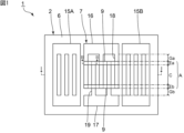
- FIG. 1 is a schematic plan view of an elastic wave device according to a first preferred embodiment of the present invention.
- FIG. 2 is a schematic cross-sectional view taken along line II in FIG.
- FIG. 3 is a schematic cross-sectional view taken along line II-II in FIG.
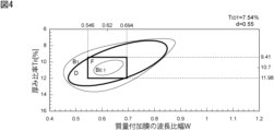
- FIG. 4 is a diagram showing the relationship between the wavelength ratio width W and the thickness ratio TR of the mass-adding film when the Al-equivalent normalized thickness T IDT of the electrode finger portion is 7.54% and the duty ratio d is 0.55, and the magnitude of the ripple caused by the transverse mode is 1 dB or 0.1 dB .
- FIG. 1 is a schematic plan view of an elastic wave device according to a first preferred embodiment of the present invention.
- FIG. 2 is a schematic cross-sectional view taken along line II in FIG.
- FIG. 3 is a schematic cross-sectional view taken along line II-II in FIG.
- FIG. 4 is a diagram showing the relationship between the wavelength ratio width W and the thickness ratio TR
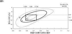
- FIG. 5 is a diagram showing the relationship between the wavelength ratio width W and the thickness ratio TR of the mass-adding film when the Al-equivalent normalized thickness T IDT of the electrode finger portion is 6.17% and the duty ratio d is 0.55, and the magnitude of the ripple caused by the transverse mode is 1 dB or 0.1 dB .
- FIG. 6 is a diagram showing the relationship between the wavelength ratio width W and the thickness ratio TR of the mass-adding film when the Al-equivalent normalized thickness T IDT of the electrode finger portion is 5.22% and the duty ratio d is 0.55, and the magnitude of the ripple caused by the transverse mode is 1 dB or 0.1 dB .
- FIG. 6 is a diagram showing the relationship between the wavelength ratio width W and the thickness ratio TR of the mass-adding film when the Al-equivalent normalized thickness T IDT of the electrode finger portion is 5.22% and the duty ratio d is 0.55, and the magnitude of the ripple caused by the transverse mode is 1 dB or 0.1
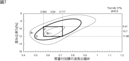
- FIG. 7 is a diagram showing the relationship between the wavelength ratio width W and the thickness ratio TR of the mass-adding film when the Al-equivalent normalized thickness T IDT of the electrode finger portion is 6.17% and the duty ratio d is 0.5, and the magnitude of the ripple caused by the transverse mode is 1 dB or 0.1 dB .
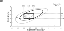
- FIG. 8 is a diagram showing the relationship between the wavelength ratio width W and the thickness ratio TR of the mass-adding film when the Al-equivalent normalized thickness T IDT of the electrode finger portion is 6.17% and the duty ratio d is 0.6, and the magnitude of the ripple caused by the transverse mode is 1 dB or 0.1 dB .
- FIG. 9(a) is a diagram showing the occurrence of ripples in the attenuation-frequency characteristic of the filter device
- Fig. 9(b) is a diagram showing the impedance-frequency characteristic of an elastic wave resonator used in the filter device whose attenuation-frequency characteristic is shown in Fig. 9(a)
- Fig. 9(c) is a diagram showing the return loss of the elastic wave resonator whose impedance-frequency characteristic is shown in Fig. 9(b).
- FIG. 10 is a graph showing the relationship between the magnitude of ripples as return loss in a first acoustic wave resonator and the magnitude of ripples in the attenuation frequency characteristics of a filter device.
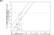
- FIG. 11 is a graph showing the relationship between the magnitude of ripples as return loss in the second acoustic wave resonator and the magnitude of ripples in the attenuation frequency characteristics of the filter device.
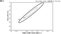
- FIG. 12 is a diagram showing the relationship between the wavelength ratio width W and the thickness ratio TR of the mass-adding film in which the magnitude of the ripple caused by the transverse mode is 1 dB or 0.3 dB when the piezoelectric layer is made of lithium tantalate, the Al-equivalent normalized thickness T IDT of the electrode finger portion is 7.83%, and the duty ratio d is 0.5, in the case where the resonant frequency is 1 GHz or less.
- FIG. 12 is a diagram showing the relationship between the wavelength ratio width W and the thickness ratio TR of the mass-adding film in which the magnitude of the ripple caused by the transverse mode is 1 dB or 0.3 dB when the piezoelectric layer is made of lithium tantalate, the Al-equivalent normalized thickness T IDT of the electrode finger
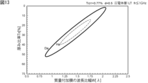
- FIG. 13 is a diagram showing the relationship between the wavelength ratio width W and the thickness ratio TR of the mass-adding film in which the magnitude of the ripple caused by the transverse mode is 1 dB or 0.3 dB when the piezoelectric layer is made of lithium tantalate, the Al-equivalent normalized thickness T IDT of the electrode finger portion is 3.77%, and the duty ratio d is 0.5, in the case where the resonant frequency is 1 GHz or less.
- Fig. 14 is a diagram showing the relationship between the wavelength ratio width W and the thickness ratio TR of the mass-adding film in which the magnitude of the ripple caused by the transverse mode is 1 dB or 0.3 dB when the piezoelectric layer is made of lithium tantalate, the Al-equivalent normalized thickness T IDT of the electrode finger portion is 7.83%, and the duty ratio d is 0.7, in the case where the resonant frequency is 1 GHz or less.
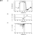
- Fig. 15(a) is a diagram showing the occurrence of ripples in the attenuation frequency characteristic of a low-band filter device.
- FIG. 15(b) is a diagram showing the impedance frequency characteristic of an elastic wave resonator used in the filter device whose attenuation frequency characteristic is shown in Fig. 15(a).
- Fig. 15(c) is a diagram showing the return loss of the elastic wave resonator whose impedance frequency characteristic is shown in Fig. 15(b).
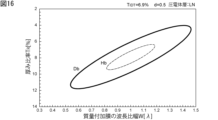
- FIG. 16 is a diagram showing the relationship between the wavelength ratio width W and the thickness ratio TR of the mass addition film in which the magnitude of the ripple caused by the transverse mode is 1 dB or 0.2 dB when the piezoelectric layer is made of lithium niobate, the Al-equivalent normalized thickness T IDT of the electrode finger portion is 6.9%, and the duty ratio d is 0.5.
- FIG. 17 is a diagram showing the relationship between the wavelength ratio width W and the thickness ratio TR of the mass addition film in which the magnitude of the ripple caused by the transverse mode is 1 dB or 0.2 dB when the piezoelectric layer is made of lithium niobate, the Al-equivalent normalized thickness T IDT of the electrode finger portion is 13.7%, and the duty ratio d is 0.5.
- FIG. 17 is a diagram showing the relationship between the wavelength ratio width W and the thickness ratio TR of the mass addition film in which the magnitude of the ripple caused by the transverse mode is 1 dB or 0.2 dB when the piezoelectric layer is made of lithium niobate, the Al-equivalent normalized thickness T IDT of the electrode finger portion is 13.7%, and the duty ratio d is 0.5.
- FIG. 18 is a diagram showing the relationship between the wavelength ratio width W and the thickness ratio TR of the mass addition film in which the magnitude of the ripple caused by the transverse mode is 1 dB or 0.2 dB when the piezoelectric layer is made of lithium niobate, the Al-equivalent normalized thickness T IDT of the electrode finger portion is 13.7%, and the duty ratio d is 0.7.
- FIG. 1 is a schematic plan view of an elastic wave device according to a first embodiment of the present invention.
- FIG. 2 is a schematic cross-sectional view taken along line I-I in FIG. 1.
- FIG. 3 is a schematic cross-sectional view taken along line II-II in FIG. 1. Note that a dielectric film, which will be described later, is omitted in FIG. 1.
- the elastic wave device 1 has a piezoelectric substrate 2.
- the piezoelectric substrate 2 includes a support substrate 3, a high acoustic velocity film 4 as a high acoustic velocity material layer, a low acoustic velocity film 5, and a piezoelectric layer 6.
- the high acoustic velocity film 4 is provided on the support substrate 3.
- the low acoustic velocity film 5 is provided on the high acoustic velocity film 4.
- the piezoelectric layer 6 is provided on the low acoustic velocity film 5.
- the piezoelectric layer 6 is provided indirectly on the high acoustic velocity material layer via the low acoustic velocity film 5.
- the piezoelectric layer 6 may also be provided directly on the high acoustic velocity material layer.
- the piezoelectric layer 6 is made of, for example, lithium tantalate such as LiTaO3 .
- a certain member being made of a certain material includes the case where a small amount of impurities are contained to the extent that the electrical characteristics of the acoustic wave device are not significantly deteriorated.
- An IDT electrode 7 is provided on the piezoelectric layer 6. An AC voltage is applied to the IDT electrode 7 to excite an acoustic wave.
- the high acoustic velocity material layer in the piezoelectric substrate 2 is a layer with a relatively high acoustic velocity. More specifically, the acoustic velocity of the bulk waves propagating through the high acoustic velocity material layer is higher than the acoustic velocity of the elastic waves propagating through the piezoelectric layer 6.
- the high acoustic velocity material layer is the high acoustic velocity film 4.
- the low acoustic velocity film 5 is a film with a relatively low acoustic velocity. More specifically, the acoustic velocity of the bulk waves propagating through the low acoustic velocity film 5 is lower than the acoustic velocity of the bulk waves propagating through the piezoelectric layer 6.
- the IDT electrode 7 has a first bus bar 16 and a second bus bar 17, a plurality of first electrode fingers 18 and a plurality of second electrode fingers 19.
- the first bus bar 16 and the second bus bar 17 face each other.
- One end of each of the first electrode fingers 18 is connected to the first bus bar 16.
- One end of each of the second electrode fingers 19 is connected to the second bus bar 17.
- the first electrode fingers 18 and the second electrode fingers 19 are interdigitated with each other.
- the first electrode fingers 18 and the second electrode fingers 19 are connected to different potentials.
- a dielectric film 8 is provided on the piezoelectric layer 6 so as to cover the IDT electrode 7.
- silicon oxide is used as the material for the dielectric film 8.
- the material for the dielectric film 8 is not limited to the above.
- the IDT 27 is formed by stacking the IDT electrode 7 and the dielectric film 8.
- the portion where the first electrode fingers 18 of the IDT electrode 7 and the dielectric film 8 are stacked is the first electrode finger portion 28 of the IDT 27.
- the portion where the second electrode fingers 19 of the IDT electrode 7 and the dielectric film 8 are stacked is the second electrode finger portion 29 of the IDT 27.
- the first electrode finger portion 28 and the second electrode finger portion 29 of the IDT 27 may be simply referred to as the electrode finger portion.
- the first electrode fingers 18 and the second electrode fingers 19 of the IDT electrode 7 may be simply referred to as the electrode fingers.
- Each electrode finger portion of the IDT 27 has multiple electrode finger layers.
- the multiple electrode finger layers include a metal layer 27a and a dielectric layer 27b.
- the metal layer 27a is a layer included in the IDT electrode 7.
- the metal layer 27a is the electrode finger portion of the IDT electrode 7.
- the IDT electrode 7 is made of a laminated metal film.
- the IDT electrode 7 includes an Al layer and multiple Ti layers. Therefore, each electrode finger portion of the IDT 27 includes multiple metal layers 27a.
- the material and layer structure of the IDT electrode 7 are not limited to the above.
- the IDT electrode 7 may be made of a single layer of metal film. In this case, each electrode finger portion of the IDT 27 includes only one metal layer 27a.
- the dielectric layer 27b of the IDT 27 is a layer that is included in the dielectric film 8. Note that the dielectric film 8 does not necessarily have to be provided. In this case, the IDT 27 is the IDT electrode 7. Therefore, the electrode finger layer may have only the metal layer 27a. Each electrode finger portion needs to include at least one electrode finger layer.
- a pair of reflectors 15A and 15B are provided on the piezoelectric layer 6.
- the reflectors 15A and 15B face each other across the IDT 27 in a direction perpendicular to the electrode finger portion extension direction.
- the direction perpendicular to the electrode finger portion extension direction and the elastic wave propagation direction are parallel.
- the same material as the IDT electrode 7 can be used for each reflector.
- the elastic wave device 1 of this embodiment is a surface acoustic wave resonator.
- the elastic wave device 1 can be suitably used, for example, in a mid-high band (MHB) filter device.
- the mid-high band frequency band is 1.7 GHz to 2.7 GHz.
- the intersection region A has a central region C and a pair of edge regions.
- the pair of edge regions is a first edge region Ea and a second edge region Eb.
- the first edge region Ea and the second edge region Eb are arranged to face each other across the central region C in the extension direction of the electrode finger portions.
- the first edge region Ea is located on the first bus bar 16 side.
- the second edge region Eb is located on the second bus bar 17 side.
- a pair of mass-adding films 9 are provided in a pair of edge regions. Specifically, one of the pair of mass-adding films 9 is provided in the first edge region Ea. The other of the pair of mass-adding films 9 is provided in the second edge region Eb.
- Each mass-adding film 9 has a band-like shape. More specifically, each mass-adding film 9 is provided continuously so as to overlap with a plurality of electrode finger portions and the regions between the electrode finger portions in a plan view.
- a plan view refers to viewing the acoustic wave device from a direction corresponding to the top in FIG. 2. In FIG. 2, for example, of the piezoelectric layer 6 side and the dielectric film 8 side, the dielectric film 8 side is the top.
- a low sound speed region is a region in which the sound speed is lower than the sound speed in the central region C.
- the central region C and a pair of low sound velocity regions are arranged in this order from inside to outside in the direction of extension of the electrode finger portion. This allows the piston mode to be established and the transverse mode to be suppressed.
- tantalum oxide such as Ta 2 O 5 is used as the material of the mass adding film 9.
- the material of the mass adding film 9 is not limited to the above.
- FIG. 3 a cross section in the first edge region Ea is shown.
- the mass-adding film 9 is provided between the IDT electrode 7 and the dielectric film 8.
- the mass-adding film 9 is also provided between the IDT electrode 7 and the dielectric film 8.
- the IDT 27 does not include a mass-adding film 9.
- the first electrode finger 18 and the second electrode finger 19 of the IDT electrode 7 each have a first surface 7a, a second surface 7b, and a side surface 7c.
- the first surface 7a and the second surface 7b face each other.
- the second surface 7b is located on the piezoelectric layer 6 side.
- the side surface 7c is connected to the first surface 7a and the second surface 7b.
- the side surface 7c extends at an angle with respect to the normal direction of the second surface 7b.
- the side surface 7c may extend parallel to the normal direction of the second surface 7b.
- the dielectric film 8 is provided across the first surface 7a and side surface 7c of the electrode fingers. In each edge region, the dielectric film 8 is indirectly provided on the electrode fingers via a mass-adding film 9.
- the dielectric layer 27b in the electrode finger portion of the IDT 27 is the portion of the dielectric film 8 that is provided directly or indirectly on the first surface 7a of the electrode fingers.
- the wavelength defined by the electrode finger pitch is defined as ⁇ .
- the electrode finger pitch refers to the distance between the centers of adjacent electrode fingers in a direction perpendicular to the electrode finger extension direction.
- the duty ratio of the IDT 27 is defined as d.
- the duty ratio d of the IDT 27 is the same as the duty ratio of the IDT electrode 7. More specifically, the duty ratio d of the IDT 27 is the duty ratio based on the second surface 7b of each electrode finger in the IDT electrode 7.
- the wavelength ratio width W is defined as the value obtained by dividing the dimension of the mass addition film 9 along the electrode finger extension direction by the wavelength ⁇ .
- the product of the density and thickness of any layer divided by the density and wavelength ⁇ of Al is defined as the Al-converted normalized thickness of the layer.
- the total of the Al-converted normalized thicknesses of the electrode finger layers is defined as T IDT [%], which is the Al-converted normalized thickness of the electrode finger portion.
- T IDT [%] the Al-converted normalized thickness of the electrode finger portion.
- the density of the k-th electrode finger layer from the piezoelectric layer 6 side is ⁇ k
- the thickness is t k
- the Al-converted normalized thickness is T k [%]
- the density of Al is ⁇ Al
- the Al-converted normalized thickness T k of each electrode finger layer is ⁇ ( ⁇ k t k )/( ⁇ Al ⁇ ) ⁇ 100 [%].
- ⁇ Al is 2.69 g/cm 3 when the significant digits are three.
- the Al-equivalent normalized thickness of the mass adding film 9 is Tm [%]
- the thickness ratio of the Al-equivalent normalized thickness Tm of the mass adding film 9 to the Al-equivalent normalized thickness TIDT of the electrode finger portion divided by 3.15 is TR [%]
- TR (1/3.15) x ( Tm / TIDT ) x 100 [%].
- the Al-equivalent normalized thickness Tm of the mass adding film 9 corresponds to the value obtained by substituting the density ⁇ k and thickness tk of the mass adding film 9 into the Al-equivalent normalized thickness Tk of the electrode finger portion layer, ⁇ ( ⁇ k ⁇ tk )/( ⁇ Al ⁇ ) ⁇ x 100.
- the elastic wave device 1 of this embodiment has at least one of a first feature and a second feature.
- the relationship between the wavelength ratio width W and the thickness ratio TR is expressed in an xy plane. More specifically, in the xy plane, the value of x corresponds to the value of the wavelength ratio width W.
- the value of y corresponds to the value of the thickness ratio TR .
- the first feature is as follows. 1) The piezoelectric layer 6 is made of lithium tantalate. 2) The resonant frequency of the elastic wave device 1 is higher than 1 GHz.
- the wavelength ratio width W and the thickness ratio TR are values within a range of an ellipse expressed by setting ⁇ to be equal to or greater than 0° and less than 360° in the following formulas 1 and 2, and within the inside of the ellipse.
- the second feature is as follows. 1) Piezoelectric layer 6 is made of lithium tantalate. 2) The resonant frequency of elastic wave device 1 is higher than 1 GHz. 3) The wavelength ratio width W and thickness ratio T R of mass adding film 9 are within the following ranges. That is, the wavelength ratio width W is 0.88 ⁇ 0.0101 ⁇ T IDT 2 ⁇ 0.1677 ⁇ T IDT +1.3201 +0.4 ⁇ (d ⁇ 0.55) ⁇ W ⁇ 1.12 ⁇ 0.0101 ⁇ T IDT 2 ⁇ 0.1677 ⁇ T IDT +1.3201 +0.4 ⁇ (d ⁇ 0.55) ⁇ . The thickness ratio T R is 0.88 ⁇ 10.7 ⁇ T R ⁇ 1.12 ⁇ 10.7.
- the transverse mode can be more reliably suppressed. More specifically, in the elastic wave device 1, the magnitude of the ripple in the frequency characteristics caused by the transverse mode can be more reliably suppressed to 1 dB or less. The details of this are described below.
- transverse modes include a variety of modes, such as 1st to 11th orders. According to the present invention, the magnitude of the largest ripple in the frequency characteristics caused by transverse modes can be more reliably suppressed to 1 dB or less.
- the transverse mode can be suppressed by setting a predetermined relationship between the thickness ratio TR of the Al-equivalent normalized thickness Tm of the mass adding film 9 to the Al-equivalent normalized thickness TIDT of the electrode finger portion divided by 3.15 and the wavelength ratio width W of the mass adding film 9.
- the inventors have derived a relationship and range between the wavelength ratio width W and the thickness ratio TR that can suppress the magnitude of the ripple caused by the transverse mode in the frequency characteristics to 1 dB or less in the acoustic wave device.
- the design parameters of the acoustic wave device related to this derivation are as follows:
- the thickness ratio TR was changed as described above by changing the thickness of the mass-adding film according to the Al-equivalent normalized thickness T IDT . Each time the thickness ratio TR and the wavelength ratio width W were changed, the return loss was measured and the magnitude of the ripple caused by the transverse mode was obtained.
- Fig. 4 is a diagram showing the relationship between the wavelength ratio width W and the thickness ratio TR of the mass-adding film, where the magnitude of the ripple caused by the transverse mode is 1 dB or 0.1 dB when the Al-equivalent normalized thickness T IDT of the electrode finger portion is 7.54% and the duty ratio d is 0.55.
- the value of x in the xy plane corresponds to the value of the wavelength ratio width W.
- the value of y corresponds to the value of the thickness ratio TR .
- the solid line B1 indicates a combination of the wavelength ratio width W and the thickness ratio TR where the magnitude of the ripple due to the transverse mode in the frequency characteristics of the elastic wave device is 1 dB.
- the magnitude of the ripple due to the transverse mode is 1 dB or less.
- Equation 4 shows an ellipse D expressed by Equations 1 and 2.
- This ellipse D is located within the range surrounded by solid line B1 .
- the first characteristic is that the wavelength ratio width W and the thickness ratio TR are values within the ellipse D and the range inside the ellipse D. Therefore, by having elastic wave device 1 with the first characteristic, the magnitude of the ripple caused by the transverse mode can be more reliably suppressed to 1 dB or less.
- the Al-equivalent normalized thickness T IDT of the electrode finger portion and the duty ratio d are different, the condition under which the magnitude of the ripple caused by the transverse mode is 1 dB or less also differs. Therefore, the Al-equivalent normalized thickness T IDT of the electrode finger portion and the duty ratio d are varied to find the condition under which the magnitude of the ripple caused by the transverse mode is 1 dB or less in each case.
- the ellipse derived in this way is the ellipse D represented by the formulas 1 and 2.
- the magnitude of the ripple caused by the transverse mode can be made 1 dB or less in any case of the Al-equivalent normalized thickness T IDT of the electrode finger portion and the duty ratio d.
- range F This range F is located within the range surrounded by solid line B1 .
- the wavelength ratio width W and thickness ratio TR have values within this range F, which is characteristic 2. Therefore, by having elastic wave device 1 with the second characteristic, the magnitude of ripples caused by the transverse mode can be more reliably suppressed to 1 dB or less.
- range F is a range of ⁇ 12% centered on the combination of wavelength ratio width W and thickness ratio TR at which the transverse mode is most suppressed.
- the wavelength ratio width W and thickness ratio TR at which the transverse mode is most suppressed vary depending on the Al-equivalent normalized thickness T IDT of the electrode finger portion and the duty ratio d.
- the wavelength ratio width W and thickness ratio TR at which the ripple caused by the transverse mode is most suppressed were determined for each case.
- the wavelength ratio width W in the range F derived from this is 0.88 ⁇ 0.0101 ⁇ T IDT 2 ⁇ 0.1677 ⁇ T IDT +1.3201 +0.4 ⁇ (d ⁇ 0.55) ⁇ W ⁇ 1.12 ⁇ 0.0101 ⁇ T IDT 2 ⁇ 0.1677 ⁇ T IDT +1.3201 +0.4 ⁇ (d ⁇ 0.55) ⁇ .
- the thickness ratio T R derived as above is 0.88 ⁇ 10.7 ⁇ T R ⁇ 1.12 ⁇ 10.7, which is a constant range. Therefore, by having the wavelength ratio width W and the thickness ratio T R within the range F, the magnitude of the ripple caused by the transverse mode can be made 1 dB or less regardless of the Al-equivalent normalized thickness T IDT of the electrode finger portion and the duty ratio d.
- the solid line B0.1 shows a combination of wavelength ratio width W and thickness ratio TR where the magnitude of ripple caused by the transverse mode is 0.1 dB.
- the magnitude of ripple caused by the transverse mode can be suppressed to 0.1 dB or less.
- the wavelength ratio width W and thickness ratio TR of the mass addition film 9 are within the range F, the wavelength ratio width W and thickness ratio TR are close to the solid line B0.1 or are within the range surrounded by the solid line B0.1 . Therefore, when the elastic wave device 1 has the above-mentioned feature 2, the transverse mode can be suppressed more reliably and effectively.
- Figures 5 to 8 show cases where the Al-equivalent normalized thickness T IDT of the electrode finger portion and the duty ratio d are under conditions other than those in Figure 4.
- solid lines B 1 and B 0.1 an ellipse D, and a range F are also shown.
- Fig. 5 is a diagram showing the relationship between the wavelength ratio width W and thickness ratio TR of the mass addition film when the Al-equivalent standardized thickness T IDT of the electrode finger portion is 6.17% and the duty ratio d is 0.55, and the magnitude of the ripple caused by the transverse mode is 1 dB or 0.1 dB.
- Fig. 6 is a diagram showing the relationship between the wavelength ratio width W and thickness ratio TR of the mass addition film when the Al-equivalent standardized thickness T IDT of the electrode finger portion is 5.22% and the duty ratio d is 0.55, and the magnitude of the ripple caused by the transverse mode is 1 dB or 0.1 dB.
- FIG. 7 is a diagram showing the relationship between the wavelength ratio width W and thickness ratio TR of the mass addition film when the Al-equivalent standardized thickness T IDT of the electrode finger portion is 6.17% and the duty ratio d is 0.5, and the magnitude of the ripple caused by the transverse mode is 1 dB or 0.1 dB.
- FIG. 8 is a diagram showing the relationship between the wavelength ratio width W and the thickness ratio TR of the mass-adding film when the Al-equivalent normalized thickness T IDT of the electrode finger portion is 6.17% and the duty ratio d is 0.6, and the magnitude of the ripple caused by the transverse mode is 1 dB or 0.1 dB .
- the wavelength ratio width W of the mass adding film 9 as the value of x and the thickness ratio TR as the value of y are ellipse D and values within the range inside ellipse D, so that the magnitude of the ripple caused by the transverse mode can be more reliably suppressed to 1 dB or less.
- ellipse D is an ellipse expressed by setting ⁇ to be equal to or greater than 0° and less than 360° in formulas 1 and 2.
- the magnitude of the ripple caused by the transverse mode can be more reliably suppressed to 1 dB or less by having the wavelength ratio width W and the thickness ratio TR within the range F.
- the wavelength ratio width W may be 0.88 ⁇ 0.0101 ⁇ T IDT 2 ⁇ 0.1677 ⁇ T IDT +1.3201 +0.4 ⁇ (d ⁇ 0.55) ⁇ W ⁇ 1.12 ⁇ 0.0101 ⁇ T IDT 2 ⁇ 0.1677 ⁇ T IDT +1.3201 +0.4 ⁇ (d ⁇ 0.55) ⁇ .
- the thickness ratio TR may be 0.88 ⁇ 10.7 ⁇ T R ⁇ 1.12 ⁇ 10.7.
- the transverse mode is most suppressed when the wavelength ratio width W and thickness ratio TR of the mass adding film 9 are as follows: From these results, the range F is derived.
- the elastic wave device according to the present invention is used, for example, as an elastic wave resonator in a filter device.
- transverse modes can be more reliably suppressed. This makes it possible to more reliably suppress ripples in the frequency characteristics of the filter device. This is described in detail below.
- Figure 9(a) is a diagram showing the occurrence of ripples in the attenuation frequency characteristics of a filter device.
- Figure 9(b) is a diagram showing the impedance frequency characteristics of an elastic wave resonator used in the filter device whose attenuation frequency characteristics are shown in Figure 9(a).
- Figure 9(c) is a diagram showing the return loss of an elastic wave resonator whose impedance frequency characteristics are shown in Figure 9(b).
- multiple ripples occur in the attenuation frequency characteristic of the filter device. Note that multiple ripples occur within the passband of the filter device. At the frequencies where these ripples occur, ripples also occur in the impedance frequency characteristic of the elastic wave resonator, as shown in FIG. 9(b). It can therefore be seen that unwanted waves generated in the elastic wave resonator used in the filter device cause ripples in the attenuation frequency characteristic of the filter device. Note that the multiple unwanted waves shown in FIG. 9(b) are in transverse mode. It can be seen that the larger the ripples caused by the transverse mode as the return loss of the elastic wave resonator shown in FIG. 9(c), the larger the ripples in the filter device shown in FIG. 9(a).
- the relationship between the ripples in the frequency characteristics of the elastic wave resonator and the filter device is described in more detail below.
- a plurality of elastic wave resonators and a plurality of filter devices were prepared.
- the magnitude of the ripples caused by the transverse mode as return loss was adjusted. This caused the magnitude of the ripples to differ between the elastic wave resonators.
- Each filter device includes one of these elastic wave resonators and another elastic wave resonator.
- the elastic wave resonators with the adjusted ripple magnitudes were arranged in two ways in the filter device. In the following, the elastic wave resonator arranged in one way is referred to as the first elastic wave resonator.
- the elastic wave resonator arranged in the other way is referred to as the second elastic wave resonator.
- the first elastic wave resonator is a series arm resonator in the filter device.
- the second elastic wave resonator is a parallel arm resonator in the filter device.
- FIG. 10 is a diagram showing the relationship between the magnitude of ripples as return loss in a first elastic wave resonator and the magnitude of ripples in the attenuation frequency characteristics of a filter device.
- FIG. 11 is a diagram showing the relationship between the magnitude of ripples as return loss in a second elastic wave resonator and the magnitude of ripples in the attenuation frequency characteristics of a filter device.
- Each plot in FIG. 10 shows the relationship between the magnitude of ripple in the return loss of each first acoustic wave resonator and the magnitude of ripple in the attenuation frequency characteristics of each filter device. Based on these plots, the relationship between the magnitude of ripple in the frequency characteristics of the first acoustic wave resonator and the filter device was derived. This relationship is shown by the solid straight line in FIG. 10.
- the dashed line in Figure 10 is a line that passes through any of the plots and has the largest intercept when the slope is the same as the solid line.
- the dashed line shows the relationship in which the ripple in the attenuation frequency characteristic of the filter device is assumed to be largest relative to the ripple as the return loss in the first acoustic wave resonator.
- the magnitude of the ripple in the attenuation frequency characteristic be 0.5 dB or less.
- the magnitude of the ripple as the return loss in the first acoustic wave resonator is 1.8 dB or less, so that the magnitude of the ripple in the attenuation frequency characteristic of the filter device can be 0.5 dB or less.
- the straight solid line in FIG. 11 indicates the relationship between the magnitude of ripples in the frequency characteristics of the second elastic wave resonator and the filter device.
- the slope of the solid line in FIG. 11 is greater than the slope of the solid line in FIG. 10. In this way, the relationship between the magnitude of ripples in the elastic wave resonator and the filter device differs depending on the arrangement of the elastic wave resonator, etc.
- the dashed dotted line in FIG. 11 indicates the relationship in which the ripples in the attenuation frequency characteristics of the filter device are assumed to be largest relative to the ripples as return loss in the second elastic wave resonator.
- the magnitude of the ripples as return loss in the second elastic wave resonator is 1 dB or less, the magnitude of the ripples in the attenuation frequency characteristics of the filter device can be 0.5 dB or less.
- the magnitude of ripple in the attenuation frequency characteristics of the filter device can be more reliably set to 0.5 dB or less.
- the magnitude of ripple caused by the transverse mode can be more reliably suppressed to 1 dB or less. Therefore, when the elastic wave device 1 is used in a filter device, the ripple in the attenuation frequency characteristics of the filter device can also be more reliably suppressed to 0.5 dB or less. Therefore, deterioration of the filter characteristics of the filter device can be suppressed.
- a pair of gap regions are disposed between the intersection region A and the pair of bus bars.
- the pair of gap regions are a first gap region Ga and a second gap region Gb.
- the first gap region Ga is located on the side of the first bus bar 16.
- the second gap region Gb is located on the side of the second bus bar 17.
- the first gap region Ga of the multiple first electrode fingers 18 and multiple second electrode fingers 19, only the multiple first electrode fingers 18 are provided. This forms a high acoustic velocity region in the first gap region Ga.
- the high acoustic velocity region refers to a region where the acoustic velocity is higher than the acoustic velocity in the central region C.
- a high acoustic velocity region is formed in the second gap region Gb.
- a central region C In the direction of extension of the electrode fingers, from inside to outside, a central region C, a pair of low acoustic velocity regions, and a pair of high acoustic velocity regions are arranged in this order. This makes it possible to more reliably suppress transverse modes.
- each mass-adding film 9 is provided in each edge region. It is sufficient that the mass-adding film 9 is provided in at least one of the first edge region Ea and the second edge region Eb. However, it is preferable that the mass-adding film 9 is provided in both the first edge region Ea and the second edge region Eb. This makes it possible to more reliably and effectively suppress the transverse mode.
- the mass-adding film 9 is provided between the IDT electrode 7 and the dielectric film 8.
- the mass-adding film 9, the IDT electrode 7, and the dielectric film 8 may be stacked in this order from the piezoelectric layer 6 side.
- the IDT electrode 7, the dielectric film 8, and the mass-adding film 9 may be stacked in this order from the piezoelectric layer 6 side.
- the piezoelectric substrate 2 of the elastic wave device 1 is a laminated substrate.
- Examples of materials for each layer in the piezoelectric substrate 2 are as follows:
- the material of the piezoelectric layer 6 is lithium tantalate, such as LiTaO3 .
- the low acoustic velocity film 5 may be made of a dielectric material such as glass, silicon oxide, silicon oxynitride, lithium oxide, tantalum oxide, or a compound of silicon oxide with fluorine, carbon, or boron added, or a material that contains the above materials as its main component.
- the term "main component” refers to a component that accounts for more than 50 wt%.
- the above main component material may be in any of the following states: single crystal, polycrystalline, or amorphous, or a mixture of these.
- the high acoustic velocity material layer is the high acoustic velocity film 4.
- high acoustic velocity materials include piezoelectric materials such as aluminum nitride, lithium tantalate, lithium niobate, and quartz crystal, ceramics such as alumina, sapphire, magnesia, silicon nitride, silicon carbide, zirconia, cordierite, mullite, steatite, forsterite, spinel, and sialon, dielectric materials such as aluminum oxide, silicon oxynitride, DLC (diamond-like carbon), and diamond, and semiconductors such as silicon, or materials mainly composed of the above materials.
- the spinel includes aluminum compounds containing one or more elements selected from Mg, Fe, Zn, Mn, and the like, and oxygen.
- Examples of the spinel include MgAl 2 O 4 , FeAl 2 O 4 , ZnAl 2 O 4 , and MnAl 2 O 4 .
- Materials for the support substrate 3 include, for example, piezoelectric materials such as aluminum nitride, lithium tantalate, lithium niobate, and quartz; ceramics such as alumina, sapphire, magnesia, silicon nitride, silicon carbide, zirconia, cordierite, mullite, steatite, and forsterite; dielectric materials such as diamond and glass; semiconductors such as silicon and gallium nitride; resins; or materials containing the above materials as their main components.
- piezoelectric materials such as aluminum nitride, lithium tantalate, lithium niobate, and quartz
- ceramics such as alumina, sapphire, magnesia, silicon nitride, silicon carbide, zirconia, cordierite, mullite, steatite, and forsterite
- dielectric materials such as diamond and glass
- semiconductors such as silicon and gallium nitride
- resins or materials containing the above materials as their main
- a high acoustic velocity film 4 as a high acoustic velocity material layer, a low acoustic velocity film 5, and a piezoelectric layer 6 are laminated in this order. This allows the energy of the elastic waves to be effectively trapped on the piezoelectric layer 6 side.
- the piezoelectric substrate may be a layered substrate of a support substrate, a high acoustic velocity film, and a piezoelectric layer.
- the high acoustic velocity material layer may be a high acoustic velocity support substrate.
- the piezoelectric substrate may be a layered substrate of a high acoustic velocity support substrate, a low acoustic velocity film, and a piezoelectric layer, or a layered substrate of a high acoustic velocity support substrate and a piezoelectric layer. Even in these cases, the energy of the elastic wave can be effectively trapped on the piezoelectric layer side.
- Table 1 shows examples of metal and dielectric materials, and the density of each material.
- the metals listed in Table 1 may be used as the material for metal layer 27a in IDT 27 shown in FIG. 3.
- the dielectrics listed in Table 1 may be used as the material for dielectric layer 27b.
- the dielectrics listed in Table 1 may be used for mass-adding film 9. Note that the metal material used for metal layer 27a and the dielectric material used for dielectric layer 27b or mass-adding film 9 may contain trace amounts of different materials.
- the Al layer may contain a trace amount of Cu.
- the density of the material of the mass-adding film 9 is higher than the density of the dielectric layer 27b of the electrode finger portion. This allows the thickness of the mass-adding film 9 to be thinner than the thickness of the dielectric film 8. This allows the mass-adding film 9 to be more reliably covered by the dielectric film 8.
- the frequency of the elastic wave device 1 can be adjusted by trimming the surface of the dielectric film 8 and adjusting the thickness of the dielectric film 8.
- the mass-adding film 9 can be more reliably covered by the dielectric film 8. This makes it possible to prevent the mass-adding film 9 from being trimmed when trimming the dielectric film 8. This makes it possible to suppress the effect of trimming on the difference between the sound velocity in the central region C shown in FIG. 1 and the sound velocity in a pair of edge regions. This makes it possible to effectively suppress the transverse mode.
- intersection width is 10 ⁇ or more. In this case, the transverse mode can be more reliably and suitably suppressed. It is preferable that the intersection width is 30 ⁇ or less. This makes it possible to prevent the elastic wave device 1 from becoming too large.
- the edge portion of the mass-adding film 9 located in the first edge region Ea on the first bus bar 16 side overlaps with the tip of the second electrode finger 19 in a planar view.
- the edge portion of the mass-adding film 9 located in the first edge region Ea on the first bus bar 16 side does not have to overlap with the tip of the second electrode finger 19 in a planar view. In this case, the edge portion of the mass-adding film 9 on the first bus bar 16 side only needs to be located in the first edge region Ea.
- the distance in the electrode finger extension direction between the edge portion of the mass-adding film 9 located in the first edge region Ea on the first bus bar 16 side and the tip of the second electrode finger 19 in a planar view is 0.1 ⁇ or less.
- the edge portion of the mass adding film 9 located in the second edge region Eb on the second bus bar 17 side overlaps with the tip of the first electrode finger 18 in a planar view.
- the edge portion of the mass adding film 9 located in the second edge region Eb on the second bus bar 17 side does not have to overlap with the tip of the first electrode finger 18 in a planar view. In this case, it is sufficient that the edge portion of the mass adding film 9 on the second bus bar 17 side is located in the second edge region Eb.
- the distance in the electrode finger extension direction between the edge portion of the mass adding film 9 located in the second edge region Eb on the second bus bar 17 side and the tip of the first electrode finger 18 in a planar view is 0.1 ⁇ or less.
- the relationship between the thickness and duty ratio of the electrode finger portion, which can suppress the transverse mode, and the wavelength ratio width W and thickness ratio TR of the mass-adding film differs depending on the resonant frequency of the elastic wave device and the material of the piezoelectric layer.
- the piezoelectric layer 14 is made of lithium tantalate.
- the resonant frequency of the elastic wave device 1 is higher than 1 GHz.
- the wavelength ratio width W and the thickness ratio TR may be within the range of the ellipse expressed by setting ⁇ to be equal to or greater than 0° and less than 360° in the above formulas 1 and 2, and within the range inside the ellipse.
- the wavelength ratio width W and the thickness ratio TR may be within the above range F. This makes it possible to more reliably suppress the transverse mode.
- a second embodiment and a third embodiment will be described, which show examples in which the piezoelectric layer is made of lithium tantalate and the resonant frequency of the elastic wave device is 1 GHz or less, and an example in which the piezoelectric layer is made of lithium niobate.
- the stacked configurations in the second and third embodiments are similar to the stacked configuration in the first embodiment. Therefore, the symbols and drawings used in the description of the first embodiment will be used in the description of the second and third embodiments.
- the second embodiment differs from the first embodiment in that the resonant frequency of the elastic wave device is 1 GHz or less.
- the elastic wave device of the second embodiment has a piezoelectric substrate 2 and an IDT 27, as shown with reference to FIG. 2. Note that it is sufficient that the piezoelectric substrate 2 has at least a high acoustic velocity material layer and a piezoelectric layer 6.
- a mass-adding film 9 is provided in each of the first edge region Ea and the second edge region Eb. However, it is sufficient that the mass-adding film 9 is provided in at least one of the first edge region Ea and the second edge region Eb.
- the piezoelectric layer 6 is made of, for example, lithium tantalate, such as LiTaO 3.
- the acoustic wave device according to the second embodiment can be suitably used, for example, in a low-band (LB) filter device.
- LB low-band
- the second embodiment is characterized by the following configuration: 1) Piezoelectric layer 6 is made of lithium tantalate. 2) The resonant frequency of the elastic wave device is 1 GHz or less. 3) The wavelength ratio width W and the thickness ratio TR are within a range of an ellipse represented by t being equal to or greater than 0° and less than 360° in the following formulas 3 and 4, and within the inside of the ellipse. It should be noted that t in formulas 3 and 4 is an angle, which is different from the thickness tk described above.
- the inventors have derived the relationship between the wavelength ratio width W and thickness ratio TR of the mass-adding film and the magnitude of the ripple caused by the transverse mode in the frequency characteristics in an elastic wave device having a resonant frequency of 1 GHz or less.
- the design parameters of the elastic wave device related to this derivation are as follows:
- Standardized thickness T IDT of electrode finger portion converted into Al 3.77% or 7.83%
- Mass addition film material Ta2O5
- the wavelength ratio width W of the mass-added film was changed in increments of 0.1 within the range of 0.8 to 2.0.
- the thickness ratio T R was changed in increments of 3% within the range of 10% to 40%.
- the thickness ratio TR was changed as described above by changing the thickness of the mass-adding film according to the Al-equivalent normalized thickness T IDT . Each time the thickness ratio TR and the wavelength ratio width W were changed, the return loss was measured and the magnitude of the ripple caused by the transverse mode was obtained.
- Fig. 12 is a diagram showing the relationship between the wavelength ratio width W and the thickness ratio TR of the mass-added film, in which the magnitude of the ripple caused by the transverse mode is 1 dB or 0.3 dB, when the piezoelectric layer is made of lithium tantalate, the Al-equivalent normalized thickness T IDT of the electrode finger portion is 7.83%, and the duty ratio d is 0.5, in the case where the resonant frequency is 1 GHz or less.
- the value of x in the xy plane corresponds to the value of the wavelength ratio width W.
- the value of y corresponds to the value of the thickness ratio TR .
- lithium tantalate is written as LT
- the resonant frequency is written as fr. The same applies to Figs. 13 and 14 described later.
- a solid-line ellipse Da is shown, which is expressed by formulas 3 and 4.
- this ellipse Da is an ellipse expressed by setting the wavelength ratio width W of the mass-added film as the value of x and the thickness ratio TR as the value of y in the above formulas 3 and 4, with t being 0° or more and less than 360°.
- the ellipse Da almost overlaps with (x, y) in Fig. 12, where the magnitude of the ripple caused by the transverse mode is 1 dB, within the range of the above design parameters.
- the ellipse Da shows (x, y) where the magnitude of the ripple is 1 dB.
- the transverse mode can be more reliably suppressed. More specifically, the magnitude of the ripple caused by the transverse mode can be more reliably suppressed to 1 dB or less.
- the Al-equivalent normalized thickness T IDT of the electrode finger portion and the duty ratio d are different, the condition under which the magnitude of the ripple caused by the transverse mode is 1 dB or less is also different. Therefore, the Al-equivalent normalized thickness T IDT of the electrode finger portion and the duty ratio d are changed, and the condition under which the magnitude of the ripple caused by the transverse mode is 1 dB or less in each case is obtained.
- the ellipse derived in this way is the ellipse Da expressed by Equation 3 and Equation 4.
- the magnitude of the ripple caused by the transverse mode can be made 1 dB or less in any case of the Al-equivalent normalized thickness T IDT of the electrode finger portion and the duty ratio d. This example is shown in FIG. 13 and FIG. 14.
- Fig. 13 is a diagram showing the relationship between the wavelength ratio width W and the thickness ratio TR of the mass addition film when the piezoelectric layer is made of lithium tantalate, the Al-equivalent normalized thickness T IDT of the electrode finger portion is 3.77%, and the duty ratio d is 0.5, and the magnitude of the ripple caused by the transverse mode is 1 dB or 0.3 dB.
- Fig. 13 is a diagram showing the relationship between the wavelength ratio width W and the thickness ratio TR of the mass addition film when the piezoelectric layer is made of lithium tantalate, the Al-equivalent normalized thickness T IDT of the electrode finger portion is 3.77%, and the duty ratio d is 0.5, and the magnitude of the ripple caused by the transverse mode is 1 dB or 0.3 dB.
- FIG. 14 is a diagram showing the relationship between the wavelength ratio width W and the thickness ratio TR of the mass addition film when the piezoelectric layer is made of lithium tantalate, the Al-equivalent normalized thickness T IDT of the electrode finger portion is 7.83%, and the duty ratio d is 0.7, and the magnitude of the ripple caused by the transverse mode is 1 dB or 0.3 dB.
- FIG. 13 and 14 show results when the Al-equivalent standardized thickness T IDT of the electrode finger portion or the duty ratio d is different from that shown in FIG. 12.
- an ellipse Da expressed by setting t to 0° or more and less than 360° in Equation 3 and Equation 4 is also shown.
- the ellipse Da shown in FIG. 13 almost overlaps with (x, y) in FIG. 13 where the magnitude of the ripple caused by the transverse mode is 1 dB within the range of the above-mentioned design parameters.
- the ellipse Da shown in FIG. 14 almost overlaps with (x, y) in FIG.
- the magnitude of the ripple caused by the transverse mode is 1 dB within the range of the above-mentioned design parameters.
- the ellipse Da shows (x, y) where the magnitude of the ripple is 1 dB.
- the wavelength ratio width W of the mass-adding film as the value of x and the thickness ratio TR as the value of y are within the ellipse Da and the range inside the ellipse Da, so that the transverse mode can be more reliably suppressed. More specifically, the magnitude of the ripple caused by the transverse mode can be more reliably suppressed to 1 dB or less. In this way, the transverse mode can be suppressed regardless of the Al-equivalent normalized thickness T IDT of the electrode finger portion and the duty ratio d.
- an ellipse Ha is shown in Fig. 12 by a dashed line.
- the ellipse Ha almost overlaps with (x, y) in Fig. 12 where the magnitude of the ripple caused by the transverse mode is 0.3 dB within the range of the above-mentioned design parameters.
- the ellipse Ha indicates (x, y) where the magnitude of the ripple is 0.3 dB.
- This ellipse Ha is an ellipse expressed by setting t to 0° or more and less than 360° in the following formulas 3A and 4A, with the wavelength ratio width W as x and the thickness ratio TR as y.
- the magnitude of the ripple caused by the transverse mode can be more reliably suppressed to 0.3 dB or less.
- FIG. 13 and 14 also show an ellipse Ha expressed by setting t to 0° or more and less than 360° in Equation 3A and Equation 4A.
- the ellipse Ha shown in FIG. 13 almost overlaps with (x, y) in FIG. 13 where the magnitude of the ripple caused by the transverse mode is 0.3 dB, within the range of the above design parameters.
- the ellipse Ha shown in FIG. 14 almost overlaps with (x, y) in FIG. 14 where the magnitude of the ripple caused by the transverse mode is 0.3 dB, within the range of the above design parameters.
- the ellipse Ha shows (x, y) where the magnitude of the ripple is 0.3 dB.
- the wavelength ratio width W of the mass-adding film as the value of x and the thickness ratio TR as the value of y are within the ellipse Ha and the range inside the ellipse Ha, so that the transverse mode can be more reliably and effectively suppressed. More specifically, the magnitude of the ripple caused by the transverse mode can be more reliably suppressed to 0.3 dB or less. In this way, the transverse mode can be effectively suppressed regardless of the Al-equivalent normalized thickness T IDT of the electrode finger portion and the duty ratio d.
- Equations 3 and 4 can be expressed by the following determinants.
- the elastic wave device of the second embodiment can be suitably used as an elastic wave resonator, for example, in a low-band filter device.
- transverse modes can be more reliably suppressed. This makes it possible to more reliably suppress ripples in the frequency characteristics of the filter device. This is described in detail below.
- Fig. 15(a) is a diagram showing the occurrence of ripples in the attenuation frequency characteristics of a low-band filter device.
- Fig. 15(b) is a diagram showing the impedance frequency characteristics of an elastic wave resonator used in the filter device whose attenuation frequency characteristics are shown in Fig. 15(a).
- Fig. 15(c) is a diagram showing the return loss of the elastic wave resonator whose impedance frequency characteristics are shown in Fig. 15(b).
- multiple ripples occur in the attenuation frequency characteristic of the filter device. Note that multiple ripples occur within the passband of the filter device. At the frequencies where these ripples occur, ripples also occur in the impedance frequency characteristic of the elastic wave resonator, as shown in FIG. 15(b). It can therefore be seen that unwanted waves occurring in the elastic wave resonator used in the filter device cause ripples in the attenuation frequency characteristic of the filter device. Note that the multiple unwanted waves occurring between the resonance frequency and anti-resonance frequency shown in FIG. 15(b) are transverse modes. The larger the ripples caused by the transverse modes as the return loss of the elastic wave resonator shown in FIG. 15(c), the more likely it is that the ripples in the filter device shown in FIG. 15(a) will become large.
- the magnitude of the ripple in the attenuation frequency characteristic be 0.5 dB or less.
- the magnitude of the ripple in the attenuation frequency characteristic of the filter device can be made 0.5 dB or less by setting the magnitude of the ripple as the return loss in the elastic wave resonator to 1.8 dB or less.
- the magnitude of the ripple in the attenuation frequency characteristic of the filter device can be made 0.5 dB or less by setting the magnitude of the ripple as the return loss in the elastic wave resonator to 1 dB or less.
- the magnitude of ripple in the attenuation frequency characteristics of the filter device can be more reliably set to 0.5 dB or less.
- the magnitude of ripple caused by the transverse mode can be more reliably suppressed to 1 dB or less. Therefore, when the elastic wave device of the second embodiment is used in a filter device, the ripple in the attenuation frequency characteristics of the filter device can also be more reliably suppressed to 0.5 dB or less. Therefore, deterioration of the filter characteristics of the filter device can be suppressed.
- the third embodiment differs from the first embodiment in that the piezoelectric layer 6 shown with reference to Fig. 2 is made of lithium niobate such as LiNbO3 .
- the elastic wave device of the third embodiment has a piezoelectric substrate 2 and an IDT 27. Note that it is sufficient that the piezoelectric substrate 2 has at least a high acoustic velocity material layer and a piezoelectric layer 6.
- a mass adding film 9 is provided in each of the first edge region Ea and the second edge region Eb. However, it is sufficient that the mass adding film 9 is provided in at least one of the first edge region Ea and the second edge region Eb.
- the third embodiment is characterized by the following configuration: 1)
- the piezoelectric layer 6 is made of lithium niobate. 2)
- the wavelength ratio width W and the thickness ratio TR are within a range of an ellipse represented by t being equal to or greater than 0° and less than 360° in the following formulas 5 and 6, and within the range inside the ellipse. It should be noted that t in formulas 3 and 4 is an angle, which is different from the thickness tk .
- the inventors have derived the relationship between the wavelength ratio width W and thickness ratio TR of the mass-adding film and the magnitude of the ripple caused by the transverse mode in the frequency characteristics in an elastic wave device having a piezoelectric layer made of lithium niobate.
- the design parameters of the elastic wave device related to this derivation are as follows:
- Mass addition film material Ta2O5
- the wavelength ratio width W of the mass-added film was changed in increments of 0.1 within the range of 0.6 to 1.3.
- the thickness ratio T R was changed in increments of 2% within the range of 4% or more and 10% or less.
- the thickness ratio TR was changed as described above by changing the thickness of the mass-adding film according to the Al-equivalent normalized thickness T IDT . Each time the thickness ratio TR and the wavelength ratio width W were changed, the return loss was measured and the magnitude of the ripple caused by the transverse mode was obtained.
- Fig. 16 is a diagram showing the relationship between the wavelength ratio width W and the thickness ratio TR of the mass-adding film when the piezoelectric layer is made of lithium niobate, the Al-equivalent normalized thickness T IDT of the electrode finger portion is 6.9%, and the duty ratio d is 0.5, and the magnitude of the ripple caused by the transverse mode is 1 dB or 0.2 dB.
- lithium niobate is written as LN. The same applies to Figs. 17 and 18 described later.
- Fig. 16 shows a solid-line ellipse Db expressed by Equation 5 and Equation 6.
- this ellipse Db is an ellipse expressed by setting the wavelength ratio width W of the mass-added film as the value of x and the thickness ratio TR as the value of y in the above Equation 5 and Equation 6, where t is 0° or more and less than 360°.
- the ellipse Db almost overlaps with (x, y) in Fig. 16 where the magnitude of the ripple caused by the transverse mode becomes 1 dB, within the range of the above design parameters.
- the transverse mode can be more reliably suppressed. More specifically, the magnitude of the ripple caused by the transverse mode can be more reliably suppressed to 1 dB or less.
- the Al-equivalent normalized thickness T IDT of the electrode finger portion and the duty ratio d are different, the condition under which the magnitude of the ripple caused by the transverse mode is 1 dB or less is also different. Therefore, the Al-equivalent normalized thickness T IDT of the electrode finger portion and the duty ratio d are changed, and the condition under which the magnitude of the ripple caused by the transverse mode is 1 dB or less in each case is obtained.
- the ellipse derived in this way is the ellipse Db expressed by the formulas 5 and 6.
- the magnitude of the ripple caused by the transverse mode can be made 1 dB or less in any case of the Al-equivalent normalized thickness T IDT of the electrode finger portion and the duty ratio d. This example is shown in FIG. 16 and FIG. 17.
- Fig. 17 is a diagram showing the relationship between the wavelength ratio width W and thickness ratio TR of the mass addition film when the piezoelectric layer is made of lithium niobate, the Al-equivalent normalized thickness T IDT of the electrode finger portion is 13.7%, and the duty ratio d is 0.5, and the magnitude of the ripple caused by the transverse mode is 1 dB or 0.2 dB.
- Fig. 18 is a diagram showing the relationship between the wavelength ratio width W and thickness ratio TR of the mass addition film when the Al-equivalent normalized thickness T IDT of the electrode finger portion is 13.7%, and the duty ratio d is 0.7, and the magnitude of the ripple caused by the transverse mode is 1 dB or 0.2 dB.
- FIG. 17 and 18 show results when the Al-equivalent standardized thickness T IDT of the electrode finger portion or the duty ratio d is different from that shown in FIG. 16.
- an ellipse Db expressed by setting t to 0° or more and less than 360° in Equation 5 and Equation 6 is also shown.
- the ellipse Db shown in FIG. 17 almost overlaps with (x, y) in FIG. 17 where the magnitude of the ripple caused by the transverse mode is 1 dB within the range of the above-mentioned design parameters.
- the ellipse Db shown in FIG. 18 almost overlaps with (x, y) in FIG.
- the magnitude of the ripple caused by the transverse mode is 1 dB within the range of the above-mentioned design parameters.
- the ellipse Db shows (x, y) where the magnitude of the ripple is 1 dB.
- the wavelength ratio width W of the mass-adding film as the value of x and the thickness ratio TR as the value of y are within the ellipse Db and the range inside the ellipse Db, so that the transverse mode can be more reliably suppressed. More specifically, the magnitude of the ripple caused by the transverse mode can be more reliably suppressed to 1 dB or less. In this way, the transverse mode can be suppressed regardless of the Al-equivalent normalized thickness T IDT of the electrode finger portion and the duty ratio d.
- an ellipse Hb is shown in Fig. 16 by a dashed line.
- the ellipse Hb almost overlaps with (x, y) in Fig. 16 where the magnitude of the ripple caused by the transverse mode is 0.2 dB within the range of the above-mentioned design parameters.
- the ellipse Hb indicates (x, y) where the magnitude of the ripple is 0.2 dB.
- This ellipse Hb is an ellipse expressed by setting t to 0° or more and less than 360° in the following formulas 5A and 6A, with the wavelength ratio width W as x and the thickness ratio TR as y.
- the magnitude of the ripple caused by the transverse mode can be more reliably suppressed to 0.2 dB or less.
- FIG. 17 and 18 also show an ellipse Hb expressed by setting t to 0° or more and less than 360° in Equation 5A and Equation 6A.
- the ellipse Hb shown in FIG. 17 almost overlaps with (x, y) in FIG. 17 where the magnitude of the ripple caused by the transverse mode is 0.2 dB, within the range of the above design parameters.
- the ellipse Hb shown in FIG. 18 almost overlaps with (x, y) in FIG. 18 where the magnitude of the ripple caused by the transverse mode is 0.2 dB, within the range of the above design parameters.
- the ellipse Hb shows (x, y) where the magnitude of the ripple is 0.2 dB.
- the wavelength ratio width W of the mass-adding film as the value of x and the thickness ratio TR as the value of y are within the ellipse Hb and the range inside the ellipse Hb, so that the transverse mode can be more reliably and effectively suppressed. More specifically, the magnitude of the ripple caused by the transverse mode can be more reliably suppressed to 0.2 dB or less. In this way, the transverse mode can be effectively suppressed regardless of the Al-equivalent normalized thickness T IDT of the electrode finger portion and the duty ratio d.
- Equations 5 and 6 as well as equations 5A and 6A, can be expressed by the following determinants.
- the elastic wave device of the third embodiment can be suitably used as an elastic wave resonator in, for example, a filter device.
- transverse modes can be more reliably suppressed.
- the magnitude of the ripple as the return loss in the elastic wave resonator is 1.8 dB or less, so that the magnitude of the ripple in the attenuation frequency characteristic of the filter device can be 0.5 dB or less.
- the magnitude of the ripple as the return loss in the elastic wave resonator is 1 dB or less, so that the magnitude of the ripple in the attenuation frequency characteristic of the filter device can be 0.5 dB or less.
- the magnitude of the ripple caused by the transverse mode can be more reliably suppressed to 1 dB or less. Therefore, when the elastic wave device of the third embodiment is used in a filter device, the ripple in the attenuation frequency characteristic of the filter device can also be more reliably suppressed to 0.5 dB or less. Therefore, deterioration of the filter characteristics of the filter device can be suppressed.
- ⁇ is a wavelength ratio width W obtained by dividing a dimension of the mass adding film in an extension direction of the electrode finger portion by the wavelength ⁇
- a value of x corresponds to the value of the wavelength ratio width W
- a value of y corresponds to the value of the thickness ratio TR .
- the wavelength ratio width W and the thickness ratio TR are within a range of an ellipse represented by the following Equations 1 and 2, where ⁇ is equal to or greater than 0° and less than 360°, and are values within a range inside the ellipse.
- the Al-equivalent normalized thickness of the mass adding film is Tm [%]
- a thickness ratio of the Al-equivalent normalized thickness Tm of the mass adding film to the Al-equivalent normalized thickness TIDT of the electrode finger portion divided by 3.15 is TR [%]
- TR (1/3.15) x ( Tm / TIDT ) x 100 [%]
- a duty ratio of the IDT is d
- a wavelength ratio width W is a value obtained by dividing a dimension of the mass adding film along the extension direction of the electrode finger portion by the wavelength ⁇ , then the wavelength ratio width W of the mass adding film satisfies the following equation: 0.88 x ⁇ 0.0101 x TIDT2 - 0.1677 x TIDT + 1.3201 + 0.4 x (d - 0.55) ⁇ ⁇ W ⁇ 1.12 x ⁇ 0.0101 x TIDT2 -0.1677 ⁇ T IDT +1.3201+0.4 ⁇ (d ⁇ 0.55)) and the thickness ratio
- ⁇ is an Al-equivalent normalized thickness of the mass adding film
- Tm is an Al-equivalent normalized thickness of the electrode finger portion
- T R is a thickness ratio of the mass adding film to the Al-equivalent normalized thickness T IDT of the electrode finger portion divided by 3.15
- T R (1/3.15) x ( Tm /T IDT ) x 100 [%]
- a duty ratio of the IDT is d
- a wavelength ratio width W is a value obtained by dividing a dimension of the mass adding film in an extension direction of the electrode finger portion by the wavelength ⁇
- a value of x corresponds to the value of the wavelength ratio width W
- a value of y corresponds to the value of the thickness ratio TR
- x 0.16 x cost x cos(1.3°) - 25.5 x sint x sin(1.3°) + 2.22 - 2.54 x d + 2.06 x d 2 Equation 3
- y 0.16 ⁇ cost ⁇ s
- a piezoelectric element comprising: a high acoustic velocity material layer; a piezoelectric layer made of lithium niobate provided on the high acoustic velocity material layer; and an IDT having a plurality of electrode fingers, each of which includes at least one electrode finger layer, provided on the piezoelectric layer, wherein the acoustic velocity of a bulk wave propagating through the high acoustic velocity material layer is higher than the acoustic velocity of an elastic wave propagating through the piezoelectric layer, a direction in which the plurality of electrode fingers extend is an electrode finger extension direction, and when the IDT is viewed from a direction perpendicular to the electrode finger extension direction, a region where adjacent electrode fingers overlap each other is a crossing region, and the crossing region is a region including a central region and a central electrode finger region.
- a pair of edge regions disposed so as to sandwich a region between the plurality of electrode finger portions in an extension direction of the electrode finger portion, and a mass-adding film provided in at least one of the edge regions and continuously provided so as to overlap the plurality of electrode finger portions and a region between the electrode finger portions in a plan view, wherein a wavelength defined by the electrode finger portion pitch of the IDT is ⁇ , a product of a density and a thickness of any layer is divided by an Al density and the wavelength ⁇ as a percentage to define an Al-converted normalized thickness of the layer, and a total of the Al-converted normalized thicknesses of the electrode finger layers is defined as the Al-converted normalized thickness T of the electrode finger portion.
- ⁇ is a wavelength ratio width W obtained by dividing a dimension of the mass adding film in an extension direction of the electrode finger portion by the wavelength ⁇
- a value of x corresponds to the value of the wavelength ratio width W
- a value of y corresponds to the value of the thickness ratio TR .
- the wavelength ratio width W and the thickness ratio TR are within a range of an ellipse represented by the following Equations 5 and 6, where ⁇ is equal to or greater than 0° and less than 360°, and are values within a range inside the ellipse in an xy plane.
- An elastic wave device according to any one of ⁇ 1> to ⁇ 4>, comprising a plurality of the mass-adding films, each of which is provided in each of the edge regions.
- ⁇ 6> An elastic wave device according to any one of ⁇ 1> to ⁇ 5>, wherein the IDT includes an IDT electrode, and further includes a dielectric film provided on the piezoelectric layer so as to cover the IDT electrode, and the at least one electrode finger layer of the electrode finger portion includes a metal layer included in the IDT electrode and a dielectric layer included in the dielectric film.
- ⁇ 9> An elastic wave device according to any one of ⁇ 1> to ⁇ 8>, in which tantalum oxide is used as the material of the mass-adding film.
- ⁇ 10> An acoustic wave device according to any one of ⁇ 1> to ⁇ 9>, wherein the high acoustic velocity material layer is a high acoustic velocity support substrate.
- An elastic wave device according to any one of ⁇ 1> to ⁇ 9>, further comprising a support substrate, the high acoustic velocity material layer being a high acoustic velocity film provided between the support substrate and the piezoelectric layer.
- An elastic wave device according to any one of ⁇ 1> to ⁇ 11>, further comprising a low acoustic velocity film provided between the high acoustic velocity material layer and the piezoelectric layer, and the acoustic velocity of the bulk wave propagating through the low acoustic velocity film is lower than the acoustic velocity of the bulk wave propagating through the piezoelectric layer.
- REFERENCE SIGNS LIST 1 ... acoustic wave device 2... piezoelectric substrate 3... supporting substrate 4... high acoustic velocity film 5... low acoustic velocity film 6... piezoelectric layer 7... IDT electrodes 7a, 7b... first and second surfaces 7c... side surfaces 8... dielectric film 9... mass addition films 15A, 15B... reflectors 16, 17... first and second bus bars 18, 19... first and second electrode fingers 27... IDT 27a: metal layer 27b: dielectric layers 28, 29: first and second electrode finger portions A: intersection region C: central region Ea, Eb: first and second edge regions Ga, Gb: first and second gap regions
Landscapes
- Physics & Mathematics (AREA)
- Acoustics & Sound (AREA)
- Chemical & Material Sciences (AREA)
- Engineering & Computer Science (AREA)
- Materials Engineering (AREA)
- Surface Acoustic Wave Elements And Circuit Networks Thereof (AREA)
Abstract
Description
x=0.19×cos(-5.5°)×cosθ-0.021×sin(-5.5°)×sinθ+0.0146×TIDT 2-0.229×TIDT+1.5611+0.4×(d-0.55) 式1
y=0.19×sin(-5.5°)×cosθ+0.021×cos(-5.5°)×sinθ+10.15 式2
x=0.16×cost×cos(1.3°)-25.5×sint×sin(1.3°)+2.22-2.54×d+2.06×d2 式3
y=0.16×cost×sin(1.3°)+25.5×cost×sin(1.3°)+25.5-0.033×(TIDT-7.83) 式4
x=0.22×cost×cos(6°)-3.9×sint×sin(6°)+1.0+0.4×(d-0.5)+0.0022×(TIDT-6.9) 式5
y=0.22×cost×sin(6°)+3.9×cost×sin(6°)+7.9-0.033×(TIDT-6.9) 式6
IDTの金属層;層構成…圧電体層側からTi層/Al層/Ti層、厚み…圧電体層側からt1=12nm/t2=100nm/t3=4nm
IDTの誘電体層;材料…SiO2、厚み…t5=30nm
誘電体膜;材料…SiO2、厚み…30nm
波長λ…1.8μm、2.2μmまたは2.6μm
デューティ比d…0.5、0.55または0.6
電極指部のAl換算規格化厚みTIDT…5.22%、6.17%または7.54%
質量付加膜の材料;Ta2O5
質量付加膜の波長比幅W;0.4以上、1.1以下の範囲において0.02刻みで変化させた。
厚み比率TR;6.5%以上、14.5%以下の範囲において0.2%刻みで変化させた。
TIDT=6.17%、d=0.55;W=0.66、TR=10.7%
TIDT=5.22%、d=0.55;W=0.72、TR=10.7%
TIDT=6.17%、d=0.5;W=0.64、TR=10.7%
TIDT=6.17%、d=0.6;W=0.68、TR=10.7%

IDTの金属層;層構成…圧電体層側からTi層/Al層/Ti層、厚み…圧電体層側からt1=30nm/t2=415nm/t3=4nm
IDTの誘電体層;材料…SiO2、厚み…t5=30nm
誘電体膜;材料…SiO2、厚み…50nm
波長λ…5.3μm
デューティ比d…0.4以上、0.8以下の範囲において0.05刻みで変化させた。
電極指部のAl換算規格化厚みTIDT…3.77%または7.83%
質量付加膜の材料;Ta2O5
質量付加膜の波長比幅W;0.8以上、2以下の範囲において0.1刻みで変化させた。
厚み比率TR;10%以上、40%以下の範囲において3%刻みで変化させた。


IDTの金属層;層構成…圧電体層側からTi層/Al層/Ti層、厚み…圧電体層側からt1=12nm/t2=100nm/t3=4nm
IDTの誘電体層;材料…SiO2、厚み…t5=30nm
誘電体膜;材料…SiO2、厚み…30nm
波長λ…1.3μm、1.45μmまたは1.6μm
デューティ比d…0.5または0.7
電極指部のAl換算規格化厚みTIDT…7.24%または7.9%
質量付加膜の材料;Ta2O5
質量付加膜の波長比幅W;0.6以上、1.3以下の範囲において0.1刻みで変化させた。
厚み比率TR;4%以上、10%以下の範囲において2%刻みで変化させた。


x=0.19×cos(-5.5°)×cosθ-0.021×sin(-5.5°)×sinθ+0.0146×TIDT 2-0.229×TIDT+1.5611+0.4×(d-0.55) 式1
y=0.19×sin(-5.5°)×cosθ+0.021×cos(-5.5°)×sinθ+10.15 式2
x=0.16×cost×cos(1.3°)-25.5×sint×sin(1.3°)+2.22-2.54×d+2.06×d2 式3
y=0.16×cost×sin(1.3°)+25.5×cost×sin(1.3°)+25.5-0.033×(TIDT-7.83) 式4
x=0.22×cost×cos(6°)-3.9×sint×sin(6°)+1.0+0.4×(d-0.5)+0.0022×(TIDT-6.9) 式5
y=0.22×cost×sin(6°)+3.9×cost×sin(6°)+7.9-0.033×(TIDT-6.9) 式6
2…圧電性基板
3…支持基板
4…高音速膜
5…低音速膜
6…圧電体層
7…IDT電極
7a,7b…第1,第2の面
7c…側面
8…誘電体膜
9…質量付加膜
15A,15B…反射器
16,17…第1,第2のバスバー
18,19…第1,第2の電極指
27…IDT
27a…金属層
27b…誘電体層
28,29…第1,第2の電極指部
A…交叉領域
C…中央領域
Ea,Eb…第1,第2のエッジ領域
Ga,Gb…第1,第2のギャップ領域
Claims (12)
- 高音速材料層と、
前記高音速材料層上に設けられており、タンタル酸リチウムからなる圧電体層と、
前記圧電体層上に設けられており、それぞれ少なくとも1層の電極指部層を含む、複数の電極指部を有するIDTと、
を備え、
前記高音速材料層を伝搬するバルク波の音速が、前記圧電体層を伝搬する弾性波の音速よりも高く、
前記複数の電極指部が延びる方向を電極指部延伸方向とし、前記電極指部延伸方向と直交する方向から前記IDTを見たときに、隣り合う前記電極指部同士が重なり合っている領域が交叉領域であり、前記交叉領域が、中央領域と、前記中央領域を前記電極指部延伸方向において挟むように配置された1対のエッジ領域と、を有し、
少なくとも一方の前記エッジ領域に設けられており、平面視において、前記複数の電極指部及び前記電極指部間の領域と重なるように連続的に設けられている、質量付加膜をさらに備え、
共振周波数が1GHzよりも高く、
前記IDTの電極指部ピッチにより規定される波長をλとし、任意の層の密度及び厚みの積を、Alの密度及び前記波長λにより割った値を百分率とした値を、該層のAl換算規格化厚みとし、前記電極指部層の前記Al換算規格化厚みの総計を、前記電極指部の前記Al換算規格化厚みであるTIDT[%]とし、前記質量付加膜の前記Al換算規格化厚みをTm[%]とし、前記電極指部の前記Al換算規格化厚みTIDTに対する前記質量付加膜の前記Al換算規格化厚みTmの厚み比率を3.15で割ったものをTR[%]としたときに、TR=(1/3.15)×(Tm/TIDT)×100[%]であり、
前記IDTのデューティ比をdとし、前記質量付加膜の前記電極指部延伸方向に沿う寸法を前記波長λにより割った値を波長比幅Wとし、xの値が前記波長比幅Wの値に相当するとし、yの値が前記厚み比率TRの値に相当するとしたときに、xy平面において、前記波長比幅W及び前記厚み比率TRが、下記の式1及び式2において、θを0°以上、360°未満とすることにより表わされる楕円、及び該楕円の内側となる範囲内の値である、弾性波装置。
x=0.19×cos(-5.5°)×cosθ-0.021×sin(-5.5°)×sinθ+0.0146×TIDT 2-0.229×TIDT+1.5611+0.4×(d-0.55) 式1
y=0.19×sin(-5.5°)×cosθ+0.021×cos(-5.5°)×sinθ+10.15 式2 - 高音速材料層と、
前記高音速材料層上に設けられており、タンタル酸リチウムからなる圧電体層と、
前記圧電体層上に設けられており、それぞれ少なくとも1層の電極指部層を含む、複数の電極指部を有するIDTと、
を備え、
前記高音速材料層を伝搬するバルク波の音速が、前記圧電体層を伝搬する弾性波の音速よりも高く、
前記複数の電極指部が延びる方向を電極指部延伸方向とし、前記電極指部延伸方向と直交する方向から前記IDTを見たときに、隣り合う前記電極指部同士が重なり合っている領域が交叉領域であり、前記交叉領域が、中央領域と、前記中央領域を前記電極指部延伸方向において挟むように配置された1対のエッジ領域と、を有し、
少なくとも一方の前記エッジ領域に設けられており、平面視において、前記複数の電極指部及び前記電極指部間の領域と重なるように連続的に設けられている、質量付加膜をさらに備え、
共振周波数が1GHzよりも高く、
前記IDTの電極指部ピッチにより規定される波長をλとし、任意の層の密度及び厚みの積を、Alの密度及び前記波長λにより割った値を百分率とした値を、該層のAl換算規格化厚みとし、前記電極指部層の前記Al換算規格化厚みの総計を、前記電極指部の前記Al換算規格化厚みであるTIDT[%]とし、前記質量付加膜の前記Al換算規格化厚みをTm[%]とし、前記電極指部の前記Al換算規格化厚みTIDTに対する前記質量付加膜の前記Al換算規格化厚みTmの厚み比率を3.15で割ったものをTR[%]としたときに、TR=(1/3.15)×(Tm/TIDT)×100[%]であり、
前記IDTのデューティ比をdとし、前記質量付加膜の前記電極指部延伸方向に沿う寸法を前記波長λにより割った値を波長比幅Wとしたときに、前記質量付加膜の前記波長比幅Wが、0.88×{0.0101×TIDT 2-0.1677×TIDT+1.3201+0.4×(d-0.55)}≦W≦1.12×{0.0101×TIDT 2-0.1677×TIDT+1.3201+0.4×(d-0.55)}であり、
前記厚み比率TRが、0.88×10.7≦TR≦1.12×10.7である、弾性波装置。 - 高音速材料層と、
前記高音速材料層上に設けられており、タンタル酸リチウムからなる圧電体層と、
前記圧電体層上に設けられており、それぞれ少なくとも1層の電極指部層を含む、複数の電極指部を有するIDTと、
を備え、
前記高音速材料層を伝搬するバルク波の音速が、前記圧電体層を伝搬する弾性波の音速よりも高く、
前記複数の電極指部が延びる方向を電極指部延伸方向とし、前記電極指部延伸方向と直交する方向から前記IDTを見たときに、隣り合う前記電極指部同士が重なり合っている領域が交叉領域であり、前記交叉領域が、中央領域と、前記中央領域を前記電極指部延伸方向において挟むように配置された1対のエッジ領域と、を有し、
少なくとも一方の前記エッジ領域に設けられており、平面視において、前記複数の電極指部及び前記電極指部間の領域と重なるように連続的に設けられている、質量付加膜をさらに備え、
共振周波数が1GHz以下であり、
前記IDTの電極指部ピッチにより規定される波長をλとし、任意の層の密度及び厚みの積を、Alの密度及び前記波長λにより割った値を百分率とした値を、該層のAl換算規格化厚みとし、前記電極指部層の前記Al換算規格化厚みの総計を、前記電極指部の前記Al換算規格化厚みであるTIDT[%]とし、前記質量付加膜の前記Al換算規格化厚みをTm[%]とし、前記電極指部の前記Al換算規格化厚みTIDTに対する前記質量付加膜の前記Al換算規格化厚みTmの厚み比率を3.15で割ったものをTR[%]としたときに、TR=(1/3.15)×(Tm/TIDT)×100[%]であり、
前記IDTのデューティ比をdとし、前記質量付加膜の前記電極指部延伸方向に沿う寸法を前記波長λにより割った値を波長比幅Wとし、xの値が前記波長比幅Wの値に相当するとし、yの値が前記厚み比率TRの値に相当するとしたときに、xy平面において、前記波長比幅W及び前記厚み比率TRが、下記の式3及び式4において、tを0°以上、360°未満とすることにより表わされる楕円、及び該楕円の内側となる範囲内の値である、弾性波装置。
x=0.16×cost×cos(1.3°)-25.5×sint×sin(1.3°)+2.22-2.54×d+2.06×d2 式3
y=0.16×cost×sin(1.3°)+25.5×cost×sin(1.3°)+25.5-0.033×(TIDT-7.83) 式4 - 高音速材料層と、
前記高音速材料層上に設けられており、ニオブ酸リチウムからなる圧電体層と、
前記圧電体層上に設けられており、それぞれ少なくとも1層の電極指部層を含む、複数の電極指部を有するIDTと、
を備え、
前記高音速材料層を伝搬するバルク波の音速が、前記圧電体層を伝搬する弾性波の音速よりも高く、
前記複数の電極指部が延びる方向を電極指部延伸方向とし、前記電極指部延伸方向と直交する方向から前記IDTを見たときに、隣り合う前記電極指部同士が重なり合っている領域が交叉領域であり、前記交叉領域が、中央領域と、前記中央領域を前記電極指部延伸方向において挟むように配置された1対のエッジ領域と、を有し、
少なくとも一方の前記エッジ領域に設けられており、平面視において、前記複数の電極指部及び前記電極指部間の領域と重なるように連続的に設けられている、質量付加膜をさらに備え、
前記IDTの電極指部ピッチにより規定される波長をλとし、任意の層の密度及び厚みの積を、Alの密度及び前記波長λにより割った値を百分率とした値を、該層のAl換算規格化厚みとし、前記電極指部層の前記Al換算規格化厚みの総計を、前記電極指部の前記Al換算規格化厚みであるTIDT[%]とし、前記質量付加膜の前記Al換算規格化厚みをTm[%]とし、前記電極指部の前記Al換算規格化厚みTIDTに対する前記質量付加膜の前記Al換算規格化厚みTmの厚み比率を3.15で割ったものをTR[%]としたときに、TR=(1/3.15)×(Tm/TIDT)×100[%]であり、
前記IDTのデューティ比をdとし、前記質量付加膜の前記電極指部延伸方向に沿う寸法を前記波長λにより割った値を波長比幅Wとし、xの値が前記波長比幅Wの値に相当するとし、yの値が前記厚み比率TRの値に相当するとしたときに、xy平面において、前記波長比幅W及び前記厚み比率TRが、下記の式5及び式6において、tを0°以上、360°未満とすることにより表わされる楕円、及び該楕円の内側となる範囲内の値である、弾性波装置。
x=0.22×cost×cos(6°)-3.9×sint×sin(6°)+1.0+0.4×(d-0.5)+0.0022×(TIDT-6.9) 式5
y=0.22×cost×sin(6°)+3.9×cost×sin(6°)+7.9-0.033×(TIDT-6.9) 式6 - 複数の前記質量付加膜を備え、
双方の前記エッジ領域にそれぞれ、前記質量付加膜が設けられている、請求項1~4のいずれか1項に記載の弾性波装置。 - 前記IDTがIDT電極を含み、
前記圧電体層上に、前記IDT電極を覆うように設けられている誘電体膜をさらに備え、
前記電極指部の前記少なくとも1層の電極指部層が、前記IDT電極に含まれている金属層と、前記誘電体膜に含まれている誘電体層と、を含む、請求項1~5のいずれか1項に記載の弾性波装置。 - 前記質量付加膜が、前記エッジ領域において、前記金属層と、前記誘電体層との間に設けられている、請求項6に記載の弾性波装置。
- 前記質量付加膜の密度が、前記電極指部の前記誘電体層の密度よりも高い、請求項7に記載の弾性波装置。
- 前記質量付加膜の材料として、酸化タンタルが用いられている、請求項1~8のいずれか1項に記載の弾性波装置。
- 前記高音速材料層が高音速支持基板である、請求項1~9のいずれか1項に記載の弾性波装置。
- 支持基板をさらに備え、
前記高音速材料層が、前記支持基板及び前記圧電体層の間に設けられている高音速膜である、請求項1~9のいずれか1項に記載の弾性波装置。 - 前記高音速材料層及び前記圧電体層の間に設けられている低音速膜をさらに備え、
前記低音速膜を伝搬するバルク波の音速が、前記圧電体層を伝搬するバルク波の音速よりも低い、請求項1~11のいずれか1項に記載の弾性波装置。
Priority Applications (3)
| Application Number | Priority Date | Filing Date | Title |
|---|---|---|---|
| KR1020257009775A KR20250052451A (ko) | 2022-09-29 | 2023-09-21 | 탄성파 장치 |
| CN202380068004.0A CN119923795A (zh) | 2022-09-29 | 2023-09-21 | 弹性波装置 |
| US19/070,672 US20250202452A1 (en) | 2022-09-29 | 2025-03-05 | Acoustic wave device |
Applications Claiming Priority (2)
| Application Number | Priority Date | Filing Date | Title |
|---|---|---|---|
| JP2022-156305 | 2022-09-29 | ||
| JP2022156305 | 2022-09-29 |
Related Child Applications (1)
| Application Number | Title | Priority Date | Filing Date |
|---|---|---|---|
| US19/070,672 Continuation US20250202452A1 (en) | 2022-09-29 | 2025-03-05 | Acoustic wave device |
Publications (1)
| Publication Number | Publication Date |
|---|---|
| WO2024070893A1 true WO2024070893A1 (ja) | 2024-04-04 |
Family
ID=90477683
Family Applications (1)
| Application Number | Title | Priority Date | Filing Date |
|---|---|---|---|
| PCT/JP2023/034325 Ceased WO2024070893A1 (ja) | 2022-09-29 | 2023-09-21 | 弾性波装置 |
Country Status (4)
| Country | Link |
|---|---|
| US (1) | US20250202452A1 (ja) |
| KR (1) | KR20250052451A (ja) |
| CN (1) | CN119923795A (ja) |
| WO (1) | WO2024070893A1 (ja) |
Citations (5)
| Publication number | Priority date | Publication date | Assignee | Title |
|---|---|---|---|---|
| JP2016136712A (ja) * | 2015-01-20 | 2016-07-28 | 太陽誘電株式会社 | 弾性波デバイス |
| JP2017175276A (ja) * | 2016-03-22 | 2017-09-28 | 太陽誘電株式会社 | 弾性波共振器、フィルタおよびマルチプレクサ並びに弾性波共振器の製造方法 |
| JP2019068309A (ja) * | 2017-10-02 | 2019-04-25 | 太陽誘電株式会社 | 弾性波デバイス、フィルタおよびマルチプレクサ |
| JP2020109957A (ja) * | 2018-12-28 | 2020-07-16 | スカイワークス ソリューションズ, インコーポレイテッドSkyworks Solutions, Inc. | 横モード抑制を有する弾性波デバイス |
| US20210126616A1 (en) * | 2019-10-24 | 2021-04-29 | Skyworks Solutions, Inc. | Acoustic wave resonator with mass loading strip for suppression of transverse mode |
Family Cites Families (1)
| Publication number | Priority date | Publication date | Assignee | Title |
|---|---|---|---|---|
| JP2019092095A (ja) | 2017-11-16 | 2019-06-13 | 株式会社村田製作所 | 弾性波装置、高周波フロントエンド回路及び通信装置 |
-
2023
- 2023-09-21 WO PCT/JP2023/034325 patent/WO2024070893A1/ja not_active Ceased
- 2023-09-21 CN CN202380068004.0A patent/CN119923795A/zh active Pending
- 2023-09-21 KR KR1020257009775A patent/KR20250052451A/ko active Pending
-
2025
- 2025-03-05 US US19/070,672 patent/US20250202452A1/en active Pending
Patent Citations (5)
| Publication number | Priority date | Publication date | Assignee | Title |
|---|---|---|---|---|
| JP2016136712A (ja) * | 2015-01-20 | 2016-07-28 | 太陽誘電株式会社 | 弾性波デバイス |
| JP2017175276A (ja) * | 2016-03-22 | 2017-09-28 | 太陽誘電株式会社 | 弾性波共振器、フィルタおよびマルチプレクサ並びに弾性波共振器の製造方法 |
| JP2019068309A (ja) * | 2017-10-02 | 2019-04-25 | 太陽誘電株式会社 | 弾性波デバイス、フィルタおよびマルチプレクサ |
| JP2020109957A (ja) * | 2018-12-28 | 2020-07-16 | スカイワークス ソリューションズ, インコーポレイテッドSkyworks Solutions, Inc. | 横モード抑制を有する弾性波デバイス |
| US20210126616A1 (en) * | 2019-10-24 | 2021-04-29 | Skyworks Solutions, Inc. | Acoustic wave resonator with mass loading strip for suppression of transverse mode |
Also Published As
| Publication number | Publication date |
|---|---|
| KR20250052451A (ko) | 2025-04-18 |
| US20250202452A1 (en) | 2025-06-19 |
| CN119923795A (zh) | 2025-05-02 |
Similar Documents
| Publication | Publication Date | Title |
|---|---|---|
| US12021500B2 (en) | Acoustic wave device | |
| JP7753272B2 (ja) | 弾性波デバイスを製造する方法 | |
| US11824518B2 (en) | Acoustic wave device | |
| US12113509B2 (en) | Acoustic wave device with IDT electrode including al metal layer and high acoustic impedance metal layer | |
| CN111446942B (zh) | 弹性波装置 | |
| KR102722448B1 (ko) | 탄성파 장치 | |
| US20220224311A1 (en) | Acoustic wave device | |
| US11996828B2 (en) | Filter device | |
| US20240154595A1 (en) | Acoustic wave device | |
| CN118077145A (zh) | 弹性波装置 | |
| KR20220044321A (ko) | 탄성파 필터 | |
| US20250167756A1 (en) | Acoustic wave device and filter device | |
| US20240380377A1 (en) | Acoustic wave device | |
| US12587162B2 (en) | Acoustic wave device | |
| US20240275360A1 (en) | Filter device | |
| KR20080008396A (ko) | 탄성경계파 장치 | |
| WO2024116813A1 (ja) | 弾性波装置及びフィルタ装置 | |
| US20250202452A1 (en) | Acoustic wave device | |
| US20250175139A1 (en) | Acoustic wave device | |
| US12424997B2 (en) | Acoustic wave device and ladder filter | |
| US20240297634A1 (en) | Acoustic wave device | |
| KR102825994B1 (ko) | 탄성파 필터 | |
| JP2025034010A (ja) | 弾性波装置 | |
| WO2023068129A1 (ja) | フィルタ装置 | |
| WO2023068128A1 (ja) | フィルタ装置 |
Legal Events
| Date | Code | Title | Description |
|---|---|---|---|
| 121 | Ep: the epo has been informed by wipo that ep was designated in this application |
Ref document number: 23872119 Country of ref document: EP Kind code of ref document: A1 |
|
| WWE | Wipo information: entry into national phase |
Ref document number: 202380068004.0 Country of ref document: CN |
|
| ENP | Entry into the national phase |
Ref document number: 20257009775 Country of ref document: KR Kind code of ref document: A |
|
| WWE | Wipo information: entry into national phase |
Ref document number: 1020257009775 Country of ref document: KR |
|
| WWP | Wipo information: published in national office |
Ref document number: 1020257009775 Country of ref document: KR |
|
| NENP | Non-entry into the national phase |
Ref country code: DE |
|
| WWP | Wipo information: published in national office |
Ref document number: 202380068004.0 Country of ref document: CN |
|
| 122 | Ep: pct application non-entry in european phase |
Ref document number: 23872119 Country of ref document: EP Kind code of ref document: A1 |
|
| NENP | Non-entry into the national phase |
Ref country code: JP |