WO2024070883A1 - 半導体モジュールおよび半導体モジュールユニット - Google Patents
半導体モジュールおよび半導体モジュールユニット Download PDFInfo
- Publication number
- WO2024070883A1 WO2024070883A1 PCT/JP2023/034253 JP2023034253W WO2024070883A1 WO 2024070883 A1 WO2024070883 A1 WO 2024070883A1 JP 2023034253 W JP2023034253 W JP 2023034253W WO 2024070883 A1 WO2024070883 A1 WO 2024070883A1
- Authority
- WO
- WIPO (PCT)
- Prior art keywords
- heat dissipation
- dissipation member
- semiconductor element
- semiconductor module
- main surface
- Prior art date
- Legal status (The legal status is an assumption and is not a legal conclusion. Google has not performed a legal analysis and makes no representation as to the accuracy of the status listed.)
- Ceased
Links
Images



Classifications
-
- H—ELECTRICITY
- H10—SEMICONDUCTOR DEVICES; ELECTRIC SOLID-STATE DEVICES NOT OTHERWISE PROVIDED FOR
- H10W—GENERIC PACKAGES, INTERCONNECTIONS, CONNECTORS OR OTHER CONSTRUCTIONAL DETAILS OF DEVICES COVERED BY CLASS H10
- H10W40/00—Arrangements for thermal protection or thermal control
- H10W40/40—Arrangements for thermal protection or thermal control involving heat exchange by flowing fluids
- H10W40/47—Arrangements for thermal protection or thermal control involving heat exchange by flowing fluids by flowing liquids, e.g. forced water cooling
-
- H—ELECTRICITY
- H05—ELECTRIC TECHNIQUES NOT OTHERWISE PROVIDED FOR
- H05K—PRINTED CIRCUITS; CASINGS OR CONSTRUCTIONAL DETAILS OF ELECTRIC APPARATUS; MANUFACTURE OF ASSEMBLAGES OF ELECTRICAL COMPONENTS
- H05K7/00—Constructional details common to different types of electric apparatus
- H05K7/20—Modifications to facilitate cooling, ventilating, or heating
- H05K7/2089—Modifications to facilitate cooling, ventilating, or heating for power electronics, e.g. for inverters for controlling motor
- H05K7/20927—Liquid coolant without phase change
-
- H—ELECTRICITY
- H10—SEMICONDUCTOR DEVICES; ELECTRIC SOLID-STATE DEVICES NOT OTHERWISE PROVIDED FOR
- H10W—GENERIC PACKAGES, INTERCONNECTIONS, CONNECTORS OR OTHER CONSTRUCTIONAL DETAILS OF DEVICES COVERED BY CLASS H10
- H10W40/00—Arrangements for thermal protection or thermal control
- H10W40/20—Arrangements for cooling
- H10W40/25—Arrangements for cooling characterised by their materials
- H10W40/255—Arrangements for cooling characterised by their materials having a laminate or multilayered structure, e.g. direct bond copper [DBC] ceramic substrates
-
- H—ELECTRICITY
- H10—SEMICONDUCTOR DEVICES; ELECTRIC SOLID-STATE DEVICES NOT OTHERWISE PROVIDED FOR
- H10W—GENERIC PACKAGES, INTERCONNECTIONS, CONNECTORS OR OTHER CONSTRUCTIONAL DETAILS OF DEVICES COVERED BY CLASS H10
- H10W90/00—Package configurations
-
- H—ELECTRICITY
- H10—SEMICONDUCTOR DEVICES; ELECTRIC SOLID-STATE DEVICES NOT OTHERWISE PROVIDED FOR
- H10W—GENERIC PACKAGES, INTERCONNECTIONS, CONNECTORS OR OTHER CONSTRUCTIONAL DETAILS OF DEVICES COVERED BY CLASS H10
- H10W40/00—Arrangements for thermal protection or thermal control
- H10W40/20—Arrangements for cooling
- H10W40/22—Arrangements for cooling characterised by their shape, e.g. having conical or cylindrical projections
- H10W40/226—Arrangements for cooling characterised by their shape, e.g. having conical or cylindrical projections characterised by projecting parts, e.g. fins to increase surface area
-
- H—ELECTRICITY
- H10—SEMICONDUCTOR DEVICES; ELECTRIC SOLID-STATE DEVICES NOT OTHERWISE PROVIDED FOR
- H10W—GENERIC PACKAGES, INTERCONNECTIONS, CONNECTORS OR OTHER CONSTRUCTIONAL DETAILS OF DEVICES COVERED BY CLASS H10
- H10W40/00—Arrangements for thermal protection or thermal control
- H10W40/20—Arrangements for cooling
- H10W40/22—Arrangements for cooling characterised by their shape, e.g. having conical or cylindrical projections
- H10W40/226—Arrangements for cooling characterised by their shape, e.g. having conical or cylindrical projections characterised by projecting parts, e.g. fins to increase surface area
- H10W40/228—Arrangements for cooling characterised by their shape, e.g. having conical or cylindrical projections characterised by projecting parts, e.g. fins to increase surface area the projecting parts being wire-shaped or pin-shaped
Definitions
- This disclosure relates to a semiconductor module and a semiconductor module unit.
- This application claims priority to Japanese Patent Application No. 2022-158798, filed in Japan on September 30, 2022, the contents of which are incorporated herein by reference.
- the present disclosure provides a semiconductor module and a semiconductor module unit that can improve cooling efficiency.
- a semiconductor module includes a first substrate, a second substrate, and a third heat dissipation member.
- the first substrate has a first semiconductor element provided on one main surface and a first heat dissipation member provided on the other main surface.
- the second substrate is disposed opposite the first substrate, has a second semiconductor element provided on one main surface facing the one main surface of the first substrate, and a second heat dissipation member provided on the other main surface. At least a portion of the third heat dissipation member is sandwiched between a first electrode provided on the main surface of the first semiconductor element facing the second semiconductor element, and a second electrode provided on the main surface of the second semiconductor element facing the first semiconductor element.
- This disclosure provides a semiconductor module that can improve cooling efficiency.
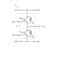
- FIG. 1 is a diagram showing a circuit configuration of a semiconductor module according to an embodiment.
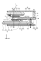
- FIG. 2 is a perspective view of the semiconductor module unit according to the embodiment.
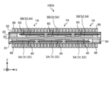
- FIG. 3 is a cross-sectional view of the semiconductor module unit according to the embodiment.
- FIG. 4 is a cross-sectional view showing the structure of a semiconductor module according to the embodiment.
- FIG. 5 is a cross-sectional view of a semiconductor module unit according to a first modified example of the embodiment.
- FIG. 6 is a cross-sectional view of a semiconductor module unit according to a second modification of the embodiment.
- drawings referenced below may show an orthogonal coordinate system that defines the X-axis, Y-axis, and Z-axis directions that are mutually perpendicular, with the positive Z-axis direction being the vertically upward direction.
- Fig. 1 is a diagram showing a circuit configuration of a semiconductor module 1 according to a first embodiment.
- the semiconductor module 1 constitutes part of a power conversion device that converts DC power supplied from a DC power source into AC power.
- the semiconductor module 1 includes a power supply terminal 3, a circuit section 5, and an input/output terminal 7.
- the power supply terminal 3 is a terminal that is connected to a DC power supply (not shown). Specifically, the power supply terminal 3 includes a positive terminal 31 that is connected to the positive side of the DC power supply, and a negative terminal 32 that is connected to the negative side.
- the circuit section 5 includes transistors 51 and 52, which are an example of semiconductor elements, and diodes 53 and 54.
- the two transistors 51 and 52 are connected in series between the positive terminal 31 and the negative terminal 32.
- the diode 53 is connected in anti-parallel to the transistor 51.
- the diode 54 is connected in anti-parallel to the transistor 52.
- Transistors 51 and 52 are, for example, IGBTs (Insulated Gate Bipolar Transistors). Diodes 53 and 54 are reflux diodes for protecting the IGBTs. Transistors 51 and 52 may also be power MOSFETs (Metal Oxide Semiconductor Field Effect Transistors) or GTO (Gate Turn-Off) thyristors.
- IGBTs Insulated Gate Bipolar Transistors
- Diodes 53 and 54 are reflux diodes for protecting the IGBTs.
- Transistors 51 and 52 may also be power MOSFETs (Metal Oxide Semiconductor Field Effect Transistors) or GTO (Gate Turn-Off) thyristors.
- the input/output terminals 7 include a load terminal 71 and a control terminal 72.
- the load terminal 71 is an output terminal for outputting AC power to a load such as a motor.
- the load terminal 71 is connected to the connection node between the two transistors 51 and 52.
- the control terminal 72 is an input terminal to which a drive signal for driving the transistors 51 and 52 is input.
- the semiconductor module 1 configured as described above converts DC power input between the positive terminal 31 and the negative terminal 32 into AC power and outputs it from the load terminal 71 by alternately turning on the two transistors 51, 52 in accordance with a drive signal input from the control terminal 72.
- the semiconductor module 1 configured as described above converts DC power input between the positive terminal 31 and the negative terminal 32 into AC power and outputs it from the load terminal 71 by alternately turning on the two transistors 51, 52 in accordance with a drive signal input from the control terminal 72.
- the semiconductor module 1 needs to dissipate heat generated by the operation of the transistors 51, 52 and the diodes 53, 54.
- the heat sources, the transistors 51, 52 and the diodes 53, 54 are generally thin plates diced from a wafer, with electrodes on both sides and electrically connected by conductors.
- the electrically connected conductor of the semiconductor module 1 is also used as a heat sink and is thermally connected to the substrate.
- the heat transferred to the conductor is dissipated via the insulating substrate.
- the reduction in size leads to high productivity.
- the component area can be made more compact and costs can be reduced, and in the case of molded parts, the productivity can be increased by reducing the mold dimensions and increasing the number of parts that can be produced.
- the semiconductor module 1 When the size of the semiconductor module 1 is reduced, the thermal density inside increases. For this reason, in order to improve the productivity of the semiconductor module 1, it is necessary to improve heat dissipation in addition to reducing the size. Therefore, the semiconductor module 1 according to the embodiment has a structure that can improve heat dissipation while suppressing the occupied area.
- Fig. 2 is a perspective view of the semiconductor module unit 100 according to an embodiment.
- Fig. 3 is a cross-sectional view of the semiconductor module unit 100 according to an embodiment.
- the semiconductor module unit 100 includes three semiconductor modules 1 arranged in a row, and a flow path forming member 20 that houses the three semiconductor modules 1 and forms a flow path for a refrigerant that cools the semiconductor modules 1.
- Each semiconductor module 1 is housed in the flow path forming member 20 with the positive terminal 31, the negative terminal 32, and a portion of the load terminal 71 protruding outside the flow path forming member 20.
- the number of semiconductor modules 1 housed in the flow path forming member 20 may be two or less, or may be four or more.
- the flow path forming member 20 has a coolant inlet section 21 and a coolant outlet section 22.
- the inlet section 21 is provided on the underside of one end of the row of semiconductor modules 1 arranged in a line within the flow path forming member 20.
- the outlet section 22 is provided on the underside of the other end of the row of semiconductor modules 1 arranged in a line within the flow path forming member 20.
- the semiconductor module 1 includes a first substrate 40 and a second substrate 60.
- the first substrate 40 has a first semiconductor element 5A provided on one main surface (here, the top surface).
- the first semiconductor element 5A includes, for example, a transistor 51 and a diode 53.
- the first substrate 40 has a first heat dissipation member 81 provided on the other main surface (here, the bottom surface).
- the first heat dissipation member 81 has heat dissipation pins 86. Note that the first substrate 40 may be provided with heat dissipation fins instead of the heat dissipation pins 86.
- the second substrate 60 is disposed so as to face the first substrate 40.
- the second substrate 60 has a second semiconductor element 5B provided on one of its main surfaces (here, the bottom surface) that faces one of the main surfaces (here, the top surface) of the first substrate 40.
- the second substrate 60 has a second heat dissipation member 82 provided on the other main surface (here, the top surface).
- the second heat dissipation member 82 has heat dissipation pins. Note that the second substrate 60 may be provided with heat dissipation fins instead of the heat dissipation pins 86.
- the flow path forming member 20 can be divided into a lower member 23, a connecting member 24, and an upper member 25.
- the lower member 23 forms a refrigerant flow path with its internal upper surface and the lower surface of the semiconductor module 1.
- the upper member 25 forms a refrigerant flow path with its internal lower surface and the upper surface of the semiconductor module 1.
- the connecting member 24 connects the upper and lower refrigerant flow paths.
- the refrigerant flows into the flow path forming member 20 from the inlet 21, as shown by the white arrow in FIG. 3.
- the refrigerant then passes through the refrigerant flow path formed by the upper surface of the inside of the lower member 23 of the flow path forming member 20 and the lower surface of the semiconductor module 1, and flows out of the flow path forming member 20 from the outlet 22.
- the refrigerant also flows into the flow path forming member 20 from the inlet 21, as shown by the white arrow in FIG. 3.
- the refrigerant then passes through the connecting member 24, passes through the refrigerant flow path formed by the inner lower surface of the upper member 25 of the flow path forming member 20 and the upper surface of the semiconductor module 1, and flows out of the flow path forming member 20 from the outlet 22 via the connecting member 24.
- the semiconductor module 1 is cooled from both the surface of the flow path forming member 20 facing the lower member 23 and the surface of the flow path forming member 20 facing the upper member 25, thereby improving cooling efficiency.
- the semiconductor module 1 is provided with heat dissipation pins 86 on the surface of the flow path forming member 20 facing the lower member 23 and the surface of the flow path forming member 20 facing the lower member 23, the contact area with the refrigerant is increased. This allows the semiconductor module 1 to further improve its cooling efficiency. Note that the semiconductor module 1 can also be provided with heat dissipation fins instead of the heat dissipation pins 86, and the cooling efficiency can be similarly further improved.
- the semiconductor module 1 includes a third heat dissipation member 83 between the first semiconductor element 5A and the second semiconductor element 5B.
- the third heat dissipation member 83 is thermally connected to the first heat dissipation member 81 by a heat conductive member 84.
- the third heat dissipation member 83 is also thermally connected to the second heat dissipation member 82 by a heat conductive member 85.
- the semiconductor module 1 can transfer heat that tends to build up between the first semiconductor element 5A and the second semiconductor element 5B to the first heat dissipation member 81 via the third heat dissipation member 83 and the heat conduction member 84.
- the semiconductor module 1 can transfer heat that tends to build up between the first semiconductor element 5A and the second semiconductor element 5B to the second heat dissipation member 82 via the third heat dissipation member 83 and the heat conduction member 85.
- the heat dissipation efficiency can be improved by the three-layer cooling structure of the first heat dissipation member 81, the second heat dissipation member 82, and the third heat dissipation member 83.
- Fig. 4 is a cross-sectional view showing the structure of the semiconductor module 1 according to the embodiment. Note that Fig. 4 omits the illustration of the flow path forming member 20 and the heat dissipation pins 86 shown in Fig. 3.
- the semiconductor module 1 includes a first substrate 40, a second substrate 60, a first semiconductor element 5A, a second semiconductor element 5B, a first heat dissipation member 81, a second heat dissipation member 82, a third heat dissipation member 83, and a thermal conduction member 84.
- the first substrate 40 includes an insulating substrate 41, a conductive layer 42 bonded to one main surface (here, the upper surface) of the insulating substrate 41, and a conductive layer 43 bonded to the other main surface (here, the lower surface) of the insulating substrate 41.
- the insulating substrate 41 is, for example, a substrate made of ceramics.
- the conductive layers 42, 43 contain, for example, Cu (copper).
- the conductive layers 42, 43 may contain a metal other than Cu.
- the insulating substrate 41 and the conductive layers 42, 43 are bonded, for example, by active metal brazing (AMB) or direct copper bonding (DCB).
- AMB active metal brazing
- DCB direct copper bonding
- the conductive layer 42 which is attached to one of the main surfaces (here, the upper surface) of the insulating substrate 41, is patterned with an electrical circuit.
- the first substrate 40 has a first semiconductor element 5A provided on one of its main surfaces (here, the top surface).
- the thermal conductivity of the first semiconductor element 5A is preferably 100 W/m ⁇ K or more.
- the material of the first semiconductor element 5A is Si (silicon) or SiC (silicon carbide).
- the first semiconductor element 5A includes a transistor 51 and a diode 53.
- the first semiconductor element 5A has a first electrode 55 provided on a main surface opposite to the main surface that abuts the conductive layer 42 of the first substrate 40.
- the first electrode 55 is, for example, a bus bar.
- the first electrode 55 connects a terminal provided on the first semiconductor element 5A to an electrical circuit patterned on the conductive layer 42.
- the first semiconductor element 5A and the members located above and below the first semiconductor element 5A are bonded by a sintered material.
- the sintered material is preferably, for example, Ag (silver) or Cu. This provides the bonded portions between the first semiconductor element 5A and the members located above and below the first semiconductor element 5A with improved heat resistance and heat dissipation, compared to solder.
- the first substrate 40 has a first heat dissipation member 81 provided on the other main surface.
- the first heat dissipation member 81 includes a flat heat dissipation plate 81A and a heat dissipation pin 86 (see FIG. 3).
- the heat dissipation plate 81A and the heat dissipation pin 86 are preferably made of a metal whose main component is, for example, Cu or Al (aluminum).
- the first heat dissipation member 81 has a main surface 81B opposite to the main surface facing the first substrate 40 in the heat dissipation plate 81A, which constitutes part of the inner surface of the refrigerant flow path.
- the heat dissipation pins 86 or heat dissipation fins are provided so as to protrude into the refrigerant flow path from the main surface 81B, which constitutes part of the inner surface of the refrigerant flow path in the heat dissipation plate 81A. Note that the first heat dissipation member 81 does not necessarily have to be provided with the heat dissipation pins 86 or heat dissipation fins.
- the second substrate 60 includes an insulating substrate 61, a conductive layer 62 bonded to one main surface (here, the bottom surface) of the insulating substrate 61, and a conductive layer 63 bonded to the other main surface (here, the top surface) of the insulating substrate 61.
- the insulating substrate 61 is, for example, a substrate made of ceramics.
- the conductive layers 62, 63 contain, for example, Cu.
- the conductive layers 62, 63 may contain a metal other than Cu.
- the insulating substrate 61 and the conductive layers 62, 63 are bonded, for example, by AMB or DCB.
- the conductive layer 62 which is attached to one of the main surfaces (here, the lower surface) of the insulating substrate 61, is patterned with an electrical circuit.
- the second substrate 60 has a second semiconductor element 5B provided on one of its main surfaces (here, the bottom surface).
- the thermal conductivity of the second semiconductor element 5B is preferably 100 W/m ⁇ K or more.
- the material of the second semiconductor element 5B is Si or SiC.
- the second semiconductor element 5B includes a transistor 52 and a diode 54.
- the second semiconductor element 5B has a second electrode 56 provided on a main surface opposite to the main surface that abuts the conductive layer 62 of the second substrate 60.
- the second electrode 56 is, for example, a bus bar.
- the second electrode 56 connects a terminal provided on the second semiconductor element 5B to an electrical circuit patterned on the conductive layer 62.
- the first semiconductor element 5A and the second semiconductor element 5B and the members located above and below the first semiconductor element 5A and the second semiconductor element 5B are bonded with a sintered material. This allows the second semiconductor element 5B and the members located above and below the second semiconductor element 5B to be stacked without gaps, compared to wire bonding.
- the sintered material is preferably, for example, Ag or Cu. This improves the heat resistance and heat dissipation of the joint between the second semiconductor element 5B and the members located above and below the second semiconductor element 5B compared to solder.
- the second substrate 60 has a second heat dissipation member 82 provided on the other main surface.
- the second heat dissipation member 82 includes a flat heat dissipation plate 82A and a heat dissipation pin 86 (see FIG. 3).
- the heat dissipation plate 82A and the heat dissipation pin 86 are preferably made of a metal whose main component is, for example, Cu or Al.
- the second heat dissipation member 82 has a main surface 82B opposite to the main surface of the heat dissipation plate 82A that faces the second substrate 60, which forms part of the inner surface of the refrigerant flow path.
- the heat dissipation pins 86 or heat dissipation fins are provided so as to protrude into the refrigerant flow path from the main surface 82B that forms part of the inner surface of the refrigerant flow path in the heat dissipation plate 82A. Note that the second heat dissipation member 82 does not necessarily have to be provided with the heat dissipation pins 86 or heat dissipation fins.
- the third heat dissipation member 83 is at least partially sandwiched between the first electrode 55 and the second electrode 56. In other words, it is disposed between the first semiconductor element 5A and the second semiconductor element 5B. There are no particular limitations on the thickness of the third heat dissipation member 83, but a thickness of 0.01 to 5 mm is preferable.
- the third heat dissipation member 83 is preferably a metal whose main component is Cu or Al.
- the third heat dissipation member 83 may be a metal other than Cu or Al, or a conductive member.
- the third heat dissipation member 83 may also be a metal spacer, or a structure in which solder is connected to a metal spacer.
- the insulating material may be a high heat resistant resin, an inorganic insulating material, or an insulating material that is a composite of an inorganic insulating material and a resin.
- the thermal conductivity of the insulating material is not particularly limited when the thickness is 0.5 mm or less, but is preferably 1 W/m ⁇ K or more. Inorganic insulating materials are more preferable because they provide high heat resistance and high thermal conductivity. If the surface of the third heat dissipation member 83 is made of Al, an anodized aluminum coating produced by anodizing may be used as the insulating material.
- the third heat dissipation member 83 includes a heat dissipation plate 83A.
- the end surface 83B of the heat dissipation plate 83A in the planar direction of the third heat dissipation member 83 constitutes part of the inner surface of the refrigerant flow path.
- the third heat dissipation member 83 includes a heat dissipation plate 83A including a clamped portion that is clamped by the first electrode 55 and the second electrode 56, and an extension portion that extends from the clamped portion to the connecting member 24 of the flow path forming member 20 (see FIG. 3).
- the third heat dissipation member 83 may form part of the refrigerant flow path by the end face 83B in the planar direction of the heat dissipation plate 83A, in other words, the end face 83B at the tip of the extension portion of the heat dissipation plate 83A, and the inner surface of the connecting member 24.
- the third heat dissipation member 83 is thermally connected to at least one of the first heat dissipation member 81 and the second heat dissipation member 82 by a heat conductive member.
- the heat conduction member 84 thermally connects the third heat dissipation member 83 and the first heat dissipation member 81.
- the heat conduction member 85 thermally connects the third heat dissipation member 83 and the second heat dissipation member 82.
- the heat conduction members 84 and 85 are preferably made of a metal mainly composed of, for example, Cu or Al.
- the heat conduction members 84 and 85 may be joined to the first heat dissipation member 81, the second heat dissipation member 82, and the third heat dissipation member 83 by a joining member such as solder.
- the semiconductor module 1 includes the first heat dissipation member 81, the second heat dissipation member 82, the third heat dissipation member 83, and the thermal conduction members 84 and 85, and therefore the three-layer cooling structure of the first heat dissipation member 81, the second heat dissipation member 82, and the third heat dissipation member 83 can improve heat dissipation efficiency.
- heat generated from the first semiconductor element 5A is transferred to the refrigerant in the refrigerant flow path via paths L1, L2, and L3 indicated by thick arrows in FIG. 4, and path L4 indicated by thick dotted arrow, and is then dissipated.
- the heat generated by the first semiconductor element 5A is transferred to the refrigerant in the refrigerant flow path via path L1 that passes through the third heat dissipation member 83, the second semiconductor element 5B, the second substrate 60, and the second heat dissipation member 82, and is then dissipated.
- the heat generated from the first semiconductor element 5A is transferred to the refrigerant in the refrigerant flow path via path L2, which passes through the first substrate 40 and the first heat dissipation member 81, and dissipated.
- the heat generated from the first semiconductor element 5A is transferred to the refrigerant in the refrigerant flow path via path L3, which passes through the third heat dissipation member 83, the thermal conduction members 84 and 85, the first heat dissipation member 81, and the second heat dissipation member 82, and dissipated.
- the heat generated from the first semiconductor element 5A is transferred to the refrigerant in the refrigerant flow path via the path L4 that transmits the heat from the third heat dissipation member 83 to the connecting member 24, and is dissipated.
- heat generated from the second semiconductor element 5B is transferred to the refrigerant in the refrigerant flow path via paths L1, L2, L3, and L4 and dissipated.
- the three-layer cooling structure of the first heat dissipation member 81, the second heat dissipation member 82, and the third heat dissipation member 83 can improve heat dissipation efficiency.
- the first heat dissipation member 81, the first substrate 40, the first semiconductor element 5A, the third heat dissipation member 83, the second semiconductor element 5B, the second substrate 60, and at least a portion of the second heat dissipation member 82 are stacked in the thickness direction.
- the semiconductor module 1 can reduce the occupied area while improving heat dissipation efficiency compared to when the first heat dissipation member 81, the first substrate 40, the first semiconductor element 5A, the third heat dissipation member 83, the second semiconductor element 5B, the second substrate 60, and the second heat dissipation member 82 are arranged flat.
- the third heat dissipation member 83 is a flat plate, it is preferable for the insulating material of the third heat dissipation member 83 to be in surface contact with the first electrode 55 of the first semiconductor element 5A and the second electrode 56 of the second semiconductor element 5B, as this promotes heat dissipation.
- the first electrode 55 and the second electrode 56 are generally flat, and flat electrodes mainly composed of Cu or Al may be used. Flat electrodes may be provided with bent portions to adjust the height and may be connected to a DBC substrate or the like.
- the third heat dissipation member 83 extends to the portion that is not sandwiched between the first semiconductor element 5A and the second semiconductor element 5B, and is thermally connected to the first heat dissipation member 81, the second heat dissipation member 82, and the refrigerant flow path.
- the bent portions of the first electrode 55 and the second electrode 56 are provided in areas other than the area where the third heat dissipation member 83 contacts.
- the insulating material of the third heat dissipation member 83 may not cover some parts of the heat dissipation plate 83A so that there is no interference between the third heat dissipation member 83 and the sensing terminal extraction portions from the first semiconductor element 5A and the second semiconductor element 5B.
- the third heat dissipation member 83 may also have the necessary thickness to prevent interference between the lead wires of the first semiconductor element 5A and the second semiconductor element 5B, and may also have the role of forming a desired gap between the first semiconductor element 5A and the second semiconductor element 5B.
- extension portion of the third heat dissipation member 83 to the portion not sandwiched between the first semiconductor element 5A and the second semiconductor element 5B may be provided with an extended, non-flat, three-dimensional shape for thermally connecting to the first heat dissipation member 81, the second heat dissipation member 82, and the refrigerant flow path.
- the three-dimensional shape of the extension can be formed by processing the heat dissipation member itself.
- the heat dissipation member can be a flat plate, and a component that can be thermally connected to the first heat dissipation member 81, the second heat dissipation member 82, and the refrigerant flow path can be prepared later.
- the insulating material of the third heat dissipation member 83 may be provided at the locations that contact the first electrodes 55 and second electrodes 56 on the first semiconductor element 5A and the second semiconductor element 5B, but may also be provided on the entire surface of the heat dissipation plate 83A.
- the thermal impact is minor even if it is on the surface where the third heat dissipation member 83 is thermally connected to the first heat dissipation member 81, the second heat dissipation member 82, and the refrigerant flow path.
- Fig. 5 is a cross-sectional view of a semiconductor module unit 100A according to a first modification of the embodiment.
- Fig. 6 is a cross-sectional view of a semiconductor module unit 100B according to a second modification of the embodiment.
- the flow path forming member 20 of the semiconductor module units 100A, 100B shown in Figures 5 and 6 is the same as the flow path forming member shown in Figure 3. For this reason, the flow path forming member is not shown in Figures 5 and 6.
- the heat conduction members 84, 85 connect the end portions in the planar direction of the heat sinks 81A, 82A of the first heat dissipation member 81 and the second heat dissipation member 82 to the end portion in the planar direction of the heat sink 83A of the third heat dissipation member 83.
- thermal conduction members 84, 85 connect the inner portions of the ends of the heat dissipation plates 81A, 82A of the first heat dissipation member 81 and the second heat dissipation member 82 in the planar direction to the inner portions of the ends of the heat dissipation plate 83A of the third heat dissipation member 83 in the planar direction.
- the configuration of the heat conduction members 84, 85 according to the embodiment is not limited to the configuration shown in FIG. 3.
- the heat conduction members 84, 85 may connect the heat dissipation plates 81A, 82A of the first heat dissipation member 81 and the second heat dissipation member 82 to the heat dissipation plate 83A of the third heat dissipation member 83 only at their ends in the planar direction.
- the heat conduction members 84, 85 that connect the portions of the heat dissipation plates 81A, 82A of the first heat dissipation member 81 and the second heat dissipation member 82 that are inward from the ends in the planar direction and the heat dissipation plate 83A of the third heat dissipation member 83 that are inward from the ends in the planar direction may be omitted. Also, either one of the heat conduction members 84, 85 shown in FIG. 5 may be omitted.
- the semiconductor module 1A can achieve a three-layer cooling structure while reducing the material costs of the heat conduction members 84 and 85, thereby improving cooling efficiency compared to a semiconductor module that does not have the third heat dissipation member 83 and the heat conduction members 84 and 85.
- the semiconductor module 1B may be configured by omitting the heat dissipation pins 86 from the semiconductor module 1 shown in FIG. 3. This allows the semiconductor module 1B to reduce the material cost of the heat dissipation pins 86, and thus realizes a three-layer cooling structure while keeping costs down, thereby improving cooling efficiency compared to a semiconductor module that does not include the third heat dissipation member 83 and the thermal conduction members 84, 85.
- first heat dissipation member 81 the second heat dissipation member 82, the third heat dissipation member 83, the heat conduction members 84 and 85, and the heat dissipation pins 86 described in this embodiment can be combined in any manner.
- the heat dissipation pin 86 may not be provided, may be provided on both the first heat dissipation member 81 and the second heat dissipation member 82, or may be provided on at least one of the first heat dissipation member 81 and the second heat dissipation member 82.
- heat conduction members 84 and 85 do not have to be provided, or only one of them may be provided, as long as at least the end in the planar direction of the third heat dissipation member 83 is thermally connected to the connecting member 24 of the flow path forming member 20.
- the present technology can be configured as follows. (1) a first substrate having a first semiconductor element provided on one main surface and a first heat dissipation member provided on the other main surface; a second substrate disposed opposite to the first substrate, the second substrate having a second semiconductor element provided on one main surface facing the one main surface of the first substrate and a second heat dissipation member provided on the other main surface; a third heat dissipation member at least a portion of which is sandwiched between a first electrode provided on a main surface of the first semiconductor element facing the second semiconductor element and a second electrode provided on a main surface of the second semiconductor element facing the first semiconductor element; Semiconductor module.
- the third heat dissipation member is At least a surface of a portion sandwiched between the first electrode and the second electrode is covered with an insulating material.
- the first heat dissipation member is a flat heat sink, the main surface of the heat sink opposite to the main surface facing the first substrate forming a part of an inner surface of the coolant flow path;
- the first heat dissipation member is a heat dissipation pin or a heat dissipation fin protruding from a main surface of the heat dissipation plate that constitutes a part of the inner surface of the refrigerant flow path toward the inside of the refrigerant flow path;
- the second heat dissipation member is a flat heat sink, the main surface of the heat sink opposite to the main surface facing the second substrate forming a part of an inner surface of the coolant flow path; A semiconductor module according to any one of (1) to (4).
- the second heat dissipation member is a heat dissipation pin or a heat dissipation fin protruding from a main surface of the heat dissipation plate that constitutes a part of the inner surface of the refrigerant flow path toward the inside of the refrigerant flow path; A semiconductor module according to (5).
- the third heat dissipation member is A flat heat sink is provided, and an end surface of the heat sink in a planar direction constitutes a part of an inner surface of the refrigerant flow path.
- the first heat dissipation member, the second heat dissipation member, and the third heat dissipation member are A flat heat sink is included.
- the thermal conductive member is an end portion of at least one of the first heat dissipation member and the second heat dissipation member in a surface direction of the heat dissipation plate is connected to an end portion of the third heat dissipation member in a surface direction of the heat dissipation plate;
- the thermal conductive member is a portion of at least one of the first heat dissipation member and the second heat dissipation member that is located inward from an end portion in a surface direction of the heat dissipation plate and a portion of the third heat dissipation member that is located inward from an end portion in a surface direction of the heat dissipation plate;
- At least a portion of the first heat dissipation member, the first substrate, the first semiconductor element, the third heat dissipation member, the second semiconductor element, the second substrate, and the second heat dissipation member are stacked in a thickness direction.
- (12) The first semiconductor element and the second semiconductor element are joined to members located above and below the first semiconductor element and the second semiconductor element by a sintered material.
- a semiconductor module according to any one of (1) to (11). (13) The sintered material is silver or copper;
Landscapes
- Engineering & Computer Science (AREA)
- Microelectronics & Electronic Packaging (AREA)
- Physics & Mathematics (AREA)
- Thermal Sciences (AREA)
- Cooling Or The Like Of Semiconductors Or Solid State Devices (AREA)
Abstract
Description
まず、実施形態に係る半導体モジュールの回路構成について図1を参照して説明する。図1は、第1実施形態に係る半導体モジュール1の回路構成を示す図である。
まず、実施形態に係る半導体モジュールユニット100の構成について、図1および図2を参照して説明する。図2は、実施形態に係る半導体モジュールユニット100の透視斜視図である。図3は、実施形態に係る半導体モジュールユニット100の断面図である。
次に、実施形態に係る半導体モジュール1の構造について、図4を参照して説明する。図4は、実施形態に係る半導体モジュール1の構造を示す断面図である。なお、図4では、図3に示す流路形成部材20および放熱ピン86の図示が省略されている。
次に、実施形態の変形例に係る半導体モジュールユニット100A,100Bの構成について、図5および図6を参照して説明図する。図5は、実施形態の第1変形例に係る半導体モジュールユニット100Aの断面図である。図6は、実施形態の第2変形例に係る半導体モジュールユニット100Bの断面図である。
(1)
一方の主面に第1の半導体素子が設けられ、他方の主面に第1放熱部材が設けられる第1基板と、
前記第1基板に対して対向するように配置され、前記第1基板の前記一方の主面に面する一方の主面に第2の半導体素子が設けられ、他方の主面に第2放熱部材が設けられる第2基板と、
前記第1の半導体素子における前記第2の半導体素子に面する側の主面に設けられる第1電極と、前記第2の半導体素子における前記第1の半導体素子に面する側の主面に設けられる第2電極とによって、少なくとも一部が挟持される第3放熱部材と、を備える、
半導体モジュール。
(2)
前記第3放熱部材は、
少なくとも前記第1電極および前記第2電極によって挟持される部分の表面が絶縁材によって被覆される、
(1)に記載の半導体モジュール。
(3)
前記第1放熱部材は、
平板状の放熱板を含み、前記放熱板における前記第1基板に面する側の主面とは反対側の主面が冷媒流路の内側面の一部を構成する、
(1)または(2)に記載の半導体モジュール。
(4)
前記第1放熱部材は、
前記放熱板における前記冷媒流路の内側面の一部を構成する主面から前記冷媒流路内へ向けて突出する放熱ピンまたは放熱フィンを備える、
(3)に記載の半導体モジュール。
(5)
前記第2放熱部材は、
平板状の放熱板を含み、前記放熱板における前記第2基板に面する側の主面とは反対側の主面が冷媒流路の内側面の一部を構成する、
(1)から(4)のいずれか一つに記載の半導体モジュール。
(6)
前記第2放熱部材は、
前記放熱板における前記冷媒流路の内側面の一部を構成する主面から前記冷媒流路内へ向けて突出する放熱ピンまたは放熱フィンを備える、
(5)に記載の半導体モジュール。
(7)
前記第3放熱部材は、
平板状の放熱板を含み、前記放熱板における面方向の端面が冷媒流路の内側面の一部を構成する、
(1)から(6)のいずれか一つに記載の半導体モジュール。
(8)
前記第1放熱部材および前記第2放熱部材のうち少なくともいずれか一方と前記第3放熱部材とを接続する熱伝導部材、を備える、
(1)から(7)のいずれか一つに記載の半導体モジュール。
(9)
前記第1放熱部材、前記第2放熱部材、および、前記第3放熱部材は、
平板状の放熱板を含み、
前記熱伝導部材は、
前記第1放熱部材および前記第2放熱部材のうち少なくともいずれか一方の前記放熱板の面方向における端部と、前記第3放熱部材の前記放熱板の面方向における端部とを接続する、
(8)に記載の半導体モジュール。
(10)
前記熱伝導部材は、
前記第1放熱部材および前記第2放熱部材のうち少なくともいずれか一方の前記放熱板の面方向における端部よりも内側の部分と、前記第3放熱部材の前記放熱板の面方向における端部よりも内側の部分とを接続する、
(9)に記載の半導体モジュール。
(11)
前記第1放熱部材、前記第1基板、前記第1の半導体素子、前記第3放熱部材、前記第2の半導体素子、前記第2基板、および、前記第2放熱部材の少なくとも一部が、厚さ方向に積層される、
(1)から(10)のいずれか一つに記載の半導体モジュール。
(12)
前記第1の半導体素子および前記第2の半導体素子と、前記第1の半導体素子および前記第2の半導体素子の上下に位置する部材とが、焼結材によって接合される、
(1)から(11)のいずれか一つに記載の半導体モジュール。
(13)
前記焼結材は、銀または銅である、
(12)に記載の半導体モジュール。
(14)
一列に配置される複数個の(1)から(13)のいずれか一つに記載の半導体モジュールと、
複数個の前記半導体モジュールを収納し、複数個の前記半導体モジュールを冷却する冷媒の流路を形成する流路形成部材とを含む、半導体モジュールユニット。
20 流路形成部材
21 流入部
22 流出部
23 下部材
24 連結部材
25 上部材
3 電源端子
31 正極端子
32 負極端子
40 第1基板
41 絶縁基板
42,43 導電層
5 回路部
5A 第1の半導体素子
5B 第2の半導体素子
51,52 トランジスタ
53,54 ダイオード
55 第1電極
56 第2電極
60 第2基板
61 絶縁基板
62,63 導電層
7 入出力端子
71 負荷端子
72 制御端子
81 第1放熱部材
81A 放熱板
81B 主面
82 第2放熱部材
82A 放熱板
82B 主面
83 第3放熱部材
83A 放熱板
83B 端面
83C 絶縁材
84,85 熱伝導部材
86 放熱ピン
100,100A,100B 半導体モジュールユニット
L1,L2,L3,L4 経路
Claims (14)
- 一方の主面に第1の半導体素子が設けられ、他方の主面に第1放熱部材が設けられる第1基板と、
前記第1基板に対して対向するように配置され、前記第1基板の前記一方の主面に面する一方の主面に第2の半導体素子が設けられ、他方の主面に第2放熱部材が設けられる第2基板と、
前記第1の半導体素子における前記第2の半導体素子に面する側の主面に設けられる第1電極と、前記第2の半導体素子における前記第1の半導体素子に面する側の主面に設けられる第2電極とによって、少なくとも一部が挟持される第3放熱部材と、を備える、
半導体モジュール。 - 前記第3放熱部材は、
少なくとも前記第1電極および前記第2電極によって挟持される部分の表面が絶縁材によって被覆される、
請求項1に記載の半導体モジュール。 - 前記第1放熱部材は、
平板状の放熱板を含み、前記放熱板における前記第1基板に面する側の主面とは反対側の主面が冷媒流路の内側面の一部を構成する、
請求項1または請求項2に記載の半導体モジュール。 - 前記第1放熱部材は、
前記放熱板における前記冷媒流路の内側面の一部を構成する主面から前記冷媒流路内へ向けて突出する放熱ピンまたは放熱フィンを備える、
請求項3に記載の半導体モジュール。 - 前記第2放熱部材は、
平板状の放熱板を含み、前記放熱板における前記第2基板に面する側の主面とは反対側の主面が冷媒流路の内側面の一部を構成する、
請求項1または請求項2に記載の半導体モジュール。 - 前記第2放熱部材は、
前記放熱板における前記冷媒流路の内側面の一部を構成する主面から前記冷媒流路内へ向けて突出する放熱ピンまたは放熱フィンを備える、
請求項5に記載の半導体モジュール。 - 前記第3放熱部材は、
平板状の放熱板を含み、前記放熱板における面方向の端面が冷媒流路の内側面の一部を構成する、
請求項1または請求項2に記載の半導体モジュール。 - 前記第1放熱部材および前記第2放熱部材のうち少なくともいずれか一方と前記第3放熱部材とを接続する熱伝導部材、を備える、
請求項1または請求項2に記載の半導体モジュール。 - 前記第1放熱部材、前記第2放熱部材、および、前記第3放熱部材は、
平板状の放熱板を含み、
前記熱伝導部材は、
前記第1放熱部材および前記第2放熱部材のうち少なくともいずれか一方の前記放熱板の面方向における端部と、前記第3放熱部材の前記放熱板の面方向における端部とを接続する、
請求項8に記載の半導体モジュール。 - 前記熱伝導部材は、
前記第1放熱部材および前記第2放熱部材のうち少なくともいずれか一方の前記放熱板の面方向における端部よりも内側の部分と、前記第3放熱部材の前記放熱板の面方向における端部よりも内側の部分とを接続する、
請求項9に記載の半導体モジュール。 - 前記第1放熱部材、前記第1基板、前記第1の半導体素子、前記第3放熱部材、前記第2の半導体素子、前記第2基板、および、前記第2放熱部材の少なくとも一部が、厚さ方向に積層される、
請求項1または請求項2に記載の半導体モジュール。 - 前記第1の半導体素子および前記第2の半導体素子と、前記第1の半導体素子および前記第2の半導体素子の上下に位置する部材とが、焼結材によって接合される、
請求項1または請求項2に記載の半導体モジュール。 - 前記焼結材は、銀または銅である、
請求項12に記載の半導体モジュール。 - 一列に配置される複数個の請求項1または請求項2に記載の半導体モジュールと、
複数個の前記半導体モジュールを収納し、複数個の前記半導体モジュールを冷却する冷媒の流路を形成する流路形成部材とを含む、半導体モジュールユニット。
Priority Applications (3)
| Application Number | Priority Date | Filing Date | Title |
|---|---|---|---|
| DE112023003209.2T DE112023003209T5 (de) | 2022-09-30 | 2023-09-21 | Halbleitermodul und Halbleitermoduleinheit |
| CN202380068474.7A CN119948623A (zh) | 2022-09-30 | 2023-09-21 | 半导体模块及半导体模块单元 |
| JP2024549280A JPWO2024070883A1 (ja) | 2022-09-30 | 2023-09-21 |
Applications Claiming Priority (2)
| Application Number | Priority Date | Filing Date | Title |
|---|---|---|---|
| JP2022-158798 | 2022-09-30 | ||
| JP2022158798 | 2022-09-30 |
Publications (1)
| Publication Number | Publication Date |
|---|---|
| WO2024070883A1 true WO2024070883A1 (ja) | 2024-04-04 |
Family
ID=90477609
Family Applications (1)
| Application Number | Title | Priority Date | Filing Date |
|---|---|---|---|
| PCT/JP2023/034253 Ceased WO2024070883A1 (ja) | 2022-09-30 | 2023-09-21 | 半導体モジュールおよび半導体モジュールユニット |
Country Status (4)
| Country | Link |
|---|---|
| JP (1) | JPWO2024070883A1 (ja) |
| CN (1) | CN119948623A (ja) |
| DE (1) | DE112023003209T5 (ja) |
| WO (1) | WO2024070883A1 (ja) |
Citations (5)
| Publication number | Priority date | Publication date | Assignee | Title |
|---|---|---|---|---|
| JP2005123233A (ja) * | 2003-10-14 | 2005-05-12 | Denso Corp | 半導体装置の冷却構造 |
| WO2009150875A1 (ja) * | 2008-06-12 | 2009-12-17 | 株式会社安川電機 | パワーモジュールおよびその制御方法 |
| WO2011064841A1 (ja) * | 2009-11-25 | 2011-06-03 | トヨタ自動車株式会社 | 半導体装置の冷却構造 |
| JP2019021864A (ja) * | 2017-07-21 | 2019-02-07 | 国立研究開発法人産業技術総合研究所 | パワーモジュール |
| JP2019186390A (ja) * | 2018-04-11 | 2019-10-24 | 日産自動車株式会社 | 半導体装置および電力変換装置 |
-
2023
- 2023-09-21 JP JP2024549280A patent/JPWO2024070883A1/ja active Pending
- 2023-09-21 WO PCT/JP2023/034253 patent/WO2024070883A1/ja not_active Ceased
- 2023-09-21 DE DE112023003209.2T patent/DE112023003209T5/de active Pending
- 2023-09-21 CN CN202380068474.7A patent/CN119948623A/zh active Pending
Patent Citations (5)
| Publication number | Priority date | Publication date | Assignee | Title |
|---|---|---|---|---|
| JP2005123233A (ja) * | 2003-10-14 | 2005-05-12 | Denso Corp | 半導体装置の冷却構造 |
| WO2009150875A1 (ja) * | 2008-06-12 | 2009-12-17 | 株式会社安川電機 | パワーモジュールおよびその制御方法 |
| WO2011064841A1 (ja) * | 2009-11-25 | 2011-06-03 | トヨタ自動車株式会社 | 半導体装置の冷却構造 |
| JP2019021864A (ja) * | 2017-07-21 | 2019-02-07 | 国立研究開発法人産業技術総合研究所 | パワーモジュール |
| JP2019186390A (ja) * | 2018-04-11 | 2019-10-24 | 日産自動車株式会社 | 半導体装置および電力変換装置 |
Also Published As
| Publication number | Publication date |
|---|---|
| DE112023003209T5 (de) | 2025-05-15 |
| JPWO2024070883A1 (ja) | 2024-04-04 |
| CN119948623A (zh) | 2025-05-06 |
Similar Documents
| Publication | Publication Date | Title |
|---|---|---|
| JP7428018B2 (ja) | 半導体モジュール | |
| JP7428017B2 (ja) | 半導体モジュール | |
| JP5627499B2 (ja) | 半導体モジュールを備えた半導体装置 | |
| CN107112294B (zh) | 半导体装置以及功率模块 | |
| JP4192396B2 (ja) | 半導体スイッチングモジュ−ル及びそれを用いた半導体装置 | |
| JP6786416B2 (ja) | 半導体装置 | |
| CN108735692B (zh) | 半导体装置 | |
| JP7532813B2 (ja) | 半導体モジュール | |
| JP7060104B2 (ja) | 半導体装置 | |
| JP2022179649A (ja) | 半導体装置及びその製造方法 | |
| JP7491043B2 (ja) | 半導体モジュール | |
| JP7183594B2 (ja) | 半導体装置 | |
| JP7567191B2 (ja) | 半導体モジュール | |
| WO2013172291A1 (ja) | パワーモジュール半導体装置 | |
| WO2009150875A1 (ja) | パワーモジュールおよびその制御方法 | |
| CN109390300B (zh) | 半导体装置 | |
| US20240096730A1 (en) | Semiconductor Module Having Double Sided Heat Dissipation Structure and Method for Fabricating the Same | |
| US20030090915A1 (en) | Inverter apparatus and method of manufacturing the same | |
| JP7428019B2 (ja) | 半導体モジュール | |
| WO2022059251A1 (ja) | 半導体装置 | |
| CN111524877B (zh) | 一种双面散热功率模块 | |
| JP7163583B2 (ja) | 半導体装置 | |
| CN113748509A (zh) | 半导体装置 | |
| JP2023134143A (ja) | 半導体モジュール、半導体装置、及び車両 | |
| JP5402778B2 (ja) | 半導体モジュールを備えた半導体装置 |
Legal Events
| Date | Code | Title | Description |
|---|---|---|---|
| 121 | Ep: the epo has been informed by wipo that ep was designated in this application |
Ref document number: 23872109 Country of ref document: EP Kind code of ref document: A1 |
|
| WWE | Wipo information: entry into national phase |
Ref document number: 2024549280 Country of ref document: JP |
|
| WWE | Wipo information: entry into national phase |
Ref document number: 112023003209 Country of ref document: DE Ref document number: 202380068474.7 Country of ref document: CN |
|
| WWP | Wipo information: published in national office |
Ref document number: 202380068474.7 Country of ref document: CN |
|
| WWP | Wipo information: published in national office |
Ref document number: 112023003209 Country of ref document: DE |
|
| 122 | Ep: pct application non-entry in european phase |
Ref document number: 23872109 Country of ref document: EP Kind code of ref document: A1 |