WO2024070848A1 - プラズマ処理装置 - Google Patents
プラズマ処理装置 Download PDFInfo
- Publication number
- WO2024070848A1 WO2024070848A1 PCT/JP2023/034100 JP2023034100W WO2024070848A1 WO 2024070848 A1 WO2024070848 A1 WO 2024070848A1 JP 2023034100 W JP2023034100 W JP 2023034100W WO 2024070848 A1 WO2024070848 A1 WO 2024070848A1
- Authority
- WO
- WIPO (PCT)
- Prior art keywords
- power
- unit
- plasma processing
- processing apparatus
- coil
- Prior art date
- Legal status (The legal status is an assumption and is not a legal conclusion. Google has not performed a legal analysis and makes no representation as to the accuracy of the status listed.)
- Ceased
Links
Images


Classifications
-
- H—ELECTRICITY
- H01—ELECTRIC ELEMENTS
- H01J—ELECTRIC DISCHARGE TUBES OR DISCHARGE LAMPS
- H01J37/00—Discharge tubes with provision for introducing objects or material to be exposed to the discharge, e.g. for the purpose of examination or processing thereof
- H01J37/32—Gas-filled discharge tubes
- H01J37/32009—Arrangements for generation of plasma specially adapted for examination or treatment of objects, e.g. plasma sources
- H01J37/32082—Radio frequency generated discharge
- H01J37/32174—Circuits specially adapted for controlling the RF discharge
- H01J37/32183—Matching circuits
-
- H—ELECTRICITY
- H01—ELECTRIC ELEMENTS
- H01J—ELECTRIC DISCHARGE TUBES OR DISCHARGE LAMPS
- H01J37/00—Discharge tubes with provision for introducing objects or material to be exposed to the discharge, e.g. for the purpose of examination or processing thereof
- H01J37/32—Gas-filled discharge tubes
- H01J37/32009—Arrangements for generation of plasma specially adapted for examination or treatment of objects, e.g. plasma sources
- H01J37/32082—Radio frequency generated discharge
- H01J37/321—Radio frequency generated discharge the radio frequency energy being inductively coupled to the plasma
- H01J37/3211—Antennas, e.g. particular shapes of coils
-
- H—ELECTRICITY
- H01—ELECTRIC ELEMENTS
- H01J—ELECTRIC DISCHARGE TUBES OR DISCHARGE LAMPS
- H01J37/00—Discharge tubes with provision for introducing objects or material to be exposed to the discharge, e.g. for the purpose of examination or processing thereof
- H01J37/32—Gas-filled discharge tubes
- H01J37/32009—Arrangements for generation of plasma specially adapted for examination or treatment of objects, e.g. plasma sources
- H01J37/32082—Radio frequency generated discharge
- H01J37/32174—Circuits specially adapted for controlling the RF discharge
-
- H—ELECTRICITY
- H02—GENERATION; CONVERSION OR DISTRIBUTION OF ELECTRIC POWER
- H02J—ELECTRIC POWER NETWORKS; CIRCUIT ARRANGEMENTS OR SYSTEMS FOR SUPPLYING OR DISTRIBUTING ELECTRIC POWER; SYSTEMS FOR STORING ELECTRIC ENERGY
- H02J50/00—Circuit arrangements or systems for wireless supply or distribution of electric power
- H02J50/10—Circuit arrangements or systems for wireless supply or distribution of electric power using inductive coupling
- H02J50/12—Circuit arrangements or systems for wireless supply or distribution of electric power using inductive coupling of the resonant type
-
- H—ELECTRICITY
- H02—GENERATION; CONVERSION OR DISTRIBUTION OF ELECTRIC POWER
- H02J—ELECTRIC POWER NETWORKS; CIRCUIT ARRANGEMENTS OR SYSTEMS FOR SUPPLYING OR DISTRIBUTING ELECTRIC POWER; SYSTEMS FOR STORING ELECTRIC ENERGY
- H02J7/00—Circuit arrangements for charging or discharging batteries or for supplying loads from batteries
- H02J7/90—Regulation of charging or discharging current or voltage
-
- H—ELECTRICITY
- H05—ELECTRIC TECHNIQUES NOT OTHERWISE PROVIDED FOR
- H05H—PLASMA TECHNIQUE; PRODUCTION OF ACCELERATED ELECTRICALLY-CHARGED PARTICLES OR OF NEUTRONS; PRODUCTION OR ACCELERATION OF NEUTRAL MOLECULAR OR ATOMIC BEAMS
- H05H1/00—Generating plasma; Handling plasma
- H05H1/24—Generating plasma
- H05H1/46—Generating plasma using applied electromagnetic fields, e.g. high frequency or microwave energy
Definitions
- An exemplary embodiment of the present disclosure relates to a plasma processing apparatus.
- a plasma processing apparatus is used in plasma processing.
- the plasma processing apparatus includes a chamber and a substrate support (mounting table) disposed within the chamber.
- the substrate support has a base (lower electrode) and an electrostatic chuck for holding the substrate.
- a temperature adjustment element e.g., a heater
- a filter is provided between the temperature adjustment element and the power supply for the temperature adjustment element to attenuate or block high-frequency noise that enters lines such as power supply lines and/or signal lines from the high-frequency electrodes and/or other electrical components in the chamber.
- Patent Document 1 One type of such plasma processing apparatus is described in Patent Document 1 listed below.
- An exemplary embodiment of the present disclosure provides a technology for supplying power through electromagnetic induction coupling without going through a power storage unit in accordance with the load resistance value of a power consuming component in a plasma processing apparatus.
- a plasma processing apparatus in one exemplary embodiment, includes a plasma processing chamber, a substrate support, an electrode or antenna, a high frequency power source, at least one power consuming member, a receiving coil, a transmitting coil, a power transmitting unit, and a control unit.
- the substrate support is disposed in the plasma processing chamber.
- the electrode or antenna is disposed outside with respect to a plasma processing space in the plasma processing chamber.
- the space in the plasma processing chamber is located between the electrode or antenna and the substrate support.
- the high frequency power source is configured to generate high frequency power and is electrically connected to the substrate support, the electrode or antenna.
- At least one power consuming member is disposed in the plasma processing chamber or in the substrate support.
- the receiving coil is electrically connected to the at least one power consuming member.
- the transmitting coil is electromagnetically inductively coupled to the receiving coil.
- the transmitting unit is electrically connected to the transmitting coil to supply power to the transmitting coil.
- the transmitting unit includes a voltage detector configured to detect an input voltage to the transmitting coil and a current detector configured to detect an input current to the transmitting coil.
- the control unit is configured to determine a required power level according to parameter values including an input impedance calculated from an input voltage and an input current or a load resistance value of at least one power consuming component, and to control the power transmission unit to output output power having the required power level.
- a technology that supplies power by electromagnetic induction coupling without going through a power storage unit according to the load resistance value of a power consuming component in a plasma processing apparatus.
- FIG. 1 is a diagram for explaining a configuration example of a plasma processing system.
- FIG. 1 is a diagram for explaining a configuration example of a capacitively coupled plasma processing apparatus.
- 1 is a schematic diagram of a plasma processing apparatus according to an exemplary embodiment
- FIG. 13 is a schematic diagram of a plasma processing apparatus according to another exemplary embodiment.
- FIG. 13 is a schematic diagram of a plasma processing apparatus according to yet another exemplary embodiment.
- FIG. 13 is a schematic diagram of a plasma processing apparatus according to yet another exemplary embodiment.
- FIG. 13 is a schematic diagram of a plasma processing apparatus according to yet another exemplary embodiment.
- FIG. 2 illustrates a power transmission unit according to an exemplary embodiment.
- FIG. 1 is a diagram for explaining a configuration example of a plasma processing system.
- FIG. 1 is a diagram for explaining a configuration example of a capacitively coupled plasma processing apparatus.
- 1 is a schematic diagram of a plasma processing apparatus according to an exemplary embodiment
- FIG. 13 is
- FIG. 2 illustrates a power transmitting coil section and a power receiving coil section according to an exemplary embodiment.
- FIG. 2 illustrates a power transmitting coil section and a power receiving coil section according to an exemplary embodiment.
- FIG. 2 illustrates a power transmitting coil section and a power receiving coil section according to an exemplary embodiment.
- 11 is a graph illustrating impedance characteristics of a receiving coil section according to an exemplary embodiment.
- FIG. 2 illustrates an RF filter according to an exemplary embodiment.
- FIG. 2 illustrates a rectifying and smoothing unit according to an exemplary embodiment.
- FIG. 2 illustrates an RF filter according to an exemplary embodiment.
- FIG. 2 is a diagram illustrating a communication unit of a power transmitting unit and a communication unit of a rectifying and smoothing unit according to an exemplary embodiment.
- FIG. 13 is a schematic diagram of a plasma processing apparatus according to yet another exemplary embodiment.
- FIG. 13 is a schematic diagram of a plasma processing apparatus according to yet another exemplary embodiment.
- FIG. 13 is a diagram illustrating a communication unit of a power transmitting unit and a communication unit of a rectifying and smoothing unit according to another exemplary embodiment.
- FIG. 13 is a schematic diagram of a plasma processing apparatus according to yet another exemplary embodiment.
- FIG. 13 is a schematic diagram of a plasma processing apparatus according to yet another exemplary embodiment.
- FIG. 13 is a schematic diagram of a plasma processing apparatus according to yet another exemplary embodiment.
- FIG. 1 illustrates a voltage controlled converter according to an exemplary embodiment.
- FIG. 2 illustrates a constant voltage controller according to an exemplary embodiment.
- FIG. 13 illustrates a constant voltage controller according to another exemplary embodiment.
- FIG. 13 is a schematic diagram of a plasma processing apparatus according to yet another exemplary embodiment.
- 4 is a diagram showing an example of an equivalent circuit of a power transmitting coil section and a power receiving coil section;
- FIG. 13 is a diagram showing an example of at least one table.
- FIG. 13 is a diagram showing an example of at least one table.
- FIG. 13 is a schematic diagram of a plasma processing apparatus according to yet another exemplary embodiment.
- FIG. 4 is a timing chart showing an example of a load resistance value, an input impedance, a transmission power, and a state of a switching element.
- 4 is a flow diagram of a power supply method according to an exemplary embodiment.
- 4 is a flow diagram of a power supply method according to an exemplary embodiment.
- FIG. 13 is a schematic diagram of a plasma processing apparatus according to yet another exemplary embodiment.
- FIG. 13 is a schematic diagram of a plasma processing apparatus according to yet another exemplary embodiment.
- FIG. 13 is a schematic diagram of a plasma processing apparatus according to yet another exemplary embodiment.
- FIG. 13 is a schematic diagram of a plasma processing apparatus according to yet another exemplary embodiment.
- FIG. 13 is a diagram showing a power transmitting coil section and a power receiving coil section in a plasma processing apparatus according to yet another exemplary embodiment.
- FIG. 13 is a diagram showing a power transmitting coil section and a power receiving coil section in a plasma processing apparatus according to yet another exemplary embodiment.
- FIG. 13 is a schematic diagram of a plasma processing apparatus according to yet another exemplary embodiment.
- FIG. 13 is a schematic diagram of a plasma processing apparatus according to yet another exemplary embodiment.
- FIG. 13 illustrates an immittance converter in a plasma processing apparatus according to yet another exemplary embodiment.
- FIG. 1 illustrates a power transmitter that may be employed in a plasma processing apparatus according to various exemplary embodiments.
- FIG. 1 illustrates a power transmitter and an AC/DC converter that may be employed in a plasma processing apparatus according to various exemplary embodiments.
- FIG. 1 illustrates a power transmitter and an AC/DC converter that may be employed in a plasma processing apparatus according to various exemplary embodiments.
- 1A-1C are diagrams illustrating a receiving coil section that may be employed in a plasma processing apparatus according to various exemplary embodiments.
- 1A and 1B are diagrams illustrating configurations of a receiving coil and a transmitting coil that may be employed in a plasma processing apparatus according to various exemplary embodiments.
- 1A and 1B are diagrams illustrating configurations of a receiving coil and a transmitting coil that may be employed in a plasma processing apparatus according to various exemplary embodiments.
- FIG. 1A to 1C are diagrams showing configurations of a receiving coil section and a rectification/smoothing section that can be employed in plasma processing apparatuses according to various exemplary embodiments.
- 1A to 1C are diagrams illustrating configurations of a power receiving coil section and a rectification/smoothing section that can be employed in a plasma processing apparatus according to various exemplary embodiments.
- FIG. 1 illustrates an integrated power supply configuration that may be employed in a plasma processing apparatus according to various exemplary embodiments.
- FIG. 1 illustrates an integrated power supply configuration that may be employed in a plasma processing apparatus according to various exemplary embodiments.
- FIG. 1 illustrates an integrated power supply configuration that may be employed in a plasma processing apparatus according to various exemplary embodiments.
- FIG. 1 illustrates an integrated power supply configuration that may be employed in a plasma processing apparatus according to various exemplary embodiments.
- FIG. 1 illustrates an integrated power supply configuration that may be employed in a plasma processing apparatus according to various exemplary embodiments.
- FIG. 1 illustrates an integrated power supply configuration that may be employed in a plasma processing apparatus according to various exemplary embodiments.
- FIG. 1 illustrates an integrated power supply configuration that may be employed in a plasma processing apparatus according to various exemplary embodiments.
- FIG. 1 illustrates an integrated power supply configuration that may be employed in a plasma processing apparatus according to various exemplary embodiments.
- FIG. 1 illustrates an integrated power supply configuration that may be employed in a plasma processing apparatus according to various exemplary embodiments.
- FIG. 1 illustrates an integrated power supply configuration that may be employed in a plasma processing apparatus according to various exemplary embodiments.
- FIG. 1 illustrates an integrated power supply configuration that may be employed in a plasma processing apparatus according to various exemplary embodiments.
- FIG. 1 illustrates an integrated power supply configuration that may be employed in a plasma processing apparatus according to various exemplary embodiments.
- FIG. 1 illustrates an integrated power supply configuration that may be employed in a plasma processing apparatus according to various exemplary embodiments.
- FIG. 1 illustrates an integrated power supply configuration that may be employed in a plasma processing apparatus according to various exemplary embodiments.
- FIG. 1 illustrates an integrated power supply configuration that may be employed in a plasma processing apparatus according to various exemplary embodiments.
- FIG. 1 illustrates an integrated power supply configuration that may be employed in a plasma processing apparatus according to various exemplary embodiments.
- FIG. 1 illustrates an integrated power supply configuration that may be employed in a plasma processing apparatus according to various exemplary embodiments.
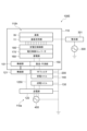
- FIG. 1 is a diagram for explaining an example of the configuration of a plasma processing system.
- the plasma processing system includes a plasma processing device 1 and a control unit 2.
- the plasma processing system is an example of a substrate processing system
- the plasma processing device 1 is an example of a substrate processing device.
- the plasma processing device 1 includes a plasma processing chamber 10, a substrate support unit 11, and a plasma generation unit 12.
- the plasma processing chamber 10 has a plasma processing space.
- the plasma processing chamber 10 also has at least one gas supply port for supplying at least one processing gas to the plasma processing space, and at least one gas exhaust port for exhausting gas from the plasma processing space.
- the gas supply port is connected to a gas supply unit 20 described later, and the gas exhaust port is connected to an exhaust system 40 described later.
- the substrate support unit 11 is disposed in the plasma processing space, and has a substrate support surface for supporting a substrate.
- the plasma generating unit 12 is configured to generate plasma from at least one processing gas supplied into the plasma processing space.
- the plasma formed in the plasma processing space may be capacitively coupled plasma (CCP), inductively coupled plasma (ICP), ECR plasma (Electron-Cyclotron-Resonance Plasma), Helicon Wave Plasma (HWP), or Surface Wave Plasma (SWP), etc.
- various types of plasma generating units may be used, including an AC (Alternating Current) plasma generating unit and a DC (Direct Current) plasma generating unit.
- the AC signal (AC power) used in the AC plasma generation unit has a frequency in the range of 100 kHz to 10 GHz.
- the AC signal includes an RF (Radio Frequency) signal and a microwave signal.
- the RF signal has a frequency in the range of 100 kHz to 150 MHz.
- the control unit 2 processes computer-executable instructions that cause the plasma processing apparatus 1 to perform the various steps described in this disclosure.
- the control unit 2 may be configured to control each element of the plasma processing apparatus 1 to perform the various steps described herein. In one embodiment, a part or all of the control unit 2 may be included in the plasma processing apparatus 1.
- the control unit 2 may include a processing unit 2a1, a storage unit 2a2, and a communication interface 2a3.
- the control unit 2 is realized, for example, by a computer 2a.
- the processing unit 2a1 may be configured to perform various control operations by reading a program from the storage unit 2a2 and executing the read program. This program may be stored in the storage unit 2a2 in advance, or may be acquired via a medium when necessary.
- the acquired program is stored in the storage unit 2a2 and is read from the storage unit 2a2 by the processing unit 2a1 and executed.
- the medium may be various storage media readable by the computer 2a, or may be a communication line connected to the communication interface 2a3.
- the processing unit 2a1 may be a CPU (Central Processing Unit).
- the memory unit 2a2 may include a RAM (Random Access Memory), a ROM (Read Only Memory), a HDD (Hard Disk Drive), a SSD (Solid State Drive), or a combination of these.
- the communication interface 2a3 may communicate with the plasma processing device 1 via a communication line such as a LAN (Local Area Network).
- FIG. 1 is a diagram for explaining a configuration example of a capacitively coupled plasma processing device.
- the capacitively coupled plasma processing apparatus 1 includes a plasma processing chamber 10, a gas supply unit 20, a power supply 30, and an exhaust system 40.
- the plasma processing apparatus 1 also includes a substrate support unit 11 and a gas inlet unit.
- the gas inlet unit is configured to introduce at least one processing gas into the plasma processing chamber 10.
- the gas inlet unit includes a shower head 13.
- the substrate support unit 11 is disposed in the plasma processing chamber 10.
- the shower head 13 is disposed above the substrate support unit 11. In one embodiment, the shower head 13 constitutes at least a part of the ceiling of the plasma processing chamber 10.
- the plasma processing chamber 10 has a plasma processing space 10s defined by the shower head 13, the sidewall 10a of the plasma processing chamber 10, and the substrate support unit 11.
- the plasma processing chamber 10 is grounded.
- the shower head 13 and the substrate support unit 11 are electrically insulated from the housing of the plasma processing chamber 10.
- the substrate support 11 includes a main body 111 and a ring assembly 112.
- the main body 111 has a central region 111a for supporting the substrate W and an annular region 111b for supporting the ring assembly 112.
- a wafer is an example of a substrate W.
- the annular region 111b of the main body 111 surrounds the central region 111a of the main body 111 in a plan view.
- the substrate W is disposed on the central region 111a of the main body 111
- the ring assembly 112 is disposed on the annular region 111b of the main body 111 so as to surround the substrate W on the central region 111a of the main body 111. Therefore, the central region 111a is also called a substrate support surface for supporting the substrate W, and the annular region 111b is also called a ring support surface for supporting the ring assembly 112.
- the main body 111 includes a base 1110 and an electrostatic chuck 1111.
- the base 1110 includes a conductive member.
- the conductive member of the base 1110 can function as a lower electrode.
- the electrostatic chuck 1111 is disposed on the base 1110.
- the electrostatic chuck 1111 includes a ceramic member 1111a and an electrostatic electrode (also called an adsorption electrode, a chuck electrode, or a clamp electrode) 1111b disposed within the ceramic member 1111a.
- the ceramic member 1111a has a central region 111a. In one embodiment, the ceramic member 1111a also has an annular region 111b.
- the ring assembly 112 may be disposed on the annular electrostatic chuck or the annular insulating member, or may be disposed on both the electrostatic chuck 1111 and the annular insulating member.
- at least one RF/DC electrode coupled to an RF power source 31 and/or a DC power source 32 described later may be disposed in the ceramic member 1111a. In this case, the at least one RF/DC electrode functions as a lower electrode.
- the RF/DC electrode is also called a bias electrode.
- the conductive member of the base 1110 and the at least one RF/DC electrode may function as multiple lower electrodes.
- the electrostatic electrode 1111b may function as a lower electrode.
- the substrate support 11 includes at least one lower electrode.
- the ring assembly 112 includes one or more annular members.
- the one or more annular members include one or more edge rings and at least one cover ring.
- the edge rings are formed of a conductive or insulating material, and the cover rings are formed of an insulating material.
- the substrate support 11 may also include a temperature adjustment module configured to adjust at least one of the electrostatic chuck 1111, the ring assembly 112, and the substrate to a target temperature.
- the temperature adjustment module may include a heater, a heat transfer medium, a flow passage 1110a, or a combination thereof.
- a heat transfer fluid such as brine or a gas flows through the flow passage 1110a.
- the flow passage 1110a is formed in the base 1110, and one or more heaters are disposed in the ceramic member 1111a of the electrostatic chuck 1111.
- the substrate support 11 may also include a heat transfer gas supply configured to supply a heat transfer gas to a gap between the back surface of the substrate W and the central region 111a.
- the shower head 13 is configured to introduce at least one processing gas from the gas supply unit 20 into the plasma processing space 10s.
- the shower head 13 has at least one gas supply port 13a, at least one gas diffusion chamber 13b, and multiple gas inlets 13c.
- the processing gas supplied to the gas supply port 13a passes through the gas diffusion chamber 13b and is introduced into the plasma processing space 10s from the multiple gas inlets 13c.
- the shower head 13 also includes at least one upper electrode.
- the gas introduction unit may include, in addition to the shower head 13, one or more side gas injectors (SGI) attached to one or more openings formed in the side wall 10a.
- SGI side gas injectors
- the gas supply unit 20 may include at least one gas source 21 and at least one flow controller 22.
- the gas supply unit 20 is configured to supply at least one process gas from a respective gas source 21 through a respective flow controller 22 to the showerhead 13.
- Each flow controller 22 may include, for example, a mass flow controller or a pressure-controlled flow controller.
- the gas supply unit 20 may include at least one flow modulation device that modulates or pulses the flow rate of the at least one process gas.
- the power supply 30 includes an RF power supply 31 coupled to the plasma processing chamber 10 via at least one impedance matching circuit.
- the RF power supply 31 is configured to supply at least one RF signal (RF power) to at least one lower electrode and/or at least one upper electrode. This causes a plasma to be formed from at least one processing gas supplied to the plasma processing space 10s.
- the RF power supply 31 can function as at least a part of the plasma generating unit 12.
- a bias RF signal to at least one lower electrode, a bias potential is generated on the substrate W, and ion components in the formed plasma can be attracted to the substrate W.
- the RF power supply 31 includes a first RF generating unit 31a and a second RF generating unit 31b.
- the first RF generating unit 31a is coupled to at least one lower electrode and/or at least one upper electrode via at least one impedance matching circuit and configured to generate a source RF signal (source RF power) for plasma generation.
- the source RF signal has a frequency in the range of 10 MHz to 150 MHz.
- the first RF generating unit 31a may be configured to generate multiple source RF signals having different frequencies. The generated one or more source RF signals are supplied to at least one lower electrode and/or at least one upper electrode.
- the second RF generator 31b is coupled to at least one lower electrode via at least one impedance matching circuit and configured to generate a bias RF signal (bias RF power).
- the frequency of the bias RF signal may be the same as or different from the frequency of the source RF signal.
- the bias RF signal has a frequency lower than the frequency of the source RF signal.
- the bias RF signal has a frequency in the range of 100 kHz to 60 MHz.
- the second RF generator 31b may be configured to generate multiple bias RF signals having different frequencies.
- the generated one or more bias RF signals are provided to at least one lower electrode. Also, in various embodiments, at least one of the source RF signal and the bias RF signal may be pulsed.
- the power supply 30 may also include a DC power supply 32 coupled to the plasma processing chamber 10.
- the DC power supply 32 includes a first DC generator 32a and a second DC generator 32b.
- the first DC generator 32a is connected to at least one lower electrode and configured to generate a first DC signal.
- the generated first DC signal is applied to the at least one lower electrode.
- the second DC generator 32b is connected to at least one upper electrode and configured to generate a second DC signal.
- the generated second DC signal is applied to the at least one upper electrode.
- the first and second DC signals may be pulsed.
- a sequence of voltage pulses is applied to at least one lower electrode and/or at least one upper electrode.
- the voltage pulses may have a rectangular, trapezoidal, triangular or combination thereof pulse waveform.
- a waveform generator for generating a sequence of voltage pulses from the DC signal is connected between the first DC generator 32a and at least one lower electrode.
- the first DC generator 32a and the waveform generator constitute a voltage pulse generator.
- the second DC generator 32b and the waveform generator constitute a voltage pulse generator
- the voltage pulse generator is connected to at least one upper electrode.
- the voltage pulses may have a positive polarity or a negative polarity.
- the sequence of voltage pulses may also include one or more positive polarity voltage pulses and one or more negative polarity voltage pulses within one period.
- the first and second DC generating units 32a and 32b may be provided in addition to the RF power source 31, or the first DC generating unit 32a may be provided in place of the second RF generating unit 31b.
- the exhaust system 40 may be connected to, for example, a gas exhaust port 10e provided at the bottom of the plasma processing chamber 10.
- the exhaust system 40 may include a pressure regulating valve and a vacuum pump. The pressure in the plasma processing space 10s is adjusted by the pressure regulating valve.
- the vacuum pump may include a turbomolecular pump, a dry pump, or a combination thereof.
- the upper electrode is arranged so that a plasma processing space is located between the upper electrode and the substrate support 11.
- a high frequency power source such as the first RF generating unit 31a is electrically connected to the upper electrode or the lower electrode in the substrate support 11.
- the antenna is arranged so that a plasma processing space is located between the antenna and the substrate support 11.
- a high frequency power source such as the first RF generating unit 31a is electrically connected to the antenna.
- the antenna is arranged so that a plasma processing space is located between the antenna and the substrate support 11.
- a high frequency power source such as the first RF generating unit 31a is electrically connected to the antenna via a waveguide.
- Each of the plasma processing apparatuses described below is configured to supply power to at least one power consuming member in the chamber 10 via wireless power supply (electromagnetic induction coupling), and may have the same configuration as the plasma processing apparatus 1.
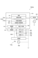
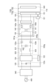
- FIG. 3 is a schematic diagram of a plasma processing apparatus according to an exemplary embodiment.
- the plasma processing apparatus 100A shown in FIG. 3 includes at least one high-frequency power source 300, a power receiving coil section 140, a power storage section 160, and at least one power consuming member 240 (see FIGS. 25 and 26).
- the plasma processing apparatus 100A may further include a power transmitting section 120, a power transmitting coil section 130, a rectifying/smoothing section 150, a constant voltage control section 180 (an example of a voltage control section), a ground frame 110, and a matching section 301.
- At least one high frequency power source 300 includes a first RF generating unit 31a and/or a second RF generating unit 31b. At least one high frequency power source 300 is electrically connected to the substrate support unit 11 via a matching unit 301.
- the matching unit 301 includes at least one impedance matching circuit.
- the ground frame 110 includes the chamber 10 and is electrically grounded.
- the ground frame 110 electrically separates the internal space 110h (RF-Hot space) from the external space 110a (atmospheric space).
- the ground frame 110 surrounds the substrate support section 11 disposed in the space 110h.
- the rectifier/smoothing section 150, the power storage section 160, and the constant voltage control section 180 are disposed in the space 110h.
- the power transmission section 120, the power transmission coil section 130, and the power receiving coil section 140 are disposed in the space 110a.
- the space 110h includes a reduced pressure space (vacuum space) and a non-reduced pressure space (non-vacuum space).
- the reduced pressure space is the space inside the chamber 10, and the non-reduced pressure space is the space outside the chamber 10.
- the substrate support section 11 and the substrate W are disposed in the reduced pressure space.
- the rectification/smoothing unit 150, the power storage unit 160, and the constant voltage control unit 180 are arranged in the non-reduced pressure space.
- the devices arranged in the space 110a i.e., the power transmission unit 120, the power transmission coil unit 130, and the power receiving coil unit 140, are covered by a metal housing made of a metal such as aluminum, and the metal housing is grounded. This suppresses leakage of high-frequency noise caused by high-frequency power such as the first RF signal (source RF signal) and/or the second RF signal (bias RF signal). There is an insulation distance between the metal housing and each power supply line.
- high-frequency power such as the first RF signal and/or the second RF signal that propagates toward the power transmission unit 120 may be referred to as high-frequency noise, common mode noise, or conductive noise.
- the power transmission unit 120 is electrically connected between the AC power source 400 (e.g., a commercial AC power source) and the power transmission coil unit 130.
- the power transmission unit 120 receives the frequency of AC power from the AC power source 400 and converts the frequency of the AC power to a transmission frequency, thereby generating AC power having the transmission frequency, i.e., transmission AC power.
- the power transmission coil section 130 includes a power transmission coil 131 (see FIG. 9 ), which will be described later.
- the power transmission coil 131 is electrically connected to the power transmission section 120.
- the power transmission coil 131 receives the transmitted AC power from the power transmission section 120, and wirelessly transmits the transmitted AC power to the power receiving coil 141.
- the receiving coil section 140 includes a receiving coil 141 (see FIG. 9) described later.
- the receiving coil 141 is electromagnetically inductively coupled to the transmitting coil 131.
- Electromagnetic inductive coupling includes magnetic field coupling and electric field coupling. Magnetic field coupling also includes magnetic field resonance (also called magnetic resonance).
- the distance between the receiving coil 141 and the transmitting coil 131 is set so as to suppress common mode noise (conductive noise).
- the distance between the receiving coil 141 and the transmitting coil 131 is set to a distance that allows power to be supplied.
- the distance between the receiving coil 141 and the transmitting coil 131 is set so that the attenuation of high frequency power (i.e., high frequency noise) between the receiving coil 141 and the transmitting coil 131 is equal to or less than a threshold, and so that the receiving coil 141 can receive power from the transmitting coil 131.
- the attenuation threshold is set to a value that can sufficiently prevent damage or malfunction of the transmitting section 120.
- the attenuation threshold is, for example, -20 dB.
- the transmitted AC power received by the receiving coil section 140 is output to the rectification and smoothing section 150.
- the rectification/smoothing unit 150 is electrically connected between the receiving coil unit 140 and the power storage unit 160.
- the rectification/smoothing unit 150 generates DC power by full-wave rectification and smoothing of the AC power transmitted from the receiving coil unit 140.
- the DC power generated by the rectification/smoothing unit 150 is stored in the power storage unit 160.
- the power storage unit 160 is electrically connected between the rectification/smoothing unit 150 and the constant voltage control unit 180.
- the rectification/smoothing unit 150 may generate DC power by half-wave rectification and smoothing of the AC power transmitted from the receiving coil unit 140.
- the rectification/smoothing unit 150 and the power transmission unit 120 are electrically connected to each other by a signal line 1250.
- the rectification/smoothing unit 150 transmits an instruction signal to the power transmission unit 120 via the signal line 1250.
- the instruction signal is a signal for instructing the power transmission unit 120 to supply or stop supplying the transmitted AC power.
- the instruction signal may include a status signal, an abnormality detection signal, and a cooling control signal for the power transmission coil unit 130 and the power receiving coil unit 140.
- the status signal is a value of the voltage, current, power magnitude and/or phase detected by the voltage detector 155v (see FIG. 14) and the current detector 155i (see FIG. 14) of the rectification/smoothing unit 150.
- the abnormality detection signal is a signal for transmitting the occurrence of a failure and/or temperature abnormality in the rectification/smoothing unit 150 to the power transmission unit 120.
- the cooling control signal controls the cooling mechanism provided in the power transmission coil unit 130 and the power receiving coil unit 140.
- the cooling control signal controls, for example, the fan speed in the case of air cooling, or the flow rate and/or temperature of the refrigerant in the case of liquid cooling.
- the constant voltage control unit 180 applies a voltage to at least the power consuming member 240 using the power stored in the power storage unit 160.
- the constant voltage control unit 180 can control the application of voltage to at least the power consuming member 240 and the stopping of the application.
- the receiving coil 141 functions as a filter against high-frequency noise caused by high-frequency power such as the first RF signal and/or the second RF signal. Therefore, the propagation of high-frequency noise to a power source external to the plasma processing apparatus is suppressed.
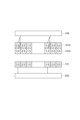
- FIG. 4 is a schematic diagram of a plasma processing apparatus according to another exemplary embodiment.
- the plasma processing apparatus 100B shown in FIG. 4 will be described below in terms of its differences from the plasma processing apparatus 100A.
- the plasma processing apparatus 100B further includes a voltage control converter 170.
- the voltage control converter 170 is a DC-DC converter, and is connected between the power storage unit 160 and the constant voltage control unit 180.
- the voltage control converter 170 can be configured to input a constant output voltage to the constant voltage control unit 180 even if a voltage fluctuation occurs in the power storage unit 160.
- the voltage fluctuation in the power storage unit 160 can occur as a voltage drop corresponding to the stored power, for example, when the power storage unit 160 is configured as an electric double layer.
- FIG. 5 is a schematic diagram of a plasma processing apparatus according to yet another exemplary embodiment.
- the plasma processing apparatus 100C shown in FIG. 5 will be described below in terms of its differences from the plasma processing apparatus 100B.
- the plasma processing apparatus 100C further includes an RF filter 190.
- the RF filter 190 is connected between the rectification/smoothing unit 150 and the power transmission unit 120.
- the RF filter 190 constitutes part of the signal line 1250.
- the RF filter 190 has a characteristic of suppressing the propagation of high-frequency power (high-frequency noise) via the signal line 1250.
- the RF filter 190 includes a low-pass filter that has a high impedance to high-frequency noise (conductive noise) but has a characteristic of passing instruction signals of relatively low frequencies.
- the power storage unit 160, the voltage control converter 170, and the constant voltage control unit 180 are integrated with each other. That is, the power storage unit 160, the voltage control converter 170, and the constant voltage control unit 180 are all disposed in a single metal housing or formed on a single circuit board. This shortens the length of each of the pair of power supply lines (positive and negative lines) connecting the power storage unit 160 and the voltage control converter 170 to each other. It is also possible to make the lengths of the pair of power supply lines connecting the power storage unit 160 and the voltage control converter 170 to each other equal. It is also possible to shorten the length of each of the pair of power supply lines (positive and negative lines) connecting the voltage control converter 170 and the constant voltage control unit 180 to each other.
- FIG. 6 is a schematic diagram of a plasma processing apparatus according to yet another exemplary embodiment.
- the plasma processing apparatus 100D shown in FIG. 6 will be described below from the viewpoint of the differences from the plasma processing apparatus 100C.
- the plasma processing apparatus 100D does not include an RF filter 190.
- the rectification/smoothing unit 150 includes a communication unit 151, which is a wireless unit.
- the communication unit 151 is disposed in the non-reduced pressure space.
- the power transmission unit 120 also includes a communication unit 121, which is a wireless unit.
- the communication unit 121 is disposed in the space 110a.
- the above-mentioned instruction signal is transmitted between the rectification/smoothing unit 150 and the power transmission unit 120 using the communication unit 151 and the communication unit 121. Details of the communication unit 121 and the communication unit 151 will be described later.
- FIG. 7 is a schematic diagram of a plasma processing apparatus according to yet another exemplary embodiment.
- the plasma processing apparatus 100E shown in FIG. 7 will be described below in terms of its differences from the plasma processing apparatus 100D.
- the plasma processing apparatus 100E further includes an RF filter 200.
- the RF filter 200 is connected between the receiving coil section 140 and the rectification and smoothing section 150.
- the RF filter 200 has the characteristic of reducing or blocking high-frequency noise propagating from the receiving coil section 140 to the transmitting coil 131 and the transmitting section 120. Details of the RF filter 200 will be described later.
- FIG. 8 is a diagram illustrating a power transmission unit according to one exemplary embodiment.
- the power transmission unit 120 receives the frequency of AC power from the AC power source 400 and converts the frequency of the AC power to a transmission frequency, thereby generating transmission AC power having the transmission frequency.
- the power transmission unit 120 includes a control unit 122, a rectification and smoothing unit 123, and an inverter 124.
- the control unit 122 is composed of a processor such as a CPU or a programmable logic device such as an FPGA (Field-Programmable Gate Array).
- the rectification/smoothing unit 123 includes a rectification circuit and a smoothing circuit.
- the rectification circuit includes, for example, a diode bridge.
- the smoothing circuit includes, for example, a line capacitor.
- the rectification/smoothing unit 123 generates DC power by full-wave rectification and smoothing of the AC power from the AC power supply 400.
- the rectification/smoothing unit 123 may also generate DC power by half-wave rectification and smoothing of the AC power from the AC power supply 400.
- the inverter 124 generates transmission AC power having a transmission frequency from the DC power output by the rectification and smoothing unit 123.
- the inverter 124 is, for example, a full-bridge inverter, and includes multiple triacs or multiple switching elements (for example, FETs).
- the inverter 124 generates transmission AC power by ON/OFF control of the multiple triacs or multiple switching elements by the control unit 122.
- the transmission AC power output from the inverter 124 is output to the power transmission coil unit 130.
- the power transmission unit 120 may further include a voltage detector 125v, a current detector 125i, a voltage detector 126v, and a current detector 126i.
- the voltage detector 125v detects a voltage value between a pair of power supply lines connecting the rectification and smoothing unit 123 and the inverter 124.
- the current detector 125i detects a current value between the rectification and smoothing unit 123 and the inverter 124.
- the voltage detector 126v detects a voltage value between a pair of power supply lines connecting the inverter 124 and the power transmission coil unit 130.
- the current detector 126i detects a current value between the inverter 124 and the power transmission coil unit 130.
- the voltage value detected by the voltage detector 125v, the current value detected by the current detector 125i, the voltage value detected by the voltage detector 126v, and the current value detected by the current detector 126i are notified to the control unit 122.
- the power transmission unit 120 includes the communication unit 121 described above.
- the communication unit 121 includes a driver 121d, a transmitter 121tx, and a receiver 121rx.
- the transmitter 121tx is a transmitter of a wireless signal or a transmitter of an optical signal.
- the receiver 121rx is a receiver of a wireless signal or a receiver of an optical signal.
- the communication unit 121 drives the transmitter 121tx using the driver 121d to output a signal from the control unit 122 from the transmitter 121tx as a wireless signal or an optical signal.
- the signal output from the transmitter 121tx is received by the communication unit 151 (see FIG. 14) described later.
- the communication unit 121 receives a signal such as the instruction signal described above from the communication unit 151 using the receiver 121rx, and inputs the received signal to the control unit 122 via the driver 121d.
- the control unit 122 switches between outputting and stopping the transmitted AC power by controlling the inverter 124 according to the instruction signal received from the communication unit 151 via the communication unit 121, the voltage value detected by the voltage detector 125v, the current value detected by the current detector 125i, the voltage value detected by the voltage detector 126v, and the current value detected by the current detector 126i.
- FIG. 9 to FIG. 11 is a diagram showing a power transmission coil section and a power receiving coil section according to an exemplary embodiment.
- the power transmission coil section 130 may include a resonant capacitor 132a and a resonant capacitor 132b in addition to the power transmission coil 131.
- the resonant capacitor 132a is connected between one of a pair of power supply lines connecting the power transmission section 120 and the power transmission coil section 130 and one end of the power transmission coil 131.
- the resonant capacitor 132b is connected between the other of the pair of power supply lines and the other end of the power transmission coil 131.
- the power transmission coil 131, the resonant capacitor 132a, and the resonant capacitor 132b form a resonant circuit for the transmission frequency. That is, the power transmission coil 131, the resonant capacitor 132a, and the resonant capacitor 132b have a resonant frequency that is approximately equal to the transmission frequency. Note that the power transmission coil section 130 may not include either the resonant capacitor 132a or the resonant capacitor 132b.
- the power transmission coil section 130 may further include a metal housing 130g.
- the metal housing 130g has an open end and is grounded.
- the power transmission coil 131 is arranged in the metal housing 130g with an insulating distance secured.
- the power transmission coil section 130 may further include a heat sink 134, a ferrite material 135, and a thermally conductive sheet 136.
- the heat sink 134 is arranged in the metal housing 130g and is supported by the metal housing 130g.
- the ferrite material 135 is arranged on the heat sink 134.
- the thermally conductive sheet 136 is arranged on the ferrite material 135.
- the power transmission coil 131 is arranged on the thermally conductive sheet 136 and faces the power receiving coil 141 through the open end of the metal housing 130g.
- a resonant capacitor 132a and a resonant capacitor 132b may further be accommodated in the metal housing 130g.
- the receiving coil section 140 includes a receiving coil 141.
- the receiving coil 141 is electromagnetically inductively coupled to the transmitting coil 131.
- the receiving coil section 140 may include a resonant capacitor 142a and a resonant capacitor 142b in addition to the receiving coil 141.
- the resonant capacitor 142a is connected between one of a pair of power supply lines extending from the receiving coil section 140 and one end of the receiving coil 141.
- the resonant capacitor 142b is connected between the other of the pair of power supply lines and the other end of the receiving coil 141.
- the receiving coil 141, the resonant capacitor 142a, and the resonant capacitor 142b form a resonant circuit for the transmission frequency.
- the receiving coil 141, the resonant capacitor 142a, and the resonant capacitor 142b have a resonant frequency that is approximately equal to the transmission frequency.
- the receiving coil section 140 may not include either the resonant capacitor 142a or the resonant capacitor 142b.
- the receiving coil section 140 may further include a metal housing 140g.
- the metal housing 140g has an open end and is grounded.
- the receiving coil 141 is arranged in the metal housing 140g with an insulating distance secured.
- the receiving coil section 140 may further include a spacer 143, a heat sink 144, a ferrite material 145, and a thermally conductive sheet 146.
- the spacer 143 is arranged in the metal housing 140g and is supported by the metal housing 140g. The spacer 143 will be described later.
- the heat sink 144 is arranged on the spacer 143.
- the ferrite material 145 is arranged on the heat sink 144.
- the thermally conductive sheet 146 is arranged on the ferrite material 145.
- the receiving coil 141 is arranged on the thermally conductive sheet 146 and faces the transmitting coil 131 through the open end of the metal housing 140g. As shown in FIG. 11, resonant capacitor 142a and resonant capacitor 142b may be further housed within metal housing 140g.
- the spacer 143 is made of a dielectric material and is provided between the receiving coil 141 and the metal housing 140g (ground).
- the spacer 143 provides a spatial stray capacitance between the receiving coil 141 and the ground.
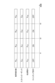
- FIG. 12 is a graph showing impedance characteristics of the power receiving coil unit according to one exemplary embodiment.
- FIG. 12 shows impedance characteristics of the power receiving coil unit 140 according to the thickness of the spacer 143.
- the thickness of the spacer 143 corresponds to the distance between the heat sink 144 and the metal housing 140g.
- the power receiving coil unit 140 can adjust the impedance of each of the frequencies fH and fL according to the thickness of the spacer 143. Therefore, according to the power receiving coil unit 140, it is possible to provide a high impedance at each of the two frequencies of high frequency power used in the plasma processing apparatus, such as the first RF signal and the second RF signal.
- a high impedance can be obtained in the power receiving coil unit 140, it is possible to suppress the loss of high frequency power and obtain a high processing rate (e.g., an etching rate).
- FIG. 13 is a diagram showing an RF filter according to an exemplary embodiment.
- the RF filter 200 is connected between the receiving coil section 140 and the rectification and smoothing section 150.
- the RF filter 200 includes an inductor 201a, an inductor 201b, a termination capacitor 202a, and a termination capacitor 202b.
- One end of the inductor 201a is connected to the resonant capacitor 142a, and the other end of the inductor 201a is connected to the rectification and smoothing section 150.
- One end of the inductor 201b is connected to the resonant capacitor 142b, and the other end of the inductor 201b is connected to the rectification and smoothing section 150.
- the termination capacitor 202a is connected between one end of the inductor 201a and the ground.
- the termination capacitor 202b is connected between one end of the inductor 201b and the ground.
- the inductor 201a and the termination capacitor 202a form a low-pass filter.
- the inductor 201b and the termination capacitor 202b form a low-pass filter.
- the RF filter 200 provides high impedance at each of the two high-frequency power frequencies used in the plasma processing apparatus, such as the first RF signal and the second RF signal. This suppresses the loss of high-frequency power, allowing a high processing rate (e.g., etching rate) to be obtained.
- FIG. 14 is a diagram showing a rectifying/smoothing unit according to an exemplary embodiment.
- the rectifying/smoothing unit 150 includes a control unit 152, a rectifying circuit 153, and a smoothing circuit 154.
- the rectifying circuit 153 is connected between the receiving coil unit 140 and the smoothing circuit 154.
- the smoothing circuit 154 is connected between the rectifying circuit 153 and the power storage unit 160.
- the control unit 152 is composed of a processor such as a CPU or a programmable logic device such as an FPGA (Field-Programmable Gate Array). Note that the control unit 152 may be the same as the control unit 122 or may be different.
- the rectifier circuit 153 outputs power generated by full-wave rectification of the AC power from the power receiving coil unit 140.
- the rectifier circuit 153 is, for example, a diode bridge.
- the rectifier circuit 153 may also output power generated by half-wave rectification of the AC power from the power receiving coil unit 140.
- the smoothing circuit 154 generates DC power by smoothing the power from the rectifier circuit 153.
- the smoothing circuit 154 may include an inductor 1541a, a capacitor 1542a, and a capacitor 1542b.
- One end of the inductor 1541a is connected to one of a pair of inputs of the smoothing circuit 154.
- the other end of the inductor 1541a is connected to a positive output (V OUT+ ) of the rectifier/smoothing unit 150.
- the positive output of the rectifier/smoothing unit 150 is connected to one end of each of one or more capacitors of the power storage unit 160 via a positive line 160p (see FIG. 23(a) and FIG. 23(b)) of a pair of power supply lines described later.
- One end of the capacitor 1542a is connected to one of the pair of inputs of the smoothing circuit 154 and one end of the inductor 1541a.
- the other end of the capacitor 1542a is connected to the other of the pair of outputs of the smoothing circuit 154 and the negative output (V OUT- ) of the rectifying and smoothing unit 150.
- the negative output of the rectifying and smoothing unit 150 is connected to the other end of each of one or more capacitors of the power storage unit 160 via a negative line 160m (see FIG. 23(a) and FIG. 23(b)) of a pair of power supply lines described later.
- One end of the capacitor 1542b is connected to the other end of the inductor 1541a.
- the other end of the capacitor 1542b is connected to the other of the pair of outputs of the smoothing circuit 154 and the negative output (V OUT- ) of the rectifying and smoothing unit 150.
- the rectification/smoothing unit 150 may further include a voltage detector 155v and a current detector 155i.
- the voltage detector 155v detects a voltage value between the positive output and the negative output of the rectification/smoothing unit 150.
- the current detector 155i detects a current value between the rectification/smoothing unit 150 and the power storage unit 160.
- the voltage value detected by the voltage detector 155v and the current value detected by the current detector 155i are notified to the control unit 152.
- the control unit 152 generates the above-mentioned instruction signal according to the power stored in the power storage unit 160.
- the control unit 152 when the power stored in the power storage unit 160 is equal to or less than a first threshold, the control unit 152 generates an instruction signal for instructing the power transmission unit 120 to supply power, i.e., to output the transmitted AC power.
- the first threshold is, for example, the power consumption at a load such as the power consumption member 240.
- the first threshold may be a value obtained by multiplying the power consumption at a load such as the power consumption member 240 by a certain value (for example, a value in the range of 1 to 3) in consideration of a margin.
- the control unit 152 when the power stored in the power storage unit 160 is greater than the second threshold, the control unit 152 generates an instruction signal to instruct the power transmission unit 120 to stop power supply, i.e., to stop outputting transmitted AC power.
- the second threshold is a value that does not exceed the limit storage power of the power storage unit 160.
- the second threshold is, for example, a value obtained by multiplying the limit storage power of the power storage unit 160 by a certain value (for example, a value equal to or less than 1).
- the rectifying and smoothing unit 150 includes the communication unit 151 described above.
- the communication unit 151 includes a driver 151d, a transmitter 151tx, and a receiver 151rx.
- the transmitter 151tx is a wireless signal transmitter or an optical signal transmitter.
- the receiver 151rx is a wireless signal receiver or an optical signal receiver.
- the communication unit 151 drives the transmitter 151tx with the driver 151d to output a signal from the control unit 122, such as an instruction signal, as a wireless signal or an optical signal from the transmitter 151tx.
- the signal output from the transmitter 151tx is received by the communication unit 121 of the power transmission unit 120.
- the communication unit 151 also receives a signal from the communication unit 121 with the receiver 151rx, and inputs the received signal to the control unit 152 via the driver 151d.
- FIG. 15 is a diagram showing an RF filter 190 according to an exemplary embodiment.
- the signal line 1250 may include a first signal line electrically connecting the signal output (Tx) of the power transmission unit 120 and the signal input (Rx) of the rectification and smoothing unit 150, and a second signal line electrically connecting the signal input (Rx) of the power transmission unit 120 and the signal output (Tx) of the rectification and smoothing unit 150.
- the signal line 1250 may include a signal line connecting the first reference voltage terminal (VCC) of the power transmission unit 120 and the first reference voltage terminal (VCC) of the rectification and smoothing unit 150, and a signal line connecting the second reference voltage terminal (GND) of the power transmission unit 120 and the second reference voltage terminal (GND) of the rectification and smoothing unit 150.
- the signal line 1250 may be a shielded cable covered with a shield at ground potential. In this case, the multiple signal lines constituting the signal line 1250 may be individually covered with a shield, or may be collectively covered with a shield.
- the RF filter 190 provides a low-pass filter for each of the multiple signal lines constituting the signal line 1250.
- the low-pass filter may be an LC filter including an inductor and a capacitor.
- the inductor of the low-pass filter constitutes a part of the corresponding signal line.
- the capacitor is connected between one end of the inductor connected to the power transmission unit 120 and the ground.
- the RF filter 190 makes it possible to suppress the propagation of high-frequency power (high-frequency noise) via the signal line 1250 between the rectification/smoothing unit 150 and the power transmission unit 120.
- Figure 16 is a diagram showing a communication unit of the power transmission unit and a communication unit of the rectification and smoothing unit according to one exemplary embodiment.
- Figures 17 and 18 are diagram showing a plasma processing apparatus according to yet another exemplary embodiment.
- the communication unit 121 and the communication unit 151 may be configured to transmit signals such as the above-mentioned instruction signal between each other via wireless communication.
- the communication via wireless communication may be performed by optical communication.
- the communication unit 121 and the communication unit 151 transmit signals between them via wireless communication, the communication unit 121 and the communication unit 151 may be disposed in any position as long as there is no shield between them.
- the RF filter 190 is not required.
- the signal line 1250 may be a shielded cable covered with a shield at ground potential.
- the multiple signal lines that make up signal line 1250 may be individually covered with a shield or may be collectively covered with a shield.
- Fig. 19 is a diagram showing a communication unit of the power transmission unit and a communication unit of the rectification and smoothing unit according to another exemplary embodiment.
- Figs. 20 to 22 are each a diagram showing a schematic diagram of a plasma processing apparatus according to yet another exemplary embodiment.
- the communication unit 121 and the communication unit 151 may be configured to transmit a signal (optical signal) such as the above-mentioned instruction signal between them via the optical fiber 1260, that is, by optical fiber communication.
- a signal optical signal
- the communication unit 121 and the communication unit 151 transmit a signal between them via the optical fiber 1260
- the communication unit 121 and the communication unit 151 may be disposed at any position as long as the bending radius of the optical fiber 1260 is within an allowable range.
- the RF filter 190 is not required.
- FIG. 23(a) and FIG. 23(b) are diagram showing a power storage unit according to an exemplary embodiment.
- the power storage unit 160 includes a capacitor 161.
- the capacitor 161 is connected between a pair of power supply lines, that is, a positive line 160p and a negative line 160m.
- the positive line 160p extends from the positive output (V OUT+ ) of the rectifying and smoothing unit 150 toward the load.
- the negative line 160m extends from the negative output (V OUT- ) of the rectifying and smoothing unit 150 toward the load.
- the capacitor 161 may be a polarized capacitor.
- the capacitor 161 may be an electric double layer or a lithium ion battery.
- the power storage unit 160 may include a plurality of capacitors 161.
- the plurality of capacitors 161 are connected in series between a positive line 160p and a negative line 160m.
- the plurality of capacitors 161 may have the same capacitance or may have different capacitances.
- Each of the plurality of capacitors 161 may be a polarized capacitor.
- Each of the plurality of capacitors 161 may be an electric double layer or a lithium ion battery.
- the power storage unit 160 must be used under conditions in which the sum of the input voltage and the line potential difference due to normal mode noise is lower than the allowable input voltage.
- the power storage unit 160 includes a plurality of capacitors 161 connected in series, the allowable input voltage of the power storage unit 160 is increased. Therefore, according to the example shown in FIG. 23B, the noise resistance of the power storage unit 160 is improved.
- FIG. 24 is a diagram showing a voltage controlled converter according to an exemplary embodiment.
- the voltage controlled converter 170 is a DC-DC converter.
- the voltage controlled converter 170 is connected between the power storage unit 160 and the constant voltage control unit 180.
- a positive line 160p is connected to the positive input (V IN+ ) of the voltage controlled converter 170.
- a negative line 160m is connected to the negative input (V IN- ) of the voltage controlled converter 170.
- a positive output (V OUT+ ) of the voltage controlled converter 170 is connected to the positive input (V IN+ ) of the constant voltage control unit 180.
- a negative output (V OUT- ) of the voltage controlled converter 170 is connected to the negative input (V IN- ) of the constant voltage control unit 180.
- the voltage controlled converter 170 may include a control unit 172, a low-pass filter 173, a transformer 174, and a capacitor 175.
- the low-pass filter 173 may include an inductor 1731a, a capacitor 1732a, and a capacitor 1732b.
- One end of the inductor 1731a is connected to the positive input (V IN+ ) of the voltage controlled converter 170.
- the other end of the inductor 1731a is connected to one end of the primary coil of the transformer 174.
- One end of the capacitor 1732a is connected to one end of the inductor 1731a and the positive input (V IN+ ) of the voltage controlled converter 170.
- the other end of the capacitor 1732a is connected to the negative input (V IN- ) of the voltage controlled converter 170.
- One end of the capacitor 1732b is connected to the other end of the inductor 1731a.
- the other end of the capacitor 1732b is connected to the negative input (V IN- ) of the voltage controlled converter
- the transformer 174 includes a primary coil 1741, a secondary coil 1742, and a switch 1743.
- the other end of the primary coil 1741 is connected to the negative input (V IN ⁇ ) of the voltage controlled converter 170 via the switch 1743.
- One end of the secondary coil 1742 is connected to one end of the capacitor 175 and the positive output (V OUT+ ) of the voltage controlled converter 170.
- the other end of the secondary coil 1742 is connected to the other end of the capacitor 175 and the negative output (V OUT ⁇ ) of the voltage controlled converter 170.
- a driver 1744 is connected to the switch 1743.
- the driver 1744 opens and closes the switch 1743.
- the switch 1743 is closed, that is, when the other end of the primary coil 1741 and the negative input (V IN- ) are in a conductive state, the other end of the primary coil 1741 is connected to the negative input (V IN- ) of the voltage control converter 170, and DC power from the voltage control converter 170 is provided to the constant voltage control unit 180.
- the voltage-controlled converter 170 may further include a voltage detector 176v and a current detector 176i.
- the voltage detector 176v detects the voltage value between both ends of the secondary coil 1742 or the voltage value between the positive output and the negative output of the voltage-controlled converter 170.
- the current detector 176i measures the current value between the other end of the secondary coil 1742 and the negative output of the voltage-controlled converter 170.
- the voltage value detected by the voltage detector 176v and the current value detected by the current detector 176i are notified to the control unit 172.
- the control unit 172 may be the same as at least one of the control unit 122 and the control unit 152, or may be different.
- the control unit 172 controls the driver 1744 to cut off the supply of DC power from the voltage controlled converter 170 to the constant voltage control unit 180.
- the voltage value between the positive output and negative output of the voltage controlled converter 170 is the sum of the output voltage value of the voltage controlled converter 170 and the line potential difference due to normal mode noise. In this embodiment, damage to the load of the voltage controlled converter 170 due to overvoltage caused by the line potential difference due to normal mode noise can be suppressed.
- Figs. 25 and 26 are diagrams illustrating a constant voltage control unit according to some exemplary embodiments.
- the constant voltage control unit 180 is connected between the power storage unit 160 and at least one power consuming member 240, and is configured to control application of voltage (application of DC voltage) to at least one power consuming member 240 and its stop.
- the constant voltage control unit 180 includes a control unit 182 and at least one switch 183.
- the positive input (V IN+ ) of the constant voltage control unit 180 is connected to the power consuming member 240 via the switch 183.
- the negative input (V IN- ) of the constant voltage control unit 180 is connected to the power consuming member 240.
- the switch 183 is controlled by the control unit 182. When the switch 183 is closed, a DC voltage from the constant voltage control unit 180 is applied to the power consuming member 240. When the switch 183 is opened, application of the DC voltage from the constant voltage control unit 180 to the power consuming member 240 is stopped.
- the control unit 182 may be the same as or different from at least one of the control units 122, 152, and 172.
- the plasma processing apparatus includes a plurality of power consuming members 240.
- the constant voltage control unit 180 includes a control unit 182 and a plurality of switches 183.
- the positive input (V IN+ ) of the constant voltage control unit 180 is connected to the plurality of power consuming members 240 via the plurality of switches 183.
- the negative input (V IN ⁇ ) of the constant voltage control unit 180 is connected to the plurality of power consuming members 240.
- the multiple power consumption members 240 may include multiple heaters (resistance heating elements).
- the multiple heaters may be provided within the substrate support portion 11.
- multiple resistors 260 are arranged near each of the multiple heaters.
- Each of the multiple resistors 260 has a resistance value that changes with temperature.
- Each of the multiple resistors 260 is, for example, a thermistor.
- Each of the multiple resistors 260 is connected in series with a reference resistor (not shown).
- the constant voltage control unit 180 includes multiple measurement units 184.
- Each of the multiple measurement units 184 applies a reference voltage to the series connection of a corresponding resistor among the multiple resistors 260 and a reference resistor to detect the voltage value between both ends of the resistor.
- Each of the multiple measurement units 184 notifies the control unit 182 of the detected voltage value.
- the control unit 182 identifies the temperature of the area in which the corresponding heater is located from the notified voltage value, and controls the application of DC voltage to the corresponding heater so that the temperature of the area approaches the target temperature.
- an optical fiber thermometer may be placed in place of the multiple resistors 260. In this case, wiring between the multiple resistors 260 and the multiple measuring units 184 is not required, and the effect of high-frequency conductive noise on the power consuming member 240 can be eliminated.
- the constant voltage control unit 180 includes a voltage detector 185v and a plurality of current detectors 185i.
- the voltage detector 185v detects the voltage value applied to each of the plurality of heaters.
- the plurality of current detectors 185i measure the value of the current supplied to a corresponding one of the plurality of heaters, i.e., the current value.
- the plurality of measurement units 184 identify the resistance value of a corresponding one of the plurality of heaters from the current value detected by the corresponding one of the plurality of current detectors 185i and the voltage value detected by the voltage detector 185v.
- the control unit 182 identifies the temperature of each of the plurality of regions in which the plurality of heaters are disposed, from the detected resistance value of each of the plurality of heaters.
- the control unit 182 controls the application of a DC voltage to each of the plurality of heaters so as to bring the temperature of each of the plurality of regions closer to the target temperature.
- FIG. 27 is a schematic diagram of a plasma processing apparatus according to yet another exemplary embodiment.
- the plasma processing apparatus 100G shown in FIG. 27 will be described below from the viewpoint of the differences from the plasma processing apparatus 100E shown in FIG. 7.
- the plasma processing apparatus 100G does not include a power storage unit 160.
- the rectification/smoothing unit 150 is connected to the constant voltage control unit 180 without passing through the power storage unit 160 and the voltage control converter 170. That is, in the plasma processing apparatus 100E, the power generated by the rectification/smoothing unit 150 is supplied from the constant voltage control unit 180 to at least one power consumption member 240 without passing through the power storage unit 160 and the voltage control converter 170.
- the constant voltage control unit 180 controls application and stop of voltage to each of the plurality of power consuming members 240. Therefore, in the plasma processing apparatus 1, the load receiving power from the rectification/smoothing unit 150 via the constant voltage control unit 180 fluctuates. That is, the load resistance value R L fluctuates.
- the control unit 122 of the power transmitting unit 120 detects the input impedance Z in of the power transmitting unit 120. As a result, the control unit 122 detects the load fluctuation, determines a required power level according to the input impedance Z in or the load resistance value R L , and adjusts the output power from the power transmitting unit 120.
- Fig. 28 is a diagram showing an example of an equivalent circuit of the power transmitting coil section and the power receiving coil section in a state where the power transmitted from the power transmitting section 120 is resonating at the transmission frequency and the phase difference between the input voltage Vin and the input current Iin is zero (power factor 100%). As shown in Fig.
- the equivalent circuit of the power transmitting coil section and the power receiving coil includes, in one example, a power transmitting coil 131 having a self-inductance L1 , a load resistance of the power transmitting coil 131 having a load resistance value R1 , a resonant capacitor of the power transmitting coil section 130 having a capacitance C1 , three inductors between the power transmitting coil 131 and the power receiving coil 141 having a mutual inductance Lm , a power receiving coil 141 having a self-inductance L2 , a load resistance of the power receiving coil 141 having a load resistance value R2 , and a resonant capacitor of the power receiving coil section 140 having a capacitance C2 .
- a power transmitting coil 131 having a self-inductance L1 a load resistance of the power transmitting coil 131 having a load resistance value R1
- a resonant capacitor of the power transmitting coil section 130 having a capacitance C1
- Zin is the input impedance of the power transmitting unit 120
- Vin is the input voltage from the power transmitting unit 120 to the power transmitting coil unit 130
- Iin is the input current from the power transmitting unit 120 to the power transmitting coil unit 130.
- the input impedance Zin is defined by the following formula (1).
- f is the transmission frequency of the power transmitted from power transmitting unit 120.
- the control unit 122 determines the effective value of the input voltage Vin from the voltage measured by the voltage detector 126v, and determines the effective value of the input current Iin from the current measured by the current detector 126i.
- the control unit 122 can determine the input impedance Zin from the input voltage Vin and the input current Iin using equation (1).
- the control unit 122 may further determine the load resistance value RL from the input impedance Zin using equation (1).
- the control unit 122 calculates a required power level according to a parameter value, which is the input impedance Zin or the load resistance value R L , by using at least one table.
- the control unit 122 may specify a peak value V P of the output voltage V out of the power transmitting unit 120, a duty ratio Duty of the output voltage V out , and an amplitude I A of the output current I out as parameters for specifying a required power level of the output power from the power transmitting unit 120.
- at least one table is stored in a storage device 122m (see FIG. 31 ), such as a memory device connected to the control unit 122.
- the storage device 122m may be a part of the power transmitting unit 120.
- Each of Fig. 29 and Fig. 30 is a diagram showing an example of at least one of the tables.
- the control unit 122 can use a single table stored in the storage device 122m. As shown in Fig. 29, the table stores a peak value V P , a duty ratio Duty, and an amplitude I A in association with the input impedance Z in .
- the control unit 122 can specify the required power level according to the input impedance Z in , that is, the peak value V P , the duty ratio Duty, and the amplitude I A , by referring to the table shown in Fig. 29 using the input impedance Z in as a key.
- the control unit 122 controls each unit of the power transmitting unit 120 to output an output power having a peak value V P and a duty ratio Duty of the output voltage V out and an amplitude I A of the output current I out.
- the control unit 122 may obtain the load resistance value R L by formula (1) based on the transmission frequency f, the mutual inductance Lm , the load resistance value R 1 , the load resistance value R 2 , and the input impedance Z in .
- 2 ⁇ f may be stored in the storage device 122m instead of the transmission frequency f.
- the storage device 122m may store the self-inductance L 1 of the power transmitting coil 131, the self-inductance L 2 of the power receiving coil 141, and the coupling coefficient k between the power transmitting coil 131 and the power receiving coil 141 instead of the mutual inductance L m, and the control unit 122 may calculate the mutual inductance L m from the self-inductance L 1 , the self-inductance L 2 , and the coupling coefficient k.
- the storage device 122m may store 2 ⁇ fLm or ( 2 ⁇ fLm ) 2 instead of the transmission frequency f and the mutual inductance Lm .
- the table stores a peak value V P , a duty ratio Duty, and an amplitude I A in association with a load resistance value R L.
- the control unit 122 can specify the required power level according to the load resistance value R L , that is, the peak value V P , the duty ratio Duty, and the amplitude I A , by referring to the table shown in FIG. 30 using the load resistance value R L as a key.
- the control unit 122 controls each unit of the power transmitting unit 120 to output output power having a peak value V P and a duty ratio Duty of the output voltage V out and an amplitude I A of the output current I out .
- the distance (gap length) between the power transmitting coil 131 and the power receiving coil 141 is variable as described below, multiple tables similar to the tables shown in FIG. 29 or FIG. 30 are stored in the memory device 122m. Each of the multiple tables is prepared for each of the multiple settable distances between the power transmitting coil 131 and the power receiving coil 141. The control unit 122 can select the table to use depending on the current distance between the power transmitting coil 131 and the power receiving coil 141.
- the plasma processing apparatus 100G is capable of supplying electric power by electromagnetic induction coupling without going through a power storage unit in accordance with the load resistance value R L of the power consuming member 240. That is, the plasma processing apparatus 100G is capable of supplying electric power in accordance with the fluctuation in the load resistance value R L of the power consuming member 240 (hereinafter sometimes referred to as "load fluctuation") by electromagnetic induction coupling without going through a power storage unit.
- load fluctuation the fluctuation in the load resistance value R L of the power consuming member 240
- the control unit 122 can specify the fluctuation of the load resistance value R L by calculating the input impedance Z in , it is not necessary to issue a power change instruction from the constant voltage control unit 180 via the communication unit 151 and the communication unit 121.
- the power change instruction may be notified to the control unit 122 in advance via the communication unit 151 and the communication unit 121 before the load fluctuation occurs.
- this load fluctuation may be performed by the constant voltage control unit 180 at a timing synchronized with the output power having the transmission frequency f output from the power receiving coil unit 140.
- a synchronization signal synchronized with the output power having the transmission frequency f from the power receiving coil unit 140 may be generated by the rectification and smoothing unit 150, and the constant voltage control unit 180 may cause the load fluctuation at a timing synchronized with the output power using this synchronization signal.
- the load fluctuation may be set not to occur simultaneously with the change in the distance between the power transmitting coil 131 and the power receiving coil 141.
- FIG. 31 is a schematic diagram of a plasma processing apparatus according to yet another exemplary embodiment.
- the plasma processing apparatus 100G may include an excess power consumption circuit 500.
- the excess power consumption circuit 500 may include a line capacitor 501, an excess power consumption load 502, and a switching element 503.
- the line capacitor 501 can be connected via a switching element 503 between a pair of power supply lines, i.e., a positive line and a negative line, that connect the rectification and smoothing unit 150 and the constant voltage control unit 180 to each other. Specifically, one end of the line capacitor 501 is connected to the switching element 503, and the other end of the line capacitor 501 is connected to the negative line.
- a pair of power supply lines i.e., a positive line and a negative line
- the excess power consumption load 502 is a load for consuming the power stored in the line capacitor 501.
- the excess power consumption load 502 can consume power by converting the power into heat.
- the excess power consumption load 502 may be provided with a cooling mechanism such as a fan for cooling the excess power consumption load 502.
- the excess power consumption load 502 can be selectively connected to the line capacitor 501 via the switching element 503. One end of the excess power consumption load 502 is connected to the switching element 503, and the other end of the excess power consumption load 502 is connected to the negative line.
- the switching element 503 When the switching element 503 is in the ON state, it cuts off the connection between the line capacitor 501 and the excess power consumption load 502, and connects one end of the line capacitor 501 to the positive line. When the switching element 503 is in the OFF state, it cuts off the connection between one end of the line capacitor 501 and the positive line, and connects one end of the line capacitor 501 to one end of the excess power consumption load 502. From the viewpoint of high-speed response, a semiconductor switching element may be used as the switching element 503.
- FIG. 32 is a timing chart showing an example of the load resistance value, input impedance, transmission power, and state of the switching element.
- the control unit 182 of the constant voltage control unit 180 sets the state of the switching element 503 to ON when a load fluctuation occurs, particularly when the load resistance value R L is to be reduced.
- the control unit 182 sets the state of the switching element 503 to OFF after the level of the power transmitted from the power transmitting unit 120 is changed to a power level corresponding to the load resistance value R L.
- the load resistance value R L changes from the load resistance value R LA to the load resistance value R LB , and the state of the switching element 503 is changed from OFF to ON.
- the input impedance Z in obtained in the control unit 122 of the power transmitting unit 120 before time t2 is Z inA corresponding to the load resistance value R LA . Therefore, the transmission power before time t2 is P inA .
- the input impedance Zin obtained in the control unit 122 of the power transmitting unit 120 at time t2 becomes ZinB corresponding to the load resistance value RLB . Then, in the example of Fig. 32, when the input impedance ZinB is detected, the transmission power changes from PinA to PinB at a later time t3 , and the state of the switching element 503 is set to OFF.
- the excess power consumption circuit 500 With the excess power consumption circuit 500, power is temporarily stored in the line capacitor 501 after a load fluctuation occurs and before the power level is changed. This prevents a large current from flowing into the constant voltage control unit 180 and the power consumption member 240, and can prevent damage to the constant voltage control unit 180 and the power consumption member 240. Furthermore, with the excess power consumption circuit 500, the power stored in the line capacitor 501 is consumed by the excess power consumption load 502.
- Figs. 33 and 34 are flow charts of a power supply method according to one exemplary embodiment.
- the power supply method shown in Figs. 33 and 34 (hereinafter referred to as "method MT") can be applied to plasma processing apparatus 100G and plasma processing apparatuses of various exemplary embodiments described below.
- step STa of the method MT shown in FIG. 33 the power supply of the plasma processing apparatus is set to ON.
- a standby power level that is, standby power having a voltage V Si (effective value) and a current I Si (effective value)
- the control unit 122 obtains an input voltage V in (effective value) and an input current I in (effective value).
- step STd it is determined whether or not the condition that the input voltage V in is equal to the voltage V Si and the input current I in is equal to the current I Si is satisfied. If the condition is not satisfied in step STd, the process from step STb is repeated.
- step STd the standby power state continues. This activates the communication unit 151 of the rectification/smoothing unit 150, and communication is possible between the communication unit 151 and the communication unit 121 of the power transmitting unit 120. Furthermore, the control unit 182 of the constant voltage control unit 180 is started, making it possible to monitor the state of the heater and the like and to detect abnormalities.
- the control unit 122 determines the input voltage Vin (effective value) and the input current Iin (effective value) in the subsequent step STf.
- the subsequent step STg it is determined whether or not the condition that the input voltage Vin is equal to the voltage VSi and the input current Iin is equal to the current ISi is satisfied. If the condition is satisfied in the step STg, the step STf is repeated.
- the input impedance Zin or the load resistance value R L is specified by the control unit 122.
- the control unit 122 determines a required power level corresponding to the input impedance Zin or the load resistance value R L.
- power having the required power level is transmitted from the power transmitting unit 120.
- the power having the required power level has a voltage V SC (effective value) and a current I SC (effective value).
- step STk the control unit 122 determines the input voltage V in (effective value) and the input current I in (effective value). Then, in step STm, it is determined whether or not the condition that the input voltage V in is equal to the voltage V SC and the input current I in is equal to the current I SC is satisfied. If the condition is not satisfied in step STm, the step STk is repeated. If the condition is satisfied in step STm, the transmission of power from the power transmitting unit 120 continues until an instruction to stop the transmission is given.
- FIG. 35 to 38 and Fig. 41 is a schematic diagram of a plasma processing apparatus according to yet another exemplary embodiment.
- Figs. 39 and 40 are diagrams showing a power transmission coil section and a power receiving coil section in a plasma processing apparatus according to yet another exemplary embodiment.
- the exemplary embodiments shown in Figs. 39 to 41 will be described from the perspective of differences from the plasma processing apparatus 100G.
- the fixing mechanism may include an insulating member 340i.
- the insulating member 340i is fixed to the side wall of the metal housing 130g of the transmitting coil section 130 and the side wall of the metal housing 140g of the receiving coil section 140 using a fastening member such as a screw.
- the screw may be, for example, an insulating resin screw.
- the power transmission coil section 130 and the power receiving coil section 140 are integrated. Specifically, the power transmission coil 131 and the power receiving coil 141 are housed in a single metal housing 340g. In one embodiment, the resonant capacitor of the power transmission coil section 130 and the resonant capacitor of the power receiving coil section 140 may also be housed in the metal housing 340g. In the plasma processing apparatus 100Gb, the metal housing 340g prevents high-frequency noise from leaking to the outside.
- the plasma processing apparatus 100Gc shown in FIG. 37 differs from the plasma processing apparatus 100Gb in that the distance (gap length) between the power transmission coil 131 and the power receiving coil 141 is variable. Specifically, the plasma processing apparatus 100Gc further includes a drive system 340d and a sensor 340m.
- the drive system 340d is configured to change the distance (gap length) between the power transmission coil 131 and the power receiving coil 141 by moving at least one of the power transmission coil 131 and the power receiving coil 141. In one embodiment, the drive system 340d may move the power transmission coil 131.
- the drive system 340d includes at least one actuator.
- the at least one actuator is composed of a hydraulic or pneumatic cylinder, a motor, a piezoelectric element, or the like.
- the drive system 340d may include multiple actuators.
- the drive system 340d may detect the parallelism of the power transmission coil 131 and the power receiving coil 141 using a sensor 340m, and at least one actuator may be controlled to keep the power transmission coil 131 and the power receiving coil 141 parallel to each other according to the detection result of the sensor 340m.
- the plasma processing apparatus 100Gc can change the distance between the power transmission coil 131 and the power receiving coil 141, thereby improving the efficiency of power transmission between the power transmission coil 131 and the power receiving coil 141.
- the space 110h includes the space inside the chamber 10 (plasma processing space 10s) and the space 110u, which is a non-reduced pressure space.
- the receiving coil 141 is arranged in the space 110u together with the rectification/smoothing section 150 and the power storage section 160.
- the transmitting coil 131 is arranged in the above-mentioned space 110a.
- a circuit with high impedance is provided for the frequency of the high frequency power due to the stray capacitance caused by the space between the power transmitting coil 131 and the power receiving coil 141. This reduces leakage of high frequency power and improves the efficiency of use of the high frequency power. Therefore, if the process in the plasma processing apparatus 100Gd is etching, a high etching rate can be obtained.
- the receiving coil 141 may be disposed within the space 110u at a distance equal to or greater than the insulation distance from the ground frame 110.
- the potential of the receiving coil 141 is a potential that is close to the potential of the high-frequency power within the space 110h or the space 110u, and the influence of common node noise, i.e., conductive noise, is reduced depending on the coil-to-coil distance between the transmitting coil 131 and the receiving coil 141. Therefore, as shown in FIG. 38, the receiving coil 141 and the rectification/smoothing unit 150 may be directly connected without going through a filter such as the RF filter 200.
- the receiving coil section 140 in the space 110u may have a housing 140c (insulating housing) made of an insulating material.
- the receiving coil 141 is housed in the housing 140c.
- the housing 140c extends on the rear side of the receiving coil 141 relative to the transmitting coil 131, and surrounds the outer periphery of the receiving coil 141.
- the plasma processing apparatus 100Gd may further include a cooling mechanism 340f.
- the cooling mechanism 340f may be a fan or a blower.
- the cooling mechanism 340f is configured to cool the power transmission coil section 130.
- the cooling mechanism 340f may be configured to further cool the power receiving coil section 140.
- the power transmission coil section 130 and the power transmission section 120 may be electrically connected via an RF filter 200. In this case, the propagation of conductive noise to the power transmission section 120 is further suppressed.
- the power transmission coil section 130 may include two or more power transmission coils 131 connected in series.
- the power receiving coil section 140 may include two or more power receiving coils 141 connected in series.
- the two or more power transmission coils 131 are electromagnetically coupled to the two or more power receiving coils 141.
- the power transmission coil section 130 may include two power transmission coils 131.
- the power receiving coil section 140 may include two power receiving coils 141.
- the first of the two power transmission coils 131 is electromagnetically coupled to the first of the two power receiving coils 141.
- the second of the two power transmission coils 131 is electromagnetically coupled to the second of the two power receiving coils 141.
- One end of the first power transmission coil is connected to the power transmission unit 120 via one of the two resonant capacitors 132a and node 130Na.
- the other end of the first power transmission coil is connected to the power transmission unit 120 via one of the two resonant capacitors 132b and node 130Nb.
- One end of the second power transmission coil is connected to the power transmission unit 120 via the other of the two resonant capacitors 132a and node 130Na.
- the other end of the second power transmission coil is connected to the power transmission unit 120 via the other of the two resonant capacitors 132b and node 130Nb.
- One end of the first receiving coil is connected to the rectification and smoothing unit 150 via one of the two resonant capacitors 142a and node 140Na.
- the other end of the first receiving coil is connected to the rectification and smoothing unit 150 via one of the two resonant capacitors 142b and node 140Nb.
- One end of the second receiving coil is connected to the rectification and smoothing unit 150 via the other of the two resonant capacitors 142a and node 140Na.
- the other end of the second receiving coil is connected to the rectification and smoothing unit 150 via the other of the two resonant capacitors 142b and node 140Nb.
- a single resonant capacitor 132a may be connected between the node 130Na and the power transmission unit 120.
- a single resonant capacitor 132b may be connected between the node 130Nb and the power transmission unit 120.
- one end of the first power transmission coil is connected to the power transmission unit 120 via the node 130Na and the single resonant capacitor 132a, and the other end of the first power transmission coil is connected to the power transmission unit 120 via the node 130Nb and the single resonant capacitor 132b.
- one end of the second power transmission coil is connected to the power transmission unit 120 via the node 130Na and the single resonant capacitor 132a, and the other end of the second power transmission coil is connected to the power transmission unit 120 via the node 130Nb and the single resonant capacitor 132b.
- a single resonant capacitor 142a may be connected between the node 140Na and the rectifying/smoothing unit 150.
- a single resonant capacitor 142b may be connected between the node 140Nb and the rectifying/smoothing unit 150.
- one end of the first receiving coil is connected to the rectifying/smoothing unit 150 via the node 140Na and the single resonant capacitor 142a, and the other end of the first receiving coil is connected to the rectifying/smoothing unit 150 via the node 140Nb and the single resonant capacitor 142b.
- one end of the second receiving coil is connected to the rectifying/smoothing unit 150 via the node 140Na and the single resonant capacitor 142a, and the other end of the second receiving coil is connected to the rectifying/smoothing unit 150 via the node 140Nb and the single resonant capacitor 142b.
- the plasma processing apparatus 100Ge shown in FIG. 41 differs from the plasma processing apparatus 100Gc in that the rectification/smoothing unit 150 is disposed in the space 110a.
- the rectification/smoothing unit 150 may be connected between the receiving coil unit 140 and the RF filter 200.
- the RF filter 200 may be omitted.
- the rectification/smoothing unit 150 is connected to the constant voltage control unit 180 without going through the RF filter 200.
- Figure 42 is a diagram that shows a schematic diagram of a plasma processing apparatus according to yet another exemplary embodiment.
- Figure 43 is a diagram that shows an immittance converter in a plasma processing apparatus according to yet another exemplary embodiment.
- Plasma processing apparatuses of various exemplary embodiments that do not include a power storage unit 160 may further include an immittance converter 520.
- the immittance converter 520 includes an immittance conversion circuit connected between the power transmission unit 120 and the power transmission coil unit 130.
- the plasma processing apparatus 100Gf shown in Figure 42 will be described from the viewpoint of the differences from the plasma processing apparatus 100Gb.
- the plasma processing apparatus 100Gf further includes an immittance converter 520.
- the immittance conversion circuit of the immittance converter 520 includes an inductor 521, a capacitor 522, and an inductor 523.
- a pair of power supply lines of the immittance conversion circuit connecting the power transmission unit 120 and the power transmission coil unit 130 to each other may include the same components and have the same line length in order to suppress the phase difference and potential difference of the conducted noise between them. Therefore, the pair of power supply lines each include an inductor 521 and an inductor 523. That is, the inductor 521 is connected between the power transmission unit 120 and one end of the power transmission coil 131. The inductor 523 is connected between the power transmission unit 120 and the other end of the power transmission coil 131.
- a resonant capacitor 132a may be connected between the inductor 521 and one end of the power transmission coil 131.
- a resonant capacitor 132b may be connected between the inductor 523 and the other end of the power transmission coil 131.
- Each of the inductors 521 and 523 may be a coil configured by a winding using a Litz wire in order to suppress a decrease in power supply efficiency.
- Each of the inductors 521 and 523 can be selected to have a withstand voltage against the sum of the transmission voltage and the conductive noise, and to have an allowable current equal to or greater than the transmission current. Note that the inductor 523 may be omitted. In this case, the other end of the power transmission coil 131 (or the resonant capacitor 132b) is connected to the power transmission unit 120 without going through the inductor 523.
- the capacitor 522 is connected between a node on the power supply line connecting the inductor 521 and one end of the power transmission coil 131 (or the resonant capacitor 132a) to one node on the power supply line connecting the inductor 523 and the other end of the power transmission coil 131 (or the resonant capacitor 132b).
- the capacitor 522 may be composed of one or more capacitors.
- the capacitor 522 may have a capacitance selected to form a resonant circuit with the power transmission coil section 130.
- Each of the one or more capacitors constituting the capacitor 522 may be a film capacitor or a ceramic capacitor (e.g., a multilayer ceramic capacitor) that does not have polarity.
- each of the one or more capacitors constituting the capacitor 522 may be selected to have a withstand voltage against the sum of the transmission voltage and the conductive noise, and to have an allowable current equal to or greater than the transmission current.
- the immittance converter 520 together with the power transmission unit 120, provides a constant current source, so that a constant current is supplied to the power transmission coil 131 and a constant voltage is supplied to the load. Therefore, the immittance converter 520 can perform constant voltage control on the load while responding to a wide range of load fluctuations, even in a configuration that does not include the power storage unit 160.
- FIG. 44 is a diagram showing a power transmission unit that can be employed in plasma processing apparatuses according to various exemplary embodiments.
- the rectifier/smoothing unit 123 of the power transmission unit 120 has a rectifier circuit that is a diode bridge and a smoothing circuit that includes a smoothing capacitor 123c.
- the current detector 126i may also include a current transformer 126ct and a transmission current monitoring unit 126d.
- the transmission current monitoring unit 126d is configured to monitor the transmission current by monitoring the current output from the current transformer 126ct.
- the smoothing capacitor 123c may have a large capacity to reduce the ripple of the transmission voltage and thus the ripple of the transmission power.
- the smoothing capacitor 123c may have a capacity of 0.1 mF or more, 0.5 mF or more, or 1 mF or more.
- FIG. 45 is a diagram for explaining adjustment of the duty of the transmission voltage of the power transmitting unit that can be adopted in the plasma processing apparatus according to various exemplary embodiments.
- the waveform of the transmission voltage that can be transmitted from the power transmitting unit 120 is shown by a solid line, a dashed line, and a dashed line.
- the period P TF is the period of the transmission voltage having a time length that is the reciprocal of the transmission frequency
- Duty indicates the duty of the transmission voltage.
- control unit 122 of the power transmission unit 120 may control the inverter 124 to adjust the duty of the transmission voltage so as to reduce the ripple of the transmission power output from the power transmission unit 120 even if the output voltage of the rectification and smoothing unit 123 contains ripple.
- the control unit 122 sets the duty of the transmission voltage (see the dashed line in FIG. 45) at the peak of the ripple in accordance with the voltage detected by the voltage detector 125v to a value smaller than the duty of the transmission voltage (see the solid line in FIG. 45) when the ripple is at its intermediate value.
- the control unit 122 also sets the duty of the transmission voltage (see the dashed line in FIG. 45) at the valley of the ripple in accordance with the voltage detected by the voltage detector 125v to a value larger than the duty of the transmission voltage when the ripple is at its intermediate value.
- FIG. 46 is a diagram showing a power transmission unit and an AC/DC converter that can be employed in a plasma processing apparatus according to various exemplary embodiments.
- the power transmission unit 120 does not include the rectification and smoothing unit 123, but includes a smoothing capacitor 123c that constitutes the above-mentioned smoothing circuit. That is, the power transmission unit 120 does not include the above-mentioned rectification circuit (e.g., a diode bridge).
- an AC/DC converter 540 is connected between the AC power source 400 and the power transmission unit 120.
- the AC/DC converter 540 may be a power source equipped with a PFC (Power Factor Correction) circuit.
- PFC Power Factor Correction
- the PFC circuit can suppress a decrease in power supply efficiency. According to the AC/DC converter 540, the ripple of the output voltage and the output power from the AC/DC converter 540 is reduced, so that the ripple of the transmission voltage output from the power transmission unit 120 is reduced, and the ripple of the transmission power is reduced. In addition, because the power transmission unit 120 does not include a smoothing circuit, it is possible to reduce the size of the power transmission unit 120.
- FIG. 47 is a diagram showing a power receiving coil section 140 that can be employed in plasma processing apparatuses according to various exemplary embodiments.
- the power receiving coil section 140 includes power receiving coils 141a and 141b.
- One end of the power receiving coil 141a and one end of the power receiving coil 141b are connected to the rectification and smoothing section 150 via a resonant capacitor 142a.
- the other end of the power receiving coil 141a and the other end of the power receiving coil 141b are connected to the rectification and smoothing section 150 via a resonant capacitor 142b.
- two or more power receiving coils may be connected in parallel in the power receiving coil section 140. This increases the allowable current of the power receiving coil in the power receiving coil section 140.
- FIGS. 48 and 49 are diagrams showing the configuration of a receiving coil and a transmitting coil that can be employed in plasma processing apparatuses according to various exemplary embodiments.
- the first digit shown in the rectangles showing the wire of each of the receiving coil and the transmitting coil indicates the number of turns in the coil.
- the first decimal place shown in the rectangle indicates that the wire of the coil is wound from the "0" position to the "5" position.
- the example configurations shown in each of FIGS. 48 and 49 are employed in a receiving coil section 140 in which two receiving coils are connected in parallel, as in the example shown in FIG. 47.
- the receiving coil 141a and the receiving coil 141b may be arranged such that one of the receiving coil 141a and the receiving coil 141b is located between the other of the receiving coil 141a and the receiving coil 141b and the transmitting coil 131.
- the receiving coil 141a and the receiving coil 141b may be made of the same wire material, or may be made of different wire materials.
- the rectifying/smoothing unit 150 is connected to the first turn located on the innermost side and the last turn located on the outermost side (e.g., the third turn) of each of the receiving coil 141a and the receiving coil 141b.
- the immittance converter 520 is connected to the first turn located on the innermost side and the last turn located on the outermost side (e.g., the third turn) of each of the transmitting coils 131.
- the multiple turns of each of the receiving coil 141a and the receiving coil 141b may be arranged in multiple stages (for example, in two stages).
- the multiple stages of the receiving coil 141a and the multiple stages of the receiving coil 141b may be arranged alternately in the direction in which the multiple stages are arranged.
- the receiving coil 141a and the receiving coil 141b may be made of the same wire material or different wire materials.
- the multiple turns of the transmitting coil 131 may also be arranged in multiple stages (for example, in two stages). In the example shown in FIG.
- the rectifying and smoothing unit 150 is connected to the first turn and the last turn (for example, the sixth turn) arranged on the innermost side of each of the receiving coil 141a and the receiving coil 141b.
- the immittance converter 520 is connected to the first turn and the last turn (for example, the sixth turn) arranged on the innermost side of each of the transmitting coil 131. In this case, the phase difference and potential difference of the conductive noise propagating through the lead wires from the receiving coil 141a, the receiving coil 141b, and the transmitting coil 131 are reduced.
- FIG. 50 and 51 is a diagram showing the configuration of a receiving coil section and a rectification and smoothing section that can be employed in a plasma processing apparatus according to various exemplary embodiments.
- the receiving coil section 140 includes a single receiving coil 141.
- the receiving coil section 140 includes multiple receiving coils connected in parallel, for example, receiving coil 141a and receiving coil 141b connected in parallel.
- the rectifying/smoothing unit 150 includes a rectifying circuit 153a and a rectifying circuit 153b similar to the rectifying circuit 153, and includes a smoothing circuit 154a and a smoothing circuit 154b similar to the smoothing circuit 154.
- the rectifying circuit 153a is connected to the smoothing circuit 154a
- the rectifying circuit 153b is connected to the smoothing circuit 154b.
- the rectifying circuit 153b and the smoothing circuit 154b are parallelized to the rectifying circuit 153a and the smoothing circuit 154a.
- one end of the receiving coil 141 is connected to the rectifier circuit 153a and the rectifier circuit 153b via a resonant capacitor 142a.
- the other end of the receiving coil 141 is connected to the rectifier circuit 153a and the rectifier circuit 153b via a resonant capacitor 142b.
- one end of the receiving coil 141a and one end of the receiving coil 141b are connected to the rectifier circuit 153a and the rectifier circuit 153b via a resonant capacitor 142a.
- the other end of the receiving coil 141a and the other end of the receiving coil 141b are connected to the rectifier circuit 153a and the rectifier circuit 153b via a resonant capacitor 142b.
- each of the smoothing circuits 154a and 154b includes an inductor 1541a, an inductor 1541b, a capacitor 1542a, and a capacitor 1542b.
- the inductor 1541a is connected between one of the pair of inputs of the smoothing circuit (154a or 154b) and one of the pair of outputs of the smoothing circuit.
- the inductor 1541b is connected between the other of the pair of inputs of the smoothing circuit (154a or 154b) and the other of the pair of outputs of the smoothing circuit.
- the smoothing circuit 154 shown in FIG. 14 may also further include an inductor 1541b, similar to the smoothing circuit 154a and the smoothing circuit 154b.
- one end of the capacitor 1542a is connected to one of the pair of inputs of the smoothing circuit (154a or 154b) and one end of the inductor 1541a.
- the other end of the capacitor 1542a is connected to the other of the pair of inputs of the smoothing circuit (154a or 154b) and one end of the inductor 1541b.
- One end of the capacitor 1542b is connected to one of the pair of outputs of the smoothing circuit (154a or 154b) and the other end of the inductor 1541a.
- the other end of the capacitor 1542b is connected to the other of the pair of outputs of the smoothing circuit (154a or 154b) and the other end of the inductor 1541b.
- the allowable current is increased by paralleling the units including the rectifier circuit and the parallel circuit.
- the inductance of the inductor 1541a and the inductor 1541b may be equal to each other or different.
- the capacitance of the capacitor 1542a of the smoothing circuit 154a, the capacitance of the capacitor 1542b of the smoothing circuit 154a, the capacitance of the capacitor 1542a of the smoothing circuit 154b, and the capacitance of the capacitor 1542b of the smoothing circuit 154b may be equal to each other or different.
- Each of the smoothing circuits 154a and 154b may not have the inductor 1541b.
- the smoothing circuit 154a may not have the inductor 1541b
- the smoothing circuit 154b may not have the inductor 1541a.
- FIG. 52 to 56 is a diagram showing an integrated configuration related to power supply that can be employed in a plasma processing apparatus according to various exemplary embodiments.
- Each of the configurations in Figures 52 to 56 is employed in a plasma processing apparatus including an immittance converter 520 and an AC/DC converter 540.
- the power transmission coil section 130 and the power receiving coil section 140 are integrated by being disposed in a single metal housing 340g.
- the power transmission coil section 130, the power receiving coil section 140, and the RF filter 200 are also integrated in the space 110a.
- the power transmission coil section 130, the power receiving coil section 140, and the RF filter 200 are disposed, for example, in a single metal housing 341g.
- the embodiment shown in FIG. 53 differs from the embodiment shown in FIG. 52 in that the resonant capacitors 132a and 132b of the power transmitting coil section 130 are integrated with the immittance converter 520.
- the resonant capacitors 132a and 132b may be disposed in a single housing together with the immittance conversion circuit of the immittance converter 520.
- the unit constructed by integrating the power transmitting coil section 130, the power receiving coil section 140, and the RF filter 200 can be made smaller.
- the embodiment shown in FIG. 54 differs from the embodiment shown in FIG. 52 in that the immittance converter 520 and the power transmission unit 120 are integrated.
- the immittance converter 520 and the power transmission unit 120 may be disposed in a single housing 520g.
- the wiring between the inverter of the power transmission unit 120 and the immittance converter 520 can be shortened. Therefore, the power supply efficiency can be improved.
- the embodiment shown in FIG. 55 differs from the embodiment shown in FIG. 52 in that the resonant capacitors 132a and 132b of the power transmission coil section 130, the immittance converter 520, and the power transmission section 120 are integrated.
- the resonant capacitors 132a and 132b of the power transmission coil section 130, the immittance converter 520, and the power transmission section 120 may be arranged in a single housing 520g.
- the unit constructed by integrating the power transmission coil section 130, the power receiving coil section 140, and the RF filter 200 can be made smaller.
- the wiring between the inverter of the power transmission section 120 and the immittance converter 520 can be shortened. Therefore, the power supply efficiency can be improved.
- the embodiment shown in FIG. 56 differs from the embodiment shown in FIG. 52 in that the resonant capacitors 132a and 132b of the power transmission coil section 130, the immittance converter 520, the power transmission section 120, and the AC/DC converter 540 are integrated.
- the resonant capacitors 132a and 132b of the power transmission coil section 130, the immittance converter 520, the power transmission section 120, and the AC/DC converter 540 may be arranged in a single housing 520g.
- the power transmission coil section 130, the power receiving coil section 140, and the RF filter 200 are integrated to make the unit smaller.
- the wiring between the inverter of the power transmission section 120 and the immittance converter 520 can be shortened. Therefore, the power supply efficiency can be improved.
- the degree of freedom of layout between the AC power source 400 and the AC/DC converter 540 is increased.
- FIG. 57 to 61 is a diagram showing an integrated configuration related to power supply that can be employed in a plasma processing apparatus according to various exemplary embodiments.
- Each of the configurations in Figures 57 to 61 is employed in a plasma processing apparatus including an immittance converter 520 and an AC/DC converter 540.
- each of the configurations in Figures 57 to 61 does not include an RF filter 200.
- the rectification/smoothing section 150 is disposed in the space 110a.
- the power transmission coil section 130 and the power receiving coil section 140 are integrated by being arranged in a single metal housing 340g.
- the power transmission coil section 130, the power receiving coil section 140, and the rectification/smoothing section 150 are also integrated in the space 110a.
- the power transmission coil section 130, the power receiving coil section 140, and the rectification/smoothing section 150 are arranged, for example, in a single metal housing 341g.
- the embodiment shown in FIG. 58 differs from the embodiment shown in FIG. 57 in that the resonant capacitors 132a and 132b of the power transmitting coil section 130 are integrated with the immittance converter 520.
- the resonant capacitors 132a and 132b may be arranged in a single housing together with the immittance conversion circuit of the immittance converter 520.
- the unit constructed by integrating the power transmitting coil section 130, the power receiving coil section 140, and the rectification and smoothing section 150 can be made smaller.
- the embodiment shown in FIG. 59 differs from the embodiment shown in FIG. 57 in that the immittance converter 520 and the power transmission unit 120 are integrated.
- the immittance converter 520 and the power transmission unit 120 may be disposed in a single housing 520g.
- the wiring between the inverter of the power transmission unit 120 and the immittance converter 520 can be shortened. Therefore, the power supply efficiency can be improved.
- the embodiment shown in FIG. 60 differs from the embodiment shown in FIG. 57 in that the resonant capacitors 132a and 132b of the power transmission coil section 130, the immittance converter 520, and the power transmission section 120 are integrated.
- the resonant capacitors 132a and 132b of the power transmission coil section 130, the immittance converter 520, and the power transmission section 120 may be arranged in a single housing 520g.
- the unit constructed by integrating the power transmission coil section 130, the power receiving coil section 140, and the rectification and smoothing section 150 can be made smaller.
- the wiring between the inverter of the power transmission section 120 and the immittance converter 520 can be shortened. Therefore, the power supply efficiency can be improved.
- the embodiment shown in FIG. 61 differs from the embodiment shown in FIG. 57 in that the resonant capacitors 132a and 132b of the power transmission coil section 130, the immittance converter 520, the power transmission section 120, and the AC/DC converter 540 are integrated.
- the resonant capacitors 132a and 132b of the power transmission coil section 130, the immittance converter 520, the power transmission section 120, and the AC/DC converter 540 may be arranged in a single housing 520g.
- the power transmission coil section 130, the power receiving coil section 140, and the rectification and smoothing section 150 are integrated to reduce the size of the configured unit.
- the wiring between the AC/DC converter 540 and the immittance converter 520 can be shortened. Therefore, the power supply efficiency can be improved. In addition, the degree of freedom of layout between the AC power source 400 and the AC/DC converter 540 is increased.
- FIG. 62 to 65 is a diagram showing an integrated configuration related to power supply that can be employed in a plasma processing apparatus according to various exemplary embodiments.
- Each of the configurations in Figures 62 to 65 is employed in a plasma processing apparatus including an immittance converter 520 and an AC/DC converter 540.
- the receiving coil section 140 and the RF filter 200 are integrated in the space 110a.
- the receiving coil section 140 and the RF filter 200 are arranged, for example, in a single metal housing 140gb.
- the embodiment shown in FIG. 63 differs from the embodiment in FIG. 62 in that the power transmission coil section 130 and the immittance converter 520 are integrated.
- the power transmission coil section 130 and the immittance converter 520 may be disposed in a single housing 520g (e.g., a metal housing) or in a metal housing 130g. According to this embodiment, it is possible to shorten the wiring between the immittance converter 520 and the power transmission coil 131. Therefore, the power supply efficiency can be improved.
- the embodiment shown in FIG. 64 differs from the embodiment in FIG. 62 in that the power transmission coil section 130, the immittance converter 520, and the power transmission section 120 are integrated.
- the power transmission coil section 130, the immittance converter 520, and the power transmission section 120 may be arranged in a single housing 520g (e.g., a metal housing) or in a metal housing 130g. According to this embodiment, it is possible to shorten the wiring between the inverter of the power transmission section 120 and the power transmission coil 131. Therefore, the power supply efficiency can be improved.
- the embodiment shown in FIG. 65 differs from the embodiment in FIG. 62 in that the power transmission coil section 130, the immittance converter 520, the power transmission section 120, and the AC/DC converter 540 are integrated.
- the power transmission coil section 130, the immittance converter 520, the power transmission section 120, and the AC/DC converter 540 may be arranged in a single housing 520g (e.g., a metal housing) or in a metal housing 130g. According to this embodiment, it is possible to shorten the wiring between the AC/DC converter 540 and the power transmission coil 131. Therefore, the power supply efficiency can be improved. In addition, the degree of freedom in the layout between the AC power source 400 and the AC/DC converter 540 is increased.
- the AC power supply 400 may be a three-phase AC power supply or a single-phase AC power supply.
- a plasma processing chamber a substrate support disposed within the plasma processing chamber; an electrode or antenna disposed externally with respect to a plasma processing volume within the plasma processing chamber, the electrode or antenna being disposed such that a volume within the plasma processing chamber is located between the electrode or antenna and the substrate support; a high frequency power source configured to generate high frequency power and electrically connected to the substrate support, the electrode, or the antenna; at least one power consuming component disposed within the plasma processing chamber or within the substrate support; a receiving coil electrically connected to the at least one power consuming member; a power transmitting coil that is electromagnetically inductively coupled with the power receiving coil; a power transmitting unit electrically connected to the power transmitting coil to supply power to the power transmitting coil;
- a control unit; Equipped with the power transmitting unit includes a voltage detector configured to detect an input voltage to the power transmitting coil and a current detector configured to detect an input current to the power transmitting coil; The control unit is configured to determine a required power level according to a parameter value including an input impedance calculated
- the power transmitting unit is configured to output an output current having a transmission frequency, and to output an output voltage having a peak value and a duty ratio periodically at a time interval that is the reciprocal of the transmission frequency, thereby outputting power;
- the plasma processing apparatus includes: a rectifying/smoothing unit having a rectifying circuit and a smoothing circuit connected between the receiving coil and the at least one power consuming member; a constant voltage control unit configured to change a load resistance value of the at least one power consuming member and connected between the rectifying and smoothing unit and the at least one power consuming member;
- the plasma processing apparatus of E1 further comprising:
- control unit has a table that stores, in correspondence with the parameter value, a peak value and a duty ratio of the output voltage and an amplitude of the output current corresponding to the parameter value, and is configured to cause the power transmission unit to output the output power having a peak value and a duty ratio of the output voltage and an amplitude value of the output current corresponding to the parameter value.
- E4 A line capacitor; Excessive power consumption loads; A switching element configured to selectively connect the line capacitor between a pair of power supply lines connecting the rectification and smoothing unit and the constant voltage control unit to each other or to the excess power consumption load;
- the immittance conversion circuit includes: an inductor connected between the power transmitting unit and the power transmitting coil; a capacitor connected between a pair of power supply lines connecting the power transmitting unit and the power transmitting coil to each other;
- the power transmitting unit includes: a rectification/smoothing unit including a rectifier circuit and a smoothing capacitor connected between the power transmitting coil and the rectifier circuit; an inverter connected between the power transmission coil and the rectification and smoothing unit of the power transmission unit; A voltage monitoring unit configured to monitor a waveform of a voltage output from the rectification and smoothing unit of the power transmission unit; A control unit; Including, The control unit is configured to adjust the duty ratio of the output voltage output from the inverter in accordance with the waveform monitored by the voltage monitoring unit so as to suppress ripples in the output power.
- the plasma processing apparatus according to E8.
- the power transmitting unit includes: A smoothing unit including a smoothing capacitor and connected to the AC/DC converter; an inverter connected between the power transmitting coil and the smoothing unit of the power transmitting unit; A voltage monitoring unit configured to monitor a waveform of a voltage output from the smoothing unit of the power transmitting unit; A control unit; Including, The control unit is configured to adjust the duty ratio of the output voltage output from the inverter in accordance with the waveform monitored by the voltage monitoring unit so as to suppress ripples in the output power.
- the plasma processing apparatus according to E8.
- a power transmission coil unit including the power transmission coil and a resonance capacitor connected between the power transmission coil and the immittance conversion circuit, The power transmitting coil section and the immittance converter are accommodated in a single housing.
- the plasma processing apparatus according to any one of E7 to E10.
- a power transmission coil unit including the power transmission coil and a resonance capacitor connected between the power transmission coil and the immittance conversion circuit,
- the power transmitting coil unit, the immittance converter, and the power transmitting unit are accommodated in a single housing.
- the plasma processing apparatus according to any one of E7 to E10.
- a power transmission coil unit including the power transmission coil and a resonance capacitor connected between the power transmission coil and the immittance conversion circuit,
- the power transmitting coil unit, the AC/DC converter, the immittance converter, and the power transmitting unit are accommodated in a single housing.
- 1...plasma processing apparatus 10...chamber, 11...substrate support section, 110...ground frame, 120...power transmission section, 130...power transmission coil section, 131...power transmission coil, 140...power receiving coil section, 141...power receiving coil, 150...rectification and smoothing section, 180...constant voltage control section, 240...power consumption member, 300...high frequency power source.
Landscapes
- Engineering & Computer Science (AREA)
- Physics & Mathematics (AREA)
- Plasma & Fusion (AREA)
- Chemical & Material Sciences (AREA)
- Analytical Chemistry (AREA)
- Power Engineering (AREA)
- Computer Networks & Wireless Communication (AREA)
- Electromagnetism (AREA)
- Spectroscopy & Molecular Physics (AREA)
- Plasma Technology (AREA)
- Drying Of Semiconductors (AREA)
Priority Applications (5)
| Application Number | Priority Date | Filing Date | Title |
|---|---|---|---|
| JP2024549260A JPWO2024070848A1 (https=) | 2022-09-30 | 2023-09-20 | |
| KR1020257012584A KR20250084144A (ko) | 2022-09-30 | 2023-09-20 | 플라즈마 처리 장치 |
| CN202380067985.7A CN119949022A (zh) | 2022-09-30 | 2023-09-20 | 等离子体处理装置 |
| TW112137000A TW202431340A (zh) | 2022-09-30 | 2023-09-27 | 電漿處理裝置 |
| US19/094,138 US20250232956A1 (en) | 2022-09-30 | 2025-03-28 | Plasma processing device |
Applications Claiming Priority (2)
| Application Number | Priority Date | Filing Date | Title |
|---|---|---|---|
| US202263377957P | 2022-09-30 | 2022-09-30 | |
| US63/377,957 | 2022-09-30 |
Related Child Applications (1)
| Application Number | Title | Priority Date | Filing Date |
|---|---|---|---|
| US19/094,138 Continuation US20250232956A1 (en) | 2022-09-30 | 2025-03-28 | Plasma processing device |
Publications (1)
| Publication Number | Publication Date |
|---|---|
| WO2024070848A1 true WO2024070848A1 (ja) | 2024-04-04 |
Family
ID=90477596
Family Applications (1)
| Application Number | Title | Priority Date | Filing Date |
|---|---|---|---|
| PCT/JP2023/034100 Ceased WO2024070848A1 (ja) | 2022-09-30 | 2023-09-20 | プラズマ処理装置 |
Country Status (6)
| Country | Link |
|---|---|
| US (1) | US20250232956A1 (https=) |
| JP (1) | JPWO2024070848A1 (https=) |
| KR (1) | KR20250084144A (https=) |
| CN (1) | CN119949022A (https=) |
| TW (1) | TW202431340A (https=) |
| WO (1) | WO2024070848A1 (https=) |
Cited By (1)
| Publication number | Priority date | Publication date | Assignee | Title |
|---|---|---|---|---|
| US20250149308A1 (en) * | 2022-06-29 | 2025-05-08 | Tokyo Electron Limited | Plasma processing apparatus |
Citations (7)
| Publication number | Priority date | Publication date | Assignee | Title |
|---|---|---|---|---|
| JP2007537688A (ja) * | 2004-05-11 | 2007-12-20 | スプラッシュパワー リミテッド | 誘導電力転送システムの制御 |
| WO2013136753A1 (ja) * | 2012-03-15 | 2013-09-19 | パナソニック株式会社 | 非接触充電装置の給電装置 |
| JP2016015808A (ja) * | 2014-07-01 | 2016-01-28 | 株式会社豊田自動織機 | 受電機器及び非接触電力伝送装置 |
| JP2017093175A (ja) * | 2015-11-11 | 2017-05-25 | 株式会社ダイヘン | 高周波電源装置および非接触電力伝送システム |
| JP2021064770A (ja) * | 2019-10-17 | 2021-04-22 | 東京エレクトロン株式会社 | 基板処理装置 |
| KR20210154579A (ko) * | 2020-06-12 | 2021-12-21 | 한양대학교 산학협력단 | 플라즈마 생성기 |
| WO2023085314A1 (ja) * | 2021-11-12 | 2023-05-19 | 東京エレクトロン株式会社 | 基板処理装置、基板処理システム、電力供給システム及び電力供給方法 |
Family Cites Families (1)
| Publication number | Priority date | Publication date | Assignee | Title |
|---|---|---|---|---|
| JP6218650B2 (ja) | 2014-03-11 | 2017-10-25 | 東京エレクトロン株式会社 | プラズマ処理装置 |
-
2023
- 2023-09-20 JP JP2024549260A patent/JPWO2024070848A1/ja active Pending
- 2023-09-20 KR KR1020257012584A patent/KR20250084144A/ko active Pending
- 2023-09-20 CN CN202380067985.7A patent/CN119949022A/zh active Pending
- 2023-09-20 WO PCT/JP2023/034100 patent/WO2024070848A1/ja not_active Ceased
- 2023-09-27 TW TW112137000A patent/TW202431340A/zh unknown
-
2025
- 2025-03-28 US US19/094,138 patent/US20250232956A1/en active Pending
Patent Citations (7)
| Publication number | Priority date | Publication date | Assignee | Title |
|---|---|---|---|---|
| JP2007537688A (ja) * | 2004-05-11 | 2007-12-20 | スプラッシュパワー リミテッド | 誘導電力転送システムの制御 |
| WO2013136753A1 (ja) * | 2012-03-15 | 2013-09-19 | パナソニック株式会社 | 非接触充電装置の給電装置 |
| JP2016015808A (ja) * | 2014-07-01 | 2016-01-28 | 株式会社豊田自動織機 | 受電機器及び非接触電力伝送装置 |
| JP2017093175A (ja) * | 2015-11-11 | 2017-05-25 | 株式会社ダイヘン | 高周波電源装置および非接触電力伝送システム |
| JP2021064770A (ja) * | 2019-10-17 | 2021-04-22 | 東京エレクトロン株式会社 | 基板処理装置 |
| KR20210154579A (ko) * | 2020-06-12 | 2021-12-21 | 한양대학교 산학협력단 | 플라즈마 생성기 |
| WO2023085314A1 (ja) * | 2021-11-12 | 2023-05-19 | 東京エレクトロン株式会社 | 基板処理装置、基板処理システム、電力供給システム及び電力供給方法 |
Cited By (1)
| Publication number | Priority date | Publication date | Assignee | Title |
|---|---|---|---|---|
| US20250149308A1 (en) * | 2022-06-29 | 2025-05-08 | Tokyo Electron Limited | Plasma processing apparatus |
Also Published As
| Publication number | Publication date |
|---|---|
| KR20250084144A (ko) | 2025-06-10 |
| US20250232956A1 (en) | 2025-07-17 |
| TW202431340A (zh) | 2024-08-01 |
| JPWO2024070848A1 (https=) | 2024-04-04 |
| CN119949022A (zh) | 2025-05-06 |
Similar Documents
| Publication | Publication Date | Title |
|---|---|---|
| CN100409727C (zh) | 真空等离子体发生器 | |
| USRE47276E1 (en) | RF isolation for power circuitry | |
| KR20170043393A (ko) | 코일 장치와 코일 장치의 제조 방법 및 코일 장치를 포함하는 무선전력전송장치 그리고 무선전력수신장치 | |
| US20250232956A1 (en) | Plasma processing device | |
| US20240297054A1 (en) | Substrate processing apparatus, substrate processing system, electrical power supply system, and electrical power supply method | |
| US20250149298A1 (en) | Plasma processing apparatus | |
| TW202549422A (zh) | 電漿處理裝置 | |
| TW202529183A (zh) | 電漿處理裝置 | |
| US20190207579A1 (en) | High-power radio-frequency spiral-coil filter | |
| US20250292999A1 (en) | Matching circuit and plasma processing apparatus | |
| TW202203712A (zh) | 等離子體處理裝置中的加熱裝置及抗射頻干擾方法 |
Legal Events
| Date | Code | Title | Description |
|---|---|---|---|
| 121 | Ep: the epo has been informed by wipo that ep was designated in this application |
Ref document number: 23872076 Country of ref document: EP Kind code of ref document: A1 |
|
| WWE | Wipo information: entry into national phase |
Ref document number: 2024549260 Country of ref document: JP |
|
| WWE | Wipo information: entry into national phase |
Ref document number: 202380067985.7 Country of ref document: CN |
|
| ENP | Entry into the national phase |
Ref document number: 20257012584 Country of ref document: KR Kind code of ref document: A |
|
| NENP | Non-entry into the national phase |
Ref country code: DE |
|
| WWP | Wipo information: published in national office |
Ref document number: 202380067985.7 Country of ref document: CN |
|
| WWE | Wipo information: entry into national phase |
Ref document number: 11202502160W Country of ref document: SG |
|
| WWP | Wipo information: published in national office |
Ref document number: 11202502160W Country of ref document: SG |
|
| WWP | Wipo information: published in national office |
Ref document number: 1020257012584 Country of ref document: KR |
|
| 122 | Ep: pct application non-entry in european phase |
Ref document number: 23872076 Country of ref document: EP Kind code of ref document: A1 |