WO2024070615A1 - 半導体装置 - Google Patents
半導体装置 Download PDFInfo
- Publication number
- WO2024070615A1 WO2024070615A1 PCT/JP2023/032962 JP2023032962W WO2024070615A1 WO 2024070615 A1 WO2024070615 A1 WO 2024070615A1 JP 2023032962 W JP2023032962 W JP 2023032962W WO 2024070615 A1 WO2024070615 A1 WO 2024070615A1
- Authority
- WO
- WIPO (PCT)
- Prior art keywords
- lead
- semiconductor device
- conductive member
- electrode
- die pad
- Prior art date
- Legal status (The legal status is an assumption and is not a legal conclusion. Google has not performed a legal analysis and makes no representation as to the accuracy of the status listed.)
- Ceased
Links
Images


Classifications
-
- H—ELECTRICITY
- H10—SEMICONDUCTOR DEVICES; ELECTRIC SOLID-STATE DEVICES NOT OTHERWISE PROVIDED FOR
- H10W—GENERIC PACKAGES, INTERCONNECTIONS, CONNECTORS OR OTHER CONSTRUCTIONAL DETAILS OF DEVICES COVERED BY CLASS H10
- H10W72/00—Interconnections or connectors in packages
Definitions
- This disclosure relates to a semiconductor device.
- Patent Document 1 discloses an example of a semiconductor device that includes a semiconductor element (HEMT) with a switching function.
- the semiconductor device includes a semiconductor element having a fourth electrode, a fourth lead that is electrically connected to the fourth electrode, a bonding wire that is electrically connected to the fourth electrode and the fourth lead, and a sealing resin that covers the semiconductor element and the bonding wire.
- the fourth lead corresponds to the gate terminal of the semiconductor device.
- the fourth lead of the semiconductor device disclosed in Patent Document 1 has a terminal portion used for mounting on a wiring board, and a connecting portion connected to the terminal portion and half-etched.
- the connecting portion is covered with a sealing resin. This prevents the fourth lead from falling off from the sealing resin.
- measures are sometimes taken to shorten the length of the bonding wire. The reason for this is that the parasitic inductance in the conductive path from the fourth lead to the fourth electrode is reduced. In taking this measure, it is efficient to conductively bond the bonding wire to the connecting portion.
- An object of the present disclosure is to provide a semiconductor device that is an improvement over conventional semiconductor devices.
- an object of the present disclosure is to provide a semiconductor device that can reduce the length of the conductive member while suppressing a decrease in the bonding strength of the conductive member to the lead.
- a semiconductor device provided by one aspect of the present disclosure includes a semiconductor element having a first electrode located on one side of a first direction, a first lead that is spaced apart from the semiconductor element in a second direction perpendicular to the first direction and is conductive to the first electrode, a first conductive member that is conductively bonded to the first electrode and the first lead, and a sealing resin that covers the semiconductor element and the first conductive member.
- the sealing resin has a bottom surface that faces the side opposite to the side where the first electrode is located in the first direction, and a side surface that faces a direction perpendicular to the first direction.
- the first lead has a first terminal portion exposed from the bottom surface, a first protruding portion that extends from the first terminal portion to the side where the semiconductor element is located in the second direction and is spaced apart from the bottom surface, and a first hanging portion that is connected to the first protruding portion and is exposed from the side surface.
- the first conductive member is conductively bonded to the first protruding portion. The dimension of the first protruding portion in the second direction is greater than the dimension of the first terminal portion in the second direction.
- the above configuration makes it possible to reduce the length of the conductive member while suppressing a decrease in the bonding strength of the conductive member to the lead.
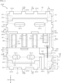
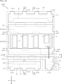
- FIG. 1 is a plan view of a semiconductor device according to a first embodiment of the present disclosure, seen through a sealing resin.
- FIG. 2 is a plan view corresponding to FIG. 1, in which the second conductive member and the third conductive member are omitted.
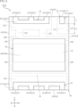
- FIG. 3 is a bottom view of the semiconductor device shown in FIG.
- FIG. 4 is a front view of the semiconductor device shown in FIG.
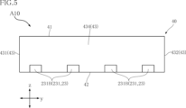
- FIG. 5 is a rear view of the semiconductor device shown in FIG.
- FIG. 6 is a right side view of the semiconductor device shown in FIG. 7 is a left side view of the semiconductor device shown in FIG.
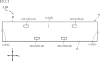
- FIG. 8 is a cross-sectional view taken along line VIII-VIII in FIG.
- FIG. 9 is a cross-sectional view taken along line IX-IX of FIG.
- FIG. 10 is a cross-sectional view taken along line XX in FIG.
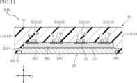
- FIG. 11 is a cross-sectional view taken along line XI-XI of FIG.
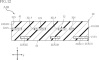
- FIG. 12 is a cross-sectional view taken along line XII-XII in FIG.
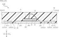
- FIG. 13 is a plan view of the semiconductor device according to the second embodiment of the present disclosure, with the sealing resin being shown through the transparent view.
- FIG. 14 is a cross-sectional view taken along line XIV-XIV in FIG.
- FIG. 15 is a cross-sectional view taken along line XV-XV in FIG.
- FIG. 16 is a plan view of the semiconductor device according to the third embodiment of the present disclosure, showing the sealing resin, the second conductive member, and the third conductive member.
- FIG. 17 is a bottom view of the semiconductor device shown in FIG. 18 is a left side view of the semiconductor device shown in FIG.
- FIG. 19 is a cross-sectional view taken along line XIX-XIX in FIG.
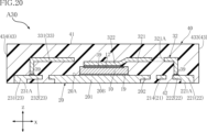
- FIG. 20 is a cross-sectional view taken along line XX-XX in FIG.
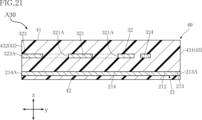
- FIG. 21 is a cross-sectional view taken along line XXI-XXI in FIG.
- a semiconductor device A10 according to a first embodiment of the present disclosure will be described with reference to FIGS. 1 to 12.
- the semiconductor device A10 is generally used in power conversion circuits such as DC-DC converters and inverters.
- the package format of the semiconductor device A10 is QFN (Quad Flat Non-leaded).
- the semiconductor device A10 includes a semiconductor element 10, a die pad 20, a first lead 21, a second lead 22, a third lead 23, a first conductive member 31, a second conductive member 32, a third conductive member 33, and a sealing resin 40.
- FIG. 1 shows the sealing resin 40 through the semiconductor device 10 for ease of understanding.
- FIG. 2 further omits the second conductive member 32 and the third conductive member 33 from FIG. 1 for ease of understanding.
- the sealing resin 40 through the sealing resin 40 is shown by an imaginary line (two-dot chain line).
- first direction z An example of a direction perpendicular to the first direction z is referred to as the "second direction x.”
- second direction x An example of a direction perpendicular to the first direction z and the second direction x is referred to as the "third direction y.”
- the sealing resin 40 covers the semiconductor element 10, the first conductive member 31, the second conductive member 32, and the third conductive member 33. Furthermore, the sealing resin 40 covers a portion of each of the die pad 20, the first lead 21, the second lead 22, and the third lead 23.
- the sealing resin 40 has electrical insulation properties.
- the sealing resin 40 is made of a material that contains, for example, black epoxy resin. As shown in Figures 4 to 8, the sealing resin 40 has a top surface 41, a bottom surface 42, and side surfaces 43.
- the top surface 41 faces the same side as the mounting surface 20A of the die pad 20, which will be described later, in the first direction z.
- the bottom surface 42 faces the opposite side to the top surface 41 in the first direction z.
- the side 43 faces in a direction perpendicular to the first direction z.
- the side 43 includes a first side 431, a second side 432, a third side 433, and a fourth side 434.
- the first side 431 and the second side 432 face opposite each other in the third direction y.
- the first side 431 and the second side 432 are located on opposite sides to each other with respect to the die pad 20.
- the third side 433 and the fourth side 434 face opposite each other in the second direction x.
- the third side 433 and the fourth side 434 are located on opposite sides to each other with respect to the die pad 20.
- the die pad 20 is located between the second lead 22 and the third lead 23 in the second direction x.
- the die pad 20 is obtained from a common lead frame together with the first lead 21, the second lead 22, and the third lead 23. Therefore, the die pad 20, the first lead 21, the second lead 22, and the third lead 23 are obtained from the same metal material.
- the die pad 20 has a mounting surface 20A, a back surface 20B, a mounting portion 201, a protruding portion 202, and a plurality of hanging portions 203.
- the mounting surface 20A and the back surface 20B face opposite each other in the first direction z.
- the mounting surface 20A faces the semiconductor element 10.
- the back surface 20B is exposed from the bottom surface 42 of the sealing resin 40.
- the mounting portion 201 includes the mounting surface 20A and the back surface 20B, and overlaps with the entire back surface 20B when viewed in the first direction z.
- the mounting portion 201 mounts the semiconductor element 10.
- the protruding portion 202 extends from the mounting portion 201 in a direction perpendicular to the first direction z.
- the protruding portion 202 includes the mounting surface 20A and is spaced apart from the bottom surface 42 of the sealing resin 40. As shown in FIG. 2, the protruding portion 202 surrounds the mounting portion 201 when viewed in the first direction z.
- the protruding portion 202 is sandwiched between the sealing resin 40 in the first direction z.
- Each of the multiple hanging portions 203 extends from the protruding portion 202 in the third direction y.
- Each of the multiple hanging portions 203 has an end surface 203A facing the third direction y. As shown in Figures 6 and 7, the end surface 203A of each of the multiple hanging portions 203 is exposed from either the first side surface 431 or the second side surface 432 of the sealing resin 40.
- the semiconductor element 10 is conductively bonded to the mounting surface 20A of the die pad 20 via a bonding layer 19.
- the bonding layer 19 is, for example, solder.
- the semiconductor element 10 is a transistor (switching element) used primarily for power conversion.
- the semiconductor element 10 is made of a material including, for example, a nitride semiconductor.
- the semiconductor element 10 is a HEMT (High Electron Mobility Transistor) made of a material including gallium nitride (GaN).
- the semiconductor element 10 has a first electrode 11, two second electrodes 12, and two third electrodes 13.
- the two third electrodes 13, the two second electrodes 12, and the first electrode 11 are located on the opposite side to the side facing the mounting surface 20A of the die pad 20 in the first direction z.
- a current corresponding to the power before being converted by the semiconductor element 10 flows through the two third electrodes 13.
- a current corresponding to the power after being converted by the semiconductor element 10 flows through the two second electrodes 12.
- a gate voltage for driving the semiconductor element 10 is applied to the first electrode 11.
- the dimension of the semiconductor element 10 in the third direction y is greater than the dimension of the semiconductor element 10 in the second direction x.
- each of the two second electrodes 12 is located next to one of the two third electrodes 13 in the third direction y.
- the first electrode 11 is located on one side of the third direction y with respect to the two second electrodes 12 in the third direction y.
- the first electrode 11 is located next to one of the two third electrodes 13 in the second direction x.
- the first lead 21 is located next to the second lead 22 in the third direction. As shown in FIG. 3, the first lead 21 is located closer to the first side surface 431 of the sealing resin 40 than to the second side surface 432 of the sealing resin 40.
- the first lead 21 has a first terminal portion 211, a first protruding portion 212, and two first hanging portions 213.
- the first terminal portion 211 has a mounting surface 211A and a side surface 211B.
- the mounting surface 211A faces the same side as the bottom surface 42 of the sealing resin 40 in the first direction z.
- the mounting surface 231A is exposed from the bottom surface 42.
- the side surface 211B faces the same side as the third side surface 433 of the sealing resin 40 in the second direction x.
- the side surface 231B is exposed from the third side surface 433.
- the first protruding portion 212 extends from the first terminal portion 211 to the side where the semiconductor element 10 is located in the second direction x.
- the first protruding portion 212 is away from the bottom surface 42.
- the first protruding portion 212 is sandwiched between the sealing resin 40 in the first direction z.
- each of the two first hanging portions 213 is connected to the first protruding portion 212.
- the two first hanging portions 213 are separated from each other in the second direction x and extend from the first protruding portion 212 in the third direction y.
- Each of the two first hanging portions 213 is sandwiched between the sealing resin 40 in the first direction z.
- Each of the two first hanging portions 213 has an end surface 213A facing the third direction y. As shown in FIGS. 6 and 12, the end surface 213A of each of the two first hanging portions 213 is exposed from the first side surface 431 of the sealing resin 40.
- the dimension L2 in the second direction x of the first protrusion 212 is greater than the dimension L1 in the second direction x of the first terminal portion 211.
- the second lead 22 is located between the first lead 21 and the second side surface 432 of the sealing resin 40 in the third direction y.
- the second lead 22 is located next to the die pad 20 in the second direction x.
- the second lead 22 has a second terminal portion 221, a second protrusion portion 222, and two connecting portions 223.
- the second terminal portion 221 has a mounting surface 221A and a plurality of side surfaces 221B.
- the mounting surface 221A faces the same side as the bottom surface 42 of the sealing resin 40 in the first direction z.
- the mounting surface 221A is exposed from the bottom surface 42.
- Each of the plurality of side surfaces 221B faces the same side as the third side surface 433 of the sealing resin 40 in the second direction x.
- Each of the plurality of side surfaces 221B is exposed from the third side surface 433.
- the second protrusion portion 222 extends from the second terminal portion 221 to the same side as the first protrusion portion 212 of the first lead 21 in the second direction x.
- the second protrusion portion 222 is away from the bottom surface 42.
- the second protrusion 222 is sandwiched between the sealing resin 40 in the first direction z.
- each of the two connecting portions 223 extends from the second protrusion 222 in the second direction x.
- the two connecting portions 223 are separated from each other in the third direction y.
- Each of the two connecting portions 223 is connected to the second protrusion 222 and the protrusion 202 of the die pad 20. Therefore, the second lead 22 is electrically connected to the die pad 20.
- Each of the two connecting portions 223 is sandwiched between the sealing resin 40 in the first direction z.
- the third lead 23 is located on the opposite side of the die pad 20 from the first lead 21 and the second lead 22 in the second direction x. As shown in FIG. 3, the third lead 23 is located closer to the fourth side surface 434 of the sealing resin 40 than to the third side surface 433 of the sealing resin 40.
- the third lead 23 has a third terminal portion 231 and a third protrusion portion 232.
- the third terminal portion 231 has a mounting surface 231A and a plurality of side surfaces 231B.
- the mounting surface 231A faces the same side as the bottom surface 42 of the sealing resin 40 in the first direction z.
- the mounting surface 231A is exposed from the bottom surface 42.
- Each of the plurality of side surfaces 231B faces the same side as the fourth side surface 434 of the sealing resin 40 in the second direction x.
- Each of the plurality of side surfaces 231B is exposed from the fourth side surface 434.
- the third protrusion portion 232 extends from the third terminal portion 231 in a direction perpendicular to the first direction z.
- the third protrusion portion 232 is separated from the bottom surface 42.
- the third protrusion portion 232 is sandwiched between the sealing resin 40 in the first direction z.
- the first conductive member 31 is conductively joined to the first electrode 11 of the semiconductor element 10 and the first protrusion 212 of the first lead 21.
- the first conductive member 31 is a wire. Therefore, the first conductive member 31 is conductively joined to the first electrode 11 and the first protrusion 212 by wire bonding.
- the first conductive member 31 extends in the second direction x.
- the first conductive member 31 is separated from the two second electrodes 12 of the semiconductor element 10 and the two third electrodes 13 of the semiconductor element 10.
- the second conductive member 32 is conductively joined to the two second electrodes 12 of the semiconductor element 10 via a bonding layer 39.
- the second conductive member 32 is a metal clip.
- the second conductive member 32 and the third conductive member 33 are obtained from a common lead frame. Therefore, the second conductive member 32 and the third conductive member 33 are obtained from the same metal material.
- the lead frame from which the second conductive member 32 is obtained is different from the lead frame from which the die pad 20 is obtained.
- the second conductive member 32 has a second base 321, two first connection portions 322, a hanging portion 323, and an arm portion 324.
- the second base 321 is located on the side where the second lead 22 is located with respect to the die pad 20 in the second direction x.
- the second base 321 is conductively joined to the second protrusion portion 222 of the second lead 22 via a bonding layer 39.
- the two second electrodes 12 of the semiconductor element 10 are electrically connected to the second lead 22.
- the second base 321 has two through holes 321A.
- the two through holes 321A are separated from each other in the third direction y. Each of the two through holes 321A penetrates the second base 321 in the first direction z.
- the two first connection portions 322 are connected to the second base portion 321.
- the two first connection portions 322 are spaced apart from each other in the third direction y.
- each of the two first connection portions 322 extends in the second direction x.
- the two first connection portions 322 are individually conductively bonded to the two second electrodes 12 of the semiconductor element 10 via a bonding layer 39.
- the hanging portion 323 and the arm portion 324 are located on opposite sides of each other in the third direction y with respect to the second base portion 321.
- the hanging portion 323 extends from the second base portion 321 in the third direction y.
- the hanging portion 323 has an end surface 323A facing the third direction y.
- the end surface 323A is exposed from the second side surface 432 of the sealing resin 40.
- the arm portion 324 includes a portion extending from the second base portion 321 in the third direction y and a portion extending from the portion in the second direction x.
- the arm portion 324 has an end surface 324A facing the second direction x. As shown in FIG. 4, the end surface 324A is exposed from the third side surface 433 of the sealing resin 40.
- the third conductive member 33 is conductively bonded to the two third electrodes 13 of the semiconductor element 10 via a bonding layer 39.
- the bonding layer 39 is, for example, solder.
- the third conductive member 33 is a metal clip.
- the third conductive member 33 has a second base 331, two second connection portions 332, and two hanging portions 333.
- the second base 331 is located on the side where the third lead 23 is located with respect to the die pad 20 in the second direction x.
- the second base 331 is conductively joined to the third protrusion 232 of the third lead 23 via a bonding layer 39.
- the two third electrodes 13 of the semiconductor element 10 are electrically connected to the third lead 23.
- the second base 331 has two through holes 331A.
- the two through holes 331A are separated from each other in the third direction y. Each of the two through holes 331A penetrates the second base 331 in the first direction z.
- the two second connection portions 332 are connected to the second base portion 331.
- the two second connection portions 332 are spaced apart from each other in the third direction y.
- each of the two second connection portions 332 extends in the second direction x.
- the two second connection portions 332 are individually conductively bonded to the two third electrodes 13 of the semiconductor element 10 via the bonding layer 39.
- each of the two hanging portions 333 extends from the second base portion 331 in the third direction y.
- the two hanging portions 333 are located on opposite sides of each other in the third direction y with respect to the second base portion 331.
- Each of the two hanging portions 333 has an end face 333A facing the third direction y. As shown in FIG. 6 and FIG. 7, the end face 333A of each of the two hanging portions 333 is individually exposed from the first side face 431 and the second side face 432 of the sealing resin 40.
- the semiconductor device A10 includes a semiconductor element 10, a first lead 21, a first conductive member 31, and a sealing resin 40.
- the first lead 21 has a first terminal portion 211 exposed from the bottom surface 42 of the sealing resin 40, a first protruding portion 212 extending from the first terminal portion 211 in the second direction x toward the side where the semiconductor element 10 is located, and a first hanging portion 213 connected to the first protruding portion 212.
- the first protruding portion 212 is separated from the bottom surface 42.
- the first hanging portion 213 is exposed from the side surface 43 of the sealing resin 40.
- the first conductive member 31 is conductively joined to the first electrode 11 of the semiconductor element 10 and the first protruding portion 212.
- the dimension L2 of the first protruding portion 212 in the second direction x is larger than the dimension L1 of the first terminal portion 211 in the second direction x.
- the length of the first conductive member 31 can be shortened.
- the first terminal portion 211 and the first hanging portion 213 can be supported by the lead frame. This reduces the deflection in the first direction z acting on the first protrusion 212 when the first conductive member 31 is conductively joined to the first protrusion 212, thereby suppressing a decrease in the reaction force in the first direction z acting from the first protrusion 212 to the first conductive member 31. Therefore, with this configuration, in the semiconductor device A10, it is possible to reduce the length of the first conductive member 31 while suppressing a decrease in the bonding strength of the first conductive member 31 to the first lead 21.
- the side 43 of the sealing resin 40 includes a first side 431 and a second side 432 that face opposite each other in the third direction y.
- the first lead 21 is located closer to the first side 431 than to the second side 432.
- the first hanging portion 213 of the first lead 21 is exposed from the first side 431.
- the semiconductor device A10 further includes a die pad 20 on which the semiconductor element 10 is mounted.
- the die pad 20 is exposed from the bottom surface 42 of the sealing resin 40. This configuration can improve the heat dissipation properties of the semiconductor device A10.
- the semiconductor device A10 further includes a second lead 22 that is electrically connected to the second electrode 12 of the semiconductor element 10.
- the second lead 22 is exposed from the bottom surface 42 of the sealing resin 40.
- the second lead 22 is located between the first lead 21 and the second side surface 432 of the sealing resin 40 in the third direction y.
- the second lead 22 is located next to the die pad 20 in the second direction x.
- the side 43 of the sealing resin 40 includes a third side 433 facing the second direction x.
- the first terminal portion 211 of the first lead 21 and the second lead 22 are exposed from the third side 433.
- FIG. 13 is seen through the sealing resin 40.
- the see-through sealing resin 40 is shown by imaginary lines.
- semiconductor device A20 the configuration of second conductive member 32 and third conductive member 33 differs from that of semiconductor device A10.
- the second conductive member 32 is a plurality of wires.
- the second conductive member 32 is conductively joined to the two second electrodes 12 of the semiconductor element 10 and the protruding portion 202 of the die pad 20 by wire bonding.
- the second conductive member 32 extends in the second direction x and is separated from the second lead 22.
- the third conductive member 33 is a plurality of wires.
- the third conductive member 33 is conductively joined to the two third electrodes 13 of the semiconductor element 10 and the third protrusion 232 of the third lead 23 by wire bonding.
- the third conductive member 33 extends in the second direction x.
- the semiconductor device A20 includes a semiconductor element 10, a first lead 21, a first conductive member 31, and a sealing resin 40.
- the first lead 21 has a first terminal portion 211 exposed from the bottom surface 42 of the sealing resin 40, a first protruding portion 212 extending from the first terminal portion 211 in the second direction x toward the side where the semiconductor element 10 is located, and a first hanging portion 213 connected to the first protruding portion 212.
- the first protruding portion 212 is spaced apart from the bottom surface 42.
- the first hanging portion 213 is exposed from the side surface 43 of the sealing resin 40.
- the first conductive member 31 is conductively joined to the first electrode 11 of the semiconductor element 10 and the first protruding portion 212.
- the dimension L2 of the first protruding portion 212 in the second direction x is greater than the dimension L1 of the first terminal portion 211 in the second direction x. Therefore, with this configuration, even in the semiconductor device A20, it is possible to reduce the length of the first conductive member 31 while suppressing a decrease in the bonding strength of the first conductive member 31 to the first lead 21. Furthermore, by having a configuration in common with the semiconductor device A10, the semiconductor device A20 achieves the same effects as the semiconductor device A10.
- the second conductive member 32 is conductively joined to the die pad 20.
- the second lead 22 is connected to the die pad 20.
- Each of the second conductive member 32 and the third conductive member 33 is a wire. This configuration allows for greater freedom in setting the conductive path length of each of the second conductive member 32 and the third conductive member 33 compared to the semiconductor device A10.
- FIG. 16 A semiconductor device A30 according to a third embodiment of the present disclosure will be described with reference to Figures 16 to 21.
- elements that are the same as or similar to those of the semiconductor device A10 described above are given the same reference numerals, and duplicated descriptions will be omitted.
- Figure 16 omits illustration of the second conductive member 32, the third conductive member 33, and the sealing resin 40.
- the first conductive member 31, the second conductive member 32, and the sealing resin 40 are each shown by imaginary lines.
- semiconductor device A30 the configuration of the first lead 21 and the second lead 22 differs from that of semiconductor device A10.
- the first lead 21 has a second suspending portion 214.
- the second suspending portion 214 is connected to the first protruding portion 212 of the first lead 21.
- the first protruding portion 212 is located between the first suspending portion 213 and the second suspending portion 214 in the third direction y.
- the second suspending portion 214 is located between the second lead 22 and the die pad 20 in the second direction x.
- the second suspending portion 214 extends in the third direction y.
- the second suspending portion 214 has an end surface 214A facing the third direction y. As shown in FIGS. 18 and 21, the end surface 214A is exposed from the second side surface 432 of the sealing resin 40.
- the second lead 22 does not have two connecting portions 223. As a result, the second lead 22 is separated from the die pad 20.
- the second base portion 321 of the second conductive member 32 is conductively joined to the second protruding portion 222 of the second lead 22 via the bonding layer 39. As shown in Figures 19 to 21, the second base portion 321 straddles the second hanging portion 214 of the second lead 22.
- the semiconductor device A30 includes a semiconductor element 10, a first lead 21, a first conductive member 31, and a sealing resin 40.
- the first lead 21 has a first terminal portion 211 exposed from the bottom surface 42 of the sealing resin 40, a first protruding portion 212 extending from the first terminal portion 211 in the second direction x toward the side where the semiconductor element 10 is located, and a first hanging portion 213 connected to the first protruding portion 212.
- the first protruding portion 212 is spaced apart from the bottom surface 42.
- the first hanging portion 213 is exposed from the side surface 43 of the sealing resin 40.
- the first conductive member 31 is conductively joined to the first electrode 11 of the semiconductor element 10 and the first protruding portion 212.
- the dimension L2 of the first protruding portion 212 in the second direction x is greater than the dimension L1 of the first terminal portion 211 in the second direction x. Therefore, with this configuration, even in the semiconductor device A30, it is possible to reduce the length of the first conductive member 31 while suppressing a decrease in the bonding strength of the first conductive member 31 to the first lead 21. Furthermore, by having a configuration common to the semiconductor device A10, the semiconductor device A30 achieves the same effects as the semiconductor device A10.
- the first lead 21 has a second suspending portion 214 that is connected to the first protruding portion 212 and is located between the second lead 22 and the die pad 20 in the second direction x.
- the second suspending portion 214 is exposed from the second side surface 432 of the sealing resin 40. This configuration allows the second suspending portion 214 to be supported by the lead frame in addition to the first terminal portion 211 and the first suspending portion 213 of the first lead 21.
- This further reduces the deflection in the first direction z acting on the first protruding portion 212 when the first conductive member 31 is conductively joined to the first protruding portion 212, thereby further suppressing the reduction in the reaction force in the first direction z acting from the first protruding portion 212 to the first conductive member 31.
- This makes it possible to more effectively suppress the reduction in the bonding strength of the first conductive member 31 to the first lead 21.
- the first protrusion 212 of the first lead 21 is located between the first suspending portion 213 and the second suspending portion 214 in the third direction y. This configuration makes it possible to more effectively reduce the deflection in the first direction z acting on the first protrusion 212. Furthermore, the dimension of the second suspending portion 214 in the direction perpendicular to the first direction z can be further shortened without the second suspending portion 214 interfering with either the second lead 22 or the die pad 20.
- Appendix 1 a semiconductor element having a first electrode located on one side in a first direction; a first lead that is spaced apart from the semiconductor element in a second direction perpendicular to the first direction and that is electrically connected to the first electrode; a first conductive member conductively connected to the first electrode and the first lead; a sealing resin that covers the semiconductor element and the first conductive member, the sealing resin has a bottom surface facing a side opposite to a side on which the first electrode is located in the first direction, and a side surface facing a direction perpendicular to the first direction, the first lead has a first terminal portion exposed from the bottom surface, a first protruding portion extending from the first terminal portion in the second direction toward a side where the semiconductor element is located and spaced from the bottom surface, and a first hanging portion connected to the first protruding portion and exposed from the side surface, the first conductive member is conductively joined to the first protruding portion, A semiconductor device, where
- the side surface includes a first side surface and a second side surface facing opposite each other in a third direction perpendicular to the first direction and the second direction, the first lead is located closer to the first side than to the second side, 2.
- the semiconductor device according to claim 1 wherein the first suspending portion is exposed from the first side surface.
- Appendix 3. A second lead is further provided in electrical communication with the second electrode.
- the semiconductor element has a second electrode located on the same side as the first electrode in the first direction, and the second lead is exposed from the bottom surface.
- Appendix 4. 4.
- the semiconductor device according to claim 3, wherein the second lead is located between the first lead and the second side surface in the third direction. Appendix 5. 5.
- Appendix 6. Further comprising a die pad on which the semiconductor element is mounted, 6. The semiconductor device according to claim 5, wherein the die pad is located adjacent to the second lead in the second direction.
- Appendix 7. 7. The semiconductor device according to claim 6, wherein the die pad is exposed from the bottom surface.
- Appendix 8. the second lead is spaced from the die pad; 8. The semiconductor device according to claim 7, wherein the second conductive member is conductively connected to the second lead.
- the first lead has a second hanging portion connected to the first protruding portion and located between the second lead and the die pad in the second direction;
- Appendix 10. The semiconductor device according to claim 9, wherein the first protrusion is located between the first suspending portion and the second suspending portion in the third direction.
- Appendix 11. The semiconductor device according to claim 10, wherein the second conductive member straddles the second hanging portion.
- the second lead has a second terminal portion exposed from the bottom surface, a second protruding portion extending from the second terminal portion to the same side as the first protruding portion in the second direction and spaced from the bottom surface, and a connecting portion connected to the second protruding portion and the die pad, 13.
- a dimension of the connecting portion in the third direction is smaller than a dimension of the second protruding portion in the third direction.
- Appendix 14. 14.
- the semiconductor device according to claim 13, wherein the second conductive member is conductively joined to the second protruding portion.
- Appendix 15. 13 The semiconductor device according to claim 12, wherein the second conductive member is conductively connected to the die pad. Appendix 16.
- the semiconductor element has a third electrode located on the same side as the first electrode in the first direction, the third lead being exposed from the bottom surface, 16.
- the side surface includes a third side surface facing the second direction, the third side surface is located on an opposite side to the third lead with respect to the die pad in the second direction, 17.
- the semiconductor device according to claim 16 wherein the first terminal portion and the second lead are exposed from the third side surface.
Landscapes
- Structures Or Materials For Encapsulating Or Coating Semiconductor Devices Or Solid State Devices (AREA)
Priority Applications (1)
| Application Number | Priority Date | Filing Date | Title |
|---|---|---|---|
| JP2024550001A JPWO2024070615A1 (https=) | 2022-09-29 | 2023-09-11 |
Applications Claiming Priority (2)
| Application Number | Priority Date | Filing Date | Title |
|---|---|---|---|
| JP2022155864 | 2022-09-29 | ||
| JP2022-155864 | 2022-09-29 |
Publications (1)
| Publication Number | Publication Date |
|---|---|
| WO2024070615A1 true WO2024070615A1 (ja) | 2024-04-04 |
Family
ID=90477520
Family Applications (1)
| Application Number | Title | Priority Date | Filing Date |
|---|---|---|---|
| PCT/JP2023/032962 Ceased WO2024070615A1 (ja) | 2022-09-29 | 2023-09-11 | 半導体装置 |
Country Status (2)
| Country | Link |
|---|---|
| JP (1) | JPWO2024070615A1 (https=) |
| WO (1) | WO2024070615A1 (https=) |
Citations (5)
| Publication number | Priority date | Publication date | Assignee | Title |
|---|---|---|---|---|
| JP2003282809A (ja) * | 2002-03-20 | 2003-10-03 | Hitachi Ltd | 半導体装置およびその製造方法 |
| JP2017028333A (ja) * | 1999-06-30 | 2017-02-02 | ルネサスエレクトロニクス株式会社 | 半導体装置の製造方法 |
| JP2021190556A (ja) * | 2020-05-29 | 2021-12-13 | ローム株式会社 | 半導体装置の実装構造 |
| WO2022138318A1 (ja) * | 2020-12-23 | 2022-06-30 | ローム株式会社 | 半導体装置の製造方法および半導体装置 |
| JP2022118383A (ja) * | 2021-02-02 | 2022-08-15 | ローム株式会社 | 半導体装置 |
-
2023
- 2023-09-11 JP JP2024550001A patent/JPWO2024070615A1/ja active Pending
- 2023-09-11 WO PCT/JP2023/032962 patent/WO2024070615A1/ja not_active Ceased
Patent Citations (5)
| Publication number | Priority date | Publication date | Assignee | Title |
|---|---|---|---|---|
| JP2017028333A (ja) * | 1999-06-30 | 2017-02-02 | ルネサスエレクトロニクス株式会社 | 半導体装置の製造方法 |
| JP2003282809A (ja) * | 2002-03-20 | 2003-10-03 | Hitachi Ltd | 半導体装置およびその製造方法 |
| JP2021190556A (ja) * | 2020-05-29 | 2021-12-13 | ローム株式会社 | 半導体装置の実装構造 |
| WO2022138318A1 (ja) * | 2020-12-23 | 2022-06-30 | ローム株式会社 | 半導体装置の製造方法および半導体装置 |
| JP2022118383A (ja) * | 2021-02-02 | 2022-08-15 | ローム株式会社 | 半導体装置 |
Also Published As
| Publication number | Publication date |
|---|---|
| JPWO2024070615A1 (https=) | 2024-04-04 |
Similar Documents
| Publication | Publication Date | Title |
|---|---|---|
| US11444010B2 (en) | Semiconductor device | |
| JP3737673B2 (ja) | 半導体装置 | |
| US8198712B2 (en) | Hermetically sealed semiconductor device module | |
| US7135761B2 (en) | Robust power semiconductor package | |
| CN101853831A (zh) | 半导体装置及其制造方法 | |
| JP7815412B2 (ja) | 半導体装置 | |
| JP2022143166A (ja) | 半導体装置 | |
| JP7594950B2 (ja) | 半導体装置 | |
| CN114068468A (zh) | 引线框架及封装结构 | |
| JP7579224B2 (ja) | 半導体装置 | |
| WO2023112677A1 (ja) | 半導体装置および半導体装置の製造方法 | |
| JP2025166256A (ja) | 半導体装置、および半導体装置の製造方法 | |
| WO2024070615A1 (ja) | 半導体装置 | |
| JP2022143167A (ja) | 半導体装置 | |
| JP7798800B2 (ja) | 半導体装置 | |
| US12166002B2 (en) | Semiconductor device including a semiconductor element having electrodes inserted into recess portions of a conductive member | |
| CN215377402U (zh) | 引线框架及封装结构 | |
| JP7278077B2 (ja) | 半導体装置およびその製造方法 | |
| US20250246534A1 (en) | Semiconductor device | |
| CN114203659A (zh) | 多层互连带 | |
| US12557667B2 (en) | Semiconductor device with lead frame having an offset portion on a die pad | |
| WO2021215472A1 (ja) | 半導体装置 | |
| JP7704594B2 (ja) | 半導体装置 | |
| WO2025158868A1 (ja) | 半導体装置 | |
| WO2025069992A1 (ja) | 半導体装置 |
Legal Events
| Date | Code | Title | Description |
|---|---|---|---|
| 121 | Ep: the epo has been informed by wipo that ep was designated in this application |
Ref document number: 23871851 Country of ref document: EP Kind code of ref document: A1 |
|
| WWE | Wipo information: entry into national phase |
Ref document number: 2024550001 Country of ref document: JP |
|
| NENP | Non-entry into the national phase |
Ref country code: DE |
|
| 122 | Ep: pct application non-entry in european phase |
Ref document number: 23871851 Country of ref document: EP Kind code of ref document: A1 |