WO2024070591A1 - 伸縮性デバイス - Google Patents
伸縮性デバイス Download PDFInfo
- Publication number
- WO2024070591A1 WO2024070591A1 PCT/JP2023/032845 JP2023032845W WO2024070591A1 WO 2024070591 A1 WO2024070591 A1 WO 2024070591A1 JP 2023032845 W JP2023032845 W JP 2023032845W WO 2024070591 A1 WO2024070591 A1 WO 2024070591A1
- Authority
- WO
- WIPO (PCT)
- Prior art keywords
- wiring
- substrate
- protective layer
- main surface
- stretchable device
- Prior art date
- Legal status (The legal status is an assumption and is not a legal conclusion. Google has not performed a legal analysis and makes no representation as to the accuracy of the status listed.)
- Ceased
Links
Images



Classifications
-
- H—ELECTRICITY
- H05—ELECTRIC TECHNIQUES NOT OTHERWISE PROVIDED FOR
- H05K—PRINTED CIRCUITS; CASINGS OR CONSTRUCTIONAL DETAILS OF ELECTRIC APPARATUS; MANUFACTURE OF ASSEMBLAGES OF ELECTRICAL COMPONENTS
- H05K1/00—Printed circuits
- H05K1/02—Details
- H05K1/0277—Bendability or stretchability details
- H05K1/0283—Stretchable printed circuits
-
- H—ELECTRICITY
- H01—ELECTRIC ELEMENTS
- H01R—ELECTRICALLY-CONDUCTIVE CONNECTIONS; STRUCTURAL ASSOCIATIONS OF A PLURALITY OF MUTUALLY-INSULATED ELECTRICAL CONNECTING ELEMENTS; COUPLING DEVICES; CURRENT COLLECTORS
- H01R12/00—Structural associations of a plurality of mutually-insulated electrical connecting elements, specially adapted for printed circuits, e.g. printed circuit boards [PCB], flat or ribbon cables, or like generally planar structures, e.g. terminal strips, terminal blocks; Coupling devices specially adapted for printed circuits, flat or ribbon cables, or like generally planar structures; Terminals specially adapted for contact with, or insertion into, printed circuits, flat or ribbon cables, or like generally planar structures
- H01R12/50—Fixed connections
- H01R12/59—Fixed connections for flexible printed circuits, flat or ribbon cables or like structures
- H01R12/61—Fixed connections for flexible printed circuits, flat or ribbon cables or like structures connecting to flexible printed circuits, flat or ribbon cables or like structures
-
- H—ELECTRICITY
- H05—ELECTRIC TECHNIQUES NOT OTHERWISE PROVIDED FOR
- H05K—PRINTED CIRCUITS; CASINGS OR CONSTRUCTIONAL DETAILS OF ELECTRIC APPARATUS; MANUFACTURE OF ASSEMBLAGES OF ELECTRICAL COMPONENTS
- H05K1/00—Printed circuits
- H05K1/02—Details
- H05K1/14—Structural association of two or more printed circuits
-
- H—ELECTRICITY
- H05—ELECTRIC TECHNIQUES NOT OTHERWISE PROVIDED FOR
- H05K—PRINTED CIRCUITS; CASINGS OR CONSTRUCTIONAL DETAILS OF ELECTRIC APPARATUS; MANUFACTURE OF ASSEMBLAGES OF ELECTRICAL COMPONENTS
- H05K1/00—Printed circuits
- H05K1/02—Details
- H05K1/14—Structural association of two or more printed circuits
- H05K1/142—Arrangements of planar printed circuit boards in the same plane, e.g. auxiliary printed circuit insert mounted in a main printed circuit
-
- H—ELECTRICITY
- H05—ELECTRIC TECHNIQUES NOT OTHERWISE PROVIDED FOR
- H05K—PRINTED CIRCUITS; CASINGS OR CONSTRUCTIONAL DETAILS OF ELECTRIC APPARATUS; MANUFACTURE OF ASSEMBLAGES OF ELECTRICAL COMPONENTS
- H05K3/00—Apparatus or processes for manufacturing printed circuits
- H05K3/36—Assembling printed circuits with other printed circuits
-
- H—ELECTRICITY
- H05—ELECTRIC TECHNIQUES NOT OTHERWISE PROVIDED FOR
- H05K—PRINTED CIRCUITS; CASINGS OR CONSTRUCTIONAL DETAILS OF ELECTRIC APPARATUS; MANUFACTURE OF ASSEMBLAGES OF ELECTRICAL COMPONENTS
- H05K2201/00—Indexing scheme relating to printed circuits covered by H05K1/00
- H05K2201/05—Flexible printed circuits [FPCs]
- H05K2201/058—Direct connection between two or more FPCs or between flexible parts of rigid PCBs
-
- H—ELECTRICITY
- H05—ELECTRIC TECHNIQUES NOT OTHERWISE PROVIDED FOR
- H05K—PRINTED CIRCUITS; CASINGS OR CONSTRUCTIONAL DETAILS OF ELECTRIC APPARATUS; MANUFACTURE OF ASSEMBLAGES OF ELECTRICAL COMPONENTS
- H05K2201/00—Indexing scheme relating to printed circuits covered by H05K1/00
- H05K2201/07—Electric details
- H05K2201/0753—Insulation
-
- H—ELECTRICITY
- H05—ELECTRIC TECHNIQUES NOT OTHERWISE PROVIDED FOR
- H05K—PRINTED CIRCUITS; CASINGS OR CONSTRUCTIONAL DETAILS OF ELECTRIC APPARATUS; MANUFACTURE OF ASSEMBLAGES OF ELECTRICAL COMPONENTS
- H05K2201/00—Indexing scheme relating to printed circuits covered by H05K1/00
- H05K2201/09—Shape and layout
- H05K2201/09209—Shape and layout details of conductors
- H05K2201/09218—Conductive traces
- H05K2201/09236—Parallel layout
Definitions
- This disclosure relates to stretchable devices.
- a conventional stretchable device is described in JP 2008-108890 A (Patent Document 1).
- This stretchable device has a first substrate, a first wiring provided on the first substrate, a second substrate facing the first substrate in the thickness direction of the first substrate, a second wiring provided on the second substrate facing the first wiring in the thickness direction, and a connection member that electrically connects the first wiring and the second wiring.
- the region where the first wiring and the second wiring overlap and the region where the connection member exists constitute a wiring region where the first wiring and the second wiring are electrically connected.
- the wiring region coincides with the substrate overlap region where the first substrate and the second substrate overlap.
- the protective layer is provided on all parts of the first wiring that are exposed from the second substrate. In other words, when viewed from the thickness direction, the wiring region where the first wiring and the second wiring are electrically connected and the protective layer overlap region where the first substrate and the protective layer overlap are adjacent to each other.
- the object of the present disclosure is to provide a stretchable device that can reduce damage to the stretchable device when stretching the device and can also suppress deterioration of the performance of the stretchable device.
- a stretchable device includes: A first base material having elasticity; A first wiring provided on a first main surface of the first base material; a second base material that faces the first base material in a first direction that is a thickness direction of the first base material and is connected to the first base material; a second wiring provided on a first main surface of the second base material, facing the first wiring in the first direction, and electrically connected to the first wiring; a first protective layer provided on the first main surface of the first base material so as to cover a portion of the first wiring; A first overlap region where the first base material and the first protective layer overlap as viewed from the first direction is separated from a wiring region where the first wiring and the second wiring are electrically connected.
- the stretchable device can reduce damage to the stretchable device when stretching the device, and can also suppress deterioration of the performance of the stretchable device.
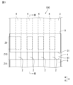
- FIG. 1 is a partially enlarged top view diagrammatically illustrating a stretchable device according to a first embodiment of the present disclosure.
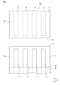
- FIG. 2 is an exploded plan view illustrating a schematic diagram of the stretchable device according to the first embodiment of the present disclosure.
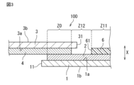
- FIG. 3 is a cross-sectional view taken along line III-III of FIG.
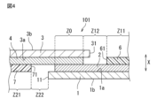
- FIG. 4 is a partial cross-sectional view of a stretchable device according to a second embodiment of the present disclosure.
- FIG. 5 is a partial cross-sectional view of a stretchable device according to a third embodiment of the present disclosure.
- FIG. 6 is a partial cross-sectional view of a stretchable device according to a fourth embodiment of the present disclosure.
- FIG. 1 is a partially enlarged top view diagrammatically illustrating a stretchable device according to a first embodiment of the present disclosure.
- FIG. 2 is an exploded plan view illustrating a schematic diagram of the stretchable device according to the first embodiment of the present disclosure.
- FIG. 3 is a cross
- FIG. 7 is a partial cross-sectional view of a stretchable device according to a fifth embodiment of the present disclosure.
- FIG. 8 is a partial cross-sectional view of a stretchable device according to a sixth embodiment of the present disclosure.
- FIG. 9 is a partial cross-sectional view of a stretchable device according to a seventh embodiment of the present disclosure.
- FIG. 10 is a partial cross-sectional view of a stretchable device according to an eighth embodiment of the present disclosure.
- Fig. 1 is a partial top view of the stretchable device 100.
- Fig. 2 is an exploded plan view of the stretchable device 100.
- Fig. 3 is a cross-sectional view of the stretchable device 100 taken along line III-III in Fig. 1. Note that the cross-sectional views in this specification are cross-sectional views parallel to the first direction, including an area where the first substrate 1 and the second substrate 3 overlap, as viewed from a first direction, which is the thickness direction of the first substrate.
- the first direction is indicated by a double-headed arrow X.
- the thickness direction of the first substrate 1, the thickness direction of the second substrate 3, and the first direction X coincide with each other.
- the stretchable device 100 comprises a first substrate 1, a second substrate 3, a first wiring 2, a second wiring 4, and a first protective layer 6.
- the first substrate 1 and the second substrate 3 are connected.
- the first wiring 2 provided on the first main surface 1a of the first substrate 1 and the second wiring 4 provided on the first main surface 3a of the second substrate 3 are electrically connected.
- the first protective layer 6 is provided on the first main surface 1a of the first substrate 1 so as to cover a portion of the first wiring 2.
- the shape of the stretchable device 100 is not particularly limited. In this specification, a structure in which two substrates are connected is described as an example, but three or more substrates may be connected.
- the first wiring 2 is not limited to the arrangement shown in FIG. 1, and the extension direction is not limited either. Specifically, the longitudinal direction of the first substrate 1 and the extension direction of the first wiring 2 do not have to coincide, and the first wiring 2 does not have to extend in one direction.
- the number of first wirings 2 is not particularly limited, and may be one or more. When there are multiple first wirings 2, they may include wiring that is not electrically connected to the second wiring 4. The same applies to the arrangement and number of second wirings 4.
- “above” in this specification does not have to coincide with the top and bottom when the stretchable device 100 is in use. More specifically, “on the main surface of the first substrate 1" does not refer to an absolute direction such as vertically upward as determined by the direction of gravity, but rather refers to the direction toward the outside of the outside and inside that are bounded by the main surface of the first substrate 1. The same is true for “on the main surface of the second substrate 3.”
- “above” with respect to an element includes not only an upper position away from the element, that is, an upper position via another object on the element or an upper position with a gap therebetween, but also a position directly above the element (on).
- first substrate 1 and the second substrate 3 face each other in the first direction X, and partially overlap when viewed from the first direction X.
- first wiring 2 and the second wiring 4 face each other in the first direction X.
- the first substrate 1 is stretchable. By having the first substrate 1 stretchable, the stretching of the first wiring 2 is not inhibited, and the risk of breakage due to stretching during use of the stretchable device 100 can be reduced.
- a stretchable substrate is a sheet- or film-shaped substrate made of a stretchable resin material.
- the resin material preferably contains at least one resin selected from the group consisting of acrylic resins, styrene resins, and urethane resins.
- An example of an urethane resin is thermoplastic polyurethane.
- the thickness of the first substrate 1 is not particularly limited, but from the viewpoint of not inhibiting the stretching of the surface of the living body when attached to the living body, it is preferably 1 mm or less, more preferably 100 ⁇ m or less, and even more preferably 50 ⁇ m or less. In addition, the thickness of the first substrate 1 is more preferably 1 ⁇ m or more.
- the first substrate 1 has a first main surface 1a and a second main surface 1b located opposite each other.
- the first substrate 1 has a first substrate end 11 connecting the first main surface 1a and the second main surface 1b.
- the first substrate end 11 is the end of the first substrate 1 that is closer to the second substrate 3, in other words, the end that overlaps with the second wiring 4 when viewed from the first direction X.
- ends different from the first substrate end 11 are not shown in FIGS. 1, 2, and 3.
- the first wiring 2 is provided on the first main surface 1a of the first substrate 1.
- the first wiring 2 is preferably elastic.
- materials for the first wiring 2 include a mixture of metal powder such as Ag, Cu, and/or Ni as conductive particles and an elastomer resin such as a silicone resin.
- the average particle size of the conductive particles is not particularly limited, but is preferably 0.01 ⁇ m or more and 10 ⁇ m or less.
- the conductive particles are preferably spherical in shape, and may be flat or have a protruding structure to improve elasticity.
- the elastomer resin contains at least one resin (elastomer resin) selected from the group consisting of epoxy resin, urethane resin, acrylic resin, and silicone resin, which is preferable for ensuring elasticity.
- the thickness of the first wiring 2 is preferably 100 ⁇ m or less, and more preferably 50 ⁇ m or less.
- the thickness of the elastic wiring is more preferably 1 ⁇ m or more.
- the thickness, width, and length of the first wiring are not particularly limited.
- the first wiring 2 does not have to be elastic.
- the material of the first wiring 2 is, for example, a conductive paste containing a mixture of Ag and resin
- the conductive paste is applied to the first substrate 1.
- the application method may be screen printing, gravure printing, or inkjet printing.
- the conductive paste is then thermally cured to obtain a predetermined resistance value, thereby forming the first wiring 2 on the first substrate 1.
- the second substrate 3 is preferably elastic.
- the second substrate 3 preferably has a larger Young's modulus than the first wiring 2.
- Specific examples include substrates such as FPC (Flexible Printed Circuit), FFC (Flexible Flat Cable), and PCB (Printed Circuit Board).
- FPC Flexible Printed Circuit
- FFC Flexible Flat Cable
- PCB Printed Circuit Board
- the second substrate 3 has a first main surface 3a and a second main surface 3b located opposite each other.
- the second substrate 3 has a second substrate end 31 connecting the first main surface 3a and the second main surface 3b.
- the second substrate end 31 is the end of the second substrate 3 closer to the first substrate 1, in other words, the end that overlaps with the first wiring 2 when viewed from the first direction X. Specifically, of both ends in the up-down direction in FIG. 1, it is the end closer to the first substrate 1, and of both ends in the left-right direction in FIG. 3, it is the end closer to the first substrate 1. Note that ends different from the second substrate end 31 are not shown in FIGS. 1, 2, and 3.
- the second substrate 3 is connected to the first substrate 1. That is, the first main surface 1a of the first substrate 1 and the first main surface 3a of the second substrate 3 are directly connected by welding or the like. Specifically, the first main surface 1a of the first substrate 1 and the first main surface 3a of the second substrate 3 are thermocompression bonded.
- the first substrate 1 and the second substrate 3 may be connected via an adhesive member such as a thermoplastic adhesive.
- the second substrate 3 does not have to be stretchable.
- materials for the second substrate 3 include sheet- or film-shaped substrates such as PET and polyimide, and substrates such as FPC, FFC, and PCB.
- the material for the second substrate 3 may be the same as the material for the first substrate 1.
- the second wiring 4 is provided on the first main surface 3a of the second substrate 3.
- the second wiring 4 is preferably elastic.
- the second wiring 4 is preferably a wiring having a larger Young's modulus than the first wiring 2.
- a metal wiring such as copper foil can be used.
- the thickness of the second wiring 4 is preferably 1 ⁇ m or more and 100 ⁇ m or less, and more preferably 50 ⁇ m or less.
- the first wiring 2 and the second wiring 4 are in direct contact with each other and electrically connected.
- the second wiring 4 does not have to be elastic.
- the material of the second wiring 4 may be the same as the material of the first wiring 2.
- the second wiring 4 is electrically connected to the first wiring 2. Specifically, the first wiring 2 and the second wiring 4 are in contact with each other and electrically connected to each other. When viewed from the first direction X, a region where the first wiring 2 and the second wiring 4 overlap constitutes a wiring region Z0 where the first wiring 2 and the second wiring 4 are electrically connected to each other.
- the first wiring 2 and the second wiring 4 may be electrically connected via a conductive connecting member. In this case, when viewed from the first direction X, the region where the first wiring 2 and the second wiring 4 overlap and the region where the connecting member exists configure a wiring region Z0 where the first wiring 2 and the second wiring 4 are electrically connected.
- the first protective layer 6 is provided on the first main surface 1a of the first substrate 1 so as to cover a portion of the first wiring 2. In this way, the first protective layer 6 covers a portion of the first wiring 2, so that even if water droplets or foreign matter adhere across the gap between adjacent first wirings 2, it is possible to suppress short circuits between adjacent first wirings 2, and it is also possible to suppress the first wirings 2 from coming into contact with air or moisture, thereby suppressing the occurrence of oxidation or corrosion of the first wirings 2.
- the first protective layer 6 may be provided so as to cover all of the first wirings 2 as a whole, or the first protective layer 6 may be provided in separate portions so as to cover each of the first wirings 2 individually.
- the first protective layer 6 covers a portion of the first wiring 2, contacts the first main surface 1a of the first substrate 1, and overlaps with the first substrate 1 when viewed from the first direction X.
- the first protective layer 6 contacts a portion of the area of the first substrate 1 that is exposed from the first wiring 2. Note that the first protective layer 6 does not have to cover the first wiring 2 and not contact the first substrate 1.
- the first protective layer 6 are preferably a resin material or a mixture of a resin material and an inorganic material.
- the resin material include urethane-based, styrene-based, olefin-based, silicone-based, fluorine-based, nitrile rubber, latex rubber, vinyl chloride, ester-based, amide-based, and other elastomer-based resins, epoxy, phenolic, acrylic, polyester, imide-based, rosin, cellulose, polyethylene terephthalate-based, polyethylene naphthalate-based, and polycarbonate-based resins.
- the first protective layer 6 is preferably insulating. By making the first protective layer 6 insulating, ion migration of the first wiring 6 can be more reliably suppressed.
- the first protective layer 6 is provided, for example, by applying an insulating material or attaching a laminate material.
- the thickness of the first protective layer 6 is preferably 1 ⁇ m or more and 100 ⁇ m or less, and more preferably 50 ⁇ m or less. By making the thickness of the first protective layer 6 1 ⁇ m or more, the durability of the first protective layer 6 can be ensured. Furthermore, by making the thickness of the first protective layer 6 100 ⁇ m or less, the overall height can be reduced. Note that if the thickness of the first protective layer 6 is not constant, the maximum dimension of the first protective layer 6 in the first direction X is taken as the thickness.
- the first protective layer 6 also has a first protective layer end 61.
- the first protective layer end 61 is the end of the first protective layer 6 that is closer to the first substrate end 11, specifically, of both ends in the up-down direction in FIG. 1, it is the end that is closer to the first substrate end 11, and of both ends in the left-right direction in FIG. 3, it is the end that is closer to the first substrate end 11. Note that ends different from the first protective layer end 61 are not shown in FIGS. 1, 2, and 3.
- the first overlap region Z11 where the first substrate 1 and the first protective layer 6 overlap is separated from the wiring region Z0 where the first wiring 2 and the second wiring 4 are electrically connected.
- the first protective layer end 61 and the end of the second wiring 4 are separated.
- the wiring region Z0 and the first overlap region Z11 are separated in the extension direction of the first wiring 2.
- the extension direction of the first wiring 2 and the extension direction of the second wiring 4 are the same.
- the first overlap region Z11 is separated from the wiring region Z0 when viewed from the first direction X, so that a first non-overlapping region Z12 that does not overlap with the first protective layer 6 of the first substrate 1 exists between the first overlap region Z11 and the wiring region Z0 when viewed from the first direction X.
- the first non-overlapping region Z12 exists between the first protective layer end 61 and the end of the second wiring 4 when viewed from the first direction X.
- the stress applied to the stretchable device 100 can be alleviated in the first non-overlapping region Z12. This makes it possible to reduce damage to the stretchable device 100, such as breakage of the first wiring 2, and also to suppress deterioration in the performance of the stretchable device 100, such as an increase in the resistance value of the first wiring 2.
- the stretchability of the first substrate 1 decreases, and this becomes a portion with high rigidity in the stretchable device 100.
- the first overlapping region Z11 the first substrate 1, the first wiring 2, and the first protective layer 6 overlap, so the stretchability of the first substrate 1 decreases, and this becomes a portion with high rigidity in the stretchable device 100.
- the first non-overlapping region Z12 the first substrate 1 is not covered with the first protective layer 6, so the stretchability of the first substrate 1 can be ensured, and this becomes a portion with stretchability in the stretchable device 100. Therefore, when the stretchable device 100 stretches or shrinks, the stress applied to the portion with high rigidity can be absorbed by the first non-overlapping region Z12.
- the inventor of the present application focused on the fact that when the stretchable device 100 is stretched, stress is concentrated locally in a portion with high rigidity. Furthermore, the inventor of the present application focused on the fact that the rigidity of the wiring region Z0 is different from that of the first overlapping region Z11 because the number of layers in the wiring region Z0 (four layers: the first wiring 2, the second wiring 4, the first substrate 1, and the second substrate 3) is different from the number of layers in the first overlapping region Z11 (three layers: the first substrate 1, the first wiring 2, and the first protective layer 6).
- the inventor of the present application found that when the wiring region Z0 and the first overlapping region Z11 are adjacent to each other as viewed from the first direction X as in the conventional case, stress is concentrated between the wiring region Z0 and the first overlapping region Z11. From this perspective, the inventor of the present application has realized a stretchable device 100 that can relieve stress by making the portion where this stress is concentrated (i.e., between the wiring region Z0 and the first overlapping region Z11) a stretchable portion (i.e., the first non-overlapping region Z12).
- the shortest distance between the first overlap region Z11 and the wiring region Z0 as viewed from the first direction X is 1 ⁇ m or more and 30 mm or less, more preferably 1 ⁇ m or more and 10 mm or less.
- the shortest distance between the first protective layer end 61 and the second substrate end 31 in the extension direction of the first wiring 2 is 1 ⁇ m or more and 30 mm or less. Therefore, since the shortest distance is 1 ⁇ m or more, the expansion and contraction performance of the first substrate 1 can be improved in the first non-overlapping region Z12, and stress relaxation can be improved in the first non-overlapping region Z12.
- the shortest distance is 30 mm or less, the expansion and contraction performance of the first substrate 1 can be sufficiently ensured in the first non-overlapping region Z12, and exposure of the first wiring 2 can be reduced to reduce short circuits between adjacent first wirings 2.
- connection in the stretchable device 100 will be described.
- the first substrate 1 and the second substrate 3 are thermocompression-bonded by applying heat and pressure. This connects the first substrate 1 and the second substrate 3.
- the first wiring 2 and the second wiring 4 are in contact with each other and electrically connected.
- Fig. 4 is a partial cross-sectional view of a stretchable device 101 according to the second embodiment.
- the stretchable device 101 according to the second embodiment is different from the stretchable device 100 according to the first embodiment in that a second protective layer is provided.
- the stretchable device 101 of the second embodiment further includes a second protective layer 7.
- the material and thickness of the second protective layer 7 are the same as the material and thickness of the first protective layer 6, but the thickness may be different, and similarly the material may be different.
- the second protective layer 7 is provided on the first main surface 3a of the second substrate 3 so as to cover a portion of the second wiring 4. In this way, the second protective layer 7 covers a portion of the second wiring 4, so that even if water droplets or foreign matter adhere across the gap between adjacent second wirings 4, it is possible to suppress short circuits between adjacent second wirings 4, and it is also possible to suppress the exposure of the second wiring 4 to air and moisture, thereby suppressing the occurrence of oxidation and corrosion of the second wiring 4.
- the second protective layer 7 covers a portion of the second wiring 4, contacts the first main surface 3a of the second substrate 3, and overlaps with the second substrate 3 when viewed from the first direction X.
- the second protective layer 7 contacts a portion of the area of the second substrate 3 that is exposed from the second wiring 4. Note that the second protective layer 7 does not have to cover the second wiring 4 and not contact the second substrate 3.
- the second protective layer 7 has a second protective layer end 71.
- the second protective layer end 71 is the end of the second protective layer 7 that is closer to the second substrate end 31, specifically, of both ends in the left-right direction in FIG. 4, it is the end that is closer to the second substrate end 31. Note that ends different from the second protective layer end 71 are not shown in FIG. 4.
- the second overlap region Z21 where the second substrate 3 and the second protective layer 7 overlap is separated from the wiring region Z0.
- the second protective layer end 71 and the first substrate end 11 are separated.
- the wiring region Z0 and the second overlap region Z21 are separated in the extension direction of the second wiring 4.
- the extension direction of the first wiring 2 and the extension direction of the second wiring 4 are the same.
- the second overlap region Z21 is separated from the wiring region Z0 when viewed from the first direction X, so that a second non-overlapping region Z22 that does not overlap with the second protective layer 7 of the second substrate 3 exists between the second overlap region Z21 and the wiring region Z0 when viewed from the first direction X.
- the second non-overlapping region Z22 exists between the second protective layer end 71 and the first substrate end 11 when viewed from the first direction X.
- the stretchable device 101 when the stretchable device 101 is stretched, the stress applied to the stretchable device 101 can be alleviated in the second non-overlapping region Z22.
- damage to the stretchable device 101 such as breakage of the second wiring 4 can be reduced, and a decrease in the performance of the stretchable device 101, such as an increase in the resistance value of the second wiring 4, can be suppressed.
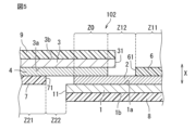
- Fig. 5 is a partial cross-sectional view of a stretchable device 102 according to the third embodiment.
- the stretchable device 102 according to the third embodiment is different from the stretchable device 101 according to the second embodiment in that a third protective layer and a fourth protective layer are provided.
- the stretchable device 102 of the third embodiment further includes a third protective layer 8 and a fourth protective layer 9.
- the material and thickness of the third protective layer 8 and the fourth protective layer 9 are the same as the material and thickness of the first protective layer 6, but the thickness may be different, and similarly the material may be different.
- the third protective layer 8 is provided on the second main surface 1b of the first substrate 1.
- the third protective layer 8 preferably covers the entire second main surface 1b of the first substrate 1, but it is sufficient if it covers at least a portion of the second main surface 1b of the first substrate 1.
- the third protective layer 8 improves the waterproof performance of the first substrate 1. Furthermore, by using a biocompatible material for the third protective layer 8, biocompatibility is improved.
- the fourth protective layer 9 is provided on the second main surface 3b of the second substrate 3.
- the fourth protective layer 9 preferably covers the entire second main surface 3b of the second substrate 3, but may cover only a portion of the second main surface 3b of the second substrate 3.
- the fourth protective layer 9 improves the waterproof performance of the second substrate 3. Furthermore, by using a biocompatible material for the fourth protective layer 9, biocompatibility is improved.
- the third protective layer 8 and the fourth protective layer 9 may be provided. Also, at least one of the third protective layer 8 and the fourth protective layer 9 may be provided for the stretchable device 100 according to the first embodiment.
- Fig. 6 is a partial cross-sectional view of a stretchable device 103 according to the fourth embodiment.
- the stretchable device 103 according to the fourth embodiment is different from the stretchable device 100 according to the first embodiment in that a first insulating layer and a second insulating layer are provided.
- the stretchable device 103 of the fourth embodiment further includes a first insulating layer 21 and a second insulating layer 22.
- the material of the first insulating layer 21 and the second insulating layer 22 is different from the material of the first protective layer 6.
- the first insulating layer 21 and the second insulating layer 22 are preferably made of a material that has a lower water absorption rate than the first substrate 1.
- materials for the first insulating layer 21 and the second insulating layer 22 include silicone resins, acrylic resins, olefin resins, modified urethane resins, vinyl chloride resins, polyester resins, polyamide resins, polyolefin resins, polyethylene resins, and polypropylene resins.
- the first insulating layer 21 and the second insulating layer 22 are formed, for example, by printing.
- the first insulating layer 21 covers at least a part of the exposed surface of the first wiring 2.
- the exposed surface of the first wiring 2 is the surface of the outer surface of the first wiring 2 that is exposed to the outside. Specifically, the exposed surface of the first wiring 2 is the surface of the first wiring 2 that is not covered by the first substrate 1, the first protective layer 6, and the second wiring 4.
- the first insulating layer 21 preferably covers the entire exposed surface of the first wiring 2, but may cover a part of the exposed surface of the first wiring 2.
- the first insulating layer 21 is also preferably present between the first wiring 2 and the first protective layer 6.
- the first insulating layer 21 does not overlap the second wiring 4 in the first direction X, but a part of the first insulating layer 21 may overlap the second wiring 4 in the first direction X. According to the above configuration, the first insulating layer 21 prevents a short circuit between adjacent first wirings 2 due to water droplets or foreign matter, improving reliability.
- An insulating paste which is the material of the first insulating layer 21, is printed on the first wiring 2 using a screen printing method or the like. At this time, in a cross section perpendicular to the extension direction of the first wiring 2, the insulating paste is preferably printed to a size 1 ⁇ m to 10 mm larger than the width of the first wiring 2, and more preferably 20 ⁇ m to 1000 ⁇ m larger.
- the second insulating layer 22 covers at least a part of the exposed surface of the second wiring 4.
- the exposed surface of the second wiring 4 is the surface of the outer surface of the second wiring 4 that is exposed to the outside.
- the exposed surface of the second wiring 4 is the surface of the second wiring 4 that is not covered by the second substrate 3 and the first wiring 2.
- the second insulating layer 22 preferably covers the entire exposed surface of the second wiring 4, but may cover a part of the exposed surface of the second wiring 4.
- the second insulating layer 22 does not overlap the first wiring 2 in the first direction X, but a part of the second insulating layer 22 may overlap the first wiring 2 in the first direction X. According to the above configuration, the second insulating layer 22 prevents short circuits between adjacent second wirings 4 due to water droplets or foreign matter, improving reliability.
- first insulating layer 21 and the second insulating layer 22 may be provided for the stretchable devices 101 and 102 according to the second and third embodiments.
- Fig. 7 is a partial cross-sectional view of a stretchable device 104 according to the fifth embodiment.
- the stretchable device 104 according to the fifth embodiment is different from the stretchable device 103 according to the fourth embodiment in that a third insulating layer and a fourth insulating layer are provided.
- the stretchable device 104 of the fifth embodiment further includes a third insulating layer 23 and a fourth insulating layer 24.
- the materials of the third insulating layer 23 and the fourth insulating layer 24 may be the same as the materials of the first insulating layer 21 and the second insulating layer 22, or may be different materials.
- the third insulating layer 23 is disposed between the first wiring 2 and the first substrate 1 in the first direction X.
- the third insulating layer 23 is provided on the first main surface 1a of the first substrate 1, and is in contact with the lower surface of the first wiring 2 (i.e., the surface of the first wiring 2 facing the first main surface 1a of the first substrate 1).
- first substrate 1 is moisture permeable, moisture may penetrate from the first substrate 1 to the first wiring 2, causing ion migration.
- the third insulating layer 23 it is possible to prevent moisture from penetrating from the first substrate 1 to the first wiring 2.
- a stretchable device 104 is provided that prevents short circuits in the first wiring 2.
- the fourth insulating layer 24 is disposed between the second wiring 4 and the second substrate 3 in the first direction X.
- the fourth insulating layer 24 is provided on the first main surface 3a of the second substrate 3 and is in contact with the lower surface of the second wiring 4 (i.e., the surface of the second wiring 4 facing the first main surface 3a of the second substrate 3).
- the second substrate 3 is moisture permeable, moisture may penetrate from the second substrate 3 to the second wiring 4, causing ion migration.
- the fourth insulating layer 24 it is possible to suppress the penetration of moisture from the second substrate 3 to the second wiring 4.
- a stretchable device 104 is provided that suppresses short circuits in the second wiring 4.
- the third insulating layer 23 and the fourth insulating layer 24 may be provided for the stretchable devices 100, 101, and 102 according to the first, second, and third embodiments.
- the third insulating layer 23 may be arranged, for example, so as to cover only the underside of the first wiring 2, or may be arranged in a portion of the first substrate 1 where there is no first wiring 2.
- the third insulating layer 23 may be arranged so as to cover the entire first substrate 1. As long as the third insulating layer 23 is in contact with the second wiring 2, a different layer may be arranged between the first substrate 1 and the third insulating layer 23.
- the fourth insulating layer 24 may be similar to the third insulating layer 23.
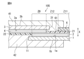
- Fig. 8 is a partial cross-sectional view of a stretchable device 105 according to the sixth embodiment.
- the stretchable device 105 according to the sixth embodiment is different from the stretchable device 103 according to the fourth embodiment in that a first covering layer and a second covering layer are provided.
- the stretchable device 105 of the sixth embodiment further includes a first covering layer 41 and a second covering layer 42.
- the materials of the first covering layer 41 and the second covering layer 42 are different from the material of the first protective layer 6.
- the first covering layer 41 covers at least the end of the second substrate 3 on the first substrate side. With this structure, the second substrate 3 can be protected from external forces. More preferably, the first covering layer 41 covers the first main surface 1a side of the first substrate 1. Specifically, the first covering layer 41 covers at least a portion of the first main surface 1a of the first substrate 1, at least a portion of the first insulating layer 21, at least a portion of the first protective layer 6, and at least a portion of the second main surface 3b of the second substrate 3. With this structure, the portion of the first wiring 2 exposed from the first protective layer 6 and the first protective layer 6 can be protected from external forces.
- the first coating layer 41 is a resin material.
- the first coating layer 41 is preferably a resin having flexibility. Specifically, it may be formed of ionomer resin, polyester resin, styrene resin, olefin resin, epoxy resin, urethane resin, acrylic resin, or silicone resin, and is preferably formed of silicone resin.
- the first coating layer 41 may also be a thermoplastic resin. Specifically, it may be thermoplastic polyurethane (TPU), or styrene-butadiene-styrene copolymer resin (SBS) as a styrene resin.
- TPU thermoplastic polyurethane
- SBS styrene-butadiene-styrene copolymer resin
- the first coating layer 41 may be composed of multiple members. By using a resin for the first coating layer 41, the connection part can be more effectively protected from external forces.
- the second covering layer 42 covers at least the end of the first substrate 1 on the second substrate side. With this structure, the first substrate 1 can be protected from external forces. More preferably, the second covering layer 42 covers the first main surface 3a side of the second substrate 3. Specifically, the second covering layer 42 covers at least a portion of the first main surface 3a of the second substrate 3, at least a portion of the second insulating layer 22, and at least a portion of the second main surface 1b of the first substrate 1. With the above-mentioned configuration, the portion of the second wiring 4 exposed from the second insulating layer 22 and the second insulating layer 22 can be protected from external forces.
- the second coating layer 42 is a resin material.
- the first coating layer 41 is preferably a resin having flexibility. Specifically, it may be formed of ionomer resin, polyester resin, styrene resin, olefin resin, epoxy resin, urethane resin, acrylic resin, or silicone resin, and is preferably formed of silicone resin.
- the second coating layer 42 may also be a thermoplastic resin. Specifically, it may be thermoplastic polyurethane (TPU), or styrene-butadiene-styrene copolymer resin (SBS) as a styrene resin.
- TPU thermoplastic polyurethane
- SBS styrene-butadiene-styrene copolymer resin
- the second coating layer 42 may be composed of a plurality of members. By using a resin for the second coating layer 42, the connection portion can be more suitably protected from external forces.
- the first coating layer 41 and the second coating layer 42 may be the same member or different
- Members containing resin such as the first protective layer 6, the first insulating layer 21, and the second insulating layer 22, may have cytotoxicity.
- the first coating layer 41 it is possible to suppress leakage of cytotoxic components.
- the same effect can be achieved for the second coating layer 42.
- the first coating layer 41 and the second coating layer 42 it is possible to further suppress leakage of cytotoxic components.
- the first covering layer 41 continuously covers the second main surface 3b of the second substrate 3, the first insulating layer 21, and the first protective layer 6.
- the first covering layer 41 continuously covers the wiring region Z0, the first non-overlapping region Z12, and the first overlapping region Z11.
- the first covering layer 41 covers the first non-overlapping region Z12 that forms a recess with respect to the wiring region Z0 and the first overlapping region Z11, so a stretchable device 105 that can reduce the recess can be provided. Therefore, a stretchable device 105 with improved wearability can be provided.
- the first covering layer 41 overlaps the first protective layer 6 when viewed from the first direction X.
- the first covering layer 41 is disposed on the first protective layer 6, and the step between the first main surface 1a side of the first substrate 1 and the second main surface 3b side of the second substrate 3 is reduced by the thickness of the first protective layer 6.
- the second coating layer 42 also continuously covers the first main surface 3a of the second substrate 3 and the second main surface 1b of the first substrate 1. This makes it possible to prevent damage to the first main surface 3a of the second substrate 3 and the second main surface 1b of the first substrate 1.
- first covering layer 41 and the second covering layer 42 may be provided for the stretchable devices 100, 101, 102, and 104 according to the first, second, third, and fifth embodiments.
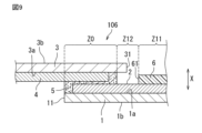
- Fig. 9 is a partial cross-sectional view of a stretchable device 106 according to the seventh embodiment.
- the stretchable device 106 according to the seventh embodiment is different from the stretchable device 100 according to the first embodiment in that a connecting member is provided.
- the stretchable device 106 of the seventh embodiment further includes a connection member 5.
- the connection member 5 is shown in FIG. 9 with hatching.
- the connection member 5 electrically connects the first wiring 2 and the second wiring 4.
- the region where the first wiring 2 and the second wiring 4 overlap and the region where the connection member 5 exists constitute a wiring region Z0 where the first wiring 2 and the second wiring 4 are electrically connected.
- connection member 5 is located between the first wiring 2 and the second wiring 4.
- a part of the connection member 5 is located outside the end of the first wiring 2 so as to cover the end of the first wiring 2 in the extension direction.
- a part of the connection member 5 is located outside the end of the second wiring 4 so as to cover the end of the second wiring 4 in the extension direction.
- Examples of the connection member 5 include ACF (Anisotropic Conductive Film), conductive paste, solder, etc.
- the connection member 5 preferably contains resin and conductive particles. The conductive particles contained in the connection member 5 come into contact with the first wiring 2 and the second wiring 4, thereby electrically connecting the first wiring 2 and the second wiring 4.
- connection member 5 connects the first wiring 2 and the second wiring 4.
- the connection member 5 also contacts the first main surface 1a of the first substrate 1 and the first main surface 3a of the second substrate 3, connecting the first substrate 1 and the second substrate 3.
- the connection of the stretchable device 106 will be described.
- the first substrate 1 and the second substrate 3 may be pressure-bonded, such as by applying pressure.
- the connection member 5 is deformed and the overall thickness changes. In other words, the stretchable device 106 can be made low-profile.
- the connection member 5 containing conductive particles is provided between the first wiring 2 and the second wiring 4, if the distance between the first wiring 2 and the second wiring 4 in the first direction X is greater than the maximum diameter of the conductive particles, electrical continuity cannot be achieved. In such a case, by performing pressure bonding as described above, the distance between the first wiring 2 and the second wiring 4 in the first direction X is reduced. Therefore, the electrical connection between the first wiring 2 and the second wiring 4 can be more reliably achieved.
- first wiring 2 and the second wiring 4 are electrically connected before crimping, crimping does not have to be performed. Also, if the connection member 5 has adhesive properties, crimping does not have to be performed. Also, there are no particular limitations on the crimping method.
- Fig. 10 is a partial cross-sectional view of a stretchable device 107 according to the eighth embodiment.
- the stretchable device 107 according to the eighth embodiment is different from the stretchable device 106 according to the seventh embodiment in the length of the second base material.
- the second substrate 3 extends in the first direction X to a position where it overlaps the first protective layer 6. Specifically, the second substrate end 31 of the second substrate 3 overlaps the first protective layer 6 when viewed from a direction perpendicular to the first direction X. In other words, the second substrate 3 overlaps the first non-overlapping region Z12. This allows the second substrate 3 to protect the exposed portion of the first wiring 2 located in the first non-overlapping region Z12.
- a first base material having elasticity A first wiring provided on a first main surface of the first base material; a second base material that faces the first base material in a first direction that is a thickness direction of the first base material and is connected to the first base material; a first wiring layer provided on a first main surface of the second base material and facing the first wiring in the first direction; A second wiring electrically connected to the first wiring; a first protective layer provided on the first main surface of the first base material so as to cover a portion of the first wiring; A stretchable device, wherein a first overlap region where the first base material and the first protective layer overlap when viewed from the first direction is separated from a wiring region where the first wiring and the second wiring are electrically connected.
- a second protective layer is provided on the first main surface of the second base material
- the stretchable device according to ⁇ 1> wherein a second overlapping region where the second base material and the second protective layer overlap when viewed from the first direction is separated from the wiring region.
- the stretchable device according to ⁇ 1> or ⁇ 2> further comprising a third protective layer provided on the second main surface of the first substrate.
- ⁇ 5> The stretchable device according to any one of ⁇ 1> to ⁇ 4>, further comprising a first insulating layer covering at least a portion of the exposed surface of the first wiring.
- ⁇ 6> The stretchable device according to any one of ⁇ 1> to ⁇ 5>, further comprising a second insulating layer covering at least a portion of the exposed surface of the second wiring.
- ⁇ 7> The stretchable device according to any one of ⁇ 1> to ⁇ 6>, further comprising a third insulating layer between the first wiring and the first base material.
- ⁇ 8> The stretchable device according to any one of ⁇ 1> to ⁇ 7>, further comprising a fourth insulating layer between the second wiring and the second base material.
- ⁇ 9> The stretchable device according to any one of ⁇ 1> to ⁇ 8>, further comprising a first covering layer covering the first main surface side of the first base material.
- ⁇ 10> The stretchable device according to ⁇ 9>, wherein the first covering layer overlaps the first protective layer when viewed from the first direction.
- ⁇ 11> The stretchable device according to any one of ⁇ 1> to ⁇ 10>, further comprising a second covering layer covering the first main surface side of the second base material.
- ⁇ 12> The stretchable device according to ⁇ 11>, wherein the second covering layer continuously covers the first main surface side of the second substrate and the second main surface side of the first substrate.
- Stretchable device 1 First substrate 1a First main surface 1b Second main surface 11 End of first substrate 2 First wiring 3 Second substrate 3a First main surface 3b Second main surface 31 End of second substrate 4 Second wiring 5 Connection member 6 First protective layer 61 End of first protective layer 7 Second protective layer 71 End of second protective layer 8 Third protective layer 9 Fourth protective layer 21 First insulating layer 22 Second insulating layer 23 Third insulating layer 24 Fourth insulating layer 41 First covering layer 42 Second covering layer X First direction Z0 Wiring region Z11 First overlapping region Z12 First non-overlapping region Z21 Second overlapping region Z22 Second non-overlapping region
Landscapes
- Engineering & Computer Science (AREA)
- Microelectronics & Electronic Packaging (AREA)
- Manufacturing & Machinery (AREA)
- Structure Of Printed Boards (AREA)
Abstract
伸縮性デバイスは、伸縮性を有する第1基材と、第1基材の第1主面上に設けられた第1配線と、第1基材の厚み方向である第1方向において第1基材と対向し、第1基材と接続される第2基材と、第2基材の第1主面上に設けられ、第1方向において第1配線と対向し、第1配線に電気的に接続された第2配線と、第1配線の一部を覆うように第1基材の第1主面上に設けられた第1保護層とを備える。第1方向から見て、第1基材と第1保護層とが重なる第1重複領域は、第1配線と第2配線とが電気的に接続される配線領域から離隔している。
Description
本開示は、伸縮性デバイスに関する。
従来、伸縮性デバイスとしては、特開2008-108890号公報(特許文献1)に記載されたものがある。この伸縮性デバイスは、第1基材と、第1基材上に設けられた第1配線と、第1基材の厚み方向において第1基材と対向する第2基材と、第2基材上に設けられ厚み方向において第1配線と対向する第2配線と、第1配線と第2配線を電気的に接続する接続部材とを有する。厚み方向からみて、第1配線と第2配線とが重なる領域と、接続部材が存在する領域とは、第1配線と前記第2配線とが電気的に接続される配線領域を構成する。厚み方向からみて、配線領域は、第1基材と第2基材とが重なる基材重複領域と一致している。
ところで、前記従来の伸縮性デバイスでは、配線が外側に露出している場合、水滴や異物が隣り合う配線間をまたいで付着した場合に、隣り合う配線間の短絡が発生して伸縮性デバイスが破損するおそれがある。また、金属配線が空気や湿気に触れることで、配線の酸化や腐食が発生するおそれがある。そこで、配線の表面を保護層で覆うことが考えられる。具体的に述べると、保護層は、第1配線において第2基材から露出している全ての部分に設けられる。つまり、厚み方向から見て、第1配線と前記第2配線とが電気的に接続される配線領域と、第1基材と保護層とが重なる保護層重複領域とが、隣接している。
しかしながら、伸縮性デバイスを伸縮する際、厚み方向から見て、配線領域と保護層重複領域との間において、第1配線の破断などの伸縮性デバイスの損傷が発生するおそれがあり、また、第1配線の抵抗値の上昇などの伸縮性デバイスの性能が低下するおそれがあることがわかった。
そこで、本開示の目的は、伸縮性デバイスの伸縮の際、伸縮性デバイスの損傷を低減でき、また、伸縮性デバイスの性能の低下を抑制できる伸縮性デバイスを提供することにある。
前記課題を解決するため、本開示の一態様である伸縮性デバイスは、
伸縮性を有する第1基材と、
前記第1基材の第1主面上に設けられた第1配線と、
前記第1基材の厚み方向である第1方向において前記第1基材と対向し、前記第1基材と接続される第2基材と、
前記第2基材の第1主面上に設けられ、前記第1方向において前記第1配線と対向し、前記第1配線に電気的に接続された第2配線と、
前記第1配線の一部を覆うように前記第1基材の前記第1主面上に設けられた第1保護層と
を備え、
前記第1方向から見て、前記第1基材と前記第1保護層とが重なる第1重複領域は、前記第1配線と前記第2配線とが電気的に接続される配線領域から離隔している。
伸縮性を有する第1基材と、
前記第1基材の第1主面上に設けられた第1配線と、
前記第1基材の厚み方向である第1方向において前記第1基材と対向し、前記第1基材と接続される第2基材と、
前記第2基材の第1主面上に設けられ、前記第1方向において前記第1配線と対向し、前記第1配線に電気的に接続された第2配線と、
前記第1配線の一部を覆うように前記第1基材の前記第1主面上に設けられた第1保護層と
を備え、
前記第1方向から見て、前記第1基材と前記第1保護層とが重なる第1重複領域は、前記第1配線と前記第2配線とが電気的に接続される配線領域から離隔している。
本開示の一態様である伸縮性デバイスによれば、伸縮性デバイスの伸縮の際、伸縮性デバイスの損傷を低減でき、また、伸縮性デバイスの性能の低下を抑制できる。
以下、本開示の実施形態について、図面を用いて詳細に説明する。各々の実施形態では、その実施形態以前に説明した点と異なる点について主に説明する。特に、同様の構成による同様の作用効果については実施形態ごとには逐次言及しない。以下の実施形態における構成要素のうち、独立請求項に記載されていない構成要素については、任意の構成要素として説明される。また、図面に示される構成要素の大きさおよび大きさの比は、必ずしも厳密ではない。また、各図において、実質的に同一の構成に対しては同一の符号を付しており、重複する説明は省略又は簡略化する場合がある。
[第1実施形態]
図1と図2と図3を参照しながら、第1実施形態に係る伸縮性デバイス100の構造について説明する。図1は、伸縮性デバイスの100の一部上面図である。図2は、伸縮性デバイス100の平面分解図である。図3は、伸縮性デバイス100の図1におけるIII-III断面図である。なお、本明細書中の断面図は、第1基材の厚み方向である第1方向から見て、第1基材1と第2基材3が重なる領域を含み、第1方向に平行な断面図である。第1方向を両矢印Xで示している。第1基材1の厚み方向と、第2基材3の厚み方向と、第1方向Xとは一致している。
図1と図2と図3を参照しながら、第1実施形態に係る伸縮性デバイス100の構造について説明する。図1は、伸縮性デバイスの100の一部上面図である。図2は、伸縮性デバイス100の平面分解図である。図3は、伸縮性デバイス100の図1におけるIII-III断面図である。なお、本明細書中の断面図は、第1基材の厚み方向である第1方向から見て、第1基材1と第2基材3が重なる領域を含み、第1方向に平行な断面図である。第1方向を両矢印Xで示している。第1基材1の厚み方向と、第2基材3の厚み方向と、第1方向Xとは一致している。
伸縮性デバイス100は、第1基材1と第2基材3と第1配線2と第2配線4と第1保護層6とを備える。第1基材1と第2基材3は、接続されている。第1基材1の第1主面1a上に設けられた第1配線2と、第2基材3の第1主面3a上に設けられた第2配線4とは、電気的に接続されている。第1保護層6は、第1配線2の一部を覆うように第1基材1の第1主面1a上に設けられている。
なお、伸縮性デバイス100の形状は特に限定されない。本明細書中では2つの基材が接続されている構造を実施例として説明するが、3つ以上の基材が接続されていてもよい。また、第1配線2は図1のような配置に限定されず、延伸方向も限定されない。具体的には、第1基材1の長手方向と第1配線2の延伸方向が一致していなくてもよいし、1方向に延伸していなくてもよい。また、第1配線2の本数は特に限定されず、1本であってもよいし複数であってもよい。第1配線2が複数である場合、第2配線4と電気的に接続されていない配線を含んでいてもよい。第2配線4の配置および本数についても同様である。
また、本明細書中における「上」とは、伸縮性デバイス100の使用時における上下と一致していなくてもよい。より具体的には、「第1基材1の主面上」とは、重力方向に規定される鉛直上方のような絶対的な一方向ではなく、第1基材1の主面を基準に、当該主面を境界とする外側と内側とのうち、外側に向かう方向を指す。「第2基材3の主面上」についても同様である。また、ある要素に対して「上方(above)」には、当該要素とは離れた上方、すなわち当該要素上の他の物体を介した上側の位置や間隔を空けた上側の位置だけではなく、当該要素と接する直上の位置(on)も含む。
以下、これらの構成要素およびその配置について説明する。図1と図2と図3に示すように、第1基材1と第2基材3とは、第1方向Xにおいて対向し、かつ、第1方向Xから見て、一部が重なる。同様に、第1配線2と第2配線4とは、第1方向Xにおいて対向する。
第1基材1は伸縮性を有する。第1基材1が伸縮性を有することで、第1配線2の伸縮を抑制せず、伸縮性デバイス100の使用時の伸縮における破断の危険性を低減することができる。
伸縮性を有する基材の例として、伸縮性を有する樹脂材料から構成されるシート状あるいはフィルム状の基材が挙げられる。樹脂材料としては、例えば、アクリル系樹脂、スチレン系樹脂、及び、ウレタン系樹脂からなる群より選択される少なくとも一種の樹脂を含むことが好ましい。ウレタン系樹脂としては、例えば、熱可塑性ポリウレタンが挙げられる。第1基材1の厚さは特に限定されないが、生体に貼り付けた際に生体表面の伸縮を阻害しない観点からは、1mm以下であることが好ましく、100μm以下であることがより好ましく、50μm以下であることがさらに好ましい。また、第1基材1の厚さは、1μm以上であることがより好ましい。
第1基材1は、互いに反対側に位置する第1主面1aおよび第2主面1bを有する。第1基材1は、第1主面1aおよび第2主面1bを接続する第1基材端部11を有する。第1基材端部11は、第1基材1のうち、第2基材3により近い端部である、言い換えれば、第1方向Xから見て、第2配線4と重なる端部である。具体的には、図1における上下方向の両端部のうち、第2基材3により近い端部であって、図3における左右方向の両端部のうち、第2基材3により近い端部である。なお、図1と図2と図3において、第1基材端部11と異なる端部は図示していない。
第1配線2は、第1基材1の第1主面1a上に設けられている。第1配線2は、好ましくは伸縮性を有する。第1配線2の材料として、例えば、導電性粒子としてのAg、Cu、および/またはNiなどの金属粉と、シリコーン樹脂などのエラストマー系樹脂とからなる混合物が挙げられる。導電性粒子の平均粒径は特に限定されるものではないが、0.01μm以上、10μm以下であることが好ましい。また、導電性粒子の形状は球形であることが好ましく、球形に限らず、伸縮性を良くするための扁平形や突起を有する構造でも良い。また、エラストマー系樹脂は、エポキシ系樹脂、ウレタン系樹脂、アクリル系樹脂、及び、シリコーン系樹脂からなる群より選択される少なくとも一種の樹脂(エラストマー系樹脂)を含み、伸縮性を確保する上で好ましい。
第1配線2の厚みは、好ましくは100μm以下であり、より好ましくは50μm以下である。また、伸縮性配線の厚みは、より好ましくは1μm以上である。また、第1配線の厚みや幅、長さは特に限定されない。なお、第1配線2は、伸縮性を有していなくてもよい。
第1配線2を第1基材1上に形成する方法を説明する。第1配線2の材料が、例えばAg及び樹脂の混合物を含有する導電性ペーストである場合、導電性ペーストを第1基材1に塗布する。塗布の方法は、スクリーン印刷、グラビア印刷またはインクジェット印刷であってもよい。その後、導電性ペーストを所定の抵抗値が得られるように熱硬化させることによって、第1配線2を第1基材1上に形成する。
第2基材3は、好ましくは伸縮性を有する。第2基材3は、好ましくは第1配線2よりも大きいヤング率を有する。具体的には、FPC(Flexible Printed Circuit)やFFC(Flexible Flat Cable)、PCB(Printed Circuit Board)等の基板が挙げられる。第1配線2よりもヤング率を大きくすることで、圧着時に接合部に圧力をよりかかりやすくし、低圧力で接合を可能にする。すなわち、低圧力化することで、接合時の基材へのダメージを低減することができる。また、第2基材3は、第1基材1よりも大きいヤング率を有することが好ましい。接続時の衝撃に強くなるため、接続信頼性をより向上させることができる。
第2基材3は、互いに反対側に位置する第1主面3aおよび第2主面3bを有する。第2基材3は、第1主面3aおよび第2主面3bを接続する第2基材端部31を有する。第2基材端部31は、第2基材3の、第1基材1により近い端部である、言い換えれば、第1方向Xから見て、第1配線2と重なる端部である。具体的には、図1における上下方向の両端部のうち、第1基材1により近い端部であって、図3における左右方向の両端部のうち、第1基材1により近い端部である。なお、図1と図2と図3において、第2基材端部31と異なる端部は図示していない。
第2基材3は、第1基材1と接続される。つまり、第1基材1の第1主面1aと第2基材3の第1主面3aとは、溶着などにより直接に接続されている。具体的に述べると、第1基材1の第1主面1aと第2基材3の第1主面3aとは、熱圧着されている。なお、第1基材1と第2基材3は、例えば、熱可塑性接着剤などの接着部材を介して、接続されていてもよい。
なお、第2基材3は伸縮性を有していなくてもよい。第2基材3の材料としては、例えば、PETやポリイミド等のシート状あるいはフィルム状の基材や、FPCやFFC、PCBなどの基板が挙げられる。また、第2基材3の材料は、第1基材1の材料と同じであってもよい。
第2配線4は、第2基材3の第1主面3a上に設けられている。第2配線4は、好ましくは伸縮性を有する。第2配線4は、好ましくは第1配線2よりも大きいヤング率を有する配線である。例えば、銅箔などの金属配線が挙げられる。第2配線4の厚みは、好ましくは1μm以上100μm以下であり、より好ましくは50μm以下である。第1配線2と第2配線4は、直接に接触して電気的に接続される。なお、第2配線4は、伸縮性を有していなくてもよい。また、第2配線4の材料は、第1配線2の材料と同じであってもよい。
第2配線4は、第1配線2に電気的に接続される。具体的に述べると、第1配線2と第2配線4とは、接触して電気的に接続される。第1方向Xから見て、第1配線2と第2配線4とが重なる領域は、第1配線2と第2配線4とが電気的に接続される配線領域Z0を構成する。
なお、第1配線2と第2配線4は、導電性を有する接続部材を介して、電気的に接続されていてもよい。このとき、第1方向Xから見て、第1配線2と第2配線4とが重なる領域と、接続部材が存在する領域とは、第1配線2と第2配線4とが電気的に接続される配線領域Z0を構成する。
なお、第1配線2と第2配線4は、導電性を有する接続部材を介して、電気的に接続されていてもよい。このとき、第1方向Xから見て、第1配線2と第2配線4とが重なる領域と、接続部材が存在する領域とは、第1配線2と第2配線4とが電気的に接続される配線領域Z0を構成する。
第1保護層6は、第1配線2の一部を覆うように第1基材1の第1主面1a上に設けられている。このように、第1保護層6は、第1配線2の一部を覆うため、水滴や異物が隣り合う第1配線2の間をまたいで付着しても、隣り合う第1配線2の間の短絡を抑制でき、また、第1配線2が空気や湿気に触れることを低減して、第1配線2の酸化や腐食の発生を抑制できる。なお、第1保護層6は、全ての第1配線2を一体に覆うように設けられていてもよく、または、第1保護層6は、それぞれの第1配線2を個別に覆うように分割して設けられていてもよい。
具体的に述べると、第1保護層6は、第1配線2の一部を覆い第1基材1の第1主面1aに接触し、第1方向Xから見て第1基材1と重なっている。好ましくは、第1保護層6は、第1基材1における第1配線2から露出する領域の一部に接触する。なお、第1保護層6は、第1配線2を覆い第1基材1に接触しなくてもよい。
第1保護層6の例として具体的には樹脂材料、又は、樹脂材料および無機材料からなる混合物であることが好ましく、樹脂材料として例えば、ウレタン系、スチレン系、オレフィン系、シリコーン系、フッ素系、ニトリルゴム、ラテックスゴム、塩化ビニル、エステル系、アミド系等のエラストマー系樹脂、エポキシ、フェノール、アクリル、ポリエステル、イミド系、ロジン、セルロース、ポリエチレンテレフタレート系、ポリエチレンナフタレート系、ポリカーボネート系樹脂が挙げられる。また、第1保護層6は絶縁性を有することが好ましい。第1保護層6が絶縁性を有することで、第1配線6のイオンマイグレーションをより確実に抑制することができる。第1保護層6は、例えば、絶縁材料の塗布やラミネート材の貼り付けにより設けられる。
第1保護層6の厚みは1μm以上100μm以下であることが好ましく、50μm以下であることがより好ましい。第1保護層6の厚みを1μm以上とすることで、第1保護層6の耐久性を確保することができる。また、第1保護層6の厚みを100μm以下にすることで、全体を低背化させることができる。なお、第1保護層6の厚みが一定でない場合、第1保護層6の第1方向Xにおける最大の寸法を厚みとする。
また、第1保護層6は第1保護層端部61を有する。第1保護層端部61は、第1保護層6のうち、第1基材端部11により近い端部である、具体的には、図1における上下方向の両端部のうち、第1基材端部11により近い端部であって、図3における左右方向の両端部のうち、第1基材端部11により近い端部である。なお、図1と図2と図3において、第1保護層端部61と異なる端部は図示していない。
第1方向Xから見て、第1基材1と第1保護層6とが重なる第1重複領域Z11は、第1配線2と第2配線4とが電気的に接続される配線領域Z0から離隔している。具体的に述べると、第1方向Xから見て、第1保護層端部61と第2配線4の端部とは、離隔している。第1方向Xから見て、配線領域Z0と第1重複領域Z11とは、第1配線2の延伸方向において離隔している。この実施形態では、第1配線2の延伸方向と第2配線4の延伸方向とは、一致している。
上記構成によれば、第1方向Xから見て、第1重複領域Z11は、配線領域Z0から離隔しているので、第1方向Xから見て、第1重複領域Z11と配線領域Z0との間に、第1基材1のうちの第1保護層6と重ならない第1非重複領域Z12が存在する。つまり、第1方向Xから見て、第1保護層端部61と第2配線4の端部の間に、第1非重複領域Z12が存在する。
これにより、伸縮性デバイス100を伸縮する際、伸縮性デバイス100にかかる応力を第1非重複領域Z12において緩和することができる。したがって、第1配線2の破断などの伸縮性デバイス100の損傷を低減でき、また、第1配線2の抵抗値の上昇などの伸縮性デバイス100の性能の低下を抑制できる。
要するに、配線領域Z0では、第1配線2と第2配線4と第1基材1と第2基材3とが重なっているため、第1基材1の伸縮性能が低下し、伸縮性デバイス100において剛性の大きな部分となる。また、第1重複領域Z11では、第1基材1と第1配線2と第1保護層6とが重なっているため、第1基材1の伸縮性能が低下し、伸縮性デバイス100において剛性の大きな部分となる。一方、第1非重複領域Z12では、第1基材1は第1保護層6に覆われていないため、第1基材1の伸縮性能を確保でき、伸縮性デバイス100において伸縮性を有する部分となる。このため、伸縮性デバイス100を伸縮する際、剛性の大きな部分にかかる応力を第1非重複領域Z12で吸収できる。
つまり、本願発明者は、伸縮性デバイス100を伸縮する際、剛性の大きな部分に局所的に応力が集中することに着目した。さらに、本願発明者は、配線領域Z0における積層数(第1配線2と第2配線4と第1基材1と第2基材3の4層)と第1重複領域Z11における積層数(第1基材1と第1配線2と第1保護層6の3層)が異なることから、配線領域Z0の剛性と第1重複領域Z11の剛性が異なることに着目した。そして、本願発明者は、従来のように第1方向Xから見て配線領域Z0と第1重複領域Z11が隣接している場合、配線領域Z0と第1重複領域Z11の間において応力が集中することを見出した。このような見地から、本願発明者は、この応力が集中する部分(つまり、配線領域Z0と第1重複領域Z11の間)を、伸縮性を有する部分(つまり、第1非重複領域Z12)とすることで、応力を緩和することができる伸縮性デバイス100を実現することに至った。
好ましくは、第1方向Xから見て、第1重複領域Z11と配線領域Z0の間の最短距離は、1μm以上30mm以下、より好ましくは、1μm以上10mm以下である。つまり、第1方向Xから見て、第1配線2の延伸方向における第1保護層端部61と第2基材端部31の間の最短距離は、1μm以上30mm以下である。したがって、最短距離が1μm以上であるので、第1非重複領域Z12において第1基材1の伸縮性能を向上できて、第1非重複領域Z12において応力緩和を向上できる。また、最短距離が30mm以下であるので、第1非重複領域Z12において第1基材1の伸縮性能を十分に確保でき、かつ、第1配線2の露出を低減して隣り合う第1配線2間の短絡を低減できる。
次に、伸縮性デバイス100における接続について説明する。第1基材1と第2基材3とを接続する場合、第1基材1と第2基材3とを、加熱と加圧を行って熱圧着する。これにより、第1基材1と第2基材3が接続される。なお、第1基材1と第2基材3の圧着方法は特に限定されない。また、第1配線2と第2配線4は接触して電気的に接続される。
[第2実施形態]
次に、図4を参照して、第2実施形態について説明する。図4は第2実施形態に係る伸縮性デバイス101の一部断面図である。第2実施形態に係る伸縮性デバイス101は、第1実施形態に係る伸縮性デバイス100と比較して、第2保護層を設けている点が相違する。
次に、図4を参照して、第2実施形態について説明する。図4は第2実施形態に係る伸縮性デバイス101の一部断面図である。第2実施形態に係る伸縮性デバイス101は、第1実施形態に係る伸縮性デバイス100と比較して、第2保護層を設けている点が相違する。
図4に示すように、第2実施形態の伸縮性デバイス101では、さらに、第2保護層7を備える。第2保護層7の材料および厚みは、第1保護層6の材料および厚みと同じであるが、厚みが異なっていてもよく、同様に材料が異なっていてもよい。
第2保護層7は、第2配線4の一部を覆うように第2基材3の第1主面3a上に設けられている。このように、第2保護層7は、第2配線4の一部を覆うため、水滴や異物が隣り合う第2配線4の間をまたいで付着しても、隣り合う第2配線4の間の短絡を抑制でき、また、第2配線4が空気や湿気に触れることを低減して、第2配線4の酸化や腐食の発生を抑制できる。
具体的に述べると、第2保護層7は、第2配線4の一部を覆い第2基材3の第1主面3aに接触し、第1方向Xから見て第2基材3と重なっている。好ましくは、第2保護層7は、第2基材3における第2配線4から露出する領域の一部に接触する。なお、第2保護層7は、第2配線4を覆い第2基材3に接触しなくてもよい。
第2保護層7は第2保護層端部71を有する。第2保護層端部71は、第2保護層7のうち、第2基材端部31により近い端部である、具体的には、図4における左右方向の両端部のうち、第2基材端部31により近い端部である。なお、図4において、第2保護層端部71と異なる端部は図示していない。
第1方向Xから見て、第2基材3と第2保護層7とが重なる第2重複領域Z21は、配線領域Z0から離隔している。具体的に述べると、第1方向Xから見て、第2保護層端部71と第1基材端部11とは、離隔している。第1方向Xから見て、配線領域Z0と第2重複領域Z21とは、第2配線4の延伸方向において離隔している。この実施形態では、第1配線2の延伸方向と第2配線4の延伸方向とは、一致している。
上記構成によれば、第1方向Xから見て、第2重複領域Z21は、配線領域Z0から離隔しているので、第1方向Xから見て、第2重複領域Z21と配線領域Z0との間に、第2基材3のうちの第2保護層7と重ならない第2非重複領域Z22が存在する。つまり、第1方向Xから見て、第2保護層端部71と第1基材端部11の間に、第2非重複領域Z22が存在する。
これにより、伸縮性デバイス101を伸縮する際、伸縮性デバイス101にかかる応力を第2非重複領域Z22において緩和することができる。特に、第2基材3が伸縮性を有する場合、第2配線4の破断などの伸縮性デバイス101の損傷を低減でき、また、第2配線4の抵抗値の上昇などの伸縮性デバイス101の性能の低下を抑制できる。
[第3実施形態]
次に、図5を参照して、第3実施形態について説明する。図5は第3実施形態に係る伸縮性デバイス102の一部断面図である。第3実施形態に係る伸縮性デバイス102は、第2実施形態に係る伸縮性デバイス101と比較して、第3保護層および第4保護層を設けている点が相違する。
次に、図5を参照して、第3実施形態について説明する。図5は第3実施形態に係る伸縮性デバイス102の一部断面図である。第3実施形態に係る伸縮性デバイス102は、第2実施形態に係る伸縮性デバイス101と比較して、第3保護層および第4保護層を設けている点が相違する。
図5に示すように、第3実施形態の伸縮性デバイス102では、さらに、第3保護層8および第4保護層9を備える。第3保護層8および第4保護層9の材料および厚みは、第1保護層6の材料および厚みと同じであるが、厚みが異なっていてもよく、同様に材料が異なっていてもよい。
第3保護層8は、第1基材1の第2主面1b上に設けられている。第3保護層8は、第1基材1の第2主面1bの全面を覆うことが好ましいが、第1基材1の第2主面1bの少なくとも一部を覆っていればよい。上記構成によれば、第3保護層8により第1基材1の防水性能が向上する。また、第3保護層8に生体適合性を有する材料を用いることで、生体適合性が向上する。
第4保護層9は、第2基材3の第2主面3b上に設けられている。第4保護層9は、第2基材3の第2主面3bの全面を覆うことが好ましいが、第2基材3の第2主面3bの一部を覆っていてもよい。上記構成によれば、第4保護層9により第2基材3の防水性能が向上する。また、第4保護層9に生体適合性を有する材料を用いることで、生体適合性が向上する。
なお、第3保護層8および第4保護層9のうちの何れか一方のみを設けてもよい。また、第1実施形態に係る伸縮性デバイス100に対して、第3保護層8および第4保護層9のうちの少なくとも一方を設けてもよい。
[第4実施形態]
次に、図6を参照して、第4実施形態について説明する。図6は第4実施形態に係る伸縮性デバイス103の一部断面図である。第4実施形態に係る伸縮性デバイス103は、第1実施形態に係る伸縮性デバイス100と比較して、第1絶縁層および第2絶縁層を設けている点が相違する。
次に、図6を参照して、第4実施形態について説明する。図6は第4実施形態に係る伸縮性デバイス103の一部断面図である。第4実施形態に係る伸縮性デバイス103は、第1実施形態に係る伸縮性デバイス100と比較して、第1絶縁層および第2絶縁層を設けている点が相違する。
図6に示すように、第4実施形態の伸縮性デバイス103では、さらに、第1絶縁層21および第2絶縁層22を備える。第1絶縁層21および第2絶縁層22の材料は、第1保護層6の材料と異なる。
第1絶縁層21および第2絶縁層22としては、第1基材1よりも吸水率の少ないものが好ましい。第1絶縁層21および第2絶縁層22の材料としては、例えば、シリコーン系樹脂、アクリル系樹脂、オレフィン系樹脂、変性ウレタン系樹脂、塩化ビニル系樹脂、ポリエステル系、ポリアミド系、ポリオレフィン系、ポリエチレン系、ポリプロピレン系の樹脂材料が挙げられる。第1絶縁層21および第2絶縁層22は、例えば印刷によって形成される。
第1絶縁層21は、第1配線2の露出面の少なくとも一部を覆う。第1配線2の露出面は、第1配線2の外面のうちの外部に露出している面である。具体的に述べると、第1配線2の露出面は、第1配線2のうちの第1基材1と第1保護層6と第2配線4に覆われていない面である。第1絶縁層21は、第1配線2の露出面の全面を覆うことが好ましいが、第1配線2の露出面の一部を覆っていてもよい。また、第1絶縁層21は、好ましくは、第1配線2と第1保護層6との間にも存在する。また、第1絶縁層21は、第1方向Xにおいて、第2配線4と重なっていないが、第1絶縁層21の一部が、第1方向Xにおいて、第2配線4と重なっていてもよい。上記構成によれば、第1絶縁層21により、水滴や異物による隣り合う第1配線2間の短絡を防ぎ、信頼性が向上する。
ここで、第1絶縁層21を形成する方法を説明すると、第1絶縁層21の材料となる絶縁ペーストを、第1配線2上にスクリーン印刷法等を用いて印刷する。このとき、第1配線2の延伸方向に直交する断面において、絶縁ペーストを、第1配線2の幅よりも1μm以上10mm以下に大きく印刷するのがよく、より好ましくは、20μm以上1000μm以下に大きく印刷するのがよい。
第2絶縁層22は、第2配線4の露出面の少なくとも一部を覆う。第2配線4の露出面は、第2配線4の外面のうちの外部に露出している面である。具体的に述べると、第2配線4の露出面は、第2配線4のうちの第2基材3と第1配線2に覆われていない面である。第2絶縁層22は、第2配線4の露出面の全面を覆うことが好ましいが、第2配線4の露出面の一部を覆っていてもよい。また、第2絶縁層22は、第1方向Xにおいて、第1配線2と重なっていないが、第2絶縁層22の一部が、第1方向Xにおいて、第1配線2と重なっていてもよい。上記構成によれば、第2絶縁層22により、水滴や異物による隣り合う第2配線4間の短絡を防ぎ、信頼性が向上する。
なお、第1絶縁層21および第2絶縁層22のうちの何れか一方のみを設けてもよい。また、第2、第3実施形態に係る伸縮性デバイス101,102に対して、第1絶縁層21および第2絶縁層22のうちの少なくとも一方を設けてもよい。
[第5実施形態]
次に、図7を参照して、第5実施形態について説明する。図7は第5実施形態に係る伸縮性デバイス104の一部断面図である。第5実施形態に係る伸縮性デバイス104は、第4実施形態に係る伸縮性デバイス103と比較して、第3絶縁層および第4絶縁層を設けている点が相違する。
次に、図7を参照して、第5実施形態について説明する。図7は第5実施形態に係る伸縮性デバイス104の一部断面図である。第5実施形態に係る伸縮性デバイス104は、第4実施形態に係る伸縮性デバイス103と比較して、第3絶縁層および第4絶縁層を設けている点が相違する。
図7に示すように、第5実施形態の伸縮性デバイス104では、さらに、第3絶縁層23および第4絶縁層24を備える。第3絶縁層23および第4絶縁層24の材料は、第1絶縁層21および第2絶縁層22の材料と同じであってよく、または各々異なる材料であってもよい。
第3絶縁層23は、第1方向Xにおいて、第1配線2と第1基材1の間に配置されている。言い換えれば、第3絶縁層23は、第1基材1の第1主面1a上に設けられ、第1配線2の下面(すなわち、第1基材1の第1主面1aと対向する第1配線2の面)と接触している。
第1基材1が透湿性を有する場合、第1基材1から第1配線2に水分が侵入し、イオンマイグレーションが発生するおそれがある。第3絶縁層23を備えることで、第1基材1から第1配線2への水分の侵入を抑制することができる。すなわち、第1配線2の短絡を抑制した伸縮性デバイス104が提供される。
第4絶縁層24は、第1方向Xにおいて、第2配線4と第2基材3の間に配置されている。言い換えれば、第4絶縁層24は、第2基材3の第1主面3a上に設けられ、第2配線4の下面(すなわち、第2基材3の第1主面3aと対向する第2配線4の面)と接触している。
第2基材3が透湿性を有する場合、第2基材3から第2配線4に水分が侵入し、イオンマイグレーションが発生するおそれがある。第4絶縁層24を備えることで、第2基材3から第2配線4への水分の侵入を抑制することができる。すなわち、第2配線4の短絡を抑制した伸縮性デバイス104が提供される。
なお、第3絶縁層23および第4絶縁層24のうちの何れか一方のみを設けてもよい。また、第1、第2、第3実施形態に係る伸縮性デバイス100,101,102に対して、第3絶縁層23および第4絶縁層24のうちの少なくとも一方を設けてもよい。
また、第3絶縁層23は、例えば第1配線2の下面のみを覆うように配置されていてもよいし、第1基材1の第1配線2が無い部分に配置されていてもよい。また、第3絶縁層23は、第1基材1全体を覆うように配置されていてもよい。また、第3絶縁層23は、第2配線2と接触していればよく、第1基材1と第3絶縁層23との間に異なる層が配置されていてもよい。第4絶縁層24についても、第3絶縁層23と同様であってもよい。
[第6実施形態]
次に、図8を参照して、第6実施形態について説明する。図8は第6実施形態に係る伸縮性デバイス105の一部断面図である。第6実施形態に係る伸縮性デバイス105は、第4実施形態に係る伸縮性デバイス103と比較して、第1被覆層および第2被覆層を設けている点が相違する。
次に、図8を参照して、第6実施形態について説明する。図8は第6実施形態に係る伸縮性デバイス105の一部断面図である。第6実施形態に係る伸縮性デバイス105は、第4実施形態に係る伸縮性デバイス103と比較して、第1被覆層および第2被覆層を設けている点が相違する。
図8に示すように、第6実施形態の伸縮性デバイス105では、さらに、第1被覆層41および第2被覆層42を備える。第1被覆層41および第2被覆層42の材料は、第1保護層6の材料と異なる。
第1被覆層41は、少なくとも第2基材3の第1基材側の端部を覆う。このような構造にすることで、第2基材3を外力から保護することができる。より好ましくは、第1被覆層41は、第1基材1の第1主面1a側を覆う。具体的に述べると、第1被覆層41は、第1基材1の第1主面1aの少なくとも一部と第1絶縁層21の少なくとも一部と第1保護層6の少なくとも一部と第2基材3の第2主面3bの少なくとも一部とを覆う。このような構成にすることで、第1配線2のうち、第1保護層6から露出している部分および第1保護層6を外力から保護することができる。
第1被覆層41の例として樹脂材料が挙げられる。例えば、第1被覆層41は、可撓性を有する樹脂であることが好ましい。具体的には、アイオノマー樹系脂、ポリエステル系樹脂、スチレン系樹脂、オレフィン系樹脂、エポキシ系樹脂、ウレタン系樹脂、アクリル系樹脂又はシリコーン系樹脂で形成されてよく、好ましくはシリコーン系樹脂で形成される。また、第1被覆層41は熱可塑性樹脂であってもよい。具体的には、熱可塑性ポリウレタン(TPU)、または、スチレン系樹脂として、スチレン-ブタジエン-スチレン共重合樹脂(SBS)が挙げられる。なお、第1被覆層41は複数の部材によって構成されていてもよい。第1被覆層41に樹脂を用いることで、接続部を外力からより好適に保護することができる。
第2被覆層42は、少なくとも第1基材1の第2基材側の端部を覆う。このような構造にすることで、第1基材1を外力から保護することができる。より好ましくは、第2被覆層42は、第2基材3の第1主面3a側を覆う。具体的に述べると、第2被覆層42は、第2基材3の第1主面3aの少なくとも一部と第2絶縁層22の少なくとも一部と第1基材1の第2主面1bの少なくとも一部とを覆う。上記のような構成にすることで、第2配線4のうち、第2絶縁層22から露出している部分および第2絶縁層22を外力から保護することができる。
第2被覆層42の例として樹脂材料が挙げられる。例えば、第1被覆層41は、可撓性を有する樹脂であることが好ましい。具体的には、アイオノマー樹系脂、ポリエステル系樹脂、スチレン系樹脂、オレフィン系樹脂、エポキシ系樹脂、ウレタン系樹脂、アクリル系樹脂又はシリコーン系樹脂で形成されてよく、好ましくはシリコーン系樹脂で形成される。また、第2被覆層42は熱可塑性樹脂であってもよい。具体的には、熱可塑性ポリウレタン(TPU)、または、スチレン系樹脂として、スチレン-ブタジエン-スチレン共重合樹脂(SBS)が挙げられる。なお、第2被覆層42は複数の部材によって構成されていてもよい。第2被覆層42に樹脂を用いることで、接続部を外力からより好適に保護することができる。また、第1被覆層41と第2被覆層42は同一の部材であってもよいし、異なる部材であってもよい。
第1保護層6、第1絶縁層21および第2絶縁層22などの樹脂を含む部材は、細胞毒性を有する場合がある。第1被覆層41を設けることで、細胞毒性を有する成分の漏出を抑制することができる。第2被覆層42についての効果も同様である。また、第1被覆層41および第2被覆層42を備えることで、より細胞毒性を有する成分の漏出を抑制することができる。
また、第1被覆層41は、第2基材3の第2主面3bと第1絶縁層21と第1保護層6とを連続して覆う。言い換えると、第1被覆層41は、配線領域Z0と第1非重複領域Z12と第1重複領域Z11とを連続して覆う。これにより、第1被覆層41は、配線領域Z0および第1重複領域Z11に対して凹部を構成する第1非重複領域Z12を覆うので、凹部を低減できる伸縮性デバイス105を提供できる。したがって、装着性を向上した伸縮性デバイス105を提供できる。
また、第1被覆層41は、第1方向Xから見て、第1保護層6に重なる。これにより、第1被覆層41は、第1保護層6上に配置されるので、第1基材1の第1主面1a側と第2基材3の第2主面3b側との段差が、第1保護層6の厚み分、軽減される。
また、第2被覆層42は、第2基材3の第1主面3a側および第1基材1の第2主面1b側を連続して覆う。これにより、第2基材3の第1主面3a側および第1基材1の第2主面1b側の損傷を防止できる。
なお、第1被覆層41および第2被覆層42のうちの何れか一方のみを設けてもよい。また、第1、第2、第3、第5実施形態に係る伸縮性デバイス100,101,102,104に対して、第1被覆層41および第2被覆層42のうちの少なくとも一方を設けてもよい。
[第7実施形態]
次に、図9を参照して、第7実施形態について説明する。図9は第7実施形態に係る伸縮性デバイス106の一部断面図である。第7実施形態に係る伸縮性デバイス106は、第1実施形態に係る伸縮性デバイス100と比較して、接続部材を設けている点が相違する。
次に、図9を参照して、第7実施形態について説明する。図9は第7実施形態に係る伸縮性デバイス106の一部断面図である。第7実施形態に係る伸縮性デバイス106は、第1実施形態に係る伸縮性デバイス100と比較して、接続部材を設けている点が相違する。
図9に示すように、第7実施形態の伸縮性デバイス106では、さらに、接続部材5を備える。図9では、便宜上、接続部材5をドットのハッチングで示している。接続部材5は、第1配線2と第2配線4とを電気的に接続する。このとき、第1方向Xから見て、第1配線2と第2配線4とが重なる領域と、接続部材5が存在する領域とは、第1配線2と第2配線4とが電気的に接続される配線領域Z0を構成する。
接続部材5の一部は、第1配線2と第2配線4の間に位置する。また、接続部材5の一部は、第1配線2の延在方向の端部を覆うように第1配線2の端部の外側に位置する。また、接続部材5の一部は、第2配線4の延在方向の端部を覆うように第2配線4の端部の外側に位置する。接続部材5の例としてはACF(Anisotropic Conductive Film)や導電性ペースト、はんだなどが挙げられる。接続部材5は、樹脂と導電性粒子を含むことが好ましい。接続部材5に含まれる導電性粒子が、第1配線2および第2配線4に接触することで、第1配線2と第2配線4とが電気的に接続される。
さらに、接続部材5は、第1配線2と第2配線4を接続する。また、接続部材5は、第1基材1の第1主面1aと第2基材3の第1主面3aに接触して、第1基材1と第2基材3を接続する。
次に、伸縮性デバイス106の接続について説明する。第1基材1と第2基材3とを接続する場合、第1基材1と第2基材3とを、加圧などの圧着を行ってもよい。そのような処理を行うことで、接続部材5が変形し、全体の厚みが変化する。すなわち、伸縮性デバイス106の、低背化を実現することができる。また、前述したように導電性粒子を含む接続部材5を第1配線2と第2配線4の間に設ける場合、第1方向Xにおける第1配線2と第2配線4との距離が導電性粒子の最大径より大きいと導通することができない。そのような場合、上記のような圧着を行うことで、第1方向Xにおける、第1配線2と第2配線4との距離が小さくなる。従って第1配線2と第2配線4との電気的な接続をより確実に行うことができる。
なお、圧着の前に第1配線2と第2配線4とが電気的に接続されていれば、圧着を行わなくてもよい。また、接続部材5が接着性を有していれば、圧着を行わなくてもよい。また、圧着方法は特に限定されない。
[第8実施形態]
次に、図10を参照して、第8実施形態について説明する。図10は第8実施形態に係る伸縮性デバイス107の一部断面図である。第8実施形態に係る伸縮性デバイス107は、第7実施形態に係る伸縮性デバイス106と比較して、第2基材の長さが相違する。
次に、図10を参照して、第8実施形態について説明する。図10は第8実施形態に係る伸縮性デバイス107の一部断面図である。第8実施形態に係る伸縮性デバイス107は、第7実施形態に係る伸縮性デバイス106と比較して、第2基材の長さが相違する。
図10に示すように、第8実施形態の伸縮性デバイス107では、第2基材3は、第1方向Xにおいて、第1保護層6に重なる位置まで延在している。具体的に述べると、第2基材3の第2基材端部31は、第1方向Xに直交する方向からみて、第1保護層6に重なる。つまり、第2基材3は、第1非重複領域Z12に重なる。これにより、第2基材3は、第1非重複領域Z12に位置する第1配線2の露出部分を保護することができる。
なお、本開示は上述の実施形態に限定されず、本開示の要旨を逸脱しない範囲で設計変更可能である。例えば、第1から第8実施形態のそれぞれの特徴点を様々に組み合わせてもよい。
本開示は以下の態様を含む。
<1>
伸縮性を有する第1基材と、
前記第1基材の第1主面上に設けられた第1配線と、
前記第1基材の厚み方向である第1方向において前記第1基材と対向し、前記第1基材と接続される第2基材と、
前記第2基材の第1主面上に設けられ、前記第1方向において前記第1配線と対向し、
前記第1配線に電気的に接続された第2配線と、
前記第1配線の一部を覆うように前記第1基材の前記第1主面上に設けられた第1保護層と
を備え、
前記第1方向から見て、前記第1基材と前記第1保護層とが重なる第1重複領域は、前記第1配線と前記第2配線とが電気的に接続される配線領域から離隔している、伸縮性デバイス。
<2>
さらに、前記第2基材の第1主面上に設けられた第2保護層を備え、
前記第1方向から見て、前記第2基材と前記第2保護層とが重なる第2重複領域は、前記配線領域から離隔している、<1>に記載の伸縮性デバイス。
<3>
さらに、前記第1基材の第2主面上に設けられた第3保護層を備える、<1>または<2>に記載の伸縮性デバイス。
<4>
さらに、前記第2基材の第2主面上に設けられた第4保護層を備える、<1>から<3>の何れか一つに記載の伸縮性デバイス。
<5>
さらに、前記第1配線の露出面の少なくとも一部を覆う第1絶縁層を備える、<1>から<4>の何れか一つに記載の伸縮性デバイス。
<6>
さらに、前記第2配線の露出面の少なくとも一部を覆う第2絶縁層を備える、<1>から<5>の何れか一つに記載の伸縮性デバイス。
<7>
さらに、前記第1配線と前記第1基材の間に第3絶縁層を備える、<1>から<6>の何れか一つに記載の伸縮性デバイス。
<8>
さらに、前記第2配線と前記第2基材の間に第4絶縁層を備える、<1>から<7>の何れか一つに記載の伸縮性デバイス。
<9>
さらに、前記第1基材の第1主面側を覆う第1被覆層を備える、<1>から<8>の何れか一つに記載の伸縮性デバイス。
<10>
前記第1被覆層は、前記第1方向から見て、前記第1保護層に重なる、<9>に記載の伸縮性デバイス。
<11>
さらに、前記第2基材の第1主面側を覆う第2被覆層を備える、<1>から<10>の何れか一つに記載の伸縮性デバイス。
<12>
前記第2被覆層は、前記第2基材の第1主面側および前記第1基材の第2主面側を連続して覆う、<11>に記載の伸縮性デバイス。
<1>
伸縮性を有する第1基材と、
前記第1基材の第1主面上に設けられた第1配線と、
前記第1基材の厚み方向である第1方向において前記第1基材と対向し、前記第1基材と接続される第2基材と、
前記第2基材の第1主面上に設けられ、前記第1方向において前記第1配線と対向し、
前記第1配線に電気的に接続された第2配線と、
前記第1配線の一部を覆うように前記第1基材の前記第1主面上に設けられた第1保護層と
を備え、
前記第1方向から見て、前記第1基材と前記第1保護層とが重なる第1重複領域は、前記第1配線と前記第2配線とが電気的に接続される配線領域から離隔している、伸縮性デバイス。
<2>
さらに、前記第2基材の第1主面上に設けられた第2保護層を備え、
前記第1方向から見て、前記第2基材と前記第2保護層とが重なる第2重複領域は、前記配線領域から離隔している、<1>に記載の伸縮性デバイス。
<3>
さらに、前記第1基材の第2主面上に設けられた第3保護層を備える、<1>または<2>に記載の伸縮性デバイス。
<4>
さらに、前記第2基材の第2主面上に設けられた第4保護層を備える、<1>から<3>の何れか一つに記載の伸縮性デバイス。
<5>
さらに、前記第1配線の露出面の少なくとも一部を覆う第1絶縁層を備える、<1>から<4>の何れか一つに記載の伸縮性デバイス。
<6>
さらに、前記第2配線の露出面の少なくとも一部を覆う第2絶縁層を備える、<1>から<5>の何れか一つに記載の伸縮性デバイス。
<7>
さらに、前記第1配線と前記第1基材の間に第3絶縁層を備える、<1>から<6>の何れか一つに記載の伸縮性デバイス。
<8>
さらに、前記第2配線と前記第2基材の間に第4絶縁層を備える、<1>から<7>の何れか一つに記載の伸縮性デバイス。
<9>
さらに、前記第1基材の第1主面側を覆う第1被覆層を備える、<1>から<8>の何れか一つに記載の伸縮性デバイス。
<10>
前記第1被覆層は、前記第1方向から見て、前記第1保護層に重なる、<9>に記載の伸縮性デバイス。
<11>
さらに、前記第2基材の第1主面側を覆う第2被覆層を備える、<1>から<10>の何れか一つに記載の伸縮性デバイス。
<12>
前記第2被覆層は、前記第2基材の第1主面側および前記第1基材の第2主面側を連続して覆う、<11>に記載の伸縮性デバイス。
100、101、102、103、104、105、106、107 伸縮性デバイス
1 第1基材
1a 第1主面
1b 第2主面
11 第1基材端部
2 第1配線
3 第2基材
3a 第1主面
3b 第2主面
31 第2基材端部
4 第2配線
5 接続部材
6 第1保護層
61 第1保護層端部
7 第2保護層
71 第2保護層端部
8 第3保護層
9 第4保護層
21 第1絶縁層
22 第2絶縁層
23 第3絶縁層
24 第4絶縁層
41 第1被覆層
42 第2被覆層
X 第1方向
Z0 配線領域
Z11 第1重複領域
Z12 第1非重複領域
Z21 第2重複領域
Z22 第2非重複領域
1 第1基材
1a 第1主面
1b 第2主面
11 第1基材端部
2 第1配線
3 第2基材
3a 第1主面
3b 第2主面
31 第2基材端部
4 第2配線
5 接続部材
6 第1保護層
61 第1保護層端部
7 第2保護層
71 第2保護層端部
8 第3保護層
9 第4保護層
21 第1絶縁層
22 第2絶縁層
23 第3絶縁層
24 第4絶縁層
41 第1被覆層
42 第2被覆層
X 第1方向
Z0 配線領域
Z11 第1重複領域
Z12 第1非重複領域
Z21 第2重複領域
Z22 第2非重複領域
Claims (12)
- 伸縮性を有する第1基材と、
前記第1基材の第1主面上に設けられた第1配線と、
前記第1基材の厚み方向である第1方向において前記第1基材と対向し、前記第1基材と接続される第2基材と、
前記第2基材の第1主面上に設けられ、前記第1方向において前記第1配線と対向し、前記第1配線に電気的に接続された第2配線と、
前記第1配線の一部を覆うように前記第1基材の前記第1主面上に設けられた第1保護層と
を備え、
前記第1方向から見て、前記第1基材と前記第1保護層とが重なる第1重複領域は、前記第1配線と前記第2配線とが電気的に接続される配線領域から離隔している、伸縮性デバイス。 - さらに、前記第2基材の第1主面上に設けられた第2保護層を備え、
前記第1方向から見て、前記第2基材と前記第2保護層とが重なる第2重複領域は、前記配線領域から離隔している、請求項1に記載の伸縮性デバイス。 - さらに、前記第1基材の第2主面上に設けられた第3保護層を備える、請求項1または2に記載の伸縮性デバイス。
- さらに、前記第2基材の第2主面上に設けられた第4保護層を備える、請求項1~3のいずれかに記載の伸縮性デバイス。
- さらに、前記第1配線の露出面の少なくとも一部を覆う第1絶縁層を備える、請求項1~4のいずれかに記載の伸縮性デバイス。
- さらに、前記第2配線の露出面の少なくとも一部を覆う第2絶縁層を備える、請求項1~5のいずれかに記載の伸縮性デバイス。
- さらに、前記第1配線と前記第1基材の間に第3絶縁層を備える、請求項1~6のいずれかに記載の伸縮性デバイス。
- さらに、前記第2配線と前記第2基材の間に第4絶縁層を備える、請求項1~7のいずれかに記載の伸縮性デバイス。
- さらに、前記第1基材の第1主面側を覆う第1被覆層を備える、請求項1~8のいずれかに記載の伸縮性デバイス。
- 前記第1被覆層は、前記第1方向から見て、前記第1保護層に重なる、請求項9に記載の伸縮性デバイス。
- さらに、前記第2基材の第1主面側を覆う第2被覆層を備える、請求項1~10のいずれかに記載の伸縮性デバイス。
- 前記第2被覆層は、前記第2基材の第1主面側および前記第1基材の第2主面側を連続して覆う、請求項11に記載の伸縮性デバイス。
Priority Applications (2)
| Application Number | Priority Date | Filing Date | Title |
|---|---|---|---|
| JP2024549982A JP7758216B2 (ja) | 2022-09-28 | 2023-09-08 | 伸縮性デバイス |
| US19/066,516 US20250203765A1 (en) | 2022-09-28 | 2025-02-28 | Stretchable device |
Applications Claiming Priority (2)
| Application Number | Priority Date | Filing Date | Title |
|---|---|---|---|
| JP2022155135 | 2022-09-28 | ||
| JP2022-155135 | 2022-09-28 |
Related Child Applications (1)
| Application Number | Title | Priority Date | Filing Date |
|---|---|---|---|
| US19/066,516 Continuation US20250203765A1 (en) | 2022-09-28 | 2025-02-28 | Stretchable device |
Publications (1)
| Publication Number | Publication Date |
|---|---|
| WO2024070591A1 true WO2024070591A1 (ja) | 2024-04-04 |
Family
ID=90477429
Family Applications (1)
| Application Number | Title | Priority Date | Filing Date |
|---|---|---|---|
| PCT/JP2023/032845 Ceased WO2024070591A1 (ja) | 2022-09-28 | 2023-09-08 | 伸縮性デバイス |
Country Status (3)
| Country | Link |
|---|---|
| US (1) | US20250203765A1 (ja) |
| JP (1) | JP7758216B2 (ja) |
| WO (1) | WO2024070591A1 (ja) |
Citations (6)
| Publication number | Priority date | Publication date | Assignee | Title |
|---|---|---|---|---|
| JP2007088055A (ja) * | 2005-09-20 | 2007-04-05 | Sumitomo Electric Ind Ltd | フレキシブルプリント配線板およびその製造方法 |
| JP2010129803A (ja) * | 2008-11-28 | 2010-06-10 | Nitto Denko Corp | 配線回路基板およびその製造方法 |
| WO2013105402A1 (ja) * | 2012-01-13 | 2013-07-18 | 東海ゴム工業株式会社 | 配線体接続構造体 |
| US20170040306A1 (en) * | 2015-06-30 | 2017-02-09 | Apple Inc. | Electronic Devices With Soft Input-Output Components |
| JP2018010967A (ja) * | 2016-07-13 | 2018-01-18 | 日本メクトロン株式会社 | フレキシブルプリント配線板及びその製造方法 |
| WO2019093069A1 (ja) * | 2017-11-07 | 2019-05-16 | 大日本印刷株式会社 | 伸縮性回路基板および物品 |
Family Cites Families (3)
| Publication number | Priority date | Publication date | Assignee | Title |
|---|---|---|---|---|
| JPWO2008059571A1 (ja) | 2006-11-15 | 2010-02-25 | パナソニック株式会社 | 回路基板の接続構造および回路基板 |
| JP2013135172A (ja) | 2011-12-27 | 2013-07-08 | Sumitomo Electric Printed Circuit Inc | プリント配線板及びプリント配線板の接続構造 |
| JP6405334B2 (ja) | 2016-04-18 | 2018-10-17 | 日本メクトロン株式会社 | 伸縮性配線基板、及び、伸縮性配線基板の製造方法 |
-
2023
- 2023-09-08 JP JP2024549982A patent/JP7758216B2/ja active Active
- 2023-09-08 WO PCT/JP2023/032845 patent/WO2024070591A1/ja not_active Ceased
-
2025
- 2025-02-28 US US19/066,516 patent/US20250203765A1/en active Pending
Patent Citations (6)
| Publication number | Priority date | Publication date | Assignee | Title |
|---|---|---|---|---|
| JP2007088055A (ja) * | 2005-09-20 | 2007-04-05 | Sumitomo Electric Ind Ltd | フレキシブルプリント配線板およびその製造方法 |
| JP2010129803A (ja) * | 2008-11-28 | 2010-06-10 | Nitto Denko Corp | 配線回路基板およびその製造方法 |
| WO2013105402A1 (ja) * | 2012-01-13 | 2013-07-18 | 東海ゴム工業株式会社 | 配線体接続構造体 |
| US20170040306A1 (en) * | 2015-06-30 | 2017-02-09 | Apple Inc. | Electronic Devices With Soft Input-Output Components |
| JP2018010967A (ja) * | 2016-07-13 | 2018-01-18 | 日本メクトロン株式会社 | フレキシブルプリント配線板及びその製造方法 |
| WO2019093069A1 (ja) * | 2017-11-07 | 2019-05-16 | 大日本印刷株式会社 | 伸縮性回路基板および物品 |
Also Published As
| Publication number | Publication date |
|---|---|
| JP7758216B2 (ja) | 2025-10-22 |
| JPWO2024070591A1 (ja) | 2024-04-04 |
| US20250203765A1 (en) | 2025-06-19 |
Similar Documents
| Publication | Publication Date | Title |
|---|---|---|
| JP6518451B2 (ja) | 伸縮性回路基板 | |
| US9136212B2 (en) | Circuit board | |
| CN103534879B (zh) | 配线体连接结构体 | |
| US20240324099A1 (en) | Stretchable device | |
| JP2007536741A5 (ja) | ||
| JP7718604B2 (ja) | 伸縮性デバイス | |
| US20210400806A1 (en) | Extensible and contractible mounting board | |
| CN207802503U (zh) | 多层基板以及电子设备 | |
| US20240422919A1 (en) | Stretchable device | |
| CN119318210A (zh) | 伸缩性器件 | |
| JP7758216B2 (ja) | 伸縮性デバイス | |
| JP2011253979A (ja) | プリント配線板の接続構造、配線板接続体及び電子機器 | |
| JP5006162B2 (ja) | 電気接続部材 | |
| JP7747227B2 (ja) | 配線基板 | |
| JP7613632B2 (ja) | 伸縮性デバイス | |
| US12526915B2 (en) | Stretchable device | |
| JP7563632B2 (ja) | 伸縮配線基板 | |
| JP6691474B2 (ja) | 伸縮性配線基板及び伸縮性基板の製造方法 | |
| JP7559972B2 (ja) | 伸縮性実装基板 | |
| WO2025033274A1 (ja) | 伸縮性デバイス | |
| JP4085609B2 (ja) | 端子付き配線基板 | |
| WO2025249078A1 (ja) | 伸縮性デバイス | |
| WO2025192170A1 (ja) | 伸縮性デバイス | |
| WO2023032329A1 (ja) | 伸縮性配線基板 | |
| JP4640581B2 (ja) | カメラモジュールの実装構造 |
Legal Events
| Date | Code | Title | Description |
|---|---|---|---|
| 121 | Ep: the epo has been informed by wipo that ep was designated in this application |
Ref document number: 23871828 Country of ref document: EP Kind code of ref document: A1 |
|
| WWE | Wipo information: entry into national phase |
Ref document number: 2024549982 Country of ref document: JP |
|
| NENP | Non-entry into the national phase |
Ref country code: DE |
|
| 122 | Ep: pct application non-entry in european phase |
Ref document number: 23871828 Country of ref document: EP Kind code of ref document: A1 |