WO2024070498A1 - 太陽電池モジュールおよび太陽電池モジュールの製造方法 - Google Patents
太陽電池モジュールおよび太陽電池モジュールの製造方法 Download PDFInfo
- Publication number
- WO2024070498A1 WO2024070498A1 PCT/JP2023/032073 JP2023032073W WO2024070498A1 WO 2024070498 A1 WO2024070498 A1 WO 2024070498A1 JP 2023032073 W JP2023032073 W JP 2023032073W WO 2024070498 A1 WO2024070498 A1 WO 2024070498A1
- Authority
- WO
- WIPO (PCT)
- Prior art keywords
- layer
- electrode layer
- extraction electrode
- opening
- photoelectric conversion
- Prior art date
Links
- 238000004519 manufacturing process Methods 0.000 title description 19
- 238000000034 method Methods 0.000 title description 16
- 238000000605 extraction Methods 0.000 claims abstract description 112
- 239000000758 substrate Substances 0.000 claims abstract description 80
- 238000007789 sealing Methods 0.000 claims abstract description 77
- 238000006243 chemical reaction Methods 0.000 claims abstract description 61
- 230000002093 peripheral effect Effects 0.000 claims abstract description 22
- 239000000463 material Substances 0.000 claims description 26
- 230000005525 hole transport Effects 0.000 claims description 22
- 150000001875 compounds Chemical class 0.000 claims description 5
- 238000005538 encapsulation Methods 0.000 claims 2
- 239000010410 layer Substances 0.000 description 414
- XLYOFNOQVPJJNP-UHFFFAOYSA-N water Chemical compound O XLYOFNOQVPJJNP-UHFFFAOYSA-N 0.000 description 28
- QVGXLLKOCUKJST-UHFFFAOYSA-N atomic oxygen Chemical compound [O] QVGXLLKOCUKJST-UHFFFAOYSA-N 0.000 description 26
- 229910052760 oxygen Inorganic materials 0.000 description 26
- 239000001301 oxygen Substances 0.000 description 26
- 229920005989 resin Polymers 0.000 description 17
- 239000011347 resin Substances 0.000 description 17
- 229920001577 copolymer Polymers 0.000 description 14
- 230000004888 barrier function Effects 0.000 description 9
- 150000001336 alkenes Chemical class 0.000 description 8
- 125000000524 functional group Chemical group 0.000 description 8
- JRZJOMJEPLMPRA-UHFFFAOYSA-N olefin Natural products CCCCCCCC=C JRZJOMJEPLMPRA-UHFFFAOYSA-N 0.000 description 7
- 229910052751 metal Inorganic materials 0.000 description 6
- 239000002184 metal Substances 0.000 description 6
- VYPSYNLAJGMNEJ-UHFFFAOYSA-N Silicium dioxide Chemical compound O=[Si]=O VYPSYNLAJGMNEJ-UHFFFAOYSA-N 0.000 description 5
- 150000001768 cations Chemical class 0.000 description 5
- 230000000694 effects Effects 0.000 description 5
- 229920000642 polymer Polymers 0.000 description 5
- 238000010586 diagram Methods 0.000 description 4
- 239000000945 filler Substances 0.000 description 4
- -1 halogen anion Chemical group 0.000 description 4
- 230000031700 light absorption Effects 0.000 description 4
- 125000004018 acid anhydride group Chemical group 0.000 description 3
- 125000003178 carboxy group Chemical group [H]OC(*)=O 0.000 description 3
- 239000000470 constituent Substances 0.000 description 3
- GDVKFRBCXAPAQJ-UHFFFAOYSA-A dialuminum;hexamagnesium;carbonate;hexadecahydroxide Chemical compound [OH-].[OH-].[OH-].[OH-].[OH-].[OH-].[OH-].[OH-].[OH-].[OH-].[OH-].[OH-].[OH-].[OH-].[OH-].[OH-].[Mg+2].[Mg+2].[Mg+2].[Mg+2].[Mg+2].[Mg+2].[Al+3].[Al+3].[O-]C([O-])=O GDVKFRBCXAPAQJ-UHFFFAOYSA-A 0.000 description 3
- 125000003700 epoxy group Chemical group 0.000 description 3
- 239000011521 glass Substances 0.000 description 3
- 229910001701 hydrotalcite Inorganic materials 0.000 description 3
- 229960001545 hydrotalcite Drugs 0.000 description 3
- PXHVJJICTQNCMI-UHFFFAOYSA-N nickel Substances [Ni] PXHVJJICTQNCMI-UHFFFAOYSA-N 0.000 description 3
- 230000035699 permeability Effects 0.000 description 3
- 229920000098 polyolefin Polymers 0.000 description 3
- 230000008569 process Effects 0.000 description 3
- IJGRMHOSHXDMSA-UHFFFAOYSA-N Atomic nitrogen Chemical compound N#N IJGRMHOSHXDMSA-UHFFFAOYSA-N 0.000 description 2
- PPBRXRYQALVLMV-UHFFFAOYSA-N Styrene Chemical compound C=CC1=CC=CC=C1 PPBRXRYQALVLMV-UHFFFAOYSA-N 0.000 description 2
- XLOMVQKBTHCTTD-UHFFFAOYSA-N Zinc monoxide Chemical compound [Zn]=O XLOMVQKBTHCTTD-UHFFFAOYSA-N 0.000 description 2
- 229910052787 antimony Inorganic materials 0.000 description 2
- QVQLCTNNEUAWMS-UHFFFAOYSA-N barium oxide Chemical compound [Ba]=O QVQLCTNNEUAWMS-UHFFFAOYSA-N 0.000 description 2
- 125000004432 carbon atom Chemical group C* 0.000 description 2
- 238000000576 coating method Methods 0.000 description 2
- 229910052759 nickel Inorganic materials 0.000 description 2
- 229910052757 nitrogen Inorganic materials 0.000 description 2
- 239000000565 sealant Substances 0.000 description 2
- 239000003566 sealing material Substances 0.000 description 2
- 239000004065 semiconductor Substances 0.000 description 2
- 239000000377 silicon dioxide Substances 0.000 description 2
- 229910052709 silver Inorganic materials 0.000 description 2
- 239000004332 silver Substances 0.000 description 2
- 239000002356 single layer Substances 0.000 description 2
- 238000004528 spin coating Methods 0.000 description 2
- 238000004544 sputter deposition Methods 0.000 description 2
- IATRAKWUXMZMIY-UHFFFAOYSA-N strontium oxide Chemical compound [O-2].[Sr+2] IATRAKWUXMZMIY-UHFFFAOYSA-N 0.000 description 2
- 238000007740 vapor deposition Methods 0.000 description 2
- XDXWNHPWWKGTKO-UHFFFAOYSA-N 207739-72-8 Chemical compound C1=CC(OC)=CC=C1N(C=1C=C2C3(C4=CC(=CC=C4C2=CC=1)N(C=1C=CC(OC)=CC=1)C=1C=CC(OC)=CC=1)C1=CC(=CC=C1C1=CC=C(C=C13)N(C=1C=CC(OC)=CC=1)C=1C=CC(OC)=CC=1)N(C=1C=CC(OC)=CC=1)C=1C=CC(OC)=CC=1)C1=CC=C(OC)C=C1 XDXWNHPWWKGTKO-UHFFFAOYSA-N 0.000 description 1
- CSDQQAQKBAQLLE-UHFFFAOYSA-N 4-(4-chlorophenyl)-4,5,6,7-tetrahydrothieno[3,2-c]pyridine Chemical compound C1=CC(Cl)=CC=C1C1C(C=CS2)=C2CCN1 CSDQQAQKBAQLLE-UHFFFAOYSA-N 0.000 description 1
- OKTJSMMVPCPJKN-UHFFFAOYSA-N Carbon Chemical compound [C] OKTJSMMVPCPJKN-UHFFFAOYSA-N 0.000 description 1
- RYGMFSIKBFXOCR-UHFFFAOYSA-N Copper Chemical compound [Cu] RYGMFSIKBFXOCR-UHFFFAOYSA-N 0.000 description 1
- BAVYZALUXZFZLV-UHFFFAOYSA-O Methylammonium ion Chemical compound [NH3+]C BAVYZALUXZFZLV-UHFFFAOYSA-O 0.000 description 1
- 239000004698 Polyethylene Substances 0.000 description 1
- 239000004642 Polyimide Substances 0.000 description 1
- 239000004743 Polypropylene Substances 0.000 description 1
- 229910052581 Si3N4 Inorganic materials 0.000 description 1
- BQCADISMDOOEFD-UHFFFAOYSA-N Silver Chemical compound [Ag] BQCADISMDOOEFD-UHFFFAOYSA-N 0.000 description 1
- ATJFFYVFTNAWJD-UHFFFAOYSA-N Tin Chemical compound [Sn] ATJFFYVFTNAWJD-UHFFFAOYSA-N 0.000 description 1
- GWEVSGVZZGPLCZ-UHFFFAOYSA-N Titan oxide Chemical compound O=[Ti]=O GWEVSGVZZGPLCZ-UHFFFAOYSA-N 0.000 description 1
- 239000012790 adhesive layer Substances 0.000 description 1
- 239000000956 alloy Substances 0.000 description 1
- 229910045601 alloy Inorganic materials 0.000 description 1
- 229910052782 aluminium Inorganic materials 0.000 description 1
- XAGFODPZIPBFFR-UHFFFAOYSA-N aluminium Chemical compound [Al] XAGFODPZIPBFFR-UHFFFAOYSA-N 0.000 description 1
- 125000003277 amino group Chemical group 0.000 description 1
- WATWJIUSRGPENY-UHFFFAOYSA-N antimony atom Chemical compound [Sb] WATWJIUSRGPENY-UHFFFAOYSA-N 0.000 description 1
- 239000003963 antioxidant agent Substances 0.000 description 1
- 230000003078 antioxidant effect Effects 0.000 description 1
- 238000013459 approach Methods 0.000 description 1
- 125000004429 atom Chemical group 0.000 description 1
- 230000005540 biological transmission Effects 0.000 description 1
- 230000015572 biosynthetic process Effects 0.000 description 1
- 229910052797 bismuth Inorganic materials 0.000 description 1
- 229910052795 boron group element Inorganic materials 0.000 description 1
- 229910052794 bromium Inorganic materials 0.000 description 1
- BRPQOXSCLDDYGP-UHFFFAOYSA-N calcium oxide Chemical compound [O-2].[Ca+2] BRPQOXSCLDDYGP-UHFFFAOYSA-N 0.000 description 1
- 239000000292 calcium oxide Substances 0.000 description 1
- ODINCKMPIJJUCX-UHFFFAOYSA-N calcium oxide Inorganic materials [Ca]=O ODINCKMPIJJUCX-UHFFFAOYSA-N 0.000 description 1
- 229910052799 carbon Inorganic materials 0.000 description 1
- 229910052800 carbon group element Inorganic materials 0.000 description 1
- 229910052798 chalcogen Chemical group 0.000 description 1
- 229910052801 chlorine Inorganic materials 0.000 description 1
- 239000011248 coating agent Substances 0.000 description 1
- 238000007796 conventional method Methods 0.000 description 1
- 229910052802 copper Inorganic materials 0.000 description 1
- 239000010949 copper Substances 0.000 description 1
- 230000007423 decrease Effects 0.000 description 1
- 150000001993 dienes Chemical class 0.000 description 1
- 229910000514 dolomite Inorganic materials 0.000 description 1
- 239000010459 dolomite Substances 0.000 description 1
- 230000005611 electricity Effects 0.000 description 1
- 229910052732 germanium Inorganic materials 0.000 description 1
- 229910052736 halogen Inorganic materials 0.000 description 1
- 125000005843 halogen group Chemical group 0.000 description 1
- 229910052739 hydrogen Inorganic materials 0.000 description 1
- 239000001257 hydrogen Substances 0.000 description 1
- 125000004435 hydrogen atom Chemical class [H]* 0.000 description 1
- 125000002887 hydroxy group Chemical group [H]O* 0.000 description 1
- 229910052738 indium Inorganic materials 0.000 description 1
- 229910003437 indium oxide Inorganic materials 0.000 description 1
- PJXISJQVUVHSOJ-UHFFFAOYSA-N indium(iii) oxide Chemical compound [O-2].[O-2].[O-2].[In+3].[In+3] PJXISJQVUVHSOJ-UHFFFAOYSA-N 0.000 description 1
- AMGQUBHHOARCQH-UHFFFAOYSA-N indium;oxotin Chemical compound [In].[Sn]=O AMGQUBHHOARCQH-UHFFFAOYSA-N 0.000 description 1
- 229910052740 iodine Inorganic materials 0.000 description 1
- 150000002500 ions Chemical class 0.000 description 1
- IQPQWNKOIGAROB-UHFFFAOYSA-N isocyanate group Chemical group [N-]=C=O IQPQWNKOIGAROB-UHFFFAOYSA-N 0.000 description 1
- 239000000395 magnesium oxide Substances 0.000 description 1
- CPLXHLVBOLITMK-UHFFFAOYSA-N magnesium oxide Inorganic materials [Mg]=O CPLXHLVBOLITMK-UHFFFAOYSA-N 0.000 description 1
- AXZKOIWUVFPNLO-UHFFFAOYSA-N magnesium;oxygen(2-) Chemical compound [O-2].[Mg+2] AXZKOIWUVFPNLO-UHFFFAOYSA-N 0.000 description 1
- 230000005499 meniscus Effects 0.000 description 1
- 229910044991 metal oxide Inorganic materials 0.000 description 1
- 150000004706 metal oxides Chemical class 0.000 description 1
- 239000000203 mixture Substances 0.000 description 1
- 239000002808 molecular sieve Substances 0.000 description 1
- 239000000178 monomer Substances 0.000 description 1
- 230000003287 optical effect Effects 0.000 description 1
- 230000033116 oxidation-reduction process Effects 0.000 description 1
- TWNQGVIAIRXVLR-UHFFFAOYSA-N oxo(oxoalumanyloxy)alumane Chemical compound O=[Al]O[Al]=O TWNQGVIAIRXVLR-UHFFFAOYSA-N 0.000 description 1
- 239000004014 plasticizer Substances 0.000 description 1
- 238000007747 plating Methods 0.000 description 1
- 229910052696 pnictogen Inorganic materials 0.000 description 1
- 229920000515 polycarbonate Polymers 0.000 description 1
- 239000004417 polycarbonate Substances 0.000 description 1
- 229920000728 polyester Polymers 0.000 description 1
- 229920000573 polyethylene Polymers 0.000 description 1
- 229920000139 polyethylene terephthalate Polymers 0.000 description 1
- 239000005020 polyethylene terephthalate Substances 0.000 description 1
- 229920001721 polyimide Polymers 0.000 description 1
- 229920001155 polypropylene Polymers 0.000 description 1
- 229920000915 polyvinyl chloride Polymers 0.000 description 1
- 239000004800 polyvinyl chloride Substances 0.000 description 1
- WZAPMUSQALINQD-UHFFFAOYSA-M potassium;ethenyl sulfate Chemical compound [K+].[O-]S(=O)(=O)OC=C WZAPMUSQALINQD-UHFFFAOYSA-M 0.000 description 1
- 238000007639 printing Methods 0.000 description 1
- 230000009467 reduction Effects 0.000 description 1
- HQVNEWCFYHHQES-UHFFFAOYSA-N silicon nitride Chemical compound N12[Si]34N5[Si]62N3[Si]51N64 HQVNEWCFYHHQES-UHFFFAOYSA-N 0.000 description 1
- 229910052814 silicon oxide Inorganic materials 0.000 description 1
- URGAHOPLAPQHLN-UHFFFAOYSA-N sodium aluminosilicate Chemical compound [Na+].[Al+3].[O-][Si]([O-])=O.[O-][Si]([O-])=O URGAHOPLAPQHLN-UHFFFAOYSA-N 0.000 description 1
- 238000006467 substitution reaction Methods 0.000 description 1
- 229910052718 tin Inorganic materials 0.000 description 1
- XOLBLPGZBRYERU-UHFFFAOYSA-N tin dioxide Chemical compound O=[Sn]=O XOLBLPGZBRYERU-UHFFFAOYSA-N 0.000 description 1
- 229910001887 tin oxide Inorganic materials 0.000 description 1
- OGIDPMRJRNCKJF-UHFFFAOYSA-N titanium oxide Inorganic materials [Ti]=O OGIDPMRJRNCKJF-UHFFFAOYSA-N 0.000 description 1
- 229910052723 transition metal Inorganic materials 0.000 description 1
- 150000003624 transition metals Chemical class 0.000 description 1
- 238000002834 transmittance Methods 0.000 description 1
- WFKWXMTUELFFGS-UHFFFAOYSA-N tungsten Chemical compound [W] WFKWXMTUELFFGS-UHFFFAOYSA-N 0.000 description 1
- 229910052721 tungsten Inorganic materials 0.000 description 1
- 239000010937 tungsten Substances 0.000 description 1
- 239000011787 zinc oxide Substances 0.000 description 1
Images


Classifications
-
- H—ELECTRICITY
- H10—SEMICONDUCTOR DEVICES; ELECTRIC SOLID-STATE DEVICES NOT OTHERWISE PROVIDED FOR
- H10K—ORGANIC ELECTRIC SOLID-STATE DEVICES
- H10K30/00—Organic devices sensitive to infrared radiation, light, electromagnetic radiation of shorter wavelength or corpuscular radiation
- H10K30/40—Organic devices sensitive to infrared radiation, light, electromagnetic radiation of shorter wavelength or corpuscular radiation comprising a p-i-n structure, e.g. having a perovskite absorber between p-type and n-type charge transport layers
-
- H—ELECTRICITY
- H10—SEMICONDUCTOR DEVICES; ELECTRIC SOLID-STATE DEVICES NOT OTHERWISE PROVIDED FOR
- H10K—ORGANIC ELECTRIC SOLID-STATE DEVICES
- H10K30/00—Organic devices sensitive to infrared radiation, light, electromagnetic radiation of shorter wavelength or corpuscular radiation
- H10K30/50—Photovoltaic [PV] devices
-
- H—ELECTRICITY
- H10—SEMICONDUCTOR DEVICES; ELECTRIC SOLID-STATE DEVICES NOT OTHERWISE PROVIDED FOR
- H10K—ORGANIC ELECTRIC SOLID-STATE DEVICES
- H10K30/00—Organic devices sensitive to infrared radiation, light, electromagnetic radiation of shorter wavelength or corpuscular radiation
- H10K30/80—Constructional details
- H10K30/81—Electrodes
-
- H—ELECTRICITY
- H10—SEMICONDUCTOR DEVICES; ELECTRIC SOLID-STATE DEVICES NOT OTHERWISE PROVIDED FOR
- H10K—ORGANIC ELECTRIC SOLID-STATE DEVICES
- H10K30/00—Organic devices sensitive to infrared radiation, light, electromagnetic radiation of shorter wavelength or corpuscular radiation
- H10K30/80—Constructional details
- H10K30/88—Passivation; Containers; Encapsulations
-
- H—ELECTRICITY
- H10—SEMICONDUCTOR DEVICES; ELECTRIC SOLID-STATE DEVICES NOT OTHERWISE PROVIDED FOR
- H10K—ORGANIC ELECTRIC SOLID-STATE DEVICES
- H10K30/00—Organic devices sensitive to infrared radiation, light, electromagnetic radiation of shorter wavelength or corpuscular radiation
- H10K30/80—Constructional details
- H10K30/89—Terminals, e.g. bond pads
-
- H—ELECTRICITY
- H10—SEMICONDUCTOR DEVICES; ELECTRIC SOLID-STATE DEVICES NOT OTHERWISE PROVIDED FOR
- H10K—ORGANIC ELECTRIC SOLID-STATE DEVICES
- H10K39/00—Integrated devices, or assemblies of multiple devices, comprising at least one organic radiation-sensitive element covered by group H10K30/00
- H10K39/10—Organic photovoltaic [PV] modules; Arrays of single organic PV cells
-
- Y—GENERAL TAGGING OF NEW TECHNOLOGICAL DEVELOPMENTS; GENERAL TAGGING OF CROSS-SECTIONAL TECHNOLOGIES SPANNING OVER SEVERAL SECTIONS OF THE IPC; TECHNICAL SUBJECTS COVERED BY FORMER USPC CROSS-REFERENCE ART COLLECTIONS [XRACs] AND DIGESTS
- Y02—TECHNOLOGIES OR APPLICATIONS FOR MITIGATION OR ADAPTATION AGAINST CLIMATE CHANGE
- Y02E—REDUCTION OF GREENHOUSE GAS [GHG] EMISSIONS, RELATED TO ENERGY GENERATION, TRANSMISSION OR DISTRIBUTION
- Y02E10/00—Energy generation through renewable energy sources
- Y02E10/50—Photovoltaic [PV] energy
- Y02E10/549—Organic PV cells
-
- Y—GENERAL TAGGING OF NEW TECHNOLOGICAL DEVELOPMENTS; GENERAL TAGGING OF CROSS-SECTIONAL TECHNOLOGIES SPANNING OVER SEVERAL SECTIONS OF THE IPC; TECHNICAL SUBJECTS COVERED BY FORMER USPC CROSS-REFERENCE ART COLLECTIONS [XRACs] AND DIGESTS
- Y02—TECHNOLOGIES OR APPLICATIONS FOR MITIGATION OR ADAPTATION AGAINST CLIMATE CHANGE
- Y02P—CLIMATE CHANGE MITIGATION TECHNOLOGIES IN THE PRODUCTION OR PROCESSING OF GOODS
- Y02P70/00—Climate change mitigation technologies in the production process for final industrial or consumer products
- Y02P70/50—Manufacturing or production processes characterised by the final manufactured product
Definitions
- This disclosure relates to a solar cell module and a manufacturing method thereof, and more specifically to a solar cell module in which a photoelectric conversion layer is formed on an insulating substrate such as a glass substrate, and a manufacturing method thereof.
- Patent Document 1 discloses a solar cell module that includes a substrate, a plurality of solar cells formed on the substrate, an extraction electrode formed on the substrate for extracting electric charge from the plurality of solar cells, an extraction wiring material for collecting electric charge from the extraction electrode, a coating material for covering the extraction wiring material, and a sealing material.
- Patent Document 2 discloses a solar cell having a cathode, an anode, a photoelectric conversion layer disposed between the cathode and the anode, and a resin layer disposed on either the cathode or the anode.
- the photoelectric conversion layer contains an organic-inorganic perovskite compound represented by the general formula R-M-X 3 (wherein R is an organic molecule, M is a metal atom, and X is a halogen atom or a chalcogen atom).
- the output performance of the photoelectric conversion layer of a solar cell is significantly reduced in the presence of water vapor, oxygen, and light, so as described in Patent Documents 1 and 2, the photoelectric conversion layer is sealed to prevent water vapor and oxygen from acting on the photoelectric conversion layer.
- the photoelectric conversion layer is a perovskite element
- the output reduction due to the influence of water vapor and oxygen is significant.
- the solar cell module is provided with electrodes for extracting the electricity generated by the solar cell to the outside, but since the sealing performance around the electrodes is more likely to deteriorate than other parts, it is expected that water vapor and oxygen will flow in from around the electrodes.
- the objective of this disclosure is to provide a solar cell module with excellent sealing performance that can adequately suppress the inflow of water vapor and oxygen into the module.
- the solar cell module comprises a substrate, a first electrode layer provided on the substrate, a photoelectric conversion layer provided on the first electrode layer, a second electrode layer provided on the photoelectric conversion layer, an extraction electrode layer provided on the substrate in an area that does not overlap with the photoelectric conversion layer when the substrate is viewed in a plane, and a sealing layer that is provided to cover the first electrode layer, the photoelectric conversion layer, the second electrode layer, and the extraction electrode layer and has an opening in an area corresponding to the extraction electrode layer, and when the substrate is viewed in a plane from the side on which the photoelectric conversion layer is provided, the extraction electrode layer is exposed from the opening and the sealing layer covers the peripheral portion of the extraction electrode layer.
- the solar cell module according to the present disclosure can adequately prevent water vapor and oxygen from entering the module.
- the solar cell module according to the present disclosure has excellent sealing performance, and therefore can maintain, for example, good output performance for a long period of time.
- FIG. 1 is a cross-sectional view of a solar cell module according to a first embodiment.
- FIG. 4 is a cross-sectional view of a solar cell module according to a second embodiment.
- FIG. 11 is a cross-sectional view of a solar cell module according to a third embodiment.
- 5A to 5C are diagrams for explaining an example of a method for manufacturing the solar cell module according to the first embodiment.
- 11A to 11C are diagrams for explaining an example of a method for manufacturing a solar cell module according to a second embodiment.
- 13A to 13C are diagrams for explaining an example of a method for manufacturing a solar cell module according to a third embodiment.
- FIG. 13 is a cross-sectional view of a solar cell module according to a fourth embodiment.
- FIG. 1 is a cross-sectional view of a solar cell module according to a first embodiment.
- FIG. 4 is a cross-sectional view of a solar cell module according to a second embodiment.
- FIG. 11 is
- FIG. 13 is a cross-sectional view of a solar cell module according to a fifth embodiment.
- FIG. 13 is a cross-sectional view of a solar cell module according to a sixth embodiment.
- FIG. 13 is a cross-sectional view of a solar cell module according to a seventh embodiment.
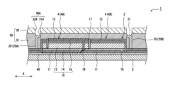
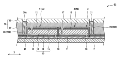
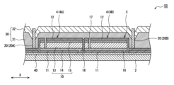
- FIG. 1 shows a schematic cross-sectional structure of a solar cell module 1 according to a first embodiment, cut in the X direction.
- a first direction along the surface of the substrate 2 is defined as the "X direction (shown in FIG. 1)," and a second direction along the surface of the substrate 2 and perpendicular to the X direction is defined as the "Y direction (direction perpendicular to the paper surface of FIG. 1).”
- the solar cell module 1 includes a substrate 2 and a cell 3 provided on the substrate 2.
- the cell 3 is composed of a plurality of unit cells 4 connected in series.
- Each unit cell 4 includes a photoelectric conversion layer 10, a first electrode layer 11, and a second electrode layer 12.
- the solar cell module 1 further includes an extraction electrode layer 20 and a sealing layer 30.
- the extraction electrode layer 20 is an electrode for extracting electrical energy from the cell 3 to the outside of the module, and is provided in an area that does not overlap with the photoelectric conversion layer 10 when the substrate 2 is viewed in a plan view.
- the sealing layer 30 is a layer that sandwiches the cell 3 together with the substrate 2 and prevents water vapor and oxygen from flowing into the module.
- the sealing layer 30 is provided so as to cover the cell 3 (photoelectric conversion layer 10, first electrode layer 11, second electrode layer 12) and the extraction electrode layer 20, and has an opening 30A in the area corresponding to the extraction electrode layer 20.
- the solar cell module 1 may include an inorganic film 40 provided on the substrate 2.
- the inorganic film 40 is interposed between the substrate 2 and the first electrode layer 11.
- the inorganic film 40 may be, for example, an inorganic film of the same type as the barrier layer of the second layer 32 described below.
- the extraction electrode layer 20 is exposed from the opening 30A of the sealing layer 30, and the peripheral portion of the extraction electrode layer 20 is covered by the sealing layer 30. That is, a portion of the surface 21 of the extraction electrode layer 20 facing the side opposite the substrate 2 is exposed from the opening 30A of the sealing layer 30, and the periphery of the exposed portion is covered by the sealing layer 30. In this case, water vapor and oxygen are effectively prevented from flowing into the module from around the extraction electrode layer 20.
- the substrate 2 may be a conductive substrate with an insulating layer formed on its surface, but preferably an insulating substrate is used.
- the substrate 2 is made of a material that is transparent to sunlight with a wavelength of 400 nm or more and 1000 nm or less, and has a low water vapor transmission rate.
- the substrate 2 may be a resin substrate or a glass substrate.
- the thickness of the substrate 2 is, for example, 0.02 mm or more and 3 mm or less. Since the solar cell module 1 has a support 5, it is also possible to use a resin film similar to the barrier film described below as the substrate 2.
- the solar cell module 1 includes a plurality of unit cells 4 connected in series.
- a plurality of unit cells 4 are arranged in the X direction and are continuous in the Y direction perpendicular to the X direction.
- the unit cells 4 in this embodiment are perovskite type cells, and include a first electrode layer 11 provided on the substrate 2, a photoelectric conversion layer 10 provided on the first electrode layer 11, and a second electrode layer 12 provided on the photoelectric conversion layer 10.
- At least one of the substrate 2 and the sealing layer 30 covering the surface of the cell 3 (each unit cell 4) has optical transparency.
- the sealing layer 30 is opaque, and the surface of the substrate 2 becomes the light receiving surface of the module.
- the photoelectric conversion layer 10 includes a light absorbing layer 13, an electron transport layer 14, and a hole transport layer 15, and has a laminated structure in which the electron transport layer 14 and the hole transport layer 15 are arranged to sandwich the light absorbing layer 13 from both sides.
- the electron transport layer 14, the light absorbing layer 13, and the hole transport layer 15 are arranged in this order from the substrate 2 side, except for a portion in which a groove described later is formed.
- the light absorbing layer 22 includes, for example, a perovskite compound represented by a composition formula ABX 3 (wherein A is a monovalent cation, B is a divalent cation, and X is a halogen anion).
- the electron transport layer 14 is made of an n-type semiconductor and is also called an n-layer. Examples of electron transport materials that make up the electron transport layer 14 include anatase-type titanium oxide and tin oxide.
- the hole transport layer 15 is made of a p-type semiconductor and is also called a p-layer.
- the hole transport layer 15 contains a hole transport material that has an oxidation-reduction site. Examples of hole transport materials that make up the hole transport layer 15 include 2,2',7,7'-tetrakis(N,N'-di-p-methoxyphenylamino)-9,9'-spirobifluorene (Spiro-OMeTAD).
- a in the above perovskite compound (ABX 3 ) is a monovalent cation represented by R 1 R 2 R 3 -N-H.
- R 1 and R 2 are H and R 3 is CH 3
- A is methylammonium (CH 3 NH 3 ).
- the functional groups R 1 , R 2 , and R 3 contain at least one element selected from carbon, hydrogen, nitrogen, and oxygen, for example.
- the functional groups R 1 , R 2 , and R 3 contain carbon atoms, the total number of carbon atoms in the functional groups R 1 , R 2 , and R 3 is preferably 4 or less.
- the functional groups R 1 , R 2 , and R 3 may contain a Group 1 element such as Rb or Cs.
- B in ABX 3 is a divalent cation.
- B is, for example, a divalent cation of a transition metal or a group 13 element, a group 14 element, or a group 15 element.
- Specific examples of B include Pb 2+ , Ge 2+ , and Sn 2+ .
- B may contain at least one element selected from Pb 2+ and Sn 2+ , and a part of Pb 2+ and Sn 2+ may be substituted with other elements. Examples of the substitution element include Bi, Sb, In, Ge, and Ni.
- X in ABX 3 is at least one element selected from Cl, Br, and I.
- Each of the A, M, and X sites may be occupied by multiple types of ions.
- Specific examples of perovskite compounds (ABX 3 ) include CH 3 NH 3 PbI 3 , CH 3 CH 2 NH 3 PbI 3 , NH 2 CHNH 2 PbI 3 , CH 3 NH 3 PbBr 3 , CH 3 NH 3 PbCl 3 , CsPbI 3 , and CsPbBr 3 .
- the light absorbing layer 13 made of CH 3 NH 3 PbI 3 is also called a PVSK element.
- the first electrode layer 11 and the second electrode layer 12 are preferably light-transmitting and do not block the entry of light into the photoelectric conversion layer 10.
- the light transmittance of each electrode layer is, for example, 85% or more in the wavelength range of 450 nm to 900 nm.
- the sheet resistance of each electrode layer is preferably 200 ⁇ / ⁇ or less, and may be 50 ⁇ / ⁇ or less.
- a suitable electrode layer is a transparent conductive layer composed of a transparent conductive oxide such as indium tin oxide (ITO) in which a metal oxide such as indium oxide or zinc oxide is doped with tungsten, tin, antimony, or the like.
- the thickness of the transparent conductive layer is, for example, 30 nm to 300 nm.
- Each electrode layer can be formed by a conventional method such as sputtering.
- unit cell 4A two unit cells 4 adjacent to each other in the X direction are shown, with the unit cell 4 on the left side referred to as "unit cell 4A" and the unit cell 4 on the right side referred to as "unit cell 4B".
- the number of unit cells 4 included in the solar cell module 1 is not particularly limited, and may be three or more.
- the second electrode layer 12 of unit cell 4A is electrically connected to the first electrode layer 11 of unit cell 4B.
- the second electrode layer 12 of unit cell 4B is electrically connected to the first electrode layer 11 of a third unit cell 4 adjacent to it in the X direction. In this way, a plurality of unit cells 4 are connected in series along the X direction.
- Grooves 16, 17, and 18 are formed by removing a portion of the layers that make up cell 3, and extend in the Y direction and are formed approximately parallel to each other.
- Each groove can be formed by a conventionally known scribing method or the like.
- Each groove width is, for example, 30 ⁇ m or more and 300 ⁇ m or less.
- Groove 17 is filled with a resin that makes up sealing layer 30 so that no voids are formed within the groove.
- the grooves 16 are grooves that divide the first electrode layer 11 of each unit cell 4.
- the grooves 17 divide the light absorbing layer 13, the hole transport layer 15, and the second electrode layer 12 of each unit cell 4. Note that the grooves 17 only need to divide the second electrode layer 12 of each unit cell 4, and the light absorbing layer 13 and the hole transport layer 15 do not have to be divided by the grooves 17.
- the unit cells 4 are partitioned by the grooves 16 and 17.
- the groove 18 is formed so as to penetrate the hole transport layer 15, the light absorption layer 13, and the electron transport layer 14 to expose the first electrode layer 11 of the unit cell 4B.
- the second electrode layer 12 of the unit cell 4A is formed in the groove 18. This electrically connects the first electrode layer 11 of the unit cell 4B to the second electrode layer 12 of the unit cell 4A.
- the groove 18 functions as a conductive path that connects multiple unit cells 4 in series.
- the cell 3 is manufactured, for example, by the following method.
- a first electrode layer 11 and an electron transport layer 14 are formed in this order on a substrate 2 .
- a portion of the first electrode layer 11 is laser scribed to form a groove 16 .
- On the electron transport layer 14, a light absorbing layer 13 and a hole transport layer 15 are formed in this order.
- the hole transport layer 15, the light absorption layer 13, and a portion of the electron transport layer 14 are subjected to a mechanical scribing process to form grooves 18.
- the second electrode layer 12 is formed on the hole transport layer 15. At this time, the second electrode layer 12 is formed in the groove 18, and the conductive path is formed.
- the second electrode layer 12, the hole transport layer 15, and a portion of the light absorbing layer 13 are subjected to a mechanical scribing process to form grooves 17.
- the light absorption layer 13, the electron transport layer 14, and the hole transport layer 15 can be formed, for example, by applying a solution in which the constituent materials of each layer are dissolved to the surface of the substrate 2.
- These layers may be formed by a meniscus coating method, a spin coating method, or a dispenser.
- the thickness of each layer is not particularly limited, but is, for example, 10 nm or more and 500 nm or less.
- the extraction electrode layer 20 has a structure in which metal layers are stacked, and is provided on the substrate 2 in an area that does not overlap with the photoelectric conversion layer 10 when the substrate 2 is viewed in a plan view. In other words, the extraction electrode layer 20 is provided in an area that does not overlap with the photoelectric conversion layer 10 in the thickness direction of the solar cell module 1.
- the extraction electrode layer 20 includes an extraction electrode layer 20A electrically connected to the first electrode layer 11 of the unit cell 4A, and an extraction electrode layer 20B electrically connected to the second electrode layer 12 of the unit cell 4B.
- the extraction electrode layer 20A is disposed at a first end in the X direction of the substrate 2, and the extraction electrode layer 20B is disposed at a second end in the X direction opposite to the first end.
- the metal layer constituting the extraction electrode layer 20 is composed of, for example, a metal such as aluminum, nickel, copper, or silver, or an alloy of these. Of these, it is preferable to use silver.
- the metal layer may have a single layer structure or a multi-layer structure including a layer of a different metal.
- An example of the thickness of the extraction electrode layer 20 is 10 ⁇ m or more and 100 ⁇ m or less.
- the extraction electrode layer 20 may be formed by printing, sputtering, vapor deposition, or the like, or may be formed by a plating method.
- the sealing layer 30 is a layer that covers the entire cell 3, and prevents water vapor and oxygen from flowing into the module.
- the sealing layer 30 may also have a function of capturing water vapor and the like.
- the sealing layer 30 covers the side surface of the extraction electrode layer 20 along the thickness direction.
- the extraction electrode layer 20 is an electrode for extracting the power generated in the cell 3 to the outside of the module, a part of the surface 21 of the extraction electrode layer 20 facing away from the substrate 2 is exposed and not covered by the sealing layer 30.
- An opening 30A is formed in the sealing layer 30 to expose a part of the surface 21 of the extraction electrode layer 20.
- the sealing layer 30 covers the peripheral portion of the surface 21 of the extraction electrode layer 20.
- the shape of the opening 30A of the sealing layer 30 is not particularly limited, but as an example, it is circular in plan view.
- the opening 30A of the sealing layer 30 is arranged so as to overlap with the surface 21 of the extraction electrode layer 20 in the thickness direction of the module, and the portion where the opening area is smallest is smaller than the surface 21. In this embodiment, the area of the opening 30A is smallest at the portion in contact with the surface 21.
- the sealing layer 30 can be a single-layer structure or a multi-layer structure having three or more layers, but in this embodiment, it has a two-layer structure including a first layer 31 and a second layer 32.
- the first layer 31 has a first opening 31A in a region corresponding to the extraction electrode layer 20.
- the second layer 32 is provided so as to cover the first layer 31, and has a second opening 32A in a region corresponding to the extraction electrode layer 20.
- the first opening 31A and the second opening 32A are arranged to overlap in the thickness direction of the module, forming an opening 30A in the sealing layer 30.
- the first layer 31 is filled in the groove 17 formed in the cell 3, between the cell 3 and the extraction electrode layer 20, etc., and adheres closely to the cell 3 and the extraction electrode layer 20. It is preferable that the first layer 31 adheres closely to the cell 3 without any gaps so that no gaps are formed between the cell 3 and the first layer 31. In this case, the inflow of water vapor and oxygen into the module is suppressed.
- the first layer 31 is preferably made of a resin with low water vapor and oxygen permeability.
- the first layer 31 may contain a moisture absorbing filler.
- the first layer 31, which has the function of capturing moisture, is also called a getter layer.
- the resin constituting the first layer 31 may be any resin that has low water vapor and oxygen permeability and good adhesion to the cells 3, and an example of a suitable resin is an olefin-based polymer.
- An olefin-based polymer is a polymer whose main constituent unit is an olefin-derived unit.
- the first layer 31 is, for example, a layer in which a moisture-absorbing filler is dispersed in an olefin-based polymer.
- the first layer 31 may contain other components other than the olefin-based polymer and the moisture-absorbing filler. Examples of other components include a tackifier, a curing accelerator, an antioxidant, a plasticizer, and a rubber component.
- the olefin polymer is preferably a copolymer of two or more kinds of olefins, or a copolymer of an olefin and a monomer other than an olefin, such as a non-conjugated diene or styrene.
- copolymers include ethylene-non-conjugated diene copolymer, ethylene-propylene copolymer, ethylene-propylene-non-conjugated diene copolymer, ethylene-butene copolymer, propylene-butene copolymer, propylene-butene-non-conjugated diene copolymer, styrene-isobutene copolymer, styrene-isobutene-styrene copolymer, isobutene-isoprene copolymer, etc.
- the olefin polymer preferably has a crosslinked structure, and is obtained by reacting a copolymer containing a first reactive functional group with a copolymer containing a second reactive functional group.
- the reactive functional groups can be selected from the group consisting of epoxy groups, carboxy groups, acid anhydride groups, amino groups, hydroxyl groups, and isocyanate groups, and are used in combinations that react with each other. Specific examples of combinations of reactive functional groups include epoxy groups and carboxy groups, epoxy groups and acid anhydride groups, and carboxy groups and acid anhydride groups.
- moisture-absorbing fillers examples include uncalcined hydrotalcite, semi-calcined hydrotalcite, calcined hydrotalcite, calcium oxide, magnesium oxide, calcined dolomite, calcium hydride, strontium oxide, aluminum oxide, barium oxide, molecular sieves, and silica.
- the thickness of the first layer 31 is, for example, 10 ⁇ m to 100 ⁇ m, and preferably 30 ⁇ m to 70 ⁇ m. If the thickness of the first layer 31 is within this range, good sealing performance and water vapor trapping performance can be ensured.
- the material constituting the first layer 31 is supplied in the form of a film during the manufacturing process of the solar cell module 1, and flows when heated, pressurized, or heated and pressurized, so that it adheres closely to the cells 3 without any gaps, and also fills the grooves of the cells 3.
- the second layer 32 is a layer with low water vapor and oxygen permeability, and is provided to cover the entire first layer 31, suppressing the inflow of water vapor and oxygen into the module.
- the second layer 32 is preferably composed of a resin film having a barrier layer.
- the resin film is composed mainly of resins such as olefin polymers such as polyethylene, polypropylene, and polyvinyl chloride, polyesters such as polyethylene terephthalate, polycarbonate, and polyimide.
- the barrier layer is preferably formed on the inner surface of the resin film, i.e., the surface facing the first layer 31. Examples of barrier layers include inorganic films such as silica vapor deposition films, silicon nitride films, and silicon oxide films.
- the thickness of the second layer 32 is, for example, 20 ⁇ m or more and 150 ⁇ m or less, and preferably 50 ⁇ m or more and 100 ⁇ m or less. Since the thickness of the barrier layer is thinner than that of the resin film, the thickness of the second layer 32 is substantially the same as the thickness of the resin film that constitutes the second layer 32. There is no particular limitation on the relationship between the thicknesses of the first layer 31 and the second layer 32.
- the first layer 31 and the second layer 32 are laminated in this order from the substrate 2 side as described above, and are arranged so that the first opening 31A and the second opening 32A overlap.
- the extraction electrode layer 20 has a portion of its surface 21 exposed from the opening 30A (first opening 31A and second opening 32A) of the sealing layer 30, but the surface 21 is located closer to the substrate 2 than the surface of the sealing layer 30 and is embedded in the sealing layer 30. In this embodiment, the surface 21 of the extraction electrode layer 20 is located closer to the substrate 2 than the interface between the first layer 31 and the second layer 32.
- the first layer 31 preferably covers the peripheral portion of the surface 21 of the extraction electrode layer 20 and adheres closely to the side surface along the thickness direction of the extraction electrode layer 20. In this case, the inflow of water vapor and oxygen into the module is more effectively suppressed.
- the first opening 31A of the first layer 31 is formed smaller than the second opening 32A of the second layer 32.
- the opening 30A of the sealing layer 30 formed by the first opening 31A and the second opening 32A may become gradually smaller as it approaches the surface 21 of the extraction electrode layer 20. In the example shown in FIG. 1, the first opening 31A gradually decreases in diameter toward the surface 21.
- the first layer 31 preferably covers the entire peripheral area of the surface 21. That is, the first layer 31 is in close contact with the surface 21 over the entire peripheral area of the surface 21 so as to surround the portion exposed from the first opening 31A of the surface 21. In this case, the effect of suppressing the inflow of water vapor and oxygen becomes more pronounced.
- the first layer 31 may be disposed over the entire circumference with a substantially constant width from the peripheral area of the surface 21.
- the first layer 31 covers, for example, an area of 10% to 50% of the area of the surface 21.
- the second opening 32A of the second layer 32 is formed to be larger than the surface 21.
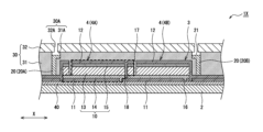
- FIG. 2 is a cross-sectional view of solar cell module 1X, which is a second embodiment
- FIG. 3 is a cross-sectional view of solar cell module 1Y, which is a third embodiment.
- solar cell modules 1X and 1Y are common to solar cell module 1 in that sealing layer 30 has a two-layer structure including first layer 31 and second layer 32, and surface 21 of extraction electrode layer 20 is located closer to substrate 2 than the interface between first layer 31 and second layer 32. That is, extraction electrode layer 20 is embedded in first layer 31. In this case as well, when substrate 2 is viewed in plan from the side on which photoelectric conversion layer 10 is provided, part of surface 21 of extraction electrode layer 20 is exposed from first opening 31A and second opening 32A.
- solar cell modules 1X and 1Y differ from solar cell module 1 in that the second opening 32A of the second layer 32 is smaller than the first opening 31A of the first layer 31.
- the first opening 31A is larger than the second opening 32A.
- the opening area on the outermost surface of solar cell module 1 is smaller, so the amount of water vapor and oxygen flowing into the opening can be reduced.
- the second opening 32A of the second layer 32 is formed smaller than the area of the surface 21 of the extraction electrode layer 20.
- the second layer 32 is disposed on the peripheral portion so as to cover the entire peripheral portion of the surface 21. Since the first layer 31 is interposed between the extraction electrode layer 20 and the second layer 32, the second layer 32 does not contact the surface 21.
- the opening area of the second opening 32A is preferably small enough to not interfere with the extraction of power from the extraction electrode layer 20, and is, for example, 90% or less of the area of the surface 21.
- the first opening 31A of the first layer 31 is formed to be larger than the surface 21, and the peripheral portion of the surface 21 is not covered by the first layer 31.
- the solar cell module 1Y shown in FIG. 3 like the solar cell module 1X, the second opening 32A of the second layer 32 is formed smaller than the area of the surface 21 of the extraction electrode layer 20, and the second layer 32 is disposed on the peripheral portion of the surface 21.
- the solar cell module 1Y differs from the solar cell module 1X in that the first opening 31A of the first layer 31 is formed smaller than the area of the surface 21, and the peripheral portion of the surface 21 is covered by the first layer 31. That is, the order is surface 21 > first opening 31A > second opening 32A, and the peripheral portion of the surface 21 is covered by the first layer 31 and the second layer 32. In this case, the effect of suppressing the inflow of water vapor and oxygen becomes more pronounced.
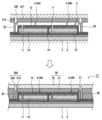
- FIG. 4 to 6 show the cross-sectional structure of a solar cell module during the manufacturing process, cut in the X direction.
- the manufacturing process of the solar cell modules 1, 1X, 1Y includes, for example, the following steps.
- the photoelectric conversion layer 10, the first electrode layer 11, the second electrode layer 12, and the extraction electrode layer 20 can be provided on the substrate 2 by a conventionally known method, as described above.
- FIGS. 4 to 6 are diagrams showing the process of providing the sealing layer 30, each illustrating a different formation method.
- a support 5 is used to support the substrate 2.
- the support 5 is made of a material that is thicker and more rigid than the substrate 2.
- the solar cell module is transported, for example, while placed on the support 5, and each layer is formed on the substrate 2.
- An adhesive layer for adhesion may be provided between the support 5 and the substrate 2.
- FIG 4 shows the manufacturing process of the solar cell module 1.
- the sealing layer 30 is placed on the second electrode layer 12 and the extraction electrode layer 20, a part of the sealing layer 30 is removed to form an opening 30A.
- the opening 30A is formed by a conventionally known scribing method or the like in a region of the sealing layer 30 that corresponds to the extraction electrode layer 20, i.e., a position that overlaps with the extraction electrode layer 20 in the thickness direction of the module.
- the opening 30A is formed so that the extraction electrode layer 20 is exposed through the opening 30A and the peripheral portion of the extraction electrode layer 20 is covered by the sealing layer 30.
- film 31F constituting first layer 31 is placed so as to cover second electrode layer 12 and extraction electrode layer 20, and film 32F constituting second layer 32 is placed on top of that.
- Each film 31F, 32F may be integrated in advance and then supplied onto substrate 2.
- Film 31F placed on substrate 2 is heated, pressurized, or heated and pressurized, thereby adhering film 31F to cell 3, etc.
- material constituting first layer 31 is also filled into groove 17.
- the opening 30A (first opening 31A of the first layer 31) of the sealing layer 30 is formed so that the opening area gradually becomes smaller closer to the surface 21 of the extraction electrode layer 20.
- the first layer 31 covers the entire periphery of the surface 21, but openings may be formed in each film 31F, 32F so that both the first layer 31 and the second layer 32 cover the periphery of the surface 21.
- each opening may be formed so that both the first opening 31A and the second opening 32A are smaller than the area of the surface 21.
- FIG. 5 shows the manufacturing process of the solar cell module 1X.
- a sealing layer 30 having an opening 30A is arranged on the second electrode layer 12 and the extraction electrode layer 20.
- the substrate 2 is viewed in plan from the side on which the photoelectric conversion layer 10 is provided, the extraction electrode layer 20 is exposed through the opening 30A, and the sealing layer 30 is arranged so that the peripheral portion of the extraction electrode layer 20 is covered. That is, in this manufacturing process, films 31F, 32F with openings formed in advance are arranged on the substrate 2. More specifically, the films 31F, 32F are arranged so that the extraction electrode layer 20, the first opening 31A, and the second opening 32A overlap in the thickness direction of the module.
- FIG. 5 shows the manufacturing process for solar cell module 1X, but solar cell modules 1 and 1Y can be manufactured in a similar manner.
- the second opening 32A of the second layer 32 is formed smaller than the first opening 31A of the first layer 31, and the surface 21 of the extraction electrode layer 20 ⁇ first opening 31A > second opening 32A, but the solar cell modules 1 and 1Y can be manufactured by changing the size of each opening.
- FIG. 6 shows the manufacturing process of solar cell module 1Y, but solar cell module 1X can be manufactured in a similar manner.
- a first layer 31 with a first opening 31A formed in advance is provided on the second electrode layer 12 and the extraction electrode layer 20, a second layer 32 is provided on the first layer 31, and then a second opening 32A is formed. That is, this manufacturing process includes the steps of providing a first layer 31 having a first opening 31A in a region corresponding to the extraction electrode layer 20, providing a second layer 32 on the first layer 31, and removing a portion of the second layer 32 to form the second opening 32A.
- the first layer 31 and the second layer 32 are provided and the second opening 32A is formed so that the extraction electrode layer 20 is exposed through the first opening 31A and the second opening 32A and the peripheral portion of the extraction electrode layer 20 is covered by at least one of the first layer 31 and the second layer 32.
- the film 31F is arranged so that the extraction electrode layer 20 and the first opening 31A overlap in the thickness direction of the module, and after the film 32F is laminated on the film 31F, the second opening 32A is formed at a position overlapping the first opening 31A.
- the surface 21 of the extraction electrode layer 20 is located closer to the substrate 2 than the surface of the sealing layer 30, and is embedded in the sealing layer 30.
- the surface 21 of the extraction electrode layer 20 is exposed from the opening 30A of the sealing layer 30. Meanwhile, the surface 21 of the extraction electrode layer 20 is not covered by the first layer 31 and the second layer 32.
- the configurations of the first to third embodiments can be selectively applied to the fourth to sixth embodiments. In this case, the effect of suppressing the inflow of water vapor and oxygen becomes more pronounced.
- the grooves 17 filled with the first layer 31 of the sealing layer 30 are formed so as to gradually widen the further away from the substrate 2.
- the grooves 17 are formed, for example, by removing parts of the photoelectric conversion layer 10, the hole transport layer 15, and the second electrode layer 12 (parts that overlap in the thickness direction of the module), and the opening formed in the hole transport layer 15 is larger than the opening formed in the photoelectric conversion layer 10. Furthermore, the opening in the second electrode layer 12 is larger than the opening in the hole transport layer 15.
- the solar cell module 50 has grooves 17 formed therein that gradually widen the further away from the substrate 2, and the first layer 31 is formed within the grooves 17.
- the grooves 17 may have a width that changes stepwise at the interface between the layers as shown in FIG. 7, or may continuously widen from the photoelectric conversion layer 10 toward the second electrode layer 12.
- the solar cell module 51 of the fifth embodiment fine irregularities are formed on the surface of the second electrode layer 12 that contacts the first layer 31 of the sealing layer 30.
- the contact area between the first layer 31 and the second electrode layer 12 is increased, and the adhesion between the first layer 31 and the second electrode layer 12 is improved.
- gaps are less likely to occur between the first layer 31 and the second electrode layer 12, and the inflow of water vapor and oxygen into the module is effectively suppressed.
- the irregularities may be formed only on the surface of the second electrode layer 12, in the example shown in FIG. 8, the irregularities are formed on the surface of the photoelectric conversion layer 10, and the hole transport layer 15 and the second electrode layer 12 are formed along the irregularities of the photoelectric conversion layer 10, thereby forming the irregularities on the surface of the second electrode layer 12.
- the arithmetic mean roughness Ra of the surface of the second electrode layer 12 is, for example, 1 nm or more and 100 nm or less. If the arithmetic mean roughness Ra is within this range, the effect of improving the adhesion between the first layer 31 and the second electrode layer 12 becomes more significant.
- the arithmetic mean roughness Ra of the surface of the second electrode layer 12 can be measured by cross-sectional TEM.
- the method of forming irregularities on the surface of the photoelectric conversion layer 10 is not particularly limited, but one example is a spin coating method.
- the solar cell module 52 of the sixth embodiment includes a spring electrode 60 as a wiring material electrically connected to the extraction electrode layer 20.
- the spring electrode 60 is disposed in the opening 30A of the sealing layer 30, and one axial end of the spring electrode 60 is in contact with the surface 21 of the extraction electrode layer 20.
- the other axial end of the spring electrode 60 protrudes from the opening 30A and is connected to an external device (not shown).
- the opening 30A may be filled with a sealant 61 that seals the gap between the sealing layer 30 and the spring electrode 60.
- the sealant 61 may be made of a material similar to that of the first layer 31.
- the thickness of the first layer 31 constituting the sealing layer 30 is reduced around the extraction electrode layer 20.
- the extraction electrode layer 20 thicker than the sealing layer 30 and enlarging the opening of the film constituting the first layer 31 to the extent that a gap is created between the extraction electrode layer 20 and the film, the film fills the gap and sinks into the substrate 2.
- the second layer 32 follows the first layer 31, and the surface of the second layer 32 is recessed. As a result, the surface 21 of the extraction electrode layer 20 and its vicinity protrude from the sealing layer 30.
- the sealing layer 30 adheres strongly to the side surface of the extraction electrode layer 20, making it difficult for a gap to form between the extraction electrode layer 20 and the sealing layer 30. As a result, the inflow of water vapor and oxygen into the module is effectively suppressed.
- the solar cell modules of the above embodiments can sufficiently prevent water vapor and oxygen from entering the module.
- the solar cell modules of the above embodiments have excellent sealing performance and can maintain good output performance for a long period of time.
- water vapor and oxygen are effectively prevented from entering the module from around the extraction electrode layer 20.
- the configurations of the first to third embodiments can be selectively applied to the fourth to sixth embodiments, in which case the effect of suppressing the inflow of water vapor and oxygen becomes more pronounced.
- at least one configuration selected from the group consisting of the widening shape of the groove 17 of the fourth embodiment, the surface irregularities of the second electrode layer 12 of the fifth embodiment, and the spring electrode 60 of the sixth embodiment may be applied to the solar cell modules 1, 1X, and 1Y.
- the sealing layer may also be supplied to the solar cell module manufacturing process in the form of a single film containing the barrier layer as an intermediate layer.
- the barrier layer is sandwiched between two resin films, for example.
- the resin film placed on the substrate 2 may be a film having the same function as the film constituting the first layer 31, and the resin film placed on the outside of the barrier layer may be a film having the same function as the film constituting the second layer 32.
Landscapes
- Physics & Mathematics (AREA)
- Electromagnetism (AREA)
- Chemical & Material Sciences (AREA)
- Engineering & Computer Science (AREA)
- Materials Engineering (AREA)
- Photovoltaic Devices (AREA)
Abstract
実施形態の一例である太陽電池モジュール(1)は、基材(2)と、基材(2)上に設けられた第1電極層(11)と、第1電極層(11)上に設けられた光電変換層(10)と、光電変換層(10)上に設けられた第2電極層(12)と、取り出し電極層(20)と、封止層(30)とを備える。封止層(30)は、取り出し電極層(20)に対応した領域に開口(30A)を有する。そして、基材(2)を光電変換層(10)が設けられた面側から平面視したときに、開口(30A)から取り出し電極層(20)が露出し、取り出し電極層(20)の周縁部を封止層(30)が覆っている。
Description
本開示は、太陽電池モジュールおよびその製造方法に関し、より詳しくはガラス基材等の絶縁基材上に光電変換層が成膜された太陽電池モジュールおよびその製造方法に関する。
従来、ガラス基材等の絶縁基材上に光電変換層が形成されてなる太陽電池モジュールが知られている。特許文献1には、基板と、基板上に形成された複数の太陽電池セルと、基板上に形成され、複数の太陽電池セルから電荷を取り出す取り出し電極と、取り出し電極から電荷を収集する取出し配線材と、取り出し配線材を覆う被覆材と、封止材とを備えた太陽電池モジュールが開示されている。
また、特許文献2には、陰極と、陽極と、陰極と陽極との間に配置された光電変換層と、陰極上又は陽極上のいずれか一方に配置された樹脂層とを有する太陽電池セルが開示されている。特許文献2には、光電変換層が、一般式R-M-X3(但し、Rは有機分子、Mは金属原子、Xはハロゲン原子又はカルコゲン原子である。)で表される有機無機ペロブスカイト化合物を含むことが記載されている。
太陽電池セルの光電変換層は、水蒸気、酸素、および光の存在により、出力性能が大きく低下するため、特許文献1,2に記載されるように、光電変換層に水蒸気および酸素が作用しないように光電変換層が封止されている。特に、光電変換層がペロブスカイト素子である場合は、水蒸気および酸素の影響による出力低下が顕著である。また、特許文献1に記載されるように、太陽電池モジュールには、太陽電池セルで発電された電力を外部に取り出すための電極が設けられるが、電極の周囲は他の部分と比べて封止性能が低下し易いため、水蒸気および酸素が電極の周囲から流入することが想定される。
本開示の目的は、モジュール内への水蒸気および酸素の流入を十分に抑制でき、封止性能に優れた太陽電池モジュールを提供することである。
本開示に係る太陽電池モジュールは、基材と、基材上に設けられた第1電極層と、第1電極層上に設けられた光電変換層と、光電変換層上に設けられた第2電極層と、基材上において、当該基材を平面視したときに光電変換層と重ならない領域に設けられた取り出し電極層と、第1電極層、光電変換層、第2電極層、および取り出し電極層を覆うように設けられ、取り出し電極層に対応した領域に開口を有する封止層とを備え、基材を光電変換層が設けられた面側から平面視したときに、開口から取り出し電極層が露出し、取り出し電極層の周縁部を封止層が覆っている。
本開示に係る太陽電池モジュールによれば、モジュール内への水蒸気および酸素の流入を十分に抑制できる。本開示に係る太陽電池モジュールは、封止性能に優れるため、例えば、良好な出力性能を長期にわたって維持できる。
以下、図面を参照しながら、本開示に係る太陽電池モジュールの実施形態の一例について詳細に説明する。なお、以下で説明する複数の実施形態および変形例の各構成要素を選択的に組み合わせてなる形態は本開示の範囲に含まれている。
図1は、第1の実施形態である太陽電池モジュール1をX方向に切断した断面構造を模式的に示す。なお、基材2の表面に沿った第1の方向を「X方向(図1に図示)」、基材2の表面に沿った、X方向と直交する第2の方向を「Y方向(図1の紙面に直交する方向)」とする。図1に示すように、太陽電池モジュール1は、基材2と、基材2上に設けられたセル3とを備える。セル3は、直列に接続された複数のユニットセル4から構成されている。各ユニットセル4は、光電変換層10と、第1電極層11と、第2電極層12とを含む。
太陽電池モジュール1は、さらに、取り出し電極層20と、封止層30とを備える。取り出し電極層20は、セル3から電気エネルギーをモジュールの外部に取り出すための電極であって、基材2を平面視したときに光電変換層10と重ならない領域に設けられている。封止層30は、基材2と共にセル3を挟み、モジュール内に水蒸気および酸素が流入することを抑制するための層である。封止層30は、セル3(光電変換層10、第1電極層11、第2電極層12)および取り出し電極層20を覆うように設けられ、取り出し電極層20に対応する領域に開口30Aを有する。
太陽電池モジュール1は、基材2上に設けられた無機膜40を備えていてもよい。無機膜40は、基材2と第1電極層11の間に介在している。無機膜40には、例えば、後述する第2の層32のバリア層と同種の無機膜を適用できる。
詳しくは後述するが、太陽電池モジュール1では、基材2を光電変換層10が設けられた面側から平面視したときに、封止層30の開口30Aから取り出し電極層20が露出し、取り出し電極層20の周縁部を封止層30が覆った状態となっている。即ち、基材2と反対側を向いた取り出し電極層20の表面21は、その一部が封止層30の開口30Aから露出し、当該露出部の周囲が封止層30により覆われている。この場合、取り出し電極層20の周囲から水蒸気および酸素がモジュール内に流入することが効果的に抑制される。
基材2には、表面に絶縁層が形成された導電性の基材を用いてもよいが、好ましくは絶縁性の基材を用いる。基材2は、例えば、波長400nm以上1000nm以下の太陽光に対する透過性を有し、水蒸気透過率が低い材料で構成される。基材2は、樹脂製の基材であってもよく、ガラス製の基材であってもよい。基材2の厚みは、例えば、0.02mm以上3mm以下である。なお、太陽電池モジュール1は支持体5を備えるため、基材2として、後述するバリアフィルムと同様の樹脂フィルムを用いることも可能である。
太陽電池モジュール1は、上記のように、直列に接続された複数のユニットセル4を含む。ユニットセル4は、X方向に複数配置され、X方向に直交するY方向に連続している。本実施形態のユニットセル4は、ペロブスカイト型のセルであって、基材2上に設けられた第1電極層11と、第1電極層11上に設けられた光電変換層10と、光電変換層10上に設けられた第2電極層12とを含む。なお、セル3(各ユニットセル4)の表面を覆う基材2および封止層30の少なくとも一方が光透過性を有する。この場合、基材2側、又は封止層30側、或いは両側からモジュール内に光が入射し、各ユニットセル4の光電変換層10に吸収されるが、本実施形態では、封止層30が不透明であり、基材2の表面がモジュールの受光面となる。
光電変換層10は、光吸収層13と、電子輸送層14と、正孔輸送層15とを含み、電子輸送層14および正孔輸送層15が光吸収層13を両側から挟むように配置された積層構造を有する。本実施形態の光電変換層10では、後述の溝が形成された部分を除き、基材2側から順に、電子輸送層14、光吸収層13、および正孔輸送層15が配置されている。光吸収層22は、例えば、組成式ABX3(式中、Aは1価のカチオン、Bは2価のカチオン、Xはハロゲンアニオン)で示されるペロブスカイト化合物を含む。
電子輸送層14は、n型半導体により構成され、n層とも呼ばれる。電子輸送層14を構成する電子輸送材料としては、アナターゼ型酸化チタン、酸化錫などが例示される。正孔輸送層15は、p型半導体により構成され、p層とも呼ばれる。正孔輸送層15は、酸化還元部位を有する正孔輸送材料を含む。正孔輸送層15を構成する正孔輸送材料としては、2,2’,7,7’-テトラキス(N,N’-ジ-p-メトキシフェニルアミノ)-9,9’-スピロビフルオレン(Spiro-OMeTAD)などが例示される。
上記ペロブスカイト化合物(ABX3)のAの一例は、R1R2R3-N-Hで表される1価のカチオンである。R1およびR2がH、R3がCH3である場合、Aはメチルアンモニウム(CH3NH3)となる。官能基R1、R2、R3は、例えば、炭素、水素、窒素、および酸素から選択される少なくとも1種の元素を含む。官能基R1、R2、R3が炭素原子を含む場合、官能基R1、R2、R3の炭素数の合計は4以下であることが好ましい。官能基R1、R2、R3は、Rb、Cs等の第1族元素を含んでいてもよい。
ABX3のBは、上記の通り、2価のカチオンである。Bは、例えば、遷移金属又は第13族元素、第14族元素、又は第15族元素の2価のカチオンである。Bの具体例としては、Pb2+、Ge2+、Sn2+が挙げられる。Bは、Pb2+およびSn2+から選択される少なくとも1種を含んでいてもよく、Pb2+、Sn2+の一部が他の元素に置換されていてもよい。置換元素としては、Bi、Sb、In、Ge、Ni等が例示できる。ABX3のXは、Cl、Br、Iから選択される少なくとも1種である。
上記A、M、Xのそれぞれのサイトは、複数種のイオンによって占有されていてもよい。ペロブスカイト化合物(ABX3)の具体例としては、CH3NH3PbI3、CH3CH2NH3PbI3、NH2CHNH2PbI3、CH3NH3PbBr3、CH3NH3PbCl3、CsPbI3、CsPbBr3等が挙げられる。CH3NH3PbI3から構成される光吸収層13は、PVSK素子とも呼ばれる。
第1電極層11および第2電極層12は、光透過性を有し、光電変換層10への光の進入を遮らないことが好ましい。各電極層の光線透過率は、例えば、波長450nm以上900nm以下の範囲において85%以上である。また、各電極層のシート抵抗は、200Ω/□以下が好ましく、50Ω/□以下であってもよい。好適な電極層の一例は、酸化インジウム、酸化亜鉛等の金属酸化物に、タングステン、スズ、アンチモン等がドーピングされた、酸化インジウムスズ(ITO)等の透明導電性酸化物で構成される透明導電層である。透明導電層の厚みは、例えば、30nm以上300nm以下である。各電極層は、スパッタリング等の従来公知の方法により成膜できる。
図1では、X方向に隣り合う2つのユニットセル4を図示し、左側のユニットセル4を「ユニットセル4A」、右側のユニットセル4を「ユニットセル4B」としている。太陽電池モジュール1に含まれるユニットセル4の数は特に限定されず、3個以上であってもよい。図1に示す例では、ユニットセル4Aの第2電極層12が、ユニットセル4Bの第1電極層11と電気的に接続されている。3個以上のユニットセル4が含まれる場合、例えば、ユニットセル4Bの第2電極層12が、X方向に隣り合う第3のユニットセル4の第1電極層11と電気的に接続される。このようにして、複数のユニットセル4がX方向に沿って直列に接続される。
セル3には、溝16,17,18が形成されている。溝16,17,18は、セル3を構成する層の一部を除去して形成され、Y方向に延びて互いに略平行に形成されている。各溝は、従来公知のスクライブ法などにより形成できる。各溝幅は、例えば、30μm以上300μm以下である。溝17には、溝内に空隙が形成されないように、封止層30を構成する樹脂が充填されている。
溝16は、各ユニットセル4の第1電極層11を分割する溝である。溝17は、各ユニットセル4の光吸収層13、正孔輸送層15、および第2電極層12を分割している。なお、溝17は各ユニットセル4の第2電極層12を分割していればよく、光吸収層13と正孔輸送層15は溝17により分割されていなくてもよい。本実施形態では、溝16,17によって各ユニットセル4が区画されているものとする。
溝18は、正孔輸送層15、光吸収層13、および電子輸送層14を貫通して、ユニットセル4Bの第1電極層11を露出させるように形成されている。そして、溝18内にはユニットセル4Aの第2電極層12が形成されている。これにより、ユニットセル4Bの第1電極層11が、ユニットセル4Aの第2電極層12と電気的に接続される。即ち、溝18が複数のユニットセル4を直列に接続する導電パスとして機能する。
セル3は、例えば、以下の方法により製造される。
(1)基材2上に、第1電極層11および電子輸送層14をこの順で形成する。
(2)第1電極層11の一部をレーザースクライブ処理して溝16を形成する。
(3)電子輸送層14上に、光吸収層13および正孔輸送層15をこの順で形成する。
(4)正孔輸送層15、光吸収層13、および電子輸送層14の一部をメカニカルスクライブ処理して溝18を形成する。
(5)正孔輸送層15上に、第2電極層12を形成する。このとき、溝18内に第2電極層12が形成され、上記導電パスが形成される。
(6)第2電極層12、正孔輸送層15、および光吸収層13の一部をメカニカルスクライブ処理して溝17を形成する。
(1)基材2上に、第1電極層11および電子輸送層14をこの順で形成する。
(2)第1電極層11の一部をレーザースクライブ処理して溝16を形成する。
(3)電子輸送層14上に、光吸収層13および正孔輸送層15をこの順で形成する。
(4)正孔輸送層15、光吸収層13、および電子輸送層14の一部をメカニカルスクライブ処理して溝18を形成する。
(5)正孔輸送層15上に、第2電極層12を形成する。このとき、溝18内に第2電極層12が形成され、上記導電パスが形成される。
(6)第2電極層12、正孔輸送層15、および光吸収層13の一部をメカニカルスクライブ処理して溝17を形成する。
光吸収層13、電子輸送層14、および正孔輸送層15は、例えば、各層の構成材料を溶解させた溶液を基材2の表面に塗布することにより成膜できる。これらの層は、メニスカス塗布法、スピンコート法、又はディスペンサーにより成膜されてもよい。各層の厚みは、特に限定されないが、一例としては、10nm以上500nm以下である。
以下、取り出し電極層20および封止層30の構成について詳説する。
取り出し電極層20は、金属層が積層された構造を有し、基材2上において、基材2を平面視したときに光電変換層10と重ならない領域に設けられている。言い換えると、取り出し電極層20は、太陽電池モジュール1の厚み方向に光電変換層10と重ならない領域に設けられている。取り出し電極層20には、ユニットセル4Aの第1電極層11と電気的に接続された取り出し電極層20Aと、ユニットセル4Bの第2電極層12と電気的に接続された取り出し電極層20Bとが含まれている。取り出し電極層20Aは基材2のX方向の第1の端部に配置され、取り出し電極層20Bは当該第1の端部と反対側のX方向の第2の端部に配置されている。
取り出し電極層20を構成する金属層は、例えば、アルミニウム、ニッケル、銅、銀等の金属又はこれらの合金により構成されている。中でも、銀を用いることが好ましい。金属層は、単層構造であってもよく、異種金属層を含む複層構造であってもよい。取り出し電極層20の厚みの一例は、10μm以上100μm以下である。取り出し電極層20は、印刷、スパッタリング、蒸着等により成膜されてもよく、めっき法により成膜されてもよい。
封止層30は、セル3の全体を覆う層であって、水蒸気および酸素がモジュール内に流入することを抑制する。また、封止層30は、水蒸気等を捕捉する機能を有していてもよい。封止層30は、取り出し電極層20の厚み方向に沿った側面を覆っている。一方、取り出し電極層20はセル3で発電された電力をモジュール外に取り出すための電極であるから、基材2と反対側を向いた取り出し電極層20の表面21の一部は、封止層30に覆われず露出している。封止層30には、取り出し電極層20の表面21の一部を露出させる開口30Aが形成されている。
封止層30は、基材2を光電変換層10が設けられた面側から平面視したときに、取り出し電極層20の表面21の周縁部を覆っている。封止層30の開口30Aの形状は特に限定されないが、一例としては、平面視円形状である。封止層30の開口30Aは、モジュールの厚み方向に取り出し電極層20の表面21と重なるように配置され、開口面積が最も小さくなった部分は表面21よりも小さくなっている。本実施形態では、表面21と接する部分で開口30Aの面積が最小となっている。
封止層30は、単層構造、或いは3つ以上の層を有する多層構造とすることも可能であるが、本実施形態では、第1の層31と第2の層32を含む二層構造を有する。第1の層31は、取り出し電極層20に対応した領域に第1の開口31Aを有する。第2の層32は、第1の層31を覆うように設けられ、取り出し電極層20に対応した領域に第2の開口32Aを有する。詳しくは後述するが、第1の開口31Aと第2の開口32Aは、モジュールの厚み方向に重なって配置され、封止層30の開口30Aを形成している。
第1の層31は、セル3に形成された溝17、セル3と取り出し電極層20の間等に充填され、セル3および取り出し電極層20に密着する。第1の層31は、セル3との間に空隙ができないように、セル3と隙間なく密着することが好ましい。この場合、モジュール内への水蒸気および酸素の流入が抑制される。第1の層31は、水蒸気および酸素の透過率が低い樹脂で構成されることが好ましい。第1の層31は、吸湿フィラーを含んでいてもよい。水分を捕捉する機能を有する第1の層31は、ゲッター層とも呼ばれる。
第1の層31を構成する樹脂は、水蒸気および酸素の透過率が低く、セル3に対する密着性が良好な樹脂であればよいが、好適な樹脂の一例としては、オレフィン系ポリマーが挙げられる。オレフィン系ポリマーは、オレフィンに由来する単位を主たる構成単位とするポリマーである。第1の層31は、例えば、オレフィン系ポリマー中に吸湿フィラーが分散した層である。なお、第1の層31は、オレフィン系ポリマーおよび吸湿フィラー以下の他の成分を含んでいてもよい。他の成分としては、粘着付与剤、硬化促進剤、酸化防止剤、可塑剤、ゴム成分等が挙げられる。
オレフィン系ポリマーは、2種以上のオレフィンの共重合体、オレフィンと非共役ジエン、スチレン等のオレフィン以外のモノマーとの共重合体であることが好ましい。共重合体の一例としては、エチレン-非共役ジエン共重合体、エチレン-プロピレン共重合体、エチレン-プロピレン-非共役ジエン共重合体、エチレン-ブテン共重合体、プロピレン-ブテン共重合体、プロピレン-ブテン‐非共役ジエン共重合体、スチレン-イソブテン共重合体、スチレン-イソブテン-スチレン共重合体、イソブテン-イソプレン共重合体等が挙げられる。
オレフィン系ポリマーは、架橋構造を有することが好ましく、第1の反応性官能基を含む共重合体と、第2の反応性官能基を含む共重合体とが反応して得られる。反応性官能基は、エポキシ基、カルボキシ基、酸無水物基、アミノ基、ヒドロキシル基、およびイソシアネート基からなる群より選択でき、互いに反応する組み合わせで用いられる。反応性官能基の組み合わせの具体例としては、エポキシ基とカルボキシ基、エポキシ基と酸無水物基、カルボキシ基と酸無水物基等が挙げられる。
吸湿フィラーの一例としては、未焼成ハイドロタルサイト、半焼成ハイドロタルサイト、焼成ハイドロタルサイト、酸化カルシウム、酸化マグネシウム、焼成ドロマイト、水素化カルシウム、酸化ストロンチウム、酸化アルミニウム、酸化バリウム、モレキュラーシーブ、シリカ等が挙げられる。
第1の層31の厚みは、例えば、10μm以上100μm以下であり、好ましくは30μm以上70μm以下である。第1の層31の厚みが当該範囲内であれば、良好な封止性能、水蒸気等の補足性能を確保できる。第1の層31を構成する材料は、太陽電池モジュール1の製造工程においてフィルム状で供給され、加熱、加圧、又は加熱しながら加圧することにより流動してセル3に隙間なく密着し、セル3の溝内にも充填される。
第2の層32は、水蒸気および酸素の透過率が低い層であって、第1の層31の全体を覆うように設けられ、モジュール内への水蒸気および酸素の流入を抑制する。第2の層32は、バリア層を有する樹脂フィルムにより構成されることが好ましい。樹脂フィルムは、例えば、ポリエチレン、ポリプロピレン、ポリ塩化ビニル等のオレフィン系ポリマー、ポリエチレンテレフタレート等のポリエステル、ポリカーボネート、ポリイミドなどの樹脂を主成分として構成される。バリア層は、樹脂フィルムの内面、即ち第1の層31側に向いた面に形成されることが好ましい。バリア層の一例としては、シリカ蒸着膜、窒化ケイ素膜、酸化ケイ素膜等の無機膜が挙げられる。
第2の層32の厚みは、例えば、20μm以上150μm以下であり、好ましくは50μm以上100μm以下である。なお、バリア層の厚みは樹脂フィルムと比べて薄いことから、第2の層32の厚みは、第2の層32を構成する樹脂フィルムの厚みと実質的に同じである。第1の層31と第2の層32の厚みの関係は特に限定されない。
第1の層31と第2の層32は、上記のように、基材2側からこの順で積層され、第1の開口31Aと第2の開口32Aが重なるように配置される。取り出し電極層20は、その表面21の一部が封止層30の開口30A(第1の開口31Aおよび第2の開口32A)から露出しているが、表面21は封止層30の表面よりも基材2側に位置し、封止層30に埋設された状態である。本実施形態では、取り出し電極層20の表面21が、第1の層31と第2の層32の界面よりも基材2側に位置する。
第1の層31は、取り出し電極層20の表面21の周縁部を覆い、取り出し電極層20の厚み方向に沿った側面に密着していることが好ましい。この場合、モジュール内への水蒸気および酸素の流入がより効果的に抑制される。本実施形態では、第1の層31の第1の開口31Aが、第2の層32の第2の開口32Aより小さく形成されている。第1の開口31Aと第2の開口32Aにより形成される封止層30の開口30Aは、取り出し電極層20の表面21に近づくほど次第に小さくなっていてもよい。図1に示す例では、第1の開口31Aが表面21に向かって次第に縮径している。
第1の層31は、表面21の周縁部の全域を覆っていることが好ましい。即ち、第1の層31は、表面21の第1の開口31Aから露出した部分を囲むように、表面21の周縁部の全周にわたって表面21に密着している。この場合、水蒸気および酸素の流入抑制効果がより顕著になる。第1の層31は、表面21の周縁から略一定の幅で全周にわたって配置されていてもよい。第1の層31は、例えば、表面21の面積の10%以上50%以下の面積を覆っている。本実施形態において、第2の層32の第2の開口32Aは、表面21以上の大きさで形成されている。
図2は第2の実施形態である太陽電池モジュール1Xの断面図、図3は第3の実施形態である太陽電池モジュール1Yの断面図である。
図2および図3に示すように、太陽電池モジュール1X,1Yは、封止層30が第1の層31と第2の層32を含む二層構造を有し、取り出し電極層20の表面21が第1の層31と第2の層32の界面より基材2側に位置する点で、太陽電池モジュール1と共通する。即ち、取り出し電極層20は、第1の層31に埋設された状態である。この場合も、基材2を光電変換層10が設けられた面側から平面視したときに、第1の開口31Aおよび第2の開口32Aから取り出し電極層20の表面21の一部が露出している。
一方、太陽電池モジュール1X,1Yは、第2の層32の第2の開口32Aが、第1の層31の第1の開口31Aよりも小さく形成されている点で、太陽電池モジュール1と異なる。言い換えると、第1の開口31Aが第2の開口32Aよりも広がっている。この場合、太陽電池モジュール1の最外面における開口面積が小さくなるため、開口内に流入する水蒸気および酸素の量を低減できる。
図2に示す太陽電池モジュール1Xでは、第2の層32の第2の開口32Aが、取り出し電極層20の表面21の面積よりも小さく形成されている。そして、第2の層32は、表面21の周縁部を全周にわたって覆うように周縁部上に配置されている。なお、取り出し電極層20と第2の層32の間には第1の層31が介在しているため、第2の層32は表面21に接触していない。第2の開口32Aの開口面積は、取り出し電極層20からの電力の取り出しに支障がない範囲で小さいことが好ましく、一例としては表面21の面積の90%以下である。太陽電池モジュール1Xでは、第1の層31の第1の開口31Aが表面21以上の大きさで形成され、表面21の周縁部は第1の層31により覆われていない。
図3に示す太陽電池モジュール1Yについても、太陽電池モジュール1Xと同様に、第2の層32の第2の開口32Aが取り出し電極層20の表面21の面積よりも小さく形成され、第2の層32が表面21の周縁部上に配置されている。一方、太陽電池モジュール1Yは、第1の層31の第1の開口31Aが表面21の面積よりも小さく形成され、表面21の周縁部が第1の層31により覆われている点で、太陽電池モジュール1Xと異なる。即ち、表面21>第1の開口31A>第2の開口32Aとなり、表面21の周縁部は第1の層31および第2の層32により覆われている。この場合、水蒸気および酸素の流入抑制効果がより顕著になる。
以下、図4~図6を参照しながら、上記構成を備えた太陽電池モジュール1,1X,1Yの製造方法の一例について詳説する。図4~図6は、製造過程の太陽電池モジュールをX方向に切断した断面構造を示す。
太陽電池モジュール1,1X,1Yの製造工程には、例えば、下記の工程が含まれる。
(1)基材2上に、第1電極層11、光電変換層10、および第2電極層12をこの順に設ける工程
(2)基材2上において、基材2を平面視したときに光電変換層10と重ならない領域に取り出し電極層20を設ける工程
(3)第2電極層12および取り出し電極層20上に、封止層30を設ける工程
光電変換層10、第1電極層11、第2電極層12、および取り出し電極層20は、上記のように、従来公知の方法により基材2上に設けることができる。
(1)基材2上に、第1電極層11、光電変換層10、および第2電極層12をこの順に設ける工程
(2)基材2上において、基材2を平面視したときに光電変換層10と重ならない領域に取り出し電極層20を設ける工程
(3)第2電極層12および取り出し電極層20上に、封止層30を設ける工程
光電変換層10、第1電極層11、第2電極層12、および取り出し電極層20は、上記のように、従来公知の方法により基材2上に設けることができる。
図4~図6は、封止層30を設ける工程を示す図であって、それぞれ異なる形成方法を図示している。図4~図6に示す例では、基材2を支持する支持体5が使用されている。支持体5には、基材2よりも厚みが大きく剛性の高い部材が用いられる。太陽電池モジュールは、例えば、支持体5に載せられた状態で、搬送され、基材2上に各層が形成される。支持体5を用いることより、太陽電池モジュールの安定量産が可能となる。支持体5と基材2の間には、接着用の粘着層が設けられていてもよい。
図4は、太陽電池モジュール1の製造工程を示す。図4に示す例では、第2電極層12および取り出し電極層20上に封止層30を配置した後、封止層30の一部を除去して開口30Aを形成している。開口30Aは、従来公知のスクライブ法などにより、封止層30の取り出し電極層20に対応する領域、即ちモジュールの厚み方向に取り出し電極層20と重なる位置に形成される。基材2を光電変換層10が設けられた面側から平面視したときに、取り出し電極層20が開口30Aを介して露出し、封止層30により取り出し電極層20の周縁部が覆われるように開口30Aを形成する。
図4に示す例では、第2電極層12および取り出し電極層20を覆うように、第1の層31を構成するフィルム31Fを配置し、さらにその上に第2の層32を構成するフィルム32Fを配置する。各フィルム31F,32Fは予め一体化された後、基材2上に供給されてもよい。基材2上に配置されたフィルム31Fを加熱、加圧、又は加熱しながら加圧することにより、フィルム31Fをセル3等に密着させる。このとき、溝17内にも第1の層31を構成する材料が充填される。
図4に示す例では、取り出し電極層20の表面21に近づくほど開口面積が次第に小さくなるように、封止層30の開口30A(第1の層31の第1の開口31A)が形成される。第1の層31は、表面21の周縁部を全周にわたって覆っているが、第1の層31と第2の層32の両方が表面21の周縁部を覆う状態となるように、各フィルム31F,32Fに開口を形成してもよい。即ち、第1の開口31Aと第2の開口32Aの両方が、表面21の面積よりも小さくなるように各開口を形成してもよい。
図5は、太陽電池モジュール1Xの製造工程を示す。図5に示す例では、第2電極層12および取り出し電極層20上に、開口30Aを有する封止層30を配置している。この場合、基材2を光電変換層10が設けられた面側から平面視したときに、取り出し電極層20が開口30Aを介して露出し、取り出し電極層20の周縁部が覆われるように封止層30が配置される。即ち、この製造工程では、予め開口が形成されたフィルム31F,32Fを基材2上に配置する。より詳しくは、モジュールの厚み方向に取り出し電極層20、第1の開口31A、および第2の開口32Aが重なるようにフィルム31F,32Fを配置する。
図5は、太陽電池モジュール1Xの製造工程を示すが、同様の方法で太陽電池モジュール1,1Yを製造可能である。図5に示す例では、第2の層32の第2の開口32Aが、第1の層31の第1の開口31Aよりも小さく形成され、取り出し電極層20の表面21≧第1の開口31A>第2の開口32Aとなっているが、各開口の大きさを変更することで、太陽電池モジュール1,1Yを製造できる。
図6は、太陽電池モジュール1Yの製造工程を示すが、同様の方法で太陽電池モジュール1Xを製造可能である。図6に示す例では、第2電極層12および取り出し電極層20上に、予め第1の開口31Aが形成された第1の層31を設け、第1の層31上に第2の層32を設けた後、第2の開口32Aを形成している。即ち、この製造工程には、取り出し電極層20に対応した領域に第1の開口31Aを有する第1の層31を設ける工程と、第1の層31上に第2の層32を設ける工程と、第2の層32の一部を除去して第2の開口32Aを形成する工程とが含まれる。
図6に示す例では、基材2を光電変換層10が設けられた面側から平面視したときに、取り出し電極層20が第1の開口31Aおよび第2の開口32Aを介して露出し、第1の層31および第2の層32の少なくとも一方により取り出し電極層20の周縁部が覆われるように、第1の層31および第2の層32を設け、第2の開口32Aを形成する。この製造工程では、モジュールの厚み方向に取り出し電極層20と第1の開口31Aが重なるようにフィルム31Fを配置し、フィルム31F上にフィルム32Fを積層した後、第1の開口31Aと重なる位置に第2の開口32Aを形成する。
以下、図7~図10を参照しながら、太陽電池モジュールの他の実施形態について説明する。以下では、上記実施形態との相違点について説明する。
図7~図9に例示する第4~第6の実施形態では、上記実施形態と同様に、取り出し電極層20の表面21が封止層30の表面よりも基材2側に位置し、封止層30に埋設されている。また、取り出し電極層20の表面21は封止層30の開口30Aから露出している。一方、取り出し電極層20の表面21は第1の層31および第2の層32により覆われていない。但し、第4~第6の実施形態に上記第1~第3の実施形態の構成を選択的に適用可能である。この場合、水蒸気および酸素の流入抑制効果がより顕著になる。
図7に示すように、第4の実施形態である太陽電池モジュール50では、封止層30の第1の層31が充填される溝17が、基材2から離れるほど次第に拡幅するように形成されている。溝17は、例えば、光電変換層10、正孔輸送層15、および第2電極層12の一部(モジュールの厚み方向に重なる部分)を除去することにより形成されるが、光電変換層10に形成された開口よりも、正孔輸送層15に形成された開口が大きくなっている。さらに、正孔輸送層15の開口よりも、第2電極層12の開口が大きくなっている。
太陽電池モジュール50には、上記のように、基材2から離れるほど次第に拡幅した溝17が形成され、溝17内には、第1の層31が形成されている。溝17は、図7に示すように各層の界面で段階的に幅が変化していてもよく、光電変換層10から第2電極層12に向かって連続的に拡幅していてもよい。このような溝17を有することにより、溝内に第1の層31の構成材料が充填され易くなり、溝内に空隙が形成され難くなる。その結果、モジュール内への水蒸気および酸素の流入が効果的に抑制される。
図8に示すように、第5の実施形態である太陽電池モジュール51では、封止層30の第1の層31と接する第2電極層12の表面に微細な凹凸が形成されている。この場合、第1の層31と第2電極層12の接触面積が大きくなり、第1の層31と第2電極層12の密着性が向上する。その結果、第1の層31と第2電極層12の間に空隙が発生し難くなり、モジュール内への水蒸気および酸素の流入が効果的に抑制される。凹凸は第2電極層12の表面のみに形成されてもよいが、図8に示す例では、光電変換層10の表面に凹凸が形成され、光電変換層10の凹凸に沿って正孔輸送層15および第2電極層12が成膜されることで、第2電極層12の表面に凹凸が形成されている。
第2電極層12の表面の算術平均粗さRaは、例えば、1nm以上100nm以下である。算術平均粗さRaが当該範囲内であれば、第1の層31と第2電極層12の密着性の改善効果がより顕著になる。第2電極層12の表面の算術平均粗さRaは、断面TEMにより測定できる。光電変換層10の表面に凹凸を形成する方法は特に限定されないが、一例としては、スピンコート法が挙げられる。
図9に示すように、第6の実施形態である太陽電池モジュール52は、取り出し電極層20と電気的に接続された配線材として、スプリング電極60を備える。スプリング電極60は、封止層30の開口30A内に配置され、軸方向一端部が取り出し電極層20の表面21に接触している。スプリング電極60の軸方向他端部は、開口30Aから突出し、図示しない外部装置に接続される。開口30Aには、封止層30とスプリング電極60との隙間を塞ぐ封止材61が充填されていてもよい。封止材61には、例えば、第1の層31の構成材料と同様の材料を用いることができる。
図10に示すように、第7の実施形態である太陽電池モジュール53では、取り出し電極層20の周囲において、封止層30を構成する第1の層31の厚みが小さくなっている。取り出し電極層20を封止層30よりも厚く形成し、かつ第1の層31を構成するフィルムの開口を取り出し電極層20との間に隙間が生じる程度に大きくすることにより、フィルムが当該隙間に充填されて基材2側に沈み込む。そして、取り出し電極層20の周囲において、第2の層32が第1の層31に追従し、第2の層32の表面が凹んだ状態となる。このため、取り出し電極層20の表面21およびその近傍は、封止層30から突出している。
太陽電池モジュール53によれば、封止層30が取り出し電極層20の側面に強く密着し、取り出し電極層20と封止層30の間に空隙が形成され難くなる。その結果、モジュール内への水蒸気および酸素の流入が効果的に抑制される。
以上のように、上記各実施形態の太陽電池モジュールによれば、モジュール内への水蒸気および酸素の流入を十分に抑制できる。上記各実施形態の太陽電池モジュールは、封止性能に優れるため、良好な出力性能を長期にわたって維持できる。特に、第1~第3実施形態の太陽電池モジュール1,1X,1Yのように、基材2を光電変換層10が設けられた面側から平面視したときに、取り出し電極層20の周縁部が封止層30により覆われている場合、取り出し電極層20の周囲から水蒸気および酸素がモジュール内に流入することが効果的に抑制される。
なお、上記実施形態は本開示の目的を損なわない範囲で適宜設計変更が可能である。上記のように、第4~第6の実施形態に第1~第3の実施形態の構成を選択的に適用でき、この場合、水蒸気および酸素の流入抑制効果がより顕著になる。換言すると、太陽電池モジュール1,1X,1Yに、第4の実施形態の溝17の拡幅形状、第5の実施形態の第2電極層12の表面凹凸、および第6の実施形態のスプリング電極60からなる群より選択される少なくとも1つの構成を適用してもよい。
また、封止層は、上記バリア層を中間層として含む1枚のフィルムの状態で太陽電池モジュールの製造工程に供給されてもよい。バリア層は、例えば、2枚の樹脂フィルムで挟まれている。基材2に配置される樹脂フィルムには、上記第1の層31を構成するフィルムと同様の機能を有するフィルムを適用でき、バリア層の外側に配置される樹脂フィルムには、上記第2の層32を構成するフィルムと同様の機能を有するフィルムを適用できる。
1,1X,1Y,50,51,52,53 太陽電池モジュール、2 基材、3 セル、4,4A,4B ユニットセル、5 支持体、10 光電変換層、11 第1電極層、12 第2電極層、13 光吸収層、14 電子輸送層、15 正孔輸送層、16,17,18 溝、20,21,20B 取り出し電極層、21 表面、30 封止層、30A 開口、31 第1の層、31A 第1の開口、32 第2の層、32A 第2の開口、40 無機膜、60 スプリング電極、61 封止材
Claims (7)
- 基材と、
前記基材上に設けられた第1電極層と、
前記第1電極層上に設けられた光電変換層と、
前記光電変換層上に設けられた第2電極層と、
前記基材上において、当該基材を平面視したときに前記光電変換層と重ならない領域に設けられた取り出し電極層と、
前記第1電極層、前記光電変換層、前記第2電極層、および前記取り出し電極層を覆うように設けられ、前記取り出し電極層に対応した領域に開口を有する封止層と、
を備え、
前記基材を前記光電変換層が設けられた面側から平面視したときに、前記開口から前記取り出し電極層が露出し、前記取り出し電極層の周縁部を前記封止層が覆っている、太陽電池モジュール。 - 前記封止層は、前記取り出し電極層に対応した領域に第1の開口を有する第1の層と、前記第1の層を覆うように設けられ、前記取り出し電極層に対応した領域に第2の開口を有する第2の層とを含み、
前記基材を前記光電変換層が設けられた面側から平面視したときに、前記第1および前記第2の開口から前記取り出し電極層が露出し、
前記第2の開口は、前記第1の開口より小さく形成されている、請求項1に記載の太陽電池モジュール。 - 前記基材を前記光電変換層が設けられた面側から平面視したときに、前記取り出し電極層の周縁部を前記第1および前記第2の層が覆っている、請求項2に記載の太陽電池モジュール。
- 前記光電変換層は、光吸収層と、電子輸送層と、正孔輸送層とを有し、
前記光吸収層は、ペロブスカイト化合物を含む、請求項1~3のいずれか一項に記載の太陽電池モジュール。 - 基材上に第1電極層、光電変換層、および第2電極層をこの順に設ける工程と、
前記基材上において、当該基材を平面視したときに前記光電変換層と重ならない領域に取り出し電極層を設ける工程と、
前記第2電極層および前記取り出し電極層上に、開口を有する封止層を設ける工程と、
を含み、
前記基材を前記光電変換層が設けられた面側から平面視したときに、前記取り出し電極が前記開口を介して露出し、前記取り出し電極層の周縁部が覆われるように前記封止層を設ける、太陽電池モジュールの製造方法 - 基材上に第1電極層、光電変換層、および第2電極層をこの順に設ける工程と、
前記基材上において、当該基材を平面視したときに前記光電変換層と重ならない領域に取り出し電極層を設ける工程と、
前記第2電極層および前記取り出し電極層上に、封止層を設ける工程と、
前記封止層の一部を除去して開口を形成する工程と、
を含み、
前記基材を前記光電変換層が設けられた面側から平面視したときに、前記取り出し電極が前記開口を介して露出し、前記封止層により前記取り出し電極層の周縁部が覆われるように、前記封止層に前記開口を形成する、太陽電池モジュールの製造方法。 - 基材上に第1電極層、光電変換層、および第2電極層をこの順に設ける工程と、
前記基材上において、当該基材を平面視したときに前記光電変換層と重ならない領域に取り出し電極層を設ける工程と、
前記第2電極層および前記取り出し電極層上に第1の封止層を設ける工程であって、前記取り出し電極層に対応した領域に第1の開口を有する第1の封止層を設ける工程と、
前記第1の封止層上に第2の封止層を設ける工程と、
前記第2の封止層の一部を除去して第2の開口を形成する工程と、
を含み、
前記基材を前記光電変換層が設けられた面側から平面視したときに、前記取り出し電極が前記第1および前記第2の開口を介して露出し、前記第1および前記第2の封止層の少なくとも一方により前記取り出し電極層の周縁部が覆われるように、前記第1および前記第2の封止層を設け、前記第2の開口を形成する、太陽電池モジュールの製造方法。
Applications Claiming Priority (2)
| Application Number | Priority Date | Filing Date | Title |
|---|---|---|---|
| JP2022158254A JP2024051878A (ja) | 2022-09-30 | 2022-09-30 | 太陽電池モジュールおよび太陽電池モジュールの製造方法 |
| JP2022-158254 | 2022-09-30 |
Publications (1)
| Publication Number | Publication Date |
|---|---|
| WO2024070498A1 true WO2024070498A1 (ja) | 2024-04-04 |
Family
ID=90477210
Family Applications (1)
| Application Number | Title | Priority Date | Filing Date |
|---|---|---|---|
| PCT/JP2023/032073 WO2024070498A1 (ja) | 2022-09-30 | 2023-09-01 | 太陽電池モジュールおよび太陽電池モジュールの製造方法 |
Country Status (2)
| Country | Link |
|---|---|
| JP (1) | JP2024051878A (ja) |
| WO (1) | WO2024070498A1 (ja) |
Citations (7)
| Publication number | Priority date | Publication date | Assignee | Title |
|---|---|---|---|---|
| JP2005243440A (ja) * | 2004-02-26 | 2005-09-08 | Hitachi Maxell Ltd | 光電変換素子 |
| CN205542904U (zh) * | 2016-02-26 | 2016-08-31 | 景德镇陶瓷学院 | 一种用于钙钛矿太阳能电池的非接触式封装器件 |
| WO2018052032A1 (ja) * | 2016-09-14 | 2018-03-22 | 積水化学工業株式会社 | フレキシブル太陽電池 |
| JP2018113437A (ja) * | 2017-01-12 | 2018-07-19 | 株式会社リコー | 光電変換素子及び太陽電池 |
| JP2018147956A (ja) * | 2017-03-02 | 2018-09-20 | 積水化学工業株式会社 | 太陽電池 |
| WO2019065430A1 (ja) * | 2017-09-29 | 2019-04-04 | 積水化学工業株式会社 | 太陽電池モジュール、および太陽電池モジュールの製造方法 |
| CN112582549A (zh) * | 2020-12-28 | 2021-03-30 | 厦门大学 | 一种薄型无溶剂钙钛矿太阳能电池封装方法 |
-
2022
- 2022-09-30 JP JP2022158254A patent/JP2024051878A/ja active Pending
-
2023
- 2023-09-01 WO PCT/JP2023/032073 patent/WO2024070498A1/ja unknown
Patent Citations (7)
| Publication number | Priority date | Publication date | Assignee | Title |
|---|---|---|---|---|
| JP2005243440A (ja) * | 2004-02-26 | 2005-09-08 | Hitachi Maxell Ltd | 光電変換素子 |
| CN205542904U (zh) * | 2016-02-26 | 2016-08-31 | 景德镇陶瓷学院 | 一种用于钙钛矿太阳能电池的非接触式封装器件 |
| WO2018052032A1 (ja) * | 2016-09-14 | 2018-03-22 | 積水化学工業株式会社 | フレキシブル太陽電池 |
| JP2018113437A (ja) * | 2017-01-12 | 2018-07-19 | 株式会社リコー | 光電変換素子及び太陽電池 |
| JP2018147956A (ja) * | 2017-03-02 | 2018-09-20 | 積水化学工業株式会社 | 太陽電池 |
| WO2019065430A1 (ja) * | 2017-09-29 | 2019-04-04 | 積水化学工業株式会社 | 太陽電池モジュール、および太陽電池モジュールの製造方法 |
| CN112582549A (zh) * | 2020-12-28 | 2021-03-30 | 厦门大学 | 一种薄型无溶剂钙钛矿太阳能电池封装方法 |
Also Published As
| Publication number | Publication date |
|---|---|
| JP2024051878A (ja) | 2024-04-11 |
Similar Documents
| Publication | Publication Date | Title |
|---|---|---|
| JP6640174B2 (ja) | 太陽電池及びその製造方法 | |
| US10644171B2 (en) | Solar cell | |
| JP6224646B2 (ja) | 太陽電池及びその製造方法 | |
| JP6050409B2 (ja) | 太陽電池 | |
| KR101210168B1 (ko) | 태양광 발전장치 및 이의 제조방법 | |
| US8809676B2 (en) | Thin film solar cell and method of manufacturing the same | |
| JP2017028292A (ja) | 太陽電池 | |
| JP2012015269A (ja) | 太陽電池モジュール | |
| JP2020092267A (ja) | 太陽電池とその製造方法及び太陽電池パネル | |
| US20090320895A1 (en) | Solar cell module | |
| WO2024070498A1 (ja) | 太陽電池モジュールおよび太陽電池モジュールの製造方法 | |
| KR101154654B1 (ko) | 태양광 발전장치 및 이의 제조방법 | |
| JP2009099883A (ja) | 薄膜太陽電池モジュール | |
| US9087953B2 (en) | Solar cell module and method for manufacturing the same | |
| AU2018101195A4 (en) | Solar cell and manufacturing method therefor | |
| KR101114079B1 (ko) | 태양광 발전장치 및 이의 제조방법 | |
| JP4568531B2 (ja) | 集積型太陽電池及び集積型太陽電池の製造方法 | |
| US9076900B2 (en) | Solar cell module and solar cell | |
| US20150027532A1 (en) | Solar cell, solar cell module and method of manufacturing solar cell | |
| US9391219B2 (en) | Photovoltaic apparatus | |
| JP2013527622A (ja) | 太陽電池モジュールおよびそのための製造方法 | |
| WO2023224005A1 (ja) | 太陽電池モジュールおよび太陽電池モジュールの製造方法 | |
| US9972728B2 (en) | Solar cell, solar cell module, and method for manufacturing solar cell | |
| US20220077412A1 (en) | Solar cell module | |
| US20230129154A1 (en) | Solar cell module |
Legal Events
| Date | Code | Title | Description |
|---|---|---|---|
| 121 | Ep: the epo has been informed by wipo that ep was designated in this application |
Ref document number: 23871738 Country of ref document: EP Kind code of ref document: A1 |