WO2024062684A1 - 積層セラミックコンデンサ - Google Patents
積層セラミックコンデンサ Download PDFInfo
- Publication number
- WO2024062684A1 WO2024062684A1 PCT/JP2023/019376 JP2023019376W WO2024062684A1 WO 2024062684 A1 WO2024062684 A1 WO 2024062684A1 JP 2023019376 W JP2023019376 W JP 2023019376W WO 2024062684 A1 WO2024062684 A1 WO 2024062684A1
- Authority
- WO
- WIPO (PCT)
- Prior art keywords
- main surface
- laminate
- ceramic capacitor
- multilayer ceramic
- external electrode
- Prior art date
- Legal status (The legal status is an assumption and is not a legal conclusion. Google has not performed a legal analysis and makes no representation as to the accuracy of the status listed.)
- Ceased
Links
Images


Classifications
-
- H—ELECTRICITY
- H01—ELECTRIC ELEMENTS
- H01G—CAPACITORS; CAPACITORS, RECTIFIERS, DETECTORS, SWITCHING DEVICES, LIGHT-SENSITIVE OR TEMPERATURE-SENSITIVE DEVICES OF THE ELECTROLYTIC TYPE
- H01G4/00—Fixed capacitors; Processes of their manufacture
- H01G4/002—Details
- H01G4/228—Terminals
- H01G4/232—Terminals electrically connecting two or more layers of a stacked or rolled capacitor
-
- H—ELECTRICITY
- H01—ELECTRIC ELEMENTS
- H01G—CAPACITORS; CAPACITORS, RECTIFIERS, DETECTORS, SWITCHING DEVICES, LIGHT-SENSITIVE OR TEMPERATURE-SENSITIVE DEVICES OF THE ELECTROLYTIC TYPE
- H01G4/00—Fixed capacitors; Processes of their manufacture
- H01G4/002—Details
- H01G4/224—Housing; Encapsulation
-
- H—ELECTRICITY
- H01—ELECTRIC ELEMENTS
- H01G—CAPACITORS; CAPACITORS, RECTIFIERS, DETECTORS, SWITCHING DEVICES, LIGHT-SENSITIVE OR TEMPERATURE-SENSITIVE DEVICES OF THE ELECTROLYTIC TYPE
- H01G2/00—Details of capacitors not covered by a single one of groups H01G4/00-H01G11/00
- H01G2/02—Mountings
- H01G2/06—Mountings specially adapted for mounting on a printed-circuit support
-
- H—ELECTRICITY
- H01—ELECTRIC ELEMENTS
- H01G—CAPACITORS; CAPACITORS, RECTIFIERS, DETECTORS, SWITCHING DEVICES, LIGHT-SENSITIVE OR TEMPERATURE-SENSITIVE DEVICES OF THE ELECTROLYTIC TYPE
- H01G4/00—Fixed capacitors; Processes of their manufacture
- H01G4/002—Details
- H01G4/005—Electrodes
- H01G4/012—Form of non-self-supporting electrodes
-
- H—ELECTRICITY
- H01—ELECTRIC ELEMENTS
- H01G—CAPACITORS; CAPACITORS, RECTIFIERS, DETECTORS, SWITCHING DEVICES, LIGHT-SENSITIVE OR TEMPERATURE-SENSITIVE DEVICES OF THE ELECTROLYTIC TYPE
- H01G4/00—Fixed capacitors; Processes of their manufacture
- H01G4/002—Details
- H01G4/018—Dielectrics
- H01G4/06—Solid dielectrics
- H01G4/08—Inorganic dielectrics
- H01G4/12—Ceramic dielectrics
- H01G4/1209—Ceramic dielectrics characterised by the ceramic dielectric material
-
- H—ELECTRICITY
- H01—ELECTRIC ELEMENTS
- H01G—CAPACITORS; CAPACITORS, RECTIFIERS, DETECTORS, SWITCHING DEVICES, LIGHT-SENSITIVE OR TEMPERATURE-SENSITIVE DEVICES OF THE ELECTROLYTIC TYPE
- H01G4/00—Fixed capacitors; Processes of their manufacture
- H01G4/002—Details
- H01G4/228—Terminals
- H01G4/232—Terminals electrically connecting two or more layers of a stacked or rolled capacitor
- H01G4/2325—Terminals electrically connecting two or more layers of a stacked or rolled capacitor characterised by the material of the terminals
-
- H—ELECTRICITY
- H01—ELECTRIC ELEMENTS
- H01G—CAPACITORS; CAPACITORS, RECTIFIERS, DETECTORS, SWITCHING DEVICES, LIGHT-SENSITIVE OR TEMPERATURE-SENSITIVE DEVICES OF THE ELECTROLYTIC TYPE
- H01G4/00—Fixed capacitors; Processes of their manufacture
- H01G4/30—Stacked capacitors
-
- Y—GENERAL TAGGING OF NEW TECHNOLOGICAL DEVELOPMENTS; GENERAL TAGGING OF CROSS-SECTIONAL TECHNOLOGIES SPANNING OVER SEVERAL SECTIONS OF THE IPC; TECHNICAL SUBJECTS COVERED BY FORMER USPC CROSS-REFERENCE ART COLLECTIONS [XRACs] AND DIGESTS
- Y02—TECHNOLOGIES OR APPLICATIONS FOR MITIGATION OR ADAPTATION AGAINST CLIMATE CHANGE
- Y02E—REDUCTION OF GREENHOUSE GAS [GHG] EMISSIONS, RELATED TO ENERGY GENERATION, TRANSMISSION OR DISTRIBUTION
- Y02E60/00—Enabling technologies; Technologies with a potential or indirect contribution to GHG emissions mitigation
- Y02E60/13—Energy storage using capacitors
Definitions
- the present invention relates to a multilayer ceramic capacitor.
- the objective of the present invention is to provide a multilayer ceramic capacitor that can suppress a decrease in strength against external stress even when made thin.
- a multilayer ceramic capacitor according to the present invention is a laminate in which a plurality of dielectric layers made of a ceramic material and a plurality of internal electrode layers are stacked, and the multilayer ceramic capacitor has a first main surface and a second main surface facing each other in the stacking direction.
- a laminate having a surface, two side surfaces facing each other in a width direction intersecting the lamination direction, and two end faces facing each other in a length direction intersecting the lamination direction and the width direction;
- the device includes a plurality of external electrodes disposed on at least the second main surface, and a stress suppression film that suppresses stress applied to the laminate and the plurality of external electrodes.
- the stress suppressing film is made of an insulating material, and extends along the first main surface and the two end surfaces so as to cover the laminate and the plurality of external electrodes. , or extending along the first main surface and the two side surfaces. An end portion of the stress suppressing film protrudes from the outermost surface of the plurality of external electrodes on the second main surface side.
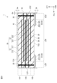
- FIG. 1 is a perspective view showing a multilayer ceramic capacitor according to the present embodiment.
- FIG. 2 is a cross-sectional view (LT cross-section) taken along line II-II of the multilayer ceramic capacitor shown in FIG. 1.
- FIG. 2 is a cross-sectional view (WT cross-section) taken along line III-III of the multilayer ceramic capacitor shown in FIG. 1.
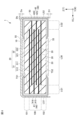
- FIG. 3 is a perspective view showing a multilayer ceramic capacitor according to a modification of the present embodiment.
- 5 is a cross-sectional view (LT cross-section) taken along the line V-V of the multilayer ceramic capacitor shown in FIG. 4.
- FIG. 5 is a cross-sectional view (WT cross-section) taken along the line VI-VI of the multilayer ceramic capacitor shown in FIG. 4.
- FIG. 3 is a perspective view showing a multilayer ceramic capacitor according to a modification of the present embodiment.
- 8 is a cross-sectional view (LT cross-section) of the multilayer ceramic capacitor shown in FIG. 7 taken along line VIII-VIII.
- 8 is a cross-sectional view (WT cross-section) taken along line IX-IX of the multilayer ceramic capacitor shown in FIG. 7.
- FIG. 11 is a perspective view showing a multilayer ceramic capacitor according to a modified example of the present embodiment.
- FIG. 3 is a perspective view showing a multilayer ceramic capacitor according to a modification of the present embodiment.
- FIG. 3 is a perspective view showing a multilayer ceramic capacitor according to a modification of the present embodiment.
- FIG. 1 is a perspective view showing the multilayer ceramic capacitor according to the present embodiment
- FIG. 2 is a sectional view taken along the line II-II of the multilayer ceramic capacitor shown in FIG. 1
- FIG. 3 is a perspective view showing the multilayer ceramic capacitor shown in FIG. FIG. 3 is a sectional view taken along the line III-III of the capacitor.
- a multilayer ceramic capacitor 1 shown in FIGS. 1 to 3 includes a multilayer body 10, an external electrode 40, and a stress suppressing film 50.
- External electrode 40 includes a first external electrode 41 and a second external electrode 42 .
- FIGS. 1 to 3 An XYZ orthogonal coordinate system is shown in FIGS. 1 to 3 and the drawings described below.
- the X direction is the length direction L of the multilayer ceramic capacitor 1 and the laminate 10
- the Y direction is the width direction W of the multilayer ceramic capacitor 1 and the laminate 10
- the Z direction is the length direction L of the multilayer ceramic capacitor 1 and the laminate 10.
- the direction is T. Accordingly, the cross section shown in FIG. 2 is also referred to as the LT cross section, and the cross section shown in FIG. 3 is also referred to as the WT cross section.
- the length direction L, the width direction W, and the lamination direction T are not necessarily orthogonal to each other, but may be intersecting with each other.
- the laminate 10 has a substantially rectangular parallelepiped shape, and has a first main surface TS1 and a second main surface TS2 facing in the stacking direction T, and a first side surface WS1 and a second side surface WS2 facing in the width direction W. , has a first end surface LS1 and a second end surface LS2 facing each other in the length direction L.
- a corner is a part where three sides of the laminate 10 intersect, and a ridgeline is a part where two sides of the laminate 10 intersect.
- the stacked body 10 includes a plurality of dielectric layers 20 and a plurality of internal electrode layers 30 stacked in the stacking direction T. Further, in the stacking direction T, the stacked body 10 includes an inner layer section 100, and a first outer layer section 101 and a second outer layer section 102 that are arranged to sandwich the inner layer section 100.
- the inner layer section 100 includes a portion of the plurality of dielectric layers 20 and the plurality of internal electrode layers 30. In the inner layer section 100, a plurality of internal electrode layers 30 are arranged facing each other with the dielectric layer 20 in between.
- the inner layer portion 100 is a portion that generates capacitance and essentially functions as a capacitor.
- the first outer layer part 101 is arranged on the first main surface TS1 side of the laminate 10, and the second outer layer part 102 is arranged on the second main surface TS2 side of the laminate 10. More specifically, the first outer layer portion 101 is arranged between the internal electrode layer 30 closest to the first main surface TS1 among the plurality of internal electrode layers 30 and the first main surface TS1. , the second outer layer portion 102 is arranged between the internal electrode layer 30 closest to the second main surface TS2 among the plurality of internal electrode layers 30 and the second main surface TS2.
- the first outer layer section 101 and the second outer layer section 102 do not include the internal electrode layer 30 and each include a portion of the plurality of dielectric layers 20 other than a portion for the inner layer section 100.
- the first outer layer section 101 and the second outer layer section 102 are portions that function as a protective layer of the inner layer section 100.
- dielectric layer 20 As a material for the dielectric layer 20, for example, a dielectric ceramic containing BaTiO 3 , CaTiO 3 , SrTiO 3 , CaZrO 3 or the like as a main component can be used. Further, as the material of the dielectric layer 20, a Mn compound, an Fe compound, a Cr compound, a Co compound, a Ni compound, or the like may be added as a subcomponent. More specifically, dielectric layer 20 includes a plurality of dielectric grains. The dielectric grain is a barium titanate ceramic such as a perovskite compound containing Ba and Ti. The dielectric grains may contain at least one of La, Ce, Pr, Nd, Sm, Eu, Gd, Tb, Dy, Ho, Er, Tm, Yb, Lu, and Y as a subcomponent.
- the thickness of the dielectric layer 20 is not particularly limited, but may be, for example, 0.30 ⁇ m or more and 5.0 ⁇ m or less.
- the number of dielectric layers 20 is not particularly limited, but may be, for example, 5 or more and 2000 or less. Note that the number of dielectric layers 20 is the total number of dielectric layers in the inner layer portion and the number of dielectric layers in the outer layer portion.
- the plurality of internal electrode layers 30 include a plurality of first internal electrode layers 31 and a plurality of second internal electrode layers 32.
- the plurality of first internal electrode layers 31 and the plurality of second internal electrode layers 32 are arranged alternately in the stacking direction T of the stacked body 10.
- the first internal electrode layer 31 includes a counter electrode section 311 and an extraction electrode section 312, and the second internal electrode layer 32 includes a counter electrode section 321 and an extraction electrode section 322.
- the counter electrode section 311 and the counter electrode section 321 are opposed to each other in the stacking direction T of the stacked body 10 with the dielectric layer 20 interposed therebetween.
- the shapes of the counter electrode section 311 and the counter electrode section 321 are not particularly limited, and may be, for example, approximately rectangular.
- the counter electrode portion 311 and the counter electrode portion 321 are portions (effective regions) that generate capacitance and essentially function as a capacitor.
- the extraction electrode section 312 extends from the counter electrode section 311 toward the first end surface LS1 of the laminate 10, and is exposed at the first end surface LS1.
- the extraction electrode section 322 extends from the counter electrode section 321 toward the second end surface LS2 of the stacked body 10, and is exposed at the second end surface LS2.
- the shapes of the extraction electrode portion 312 and the extraction electrode portion 322 are not particularly limited, and may be approximately rectangular, for example.
- the first internal electrode layer 31 is connected to the first external electrode 41, and the first internal electrode layer 31 and the second end surface LS2 of the laminate 10, that is, the second external electrode 42, are connected to each other. A gap exists between them.
- the second internal electrode layer 32 is connected to the second external electrode 42, and between the second internal electrode layer 32 and the first end surface LS1 of the laminate 10, that is, the first external electrode 41. There is a gap.
- the first internal electrode layer 31 and the second internal electrode layer 32 contain metal Ni as a main component. Further, the first internal electrode layer 31 and the second internal electrode layer 32 are made of, for example, a metal such as Cu, Ag, Pd, or Au, or an alloy containing at least one of these metals, such as an Ag-Pd alloy. , may be included as a main component, or may be included as a component other than the main component. Furthermore, the first internal electrode layer 31 and the second internal electrode layer 32 may contain dielectric particles having the same composition as the ceramic contained in the dielectric layer 20 as a component other than the main component. In this specification, the main component metal is defined as the metal component having the highest weight percentage.
- the thickness of the first internal electrode layer 31 and the second internal electrode layer 32 is not particularly limited, but may be, for example, 0.30 ⁇ m or more and 1.0 ⁇ m or less.
- the number of first internal electrode layers 31 and second internal electrode layers 32 is not particularly limited, but may be, for example, 5 or more and 2000 or less.
- the laminate 10 includes, in the width direction W, an electrode facing part W30 where the internal electrode layer 30 faces, a first side gap part WG1 and a first side gap part WG1 arranged to sandwich the electrode facing part W30. 2 side gap portions WG2.
- the first side gap portion WG1 is located between the electrode facing portion W30 and the first side surface WS1
- the second side gap portion WG2 is located between the electrode facing portion W30 and the second side surface WS2. do.
- first side gap portion WG1 is located between the end of the internal electrode layer 30 on the first side surface WS1 side and the first side surface WS1
- second side gap portion WG2 is It is located between the end of the internal electrode layer 30 on the second side surface WS2 side and the second side surface WS2.
- the first side gap portion WG1 and the second side gap portion WG2 do not include the internal electrode layer 30 but only include the dielectric layer 20.
- the first side gap portion WG1 and the second side gap portion WG2 are portions that function as a protective layer for the internal electrode layer 30. Note that the first side gap portion WG1 and the second side gap portion WG2 are also referred to as a W gap.
- the laminate 10 has, in the length direction L, an electrode facing portion L30 where the first internal electrode layer 31 and the second internal electrode layer 32 of the internal electrode layer 30 face each other, a first end gap portion LG1, and a second end gap portion LG2.
- the first end gap portion LG1 is located between the electrode facing portion L30 and the first end face LS1
- the second end gap portion LG2 is located between the electrode facing portion L30 and the second end face LS2. More specifically, the first end gap portion LG1 is located between the end of the second internal electrode layer 32 on the first end face LS1 side and the first end face LS1
- the second end gap portion LG2 is located between the end of the first internal electrode layer 31 on the second end face LS2 side and the second end face LS2.
- the first end gap LG1 does not include the second internal electrode layer 32, but includes the first internal electrode layer 31 and the dielectric layer 20, and the second end gap LG2 does not include the first internal electrode layer 31, but includes the second internal electrode layer 32 and the dielectric layer 20.
- the first end gap LG1 is a portion that functions as an extraction electrode portion to the first end surface LS1 of the first internal electrode layer 31, and the second end gap LG2 is a portion that functions as an extraction electrode portion to the second end surface LS2 of the second internal electrode layer 32.
- the first end gap LG1 and the second end gap LG2 are also referred to as L gaps.
- the counter electrode section 311 of the first internal electrode layer 31 and the counter electrode section 321 of the second internal electrode layer 32 described above are located in the electrode opposing section L30. Furthermore, the extraction electrode portion 312 of the first internal electrode layer 31 described above is located in the first end gap portion LG1, and the extraction electrode portion 312 of the aforementioned second internal electrode layer 32 is located in the second end gap portion LG2. An extraction electrode section 322 is located there.
- the dimensions of the above-mentioned laminate 10 are not particularly limited, but for example, the length in the length direction L is 0.05 mm or more and 1.00 mm or less, and the width in the width direction W is 0.10 mm or more and 0.50 mm or less. , the thickness in the stacking direction T may be 0.10 mm or more and 0.50 mm or less. Further, the dimensions of the multilayer ceramic capacitor 1 including the external electrodes 40 described below are not particularly limited, but for example, the length in the length direction L is 0.05 mm or more and 1.00 mm or less, and the width in the width direction W is 0.05 mm or more. The thickness may be 10 mm or more and 0.50 mm or less, and the thickness in the lamination direction T may be 0.10 mm or more and 0.50 mm or less.
- a method for measuring the thickness of the dielectric layer 20 and the internal electrode layer 30 includes, for example, a method of observing the LT cross section of the laminate exposed by polishing near the center in the width direction using a scanning electron microscope. Further, each value may be an average value of measured values at a plurality of locations in the length direction, or may be an average value of measured values at a plurality of locations in the lamination direction.
- the LT cross section near the center in the width direction of the laminate exposed by polishing or the thickness of the laminate exposed by polishing or An example of this method is to observe the WT cross section near the longitudinal center of the multilayer ceramic capacitor using a scanning electron microscope. Further, each value may be an average value of measured values at a plurality of locations in the length direction or width direction.
- the LT cross section of the laminate or multilayer ceramic capacitor exposed by polishing near the center in the width direction is measured using a scanning electron microscope.
- the observation method is the observation method.
- each value may be an average value of measured values at a plurality of locations in the stacking direction.
- the WT cross section near the longitudinal center of the laminate or multilayer ceramic capacitor exposed by polishing is observed using a scanning electron microscope. One method is to do so.
- each value may be an average value of measured values at a plurality of locations in the stacking direction.
- the external electrode 40 includes a first external electrode 41 and a second external electrode 42.
- the first external electrode 41 is arranged on at least the second main surface TS2 of the laminate 10, specifically, on a part of the second main surface TS2 on the first end surface LS1 side.
- the first external electrode 41 is also arranged on the first end surface LS1 of the stacked body 10, and is connected to the first internal electrode layer 31. That is, the first external electrode 41 is L-shaped in the LT cross section, and is arranged along a part of the second main surface TS2 of the laminate 10 on the first end surface LS1 side and the first end surface LS1. ing. Note that in the examples shown in FIGS. 1 to 3, the first external electrode 41 is not arranged on the first main surface TS1 and the two side surfaces WS1 and WS2.
- the second external electrode 42 is arranged on at least the second main surface TS2 of the laminate 10, specifically, on a part of the second main surface TS2 on the second end surface LS2 side.
- the second external electrode 42 is also arranged on the second end surface LS2 of the stacked body 10, and is connected to the second internal electrode layer 32. That is, the second external electrode 42 has an L-shape and is arranged along a part of the second main surface TS2 of the stacked body 10 on the second end surface LS2 side and along the second end surface LS2.
- the second external electrode 42 is not arranged on the first main surface TS1 and the two side surfaces WS1 and WS2.
- the first external electrode 41 has a first base electrode layer 415 and a first plating layer 416
- the second external electrode 42 has a second base electrode layer 425 and a second plating layer 426. has. Note that the first external electrode 41 may be composed only of the first plating layer 416, and the second external electrode 42 may be composed only of the second plating layer 426.
- the first base electrode layer 415 and the second base electrode layer 425 may be fired layers containing metal and glass.
- the glass include glass components containing at least one selected from B, Si, Ba, Mg, Al, Li, and the like. As a specific example, borosilicate glass can be used.
- the metal includes Cu as a main component. Further, the metal may include at least one selected from Ni, Ag, Pd, or Au, or an alloy such as Ag-Pd alloy as a main component, or may contain as a component other than the main component. But that's fine.
- the fired layer is a layer obtained by applying a conductive paste containing metal and glass to the laminate using a dipping method and firing it. Note that the firing may be performed after the internal electrode layer is fired, or the firing may be performed simultaneously with the internal electrode layer. Moreover, the fired layer may be a plurality of layers.
- the first base electrode layer 415 and the second base electrode layer 425 may be resin layers containing conductive particles and a thermosetting resin.
- the resin layer may be formed on the above-mentioned fired layer, or may be formed directly on the laminate without forming the fired layer.
- the resin layer is a layer obtained by applying a conductive paste containing conductive particles and a thermosetting resin to the laminate using a coating method and then baking it. Note that the firing may be performed after the internal electrode layer is fired, or the firing may be performed simultaneously with the internal electrode layer. Moreover, the resin layer may be a plurality of layers.
- each of the first base electrode layer 415 and the second base electrode layer 425 as a fired layer or resin layer is not particularly limited, and may be 1 ⁇ m or more and 10 ⁇ m or less.
- the first base electrode layer 415 and the second base electrode layer 425 may be formed by a thin film forming method such as a sputtering method or a vapor deposition method, and may be a thin film layer with a thickness of 1 ⁇ m or less on which metal particles are deposited.
- the first plating layer 416 covers at least a portion of the first base electrode layer 415, and the second plating layer 426 covers at least a portion of the second base electrode layer 425.
- the first plating layer 416 and the second plating layer 426 include, for example, at least one selected from metals such as Cu, Ni, Ag, Pd, or Au, or alloys such as an Ag-Pd alloy.
- Each of the first plating layer 416 and the second plating layer 426 may be formed of multiple layers. Preferably, it has a two-layer structure of Ni plating and Sn plating.
- the Ni plating layer can prevent the base electrode layer from being eroded by solder when mounting ceramic electronic components, and the Sn plating layer can improve the wettability of solder when mounting ceramic electronic components. , can be easily implemented.
- each of the first plating layer 416 and the second plating layer 426 is not particularly limited, and may be 1 ⁇ m or more and 10 ⁇ m or less.
- the stress suppression film 50 suppresses stress applied to the laminate 10 and the external electrode 40.
- the stress suppression film 50 extends along the first main surface (upper surface) TS1 and the two end surfaces LS1, LS2 so as to cover the laminate 10 and the external electrode 40, and also extends along the first main surface TS1 and the two side surfaces WS1, WS2.
- the end of the stress suppressing film 50 protrudes by D1 from the outermost surface (the surface located closest to the bottom) of the external electrode 40 on the second main surface (bottom surface, mounting surface) TS2 side.
- the protrusion dimension D1 of the end portion of the stress suppressing film 50 may be 5 ⁇ m or more and 10 ⁇ m or less. When D1 is 5 ⁇ m or more, a stress suppressing effect can be obtained, and when D1 is 10 ⁇ m or less, connectivity between the external electrode 40 and the paste solder can be obtained.
- the film thickness Da of the main surface portion (first portion) along the first main surface TS1 and the film thickness Db of the side portion (second portion) along the two end faces LS1, LS2 and the two side faces WS1, WS2 satisfy the following relational expression: 0.8 Da ⁇ Db
- the thickness Da of the main surface portion (first portion) may be 4.5 ⁇ m or more and 5.5 ⁇ m or less.
- the film thickness Da of the main surface portion (first portion) is relatively thick, the adsorption force applied to the upper first main surface TS1 side when adsorbed by the mounter is reduced to the first main surface of the stress suppressing film 50.
- the main surface portion along TS1 can receive it, and the adsorption force applied to the laminate 10 can be suppressed.
- the film thickness Db of the side surface portion (second portion) is relatively thin, the solder pads on the mounting board can be made small, and high-density packaging becomes possible.
- the stress suppressing film 50 is made of an insulating material. Thereby, short circuiting of the external electrode 40 can be prevented.
- the strength of the stress suppression film 50 is preferably higher than the strength of the plurality of dielectric layers 20 of the laminate 10. Specifically, in terms of strength against stress during mounting using a mounter, it is preferable that the strength of the stress suppression film 50 is higher than the strength of the plurality of dielectric layers 20 of the laminate 10.
- the Young's modulus of the stress suppressing film 50 is preferably 400 GPa or more and 1500 GPa or less.
- examples of the material for the stress suppressing film 50 include diamond-like carbon, glass, and the like. Among these, diamond-like carbon is preferable as the material for the stress suppressing film 50.
- a method for manufacturing the above-described multilayer ceramic capacitor 1 will be explained.
- a dielectric sheet for the dielectric layer 20 and a conductive paste for the internal electrode layer 30 are prepared.
- the dielectric sheet and conductive paste contain a binder and a solvent. Known materials can be used as the binder and solvent.
- an internal electrode pattern is formed on the dielectric sheet by printing a conductive paste in a predetermined pattern, for example, on the dielectric sheet.
- a method for forming the internal electrode pattern screen printing, gravure printing, or the like can be used.
- a predetermined number of dielectric sheets for the second outer layer portion 102 on which internal electrode patterns are not printed are laminated.
- dielectric sheets for the inner layer portion 100 on which internal electrode patterns are printed are sequentially laminated.
- a predetermined number of dielectric sheets for the first outer layer portion 101 on which internal electrode patterns are not printed are laminated thereon. In this way, a laminated sheet is produced.
- the laminated sheet is pressed in the lamination direction by means such as a hydrostatic press to produce a laminated block.
- the laminated block is cut to a predetermined size, and laminated chips are cut out.
- dielectric sheets for the first side margin portion W11 and the second side margin portion W12 may be attached to the side surface of the laminated chip.
- the corners and ridges of the laminated chips are rounded by barrel polishing or the like.
- the stacked chips are fired to produce the stacked body 10.
- the firing temperature is preferably 900° C. or more and 1400° C. or less, although it depends on the materials of the dielectric and internal electrodes.
- a conductive paste which is an electrode material for the base electrode layer (for the first base electrode layer 415), is applied to the second main surface TS2 and the first end surface LS1 of the laminate 10 using a coating method.
- a conductive paste which is an electrode material for the base electrode layer (for the second base electrode layer 425) is applied to the second main surface TS2 and the second end surface LS2 of the laminate 10 using a coating method. do.
- first base electrode layer 415 and second base electrode layer 425 which are fired layers, are formed.
- the firing temperature is preferably 600°C or higher and 900°C or lower.
- first base electrode layer 415 and the second base electrode layer 425 which are thin films, may be formed by a thin film forming method such as a sputtering method or a vapor deposition method.
- the base electrode layer was formed and fired after the laminated chip was fired, that is, the laminated body and the external electrode were fired separately.
- the base electrode layer may be formed and fired before firing the laminated chip, that is, the laminated body and the external electrodes may be fired at the same time.
- a first plating layer 416 is formed on the surface of the first base electrode layer 415 to form the first external electrode 41, and a second plating layer 426 is formed on the surface of the second base electrode layer 425. Then, the second external electrode 42 is formed.
- a stress suppressing film 50 is formed to cover the stacked body 10 and the external electrodes 40.
- the method for forming the stress suppressing film 50 include a PVD (Physical Vapor Deposition) method such as a sputtering method, a vapor deposition method, and the like.
- the protrusion dimension D1 of the stress suppressing film 50 can be adjusted by adjusting the height of the mounting jig. Note that the shapes of the protruding portions in FIG. 1 and FIGS. 4, 7, and 10 to 12, which will be described later, may be modified by a mounting jig.
- stress is applied to the first main surface TS1, which is the top surface of the multilayer ceramic capacitor, and this causes the external stress on the second main surface TS2, which is the bottom surface (mounting surface) of the multilayer ceramic capacitor.
- Stress is applied to the electrode 40, which may cause damage to the multilayer ceramic capacitor.
- cracks may occur in the ceramic layer (dielectric layer 20) of the laminate 10. If a crack that occurs in the ceramic layer (dielectric layer 20) extends to the internal electrode layer 30, for example, moisture will enter the crack and the insulation of the multilayer ceramic capacitor will deteriorate.
- the stress suppression film 50 extends along the first main surface (top surface) TS1 and the two end surfaces LS1, LS2 so as to cover the laminate 10 and the external electrode 40, and also extends along the first main surface (top surface) TS1 and the two side surfaces WS1, WS2, and the end of the stress suppression film 50 protrudes by D1 from the outermost surface (surface located closest to the bottom) of the external electrode 40 on the second main surface (bottom surface, mounting surface) TS2 side.
- the stress applied to the first main surface TS1 side which is the top surface
- the stress applied to the first main surface TS1 side can be dispersed from the main surface portion along the first main surface TS1 of the stress suppression film 50 to the end surface portions along the two end surfaces LS1, LS2 and the side surface portions along the two side surfaces WS1, WS2, and can be released to the protruding end.
- This makes it possible to suppress the stress applied to the external electrode 40 on the second main surface TS2, which is the bottom surface (mounting surface), and to the laminate 10, and to suppress the occurrence of cracks in the ceramic layer (dielectric layer 20) of the laminate 10.
- the multilayer ceramic capacitor 1 of this embodiment even when the capacitor is made thin, it is possible to suppress a decrease in strength against external stress.
- the adsorption force applied to the first main surface TS1 side which is the upper surface, is also applied to the main surface along the first main surface TS1 of the stress suppressing film 50.
- the surface part can be received.
- the adsorption force applied to the laminate 10 can also be suppressed.
- the stress suppressing film 50 covers the external electrodes 40 on the end surfaces LS1, LS2 or the side surfaces WS1, WS2, so that paste solder does not spread on the end surfaces LS1, LS2 or the side surfaces WS1, WS2. It is possible to prevent it from rising. This makes it possible to reduce the size of the solder pads on the mounting board, allowing for high-density packaging.
- the external electrode 40 is not formed on the first main surface TS1 side, the number of laminated layers in the multilayer body 10 can be increased, and the effective area of the capacitor can be increased. Can be done. Further, since the external electrode 40 is not formed on the two side surfaces WS1 and WS2, the area in the stacked body 10 can be increased, and the effective area of the capacitor can be increased.
- the stress suppressing film 50 extends along five surfaces: the first main surface (upper surface) TS1, the two end surfaces LS1, LS2, and the two side surfaces WS1, WS2. .
- the present invention is not limited thereto, and the stress suppressing film 50 may extend along only three surfaces, the first main surface (upper surface) TS1 and the two end surfaces LS1 and LS2.
- the stress suppressing film 50 may extend along only three surfaces, the first main surface (upper surface) TS1 and the two side surfaces WS1 and WS2.
- the two external electrodes 40 are arranged on a part of the two end surfaces LS1, LS2 side of the second main surface TS2 of the laminate 10 and on the two end surfaces LS1, LS2. did.
- the shape, number, and arrangement position of the external electrodes 40 are not limited thereto.
- the present invention is also applicable to a configuration in which a plurality of external electrodes 40 are arranged on at least a part of the second main surface TS2 of the stacked body 10.
- the present invention is also applicable to a configuration in which the plurality of external electrodes 40 are arranged at least on a part of the two side surfaces WS1 and WS2 of the second main surface TS2.
- some examples of the shape, number, and arrangement position of the external electrodes 40 will be shown.
- FIG. 5 is a cross-sectional view taken along the VV line of the multilayer ceramic capacitor shown in FIG.
- FIG. 3 is a cross-sectional view taken along the line VI-VI of a ceramic capacitor.
- the multilayer ceramic capacitor 1 shown in FIGS. 4 to 6 has a different shape of the external electrode 40 compared to the multilayer ceramic capacitor 1 shown in FIGS. 1 to 3.
- the first external electrode 41 is arranged only on the second main surface (bottom surface, mounting surface) TS2 of the laminate 10, specifically, on a part of the second main surface TS2 on the first end surface LS1 side. ing. That is, the first external electrode 41 is not arranged on the first end surface LS1, the first main surface (upper surface) TS1, the first side surface WS1, and the second side surface WS2. In this case, for example, the first external electrode 41 and the first internal electrode layer 31 are connected by one or more vias 35 extending in the stacking direction T on the first end surface LS1 side of the stacked body 10. Bye.
- the second external electrode 42 is arranged only on the second main surface (bottom surface, mounting surface) TS2 of the laminate 10, specifically, on a part of the second main surface TS2 on the second end surface LS2 side. ing. That is, the second external electrode 42 is not arranged on the second end surface LS2, the first main surface (upper surface) TS1, the first side surface WS1, and the second side surface WS2. In this case, for example, the second external electrode 42 and the second internal electrode layer 32 are connected by one or more vias 35 extending in the stacking direction T on the second end surface LS2 side of the stacked body 10. Bye.
- the method for forming the vias 35 is not limited, but for example, after the above-described laminated block is manufactured and before the laminated chip is cut out, a plurality of holes arranged in the width direction are formed near the end of the laminated chip, The formed holes may be filled with conductive paste.
- (Modification 2) 7 is a perspective view showing a multilayer ceramic capacitor according to a modification of the present embodiment
- FIG. 8 is a sectional view taken along line VIII-VIII of the multilayer ceramic capacitor shown in FIG. 7
- FIG. FIG. 3 is a sectional view taken along the line IX-IX of the multilayer ceramic capacitor shown in FIG.
- the multilayer ceramic capacitor 1 shown in FIGS. 7 to 9 has a different shape of the external electrode 40 compared to the multilayer ceramic capacitor 1 shown in FIGS. 1 to 3.
- the first external electrode 41 is disposed on a part of the second main surface (bottom surface, mounting surface) TS2 of the laminate 10 on the first end surface LS1 side and on the first end surface LS1. It is connected to the internal electrode layer 31 of. Furthermore, in the examples shown in FIGS. 7 to 9, the first external electrode 41 is also arranged in a part of the first main surface (upper surface) TS1 of the laminate 10 on the first end surface LS1 side, and It is also arranged in a part of the first end surface LS1 side of the first side surface WS1 of the body 10, and also arranged in a part of the second end surface LS1 side of the second side surface WS2 of the stacked body 10. .
- the first external electrode 41 has a U-shape (Angular U-shape) in the LT cross section, and includes a portion of the second main surface TS2 of the laminate 10 on the first end surface LS1 side, the first end surface LS1 and along a portion of the first main surface TS1 on the first end surface LS1 side. Further, the first external electrode 41 has a U-shape (Angular U-shape) in the LW cross section, and includes a part of the first end surface LS1 side of the first side surface WS1 of the laminate 10, and a portion of the first end surface LS1 , and along a part of the second side surface WS2 on the first end surface LS1 side.
- Angular U-shape Angular U-shape
- the second external electrode 42 is disposed on a part of the second main surface (bottom surface, mounting surface) TS2 of the laminate 10 on the second end surface LS2 side and on the second end surface LS2. is connected to the internal electrode layer 32 of.
- the second external electrode 42 is also arranged in a part of the first main surface (upper surface) TS1 of the laminate 10 on the second end surface LS2 side, and It is also arranged in a part of the first side surface WS1 of the body 10 on the second end surface LS2 side, and also in a part of the second end surface LS2 side of the second side surface WS2 of the stacked body 10. .
- the second external electrode 42 has a U-shape (Angular U-shape) in the LT cross section, and includes a part of the second main surface TS2 of the laminate 10 on the second end surface LS2 side, and a second end surface. LS2 and along a portion of the first main surface TS1 on the second end surface LS2 side.
- the second external electrode 42 has a U-shape (Angular U-shape) in the LW cross section, and includes a part of the first side surface WS1 of the laminate 10 on the second end surface LS2 side, and a portion of the second end surface LS2 , and along a part of the second side surface WS2 on the second end surface LS2 side.
- a flat spacer member 55 may be disposed on each of the first main surface TS1 and the second main surface TS2 in a portion where the multiple external electrodes 40 are not disposed.
- the stress suppression film 50 may extend on the first main surface TS1 so as to cover the spacer member 55. This can suppress the step between the portion where the external electrodes 40 are disposed and the portion where the external electrodes 40 are not disposed on the first main surface TS1, which is the upper surface, and can improve the adhesion by the mounter. Note that, since there is no distinction between the upper and lower surfaces in the form before the stress suppression film 50 is formed, it is preferable that the spacer member 55 is disposed on both the first main surface TS1 and the second main surface TS2.
- FIG. 10 is a perspective view showing a multilayer ceramic capacitor according to a modification of this embodiment.
- the multilayer ceramic capacitor 1 shown in FIG. 10 differs in the number of external electrodes 40 from the multilayer ceramic capacitor 1 shown in FIGS. 7 to 9.
- the external electrode 40 includes a third external electrode 43 and a fourth external electrode in addition to the first external electrode 41 and the second external electrode 42. 44 included.
- the multilayer ceramic capacitor 1 includes the third external electrode 43 and the fourth external electrode 44 in addition to the first external electrode 41 and the second external electrode 42.
- the features of the present invention can also be applied to such a three-terminal multilayer ceramic capacitor.
- the third external electrode 43 is located between the first external electrode 41 and the second external electrode 42 on the first side surface WS1 side of the second main surface (bottom surface, mounting surface) TS2 of the laminate 10. A portion thereof is disposed on the first side surface WS1. Further, in the example of FIG. 10, the third external electrode 43 is also arranged on a part of the first main surface (top surface) TS1 of the stacked body 10 on the first side surface WS1 side.
- the third external electrode 43 has a U-shape (Angular U-shape) in the WT cross section, and includes a portion of the second main surface TS2 of the laminate 10 on the first side surface WS1 side, WS1 and along a part of the first main surface TS1 on the first side surface WS1 side.
- U-shape Angular U-shape
- the fourth external electrode 44 is located between the first external electrode 41 and the second external electrode 42 on the second side surface WS2 side of the second main surface (bottom surface, mounting surface) TS2 of the laminate 10. A portion thereof is disposed on the second side surface WS2. In the example of FIG. 10, the fourth external electrode 44 is also arranged on a part of the first main surface (top surface) TS1 of the stacked body 10 on the second side surface WS2 side.
- the fourth external electrode 44 has a U-shape (Angular U-shape) in the WT cross section, and includes a portion of the second main surface TS2 of the laminate 10 on the second side surface WS2 side, a second side surface It is arranged along WS2 and a part of the second side surface WS2 side of the first main surface TS1.
- U-shape Angular U-shape
- a plurality of external electrodes 40 are arranged on each of the first main surface TS1 and the second main surface TS2, similarly to the multilayer ceramic capacitor 1 shown in FIGS. 7 to 9.
- a flat plate-shaped spacer member 55 may be arranged in the portion where the spacer member 55 is not covered. In this case, the stress suppressing film 50 only needs to extend so as to further cover the spacer member 55 on the first main surface TS1.
- the external electrode 40 has an angular U-shape in cross section as an example of the shape of the external electrode 40.
- the features of the present invention are not limited to this, and in the multilayer ceramic capacitor 1 shown in FIG. 10, the multilayer ceramic capacitor 1 shown in FIG. It is also applicable to the multilayer ceramic capacitor 1.
- the third external electrode 43 is L-shaped in the WT cross section, and is arranged along a part of the second main surface TS2 of the stacked body 10 on the first side surface WS1 side and the first side surface WS1. be done.
- the fourth external electrode 44 has an L-shape in the WT cross section, and is arranged along a part of the second main surface TS2 of the laminate 10 on the second side surface WS2 side and the second side surface WS2. Ru.
- the present invention is characterized in that, in the multilayer ceramic capacitor 1 shown in FIG. It is also applicable to capacitor 1.
- FIG. 11 is a perspective view showing a multilayer ceramic capacitor according to a modification of this embodiment.
- the multilayer ceramic capacitor 1 shown in FIG. 11 differs from the multilayer ceramic capacitor 1 shown in FIGS. 7 to 9 in the number and arrangement positions of external electrodes 40.
- the external electrode 40 includes a first external electrode 41, a second external electrode 42, a third external electrode 43, and a fourth external electrode at four corners of the laminate 10 when viewed from the second main surface TS2 side.
- Such a multilayer ceramic capacitor 1 includes two multilayer ceramic capacitors, for example, between the first external electrode 41 and the second external electrode 42 and between the third external electrode 43 and the fourth external electrode 44. Ceramic capacitor elements can be included. The features of the present invention can also be applied to such multi-terminal multilayer ceramic capacitors.
- the first external electrode 41 is provided at the corners of the second main surface (bottom surface, mounting surface) TS2 of the laminate 10 on the first end surface LS1 side and the first side surface WS1 side, and on the first end surface LS1. and a portion of the first side surface WS1. In the example of FIG. 11, the first external electrode 41 is also arranged at the corner of the first main surface (top surface) TS1 of the laminate 10 on the first end surface LS1 side and the first side surface WS1 side. ing.
- the first external electrode 41 has a U-shape (Angular U-shape) in the LT cross section, and includes a portion of the second main surface TS2 of the laminate 10 on the first end surface LS1 side, the first end surface It is arranged along LS1 and a part of the first end surface LS1 side of the first main surface TS1.
- the first external electrode 41 has a U-shape (Angular U-shape) in the WT cross section, and includes a part of the second main surface TS2 of the laminate 10 on the first side surface WS1 side, the first side surface WS1 and along a part of the first main surface TS1 on the first side surface WS1 side.
- the second external electrode 42 is provided at the corners of the second main surface (bottom surface, mounting surface) TS2 of the laminate 10 on the second end surface LS2 side and the first side surface WS1 side, and on the second end surface LS2. and a portion of the first side surface WS1.
- the second external electrode 42 is also arranged at the corner of the first main surface (top surface) TS1 of the laminate 10 on the second end surface LS2 side and on the first side surface WS1 side. ing.
- the second external electrode 42 has a U-shape (Angular U-shape) in the LT cross section, and includes a portion of the second main surface TS2 of the laminate 10 on the second end surface LS2 side, and a second end surface. LS2 and along a portion of the first main surface TS1 on the second end surface LS2 side. Further, the second external electrode 42 has a U-shape (Angular U-shape) in the WT cross section, and includes a part of the second main surface TS2 of the laminate 10 on the first side surface WS1 side, WS1 and along a part of the first main surface TS1 on the first side surface WS1 side.
- Angular U-shape Angular U-shape
- the third external electrode 43 is provided at the corners of the second main surface (bottom surface, mounting surface) TS2 of the laminate 10 on the first end surface LS1 side and the second side surface WS2 side, and on the first end surface LS1. and a portion of the second side surface WS2.
- the third external electrode 43 is also arranged at the corner of the first main surface (upper surface) TS1 of the stacked body 10 on the first end surface LS1 side and on the second side surface WS2 side. ing.
- the third external electrode 43 has a U-shape (Angular U-shape) in the LT cross section, and includes a portion of the second main surface TS2 of the laminate 10 on the first end surface LS1 side, the first end surface It is arranged along LS1 and a part of the first end surface LS1 side of the first main surface TS1.
- the third external electrode 43 has a U-shape (Angular U-shape) in the WT cross section, and includes a portion of the second main surface TS2 of the laminate 10 on the second side surface WS2 side, a portion of the second side surface WS2 side, It is arranged along WS2 and a part of the second side surface WS2 side of the first main surface TS1.
- the fourth external electrode 44 is provided at the corners of the second main surface (bottom surface, mounting surface) TS2 of the laminate 10 on the second end surface LS2 side and the second side surface WS2 side, and on the second end surface LS2. and a portion of the second side surface WS2. In the example of FIG. 11, the fourth external electrode 44 is also arranged at the corner of the first main surface (upper surface) TS1 of the laminate 10 on the second end surface LS2 side and the second side surface WS2 side. ing.
- the fourth external electrode 44 has a U-shape (Angular U-shape) in the LT cross section, and includes a portion of the second main surface TS2 of the laminate 10 on the second end surface LS2 side, and a portion of the second end surface TS2 of the laminate 10. LS2 and along a portion of the first main surface TS1 on the second end surface LS2 side.
- U-shape Angular U-shape
- the fourth external electrode 44 has a U-shape (Angular U-shape) in the WT cross section, and includes a portion of the second main surface TS2 of the laminate 10 on the second side surface WS2 side, a portion of the second side surface WS2 side, It is arranged along WS2 and a part of the second side surface WS2 side of the first main surface TS1.
- U-shape Angular U-shape
- a plurality of external electrodes 40 are arranged on each of the first main surface TS1 and the second main surface TS2, similarly to the multilayer ceramic capacitor 1 shown in FIGS. 7 to 9.
- a flat plate-shaped spacer member 55 may be arranged in the portion where the spacer member 55 is not covered. In this case, the stress suppressing film 50 only needs to extend so as to further cover the spacer member 55 on the first main surface TS1.
- the external electrode 40 has an angular U-shape in cross section as an example of the shape of the external electrode 40.
- the features of the present invention are not limited to this, and in the multilayer ceramic capacitor 1 shown in FIG. 10, the multilayer ceramic capacitor 1 shown in FIG. It is also applicable to the multilayer ceramic capacitor 1.
- the first external electrode 41 is L-shaped in the LT cross section, and is arranged along a part of the second main surface TS2 of the laminate 10 on the first end surface LS1 side and the first end surface LS1.
- the second external electrode 42 is L-shaped in the LT cross section, and is arranged along a part of the second main surface TS2 of the laminate 10 on the second end surface LS2 side and the second end surface LS2. , and has an L-shape in the WT cross section, and is arranged along a part of the second main surface TS2 of the laminate 10 on the first side surface WS1 side and along the first side surface WS1.
- the third external electrode 43 has an L-shape in the LT cross section, and is arranged along a part of the second main surface TS2 of the laminate 10 on the first end surface LS1 side and the first end surface LS1. , and has an L-shape in the WT cross section, and is arranged along a part of the second main surface TS2 of the laminate 10 on the second side surface WS2 side and along the second side surface WS2.
- the fourth external electrode 44 is L-shaped in the LT cross section, and is arranged along a part of the second main surface TS2 of the laminate 10 on the second end surface LS2 side and along the second end surface LS2. , and has an L-shape in the WT cross section, and is arranged along a part of the second main surface TS2 of the laminate 10 on the second side surface WS2 side and along the second side surface WS2.
- a feature of the present invention is that in the multilayer ceramic capacitor 1 shown in FIG. It is also applicable to capacitor 1.
- Fig. 12 is a perspective view showing a multilayer ceramic capacitor according to a modified example of this embodiment.
- the multilayer ceramic capacitor 1 shown in Fig. 12 differs from the multilayer ceramic capacitor 1 shown in Figs. 7 to 9 in the number and arrangement positions of the external electrodes 40.
- the external electrode 40 includes a first external electrode 41, a third external electrode 43, a fifth external electrode 45, and a seventh external electrode 47 on the first side surface WS1 side of the multilayer body 10.
- 10 includes a second external electrode 42, a fourth external electrode 44, a sixth external electrode 46, and an eighth external electrode 48 on the second side surface WS2 side.
- Such a multilayer ceramic capacitor 1 includes, for example, between the first external electrode 41 and the second external electrode 42, between the third external electrode 43 and the fourth external electrode 44, and between the fifth external electrode
- Four multilayer ceramic capacitor elements can be arranged in an array between 45 and the sixth external electrode 46 and between the seventh external electrode 47 and the eighth external electrode 48.
- the features of the present invention can also be applied to such an array type multilayer ceramic capacitor.
- Each of the first external electrode 41, the third external electrode 43, the fifth external electrode 45, and the seventh external electrode 47 is connected to the first external electrode on the second main surface (bottom surface, mounting surface) TS2 of the laminate 10. and on the first side surface WS1. Further, in the example of FIG. 12, each of the first external electrode 41, the third external electrode 43, the fifth external electrode 45, and the seventh external electrode 47 ) It is also arranged on a part of the first side surface WS1 side of TS1. That is, each of the first external electrode 41, the third external electrode 43, the fifth external electrode 45, and the seventh external electrode 47 has a U-shape (Angular U-shape) in the WT cross section, and is a laminate. 10 second main surface TS2 on the first side surface WS1 side, the first side surface WS1, and a part of the first main surface TS1 on the first side surface WS1 side. .
- U-shape Angular U-shape
- the second external electrode 42, the fourth external electrode 44, the sixth external electrode 46, and the eighth external electrode 48 are located on the second side surface of the second main surface (bottom surface, mounting surface) TS2 of the laminate 10. It is arranged on a part of the WS2 side and on the second side surface WS2. In the example of FIG. 12, the second external electrode 42, the fourth external electrode 44, the sixth external electrode 46, and the eighth external electrode 48 are connected to the first main surface (top surface) TS1 of the stacked body 10. It is also arranged on a part of the second side surface WS2 side.
- the second external electrode 42 , the fourth external electrode 44 , the sixth external electrode 46 , and the eighth external electrode 48 have a U-shape (Angular U-shape) in the WT cross section, and They are arranged along a part of the second main surface TS2 on the second side surface WS2 side, the second side surface WS2, and a part of the first main surface TS1 on the second side surface WS2 side.
- U-shape Angular U-shape
- a plurality of external electrodes 40 are arranged on each of the first main surface TS1 and the second main surface TS2, similarly to the multilayer ceramic capacitor 1 shown in FIGS. 7 to 9.
- a flat plate-shaped spacer member 55 may be arranged in the portion where the spacer member 55 is not covered. In this case, the stress suppressing film 50 only needs to extend so as to further cover the spacer member 55 on the first main surface TS1.
- the external electrode 40 has an angular U-shape in cross section as an example of the shape of the external electrode 40.
- the features of the present invention are not limited thereto, and in the multilayer ceramic capacitor 1 shown in FIG. 12, the multilayer ceramic capacitor 1 shown in FIG. It is also applicable to the multilayer ceramic capacitor 1.
- each of the first external electrode 41, the third external electrode 43, the fifth external electrode 45, and the seventh external electrode 47 is L-shaped in the WT cross section, and It is arranged along a part of the main surface TS2 on the first side surface WS1 side and along the first side surface WS1.
- the second external electrode 42, the fourth external electrode 44, the sixth external electrode 46, and the eighth external electrode 48 are L-shaped in the WT cross section, and the second main surface TS2 of the laminate 10 and along the second side surface WS2.
- a feature of the present invention is that in the multilayer ceramic capacitor 1 shown in FIG. It is also applicable to capacitor 1.
- the stress suppressing film 50 extends along five surfaces: the first main surface (upper surface) TS1, the two end surfaces LS1, TS2, and the two side surfaces WS1, WS2. did.
- the present invention is not limited thereto, and the stress suppressing film 50 may have a form extending along three surfaces, the first main surface (upper surface) TS1 and the two end surfaces LS1 and LS2.
- the stress suppressing film 50 may extend along three surfaces: the first main surface (top surface) TS1 and the two side surfaces WS1 and WS2.
- the present invention may have the following forms. ⁇ 1> A laminate in which a plurality of dielectric layers made of a ceramic material and a plurality of internal electrode layers are stacked, a first main surface and a second main surface facing in the stacking direction, and a first main surface and a second main surface facing in the stacking direction.
- a laminate having two side faces facing each other in a width direction intersecting with the stacking direction and two end faces facing each other in a length direction crossing the stacking direction and the width direction; a plurality of external electrodes arranged on at least the second main surface of the laminate; a stress suppression film that suppresses stress applied to the laminate and the plurality of external electrodes; Equipped with The stress suppressing film is It is made of insulating material, Extending along the first main surface and the two end surfaces so as to cover the laminate and the plurality of external electrodes, or extending along the first main surface and the two side surfaces. It extends, An end portion of the stress suppressing film protrudes from the outermost surface of the plurality of external electrodes on the second main surface side. Multilayer ceramic capacitor.
- the stress suppression film extends along the first main surface and the two end surfaces, and extends along the first main surface and the two side surfaces.
- ⁇ 3> The multilayer ceramic capacitor according to ⁇ 1> or ⁇ 2>, wherein the stress suppression film has a strength higher than that of the plurality of dielectric layers of the laminate.
- ⁇ 4> The multilayer ceramic capacitor according to any one of ⁇ 1> to ⁇ 3>, wherein the stress suppression film has a Young's modulus of 400 GPa or more and 1500 GPa or less.
- ⁇ 5> The multilayer ceramic capacitor according to any one of ⁇ 1> to ⁇ 4>, wherein the stress suppressing film contains diamond-like carbon or glass as a material.
- the film thickness Da of the first portion along the first main surface and the film thickness Db of the second portion along the two end faces or the two side faces are as follows.
- Each of the plurality of external electrodes is It is L-shaped in a cross section along the stacking direction and the length direction, and is arranged along one of the second main surface and the two end surfaces of the laminate, or It is L-shaped in a cross section along the stacking direction and the width direction, and is arranged along the second main surface and one of the two side surfaces of the laminate.
- the multilayer ceramic capacitor according to any one of ⁇ 1> to ⁇ 7>.
- Each of the plurality of external electrodes is arranged only along the second main surface of the laminate,
- the laminate has a plurality of vias extending in the stacking direction and connecting the plurality of external electrode layers and different parts of the plurality of internal electrode layers, respectively.
- the multilayer ceramic capacitor according to any one of ⁇ 1> to ⁇ 7>.
- Each of the plurality of external electrodes A cross section along the stacking direction and the length direction is U-shaped, and is disposed along the second main surface, one of the two end surfaces, and the first main surface of the laminate, or a U-shaped cross section along the stacking direction and the width direction, and disposed along the second main surface, one of the two side surfaces, and the first main surface of the laminate; a flat spacer member is disposed on each of the first main surface and the second main surface in a portion where the plurality of external electrodes are not disposed, the stress suppression film extends on the first main surface so as to further cover the spacer member; ⁇ 8> The multilayer ceramic capacitor according to any one of ⁇ 1> to ⁇ 7>.
- Multilayer ceramic capacitor 10 Laminated body 20 Dielectric layer 30 Internal electrode layer 31 First internal electrode layer 311 First counter electrode section 312 First extraction electrode section 32 Second internal electrode layer 321 Second counter electrode section 322 Second extraction electrode section 35 Via 40 External electrode 41 First external electrode 415 First base electrode layer 416 First plating layer 42 Second external electrode 425 Second base electrode layer 426 Second plating layer 50 Stress suppression film 55 Spacer member 100 Inner layer part 101 First outer layer part 102 Second outer layer part L30 Electrode facing part LG1 First end gap part LG2 Second end gap part W30 Electrode facing part WG1 First side gap Part WG2 Second side gap L Length direction T Lamination direction W Width direction LS1 First end surface LS2 Second end surface TS1 First main surface TS2 Second main surface WS1 First side surface WS2 Second side surface
Landscapes
- Engineering & Computer Science (AREA)
- Power Engineering (AREA)
- Microelectronics & Electronic Packaging (AREA)
- Manufacturing & Machinery (AREA)
- Chemical & Material Sciences (AREA)
- Ceramic Engineering (AREA)
- Inorganic Chemistry (AREA)
- Fixed Capacitors And Capacitor Manufacturing Machines (AREA)
- Ceramic Capacitors (AREA)
Priority Applications (5)
| Application Number | Priority Date | Filing Date | Title |
|---|---|---|---|
| EP23867815.5A EP4593048A1 (en) | 2022-09-20 | 2023-05-24 | Multilayer ceramic capacitor |
| CN202380063436.2A CN119731754A (zh) | 2022-09-20 | 2023-05-24 | 层叠陶瓷电容器 |
| JP2024548078A JP7835297B2 (ja) | 2022-09-20 | 2023-05-24 | 積層セラミックコンデンサ |
| KR1020257004702A KR20250026392A (ko) | 2022-09-20 | 2023-05-24 | 적층 세라믹 콘덴서 |
| US18/800,369 US20240404755A1 (en) | 2022-09-20 | 2024-08-12 | Multilayer ceramic capacitor |
Applications Claiming Priority (2)
| Application Number | Priority Date | Filing Date | Title |
|---|---|---|---|
| JP2022149408 | 2022-09-20 | ||
| JP2022-149408 | 2022-09-20 |
Related Child Applications (1)
| Application Number | Title | Priority Date | Filing Date |
|---|---|---|---|
| US18/800,369 Continuation US20240404755A1 (en) | 2022-09-20 | 2024-08-12 | Multilayer ceramic capacitor |
Publications (1)
| Publication Number | Publication Date |
|---|---|
| WO2024062684A1 true WO2024062684A1 (ja) | 2024-03-28 |
Family
ID=90454244
Family Applications (1)
| Application Number | Title | Priority Date | Filing Date |
|---|---|---|---|
| PCT/JP2023/019376 Ceased WO2024062684A1 (ja) | 2022-09-20 | 2023-05-24 | 積層セラミックコンデンサ |
Country Status (6)
| Country | Link |
|---|---|
| US (1) | US20240404755A1 (https=) |
| EP (1) | EP4593048A1 (https=) |
| JP (1) | JP7835297B2 (https=) |
| KR (1) | KR20250026392A (https=) |
| CN (1) | CN119731754A (https=) |
| WO (1) | WO2024062684A1 (https=) |
Citations (5)
| Publication number | Priority date | Publication date | Assignee | Title |
|---|---|---|---|---|
| JP2013026392A (ja) * | 2011-07-20 | 2013-02-04 | Tdk Corp | 電子部品及び電子部品の製造方法 |
| JP2013042110A (ja) | 2011-08-12 | 2013-02-28 | Samsung Electro-Mechanics Co Ltd | 積層セラミックコンデンサ及びその製造方法 |
| JP2016111280A (ja) * | 2014-12-10 | 2016-06-20 | 東光株式会社 | 電子部品及びその製造方法 |
| JP2016178219A (ja) * | 2015-03-20 | 2016-10-06 | 株式会社村田製作所 | 電子部品およびその製造方法 |
| JP2017103321A (ja) * | 2015-12-01 | 2017-06-08 | 太陽誘電株式会社 | 電子部品及びその製造方法、並びに回路基板 |
Family Cites Families (7)
| Publication number | Priority date | Publication date | Assignee | Title |
|---|---|---|---|---|
| JPS63115206U (https=) * | 1987-01-22 | 1988-07-25 | ||
| KR101434108B1 (ko) * | 2013-07-22 | 2014-08-25 | 삼성전기주식회사 | 적층 세라믹 커패시터 및 그 실장 기판과 제조 방법 |
| US20150103465A1 (en) * | 2013-10-11 | 2015-04-16 | Samsung Electro-Mechanics Co., Ltd. | Ultra thin film capacitor and manufacturing method thereof |
| JP2016181597A (ja) * | 2015-03-24 | 2016-10-13 | 太陽誘電株式会社 | 積層セラミックコンデンサ |
| KR20180007865A (ko) * | 2016-07-14 | 2018-01-24 | 삼성전기주식회사 | 적층형 커패시터 및 그 실장 기판 |
| KR102827674B1 (ko) * | 2019-07-17 | 2025-07-02 | 삼성전기주식회사 | 적층 세라믹 커패시터. |
| CN120752718A (zh) * | 2023-03-10 | 2025-10-03 | 株式会社村田制作所 | 电容器元件 |
-
2023
- 2023-05-24 CN CN202380063436.2A patent/CN119731754A/zh active Pending
- 2023-05-24 KR KR1020257004702A patent/KR20250026392A/ko active Pending
- 2023-05-24 WO PCT/JP2023/019376 patent/WO2024062684A1/ja not_active Ceased
- 2023-05-24 EP EP23867815.5A patent/EP4593048A1/en active Pending
- 2023-05-24 JP JP2024548078A patent/JP7835297B2/ja active Active
-
2024
- 2024-08-12 US US18/800,369 patent/US20240404755A1/en active Pending
Patent Citations (5)
| Publication number | Priority date | Publication date | Assignee | Title |
|---|---|---|---|---|
| JP2013026392A (ja) * | 2011-07-20 | 2013-02-04 | Tdk Corp | 電子部品及び電子部品の製造方法 |
| JP2013042110A (ja) | 2011-08-12 | 2013-02-28 | Samsung Electro-Mechanics Co Ltd | 積層セラミックコンデンサ及びその製造方法 |
| JP2016111280A (ja) * | 2014-12-10 | 2016-06-20 | 東光株式会社 | 電子部品及びその製造方法 |
| JP2016178219A (ja) * | 2015-03-20 | 2016-10-06 | 株式会社村田製作所 | 電子部品およびその製造方法 |
| JP2017103321A (ja) * | 2015-12-01 | 2017-06-08 | 太陽誘電株式会社 | 電子部品及びその製造方法、並びに回路基板 |
Also Published As
| Publication number | Publication date |
|---|---|
| JPWO2024062684A1 (https=) | 2024-03-28 |
| EP4593048A1 (en) | 2025-07-30 |
| KR20250026392A (ko) | 2025-02-25 |
| US20240404755A1 (en) | 2024-12-05 |
| JP7835297B2 (ja) | 2026-03-25 |
| CN119731754A (zh) | 2025-03-28 |
Similar Documents
| Publication | Publication Date | Title |
|---|---|---|
| JP7081543B2 (ja) | 積層セラミックコンデンサ | |
| JP7670193B2 (ja) | 積層セラミックコンデンサおよび積層セラミックコンデンサの実装構造 | |
| JP7533833B2 (ja) | 積層セラミック電子部品 | |
| JP7415801B2 (ja) | 積層セラミックコンデンサ | |
| US20230099467A1 (en) | Multilayer ceramic capacitor | |
| JP2023135456A (ja) | 積層セラミックコンデンサ | |
| US11894198B2 (en) | Multilayer ceramic capacitor | |
| JP7567757B2 (ja) | 積層セラミックコンデンサ | |
| JP7729475B2 (ja) | 積層セラミックコンデンサ | |
| US12347625B2 (en) | Multilayer ceramic capacitor | |
| JP7835297B2 (ja) | 積層セラミックコンデンサ | |
| CN216773068U (zh) | 层叠陶瓷电容器 | |
| CN216015095U (zh) | 层叠陶瓷电容器 | |
| CN216773071U (zh) | 层叠陶瓷电容器 | |
| WO2025141994A1 (ja) | 積層セラミックコンデンサ | |
| JP7707010B2 (ja) | 積層セラミックコンデンサ | |
| CN217035414U (zh) | 层叠陶瓷电容器 | |
| US20240249881A1 (en) | Multilayer ceramic capacitor | |
| WO2024047973A1 (ja) | 積層セラミック電子部品の実装構造 | |
| WO2025164277A1 (ja) | 積層セラミックコンデンサ | |
| WO2026054041A1 (ja) | 積層セラミックコンデンサ | |
| WO2025047205A1 (ja) | 積層セラミックコンデンサ | |
| WO2025225128A1 (ja) | 積層セラミックコンデンサ | |
| WO2025134454A1 (ja) | 積層セラミックコンデンサ | |
| WO2026054040A1 (ja) | 積層セラミックコンデンサ |
Legal Events
| Date | Code | Title | Description |
|---|---|---|---|
| 121 | Ep: the epo has been informed by wipo that ep was designated in this application |
Ref document number: 23867815 Country of ref document: EP Kind code of ref document: A1 |
|
| WWE | Wipo information: entry into national phase |
Ref document number: 202417069539 Country of ref document: IN |
|
| WWE | Wipo information: entry into national phase |
Ref document number: 2024548078 Country of ref document: JP |
|
| ENP | Entry into the national phase |
Ref document number: 20257004702 Country of ref document: KR Kind code of ref document: A |
|
| WWE | Wipo information: entry into national phase |
Ref document number: 1020257004702 Country of ref document: KR |
|
| WWP | Wipo information: published in national office |
Ref document number: 1020257004702 Country of ref document: KR |
|
| WWE | Wipo information: entry into national phase |
Ref document number: 202380063436.2 Country of ref document: CN |
|
| WWP | Wipo information: published in national office |
Ref document number: 202380063436.2 Country of ref document: CN |
|
| WWE | Wipo information: entry into national phase |
Ref document number: 2023867815 Country of ref document: EP |
|
| NENP | Non-entry into the national phase |
Ref country code: DE |
|
| ENP | Entry into the national phase |
Ref document number: 2023867815 Country of ref document: EP Effective date: 20250422 |
|
| WWP | Wipo information: published in national office |
Ref document number: 2023867815 Country of ref document: EP |