WO2024058237A1 - 光学装置、光加工装置、顕微鏡装置、および走査方法 - Google Patents
光学装置、光加工装置、顕微鏡装置、および走査方法 Download PDFInfo
- Publication number
- WO2024058237A1 WO2024058237A1 PCT/JP2023/033478 JP2023033478W WO2024058237A1 WO 2024058237 A1 WO2024058237 A1 WO 2024058237A1 JP 2023033478 W JP2023033478 W JP 2023033478W WO 2024058237 A1 WO2024058237 A1 WO 2024058237A1
- Authority
- WO
- WIPO (PCT)
- Prior art keywords
- pulsed light
- optical fiber
- fiber amplifier
- optical
- amplifier
- Prior art date
- Legal status (The legal status is an assumption and is not a legal conclusion. Google has not performed a legal analysis and makes no representation as to the accuracy of the status listed.)
- Ceased
Links
Images





Classifications
-
- H—ELECTRICITY
- H01—ELECTRIC ELEMENTS
- H01S—DEVICES USING THE PROCESS OF LIGHT AMPLIFICATION BY STIMULATED EMISSION OF RADIATION [LASER] TO AMPLIFY OR GENERATE LIGHT; DEVICES USING STIMULATED EMISSION OF ELECTROMAGNETIC RADIATION IN WAVE RANGES OTHER THAN OPTICAL
- H01S3/00—Lasers, i.e. devices using stimulated emission of electromagnetic radiation in the infrared, visible or ultraviolet wave range
- H01S3/05—Construction or shape of optical resonators; Accommodation of active medium therein; Shape of active medium
- H01S3/06—Construction or shape of active medium
- H01S3/063—Waveguide lasers, i.e. whereby the dimensions of the waveguide are of the order of the light wavelength
- H01S3/067—Fibre lasers
- H01S3/06754—Fibre amplifiers
- H01S3/06779—Fibre amplifiers with optical power limiting
-
- B—PERFORMING OPERATIONS; TRANSPORTING
- B23—MACHINE TOOLS; METAL-WORKING NOT OTHERWISE PROVIDED FOR
- B23K—SOLDERING OR UNSOLDERING; WELDING; CLADDING OR PLATING BY SOLDERING OR WELDING; CUTTING BY APPLYING HEAT LOCALLY, e.g. FLAME CUTTING; WORKING BY LASER BEAM
- B23K26/00—Working by laser beam, e.g. welding, cutting or boring
- B23K26/02—Positioning or observing the workpiece, e.g. with respect to the point of impact; Aligning, aiming or focusing the laser beam
- B23K26/06—Shaping the laser beam, e.g. by masks or multi-focusing
- B23K26/062—Shaping the laser beam, e.g. by masks or multi-focusing by direct control of the laser beam
-
- B—PERFORMING OPERATIONS; TRANSPORTING
- B23—MACHINE TOOLS; METAL-WORKING NOT OTHERWISE PROVIDED FOR
- B23K—SOLDERING OR UNSOLDERING; WELDING; CLADDING OR PLATING BY SOLDERING OR WELDING; CUTTING BY APPLYING HEAT LOCALLY, e.g. FLAME CUTTING; WORKING BY LASER BEAM
- B23K26/00—Working by laser beam, e.g. welding, cutting or boring
- B23K26/08—Devices involving relative movement between laser beam and workpiece
- B23K26/082—Scanning systems, i.e. devices involving movement of the laser beam relative to the laser head
-
- G—PHYSICS
- G02—OPTICS
- G02B—OPTICAL ELEMENTS, SYSTEMS OR APPARATUS
- G02B21/00—Microscopes
- G02B21/0004—Microscopes specially adapted for specific applications
- G02B21/002—Scanning microscopes
-
- G—PHYSICS
- G02—OPTICS
- G02B—OPTICAL ELEMENTS, SYSTEMS OR APPARATUS
- G02B21/00—Microscopes
- G02B21/06—Means for illuminating specimens
-
- G—PHYSICS
- G02—OPTICS
- G02B—OPTICAL ELEMENTS, SYSTEMS OR APPARATUS
- G02B21/00—Microscopes
- G02B21/06—Means for illuminating specimens
- G02B21/08—Condensers
- G02B21/082—Condensers for incident illumination only
-
- G—PHYSICS
- G02—OPTICS
- G02B—OPTICAL ELEMENTS, SYSTEMS OR APPARATUS
- G02B21/00—Microscopes
- G02B21/06—Means for illuminating specimens
- G02B21/08—Condensers
- G02B21/10—Condensers affording dark-field illumination
-
- G—PHYSICS
- G02—OPTICS
- G02B—OPTICAL ELEMENTS, SYSTEMS OR APPARATUS
- G02B26/00—Optical devices or arrangements for the control of light using movable or deformable optical elements
- G02B26/08—Optical devices or arrangements for the control of light using movable or deformable optical elements for controlling the direction of light
- G02B26/10—Scanning systems
-
- G—PHYSICS
- G02—OPTICS
- G02B—OPTICAL ELEMENTS, SYSTEMS OR APPARATUS
- G02B27/00—Optical systems or apparatus not provided for by any of the groups G02B1/00 - G02B26/00, G02B30/00
- G02B27/42—Diffraction optics, i.e. systems including a diffractive element being designed for providing a diffractive effect
- G02B27/4205—Diffraction optics, i.e. systems including a diffractive element being designed for providing a diffractive effect having a diffractive optical element [DOE] contributing to image formation, e.g. whereby modulation transfer function MTF or optical aberrations are relevant
- G02B27/4227—Diffraction optics, i.e. systems including a diffractive element being designed for providing a diffractive effect having a diffractive optical element [DOE] contributing to image formation, e.g. whereby modulation transfer function MTF or optical aberrations are relevant in image scanning systems
-
- G—PHYSICS
- G02—OPTICS
- G02F—OPTICAL DEVICES OR ARRANGEMENTS FOR THE CONTROL OF LIGHT BY MODIFICATION OF THE OPTICAL PROPERTIES OF THE MEDIA OF THE ELEMENTS INVOLVED THEREIN; NON-LINEAR OPTICS; FREQUENCY-CHANGING OF LIGHT; OPTICAL LOGIC ELEMENTS; OPTICAL ANALOGUE/DIGITAL CONVERTERS
- G02F1/00—Devices or arrangements for the control of the intensity, colour, phase, polarisation or direction of light arriving from an independent light source, e.g. switching, gating or modulating; Non-linear optics
- G02F1/35—Non-linear optics
- G02F1/365—Non-linear optics in an optical waveguide structure
-
- G—PHYSICS
- G02—OPTICS
- G02F—OPTICAL DEVICES OR ARRANGEMENTS FOR THE CONTROL OF LIGHT BY MODIFICATION OF THE OPTICAL PROPERTIES OF THE MEDIA OF THE ELEMENTS INVOLVED THEREIN; NON-LINEAR OPTICS; FREQUENCY-CHANGING OF LIGHT; OPTICAL LOGIC ELEMENTS; OPTICAL ANALOGUE/DIGITAL CONVERTERS
- G02F1/00—Devices or arrangements for the control of the intensity, colour, phase, polarisation or direction of light arriving from an independent light source, e.g. switching, gating or modulating; Non-linear optics
- G02F1/35—Non-linear optics
- G02F1/39—Non-linear optics for parametric generation or amplification of light, infrared or ultraviolet waves
-
- H—ELECTRICITY
- H01—ELECTRIC ELEMENTS
- H01S—DEVICES USING THE PROCESS OF LIGHT AMPLIFICATION BY STIMULATED EMISSION OF RADIATION [LASER] TO AMPLIFY OR GENERATE LIGHT; DEVICES USING STIMULATED EMISSION OF ELECTROMAGNETIC RADIATION IN WAVE RANGES OTHER THAN OPTICAL
- H01S3/00—Lasers, i.e. devices using stimulated emission of electromagnetic radiation in the infrared, visible or ultraviolet wave range
- H01S3/005—Optical devices external to the laser cavity, specially adapted for lasers, e.g. for homogenisation of the beam or for manipulating laser pulses, e.g. pulse shaping
- H01S3/0057—Temporal shaping, e.g. pulse compression, frequency chirping
-
- H—ELECTRICITY
- H01—ELECTRIC ELEMENTS
- H01S—DEVICES USING THE PROCESS OF LIGHT AMPLIFICATION BY STIMULATED EMISSION OF RADIATION [LASER] TO AMPLIFY OR GENERATE LIGHT; DEVICES USING STIMULATED EMISSION OF ELECTROMAGNETIC RADIATION IN WAVE RANGES OTHER THAN OPTICAL
- H01S3/00—Lasers, i.e. devices using stimulated emission of electromagnetic radiation in the infrared, visible or ultraviolet wave range
- H01S3/05—Construction or shape of optical resonators; Accommodation of active medium therein; Shape of active medium
- H01S3/06—Construction or shape of active medium
- H01S3/063—Waveguide lasers, i.e. whereby the dimensions of the waveguide are of the order of the light wavelength
- H01S3/067—Fibre lasers
-
- H—ELECTRICITY
- H01—ELECTRIC ELEMENTS
- H01S—DEVICES USING THE PROCESS OF LIGHT AMPLIFICATION BY STIMULATED EMISSION OF RADIATION [LASER] TO AMPLIFY OR GENERATE LIGHT; DEVICES USING STIMULATED EMISSION OF ELECTROMAGNETIC RADIATION IN WAVE RANGES OTHER THAN OPTICAL
- H01S3/00—Lasers, i.e. devices using stimulated emission of electromagnetic radiation in the infrared, visible or ultraviolet wave range
- H01S3/09—Processes or apparatus for excitation, e.g. pumping
- H01S3/091—Processes or apparatus for excitation, e.g. pumping using optical pumping
- H01S3/094—Processes or apparatus for excitation, e.g. pumping using optical pumping by coherent light
- H01S3/094003—Processes or apparatus for excitation, e.g. pumping using optical pumping by coherent light the pumped medium being a fibre
-
- H—ELECTRICITY
- H01—ELECTRIC ELEMENTS
- H01S—DEVICES USING THE PROCESS OF LIGHT AMPLIFICATION BY STIMULATED EMISSION OF RADIATION [LASER] TO AMPLIFY OR GENERATE LIGHT; DEVICES USING STIMULATED EMISSION OF ELECTROMAGNETIC RADIATION IN WAVE RANGES OTHER THAN OPTICAL
- H01S3/00—Lasers, i.e. devices using stimulated emission of electromagnetic radiation in the infrared, visible or ultraviolet wave range
- H01S3/10—Controlling the intensity, frequency, phase, polarisation or direction of the emitted radiation, e.g. switching, gating, modulating or demodulating
-
- H—ELECTRICITY
- H01—ELECTRIC ELEMENTS
- H01S—DEVICES USING THE PROCESS OF LIGHT AMPLIFICATION BY STIMULATED EMISSION OF RADIATION [LASER] TO AMPLIFY OR GENERATE LIGHT; DEVICES USING STIMULATED EMISSION OF ELECTROMAGNETIC RADIATION IN WAVE RANGES OTHER THAN OPTICAL
- H01S3/00—Lasers, i.e. devices using stimulated emission of electromagnetic radiation in the infrared, visible or ultraviolet wave range
- H01S3/10—Controlling the intensity, frequency, phase, polarisation or direction of the emitted radiation, e.g. switching, gating, modulating or demodulating
- H01S3/10007—Controlling the intensity, frequency, phase, polarisation or direction of the emitted radiation, e.g. switching, gating, modulating or demodulating in optical amplifiers
- H01S3/10015—Controlling the intensity, frequency, phase, polarisation or direction of the emitted radiation, e.g. switching, gating, modulating or demodulating in optical amplifiers by monitoring or controlling, e.g. attenuating, the input signal
-
- H—ELECTRICITY
- H01—ELECTRIC ELEMENTS
- H01S—DEVICES USING THE PROCESS OF LIGHT AMPLIFICATION BY STIMULATED EMISSION OF RADIATION [LASER] TO AMPLIFY OR GENERATE LIGHT; DEVICES USING STIMULATED EMISSION OF ELECTROMAGNETIC RADIATION IN WAVE RANGES OTHER THAN OPTICAL
- H01S3/00—Lasers, i.e. devices using stimulated emission of electromagnetic radiation in the infrared, visible or ultraviolet wave range
- H01S3/14—Lasers, i.e. devices using stimulated emission of electromagnetic radiation in the infrared, visible or ultraviolet wave range characterised by the material used as the active medium
- H01S3/16—Solid materials
- H01S3/1601—Solid materials characterised by an active (lasing) ion
- H01S3/1603—Solid materials characterised by an active (lasing) ion rare earth
- H01S3/1608—Solid materials characterised by an active (lasing) ion rare earth erbium
-
- H—ELECTRICITY
- H01—ELECTRIC ELEMENTS
- H01S—DEVICES USING THE PROCESS OF LIGHT AMPLIFICATION BY STIMULATED EMISSION OF RADIATION [LASER] TO AMPLIFY OR GENERATE LIGHT; DEVICES USING STIMULATED EMISSION OF ELECTROMAGNETIC RADIATION IN WAVE RANGES OTHER THAN OPTICAL
- H01S3/00—Lasers, i.e. devices using stimulated emission of electromagnetic radiation in the infrared, visible or ultraviolet wave range
- H01S3/005—Optical devices external to the laser cavity, specially adapted for lasers, e.g. for homogenisation of the beam or for manipulating laser pulses, e.g. pulse shaping
-
- H—ELECTRICITY
- H01—ELECTRIC ELEMENTS
- H01S—DEVICES USING THE PROCESS OF LIGHT AMPLIFICATION BY STIMULATED EMISSION OF RADIATION [LASER] TO AMPLIFY OR GENERATE LIGHT; DEVICES USING STIMULATED EMISSION OF ELECTROMAGNETIC RADIATION IN WAVE RANGES OTHER THAN OPTICAL
- H01S3/00—Lasers, i.e. devices using stimulated emission of electromagnetic radiation in the infrared, visible or ultraviolet wave range
- H01S3/005—Optical devices external to the laser cavity, specially adapted for lasers, e.g. for homogenisation of the beam or for manipulating laser pulses, e.g. pulse shaping
- H01S3/0064—Anti-reflection devices, e.g. optical isolaters
-
- H—ELECTRICITY
- H01—ELECTRIC ELEMENTS
- H01S—DEVICES USING THE PROCESS OF LIGHT AMPLIFICATION BY STIMULATED EMISSION OF RADIATION [LASER] TO AMPLIFY OR GENERATE LIGHT; DEVICES USING STIMULATED EMISSION OF ELECTROMAGNETIC RADIATION IN WAVE RANGES OTHER THAN OPTICAL
- H01S3/00—Lasers, i.e. devices using stimulated emission of electromagnetic radiation in the infrared, visible or ultraviolet wave range
- H01S3/005—Optical devices external to the laser cavity, specially adapted for lasers, e.g. for homogenisation of the beam or for manipulating laser pulses, e.g. pulse shaping
- H01S3/0071—Beam steering, e.g. whereby a mirror outside the cavity is present to change the beam direction
-
- H—ELECTRICITY
- H01—ELECTRIC ELEMENTS
- H01S—DEVICES USING THE PROCESS OF LIGHT AMPLIFICATION BY STIMULATED EMISSION OF RADIATION [LASER] TO AMPLIFY OR GENERATE LIGHT; DEVICES USING STIMULATED EMISSION OF ELECTROMAGNETIC RADIATION IN WAVE RANGES OTHER THAN OPTICAL
- H01S3/00—Lasers, i.e. devices using stimulated emission of electromagnetic radiation in the infrared, visible or ultraviolet wave range
- H01S3/05—Construction or shape of optical resonators; Accommodation of active medium therein; Shape of active medium
- H01S3/06—Construction or shape of active medium
- H01S3/063—Waveguide lasers, i.e. whereby the dimensions of the waveguide are of the order of the light wavelength
- H01S3/067—Fibre lasers
- H01S3/06754—Fibre amplifiers
- H01S3/06758—Tandem amplifiers
-
- H—ELECTRICITY
- H01—ELECTRIC ELEMENTS
- H01S—DEVICES USING THE PROCESS OF LIGHT AMPLIFICATION BY STIMULATED EMISSION OF RADIATION [LASER] TO AMPLIFY OR GENERATE LIGHT; DEVICES USING STIMULATED EMISSION OF ELECTROMAGNETIC RADIATION IN WAVE RANGES OTHER THAN OPTICAL
- H01S3/00—Lasers, i.e. devices using stimulated emission of electromagnetic radiation in the infrared, visible or ultraviolet wave range
- H01S3/14—Lasers, i.e. devices using stimulated emission of electromagnetic radiation in the infrared, visible or ultraviolet wave range characterised by the material used as the active medium
- H01S3/16—Solid materials
- H01S3/1601—Solid materials characterised by an active (lasing) ion
- H01S3/1603—Solid materials characterised by an active (lasing) ion rare earth
- H01S3/1618—Solid materials characterised by an active (lasing) ion rare earth ytterbium
Definitions
- the present invention relates to an optical device, an optical processing device, a microscope device, and a scanning method.
- Some optical processing devices and microscope devices are equipped with an optical device that outputs pulsed light.
- an optical device that outputs pulsed light In order to improve the resolution of a microscope device equipped with an optical device that outputs pulsed light, a technique called temporal focus is known (see, for example, Non-Patent Document 1).
- the optical device includes an amplifier that amplifies pulsed light, a dispersion element that disperses the pulsed light output from the amplifier, and an objective lens that focuses the pulsed light dispersed in the dispersion element.
- an amplifier that amplifies pulsed light
- a dispersion element that disperses the pulsed light output from the amplifier
- an objective lens that focuses the pulsed light dispersed in the dispersion element.
- the optical processing apparatus includes an optical device that scans pulsed light irradiated onto a workpiece, and the optical device is the optical device described above.
- a microscope device includes an optical device that scans pulsed light irradiated onto a sample, and the optical device is the optical device described above.
- the scanning method includes amplifying pulsed light using an amplifier, dispersing the pulsed light output from the amplifier using a dispersion element, and dispersing the pulsed light using an objective lens.
- the position where the time focus of the pulsed light focused using the objective lens occurs can be adjusted by focusing the light of the objective lens. This includes scanning while changing in the axial direction.
- FIG. 1 is a schematic configuration diagram showing an optical processing device including an optical device according to a first embodiment
- FIG. FIG. 2 is a schematic diagram showing an example of an optical system using temporal focus.
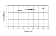
- 2 is a graph showing the relationship between the pulse time width of pulsed light output from an optical fiber amplifier and the average output of the optical fiber amplifier.
- 2 is a graph showing the relationship between the spectral width of pulsed light output from an optical fiber amplifier and the average output of the optical fiber amplifier.
- 2 is a graph showing the relationship between the amount of chirp (GDD) of pulsed light output from an optical fiber amplifier and the average output of the optical fiber amplifier.
- FIG. 2 is a schematic configuration diagram of a light source unit.
- FIG. 3 is a plan view of the compressor. It is a side view of a compressor.
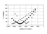
- FIG. 3 is a graph showing compression characteristics of pulse time width of pulsed light output from an optical fiber amplifier.
- 2 is a flowchart showing the flow of a scanning method using pulsed light.
- FIG. 7 is a schematic configuration diagram of a light source unit according to a modification. It is a top view of the compressor concerning a modification.
- FIG. 7 is a schematic configuration diagram of an optical device according to a modification. It is a graph which shows the compression characteristic of the pulse time width of pulsed light in the optical device based on a modification.
- FIG. 2 is a schematic configuration diagram showing a microscope device including an optical device according to a second embodiment.
- the optical processing apparatus 1 includes a stage 5, an optical device 10, and an observation unit 60.
- the optical processing device 1 controls the optical device 10, the stage 5, etc. using a control device (not shown) based on the processing data created according to the desired shape, thereby processing the workpiece W, which is the object to be processed. It is possible to process it into a desired shape.
- a workpiece W is placed on the upper surface of the stage 5.
- the material of the work W may be, for example, metal, resin, or glass.
- the stage 5 may be configured to be able to displace the work W placed on the upper surface of the stage 5 at least in a direction perpendicular to the optical axis of the optical processing device 1.
- the observation unit 60 includes an illumination light source 61, a half mirror 62, an imaging lens 63, and an imaging section 64. Furthermore, the observation unit 60 includes the dichroic mirror 15 of the optical device 10 and the objective lens 17.
- the illumination light source 61 is configured using an LED (Light Emitting Diode) or the like.
- the illumination light source 61 emits illumination light in the wavelength band of visible light.
- the half mirror 62 reflects a part of the illumination light emitted from the illumination light source 61 toward the dichroic mirror 15 .
- the half mirror 62 transmits the light from the workpiece W reflected by the dichroic mirror 15 toward the imaging lens 63 .
- the ratio of transmittance and reflectance of the half mirror 62 is set to, for example, 1:1.
- the imaging lens 63 forms an image of the light from the workpiece W that has passed through the half mirror 62.
- the imaging unit 64 is configured using an imaging element such as a CCD (Charge Coupled Device) or a CMOS (Complementary Metal Oxide Semiconductor).
- the imaging unit 64 captures an image of the workpiece W formed by the imaging lens 63.
- the image of the workpiece W captured by the imaging unit 64 is displayed on a display device (not shown). It is possible to observe the work W through the image displayed on the display device. Note that the control amount of the optical device 10 and the stage 5 by the control device (not shown) may be corrected based on the image data of the workpiece W captured by the image capturing section 64.
- the optical device 10 focuses pulsed light PL on the workpiece W.
- the pulse time width of the pulsed light PL is, for example, a time width on the order of femtoseconds (fs).
- fs femtoseconds
- pulsed light PL is also referred to as ultrashort pulsed light, it will be simply referred to as "pulsed light” in the following description.
- a technique called time focusing is used.
- time focus a technique called time focus may be simply referred to as "time focus.”
- the optical axis direction of the optical processing device 1 (or microscope device 101) including the optical device 10 may be referred to as the z direction, and the directions perpendicular to the optical axis may be referred to as the x direction and the y direction.
- the directions indicated by the arrows in FIGS. 2, 7, 8, and 11 are referred to as the x direction, y direction, and z direction, respectively.
- pulsed light is focused on an object surface (for example, the surface to be processed of the workpiece W).
- the condensing radius of the pulsed light is w
- the wave number of the pulsed light is k
- the wavelength of the pulsed light is ⁇ .
- the region where the light intensity of the pulsed light is high i.e., the confocal length
- the confocal length is limited to about 6 ⁇ m in the z direction. This is an area where If the convergence radius w of the pulsed light is increased to approximately 50 ⁇ m, the confocal length will be approximately 16 mm, and the resolution of the optical processing device in the optical axis direction (z direction) will be reduced.
- FIG. 2 shows an example of an optical system using temporal focus.
- a diffraction grating 510 disperses pulsed light PL emitted from a light source unit (not shown) by a diffraction phenomenon.
- the pulsed light PL dispersed in the diffraction grating 510 enters the collimator lens 520.
- the pulsed light PL transmitted through the collimator lens 520 becomes parallel and enters the objective lens 530.
- the pulsed light PL transmitted through the objective lens 530 is focused on an object plane OB located at the focal point of the objective lens 530.
- the object surface OB is the surface to be processed unless otherwise specified.
- the diffraction grating 510 and the object plane OB are conjugate with each other.
- the pulse time width of the pulsed light PL increases.
- the pulse time width of the pulsed light PL decreases, and the original The pulse time width of is reproduced. This phenomenon is called time focus.
- the pulse time width of the pulsed light PL becomes relatively large, so the peak power of the pulsed light PL decreases, and the processing efficiency by the pulsed light PL decreases. As a result, it becomes possible to improve the resolution of the optical processing device in the optical axis direction (z direction).
- the pulse time width of the pulsed light PL in the vicinity of the object plane OB is approximately expressed by the following equation (1).
- Transform Limited Pulse Transform Limited Pulse
- GDD Group Delay Dispersion
- f indicates the focal length of the objective lens 530.
- k 0 indicates the wave number at the center frequency in the spectrum of the pulsed light PL dispersed in the diffraction grating 510.
- the frequency ⁇ is offset so that the center frequency in the spectrum of the pulsed light PL is zero (0).
- ⁇ is a coefficient determined by the dispersion (or linear density, angle of incidence) of the diffraction grating 510, the focal length fc of the collimator lens 520, and the like.
- ⁇ is the maximum frequency in the spectrum of the pulsed light PL.
- the width of the pulsed light PL in the x direction at the incident position with respect to the objective lens 530 (that is, the width in the dispersion direction of the pulsed light PL dispersed in the diffraction grating 510) is approximately 2 ⁇ .
- the diameter s of a monochromatic wave in the spectrum of the pulsed light PL is s ⁇ .
- the resolution of the optical processing device in the z direction will be on the order of ⁇ m due to the effect of time focusing.
- the resolution of the optical processing device in the optical axis direction increases, making it possible to perform fine processing such as removal processing on the workpiece. It becomes possible to do so.
- the material of the workpiece is transparent resin or glass, the effect of time focusing makes it possible to perform fine processing on the inside of the workpiece.
- the position in the z direction where the time focus occurs can be changed by chirping the pulsed light PL (changing the frequency with time).
- the amount of chirp is expressed using GDD (fs 2 or ps 2 ) at the lowest order.
- the relationship between the amount ⁇ of chirp and the change ⁇ z in the position in the z direction at which time focus occurs is approximately expressed by the following equation (3).
- ⁇ GDD/2.
- z R ⁇ 10 ⁇ m
- ⁇ ⁇ 0.033 rad/fs corresponding to pulsed light of ⁇ 70 fs
- the pulsed light of the Fourier limit pulse there are methods such as passing it through a glass material such as quartz, and using a prism pair or a diffraction grating pair (grating pair).
- a prism pair the GDD of the pulsed light can be changed by changing the spacing between the prisms or the degree of insertion of the prisms into the optical path.
- the GDD of pulsed light can be changed by changing the spacing between the diffraction gratings.
- temporal focusing is created by changing the GDD by about 11000 fs 2 by adjusting the prism pair. It has been experimentally shown that it is possible to change the position by 140 ⁇ m. In this method, since the position of the prism is changed mechanically, it takes time to change the position where the temporal focus occurs. In this embodiment, a light source unit using an optical fiber amplifier and an optical system using time focus are combined to rapidly change the position where time focus occurs.
- An optical fiber amplifier is composed of an optical fiber having a length of about 1 m to several tens of meters.
- the core diameter of the optical fiber is approximately several ⁇ m to several tens of ⁇ m. Since such a long optical fiber with a small core diameter is used, both dispersion and nonlinearity in the optical fiber amplifier are large.
- the pulse time width and spectrum width of the pulsed light output from the optical fiber amplifier change depending on the amplification factor of the optical fiber amplifier.
- the chirp (GDD) of pulsed light is approximately proportional to "pulse time width/spectral width (ps/nm)".
- Figure 3 shows the relationship between the pulse time width of the pulse light output from the optical fiber amplifier and the average output of the optical fiber amplifier.
- Figure 4 shows the relationship between the spectral width of the pulse light output from the optical fiber amplifier and the average output of the optical fiber amplifier.
- pulse light with a period of 350 fs and a wavelength of 1.56 ⁇ m is used as the input to the optical fiber amplifier.
- the optical fiber amplifier used is an Erbium Doped Fiber Amplifier (EDFA) with a length of up to 16 m, a mode field diameter (MFD) of up to 5 ⁇ m, and normal dispersion.
- the average output of the optical fiber amplifier is proportional to the pulse energy (energy per pulse) of the pulse light.
- Figures 3 and 4 show that the rate of increase in the spectral width when the pulse energy is increased is greater than the rate of increase in the average output of the optical fiber amplifier, i.e., the rate of increase in the pulse time width when the pulse energy is increased.
- FIG. 5 shows the relationship between the amount of chirp (GDD) of the pulsed light output from the optical fiber amplifier and the average output of the optical fiber amplifier, which was determined from FIGS. 3 and 4.
- Figure 5 shows that the amount of chirp (GDD) of the pulsed light output from the optical fiber amplifier varies from 0.17 to 0.2 ps 2 (170,000 to 200,000 fs 2 ) depending on the average output of the optical fiber amplifier, that is, changes in pulse energy. ).
- the optical device 10 includes a light source unit 20, a first mirror 11, a diffraction grating 12, a collimator lens 13, a second mirror 14, a dichroic mirror 15, It has an objective lens 17.
- the light source unit 20 emits pulsed light PL in a wavelength band of 1 ⁇ m, for example.
- the first mirror 11 reflects the pulsed light PL emitted from the light source unit 20 toward the diffraction grating 12 .
- the diffraction grating 12 disperses the pulsed light PL reflected by the first mirror 11 by a diffraction phenomenon.
- the collimator lens 13 makes the pulsed light PL dispersed in the diffraction grating 12 parallel.
- the second mirror 14 reflects the pulsed light PL that has passed through the collimator lens 13 toward the dichroic mirror 15.
- a galvano mirror (not shown) may be provided that reflects the pulsed light PL transmitted through the collimator lens 13 toward the dichroic mirror 15.
- the galvanometer mirror can change the traveling direction of the pulsed light PL by changing the direction of the reflecting surface. By changing the traveling direction of the pulsed light PL using a galvanometer mirror, it is possible to scan the workpiece W on a plane (workpiece surface) perpendicular to the optical axis of the objective lens 17. It is desirable that the galvanometer mirror be provided at the position of the pupil of the objective lens 17 or at a position conjugate with the pupil.
- the dichroic mirror 15 transmits the pulsed light PL that has entered the dichroic mirror 15 toward the objective lens 17 . Further, the dichroic mirror 15 reflects illumination light from the observation unit 60 (half mirror 62) that has entered the dichroic mirror 15 toward the objective lens 17. The dichroic mirror 15 reflects the light (visible light) from the workpiece W that has entered the dichroic mirror 15 via the objective lens 17 toward the observation unit 60 (half mirror 62).
- the objective lens 17 focuses the pulsed light PL transmitted through the dichroic mirror 15 onto the workpiece W. Note that the diffraction grating 12 and the workpiece W (workpiece surface) are conjugate with each other. Further, the objective lens 17 irradiates the workpiece W with the illumination light reflected by the dichroic mirror 15. Light from the workpiece W irradiated with illumination light enters the objective lens 17 . Light (visible light) from the workpiece W that has entered the objective lens 17 is transmitted through the objective lens 17 and reflected by the dichroic mirror 15.
- the light source unit 20 includes an oscillator 22, a first optical isolator 23, a second optical isolator 24, a first optical fiber amplifier 25, a second optical fiber amplifier 26, and a collimator lens 29. , and a compressor 31.
- the oscillator 22 is configured using a mode-locked fiber laser.
- the oscillator 22 generates pulsed light that is a Fourier limit pulse with a pulse time width of about 100 fs to 1 ps.
- the first optical isolator 23 is provided between the oscillator 22 and the first optical fiber amplifier 25.
- the second optical isolator 24 is provided between the first optical fiber amplifier 25 and the second optical fiber amplifier 26.
- the first optical isolator 23 and the second optical isolator 24 transmit only pulsed light traveling in the forward direction and block light traveling in the reverse direction.
- the first optical fiber amplifier 25 is configured using a normal dispersion erbium-doped optical fiber amplifier (EDFA).
- the first optical fiber amplifier 25 may be configured using a normal dispersion Ytterbium Doped Fiber Amplifier (YDFA).
- the first optical fiber amplifier 25 is provided with a first pump LD (laser diode) 27 .
- the first pump LD 27 makes excitation light (also referred to as pump light) enter the first optical fiber amplifier 25 .
- the first optical fiber amplifier 25 amplifies the pulsed light generated from the oscillator 22 using the excitation light incident from the first pump LD 27. By changing the excitation current of the first pump LD 27, it is possible to change the amplification factor (ie, output) of the first optical fiber amplifier 25.
- the first optical fiber amplifier 25 is an optical fiber amplifier that is longer than the second optical fiber amplifier 26 and has a smaller core diameter. As a result, the chirp characteristics (GDD) of the pulsed light are determined by the first optical fiber amplifier 25, which has relatively large dispersion and nonlinearity.
- the second optical fiber amplifier 26 is configured using an erbium-doped optical fiber amplifier (EDFA).
- the second optical fiber amplifier 26 may be configured using a ytterbium-doped optical fiber amplifier (YDFA).
- the second optical fiber amplifier 26 is provided with a second pump LD (laser diode) 28.
- the second pump LD 28 causes excitation light (also referred to as pump light) to enter the second optical fiber amplifier 26 .
- the second optical fiber amplifier 26 amplifies the pulsed light output from the first optical fiber amplifier 25 using the excitation light incident from the second pump LD 28.
- By changing the excitation current of the second pump LD 28 it is possible to change the amplification factor (ie, output) of the second optical fiber amplifier 26.
- the second optical fiber amplifier 26 is an optical fiber amplifier that is shorter than the first optical fiber amplifier 25 and has a larger core diameter. As a result, the output (pulse energy of the pulsed light) is determined by the second optical fiber amplifier 26, which has relatively small dispersion and nonlinearity.
- the amplifiers By using the first optical fiber amplifier 25, which has relatively large dispersion and nonlinearity, and the second optical fiber amplifier 26, which has relatively small dispersion and nonlinearity, the amplifiers (first optical fiber amplifier 25 and It is possible to reduce fluctuations in the pulse energy of the pulsed light while changing the amount of chirp (GDD) of the pulsed light output from the second optical fiber amplifier 26).
- GDD amount of chirp
- the second optical fiber amplifier 26 may be omitted. In that case, in the following description, the output of the second optical fiber amplifier 26 may be read as the output of the first optical fiber amplifier 25.
- the collimator lens 29 collimates the pulsed light output from the second optical fiber amplifier 26.
- the compressor 31 compresses the pulse time width of the pulsed light outputted from the second optical fiber amplifier 26 and transmitted through the collimator lens 29, and emits the pulsed light PL, which is a Fourier limit pulse.
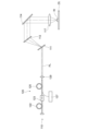
- the compressor 31 includes an output mirror 32, a diffraction grating pair of a first diffraction grating 33 and a second diffraction grating 34, and a roof mirror 35.
- the pulsed light that has passed through the collimator lens 29 passes through a position away from the output mirror 32 in the -y direction perpendicular to the optical axis.
- the pulsed light that has passed through the output mirror 32 is spatially dispersed by the first diffraction grating 33 and the second diffraction grating 34.
- the pulsed light dispersed by the first diffraction grating 33 and the second diffraction grating 34 is reflected by the roof mirror 35 and returns to the second diffraction grating 34 and the first diffraction grating 33 in this order.
- the pulsed light that has returned to the second diffraction grating 34 and first diffraction grating 33 is offset in the +y direction by the roof mirror 35, so it is reflected by the output mirror 32 and emitted to the outside (first mirror 11).
- Ru Although such a compressor 31 has negative dispersion (GDD ⁇ 0), the dispersion of the compressor 31 can be changed by changing the interval between the first diffraction grating 33 and the second diffraction grating 34. be able to.
- FIG. 9 shows the compression characteristics of the pulse time width of the pulsed light output from the two-stage amplifier (the first optical fiber amplifier 25 and the second optical fiber amplifier 26) shown in FIG.
- the axis indicates the pulse time width (fs) of pulsed light.
- the mark ⁇ in the graph shown in FIG. 9 indicates the compression characteristic when the excitation current of the first pump LD 27 in the first optical fiber amplifier 25 is 600 mA.
- the black mark in the graph shown in FIG. 9 indicates the compression characteristic when the excitation current of the first pump LD 27 in the first optical fiber amplifier 25 is 1000 mA.
- the excitation current of the first pump LD27 in the first optical fiber amplifier 25 is 600 mA or 1000 mA
- the excitation current of the second pump LD28 in the second optical fiber amplifier 26 is constant.
- the amount of dispersion of the compressor 31 to obtain the minimum pulse time width is -0.163 ps 2 , that is, the amount of chirp of the pulsed light (GDD ) was + 0.163ps2 .
- the excitation current of the first pump LD 27 in the first optical fiber amplifier 25 is 1000 mA
- the amount of dispersion of the compressor 31 to obtain the minimum pulse time width is -0.148 ps 2 , that is, the amount of chirp of the pulsed light (GDD ) was + 0.148ps2 .
- the two-stage amplifier the first optical fiber amplifier 25 and the second optical fiber amplifier 26
- the excitation current of the first pump LD 27 in the first optical fiber amplifier 25 was 600 mA
- the output of the second optical fiber amplifier 26 was 477 mW.
- the output of the second optical fiber amplifier 26 was 537 mW.
- the excitation current of the second pump LD28 in the second optical fiber amplifier 26 is kept constant, so the output of the second optical fiber amplifier 26 varies slightly, but the excitation current of the second pump LD28 is adjusted. By doing so, it is also possible to maintain the output of the second optical fiber amplifier 26 within a certain range.
- the excitation current of the first pump LD 27 in the first optical fiber amplifier 25 is 600 mA or 1000 mA
- the minimum pulse time width of the pulsed light is almost the same ( ⁇ 115 fs).
- the first optical fiber amplifier 25 and the second optical fiber amplifier 26 are erbium-doped optical fiber amplifiers (EDFA) or ytterbium-doped optical fiber amplifiers (YDFA)
- EDFA erbium-doped optical fiber amplifiers
- YDFA ytterbium-doped optical fiber amplifiers
- the gain response to the modulation of the excitation light (pump light) of the second pump LD 28 ie, the gain response to the modulation of the excitation current
- GDD amount of chirp
- this method it is possible to change the amount of chirp (GDD) of pulsed light easily and quickly compared to mechanical methods such as changing the position of a prism.
- GDD amount of chirp
- FIG. 10 is a flowchart showing the flow of a scanning method using pulsed light.
- pulsed light is generated by the oscillator 22 of the light source unit 20 (step ST1).
- the oscillator 22 generates pulsed light that is a Fourier limit pulse.
- the pulsed light is amplified by the first optical fiber amplifier 25 and the second optical fiber amplifier 26 (step ST2).
- the pulsed light generated from the oscillator 22 passes through the first optical isolator 23 and enters the first optical fiber amplifier 25.
- the first optical fiber amplifier 25 amplifies the pulsed light generated from the oscillator 22.
- the pulsed light output from the first optical fiber amplifier 25 passes through the second optical isolator 24 and enters the second optical fiber amplifier 26 .
- the second optical fiber amplifier 26 amplifies the pulsed light output from the first optical fiber amplifier 25.
- the pulsed light output from the second optical fiber amplifier 26 passes through the collimator lens 29, becomes parallel, and enters the compressor 31.
- the compressor 31 compresses the pulse time width of the pulsed light that has passed through the collimator lens 29, and emits the pulsed light PL, which is a Fourier limit pulse.
- the pulsed light is dispersed by the diffraction grating 12 (step ST3).
- Pulsed light PL emitted from the compressor 31 of the light source unit 20 is reflected by the first mirror 11 and enters the diffraction grating 12 .
- the diffraction grating 12 disperses the pulsed light PL reflected by the first mirror 11 by a diffraction phenomenon.
- the pulsed light PL dispersed in the diffraction grating 12 passes through the collimator lens 13, becomes parallel, and enters the second mirror 14. At this time, the diffraction grating 12 and the collimator lens 13 generate a spatial chirp in the pulsed light PL, which is necessary for time focusing.
- the pulsed light is focused by the objective lens 17 (step ST4).
- the pulsed light PL reflected by the second mirror 14 passes through the dichroic mirror 15 and enters the objective lens 17 .
- the objective lens 17 focuses the pulsed light PL transmitted through the dichroic mirror 15 onto the workpiece W.
- the pulse time width of the pulsed light PL is reduced due to the effect of time focusing, and the original pulse time width when incident on the diffraction grating 12 on the processed surface of the workpiece W is reproduced.
- the resolution in the optical axis direction (z direction) of the optical processing device 1 can be increased due to the effect of time focusing, and the It becomes possible to perform fine processing such as removal processing.
- the material of the workpiece W is transparent resin or glass, it becomes possible to perform fine processing on the inside of the workpiece W due to the effect of time focusing. Note that, as described above, the pulse time width of the pulsed light PL focused by the objective lens 17 becomes the pulse time width of the pulsed light PL when it enters the diffraction grating 12 due to time focusing.
- scanning is performed by changing the position where the temporal focus occurs in the optical axis direction of the objective lens 17 (step ST5).
- the amplification factors of the first optical fiber amplifier 25 and the second optical fiber amplifier 26 are changed by modulating the excitation currents of the first pump LD27 and the second pump LD28.
- the amount of chirp (GDD) of the pulsed light PL is changed, and the position where time focus occurs is changed in the optical axis direction of the objective lens 17, thereby performing scanning in the optical axis direction (z direction).
- the above-mentioned step of generating the pulsed light (ST1), step of amplifying the pulsed light (ST2), and step of amplifying the pulsed light are performed.
- the step of dispersing (ST3), the step of focusing pulsed light (ST4), and the step of scanning (ST5) are each performed in parallel.
- the optical device 10 of the optical processing apparatus 1 includes a first optical fiber amplifier 25 and a second optical fiber amplifier 26 that amplify pulsed light, a diffraction grating 12 that disperses pulsed light, and a diffraction grating. 12, and an objective lens 17 for condensing the dispersed pulsed light, and it is possible to change the amplification factors of the first optical fiber amplifier 25 and the second optical fiber amplifier 26 independently.
- the pulse time width of the pulsed light focused by the objective lens 17 becomes the pulse time width of the pulsed light when it enters the diffraction grating 12 due to time focusing.
- the excitation current of the first pump LD 27 by modulating the excitation current of the first pump LD 27 at high speed, it is possible to change the amplification factor of the first optical fiber amplifier 25 at high speed, so that the amount of chirp (GDD) of the pulsed light can be changed at high speed, and the position where time focus occurs (position in the z direction) can be changed at high speed to perform scanning in the optical axis direction at high speed.
- GDD amount of chirp
- the resolution in the optical axis direction (z direction) of the optical processing device 1 increases, so by changing the position where time focus occurs (position in the z direction) at high speed, it is possible to This makes it possible to perform fine processing such as removal processing at high speed.
- the amplification factor of the second optical fiber amplifier 26 can be adjusted, and the amount of chirp (GDD) of the pulsed light can be changed while changing the output of the pulsed light. It is possible to keep it within a certain range.
- a light amount regulator such as an acousto-optic device (AOM) may be installed on the input side or output side of the second optical fiber amplifier 26 to control the pulse energy of the pulsed light.
- AOM acousto-optic device
- a compressor 31 may be provided to compress the pulse time width of the pulsed light output from the second optical fiber amplifier 26. Thereby, pulsed light that is a Fourier limit pulse can be obtained.
- the oscillator 22 is provided in the first embodiment described above, the present invention is not limited to this.
- the oscillator 22 may not be provided, and the first optical fiber amplifier 25 may amplify pulsed light from a pulsed light generator provided outside the optical processing apparatus 1.
- the step (ST1) of generating the pulsed light described above can be omitted.
- the diffraction grating 12 that disperses the pulsed light by a diffraction phenomenon is provided, but the present invention is not limited to this.
- a prism or the like may be provided instead of the diffraction grating 12 as a dispersion element that disperses the pulsed light. Note that dispersing the pulsed light using a dispersion element means spatially separating the optical path of the pulsed light according to the wavelength of the pulsed light.
- the amplification factors of the first optical fiber amplifier 25 and the second optical fiber amplifier 26 are changed by modulating the excitation currents of the first pump LD 27 and the second pump LD 28. It is not limited to. For example, by controlling the amount of input pulsed light using an acousto-optic device (AOM) or the like provided on the input side of the first optical fiber amplifier 25, the amplification factor of the first optical fiber amplifier 25 can be effectively changed, and the pulse The amount of chirp (GDD) of the light may be changed.
- AOM acousto-optic device
- the amplification factor of the second optical fiber amplifier 26 can be effectively changed by controlling the amount of pulsed light using an acousto-optic device (AOM) or the like provided on the input side or the output side of the second optical fiber amplifier 26.
- AOM acousto-optic device
- the output of the second optical fiber amplifier 26 may be kept within a certain range.
- the light source unit 20 has a two-stage amplifier (the first optical fiber amplifier 25 and the second optical fiber amplifier 26), but is not limited to this. You may have only one.
- the light source unit 70 may include an oscillator 22, an optical isolator 73, an optical fiber amplifier 75, a collimator lens 29, and a compressor 31.
- the optical isolator 73 is configured similarly to the first optical isolator 23 according to the first embodiment.
- the optical fiber amplifier 75 is configured similarly to the first optical fiber amplifier 25 according to the first embodiment.
- the collimator lens 29 collimates the pulsed light output from the optical fiber amplifier 75.
- the optical fiber amplifier 75 is provided with a pump LD 77.
- the pump LD77 is configured similarly to the first pump LD27 according to the first embodiment, and by changing the excitation current of the pump LD77, it is possible to change the amplification factor (ie, output) of the optical fiber amplifier 75.
- the oscillator 22 may not be provided, and the optical fiber amplifier 75 may amplify pulsed light from a pulsed light generator provided outside the optical processing apparatus.
- the compressor 31 is configured using a diffraction grating pair (grating pair), but is not limited to this, and may be configured using a prism pair.
- the compressor 131 may include an output mirror 32, a prism pair of a first prism 133 and a second prism 134, and a roof mirror 35.
- the pulsed light that has passed through the collimator lens 29 passes through a position away from the output mirror 32 in the -y direction perpendicular to the optical axis.
- the pulsed light that has passed through the output mirror 32 is spatially dispersed by the first prism 133 and the second prism 134.
- the pulsed light dispersed by the first prism 133 and the second prism 134 is reflected by the roof mirror 35 and returns to the second prism 134 and the first prism 133 in this order. Since the pulsed light that has returned to the second prism 134 and first prism 133 in this order is offset in the +y direction by the roof mirror 35, it is reflected by the output mirror 32 and emitted to the outside (first mirror 11). Although such a compressor 131 has a negative dispersion (GDD ⁇ 0), the dispersion of the compressor 131 can be changed by changing the distance between the first prism 133 and the second prism 134. can.
- an optical device 110 includes a light source unit 120, a diffraction grating pair of a first diffraction grating 111 and a second diffraction grating 112, a mirror 114, and an objective lens 117.
- the light source unit 120 includes an oscillator 122, an optical isolator 123, an optical fiber amplifier 125, and a collimator lens 129.
- the oscillator 122 is configured using a mode-locked fiber laser.
- the oscillator 122 generates pulsed light that is a Fourier limit pulse with a pulse time width of about 100 fs to 1 ps.
- Optical isolator 123 is provided between oscillator 122 and optical fiber amplifier 125. The optical isolator 123 transmits only pulsed light traveling in the forward direction and blocks light traveling in the reverse direction.
- the optical fiber amplifier 125 is configured using a normal dispersion erbium-doped optical fiber amplifier (EDFA).
- the optical fiber amplifier 125 may be configured using a normal dispersion ytterbium-doped optical fiber amplifier (YDFA).
- the optical fiber amplifier 125 is provided with a pump LD (laser diode) 127.
- the pump LD 127 makes excitation light (pump light) enter the optical fiber amplifier 125.
- the optical fiber amplifier 125 amplifies the pulsed light generated from the oscillator 122 using the excitation light incident from the pump LD 127. By changing the excitation current of the pump LD 127, it is possible to change the amplification factor (ie, output) of the optical fiber amplifier 125.
- the collimator lens 129 collimates the pulsed light output from the optical fiber amplifier 125.
- the optical fiber amplifier may be the two-stage amplifier (the first optical fiber amplifier 25 and the second optical fiber amplifier 26) according to the first embodiment described above.
- the oscillator 122 may not be provided, and an optical fiber amplifier may amplify pulsed light from a pulsed light generator provided outside the optical processing apparatus.
- the light source unit 120 emits pulsed light PL having a positive chirp via the optical fiber amplifier 125. If the GDD of the pulsed light PL emitted from the light source unit 120 is Dp, then Dp>0.
- a spatial chirp occurs in the pulsed light PL that has passed through the diffraction grating pair of the first diffraction grating 111 and the second diffraction grating 112.
- the pulsed light double passes through the pair of diffraction gratings, so no spatial chirp occurs and the pulse time width of the Fourier-limited pulse is obtained.
- the pulsed light PL that has passed through the diffraction grating pair of the first diffraction grating 111 and the second diffraction grating 112 is reflected by the mirror 114 and focused onto the workpiece W by the objective lens 117.
- the dichroic mirror (not shown) according to the first embodiment described above may be provided between the mirror 114 and the objective lens 117.
- the pulse time width of the pulsed light PL immediately after passing through the objective lens 117 is maximum, and as it approaches the work W (focal plane of the objective lens 117), the pulse time width of the pulsed light PL becomes smaller, and the workpiece W to be processed is The pulse time width of the pulsed light PL becomes minimum at the plane (focal plane of the objective lens 117).
- the diffraction grating pair of the first diffraction grating 111 and the second diffraction grating 112 removes the GDD of the pulsed light PL emitted from the light source unit 120 and at the same time removes the GDD of the pulsed light PL emitted from the light source unit 120. It can also be said that a spatial chirp necessary for time focusing is given to the pulsed light PL. As a result, as in the first embodiment described above, by rapidly modulating the excitation current of the pump LD 127, it is possible to rapidly change the amplification factor of the fiber amplifier 125, thereby reducing the amount of chirp in the pulsed light.
- GDD can be changed at high speed, and the position where time focus occurs (position in the z direction) can be changed at high speed.
- the effect of time focus increases the resolution of the optical processing device in the optical axis direction (z direction), so by rapidly changing the position where time focus occurs (position in the z direction), It becomes possible to perform fine processing such as removal processing with high resolution and at high speed.
- FIG. 14 shows the compression characteristics of the pulse time width of the pulsed light output from the optical fiber amplifier 125 of the optical device 110 according to the modification.
- the horizontal axis of the graph shown in FIG. 14 is the dispersion amount (fs 2 ) of the diffraction grating pair (first diffraction grating 111 and second diffraction grating 112) placed after the optical fiber amplifier 125 as a compressor, and the vertical axis is the dispersion amount (fs 2 ) as a compressor.
- the pulse time width (fs) of pulsed light is shown.
- the compressor had a double-pass configuration.
- the black mark in the graph shown in FIG. 14 indicates the compression characteristic when the excitation current of the pump LD 127 in the optical fiber amplifier 125 is 2.8 A.
- the mark ⁇ in the graph shown in FIG. 14 indicates the compression characteristic when the excitation current of the pump LD 127 in the optical fiber amplifier 125 is 5.0 A.
- the output of the optical fiber amplifier 125 was 122 mW.
- the output of the optical fiber amplifier 125 was 918 mW.
- the output of the optical fiber amplifier 125 was 1970 mW.
- the amount of chirp (GDD) of the pulsed light output from the optical fiber amplifier 125 can be changed by about 48000 fs 2 is possible.
- the minimum pulse time width of the pulsed light is almost the same ( ⁇ 90 fs).
- GDD amount of chirp
- a microscope device 201 includes a stage 205, an optical device 210, and a detection unit 260.
- the microscope device 201 is also referred to as a two-photon excitation fluorescence microscope or a multiphoton excitation fluorescence microscope.
- a sample SA is placed on the upper surface of the stage 205. Sample SA may be, for example, a cell.
- the detection unit 260 has a condensing lens 261 and a detection section 262. Further, the detection unit 260 includes a dichroic mirror 215 of the optical device 210, galvano mirrors 216, 216, and an objective lens 217.
- the condensing lens 261 condenses the fluorescence from the sample SA reflected by the dichroic mirror 215.
- the detection unit 262 is configured using a photomultiplier tube (PMT), a photodiode (PD), or the like.
- the detection unit 262 detects the fluorescence from the sample SA focused by the condenser lens 261 and outputs a detection signal. Based on the detection signal detected by the detection unit 262, an image processing unit (not shown) performs image processing, and an image of the sample SA obtained by the image processing in the image processing unit is displayed on a display device (not shown). Ru.
- the optical device 210 focuses pulsed light, which is excitation light, on the sample SA.
- the pulse time width of the pulsed light is, for example, a time width on the order of femtoseconds (fs).
- the optical device 210 includes a light source unit 20, a first mirror 11, a diffraction grating 12, a collimator lens 13, a second mirror 14, a dichroic mirror 215, and galvano mirrors 216, 216. , and an objective lens 217.
- the light source unit 20, the first mirror 11, the diffraction grating 12, the collimator lens 13, and the second mirror 14 are the light source unit 20, the first mirror 11, the diffraction grating 12, the collimator lens 13, and the second mirror according to the first embodiment. It has the same configuration as the mirror 14, is given the same reference numeral as in the first embodiment, and detailed description thereof will be omitted.
- the dichroic mirror 215 transmits the pulsed light PL that has entered the dichroic mirror 215 toward the galvano mirrors 216 and 216. Further, the dichroic mirror 215 reflects the fluorescence from the sample SA that has entered the dichroic mirror 215 via the objective lens 217 and the galvano mirrors 216, 216 toward the detection unit 260 (condensing lens 261).
- the galvano mirrors 216 and 216 reflect the pulsed light PL that has passed through the dichroic mirror 215 toward the objective lens 217. Further, the galvano mirrors 216 and 216 reflect the fluorescence from the sample SA that has passed through the objective lens 217 toward the dichroic mirror 215.
- the galvano mirrors 216, 216 can change the traveling direction of the pulsed light PL by changing the direction of the reflecting surface. By changing the traveling direction of the pulsed light PL using the galvanometer mirrors 216, 216, it is possible to scan the sample SA in a plane (observation plane) perpendicular to the optical axis of the objective lens 217. It is desirable that the galvano mirrors 216, 216 be provided at the position of the pupil of the objective lens 217 or at a position conjugate with the pupil.
- the objective lens 217 focuses the pulsed light PL reflected by the galvano mirrors 216, 216 onto the sample SA. Note that the diffraction grating 12, sample SA (observation surface), and detection unit 262 are conjugate with each other.
- step ST1 pulsed light is generated in the same manner as in the first embodiment (step ST1).
- step ST2 the pulsed light is amplified in the same manner as in the first embodiment (step ST2).
- the pulsed light is dispersed by the diffraction grating 12 (step ST3).
- the light source unit 20 emits, for example, pulsed light PL in a wavelength band of 1 ⁇ m as excitation light.
- Pulsed light PL emitted from the light source unit 20 is reflected by the first mirror 11 and enters the diffraction grating 12 .
- the diffraction grating 12 disperses the pulsed light PL reflected by the first mirror 11 by a diffraction phenomenon.
- the pulsed light PL dispersed in the diffraction grating 12 passes through the collimator lens 13, becomes parallel, and enters the second mirror 14.
- the diffraction grating 12 and the collimator lens 13 generate a spatial chirp in the pulsed light PL, which is necessary for time focusing.
- the pulsed light is focused by the objective lens 217 (step ST4).
- the pulsed light PL reflected by the second mirror 14 passes through the dichroic mirror 215 and is reflected by the galvano mirrors 216, 216.
- the pulsed light PL reflected by the galvanometer mirrors 216 and 216 enters the objective lens 217.
- the objective lens 217 focuses the pulsed light PL reflected by the galvano mirrors 216, 216 onto the sample SA. Note that the pulse time width of the pulsed light PL focused by the objective lens 217 becomes the pulse time width of the pulsed light PL when it enters the diffraction grating 12 due to time focusing.
- scanning is performed by changing the position where the temporal focus occurs in the optical axis direction of the objective lens 217 (step ST5).
- the amplification factors of the first optical fiber amplifier 25 and the second optical fiber amplifier 26 are changed by modulating the excitation currents of the first pump LD27 and the second pump LD28.
- the amount of chirp (GDD) of the pulsed light PL is changed, and the position where time focus occurs is changed in the optical axis direction of the objective lens 217, thereby performing scanning in the optical axis direction (z direction).
- the traveling direction of the pulsed light PL using the galvanometer mirrors 216, 216, scanning in a direction (XY direction) perpendicular to the optical axis of the objective lens 217 is performed.
- the step of generating the pulsed light (ST1), the step of amplifying the pulsed light (ST2), and the step of amplifying the pulsed light described above are performed.
- the step of dispersing (ST3), the step of focusing pulsed light (ST4), and the step of scanning (ST5) are each performed in parallel.
- the fluorescent substance contained in the sample SA is two-photon excited, and fluorescence with a shorter wavelength than the excitation light (pulsed light PL) is emitted.
- the pulse time width of the pulsed light PL is reduced due to the effect of time focusing, and the original pulse time width when it enters the diffraction grating 12 on the observation plane of the sample SA (focal plane of the objective lens 217) is reproduced.
- the resolution of the microscope device 201 in the optical axis direction (z direction) is increased, so two-photon excitation occurs only in a minute region near the focal point of the objective lens 217.
- scanning in the optical axis direction can be performed by changing the position where the time focus occurs (position in the z direction), and this can be combined with scanning in the direction perpendicular to the optical axis by the galvanometer mirrors 216, 216.
- This makes it possible to generate a three-dimensional image of the sample SA.
- the fluorescence from the sample SA enters the objective lens 217.
- the fluorescence transmitted through the objective lens 217 is reflected by the galvanometer mirrors 216 and 216 and enters the dichroic mirror 215.
- the fluorescence that has entered the dichroic mirror 215 is reflected by the dichroic mirror 215 and enters the condenser lens 261 .
- the fluorescence transmitted through the condensing lens 261 is condensed onto the detection section 262. Note that the diffraction grating 12, sample SA (observation surface), and detection unit 262 are conjugate with each other.
- the pulsed light PL which is the excitation light
- the fluorescence that passes through the objective lens 217 out of the fluorescence generated by two-photon excitation is leaked. It is possible to reach the detection unit 262 without any problem.
- the optical device 210 of the microscope device 201 includes the first optical fiber amplifier 25 and the second optical fiber amplifier 26 that amplify pulsed light, the diffraction grating 12 that disperses the pulsed light, and the diffraction grating 12 that disperses the pulsed light. It is possible to change the amplification factors of the first optical fiber amplifier 25 and the second optical fiber amplifier 26. Note that the pulse time width of the pulsed light focused by the objective lens 217 becomes the pulse time width of the pulsed light when it enters the diffraction grating 12 due to time focusing.
- the excitation current of the first pump LD 27 by rapidly modulating the excitation current of the first pump LD 27, it is possible to rapidly change the amplification factor of the first optical fiber amplifier 25, so the amount of chirp of the pulsed light can be changed.
- GDD GDD
- the position where time focus occurs position in the z direction
- the resolution in the optical axis direction (z direction) of the microscope device 201 is high even if the condensing radius of the pulsed light is set to about 5 to 10 ⁇ m.
- scanning in the optical axis direction (z direction) can be performed at high speed. Therefore, by combining scanning in a direction perpendicular to the optical axis by the galvanometer mirrors 216, 216, it becomes possible to generate a three-dimensional image of the sample SA at high speed.
- the pulsed light output from the second optical fiber amplifier 26 can be adjusted.
- the output may be within a certain range.
- a light amount regulator such as an acousto-optic device (AOM) may be installed on the input side or output side of the second optical fiber amplifier 26 to control the pulse energy of the pulsed light. This makes it possible to reduce fluctuations in the pulse energy of the pulsed light while changing the amount of chirp (GDD) of the pulsed light.
- GDD amount of chirp
- a compressor 31 may be provided that compresses the pulse time width of the pulsed light output from the second optical fiber amplifier 26. This makes it possible to obtain pulsed light of Fourier limit pulses.
- the first optical fiber amplifier 25 amplifies pulsed light from a pulsed light generator provided outside the microscope device 201 without providing the oscillator 22. You may also do so. In this case, the step (ST1) of generating the pulsed light described above can be omitted.
- a prism or the like may be provided instead of the diffraction grating 12 as a dispersion element that disperses the pulsed light.
- the first light is The amplification factor of the fiber amplifier 25 may be effectively changed to change the amount of chirp (GDD) of the pulsed light. Furthermore, the amplification factor of the second optical fiber amplifier 26 can be effectively changed by controlling the amount of pulsed light using an acousto-optic device (AOM) or the like provided on the input side or the output side of the second optical fiber amplifier 26. However, the output of the second optical fiber amplifier 26 may be kept within a certain range.
- AOM acousto-optic device
- the light source unit 20 is not limited to the two-stage amplifier (the first optical fiber amplifier 25 and the second optical fiber amplifier 26), and may include only one amplifier, as in the first embodiment. You may.
- the compressor 31 is not limited to a diffraction grating pair (grating pair) and may be configured using a prism pair, as in the first embodiment.
- the compressor 31 is provided in the light source unit 20 as in the first embodiment, but the present invention is not limited to this, and the compressor does not need to be provided in the light source unit.
- the optical device of the microscope device 201 may be configured similarly to the optical device 110 according to the modification of the first embodiment.
- a two-photon excitation fluorescence microscope (multiphoton excitation fluorescence microscope) is described as an example of the microscope device 201, but the present invention is not limited to this, and for example, a second harmonic fluorescence microscope is used. It may be a second harmonic generation (SHG) microscope or a third harmonic generation (THG) microscope.
- Optical processing device 10
- Optical device 12 Diffraction grating 13 Collimator lens 17
- Objective lens 20
- Light source unit 22 Oscillator (pulsed light generator) 25
- First optical fiber amplifier 26
- Second optical fiber amplifier 27
- First pump LD 28
- Second pump LD 31
- Compressor 110 Optical device (modified example) 111
- Second diffraction grating 117
- Objective lens 120
- Optical fiber amplifier 127
- Pump LD 201
- Microscope device 210
Landscapes
- Physics & Mathematics (AREA)
- Optics & Photonics (AREA)
- Electromagnetism (AREA)
- Engineering & Computer Science (AREA)
- Plasma & Fusion (AREA)
- General Physics & Mathematics (AREA)
- Nonlinear Science (AREA)
- Chemical & Material Sciences (AREA)
- Analytical Chemistry (AREA)
- Mechanical Engineering (AREA)
- Lasers (AREA)
Priority Applications (5)
| Application Number | Priority Date | Filing Date | Title |
|---|---|---|---|
| KR1020257011241A KR20250060288A (ko) | 2022-09-16 | 2023-09-14 | 광학 장치, 광 가공 장치, 현미경 장치, 및 주사 방법 |
| JP2024547362A JP7786603B2 (ja) | 2022-09-16 | 2023-09-14 | 光学装置、光加工装置、顕微鏡装置、および走査方法 |
| CN202380075577.6A CN120112831A (zh) | 2022-09-16 | 2023-09-14 | 光学装置、光加工装置、显微镜装置、以及扫描方法 |
| EP23865586.4A EP4589357A1 (en) | 2022-09-16 | 2023-09-14 | Optical device, optical machining device, microscope device, and scanning method |
| US19/081,761 US20250279624A1 (en) | 2022-09-16 | 2025-03-17 | Optical device, optical machining device, microscope device, and scanning method |
Applications Claiming Priority (2)
| Application Number | Priority Date | Filing Date | Title |
|---|---|---|---|
| JP2022147880 | 2022-09-16 | ||
| JP2022-147880 | 2022-09-16 |
Related Child Applications (1)
| Application Number | Title | Priority Date | Filing Date |
|---|---|---|---|
| US19/081,761 Continuation US20250279624A1 (en) | 2022-09-16 | 2025-03-17 | Optical device, optical machining device, microscope device, and scanning method |
Publications (1)
| Publication Number | Publication Date |
|---|---|
| WO2024058237A1 true WO2024058237A1 (ja) | 2024-03-21 |
Family
ID=90275246
Family Applications (1)
| Application Number | Title | Priority Date | Filing Date |
|---|---|---|---|
| PCT/JP2023/033478 Ceased WO2024058237A1 (ja) | 2022-09-16 | 2023-09-14 | 光学装置、光加工装置、顕微鏡装置、および走査方法 |
Country Status (6)
| Country | Link |
|---|---|
| US (1) | US20250279624A1 (https=) |
| EP (1) | EP4589357A1 (https=) |
| JP (1) | JP7786603B2 (https=) |
| KR (1) | KR20250060288A (https=) |
| CN (1) | CN120112831A (https=) |
| WO (1) | WO2024058237A1 (https=) |
Citations (3)
| Publication number | Priority date | Publication date | Assignee | Title |
|---|---|---|---|---|
| WO2012135823A1 (en) * | 2011-04-01 | 2012-10-04 | Massachusetts Institute Of Technology | High sensitivity temporal focusing widefield multiphoton endoscope capable of deep imaging |
| JP2017056489A (ja) * | 2015-08-31 | 2017-03-23 | 株式会社リコー | 光加工装置及び光加工物の生産方法 |
| WO2019217846A1 (en) * | 2018-05-10 | 2019-11-14 | Board Of Regents, The University Of Texas System | Line excitation array detection microscopy |
Family Cites Families (1)
| Publication number | Priority date | Publication date | Assignee | Title |
|---|---|---|---|---|
| DE102016211374A1 (de) | 2016-06-24 | 2017-12-28 | Carl Zeiss Microscopy Gmbh | Mikroskopieverfahren unter Nutzung zeitlicher Fokusmodulation und Mikroskop |
-
2023
- 2023-09-14 WO PCT/JP2023/033478 patent/WO2024058237A1/ja not_active Ceased
- 2023-09-14 EP EP23865586.4A patent/EP4589357A1/en active Pending
- 2023-09-14 CN CN202380075577.6A patent/CN120112831A/zh active Pending
- 2023-09-14 KR KR1020257011241A patent/KR20250060288A/ko active Pending
- 2023-09-14 JP JP2024547362A patent/JP7786603B2/ja active Active
-
2025
- 2025-03-17 US US19/081,761 patent/US20250279624A1/en active Pending
Patent Citations (3)
| Publication number | Priority date | Publication date | Assignee | Title |
|---|---|---|---|---|
| WO2012135823A1 (en) * | 2011-04-01 | 2012-10-04 | Massachusetts Institute Of Technology | High sensitivity temporal focusing widefield multiphoton endoscope capable of deep imaging |
| JP2017056489A (ja) * | 2015-08-31 | 2017-03-23 | 株式会社リコー | 光加工装置及び光加工物の生産方法 |
| WO2019217846A1 (en) * | 2018-05-10 | 2019-11-14 | Board Of Regents, The University Of Texas System | Line excitation array detection microscopy |
Non-Patent Citations (1)
| Title |
|---|
| DURST E. ET AL.: "Simultaneous spatial and temporal focus for axial scanning", OPTICS EXPRESS, vol. 14, 2006, pages 12243 |
Also Published As
| Publication number | Publication date |
|---|---|
| EP4589357A1 (en) | 2025-07-23 |
| JP7786603B2 (ja) | 2025-12-16 |
| US20250279624A1 (en) | 2025-09-04 |
| CN120112831A (zh) | 2025-06-06 |
| JPWO2024058237A1 (https=) | 2024-03-21 |
| KR20250060288A (ko) | 2025-05-07 |
Similar Documents
| Publication | Publication Date | Title |
|---|---|---|
| JP5463913B2 (ja) | 広帯域光増幅器、光パルス発生装置及び光学機器 | |
| CN108303806B (zh) | 一种深度成像超分辨显微成像系统 | |
| CN102271859B (zh) | 激光加工装置 | |
| KR102220081B1 (ko) | 레이저의 대역폭 감소를 위한 시스템 및 방법과 레이저를 이용한 검사 시스템 및 방법 | |
| JP5203063B2 (ja) | 多光子励起測定装置 | |
| JP2007538289A (ja) | 共焦点励起平面を有した広視野多光子顕微鏡のための方法およびシステム | |
| JP5076204B2 (ja) | 共焦点走査型顕微鏡法における蛍光の検出のための方法および装置 | |
| JP5309867B2 (ja) | 非線形光学顕微鏡及びその調整方法 | |
| JP2006330685A (ja) | 多光子励起走査型レーザ顕微鏡 | |
| CN212489863U (zh) | 一种快速高效自适应光学补偿的受激拉曼散射成像系统 | |
| JP5139170B2 (ja) | 多光子励起測定装置 | |
| US20160306152A1 (en) | Laser scanning microscope apparatus | |
| Müller et al. | Construction and performance of a custom-built two-photon laser scanning system | |
| JP7786603B2 (ja) | 光学装置、光加工装置、顕微鏡装置、および走査方法 | |
| US20160103310A1 (en) | Two-photon excitated fluorescence microscope | |
| JP2015119012A (ja) | 固体レーザ装置およびそれを用いた非線形計測装置 | |
| KR100790707B1 (ko) | 분산조절 공초점 레이저 현미경 | |
| JP4493302B2 (ja) | 走査型光学顕微鏡 | |
| JP2006275915A (ja) | 多光子励起型観察装置および多光子励起型観察用光源装置 | |
| JP2010160264A (ja) | レーザ顕微鏡 | |
| JP4878751B2 (ja) | 顕微鏡用照明装置および蛍光顕微鏡装置 | |
| Groß et al. | Single-laser light source for CARS microscopy based on soliton self-frequency shift in a microstructured fiber | |
| CN118244466A (zh) | 一种无标记自发荧光多倍频显微镜系统、其驱动方法及显微镜 | |
| CN118302921A (zh) | 激光装置及激光加工机 | |
| JP2010151988A (ja) | パルス光源装置およびそれを用いたイメージング装置 |
Legal Events
| Date | Code | Title | Description |
|---|---|---|---|
| 121 | Ep: the epo has been informed by wipo that ep was designated in this application |
Ref document number: 23865586 Country of ref document: EP Kind code of ref document: A1 |
|
| WWE | Wipo information: entry into national phase |
Ref document number: 2024547362 Country of ref document: JP |
|
| ENP | Entry into the national phase |
Ref document number: 20257011241 Country of ref document: KR Kind code of ref document: A |
|
| WWE | Wipo information: entry into national phase |
Ref document number: 1020257011241 Country of ref document: KR |
|
| WWE | Wipo information: entry into national phase |
Ref document number: 2023865586 Country of ref document: EP |
|
| NENP | Non-entry into the national phase |
Ref country code: DE |
|
| WWE | Wipo information: entry into national phase |
Ref document number: 202380075577.6 Country of ref document: CN |
|
| ENP | Entry into the national phase |
Ref document number: 2023865586 Country of ref document: EP Effective date: 20250416 |
|
| WWP | Wipo information: published in national office |
Ref document number: 202380075577.6 Country of ref document: CN |
|
| WWP | Wipo information: published in national office |
Ref document number: 2023865586 Country of ref document: EP |