WO2024053552A1 - プローブピン用合金材料 - Google Patents
プローブピン用合金材料 Download PDFInfo
- Publication number
- WO2024053552A1 WO2024053552A1 PCT/JP2023/031796 JP2023031796W WO2024053552A1 WO 2024053552 A1 WO2024053552 A1 WO 2024053552A1 JP 2023031796 W JP2023031796 W JP 2023031796W WO 2024053552 A1 WO2024053552 A1 WO 2024053552A1
- Authority
- WO
- WIPO (PCT)
- Prior art keywords
- probe
- mass
- solder
- hardness
- alloy
- Prior art date
- Legal status (The legal status is an assumption and is not a legal conclusion. Google has not performed a legal analysis and makes no representation as to the accuracy of the status listed.)
- Ceased
Links
Classifications
-
- C—CHEMISTRY; METALLURGY
- C22—METALLURGY; FERROUS OR NON-FERROUS ALLOYS; TREATMENT OF ALLOYS OR NON-FERROUS METALS
- C22C—ALLOYS
- C22C5/00—Alloys based on noble metals
- C22C5/04—Alloys based on a platinum group metal
-
- C—CHEMISTRY; METALLURGY
- C22—METALLURGY; FERROUS OR NON-FERROUS ALLOYS; TREATMENT OF ALLOYS OR NON-FERROUS METALS
- C22C—ALLOYS
- C22C19/00—Alloys based on nickel or cobalt
- C22C19/03—Alloys based on nickel or cobalt based on nickel
-
- C—CHEMISTRY; METALLURGY
- C22—METALLURGY; FERROUS OR NON-FERROUS ALLOYS; TREATMENT OF ALLOYS OR NON-FERROUS METALS
- C22C—ALLOYS
- C22C30/00—Alloys containing less than 50% by weight of each constituent
- C22C30/02—Alloys containing less than 50% by weight of each constituent containing copper
-
- C—CHEMISTRY; METALLURGY
- C22—METALLURGY; FERROUS OR NON-FERROUS ALLOYS; TREATMENT OF ALLOYS OR NON-FERROUS METALS
- C22C—ALLOYS
- C22C9/00—Alloys based on copper
-
- C—CHEMISTRY; METALLURGY
- C22—METALLURGY; FERROUS OR NON-FERROUS ALLOYS; TREATMENT OF ALLOYS OR NON-FERROUS METALS
- C22C—ALLOYS
- C22C9/00—Alloys based on copper
- C22C9/06—Alloys based on copper with nickel or cobalt as the next major constituent
-
- G—PHYSICS
- G01—MEASURING; TESTING
- G01R—MEASURING ELECTRIC VARIABLES; MEASURING MAGNETIC VARIABLES
- G01R1/00—Details of instruments or arrangements of the types included in groups G01R5/00 - G01R13/00 and G01R31/00
- G01R1/02—General constructional details
- G01R1/06—Measuring leads; Measuring probes
- G01R1/067—Measuring probes
Definitions
- the present invention relates to an alloy material for probe pins (hereinafter abbreviated as "probe material”) for testing the electrical characteristics of integrated circuits, liquid crystal display devices, etc. on semiconductor wafers.
- probe material an alloy material for probe pins
- Sockets and probe cards incorporating multiple probes are used to test the electrical characteristics of integrated circuits, liquid crystal display devices, etc. formed on semiconductor wafers. This inspection is performed by bringing probe pins incorporated into sockets or probe cards into contact with electrodes, terminals, or conductive parts of integrated circuits, liquid crystal display devices, or the like.
- Such probe pins require low contact resistance and hardness that can withstand repeated contact.
- the probe material beryllium copper alloy, tungsten, tungsten alloy, platinum alloy, palladium alloy, etc. are used.
- Patent Document 1 discloses a palladium alloy (hereinafter referred to as AgPdCu alloy) composed of 16% or more and 50% or less copper, about 35% to about 59% palladium, and 4% or more silver.
- AgPdCu alloy a palladium alloy
- AgPdCu alloy which has excellent plastic workability and is precipitation hardened, has been used as a probe material because of its shape stability derived from its hardness and low resistivity characteristics.
- solder eg, Sn-Bi solder
- the following problems have existed.
- the solder components such as Sn and the components of the probe material tend to diffuse into each other due to Joule heat, etc., and the tip of the probe pin tends to wear out faster. Ta.
- the contact resistance fluctuates suddenly or over time, resulting in inspection failures, which necessitates cleaning or replacing the contacting tip, which reduces the operating rate of the inspection process. Met.
- An object of the present invention is to provide a probe material that can suppress diffusion of components of the probe material and solder in a circuit connection part to be tested during probe testing.
- a probe material that has both the hardness and specific resistance required of a probe material, and that suppresses the diffusion of the components of the probe material and the solder of the circuit connection part to be inspected during inspection.
- the present invention is a probe material characterized by comprising 40 to 95 mass% of Pt, 0.5 to 50 mass% of Cu, and 3 to 50 mass% of Ni.
- Pt has excellent corrosion resistance, but if it is less than 40 mass%, the corrosion resistance will be insufficient. On the other hand, when it exceeds 95 mass%, the hardness does not reach 300 HV even with work hardening through heavy working, which is not the hardness required for probes.
- the Pt content can be 45 to 90 mass%. Furthermore, in another embodiment, the content of Pt can be 50 to 83 mass%.
- Cu can increase hardness while maintaining good workability. However, if the Cu amount is less than 0.5 mass%, the hardness will be insufficient. On the other hand, if it exceeds 50 mass%, corrosion resistance decreases. In another embodiment, the Cu content can be 9 mass% or more.
- Ni can improve hardness without reducing solder resistance. However, if Ni is less than 3 mass%, the effect of improving hardness during processing is insufficient, and if Ni exceeds 50 mass%, plastic working such as cold rolling or wire drawing becomes difficult.
- the Ni content can be 5 to 40 mass%. Further, in another embodiment, the Ni content can be 10 mass% to 35 mass%.
- the alloy of the present invention it is important for the alloy of the present invention to suppress the phenomenon in which the tip of the probe pin wears out due to the diffusion of the components of the solder and probe material, and although it is not required to be as hard as the existing AgPdCu alloy, it is necessary to increase the number of inspections. As a result, the contact surface may be mechanically crushed, so it is desirable that it be hard. Although it can be used with a hardness of 200HV or higher, a hardness of 250HV or higher is required, and a hardness of 300HV or higher is desired. Hardness may be improved by work hardening. Furthermore, in terms of properties other than hardness, it is desired to suppress specific resistance, since generation of Joule heat due to the current applied during inspection is not desired. Basically, it can be used at 90 ⁇ cm or less, but lower is preferable.
- the reason why the diffusion of the components of the solder and probe material is suppressed in the alloy of the present invention is as follows.
- the Ni added to the probe material has the effect of suppressing the diffusion of the components of the solder and probe material by forming a thin and dense intermetallic compound layer such as Sn-Ni at the interface where the solder and probe pin contact. This is thought to suppress the tip of the probe pin from being easily worn out.
- Table 1 shows the compositions and properties of the alloys of Examples and Comparative Examples.
- test pieces of each alloy produced were evaluated as follows, and the results are shown in Table 2.
- Hardness was measured at the center of the cross section of the test piece using a micro Vickers hardness tester under conditions of a load of 200 gf and a holding time of 10 seconds. The hardness at that time is called the "worked material hardness.”
- Solder resistance was evaluated as follows. Sn-Bi solder was placed on a test piece (10 mm x 10 mm x 0.5 mm thick) and heat treated in an N 2 atmosphere at 250°C for 1 hour to melt the solder on the test piece. After heat treatment, the test piece was embedded in resin, a cross section was taken, and EPMA was used to conduct line analysis in the vertical direction at the interface between the solder and the test piece. From the line analysis results of Sn, which is a component of the solder, and the element that is the main component of the alloy (Pt in Example, Pd in Comparative Example 1), the layer in which Sn and the main element are both present is considered to be a diffusion layer, and its thickness is determined. was measured.
- the specific resistance was calculated according to Equation 1 by measuring the electrical resistance of each sample at room temperature.
- Formula 1: Specific resistance (electrical resistance x cross-sectional area) / measurement length
- Examples 1 to 14 have high solder resistance, and due to 80% rolling processing, have a hardness of 300 HV or more and a specific resistance of less than 90 ⁇ cm. It can be seen that the alloy produced according to the present invention has high solder resistance as well as hardness and specific resistance required for probe materials. Therefore, the present invention makes it possible to provide a material suitable as a probe material having solder resistance.
Landscapes
- Chemical & Material Sciences (AREA)
- Engineering & Computer Science (AREA)
- Materials Engineering (AREA)
- Mechanical Engineering (AREA)
- Metallurgy (AREA)
- Organic Chemistry (AREA)
- Physics & Mathematics (AREA)
- General Physics & Mathematics (AREA)
- Measuring Leads Or Probes (AREA)
Abstract
Description
ただしNiが3mass%未満では、加工時の硬さ向上への効果が不十分で、Niが50mass%を超えると冷間での圧延や伸線といった塑性加工が困難となる。
硬さは、加工硬化で向上させても良い。
また硬さ以外の特性として、検査時に流す電流によるジュール熱の発生は望まれないため、比抵抗の抑制が求められている。基本的に90μΩ・cm以下で使用可能だが、より低い方が望ましい。
式1:比抵抗=(電気抵抗×断面積)/測定長

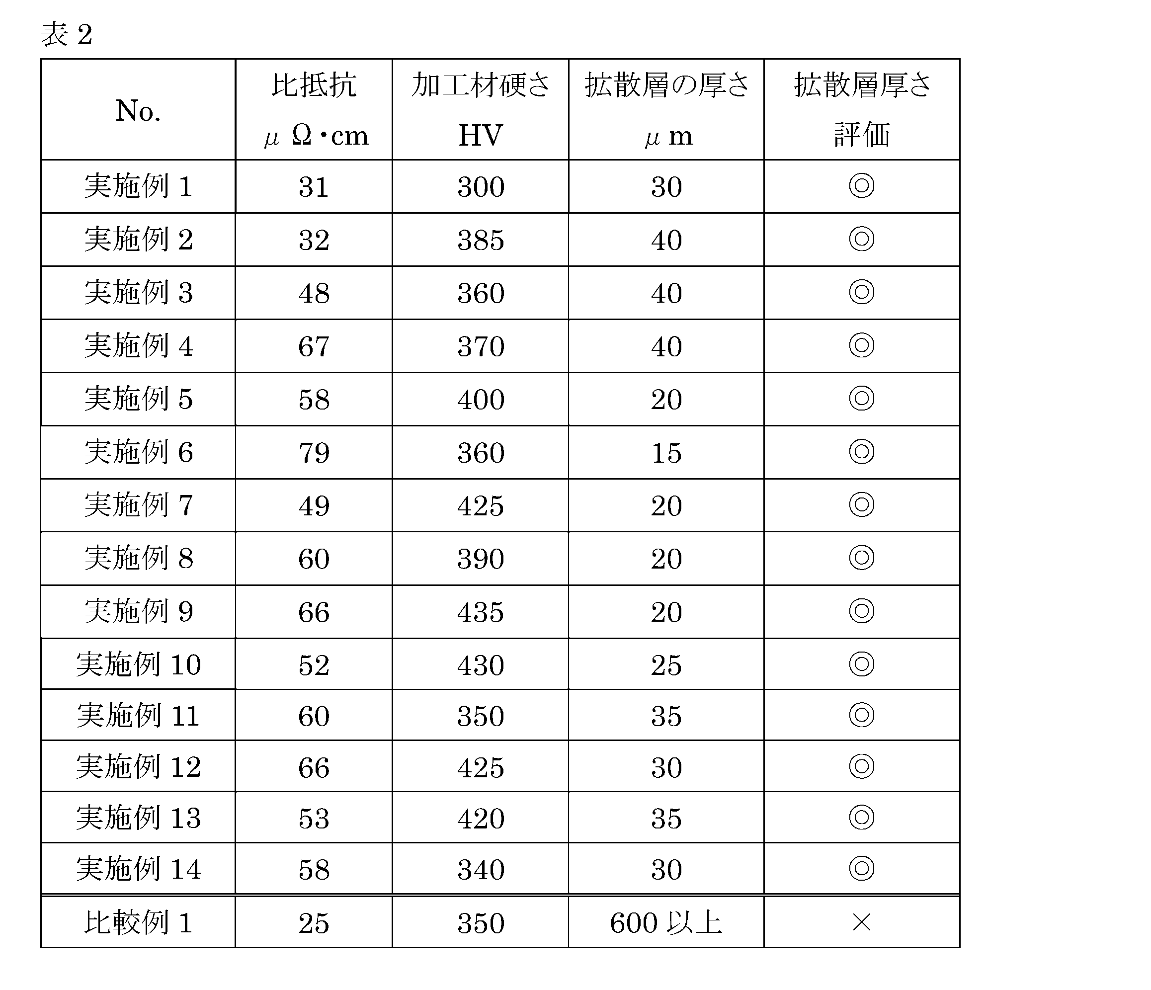
本発明により作製した合金は、高い耐はんだ性を有しつつ、プローブ材に求められる硬さ、比抵抗を併せ持つことが分かる。よって、本発明によって、耐はんだ性を有するプローブ材として好適な材料を提供することが可能となる。
Claims (1)
- Pt 40~95mass%、Cu 0.5~50mass%、Ni 3~50mass%からなることを特徴とするプローブピン用合金材料。
Priority Applications (3)
| Application Number | Priority Date | Filing Date | Title |
|---|---|---|---|
| KR1020257007291A KR20250053083A (ko) | 2022-09-07 | 2023-08-31 | 프로브 핀용 합금 재료 |
| CN202380060597.6A CN119744353A (zh) | 2022-09-07 | 2023-08-31 | 探测针用合金材料 |
| US19/109,069 US20260085383A1 (en) | 2022-09-07 | 2023-08-31 | Alloy material for probe pins |
Applications Claiming Priority (2)
| Application Number | Priority Date | Filing Date | Title |
|---|---|---|---|
| JP2022141820A JP2024037196A (ja) | 2022-09-07 | 2022-09-07 | プローブピン用合金材料 |
| JP2022-141820 | 2022-09-07 |
Publications (1)
| Publication Number | Publication Date |
|---|---|
| WO2024053552A1 true WO2024053552A1 (ja) | 2024-03-14 |
Family
ID=90191045
Family Applications (1)
| Application Number | Title | Priority Date | Filing Date |
|---|---|---|---|
| PCT/JP2023/031796 Ceased WO2024053552A1 (ja) | 2022-09-07 | 2023-08-31 | プローブピン用合金材料 |
Country Status (6)
| Country | Link |
|---|---|
| US (1) | US20260085383A1 (ja) |
| JP (1) | JP2024037196A (ja) |
| KR (1) | KR20250053083A (ja) |
| CN (1) | CN119744353A (ja) |
| TW (1) | TW202424217A (ja) |
| WO (1) | WO2024053552A1 (ja) |
Cited By (1)
| Publication number | Priority date | Publication date | Assignee | Title |
|---|---|---|---|---|
| CN120575067A (zh) * | 2025-08-04 | 2025-09-02 | 浙江金连接科技股份有限公司 | 一种芯片测试探针用高导电率钯合金及其制备方法 |
Citations (8)
| Publication number | Priority date | Publication date | Assignee | Title |
|---|---|---|---|---|
| JPS5970740A (ja) * | 1982-10-15 | 1984-04-21 | Tanaka Kikinzoku Kogyo Kk | 刷子用摺動接点材料 |
| JP2002270654A (ja) * | 2001-03-13 | 2002-09-20 | Kanai Hiroaki | プローブカード用プローブピン |
| JP2003149267A (ja) * | 2001-11-07 | 2003-05-21 | Sumitomo Electric Ind Ltd | 半導体素子の電気、電子特性測定用端子およびその製造方法 |
| JP2010054496A (ja) * | 2008-08-28 | 2010-03-11 | Samsung Electro-Mechanics Co Ltd | プローブカード及びその製造方法 |
| WO2012077378A1 (ja) * | 2010-12-09 | 2012-06-14 | 株式会社徳力本店 | 電気・電子用材 |
| JP2021113800A (ja) * | 2019-12-18 | 2021-08-05 | 株式会社クオルテック | 半導体試験装置及び半導体素子の試験方法 |
| JP2022151628A (ja) * | 2021-03-26 | 2022-10-07 | 株式会社ヨコオ | プローブ |
| JP2022151627A (ja) * | 2021-03-26 | 2022-10-07 | 石福金属興業株式会社 | プローブピン用合金材料 |
Family Cites Families (1)
| Publication number | Priority date | Publication date | Assignee | Title |
|---|---|---|---|---|
| US1935897A (en) | 1929-01-28 | 1933-11-21 | Int Nickel Co | Precious metal alloy |
-
2022
- 2022-09-07 JP JP2022141820A patent/JP2024037196A/ja active Pending
-
2023
- 2023-08-31 TW TW112132989A patent/TW202424217A/zh unknown
- 2023-08-31 WO PCT/JP2023/031796 patent/WO2024053552A1/ja not_active Ceased
- 2023-08-31 US US19/109,069 patent/US20260085383A1/en active Pending
- 2023-08-31 CN CN202380060597.6A patent/CN119744353A/zh active Pending
- 2023-08-31 KR KR1020257007291A patent/KR20250053083A/ko active Pending
Patent Citations (8)
| Publication number | Priority date | Publication date | Assignee | Title |
|---|---|---|---|---|
| JPS5970740A (ja) * | 1982-10-15 | 1984-04-21 | Tanaka Kikinzoku Kogyo Kk | 刷子用摺動接点材料 |
| JP2002270654A (ja) * | 2001-03-13 | 2002-09-20 | Kanai Hiroaki | プローブカード用プローブピン |
| JP2003149267A (ja) * | 2001-11-07 | 2003-05-21 | Sumitomo Electric Ind Ltd | 半導体素子の電気、電子特性測定用端子およびその製造方法 |
| JP2010054496A (ja) * | 2008-08-28 | 2010-03-11 | Samsung Electro-Mechanics Co Ltd | プローブカード及びその製造方法 |
| WO2012077378A1 (ja) * | 2010-12-09 | 2012-06-14 | 株式会社徳力本店 | 電気・電子用材 |
| JP2021113800A (ja) * | 2019-12-18 | 2021-08-05 | 株式会社クオルテック | 半導体試験装置及び半導体素子の試験方法 |
| JP2022151628A (ja) * | 2021-03-26 | 2022-10-07 | 株式会社ヨコオ | プローブ |
| JP2022151627A (ja) * | 2021-03-26 | 2022-10-07 | 石福金属興業株式会社 | プローブピン用合金材料 |
Cited By (1)
| Publication number | Priority date | Publication date | Assignee | Title |
|---|---|---|---|---|
| CN120575067A (zh) * | 2025-08-04 | 2025-09-02 | 浙江金连接科技股份有限公司 | 一种芯片测试探针用高导电率钯合金及其制备方法 |
Also Published As
| Publication number | Publication date |
|---|---|
| JP2024037196A (ja) | 2024-03-19 |
| CN119744353A (zh) | 2025-04-01 |
| TW202424217A (zh) | 2024-06-16 |
| US20260085383A1 (en) | 2026-03-26 |
| KR20250053083A (ko) | 2025-04-21 |
Similar Documents
| Publication | Publication Date | Title |
|---|---|---|
| EP2159581B1 (en) | Method of manufacturing probe pins | |
| US8183877B2 (en) | Material for probe pins | |
| JP7766290B2 (ja) | プローブピン用合金材料 | |
| JP2022041921A (ja) | パラジウム-銅-銀-ルテニウム合金 | |
| JP6728057B2 (ja) | 合金材料、コンタクトプローブおよび接続端子 | |
| TWI794355B (zh) | 析出硬化型Ag-Pd-Cu-In-B系合金 | |
| KR101260135B1 (ko) | 접촉저항, 방오특성이 우수한 프로브 핀 | |
| WO2024053552A1 (ja) | プローブピン用合金材料 | |
| WO2023189160A1 (ja) | プローブピン用合金材料 | |
| JP6372952B2 (ja) | Pt基合金で構成されるプローブピン用材料、プローブピンの製造方法 | |
| WO2022202681A1 (ja) | プローブピン用合金材料 | |
| JP7429011B2 (ja) | プローブピン用材料およびプローブピン | |
| JP2019026921A (ja) | 電気・電子機器用Cu合金及びそれを用いたプローブピン | |
| CN117015625A (zh) | 探测针用合金材料 | |
| JP2024089037A (ja) | プローブピン用合金材料 |
Legal Events
| Date | Code | Title | Description |
|---|---|---|---|
| 121 | Ep: the epo has been informed by wipo that ep was designated in this application |
Ref document number: 23863090 Country of ref document: EP Kind code of ref document: A1 |
|
| WWE | Wipo information: entry into national phase |
Ref document number: 202380060597.6 Country of ref document: CN |
|
| ENP | Entry into the national phase |
Ref document number: 20257007291 Country of ref document: KR Kind code of ref document: A |
|
| WWP | Wipo information: published in national office |
Ref document number: 202380060597.6 Country of ref document: CN |
|
| NENP | Non-entry into the national phase |
Ref country code: DE |
|
| WWP | Wipo information: published in national office |
Ref document number: 1020257007291 Country of ref document: KR |
|
| 122 | Ep: pct application non-entry in european phase |
Ref document number: 23863090 Country of ref document: EP Kind code of ref document: A1 |