WO2024053453A1 - Multi-level inverter - Google Patents
Multi-level inverter Download PDFInfo
- Publication number
- WO2024053453A1 WO2024053453A1 PCT/JP2023/030965 JP2023030965W WO2024053453A1 WO 2024053453 A1 WO2024053453 A1 WO 2024053453A1 JP 2023030965 W JP2023030965 W JP 2023030965W WO 2024053453 A1 WO2024053453 A1 WO 2024053453A1
- Authority
- WO
- WIPO (PCT)
- Prior art keywords
- voltage
- switching element
- gate drivers
- voltage vector
- vector
- Prior art date
Links
- 239000013598 vector Substances 0.000 claims abstract description 838
- 239000003990 capacitor Substances 0.000 claims description 190
- 230000003247 decreasing effect Effects 0.000 claims 2
- 230000015572 biosynthetic process Effects 0.000 abstract 1
- 238000003786 synthesis reaction Methods 0.000 abstract 1
- 238000010586 diagram Methods 0.000 description 34
- 230000000052 comparative effect Effects 0.000 description 20
- 239000002131 composite material Substances 0.000 description 8
- 238000001514 detection method Methods 0.000 description 8
- 230000003071 parasitic effect Effects 0.000 description 8
- 230000002457 bidirectional effect Effects 0.000 description 6
- 238000000034 method Methods 0.000 description 6
- 230000007423 decrease Effects 0.000 description 4
- 238000007599 discharging Methods 0.000 description 4
- 238000006243 chemical reaction Methods 0.000 description 2
- 230000006870 function Effects 0.000 description 2
- 230000004048 modification Effects 0.000 description 2
- 238000012986 modification Methods 0.000 description 2
- 230000003287 optical effect Effects 0.000 description 2
- 239000004065 semiconductor Substances 0.000 description 2
- 238000005516 engineering process Methods 0.000 description 1
- 239000007787 solid Substances 0.000 description 1
Images


Classifications
-
- H—ELECTRICITY
- H02—GENERATION; CONVERSION OR DISTRIBUTION OF ELECTRIC POWER
- H02M—APPARATUS FOR CONVERSION BETWEEN AC AND AC, BETWEEN AC AND DC, OR BETWEEN DC AND DC, AND FOR USE WITH MAINS OR SIMILAR POWER SUPPLY SYSTEMS; CONVERSION OF DC OR AC INPUT POWER INTO SURGE OUTPUT POWER; CONTROL OR REGULATION THEREOF
- H02M1/00—Details of apparatus for conversion
- H02M1/08—Circuits specially adapted for the generation of control voltages for semiconductor devices incorporated in static converters
-
- H—ELECTRICITY
- H02—GENERATION; CONVERSION OR DISTRIBUTION OF ELECTRIC POWER
- H02M—APPARATUS FOR CONVERSION BETWEEN AC AND AC, BETWEEN AC AND DC, OR BETWEEN DC AND DC, AND FOR USE WITH MAINS OR SIMILAR POWER SUPPLY SYSTEMS; CONVERSION OF DC OR AC INPUT POWER INTO SURGE OUTPUT POWER; CONTROL OR REGULATION THEREOF
- H02M7/00—Conversion of ac power input into dc power output; Conversion of dc power input into ac power output
- H02M7/42—Conversion of dc power input into ac power output without possibility of reversal
- H02M7/44—Conversion of dc power input into ac power output without possibility of reversal by static converters
- H02M7/48—Conversion of dc power input into ac power output without possibility of reversal by static converters using discharge tubes with control electrode or semiconductor devices with control electrode
- H02M7/483—Converters with outputs that each can have more than two voltages levels
- H02M7/487—Neutral point clamped inverters
Definitions
- the present disclosure relates to a multilevel inverter, and more particularly, to a multilevel inverter with a bootstrap circuit.
- Patent Document 1 discloses a three-phase voltage type PWM inverter circuit using a bootstrap circuit.
- the three-phase voltage type PWM inverter circuit disclosed in Patent Document 1 includes six switching elements, six gate drive circuits, a microcomputer, a main DC power supply, and three bootstrap circuits. are doing.
- Patent Document 1 discloses that by giving a predetermined switching pattern to each phase of a three-phase inverter, a desired voltage vector is obtained and supplied to the load, and a control voltage is supplied by a bootstrap circuit for each phase.
- An inverter control method is disclosed.
- the bootstrap circuit can charge a voltage vector selected during a period that does not affect the output voltage within a period in which the bootstrap circuit of any phase maintains a discharged state at predetermined intervals. Switching control is performed to replace it with a voltage vector.
- Patent Document 1 is a technology related to a two-level inverter, and does not disclose a control method for a multi-level inverter.
- An object of the present disclosure is to provide a multilevel inverter that can suppress voltage drop in a bootstrap circuit.
- a multilevel inverter includes a DC power supply section, a plurality of inverter circuits, and a control device.
- the DC power supply section has a positive electrode, a negative electrode, and an intermediate potential point.
- the plurality of inverter circuits are connected between the positive electrode and the negative electrode of the DC power supply section.
- the control device controls the plurality of inverter circuits.
- Each of the plurality of inverter circuits includes a switching circuit, a first diode, a second diode, a third diode, a fourth diode, a fifth diode, and a sixth diode.
- the first switching element, the second switching element, the third switching element, and the fourth switching element are connected from the positive electrode side to the negative electrode side.
- the element and the fourth switching element are connected in series so as to be lined up in this order.
- the first diode is connected in antiparallel to the first switching element.
- the second diode is connected in antiparallel to the second switching element.
- the third diode is connected in antiparallel to the third switching element.
- the fourth diode is connected in antiparallel to the fourth switching element.
- the fifth diode has a cathode connected to a first connection point between the first switching element and the second switching element, and an anode connected to the intermediate potential point.
- the sixth diode has an anode connected to a second connection point between the third switching element and the fourth switching element, and a cathode connected to the intermediate potential point.
- the control device includes a plurality of first gate drivers, a plurality of second gate drivers, a plurality of third gate drivers, a plurality of fourth gate drivers, a plurality of first bootstrap circuits, and a plurality of second gate drivers. It has a bootstrap circuit, a plurality of third bootstrap circuits, a power supply section, and a control section.
- the plurality of first gate drivers drive the first switching elements of each of the plurality of inverter circuits.
- the plurality of second gate drivers drive the second switching elements of each of the plurality of inverter circuits.
- the plurality of third gate drivers drive the third switching elements of each of the plurality of inverter circuits.
- the plurality of fourth gate drivers drive the fourth switching elements of each of the plurality of inverter circuits.
- the plurality of first bootstrap circuits correspond one-to-one to the plurality of first gate drivers. Each of the plurality of first bootstrap circuits supplies a voltage to a corresponding first gate driver.
- the plurality of second bootstrap circuits correspond one-to-one to the plurality of second gate drivers. Each of the plurality of second bootstrap circuits supplies a voltage to a corresponding second gate driver.
- the plurality of third bootstrap circuits correspond one-to-one to the plurality of third gate drivers.
- Each of the plurality of third bootstrap circuits supplies a voltage to a corresponding third gate driver.
- the power supply unit supplies voltage to the plurality of fourth gate drivers.
- the control unit controls the plurality of first gate drivers, the plurality of second gate drivers, the plurality of third gate drivers, and the plurality of fourth gate drivers.
- the control unit selects a first voltage vector, a second voltage vector, and a third voltage vector adjacent to the command voltage vector from among the first group of voltage vectors.
- Each of the first group of voltage vectors is determined by a combination of potential levels at a third connection point between the second switching element and the third switching element of the plurality of inverter circuits in the first vector space.
- the control unit converts the first voltage vector, the second voltage vector, and the third voltage vector into a second group of voltage vectors in a second vector space different from the first vector space.
- the combination is changed to a zero vector and a fourth voltage vector and a fifth voltage vector adjacent to the command voltage vector.
- Each of the second group of voltage vectors is determined by a combination of potential levels at a third connection point between the second switching element and the third switching element of the plurality of inverter circuits.
- the zero vector is a combination of voltage vectors of the second group in which the potential level of the third connection point between the second switching element and the third switching element of the plurality of inverter circuits is the potential of the negative electrode. , and a voltage vector of a combination that becomes the potential of the positive electrode.
- the control unit is configured within a predetermined control period to match a composite vector of the zero vector, the fourth voltage vector, and the fifth voltage vector in the second vector space with the command voltage vector.
- the plurality of first gate drivers, the plurality of second gate drivers, the plurality of third gate drivers, and the plurality of fourth gate drivers are controlled.
- a multilevel inverter includes a DC power supply section, a plurality of inverter circuits, and a control device.
- the DC power supply section has a positive electrode, a negative electrode, and an intermediate potential point.
- the plurality of inverter circuits are connected between the positive electrode and the negative electrode of the DC power supply section.
- the control device controls the plurality of inverter circuits.
- Each of the plurality of inverter circuits includes a first switching element, a second switching element, a third switching element, a fourth switching element, and a first diode, a second diode, a third diode, and a fourth diode.
- the first diode, the second diode, the third diode, and the fourth diode are connected in antiparallel to the first switching element, the second switching element, the third switching element, and the fourth switching element, respectively. ing.
- the first switching element and the second switching element are connected in series such that the first switching element and the second switching element are arranged in this order from the positive electrode side to the negative electrode side.
- a series circuit of the third switching element and the fourth switching element is connected between the intermediate potential point and the output point.
- the output point is a connection point between the first switching element and the second switching element.
- the control device includes a plurality of first gate drivers, a plurality of second gate drivers, a plurality of third gate drivers, a plurality of fourth gate drivers, a plurality of bootstrap circuits, a power supply section, and a control section. and has.
- the plurality of first gate drivers drive the first switching elements of each of the plurality of inverter circuits.
- the plurality of second gate drivers drive the second switching elements of each of the plurality of inverter circuits.
- the plurality of third gate drivers drive the third switching elements of each of the plurality of inverter circuits.
- the plurality of fourth gate drivers drive the fourth switching elements of each of the plurality of inverter circuits.
- the plurality of bootstrap circuits correspond one-to-one to the plurality of first gate drivers, and supply voltage to the corresponding first gate drivers.
- the power supply unit supplies voltage to the plurality of second gate drivers and the plurality of third gate drivers.
- the control unit controls the plurality of first gate drivers, the plurality of second gate drivers, the plurality of third gate drivers, and the plurality of fourth gate drivers.
- the control unit selects a first voltage vector, a second voltage vector, and a third voltage vector adjacent to the command voltage vector from among the first group of voltage vectors.
- Each of the first group of voltage vectors is determined by a combination of potential levels of the plurality of connection points in the plurality of inverter circuits in the first vector space.
- the control unit converts the first voltage vector, the second voltage vector, and the third voltage vector into a second group of voltage vectors in a second vector space different from the first vector space.
- the combination is changed to a zero vector and a fourth voltage vector and a fifth voltage vector adjacent to the command voltage vector.
- Each of the second group of voltage vectors is determined by a combination of potential levels of the plurality of connection points in the plurality of inverter circuits.
- the zero vector is a combination of voltage vectors among the second group of voltage vectors in which the potential level of the plurality of connection points in the plurality of inverter circuits becomes the potential of the negative electrode, and a combination of voltage vectors in which the potential level of the plurality of connection points in the plurality of inverter circuits becomes the potential of the positive electrode. It is a voltage vector.
- the control unit is configured within a predetermined control period to match a composite vector of the zero vector, the fourth voltage vector, and the fifth voltage vector in the second vector space with the command voltage vector. In the method, the plurality of first gate drivers, the plurality of second gate drivers, the plurality of third gate drivers, and the plurality of fourth gate drivers are controlled.
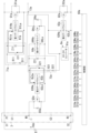
- FIG. 1 is a circuit diagram of a system including a multilevel inverter according to a first embodiment.
- FIG. 2 is an explanatory diagram of the current path when the switching circuit is in the first switching state in the multilevel inverter same as above.
- FIG. 3 is an explanatory diagram of a discharging path and a charging path when the switching circuit is in the first switching state in the multilevel inverter same as above.
- FIG. 4 is an explanatory diagram of the current path when the switching circuit is in the second switching state in the above multilevel inverter.
- FIG. 5 is an explanatory diagram of a discharging path and a charging path when the switching circuit is in the second switching state in the multilevel inverter same as above.
- FIG. 6 is an explanatory diagram of the current path when the switching circuit is in the third switching state in the multilevel inverter same as above.
- FIG. 7 is an explanatory diagram of the discharging path and the charging path when the switching circuit is in the third switching state in the multilevel inverter same as above.
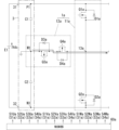
- FIG. 8 is an explanatory diagram of voltage command values for each phase in the multilevel inverter same as above.
- FIG. 9 is an explanatory diagram of the first group of voltage vectors regarding the multilevel inverter same as above.
- FIG. 10 is a more detailed explanatory diagram of the first group of voltage vectors regarding the multilevel inverter.
- FIG. 11 is a vector diagram for explaining the operation of the control section in the multilevel inverter.
- FIG. 12A is an explanatory diagram of a command voltage vector, a first voltage vector, a second voltage vector, and a third voltage vector regarding the multilevel inverter.
- FIG. 12B is an explanatory diagram of a command voltage vector, a zero vector, a fourth voltage vector, and a fifth voltage vector regarding the multilevel inverter.
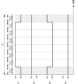
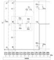
- FIG. 13 is a time chart of the switching state of each phase of the multilevel inverter according to the comparative example.
- FIG. 14 is a time chart of the on/off states of the first to fourth switching elements of the multilevel inverter according to the comparative example.
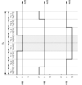
- FIG. 15 shows that in the multilevel inverter according to the first embodiment, the combination of the first voltage vector, the second voltage vector, and the third voltage vector is changed to the combination of the zero vector, the fourth voltage vector, and the fifth voltage vector. It is a time chart of the switching state of each phase when the inverter circuit of each phase is controlled.
- FIG. 16 shows how to control the inverter circuit by changing the combination of the first voltage vector, the second voltage vector, and the third voltage vector to the combination of the zero vector, the fourth voltage vector, and the fifth voltage vector in the same multilevel inverter as above.
- 12 is a time chart of the on/off states of the first to fourth switching elements in the case of FIG. FIG.
- FIG. 17 is a time chart of the switching states of each phase of the multilevel inverter according to the comparative example.
- FIG. 18 is a time chart of the on/off states of the first to fourth switching elements of the multilevel inverter according to the comparative example.
- FIG. 19 shows that in the multilevel inverter according to Embodiment 1, the combination of the first voltage vector, the second voltage vector, and the third voltage vector is changed to the combination of the zero vector, the fourth voltage vector, and the fifth voltage vector. It is a time chart of the switching state of each phase when the inverter circuit of each phase is controlled.
- FIG. 20 shows how to control the inverter circuit by changing the combination of the first voltage vector, the second voltage vector, and the third voltage vector to the combination of the zero vector, the fourth voltage vector, and the fifth voltage vector in the same multilevel inverter as above.
- 12 is a time chart of the on/off states of the first to fourth switching elements in the case of FIG.
- FIG. 21 is a circuit diagram of a system including a multilevel inverter according to a modification.
- FIG. 22 is a circuit diagram of a system including a multilevel inverter according to the second embodiment.
- FIG. 23 is an explanatory diagram of the current path when the switching circuit is in the first switching state in the multilevel inverter same as above.
- FIG. 24 is an explanatory diagram of the discharge path when the switching circuit is in the first switching state in the above multilevel inverter.
- FIG. 25 is an explanatory diagram of the current path when the switching circuit is in the second switching state in the multilevel inverter same as above.
- FIG. 26 is an explanatory diagram of the discharge path when the switching circuit is in the second switching state in the above multilevel inverter.
- FIG. 27 is an explanatory diagram of the current path when the switching circuit is in the third switching state in the multilevel inverter same as above.
- FIG. 28 is an explanatory diagram of the discharging path and the charging path when the switching circuit is in the third switching state in the multilevel inverter same as above.
- FIG. 29 is an explanatory diagram of the discharge path when the switching circuit is in the second switching state in the multilevel inverter same as above.
- FIG. 30 is an explanatory diagram of voltage command values for each phase in the multilevel inverter same as above.
- FIG. 31 is an explanatory diagram of the first group of voltage vectors regarding the multilevel inverter same as above.
- FIG. 32 is a more detailed explanatory diagram of the first group of voltage vectors regarding the multilevel inverter.
- FIG. 33 is a vector diagram for explaining the operation of the control section in the multilevel inverter.
- FIG. 34A is an explanatory diagram of a command voltage vector, a first voltage vector, a second voltage vector, and a third voltage vector regarding the multilevel inverter same as above.
- FIG. 34B is an explanatory diagram of a command voltage vector, a zero vector, a fourth voltage vector, and a fifth voltage vector regarding the same multilevel inverter.
- FIG. 35 is a time chart of the switching state of each phase of the multilevel inverter according to the comparative example.
- FIG. 36 is a time chart of the on/off states of the first to fourth switching elements of the multilevel inverter according to the comparative example.
- FIG. 37 shows that in the multilevel inverter according to the second embodiment, the combination of the first voltage vector, the second voltage vector, and the third voltage vector is changed to the combination of the zero vector, the fourth voltage vector, and the fifth voltage vector. It is a time chart of the switching state of each phase when the inverter circuit of each phase is controlled.
- FIG. 35 is a time chart of the switching state of each phase of the multilevel inverter according to the comparative example.
- FIG. 36 is a time chart of the on/off states of the first to fourth switching elements of the multilevel in
- FIG. 38 shows how to control the inverter circuit by changing the combination of the first voltage vector, the second voltage vector, and the third voltage vector to the combination of the zero vector, the fourth voltage vector, and the fifth voltage vector in the same multilevel inverter as above.
- 12 is a time chart of the on/off states of the first to fourth switching elements in the case of the present invention.
- FIG. 39 is a time chart of the switching state of each phase of the multilevel inverter according to the comparative example.
- FIG. 40 is a time chart of the on/off states of the first to fourth switching elements of the multilevel inverter according to the comparative example.
- FIG. 41 shows that in the multilevel inverter according to the second embodiment, the combination of the first voltage vector, the second voltage vector, and the third voltage vector is changed to the combination of the zero vector, the fourth voltage vector, and the fifth voltage vector. It is a time chart of the switching state of each phase when the inverter circuit of each phase is controlled.
- FIG. 42 shows how to control the inverter circuit by changing the combination of the first voltage vector, the second voltage vector, and the third voltage vector to the combination of the zero vector, the fourth voltage vector, and the fifth voltage vector in the same multilevel inverter as above.
- 12 is a time chart of the on/off states of the first to fourth switching elements in the case of FIG.
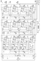
- FIG. 43 is a circuit diagram of a system including a multilevel inverter according to the third embodiment.
- FIG. 44 is a circuit diagram of a system including a multilevel inverter according to the fourth embodiment.
- FIG. 45 is a circuit diagram of a system including a multilevel inverter according to the fifth embodiment.
- FIG. 46 is a circuit diagram of a system including a multilevel inverter according to the sixth embodiment.
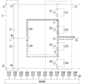
- the multilevel inverter 100 includes, for example, as shown in FIG. 1, a DC power supply section 3, a plurality of (for example, three) inverter circuits 1, and a control device 6.
- the DC power supply section 3 has a positive electrode P1, a negative electrode N1, and an intermediate potential point M1.
- the plurality of inverter circuits 1 are connected between the positive electrode P1 and the negative electrode N1 of the DC power supply section 3.
- the control device 6 controls the plurality of inverter circuits 1.
- the multilevel inverter 100 is a diode clamp type three-level, three-phase inverter.
- each of the plurality of inverter circuits 1 has an output terminal 41.
- an AC load RA1 is connected to a plurality of output terminals (AC terminals) 41.
- AC load RA1 is, for example, a three-phase motor.
- one of the plurality of inverter circuits 1 is an inverter circuit 1U that outputs a U-phase voltage
- another one is an inverter circuit 1V that outputs a V-phase voltage
- the remaining One is an inverter circuit 1W that outputs a W-phase voltage.
- Each of the plurality of inverter circuits 1 includes a switching circuit 10, a first diode D1, a second diode D2, a third diode D3, and a fourth diode D4. Moreover, each of the plurality of inverter circuits 1 includes a fifth diode D5 and a sixth diode D6. In the multilevel inverter 100, the potential at the intermediate potential point M1 is clamped by the fifth diode D5 and the sixth diode D6 of each inverter circuit 1.
- the first switching element Q1, the second switching element Q2, the third switching element Q3, and the fourth switching element Q4 are connected from the positive electrode P1 side of the DC power supply section 3 to the negative electrode N1 side of the first switching element Q1,
- the second switching element Q2, the third switching element Q3, and the fourth switching element Q4 are connected in series in this order.
- the first diode D1 is connected in antiparallel to the first switching element Q1.
- the second diode D2 is connected in antiparallel to the second switching element Q2.
- the third diode D3 is connected in antiparallel to the third switching element Q3.
- the fourth diode D4 is connected in antiparallel to the fourth switching element Q4.
- the fifth diode D5 has a cathode connected to the first connection point 11 between the first switching element Q1 and the second switching element Q2, and an anode connected to the intermediate potential point M1.
- the sixth diode D6 has an anode connected to the second connection point 12 between the third switching element Q3 and the fourth switching element Q4, and a cathode connected to the intermediate potential point M1.
- the control device 6 includes a plurality of (for example, three) first gate drivers 61, a plurality of (for example, three) second gate drivers 62, a plurality of (for example, three) third gate drivers 63, A plurality of (for example, three) fourth gate drivers 64 are included.
- the control device 6 also includes a plurality of (for example, three) first bootstrap circuits 71, a plurality of (for example, three) second bootstrap circuits 72, and a plurality of (for example, three) third bootstrap circuits 71, and a plurality of (for example, three) third bootstrap circuits 71. It has a strap circuit 73, a power supply section 9, and a control section 60.
- the plurality of first gate drivers 61 drive the first switching elements Q1 of each of the plurality of inverter circuits 1.
- the plurality of second gate drivers 62 drive the second switching elements Q2 of each of the plurality of inverter circuits 1.
- the plurality of third gate drivers 63 drive each third switching element Q3 of the plurality of inverter circuits 1.
- the plurality of fourth gate drivers 64 drive the fourth switching elements Q4 of each of the plurality of inverter circuits 1.
- the plurality of first bootstrap circuits 71 correspond to the plurality of first gate drivers 61 on a one-to-one basis. Each of the plurality of first bootstrap circuits 71 supplies a voltage to the corresponding first gate driver 61.
- the plurality of second bootstrap circuits 72 correspond to the plurality of second gate drivers 62 on a one-to-one basis. Each of the plurality of second bootstrap circuits 72 supplies a voltage to the corresponding second gate driver 62.
- the plurality of third bootstrap circuits 73 correspond to the plurality of third gate drivers 63 on a one-to-one basis. Each of the plurality of third bootstrap circuits 73 supplies voltage to the corresponding third gate driver 63.
- the power supply section 9 supplies voltage to the plurality of fourth gate drivers 64.
- the control unit 60 controls a plurality of first gate drivers 61 , a plurality of second gate drivers 62 , a plurality of third gate drivers 63 , and a plurality of fourth gate drivers 64 .
- the DC power supply unit 3 includes a first capacitor C1 and a second capacitor C2.
- a first capacitor C1 and a second capacitor C2 are connected in series.
- the DC power supply section 3 further includes a first DC terminal 31 connected to the positive electrode P1 and a second DC terminal 32 connected to the negative electrode N1.
- the first end of the first capacitor C1 is connected to the first DC terminal 31
- the second end of the first capacitor C1 is connected to the first end of the second capacitor C2
- the first end of the first capacitor C1 is connected to the first end of the second capacitor C2.
- the second end of the two capacitor C2 is connected to the second DC terminal 32.
- the connection point between the first capacitor C1 and the second capacitor C2 is an intermediate potential point M1.
- a DC voltage source E1 is connected between the first DC terminal 31 and the second DC terminal 32.
- the output voltage Vdc of the DC voltage source E1 is applied between the positive pole P1 and the negative pole N1 of the DC power supply section 3.
- the capacitance of the second capacitor C2 is the same as that of the first capacitor C1.
- the capacitance of the second capacitor C2 is the same as the capacitance of the first capacitor C1" is not limited to the case where the capacitance of the second capacitor C2 completely matches the capacitance of the first capacitor C1; It is sufficient that the capacitance of C2 is within the range of 95% or more and 105% or less of the capacitance of the first capacitor C1.
- the switching circuit 10 included in the inverter circuit 1U will be referred to as the switching circuit 10U
- the switching circuit 10 included in the inverter circuit 1V will be referred to as the switching circuit 10V
- the switching circuit 10 included in the inverter circuit 1W will be referred to as the switching circuit 10V
- the included switching circuit 10 may also be referred to as a switching circuit 10W.
- the output terminal 41 included in the inverter circuit 1U is referred to as an output terminal 41U
- the output terminal 41 included in the inverter circuit 1V is referred to as an output terminal 41V
- the output terminal 41 included in the inverter circuit 1W is referred to as an output terminal 41V. is sometimes referred to as the output terminal 41W.
- the first switching element Q1, the second switching element Q2, the third switching element Q3, and the fourth switching element Q4 of each switching circuit 10 have a control terminal, a first main terminal, and a second main terminal.
- the first switching element Q1, the second switching element Q2, the third switching element Q3, and the fourth switching element Q4 of each switching circuit 10 are, for example, MOSFETs. Therefore, the control terminal, the first main terminal, and the second main terminal of each of the first switching element Q1, the second switching element Q2, the third switching element Q3, and the fourth switching element Q4 of each switching circuit 10 are as follows. These are a gate terminal, a drain terminal, and a source terminal.
- the MOSFETs forming each of the first switching element Q1, the second switching element Q2, the third switching element Q3, and the fourth switching element Q4 are, for example, normally-off type n-channel MOSFETs.
- the MOSFET is, for example, a Si-based MOSFET or a SiC-based MOSFET.
- the control terminal of the first switching element Q1 of each switching circuit 10 is connected to the corresponding first gate driver 61 among the plurality of first gate drivers 61. Further, a control terminal of the second switching element Q2 of each switching circuit 10 is connected to a corresponding second gate driver 62 among the plurality of second gate drivers 62. Further, the control terminal of the third switching element Q3 of each switching circuit 10 is connected to a corresponding third gate driver 63 among the plurality of third gate drivers 63. Further, a control terminal of the fourth switching element Q4 of each switching circuit 10 is connected to a corresponding fourth gate driver 64 among the plurality of fourth gate drivers 64.
- the first main terminal of the first switching element Q1 is connected to the positive electrode P1 of the DC power supply section 3, and the second main terminal of the first switching element Q1 is connected to the first main terminal of the second switching element Q2. It is connected. Furthermore, in each switching circuit 10, the second main terminal of the second switching element Q2 is connected to the first main terminal of the third switching element Q3. In each switching circuit 10, the second main terminal of the third switching element Q3 is connected to the first main terminal of the fourth switching element Q4, and the second main terminal of the fourth switching element Q4 is connected to the negative terminal of the DC power supply section 3. Connected to N1.
- the third connection point 13 between the second switching element Q2 and the third switching element Q3 in the switching circuit 10U is connected to the output terminal 41U. Further, in the inverter circuit 1V, the third connection point 13 between the second switching element Q2 and the third switching element Q3 in the switching circuit 10V is connected to the output terminal 41V. Further, in the inverter circuit 1W, the third connection point 13 between the second switching element Q2 and the third switching element Q3 in the switching circuit 10W is connected to the output terminal 41W.
- the U phase of the AC load RA1 is connected to the third connection point 13 of the inverter circuit 1U via the output terminal 41U.
- the V phase of the AC load RA1 is connected to the third connection point 13 of the inverter circuit 1V via the output terminal 41V.
- the W phase of the AC load RA1 is connected to the third connection point 13 of the inverter circuit 1W via the output terminal 41W.
- the anode of the first diode D1 is connected to the second main terminal (source terminal) of the first switching element Q1, and the cathode of the first diode D1 is connected to the first main terminal of the first switching element Q1. (drain terminal). Furthermore, in each inverter circuit 1, the anode of the second diode D2 is connected to the second main terminal (source terminal) of the second switching element Q2, and the cathode of the second diode D2 is connected to the first main terminal of the second switching element Q2. Connected to the main terminal (drain terminal).
- the anode of the third diode D3 is connected to the second main terminal (source terminal) of the third switching element Q3, and the cathode of the third diode D3 is connected to the first main terminal of the third switching element Q3. Connected to the main terminal (drain terminal).
- the anode of the fourth diode D4 is connected to the second main terminal (source terminal) of the fourth switching element Q4, and the cathode of the fourth diode D4 is connected to the first main terminal of the fourth switching element Q4. Connected to the main terminal (drain terminal).
- the first diode D1 may be replaced by a parasitic diode of a MOSFET that constitutes the first switching element Q1.
- the second diode D2 may be replaced by a parasitic diode of a MOSFET that constitutes the second switching element Q2.
- the third diode D3 may be replaced by a parasitic diode of a MOSFET that constitutes the third switching element Q3.
- the fourth diode D4 may be replaced by a parasitic diode of a MOSFET that constitutes the fourth switching element Q4.
- the cathode of the fifth diode D5 is connected to the first connection point 11 between the first switching element Q1 and the second switching element Q2. Further, the anode of the fifth diode D5 is connected to the intermediate potential point M1 of the DC power supply section 3.
- the "intermediate potential point M1" is a point at which the potential is intermediate between the potential of the positive electrode P1 and the potential of the negative electrode N1 of the DC power supply unit 3.
- the intermediate potential point M1 is connected to the ground, so the potential of the intermediate potential point M1 is 0V. In this case, assuming that the voltage across the DC power supply section 3 is Vdc, the potential of the positive electrode P1 is Vdc/2, and the potential of the negative electrode N1 is -Vdc/2.
- the cathode of the sixth diode D6 is connected to the intermediate potential point M1.
- the anode of the sixth diode D6 is connected to the second connection point 12 between the third switching element Q3 and the fourth switching element Q4.
- the plurality of first gate drivers 61 correspond one-to-one to the plurality of first switching elements Q1.
- the plurality of first gate drivers 61 are connected to the control terminals of the corresponding first switching elements Q1.
- the plurality of first gate drivers 61 drive corresponding first switching elements Q1.
- the plurality of first gate drivers 61 are connected to the control section 60.
- the control unit 60 outputs a plurality of first control signals S1 (see FIG. 2) corresponding one-to-one to the plurality of first gate drivers 61.
- Each of the plurality of first gate drivers 61 controls on/off of the first switching element Q1 based on the applied first control signal S1.
- the plurality of second gate drivers 62 correspond one-to-one to the plurality of second switching elements Q2.
- the plurality of second gate drivers 62 are connected to the control terminals of the corresponding second switching elements Q2.
- the plurality of second gate drivers 62 drive corresponding second switching elements Q2.
- the plurality of second gate drivers 62 are connected to the control section 60.
- the control unit 60 outputs a plurality of second control signals S2 (see FIG. 2) corresponding one-to-one to the plurality of second gate drivers 62.
- Each of the plurality of second gate drivers 62 controls on/off of the second switching element Q2 based on the applied second control signal S2.
- the plurality of third gate drivers 63 correspond one-to-one to the plurality of third switching elements Q3.
- the plurality of third gate drivers 63 are connected to the control terminals of the corresponding third switching elements Q3.
- the plurality of third gate drivers 63 drive corresponding third switching elements Q3.
- the plurality of third gate drivers 63 are connected to the control section 60.
- the control unit 60 outputs a plurality of third control signals S3 (see FIG. 2) corresponding one-to-one to the plurality of third gate drivers 63.
- Each of the plurality of third gate drivers 63 controls on/off of the third switching element Q3 based on the applied third control signal S3.
- the plurality of fourth gate drivers 64 correspond one-to-one to the plurality of fourth switching elements Q4.
- the plurality of fourth gate drivers 64 are connected to the control terminals of the corresponding fourth switching elements Q4.
- the plurality of fourth gate drivers 64 drive corresponding fourth switching elements Q4.
- the plurality of fourth gate drivers 64 are connected to the control section 60.
- the control unit 60 outputs a plurality of fourth control signals S4 (see FIG. 2) corresponding one-to-one to the plurality of fourth gate drivers 64.
- Each of the plurality of fourth gate drivers 64 controls on/off of the fourth switching element Q4 based on the applied fourth control signal S4.
- the plurality of first bootstrap circuits 71 correspond to the plurality of first gate drivers 61 on a one-to-one basis.
- the plurality of first bootstrap circuits 71 supply voltage to the corresponding first gate drivers 61.
- Each of the plurality of first bootstrap circuits 71 includes a diode D17, a resistor R17, and a capacitor C17 (also referred to as a boost capacitor C17).
- the anode of the diode D17 is connected to the positive terminal of the power supply section 9, and the cathode of the diode D17 is connected to the first end of the capacitor C17 via the resistor R17.
- the first end of the capacitor C17 is connected to the high potential side power supply terminal 61H (see FIG.
- the first bootstrap circuit 71 supplies the first gate driver 61 with a voltage necessary to turn on the first switching element Q1 in the first gate driver 61.
- Each of the plurality of first bootstrap circuits 71 further includes a Zener diode Z17 connected in parallel to the capacitor C17.
- the plurality of second bootstrap circuits 72 correspond to the plurality of second gate drivers 62 on a one-to-one basis.
- the plurality of second bootstrap circuits 72 supply voltages to the corresponding second gate drivers 62.
- Each of the plurality of second bootstrap circuits 72 includes a diode D27, a resistor R27, and a capacitor C27 (also referred to as a boost capacitor C27).
- the anode of the diode D27 is connected to the positive terminal of the power supply section 9, and the cathode of the diode D27 is connected to the first end of the capacitor C27 via the resistor R27.
- the first end of the capacitor C27 is connected to the high potential side power supply terminal 62H (see FIG.
- the second bootstrap circuit 72 supplies the second gate driver 62 with a voltage necessary to turn on the second switching element Q2 in the second gate driver 62.
- Each of the plurality of second bootstrap circuits 72 further includes a Zener diode Z27 connected in parallel to the capacitor C27.
- the plurality of third bootstrap circuits 73 correspond to the plurality of third gate drivers 63 on a one-to-one basis.
- the plurality of third bootstrap circuits 73 supply voltage to the corresponding third gate drivers 63.
- Each of the plurality of third bootstrap circuits 73 includes a diode D37, a resistor R37, and a capacitor C37 (also referred to as a boost capacitor C37).
- the anode of the diode D37 is connected to the positive terminal of the power supply section 9, and the cathode of the diode D37 is connected to the first end of the capacitor C37 via the resistor R37.
- the first end of the capacitor C37 is connected to the high potential power supply terminal 63H (see FIG.
- the third bootstrap circuit 73 supplies the third gate driver 63 with a voltage necessary to turn on the third switching element Q3 in the third gate driver 63.
- Each of the plurality of third bootstrap circuits 73 further includes a Zener diode Z37 connected in parallel to the capacitor C37.
- the power supply section 9 includes a plurality (three) of first bootstrap circuits 71, a plurality (three) of second bootstrap circuits 72, a plurality (three) of third bootstrap circuits 73, and a plurality (three) of third bootstrap circuits 73.
- a voltage is supplied to the fourth gate driver 64.
- the power supply unit 9 is, for example, a DC power supply including an isolated DC-DC converter 91.
- the positive side terminal of the power supply unit 9 is connected to the high potential side power supply terminal 64H (see FIG. 3) of each of the plurality of fourth gate drivers 64, and the negative side terminal of the power supply unit 9 is connected to the high potential side power supply terminal 64H (see FIG. 3) of each of the plurality of fourth gate drivers 64. It is connected to the low potential side power supply terminal 64L (see FIG. 3) of each driver 64.
- the control unit 60 controls a plurality of first gate drivers 61 , a plurality of second gate drivers 62 , a plurality of third gate drivers 63 , and a plurality of fourth gate drivers 64 . Thereby, the control unit 60 controls the plurality of first switching elements Q1, the plurality of second switching elements Q2, the plurality of third switching elements Q3, and the plurality of fourth switching elements Q4.
- the main body that executes the control unit 60 includes a computer system.
- a computer system includes one or more computers.
- a computer system mainly consists of a processor and a memory as hardware.
- the function of the control unit 60 as an execution entity in the present disclosure is realized by the processor executing a program recorded in the memory of the computer system.
- the program may be pre-recorded in the computer system's memory, or may be provided via a telecommunications line, or may be stored in a non-temporary storage device such as a memory card, optical disk, hard disk drive (magnetic disk), etc. that can be read by the computer system. It may also be provided recorded on a digital recording medium.
- a processor of a computer system is composed of one or more electronic circuits including a semiconductor integrated circuit (IC) or a large-scale integrated circuit (LSI).
- the plurality of electronic circuits may be integrated into one chip, or may be provided in a distributed manner over a plurality of chips.
- a plurality of chips may be integrated into one device, or may be distributed and provided in a plurality of devices.
- the control unit 60 receives a plurality of (three) first control signals S1 (see FIG. 2) for controlling a plurality of (three) first switching elements Q1 and a plurality of (three) second switching elements Q2.
- a plurality of (three) second control signals S2 for controlling the plurality of third switching elements Q3, and a plurality of (three) third control signals S3 (see FIG. 2) for controlling the plurality of third switching elements Q3.
- a plurality of (three) fourth control signals S4 for controlling the plurality of (three) fourth switching elements Q4. Note that, in FIG. 2, only one inverter circuit 1 among the three inverter circuits 1 (see FIG. 1) is illustrated, and illustration of the remaining two inverter circuits 1 is omitted.
- FIG. 2 a plurality of first gate drivers 61, a plurality of second gate drivers 62, a plurality of third gate drivers 63, a plurality of fourth gate drivers 64, and a plurality of first gate drivers 61 in FIG.
- the illustration of the bootstrap circuit 71, the plurality of second bootstrap circuits 72, the plurality of third bootstrap circuits 73, and the power supply section 9 is omitted. Further, in FIG. 3, only one inverter circuit 1 among the three inverter circuits 1 (see FIG. 1) is illustrated, and illustration of the remaining two inverter circuits 1 is omitted. 3, two first gate drivers 61, two second gate drivers 62, two third gate drivers 63, two fourth gate drivers 64, and two first The illustration of the bootstrap circuit 71, two second bootstrap circuits 72, and two third bootstrap circuits 73 is omitted.
- the three first control signals S1 are a first control signal S1U that controls the first switching element Q1 of the switching circuit 10U, a first control signal S1V that controls the first switching element Q1 of the switching circuit 10V, and a first control signal S1V that controls the first switching element Q1 of the switching circuit 10V. and a first control signal S1W that controls the first switching element Q1.
- the three second control signals S2 include a second control signal S2U that controls the second switching element Q2 of the switching circuit 10U, a second control signal S2V that controls the second switching element Q2 of the switching circuit 10V, and a second control signal S2V that controls the second switching element Q2 of the switching circuit 10V. and a second control signal S2W that controls the second switching element Q2.
- the three third control signals S3 include a third control signal S3U that controls the third switching element Q3 of the switching circuit 10U, a third control signal S3V that controls the third switching element Q3 of the switching circuit 10V, and a third control signal S3V that controls the third switching element Q3 of the switching circuit 10V. and a third control signal S3W that controls the third switching element Q3.
- the three fourth control signals S4 include a fourth control signal S4U that controls the fourth switching element Q4 of the switching circuit 10U, a fourth control signal S4V that controls the fourth switching element Q4 of the switching circuit 10V, and a fourth control signal S4V that controls the fourth switching element Q4 of the switching circuit 10V. and a fourth control signal S4W that controls the fourth switching element Q4.
- Each of the plurality of first control signals S1, the plurality of second control signals S2, the plurality of third control signals S3, and the plurality of fourth control signals S4 have, for example, a potential level at a first potential level (hereinafter also referred to as low level). This is a signal that changes between a second potential level (hereinafter also referred to as a high level) that is higher than the first potential level.
- the first potential level is, for example, 0V
- the second potential level is a potential level higher than the gate threshold voltage of the MOSFET.
- the first potential level is The second potential level is a potential level for turning off the switching element corresponding to the control signal, and the second potential level is a potential level for turning on the switching element corresponding to the control signal.
- Each of the plurality of first switching elements Q1 is in an on state when the corresponding first control signal S1 is at a high level, and is in an off state when it is at a low level. Further, each of the plurality of second switching elements Q2 is turned on when the corresponding second control signal S2 is at a high level, and turned off when the corresponding second control signal S2 is at a low level. Furthermore, each of the plurality of third switching elements Q3 is turned on when the corresponding third control signal S3 is at a high level, and turned off when the corresponding third control signal S3 is at a low level. Further, each of the plurality of fourth switching elements Q4 is turned on when the corresponding fourth control signal S4 is at a high level, and turned off when the corresponding fourth control signal S4 is at a low level.
- each of the plurality of inverter circuits 1 is controlled to the first switching state, the second switching state, or the third switching state. That is, in the multilevel inverter 100, in each of the three inverter circuits 1U, 1V, and 1W, the switching state of the switching circuit 10 is one of the first switching state, the second switching state, and the third switching state. controlled by.
- the first switching state, the second switching state, and the third switching state differ in the combinations of on/off states of the first to fourth switching elements Q1 to Q4.
- the output voltage in the first switching state, the output voltage in the second switching state, and the output voltage in the third switching state are different from each other.
- the potential level of the output voltage changes in three levels depending on the states of the first to fourth switching elements Q1 to Q4.
- the output voltage of the U-phase inverter circuit 1U, the output voltage of the V-phase inverter circuit 1V, and the output voltage of the W-phase inverter circuit 1W are out of phase with each other. different.
- the first switching state is a combination in which both the first switching element Q1 and the second switching element Q2 are in the on state, and both the third switching element Q3 and the fourth switching element Q4 are in the off state.
- Each of the plurality of inverter circuits 1 can output an output voltage at the potential level of the positive electrode P1 of the DC power supply section 3 when controlled to the first switching state.
- the potential of the third connection point 13 becomes the potential level of the positive electrode P1 of the DC power supply section 3 (for example, Vdc/2).
- the second switching state is a combination in which both the first switching element Q1 and the fourth switching element Q4 are in the off state, and both the second switching element Q2 and the third switching element Q3 are in the on state.
- Each of the plurality of inverter circuits 1 can output an output voltage at the potential level of the intermediate potential point M1 of the DC power supply section 3 when controlled to the second switching state.
- the potential at the third connection point 13 becomes the potential level (for example, 0) of the intermediate potential point M1.
- the third switching state is a combination in which both the first switching element Q1 and the second switching element Q2 are in the off state, and both the third switching element Q3 and the fourth switching element Q4 are in the on state.
- Each of the plurality of inverter circuits 1 can output an output voltage at the potential level of the negative electrode N1 of the DC power supply section 3 when controlled to the third switching state.
- the potential at the third connection point 13 becomes the potential level of the negative electrode N1 of the DC power supply section 3 (for example, ⁇ Vdc/2).
- the capacitor C17 of the first bootstrap circuit 71 is connected to the first gate driver 61 so that the first gate driver 61 turns on the first switching element Q1. Necessary voltage is supplied. Therefore, as shown in FIG. - Discharged on the discharge path Ru1 of the capacitor C17. As a result, in the first bootstrap circuit 71, the voltage across the capacitor C17 decreases over time.
- the capacitor C27 of the second bootstrap circuit 72 is connected to the second gate driver 62 so that the second gate driver 62 turns on the second switching element Q2. Necessary voltage is supplied. Therefore, the electric charge of the capacitor C27 of the second bootstrap circuit 72 is transferred to the discharge path Ru2 of the capacitor C27 - the high potential power supply terminal 62H of the second gate driver 62 - the low potential power supply terminal 62L of the second gate driver 62 - the discharge path Ru2 of the capacitor C27. is discharged. As a result, in the second bootstrap circuit 72, the voltage across the capacitor C27 decreases over time.
- the capacitor C17 is charged by the capacitor C27 if the first condition is satisfied.
- the voltage across the capacitor C17 is Vo1
- the voltage across the capacitor C27 is Vo2
- the voltage across the diode D17 is Vd1
- the voltage across the resistor R17 is VR1
- the voltage across the second switching element Q2 is Vd1.
- the first condition is Vo2>(Vo1+Vd1+VR1+Vf2).
- a charging path Ru21 for charging the capacitor C17 by the capacitor C27 is a path of the capacitor C27, the resistor R27, the diode D17, the resistor R17, the capacitor C17, the first connection point 11, the second switching element Q2, and the capacitor C27.
- the switching circuit 10 of the inverter circuit 1 when the switching circuit 10 of the inverter circuit 1 is in the second switching state, for example, as shown in FIG. 13-A current flows through the path of the output terminal 41 (the path indicated by the thick solid arrow), and the voltage value of the output voltage to the AC load RA1 becomes zero. More specifically, when the switching circuits 10U, 10V, and 10W are in the second switching state, the third switching state, and the third switching state, respectively, the intermediate potential point M1 of the DC power supply unit 3 - the midpoint potential point M1 of the inverter circuit 1U A current flows through the path from the 5 diode D5 to the second switching element Q2 of the switching circuit 10U to the third connection point 13 to the output terminal 41.
- the switching circuit 10 of the inverter circuit 1 when the switching circuit 10 of the inverter circuit 1 is in the second switching state, for example, as shown in FIG. A current may flow through the path D6 (the path indicated by the thick broken line arrow), and the voltage value of the output voltage to the AC load RA1 may become zero. More specifically, when the switching circuits 10U, 10V, and 10W are in the second switching state, the second switching state, and the first switching state, respectively, in the inverter circuit 1U, the output terminal 41-third connection point 13- A current flows through the path of the third switching element Q3, the second connection point 12, and the sixth diode D6 (the path indicated by the thick broken line arrow), and the voltage value of the output voltage to the AC load RA1 becomes zero.
- the capacitor C27 of the second bootstrap circuit 72 is connected to the second gate driver 62 so that the second gate driver 62 turns on the second switching element Q2. Necessary voltage is supplied. Therefore, as shown in FIG. 5, the charge on the capacitor C27 of the second bootstrap circuit 72 is as follows: - Discharged on the discharge path Ru2 of the capacitor C27. Further, when the switching circuit 10 of the inverter circuit 1 is in the second switching state, the capacitor C37 of the third bootstrap circuit 73 is connected to the third gate driver 63 so that the third gate driver 63 turns on the third switching element Q3. Necessary voltage is supplied.
- the electric charge of the capacitor C37 of the third bootstrap circuit 73 is transferred to the discharge path Ru3 of the capacitor C37 - the high potential power supply terminal 63H of the third gate driver 63 - the low potential power supply terminal 63L of the third gate driver 63 - the discharge path Ru3 of the capacitor C37. is discharged.
- the capacitor C27 is charged by the capacitor C37 when the second condition is satisfied, and the capacitor C17 is charged by the capacitor C27 when the third condition is satisfied.
- the voltages across the capacitors C17, C27, and C37 are Vo1, Vo2, and Vo3
- the voltages across the diodes D17 and D27 are Vd1 and Vd2
- the voltages across the resistors R17 and R27 are VR1, Vd1, and Vd2, respectively.
- VR2 is Vf2 and Vf3 are the voltages across the second switching element Q2 and third switching element Q3, respectively
- the second condition is Vo3>(Vo2+Vd2+VR2+Vf3).
- a charging path Ru32 for charging the capacitor C27 by the capacitor C37 is a path from the capacitor C37 to the resistor R37 to the diode D27 to the resistor R27 to the capacitor C27 to the third connection point 13 to the third switching element Q3 to the capacitor C37.
- a charging path Ru21 for charging the capacitor C17 by the capacitor C27 is a path of the capacitor C27, the resistor R27, the diode D17, the resistor R17, the capacitor C17, the first connection point 11, the second switching element Q2, and the capacitor C27.
- the switching circuit 10 of the inverter circuit 1 when the switching circuit 10 of the inverter circuit 1 is in the third switching state, as shown in FIG. A current flows through the path of the terminal 41, and the voltage value of the output voltage to the AC load RA1 becomes -Vdc/2. Furthermore, when the switching circuit 10 of the inverter circuit 1 is in the third switching state, the capacitor C27 of the second bootstrap circuit 72 (see FIG. 1) is charged by the capacitor C37, so the voltage of the capacitor C27 increases over time. , the capacitor C27 becomes fully charged. Further, when the switching circuit 10 of the inverter circuit 1 is in the third switching state, the capacitor C37 of the third bootstrap circuit 73 is connected to the third gate driver 63 so that the third gate driver 63 turns on the third switching element Q3.
- the electric charge of the capacitor C37 of the third bootstrap circuit 73 is transferred to the discharge path Ru3 of the capacitor C37 - the high potential power supply terminal 63H of the third gate driver 63 - the low potential power supply terminal 63L of the third gate driver 63 - the discharge path Ru3 of the capacitor C37. is discharged. Further, when the switching circuit 10 of the inverter circuit 1 is in the third switching state, the capacitor C37 is charged by the power supply section 9 when the fourth condition is satisfied, and the capacitor C27 is charged by the capacitor C37 when the fifth condition is satisfied. . As shown in FIG.
- the voltage across the power supply section 9 is Voo
- the voltages across the capacitors C27 and C37 are Vo2 and Vo3
- the voltages across the diodes D27 and D37 are Vd2 and Vd3
- the resistors R27 and R37 are respectively
- the fourth condition is Voo>(Vo3+Vd3+VR3+Vf4)
- the fifth condition is Vo3>(Vo2+Vd2+VR2+Vf3).
- a charging path Ru93 for charging the capacitor C37 by the power supply section 9 includes the positive side terminal of the power supply section 9 - the diode D37 - the resistor R37 - the capacitor C37 - the second connection point 12 - the fourth switching element Q4 - the negative side terminal of the power supply section 9. This is the route.
- a charging path Ru32 for charging the capacitor C27 by the capacitor C37 is a path from the capacitor C37 to the resistor R37 to the diode D27 to the resistor R27 to the capacitor C27 to the third connection point 13 to the third switching element Q3 to the capacitor C37.
- the control unit 60 generates first to fourth control signals S1U to S4U and first to fourth control signals based on voltage commands Vu, Vv, and Vw (see FIG. 8) regarding the output voltages of the inverter circuits 1U, 1V, and 1W, respectively.
- Signals S1V to S4V and first to fourth control signals S1W to S4W are generated.
- the first to fourth control signals S1U to S4U are the first to fourth control signals S1 to S4 for the first to fourth switching elements Q1 to Q4 of the inverter circuit 1U.
- the first to fourth control signals S1V to S4V are the first to fourth control signals S1 to S4 for the first to fourth switching elements Q1 to Q4 of the inverter circuit 1V.
- the first to fourth control signals S1W to S4W are the first to fourth control signals S1 to S4 for the first to fourth switching elements Q1 to Q4 of the inverter circuit 1W.
- the voltage command Vu, the voltage command Vv, and the voltage command Vw are, for example, sinusoidal signals whose phases differ by 120 degrees, and their respective values (voltage command values) change over time. Change. Note that the length of one cycle of each of the voltage command Vu, voltage command Vv, and voltage command Vw is the same.
- the control unit 60 may perform PI (Proportional Integral) control of the voltage commands Vu, Vv, and Vw based on information output from the detection unit 8 (see FIG. 1) that detects the state of the AC load RA1.
- PI Proportional Integral
- the information output from the detection unit 8 is, for example, the detection results of a plurality of current sensors that detect the output currents flowing in each of the U phase, V phase, and W phase of the AC load RA1. and information on the detection results of an encoder that detects the rotation speed, rotation angle, etc. of the three-phase motor.
- the operation of one of the three inverter circuits 1 (for example, the U-phase inverter circuit 1U) will be described.
- the operations of the V-phase inverter circuit 1V and the W-phase inverter circuit 1W are similar to the operations of the U-phase inverter circuit 1U.
- the output voltage of the U-phase inverter circuit 1U, the output voltage of the V-phase inverter circuit 1V, and the output voltage of the W-phase inverter circuit 1W have different phases.
- the control unit 60 controls the plurality of first gate drivers 61, the plurality of second gate drivers 62, the plurality of third gate drivers 63, and the plurality of fourth gate drivers 64 by performing voltage vector control.
- the control unit 60 stores in advance a first group of voltage vectors in the first vector space and a second group of voltage vectors in a second vector space different from the first vector space.
- first group of voltage vectors will be explained with reference to FIGS. 9 to 12A, and then the second group of voltage vectors will be explained with reference to FIG. 12B.
- Each of the first group of voltage vectors is determined by a combination of potential levels at the connection point (third connection point 13) between the second switching element Q2 and the third switching element Q3 of the plurality of inverter circuits 1.
- the first group of voltage vectors includes the switching state of the switching circuit 10U corresponding to the U phase, the switching state of the switching circuit 10V corresponding to the V phase, the switching state of the switching circuit 10W corresponding to the W phase, It is determined by
- the first vector space is a three-level voltage vector space as shown in FIG. 9, and each includes 24 equilateral triangular sectors.
- the first group of voltage vectors includes three zero vectors V0p, V0n, and V0o, each having a magnitude of zero. Further, the first group of voltage vectors includes six voltage vectors V1, V2, V3, V4, V5, and V6, each having a magnitude of (2/3) 1/2 ⁇ 2 Vdc and having different directions. Furthermore, the first group of voltage vectors includes 12 voltage vectors V7p, V7n, V8p, V8n, V9p, V9n, V10p, V10n, V11p, each having a magnitude of (2/3) 1/2 ⁇ Vdc, Contains V11n, V12p, and V12n.
- the first group of voltage vectors includes six voltage vectors V13, V14, V15, V16, V17, each having a magnitude of (2/3) 1/2 ⁇ 3 1/2 ⁇ Vdc and having different directions. Including V18.
- the angle between two adjacent voltage vectors among six voltage vectors V1, V2, V3, V4, V5, and V6 is 60 degrees.
- the angle between two adjacent voltage vectors among the six voltage vectors V13, V14, V15, V16, V17, and V18 is 60 degrees.
- the first group of voltage vectors represents the first switching state, the second switching state, and the third switching state with the symbols “P”, “0”, and “N”, respectively, and represents the U phase, V phase, W phase, and When written in order of phase, it can be expressed as shown in FIGS. 10 to 12A.
- the three zero vectors V0p, V0n, and V0o in the first group of voltage vectors can be expressed as V0p[PPP], V0n[NNN], and V0o[000], respectively.
- V0p[PPP] with respect to the zero vector V0p, the switching state of the U-phase switching circuit 10U is "P", the switching state of the V-phase switching circuit 10V is "P”, and the switching state of the W-phase switching circuit This represents that the switching state of 10W is "P".
- a voltage vector appended with "p” such as V10p includes "P” as a switching state and does not include "N” as a switching state. This point is the same below.
- a voltage vector with an "n” attached such as V10n, includes “N” as a switching state and does not include “P” as a switching state. This point is the same below. Further, a voltage vector with an “o” attached, such as V10o, includes “0” as a switching state, and does not include “P” or “N” as a switching state.
- the switching state of the switching circuit 10 is "P"
- the potential of the third connection point 13 in the switching circuit 10 becomes the potential of the positive electrode P1 of the DC power supply section 3.
- the switching state of the switching circuit 10 is "N”
- the potential of the third connection point 13 in the switching circuit 10 becomes the potential of the negative electrode N1 of the DC power supply section 3.
- the switching state of the switching circuit 10 is "0" the potential of the third connection point 13 in the switching circuit 10 becomes the potential of the intermediate potential point M1 of the DC power supply section 3.
- the six voltage vectors V1, V2, V3, V4, V5, and V6 in the first group of voltage vectors are V1[PNN], V2[PPN], V3[NPN], V4[NPP], and V5, respectively. [NNP], V6[PNP].
- Voltage vectors without any "o” include “P” and "N” as three-phase switching states.
- V7p, V7n, V8p, V8n, V9p, V9n, V10p, V10n, V11p, V11n, V12p, and V12n in the first group of voltage vectors are V7p[P00] and V7n[0NN], respectively.
- V13, V14, V15, V16, V17, and V18 in the first group of voltage vectors are V13[P0N], V14[0PN], V15[NP0], V16[N0P], and V17, respectively. [0NP], V18[PN0].
- the control unit 60 converts the instantaneous value of the command voltage regarding the output voltage of each of the plurality of inverter circuits 1 into a command voltage vector V * (see FIG. 11). If the d-axis component of the command voltage vector V * on the orthogonal d-q coordinates is Vd, and the q-axis component of the command voltage vector V * on the orthogonal d-q coordinates is Vq, then the command voltage vector V * is It can be determined using equation (1).
- the control unit 60 selects a first voltage vector VV1, a second voltage vector VV2, and a third voltage vector VV3 (see FIG. 12A) that are adjacent to the command voltage vector V * from among the first group of voltage vectors.
- the first voltage vector VV1 has a reference size among the plurality of voltage vectors and is the voltage vector closest to the command voltage vector V * .
- the reference size is, for example, (2/3) 1/2 ⁇ Vdc. Therefore, the plurality of voltage vectors are 12 voltage vectors V7p[P00], V7n[0NN], V8p[PP0], V8n[00N], V9p as voltage vectors (reference vectors) whose magnitude is the reference magnitude.
- the angle between the first voltage vector VV1 closest to the command voltage vector V * and the command voltage vector V * is smaller than 30 degrees.
- the first voltage vector VV1 is the voltage vector V8p[PP0] and the voltage vector V8n[00N].
- the second voltage vector VV2 is the voltage vectors V7p[P00] and V7n[0NN].
- the third voltage vector VV3 is the voltage vector V13[P0N].
- Each of the second group of voltage vectors is determined by a combination of potential levels at the connection point (third connection point 13) between the second switching element Q2 and the third switching element Q3 of the plurality of inverter circuits 1.
- the second group of voltage vectors includes the switching state of the switching circuit 10U corresponding to the U phase, the switching state of the switching circuit 10V corresponding to the V phase, the switching state of the switching circuit 10W corresponding to the W phase, It is determined by
- the second vector space is a level vector space as shown in FIG. 12B, and each includes six equilateral triangular sectors. The number of voltage vectors included in the second group of voltage vectors is nine.
- the second group of voltage vectors includes three zero vectors V0p[PPP], V0n[NNN], and V0o[000], and six voltage vectors V1[PNN] and V2[PPN]. , V3[NPN], V4[NPP], V5[NNP], and V6[PNP].
- the representation of the second group of voltage vectors is similar to the representation of the first group of voltage vectors.
- the control unit 60 converts the combination of the first voltage vector VV1, second voltage vector VV2, and third voltage vector VV3 in the first vector space (see FIG. 12A) into a zero vector and a command voltage in the second vector space.
- the combination is changed to a fourth voltage vector VV4 and a fifth voltage vector VV5 adjacent to the vector V * .
- the zero vector at this time is the zero vector V0n[NNN] of the combination in which the potential level of the third connection point 13 between the second switching element Q2 and the third switching element Q3 of the plurality of inverter circuits 1 is a negative potential.
- the zero vector V0p[PPP] is a combination of potentials.
- the angle between the fourth voltage vector VV4 closest to the command voltage vector V * and the command voltage vector V * is smaller than 30 degrees.
- the control unit 60 controls zero vectors V0n[NNN], V0p[PPP], a fourth voltage vector VV4 (in the example of FIG. 12B, voltage vector V2[PPN]), and a fifth voltage vector VV5 in the second vector space.
- the voltage vector V1 [PNN] and the plurality of first gate drivers 61 within a predetermined control period Ts are arranged to match the composite vector of the command voltage vector V * .
- the predetermined control period Ts is, for example, one period of the carrier signal.
- the combination of the first voltage vector VV1, the second voltage vector VV2, and the third voltage vector VV3 in the first vector space is the zero vector, the fourth voltage vector VV4, and the fifth voltage vector VV5 in the second vector space.
- the first voltage vector VV1 in the example of FIG. 12A, voltage vector V8p[PP0] and voltage vector V8n[00N]
- the second voltage vector VV2 voltage vector V7p[P00] and voltage vector V7n) [0NN]
- the third voltage vector VV3 in the example of FIG.
- voltage vector V13[P0N]) is made to match the command voltage vector V * .
- the control period Ts is one period of the carrier signal.
- the switching state of only one phase among the U phase, V phase, and W phase is "P ” and “0” or between “0” and “N”, and the same voltage vector is output twice within the control period Ts.
- the distribution time of the first voltage vector VV1 (voltage vector V8p[PP0] and voltage vector V8n[00N]) with respect to the control period Ts is set as T0
- the distribution time of the third voltage vector VV3 (voltage vector V13[P0N]) is The case where the distribution time is T1 and the distribution time of the second voltage vector VV2 (voltage vector V7p[P00]) is T2 is illustrated.
- T0, T1, and T2 if the voltage vectors at the vertices of an equilateral triangle surrounding the command voltage vector V * are Va, Vb, and Vc, the magnitude of the command voltage vector V * is V, and the angle is ⁇ , then the formula (2 ) and formula (3) are determined.
- the voltage vector Va is the first voltage vector VV1 (voltage vectors V8p[PP0] and V8n[00N])
- the voltage vector Vb is the third voltage vector VV3 (voltage vector V13[P0N]).
- the voltage vector Vc is the second voltage vector VV2 (voltage vector V7p[P00]).
- the second switching element Q2 is in the on state during the entire period within the control period Ts, as shown in FIG. As a result, the voltage drop width of the second bootstrap circuit 72 becomes large.
- the control unit 60 of the multilevel inverter 100 within one cycle of the carrier signal, for example, as shown in FIG.
- the voltage vectors are output in the following order: voltage vector V2[PPN] ⁇ zero vector V0p[PPP] ⁇ zero vector V0p[PPP] ⁇ voltage vector V2[PPN] ⁇ voltage vector V1[PNN] ⁇ zero vector V0n[NNN].
- the distribution time of the zero vector (zero vector V0n [NNN] and zero vector V0p [PPP]) with respect to the control period Ts is T0
- the distribution time of the fifth voltage vector VV5 (voltage vector V1 [PNN])
- the distribution time of the fourth voltage vector VV4 (voltage vector V2 [PPN]) is T2.
- T0, T1, and T2 if the voltage vectors at the vertices of the equilateral triangle surrounding the command voltage vector V * are Va, Vb, and Vc, and the magnitude of the command voltage vector V * is V and the angle is ⁇ , then the above equations are obtained.
- T0, T1, and T2 are determined so as to satisfy (2) and equation (3).
- the voltage vector Va is a zero vector (zero vector V0n[NNN] and zero vector V0p[PPP]), and the voltage vector Vb is the fifth voltage vector VV5 (voltage vector V1[PNN]). ), and the voltage vector Vc is the fourth voltage vector VV4 (voltage vector V2 [PPN]).
- the control unit 60 converts the combination of the first voltage vector VV1, second voltage vector VV2, and third voltage vector VV3 in the comparative example into a zero vector (zero vector V0n [NNN] and zero vector V0p [PPP]) Since the combination is changed to the fourth voltage vector VV4 (voltage vector V2[PPN] in the example of FIG. 15) and the fifth voltage vector VV5 (voltage vector V1[PNN] in the example of FIG. 15), the combination shown in FIG. Thus, a period in which the U-phase switching state is "N" can be generated. As a result, in the multilevel inverter 100 according to the first embodiment, as shown in FIG.
- both the first switching element Q1 and the second switching element Q2 are in the OFF state, and the third switching element Q3 and the fourth switching element A third switching state can occur in which both Q4 are in the on state. Therefore, the multilevel inverter 100 according to the first embodiment can suppress the voltage drop of the capacitor C27 of the second bootstrap circuit 72.
- the order of the voltage vectors within the control period Ts may differ depending on the initial value of the carrier signal at the start of the control period Ts.
- voltage vector V8p[PP0] ⁇ voltage vector V7p[P00] ⁇ voltage vector V13[P0N] ⁇ voltage vector V8n[00N] ⁇ voltage vector V8n[00N] ⁇ voltage vector V13[P0N] ⁇ voltage vector The voltage vectors are output in the order of V7p[P00] ⁇ voltage vector V8p[PP0].
- FIG. 17 as in the example of FIG.
- the distribution time of voltage vectors V8p and V8n is T0
- the distribution time of voltage vector V13 is T1
- the distribution time of voltage vectors V7p and V7n is T2.
- An example is shown below. In this case, as shown in FIG. 18, the third switching state does not occur during the entire period within the control period Ts, and the voltage drop width of the second bootstrap circuit 72 becomes large.
- the zero vector V0p[PPP] ⁇ voltage vector V2[PPN] ⁇ The voltage vectors are output in the following order: voltage vector V1[PNN] ⁇ zero vector V0n[NNN] ⁇ zero vector V0n[NNN] ⁇ voltage vector V1[PNN] ⁇ voltage vector V2[PPN] ⁇ zero vector V0p[PPP].
- the first voltage vector VV1 (voltage vector V8p[PP0] and voltage vector V8n[00N]), second voltage vector VV2 (voltage vector V7p[P00]), and third voltage vector in the example of FIG. VV3 (voltage vector V13[P0N]) is combined with zero vector (zero vector V0n[NNN] and zero vector V0p[PPP]) and fourth voltage vector VV4 (in the example of FIG. 18, voltage vector V2[PPN]). ) and the fifth voltage vector VV5 (in the example of FIG. 18, voltage vector V1 [PNN]), a period in which the switching state of the U phase is "N" is generated as shown in FIG. 19. can be done.
- the multilevel inverter 100 according to the first embodiment can generate the third switching state within the control period Ts, as shown in FIG. 20. Therefore, the multilevel inverter 100 according to the first embodiment can suppress the voltage drop of the capacitor C27 of the second bootstrap circuit 72.
- the control unit 60 controls the first voltage vector VV1, the second voltage vector VV2, and the third voltage.
- the combination with the vector VV3 is not changed to the combination of the zero vector (V0n[NNN], V0p[PPP]), the fourth voltage vector VV4, and the fifth voltage vector VV5.
- control unit 60 controls the plurality of first gate drivers so that the output voltage of each of the plurality of first bootstrap circuits 71 and the plurality of second bootstrap circuits 72 does not fall below a predetermined value. 61, a plurality of second gate drivers 62, a plurality of third gate drivers 63, and a plurality of fourth gate drivers 64.
- the control unit 60 controls the first voltage vector VV1, the second voltage vector, which is adjacent to the command voltage vector V * , among the first group (27) of voltage vectors.
- Each of the first group of voltage vectors is determined by a combination of potential levels at the third connection point 13 between the second switching element Q2 and the third switching element Q3 of the plurality of inverter circuits 1 in the first vector space.
- the control unit 60 sets the first voltage vector VV1, the second voltage vector VV2, and the third voltage vector VV3 to zero among the second group of voltage vectors in a second vector space different from the first vector space.
- Each of the second group of voltage vectors is determined by a combination of potential levels at the third connection point 13 between the second switching element Q2 and the third switching element Q3 of the plurality of inverter circuits 1.
- the zero vectors V0n[NNN] and V0p[PPP] are the potential level of the third connection point 13 between the second switching element Q2 and the third switching element Q3 of the plurality of inverter circuits 1 among the voltage vectors of the second group.
- the control unit 60 makes the composite vector of the zero vectors V0n[NNN], V0p[PPP], the fourth voltage vector VV4, and the fifth voltage vector VV5 match the command voltage vector V * in the second vector space.
- the plurality of first gate drivers 61, the plurality of second gate drivers 62, the plurality of third gate drivers 63, and the plurality of fourth gate drivers 64 are controlled within a predetermined control period Ts.
- the multilevel inverter 100 it is possible to suppress voltage drop in the bootstrap circuit. More specifically, according to this aspect, the voltage drop in the capacitor C17 of the plurality of first bootstrap circuits 71, the capacitor C27 of the plurality of second bootstrap circuits 72, and the capacitor C37 of the plurality of third bootstrap circuits 73 is reduced. It becomes possible to suppress this.
- the DC-DC converter 91 included in the power supply section 9 supplies voltage to the plurality of fourth gate drivers 64 and the plurality of third bootstrap circuits 73.
- the multilevel inverter 100 according to the first embodiment can be made smaller.
- Embodiment 1 above is just one of various embodiments of the present disclosure.
- the first embodiment described above can be modified in various ways depending on the design, etc., as long as the objective of the present disclosure can be achieved.
- each of the plurality of first switching elements Q1, the plurality of second switching elements Q2, the plurality of third switching elements Q3, and the plurality of fourth switching elements Q4 are not limited to MOSFETs, but are, for example, IGBTs (Insulated Gate Bipolar Transistors).
- the control terminal, the first main terminal, and the second main terminal in each of the plurality of first switching elements Q1, the plurality of second switching elements Q2, the plurality of third switching elements Q3, and the plurality of fourth switching elements Q4. are the gate terminal, collector terminal and emitter terminal, respectively.
- the control unit 60 controls the control unit 60 in the first vector space not only when the polarity of the command voltage corresponding to the command voltage vector V , the combination of the first voltage vector VV1, the second voltage vector VV2, and the third voltage vector VV3 is changed to the combination of the zero vector, the fourth voltage vector VV4, and the fifth voltage vector VV5 in the second vector space. Good too.
- each of the plurality of first bootstrap circuits 71 includes the Zener diode Z17, but may have a configuration that does not include the Zener diode Z17.
- each of the plurality of second bootstrap circuits 72 includes the Zener diode Z27, but may have a configuration that does not include the Zener diode Z27.
- each of the plurality of third bootstrap circuits 73 includes the Zener diode Z37, but may have a configuration in which the Zener diode Z37 is not included.
- the multilevel inverter 100 is not limited to the configuration including one DC-DC converter 91 as shown in FIG.
- the power supply unit 9 may have a configuration including a plurality (three) of DC-DC converters 91.
- the plurality of DC-DC converters 91 correspond to the plurality of (three) fourth gate drivers 64 and supply voltage to the corresponding fourth gate drivers 64.
- the anode of the diode D17 is connected to the positive side terminal of the corresponding DC-DC converter 91 among the plurality of DC-DC converters 91. It is connected.
- the anode of the diode D27 is connected to the positive side terminal of the corresponding DC-DC converter 91 among the plurality of DC-DC converters 91.
- the anode of the diode D37 is connected to the positive side terminal of the corresponding DC-DC converter 91 among the plurality of DC-DC converters 91.
- the multilevel inverter 100 may be a multilevel inverter of three or more levels, and may be a five-level inverter, for example.
- the multilevel inverter 100a includes a DC power supply section 3, a plurality of (for example, three) inverter circuits 1a, and a control device 6a.
- the DC power supply section 3 has a positive electrode P1, a negative electrode N1, and an intermediate potential point M1.
- the plurality of inverter circuits 1a are connected between the positive electrode P1 and the negative electrode N1 of the DC power supply section 3.
- the control device 6a controls the plurality of inverter circuits 1a.
- the multilevel inverter 100a is a T-type three-level, three-phase inverter.
- each of the plurality of inverter circuits 1a has an output terminal 41a.
- an AC load RA1 is connected to a plurality of output terminals (AC terminals) 41a.
- AC load RA1 is, for example, a three-phase motor.
- one of the plurality of inverter circuits 1a is an inverter circuit 1Ua that outputs a U-phase voltage
- another one is an inverter circuit 1Va that outputs a V-phase voltage
- the remaining One is an inverter circuit 1Wa that outputs a W-phase voltage.
- Each of the plurality of inverter circuits 1a includes a first switching element Q1a, a second switching element Q2a, a third switching element Q3a, a fourth switching element Q4a, a first diode D1a, a second diode D2a, a third diode D3a, and a third switching element Q4a. 4 diode D4a.
- the first diode D1a, the second diode D2a, the third diode D3a, and the fourth diode D4a are connected in antiparallel to the first switching element Q1a, the second switching element Q2a, the third switching element Q3a, and the fourth switching element Q4a, respectively. ing.
- a first switching element Q1a and a second switching element Q2a are connected in series such that the first switching element Q1a and the second switching element Q2a are lined up in this order from the positive electrode P1 side to the negative electrode N1 side.
- a series circuit (first circuit 11a) of the first switching element Q1a and the second switching element Q2a is connected between the positive electrode P1 and the negative electrode N1.
- a series circuit (second circuit 12a) of a third switching element Q3a and a fourth switching element Q4a is connected between an intermediate potential point M1 and an output point.
- the output point is a connection point 13a between the first switching element Q1a and the second switching element Q2a.
- the second circuit 12a has a bidirectional switch including a third switching element Q3a, a fourth switching element Q4a, a third diode D3a, and a fourth diode D4a.
- the control device 6a includes a plurality of (for example, three) first gate drivers 61a, a plurality of (for example, three) second gate drivers 62a, a plurality of (for example, three) third gate drivers 63a, A plurality of (for example, three) fourth gate drivers 64a are included.
- the control device 6a also includes a plurality of (for example, three) bootstrap circuits 71a (hereinafter also referred to as first bootstrap circuits 71a), a plurality of (for example, three) second bootstrap circuits 72a, and a power source. It has a section 9a and a control section 60a.
- the plurality of first gate drivers 61a drive the first switching elements Q1a of the plurality of inverter circuits 1a.
- the plurality of second gate drivers 62a drive the second switching elements Q2a of the plurality of inverter circuits 1a.
- the plurality of third gate drivers 63a drive the third switching elements Q3a of the plurality of inverter circuits 1a.
- the plurality of fourth gate drivers 64a drive the fourth switching elements Q4a of the plurality of inverter circuits 1a.
- the plurality of first bootstrap circuits 71a correspond to the plurality of first gate drivers 61a on a one-to-one basis.
- the plurality of first bootstrap circuits 71a supply voltage to the corresponding first gate drivers 61a.
- the plurality of second bootstrap circuits 72a correspond to the plurality of third gate drivers 63a and the plurality of fourth gate drivers 64a.
- the plurality of second bootstrap circuits 72a supply voltages to the corresponding third gate drivers 63a and the corresponding fourth gate drivers 64a.
- the power supply section 9a supplies voltage to the plurality of second gate drivers 62a.
- the control unit 60a controls the plurality of first gate drivers 61a, the plurality of second gate drivers 62a, the plurality of third gate drivers 63a, and the plurality of fourth gate drivers 64a.
- the DC power supply unit 3 includes a first capacitor C1 and a second capacitor C2.
- a first capacitor C1 and a second capacitor C2 are connected in series.
- the DC power supply section 3 further includes a first DC terminal 31 connected to the positive electrode P1 and a second DC terminal 32 connected to the negative electrode N1.
- the first end of the first capacitor C1 is connected to the first DC terminal 31
- the second end of the first capacitor C1 is connected to the first end of the second capacitor C2
- the first end of the first capacitor C1 is connected to the first end of the second capacitor C2.
- the second end of the two capacitor C2 is connected to the second DC terminal 32.
- the connection point between the first capacitor C1 and the second capacitor C2 is an intermediate potential point M1.
- a DC voltage source E1 is connected between the first DC terminal 31 and the second DC terminal 32.
- the output voltage Vdc of the DC voltage source E1 is applied between the positive pole P1 and the negative pole N1 of the DC power supply section 3.
- the capacitance of the second capacitor C2 is the same as that of the first capacitor C1.
- the capacitance of the second capacitor C2 is the same as the capacitance of the first capacitor C1" is not limited to the case where the capacitance of the second capacitor C2 completely matches the capacitance of the first capacitor C1; It is sufficient that the capacitance of C2 is within the range of 95% or more and 105% or less of the capacitance of the first capacitor C1.
- the output terminal 41a included in the inverter circuit 1Ua among the plurality of output terminals 41a will be referred to as the output terminal 41Ua
- the output terminal 41a included in the inverter circuit 1Va will be referred to as the output terminal 41Va
- the output terminal 41a included in the inverter circuit 1Wa will be referred to as the output terminal 41Va
- the included output terminal 41a may also be referred to as an output terminal 41Wa.
- the first switching element Q1a, second switching element Q2a, third switching element Q3a, and fourth switching element Q4a of each inverter circuit 1a have a control terminal, a first main terminal, and a second main terminal.
- the first switching element Q1a, the second switching element Q2a, the third switching element Q3a, and the fourth switching element Q4a of each inverter circuit 1a are, for example, MOSFETs. Therefore, the control terminal, the first main terminal, and the second main terminal of each of the first switching element Q1a, the second switching element Q2a, the third switching element Q3a, and the fourth switching element Q4a of each inverter circuit 1a are as follows. These are a gate terminal, a drain terminal, and a source terminal.
- the MOSFETs forming each of the first switching element Q1a, the second switching element Q2a, the third switching element Q3a, and the fourth switching element Q4a are, for example, normally-off type n-channel MOSFETs.
- the MOSFET is, for example, a Si-based MOSFET or a SiC-based MOSFET.
- a control terminal of the first switching element Q1a of each inverter circuit 1a is connected to a corresponding first gate driver 61a among the plurality of first gate drivers 61a. Further, a control terminal of the second switching element Q2a of each inverter circuit 1a is connected to a corresponding second gate driver 62a among the plurality of second gate drivers 62a. Further, a control terminal of the third switching element Q3a of each inverter circuit 1a is connected to a corresponding third gate driver 63a among the plurality of third gate drivers 63a. Further, a control terminal of the fourth switching element Q4a of each inverter circuit 1a is connected to a corresponding fourth gate driver 64a among the plurality of fourth gate drivers 64a.
- the first main terminal of the first switching element Q1a is connected to the positive electrode P1 of the DC power supply section 3, and the second main terminal of the first switching element Q1a is connected to the first main terminal of the second switching element Q2a.
- the second main terminal of the second switching element Q2a is connected to the negative electrode N1 of the DC power supply section 3.
- the bidirectional switch included in the second circuit 12a is a common source bidirectional switch in which the second main terminals (source terminals) of the third switching element Q3a and the fourth switching element Q4a are connected to each other.
- the "intermediate potential point M1" is a point at which the potential is intermediate between the potential of the positive electrode P1 and the potential of the negative electrode N1 of the DC power supply unit 3.
- the intermediate potential point M1 is connected to the ground, so the potential of the intermediate potential point M1 is 0V.
- the potential of the positive electrode P1 is Vdc/2
- the potential of the negative electrode N1 is -Vdc/2.
- connection point 13a between the first switching element Q1a and the second switching element Q2a is connected to the output terminal 41Ua.
- a connection point 13a between the first switching element Q1a and the second switching element Q2a is connected to the output terminal 41Va.
- a connection point 13a between the first switching element Q1a and the second switching element Q2a is connected to the output terminal 41Wa.
- the U phase of AC load RA1 is connected to connection point 13a of inverter circuit 1Ua via output terminal 41Ua.
- the V phase of the AC load RA1 is connected to the connection point 13a of the inverter circuit 1Va via the output terminal 41Va.
- the W phase of the AC load RA1 is connected to the connection point 13a of the inverter circuit 1Wa via the output terminal 41Wa.
- the anode of the first diode D1a is connected to the second main terminal (source terminal) of the first switching element Q1a, and the cathode of the first diode D1a is connected to the first main terminal of the first switching element Q1a. (drain terminal).
- the anode of the second diode D2a is connected to the second main terminal (source terminal) of the second switching element Q2a, and the cathode of the second diode D2a is connected to the first main terminal of the second switching element Q2a. Connected to the main terminal (drain terminal).
- the anode of the third diode D3a is connected to the second main terminal (source terminal) of the third switching element Q3a, and the cathode of the third diode D3a is connected to the first main terminal of the third switching element Q3a. Connected to the main terminal (drain terminal).
- the anode of the fourth diode D4a is connected to the second main terminal (source terminal) of the fourth switching element Q4a, and the cathode of the fourth diode D4a is connected to the first main terminal of the fourth switching element Q4a. Connected to the main terminal (drain terminal).
- the first diode D1a may be replaced by a parasitic diode of a MOSFET that constitutes the first switching element Q1a.
- the second diode D2a may be replaced by a parasitic diode of a MOSFET that constitutes the second switching element Q2a.
- the third diode D3a may be replaced by a parasitic diode of a MOSFET that constitutes the third switching element Q3a.
- the fourth diode D4a may be replaced by a parasitic diode of a MOSFET that constitutes the fourth switching element Q4a.
- the plurality of first gate drivers 61a correspond one-to-one to the plurality of first switching elements Q1a.
- the plurality of first gate drivers 61a are connected to the control terminals of the corresponding first switching elements Q1a.
- the plurality of first gate drivers 61a drive corresponding first switching elements Q1a.
- the plurality of first gate drivers 61a are connected to the control section 60a.
- the control unit 60a outputs a plurality of first control signals S1a (see FIG. 23) that correspond one-to-one to the plurality of first gate drivers 61a.
- Each of the plurality of first gate drivers 61a controls on/off of the first switching element Q1a based on the applied first control signal S1a.
- the plurality of second gate drivers 62a correspond one-to-one to the plurality of second switching elements Q2a.
- the plurality of second gate drivers 62a are connected to the control terminals of the corresponding second switching elements Q2a.
- the plurality of second gate drivers 62a drive corresponding second switching elements Q2a.
- the plurality of second gate drivers 62a are connected to the control section 60a.
- the control unit 60a outputs a plurality of second control signals S2a (see FIG. 23) in one-to-one correspondence to the plurality of second gate drivers 62a.
- Each of the plurality of second gate drivers 62a controls on/off of the second switching element Q2a based on the applied second control signal S2a.
- the plurality of third gate drivers 63a correspond one-to-one to the plurality of third switching elements Q3a.
- the plurality of third gate drivers 63a are connected to the control terminals of the corresponding third switching elements Q3a.
- the plurality of third gate drivers 63a drive corresponding third switching elements Q3a.
- the plurality of third gate drivers 63a are connected to the control section 60a.
- the control unit 60a outputs a plurality of third control signals S3a (see FIG. 23) in one-to-one correspondence to the plurality of third gate drivers 63a.
- Each of the plurality of third gate drivers 63a controls on/off of the third switching element Q3a based on the applied third control signal S3a.
- the plurality of fourth gate drivers 64a correspond one-to-one to the plurality of fourth switching elements Q4a.
- the plurality of fourth gate drivers 64a are connected to the control terminals of the corresponding fourth switching elements Q4a.
- the plurality of fourth gate drivers 64a drive corresponding fourth switching elements Q4a.
- the plurality of fourth gate drivers 64a are connected to the control section 60a.
- the control unit 60a outputs a plurality of fourth control signals S4a (see FIG. 23) in one-to-one correspondence to the plurality of fourth gate drivers 64a.
- Each of the plurality of fourth gate drivers 64a controls on/off of the fourth switching element Q4a based on the applied fourth control signal S4a.
- the plurality of first bootstrap circuits 71a correspond to the plurality of first gate drivers 61a on a one-to-one basis.
- the plurality of first bootstrap circuits 71a supply voltage to the corresponding first gate drivers 61a.
- each of the plurality of first bootstrap circuits 71a includes a diode D11, a resistor R11, and a capacitor C11 (also referred to as a boost capacitor C11).
- the anode of the diode D11 is connected to the positive terminal of the power supply section 9a, and the cathode of the diode D11 is connected to the first end of the capacitor C11 via the resistor R11.
- the first end of the capacitor C11 is connected to the high potential power supply terminal 61Ha (see FIG. 24) of the first gate driver 61a, and the second end of the capacitor C11 is connected to the low potential power terminal 61Ha of the first gate driver 61a. 61La (see FIG. 24).
- the first bootstrap circuit 71a supplies the first gate driver 61a with a voltage necessary to turn on the first switching element Q1a in the first gate driver 61a.
- Each of the plurality of first bootstrap circuits 71a further includes a Zener diode Z11 connected in parallel to the capacitor C11.
- the plurality of second bootstrap circuits 72a correspond to the plurality of third gate drivers 63a and the plurality of fourth gate drivers 64a.
- the plurality of second bootstrap circuits 72a supply voltages to the corresponding third gate drivers 63a and the corresponding fourth gate drivers 64a.
- Each of the plurality of second bootstrap circuits 72a includes a diode D21, a resistor R21, and a capacitor C21 (also referred to as a boost capacitor C21).
- the anode of the diode D21 is connected to the positive terminal of the power supply section 9a, and the cathode of the diode D21 is connected to the first end of the capacitor C21 via the resistor R21.
- the first end of the capacitor C21 is connected to the high potential power terminal 63Ha (see FIG. 24) of the third gate driver 63a and the high potential power terminal 64Ha (see FIG. 24) of the fourth gate driver 64a.
- the second end of C21 is connected to a low potential power terminal 63La (see FIG. 24) of the third gate driver 63a and a low potential power terminal 64La (see FIG. 24) of the fourth gate driver 64a.
- the second bootstrap circuit 72a supplies the third gate driver 63a with a voltage necessary to turn on the third switching element Q3a in the third gate driver 63a, and supplies the voltage necessary to turn on the third switching element Q3a in the fourth gate driver 64a.
- the voltage necessary to turn on the fourth gate driver 64a is supplied to the fourth gate driver 64a.
- Each of the plurality of second bootstrap circuits 72a further includes a Zener diode Z21 connected in parallel to the capacitor C21.
- the power supply section 9a supplies voltage to a plurality (three) of first bootstrap circuits 71a, a plurality (three) of second bootstrap circuits 72a, and a plurality (three) of second gate drivers 62a.
- the power supply unit 9a is, for example, a DC power supply including an isolated DC-DC converter 91a.
- the positive side terminal of the power supply unit 9a is connected to the high potential side power supply terminal 62Ha (see FIG. 24) of each of the plurality of second gate drivers 62a, and the negative side terminal of the power supply unit 9a is connected to the high potential side power supply terminal 62Ha (see FIG. 24) of each of the plurality of second gate drivers 62a. It is connected to the low potential side power supply terminal 62La (see FIG. 24) of each driver 62a.
- the control unit 60a controls the plurality of first gate drivers 61a, the plurality of second gate drivers 62a, the plurality of third gate drivers 63a, and the plurality of fourth gate drivers 64a. Thereby, the control unit 60a controls the plurality of first switching elements Q1a, the plurality of second switching elements Q2a, the plurality of third switching elements Q3a, and the plurality of fourth switching elements Q4a.
- the main body that executes the control unit 60a includes a computer system.
- a computer system includes one or more computers.
- a computer system mainly consists of a processor and a memory as hardware. When a processor executes a program recorded in the memory of the computer system, the function of the control unit 60a as an execution entity in the present disclosure is realized.
- the program may be pre-recorded in the computer system's memory, or may be provided via a telecommunications line, or may be stored in a non-temporary storage device such as a memory card, optical disk, hard disk drive (magnetic disk), etc. that can be read by the computer system. It may also be provided recorded on a digital recording medium.
- a processor of a computer system is composed of one or more electronic circuits including a semiconductor integrated circuit (IC) or a large-scale integrated circuit (LSI).
- the plurality of electronic circuits may be integrated into one chip, or may be provided in a distributed manner over a plurality of chips.
- a plurality of chips may be integrated into one device, or may be distributed and provided in a plurality of devices.
- the control unit 60a receives a plurality of (three) first control signals S1a (see FIG. 23) for controlling a plurality of (three) first switching elements Q1a, and a plurality of (three) second switching elements Q2a. a plurality of (three) second control signals S2a (see FIG. 23) for controlling the plurality of third switching elements Q3a, and a plurality of (three) third control signals S3a (see FIG. 23) for controlling the plurality of third switching elements Q3a. ) and a plurality of (three) fourth control signals S4a for controlling the plurality of (three) fourth switching elements Q4a.
- FIG. 23 receives a plurality of (three) first control signals S1a (see FIG. 23) for controlling a plurality of (three) first switching elements Q1a, and a plurality of (three) second switching elements Q2a.
- a plurality of (three) second control signals S2a for controlling the plurality of third switching elements Q3a
- FIG. 23 only one inverter circuit 1a among the three inverter circuits 1a is illustrated, and illustration of the remaining two inverter circuits 1a is omitted. Further, in FIG. 23, a plurality of first gate drivers 61a, a plurality of second gate drivers 62a, a plurality of third gate drivers 63a, a plurality of fourth gate drivers 64a, and a plurality of first bootstrap circuits 71a are shown. The illustrations of the plurality of second bootstrap circuits 72a and the power supply section 9a are omitted. Moreover, in FIG. 24, only one inverter circuit 1a among the three inverter circuits 1a is illustrated, and illustration of the remaining two inverter circuits 1a is omitted. Further, in FIG. 24, two first gate drivers 61a, two second gate drivers 62a, two third gate drivers 63a, two fourth gate drivers 64a, and two first bootstrap circuits 71a. , and two second bootstrap circuits 72a are omitted from illustration.
- the three first control signals S1a are a first control signal S1Ua that controls the first switching element Q1a of the inverter circuit 1Ua, a first control signal S1Va that controls the first switching element Q1a of the inverter circuit 1Va, and a first control signal S1Va that controls the first switching element Q1a of the inverter circuit 1Va. and a first control signal S1Wa that controls the first switching element Q1a.
- the three second control signals S2a include a second control signal S2Ua that controls the second switching element Q2a of the inverter circuit 1Ua, a second control signal S2Va that controls the second switching element Q2a of the inverter circuit 1Va, and a second control signal S2Va that controls the second switching element Q2a of the inverter circuit 1Va. and a second control signal S2Wa that controls the second switching element Q2a.
- the three third control signals S3a are a third control signal S3Ua that controls the third switching element Q3a of the inverter circuit 1Ua, a third control signal S3Va that controls the third switching element Q3a of the inverter circuit 1Va, and a third control signal S3Va that controls the third switching element Q3a of the inverter circuit 1Va. and a third control signal S3Wa that controls the third switching element Q3a.
- the three fourth control signals S4a are a fourth control signal S4Ua that controls the fourth switching element Q4a of the inverter circuit 1Ua, a fourth control signal S4Va that controls the fourth switching element Q4a of the inverter circuit 1Va, and a fourth control signal S4Va that controls the fourth switching element Q4a of the inverter circuit 1Va. and a fourth control signal S4Wa that controls the fourth switching element Q4a.
- Each of the plurality of first control signals S1a, the plurality of second control signals S2a, the plurality of third control signals S3a, and the plurality of fourth control signals S4a have, for example, a potential level at a first potential level (hereinafter also referred to as low level). This is a signal that changes between a second potential level (hereinafter also referred to as a high level) that is higher than the first potential level.
- the first potential level is, for example, 0V
- the second potential level is a potential level higher than the gate threshold voltage of the MOSFET.
- the first potential level is The second potential level is a potential level for turning off the switching element corresponding to the control signal, and the second potential level is a potential level for turning on the switching element corresponding to the control signal.
- Each of the plurality of first switching elements Q1a is turned on when the corresponding first control signal S1a is at a high level, and turned off when the corresponding first control signal S1a is at a low level. Further, each of the plurality of second switching elements Q2a is turned on when the corresponding second control signal S2a is at a high level, and turned off when the corresponding second control signal S2a is at a low level. Further, each of the plurality of third switching elements Q3a is turned on when the corresponding third control signal S3a is at a high level, and turned off when the corresponding third control signal S3a is at a low level. Further, each of the plurality of fourth switching elements Q4a is turned on when the corresponding fourth control signal S4a is at a high level, and turned off when the corresponding fourth control signal S4a is at a low level.
- each of the plurality of inverter circuits 1a is controlled to a first switching state, a second switching state, or a third switching state. That is, in the multilevel inverter 100a, the switching state of each of the three inverter circuits 1Ua, 1Va, and 1Wa is controlled to be one of the first switching state, the second switching state, and the third switching state. .
- the first switching state, the second switching state, and the third switching state differ in the combinations of on/off states of the first to fourth switching elements Q1a to Q4a.
- the output voltage in the first switching state, the output voltage in the second switching state, and the output voltage in the third switching state are different from each other. That is, in each of the plurality of inverter circuits 1a, the potential level of the output voltage changes in three levels depending on the states of the first to fourth switching elements Q1a to Q4a. Regarding the output voltages of the plurality of inverter circuits 1a, the output voltage of the U-phase inverter circuit 1Ua, the output voltage of the V-phase inverter circuit 1Va, and the output voltage of the W-phase inverter circuit 1Wa are out of phase with each other. different.
- the first switching state is a combination in which both the first switching element Q1a and the third switching element Q3a are in the on state, and both the second switching element Q2a and the fourth switching element Q4a are in the off state.
- Each of the plurality of inverter circuits 1a can output an output voltage at the potential level of the positive electrode P1 of the DC power supply section 3 when controlled to the first switching state.
- the potential at the connection point 13a becomes the potential level of the positive electrode P1 of the DC power supply section 3 (for example, Vdc/2).
- the second switching state is a combination in which both the first switching element Q1a and the second switching element Q2a are in the off state, and both the third switching element Q3a and the fourth switching element Q4a are in the on state.
- Each of the plurality of inverter circuits 1a can output an output voltage at the potential level of the intermediate potential point M1 of the DC power supply section 3 when controlled to the second switching state.
- the potential at the connection point 13a in the second switching state, the potential at the connection point 13a becomes the potential level (for example, 0) of the intermediate potential point M1.
- the third switching state is a combination in which both the first switching element Q1a and the third switching element Q3a are in the off state, and both the second switching element Q2a and the fourth switching element Q4a are in the on state.
- Each of the plurality of inverter circuits 1a can output an output voltage at the potential level of the negative electrode N1 of the DC power supply section 3 when controlled to the third switching state.
- the potential at the connection point 13a becomes the potential level of the negative electrode N1 of the DC power supply section 3 (for example, ⁇ Vdc/2).
- the inverter circuit 1a When the inverter circuit 1a is in the first switching state, as shown in FIG. 23, a current flows in the path from the positive electrode P1 of the DC power supply section 3 to the first switching element Q1a to the connection point 13a to the output terminal 41a (see FIG. 22). , the voltage value of the output voltage to the AC load RA1 (see FIG. 22) is Vdc/2.
- the capacitor C11 of the first bootstrap circuit 71a is not charged from the power supply section 9a, and the capacitor C11 of the first bootstrap circuit 71a is charged to the first gate driver 61a.
- the voltage necessary to turn on the first switching element Q1a is supplied by the first gate driver 61a. Therefore, as shown in FIG. 24, the charge on the capacitor C11 of the first bootstrap circuit 71a is as follows: capacitor C11 - high potential side power supply terminal 61Ha of the first gate driver 61a - low potential side power supply terminal 61La of the first gate driver 61a. - Discharged on the discharge path Ru1a of the capacitor C11. As a result, in the first bootstrap circuit 71a, the voltage across the capacitor C11 decreases over time.
- the capacitor C21 of the second bootstrap circuit 72a is not charged from the power supply section 9a, and the capacitor C21 of the second bootstrap circuit 72a is charged to the third gate driver 63a.
- the voltage necessary to turn on the third switching element Q3a is supplied by the third gate driver 63a. Therefore, as shown in FIG. 24, the electric charge of the capacitor C21 of the second bootstrap circuit 72a is as follows: capacitor C21 - high potential side power supply terminal 63Ha of the third gate driver 63a - low potential side power supply terminal 63La of the third gate driver 63a. - Discharged through the discharge path Ru3a of the capacitor C21. As a result, in the second bootstrap circuit 72a, the voltage across the capacitor C21 decreases over time.
- inverter circuit 1a when the inverter circuit 1a is in the second switching state (when changing from the first switching state to the second switching state), for example, as shown in FIG. A current flows through the path of switching element Q3a - fourth switching element Q4a - connection point 13a - output terminal 41a (see FIG. 22), and the voltage value of the output voltage to AC load RA1 (see FIG. 22) becomes 0.
- the inverter circuit 1a when the inverter circuit 1a is in the second switching state, the voltage necessary for turning on the third switching element Q3a is applied from the capacitor C21 of the second bootstrap circuit 72a to the third gate driver 63a. Supplied. Therefore, as shown in FIG. 26, the electric charge of the capacitor C21 of the second bootstrap circuit 72a is as follows: capacitor C21 - high potential side power supply terminal 63Ha of the third gate driver 63a - low potential side power supply terminal 63La of the third gate driver 63a. - Discharged through the discharge path Ru3a of the capacitor C21.
- the inverter circuit 1a when the inverter circuit 1a is in the second switching state, the voltage required for turning on the fourth switching element Q4a is applied from the capacitor C21 of the second bootstrap circuit 72a to the fourth gate driver 64a. Supplied. Therefore, the electric charge of the capacitor C21 of the second bootstrap circuit 72a is transmitted through the discharge path Ru4a of the capacitor C21 - the high potential side power supply terminal 64Ha of the fourth gate driver 64a - the low potential side power supply terminal 64La of the fourth gate driver 64a - the capacitor C21. is discharged.
- the inverter circuit 1a when the inverter circuit 1a is in the third switching state, as shown in FIG. flows, and the voltage value of the output voltage to the AC load RA1 (see FIG. 22) becomes -Vdc/2. Furthermore, when the inverter circuit 1a is in the third switching state, the capacitor C11 of the first bootstrap circuit 71a is charged by the power supply section 9a, so the voltage of the capacitor C11 increases over time, and the capacitor C11 becomes fully charged. Become. As shown in FIG.
- the charging path Ru91 for charging the capacitor C11 by the power supply section 9a is as follows: positive terminal of the power supply section 9a - diode D11 - resistor R11 - capacitor C11 - connection point 13a - second switching element Q2a - power supply section This is the path of the negative terminal of 9a.
- the capacitor C21 of the second bootstrap circuit 72a is charged by the power supply section 9a.
- the charging path Ru92 for charging the capacitor C21 by the power supply section 9a is as follows: positive side terminal of the power supply section 9a - diode D21 - resistor R21 - capacitor C21 - fourth switching element Q4a - connection point 13a - second This is a path from the switching element Q2a to the negative terminal of the power supply section 9a.
- inverter circuit 1a when the inverter circuit 1a is in the second switching state (when changing from the third switching state to the second switching state), for example, as shown in FIG. A current flows through the path of - fourth switching element Q4a - third switching element Q3a - intermediate potential point M1, and the voltage value of the output voltage to AC load RA1 becomes zero.
- the inverter circuit 1a when the inverter circuit 1a is in the second switching state, it is discharged through each of the discharge paths Ru3a and Ru4a shown in FIG. 26 described above.
- control unit 60a controls the first to fourth switching elements Q1a to Q4a of the inverter circuit 1Ua based on voltage commands Vu, Vv, and Vw (see FIG. 30) regarding the output voltages of the inverter circuits 1Ua, 1Va, and 1Wa, respectively.
- 1 to 4th control signals S1a to S4a (S1Ua to S4Ua)
- first to fourth control signals S1a to S4a S1Va to S4Va
- First to fourth control signals S1a to S4a (S1Wa to S4Wa) for the first to fourth switching elements Q1a to Q4a are generated.
- the voltage command Vu, the voltage command Vv, and the voltage command Vw are, for example, sinusoidal signals whose phases differ by 120 degrees, and their respective values (voltage command values) change over time. Change. Note that the length of one cycle of each of the voltage command Vu, voltage command Vv, and voltage command Vw is the same.
- the control unit 60a may perform PI (Proportional Integral) control of the voltage commands Vu, Vv, and Vw based on information output from the detection unit 8 (see FIG. 22) that detects the state of the AC load RA1.
- PI Proportional Integral
- the information output from the detection unit 8 is, for example, the detection results of a plurality of current sensors that detect the output currents flowing in each of the U phase, V phase, and W phase of the AC load RA1. and information on the detection results of an encoder that detects the rotation speed, rotation angle, etc. of the three-phase motor.
- the operation of one of the three inverter circuits 1a (for example, the U-phase inverter circuit 1Ua) will be described.
- the operations of the V-phase inverter circuit 1Va and the W-phase inverter circuit 1Wa are similar to the operations of the U-phase inverter circuit 1Ua.
- the output voltage of the U-phase inverter circuit 1Ua, the output voltage of the V-phase inverter circuit 1Va, and the output voltage of the W-phase inverter circuit 1Wa are different in phase from each other.
- the control unit 60a controls the plurality of first gate drivers 61a, the plurality of second gate drivers 62a, the plurality of third gate drivers 63a, and the plurality of fourth gate drivers 64a by performing voltage vector control.
- the control unit 60a stores in advance a first group of voltage vectors in a first vector space and a second group of voltage vectors in a second vector space different from the first vector space.
- first group of voltage vectors will be explained with reference to FIGS. 30 to 34A, and then the second group of voltage vectors will be explained with reference to FIG. 34B.
- the first group of voltage vectors is determined by a combination of potential levels at the connection point 13a between the first switching element Q1a and the second switching element Q2a of the plurality of inverter circuits 1a.
- the first group of voltage vectors is a switching state of the inverter circuit 1Ua corresponding to the U phase, a switching state of the inverter circuit 1Va corresponding to the V phase, a switching state of the inverter circuit 1Wa corresponding to the W phase, It is determined by
- the first vector space is a three-level voltage vector space as shown in FIG. 31, and each includes 24 equilateral triangular sectors.
- the first group of voltage vectors includes three zero vectors V0p, V0n, and V0o, each having a magnitude of zero. Further, the first group of voltage vectors includes six voltage vectors V1, V2, V3, V4, V5, and V6, each having a magnitude of (2/3) 1/2 ⁇ 2 Vdc and having different directions. Furthermore, the first group of voltage vectors includes 12 voltage vectors V7p, V7n, V8p, V8n, V9p, V9n, V10p, V10n, V11p, each having a magnitude of (2/3) 1/2 ⁇ Vdc, Contains V11n, V12p, and V12n.
- the first group of voltage vectors includes six voltage vectors V13, V14, V15, V16, V17, each having a magnitude of (2/3) 1/2 ⁇ 3 1/2 ⁇ Vdc and having different directions. Including V18.
- the angle between two adjacent voltage vectors among six voltage vectors V1, V2, V3, V4, V5, and V6 is 60 degrees.
- the angle between two adjacent voltage vectors among the six voltage vectors V13, V14, V15, V16, V17, and V18 is 60 degrees.
- the first group of voltage vectors represents the first switching state, the second switching state, and the third switching state with the symbols “P”, “0”, and “N”, respectively, and represents the U phase, V phase, W phase, and When written in the order of the phases, it can be expressed as shown in FIGS. 32 to 34A.
- the three zero vectors V0p, V0n, and V0o in the first group of voltage vectors can be expressed as V0p[PPP], V0n[NNN], and V0o[000], respectively.
- V0p[PPP] with respect to the zero vector V0p, the switching state of the U-phase inverter circuit 1Ua is "P"
- the switching state of the V-phase inverter circuit 1Va is "P”
- the switching state of the W-phase inverter circuit 1Ua is "P”. It expresses that the switching state of 1Wa is "P".
- a voltage vector appended with “p” such as V10p includes “P” as a switching state and does not include “N” as a switching state.
- a voltage vector with an “n” attached, such as V10n includes “N” as a switching state and does not include “P” as a switching state.
- a voltage vector with an “o” attached, such as V10o includes “0” as a switching state, and does not include “P” or “N” as a switching state.
- the six voltage vectors V1, V2, V3, V4, V5, and V6 in the first group of voltage vectors are V1[PNN], V2[PPN], V3[NPN], V4[NPP], and V5, respectively. [NNP], V6[PNP].
- Voltage vectors without any "o” include “P” and "N” as three-phase switching states.
- V7p, V7n, V8p, V8n, V9p, V9n, V10p, V10n, V11p, V11n, V12p, and V12n in the first group of voltage vectors are V7p[P00] and V7n[0NN], respectively.
- V13, V14, V15, V16, V17, and V18 in the first group of voltage vectors are V13[P0N], V14[0PN], V15[NP0], V16[N0P], and V17, respectively. [0NP], V18[PN0].
- the control unit 60a converts the instantaneous value of the command voltage regarding the output voltage of each of the plurality of inverter circuits 1a into a command voltage vector V * (see FIG. 33). If the d-axis component of the command voltage vector V * on the orthogonal d-q coordinates is Vd, and the q-axis component of the command voltage vector V * on the orthogonal d-q coordinates is Vq, then the command voltage vector V * is It can be determined using equation (4).
- the control unit 60a selects a first voltage vector VV1, a second voltage vector VV2, and a third voltage vector VV3 (see FIG. 34A) that are adjacent to the command voltage vector V * from among the first group of voltage vectors.
- the first voltage vector VV1 has a reference size among the plurality of voltage vectors and is the voltage vector closest to the command voltage vector V * .
- the reference size is, for example, (2/3) 1/2 ⁇ Vdc. Therefore, the plurality of voltage vectors are 12 voltage vectors V7p[P00], V7n[0NN], V8p[PP0], V8n[00N], V9p as voltage vectors (reference vectors) whose magnitude is the reference magnitude.
- the angle between the first voltage vector VV1 closest to the command voltage vector V * and the command voltage vector V * is smaller than 30 degrees.
- the first voltage vector VV1 is the voltage vector V8p[PP0] and the voltage vector V8n[00N].
- the second voltage vector VV2 is the voltage vectors V7p[P00] and V7n[0NN].
- the third voltage vector VV3 is the voltage vector V13[P0N].
- Each of the second group of voltage vectors is determined by a combination of potential levels at the connection point 13a between the first switching element Q1a and the second switching element Q2a in the plurality of inverter circuits 1a.
- the second group of voltage vectors is based on the switching state of the inverter circuit 1Ua corresponding to the U phase, the switching state of the inverter circuit 1Va corresponding to the V phase, the switching state of the inverter circuit 1Wa corresponding to the W phase, It is determined by
- the second vector space is a two-level vector space as shown in FIG. 34B, each including six equilateral triangular sectors.
- the number of voltage vectors included in the second group of voltage vectors is nine.
- the second group of voltage vectors includes three zero vectors V0p[PPP], V0n[NNN], and V0o[000] and six voltage vectors V1[PNN] and V2[PPN]. , V3[NPN], V4[NPP], V5[NNP], and V6[PNP].
- the representation of the second group of voltage vectors is similar to the representation of the first group of voltage vectors.
- the control unit 60a converts the combination of the first voltage vector VV1, second voltage vector VV2, and third voltage vector VV3 in the first vector space (see FIG. 34A) into a zero vector and a command voltage in the second vector space.
- the combination is changed to a fourth voltage vector VV4 and a fifth voltage vector VV5 adjacent to the vector V * .
- the zero vector at this time is the zero vector V0n[NNN] and the positive potential of the combination in which the potential level of the connection point 13a between the first switching element Q1a and the second switching element Q2a in the plurality of inverter circuits 1a is a negative potential. This is the zero vector V0p[PPP] of the combination.
- the angle between the fourth voltage vector VV4 closest to the command voltage vector V * and the command voltage vector V * is smaller than 30 degrees.
- the control unit 60a controls zero vectors V0n[NNN], V0p[PPP], a fourth voltage vector VV4 (voltage vector V2[PPN] in the example of FIG. 34B), and a fifth voltage vector VV5 in the second vector space.
- the voltage vector V1 [PNN] the voltage vector V1 [PNN]
- the plurality of first gate drivers 61a within a predetermined control period Ts (see FIG. 37) so as to match the composite vector of the command voltage vector V * .
- the predetermined control period Ts is, for example, one period of the carrier signal.
- the combination of the first voltage vector VV1, the second voltage vector VV2, and the third voltage vector VV3 in the first vector space is the zero vector, the fourth voltage vector VV4, and the fifth voltage vector VV5 in the second vector space.
- the first voltage vector VV1 in the example of FIG. 34A, voltage vector V8p[PP0] and voltage vector V8n[00N]
- the second voltage vector VV2 voltage vector V7p[P00] and voltage vector V7n) [0NN]
- the third voltage vector VV3 in the example of FIG.
- control period Ts is one period of the carrier signal.
- the switching state of only one phase among the U phase, V phase, and W phase is "P ” and “0” or between “0” and “N”, and the same voltage vector is output twice within the control period Ts.
- the distribution time of the first voltage vector VV1 (voltage vector V8p[PP0] and voltage vector V8n[00N]) with respect to the control period Ts is set as T0
- the distribution time of the third voltage vector VV3 (voltage vector V13[P0N]) is The case where the distribution time is T1 and the distribution time of the second voltage vector VV2 (voltage vector V7p[P00]) is T2 is illustrated.
- T0, T1, and T2 if the voltage vectors at the vertices of an equilateral triangle surrounding the command voltage vector V * are Va, Vb, and Vc, the magnitude of the command voltage vector V * is V, and the angle is ⁇ , then the formula (5 ) and formula (6) are determined.
- the voltage vector Va is the first voltage vector VV1 (voltage vector V8p[PP0] and V8n[00N]), and the voltage vector Vb is the third voltage vector VV3 (voltage vector V13[P0N]). ), and the voltage vector Vc is the second voltage vector VV2 (voltage vector V7p[P00]).
- the third switching element Q3a is in the on state during the entire period within the control period Ts, as shown in FIG. As a result, the voltage drop width of the capacitor C11 of the first bootstrap circuit 71a and the capacitor C21 of the second bootstrap circuit 72a becomes large.
- the zero vector V0n[NNN] ⁇ voltage vector V1[PNN] ⁇ The voltage vectors are output in the following order: voltage vector V2[PPN] ⁇ zero vector V0p[PPP] ⁇ zero vector V0p[PPP] ⁇ voltage vector V2[PPN] ⁇ voltage vector V1[PNN] ⁇ zero vector V0n[NNN].
- the allocation time of zero vectors (zero vector V0n [NNN] and zero vector V0p [PPP]) with respect to the control period Ts is T0
- the allocation time of the fifth voltage vector VV5 (voltage vector V1 [PNN]) is T2
- the distribution time of the fourth voltage vector VV4 (voltage vector V2 [PPN]) is T2.
- T0, T1, and T2 if the voltage vectors at the vertices of the equilateral triangle surrounding the command voltage vector V * are Va, Vb, and Vc, and the magnitude of the command voltage vector V * is V and the angle is ⁇ , then the above equations are obtained.
- T0, T1, and T2 are determined so as to satisfy (5) and equation (6).
- the voltage vector Va is a zero vector (zero vector V0n [NNN] and zero vector V0p [PPP])
- the voltage vector Vb is the fifth voltage vector VV5 (voltage vector V1 [PNN]).
- the voltage vector Vc is the fourth voltage vector VV4 (voltage vector V2 [PPN]).
- the control unit 60a converts the combination of the first voltage vector VV1, second voltage vector VV2, and third voltage vector VV3 in the comparative example into a zero vector (zero vector V0n [NNN] and zero vector V0p [PPP]) Since the combination is changed to the fourth voltage vector VV4 (in the example of FIG. 37, voltage vector V2 [PPN]) and the fifth voltage vector VV5 (in the example of FIG. 37, voltage vector V1 [PNN]), as shown in FIG. Thus, a period in which the U-phase switching state is "N" can be generated. As a result, in the multilevel inverter 100a according to the second embodiment, as shown in FIG.
- both the first switching element Q1a and the third switching element Q3a are in the off state, and the second switching element Q2a and the fourth switching element A third switching state can be generated in which both Q4a are in the on state. Therefore, the multilevel inverter 100a according to the second embodiment can suppress the voltage drop of the capacitor C11 of the first bootstrap circuit 71a and the capacitor C21 of the second bootstrap circuit 72a.
- the order of the voltage vectors within the control period Ts may differ depending on the initial value of the carrier signal at the start of the control period Ts.
- voltage vector V8p[PP0] ⁇ voltage vector V7p[P00] ⁇ voltage vector V13[P0N] ⁇ voltage vector V8n[00N] ⁇ voltage vector V8n[00N] ⁇ voltage vector V13[P0N] ⁇ voltage vector The voltage vectors are output in the order of V7p[P00] ⁇ voltage vector V8p[PP0]. Further, in FIG. 39, as in the example of FIG.
- the zero vector V0p[PPP] ⁇ voltage vector V2[PPN] ⁇ The voltage vectors are output in the following order: voltage vector V1[PNN] ⁇ zero vector V0n[NNN] ⁇ zero vector V0n[NNN] ⁇ voltage vector V1[PNN] ⁇ voltage vector V2[PPN] ⁇ zero vector V0p[PPP].
- the first voltage vector VV1 (voltage vector V8p[PP0] and voltage vector V8n[00N]), second voltage vector VV2 (voltage vector V7p[P00]), and third voltage vector in the example of FIG. VV3 (voltage vector V13[P0N]) is combined with zero vector (zero vector V0n[NNN] and zero vector V0p[PPP]) and fourth voltage vector VV4 (in the example of FIG. 41, voltage vector V2[PPN]). ) and the fifth voltage vector VV5 (in the example of FIG. 41, voltage vector V1 [PNN]), a period in which the switching state of the U phase is "N" is generated as shown in FIG. can be done.
- the multilevel inverter 100a according to the second embodiment can generate the third switching state within the control period Ts, as shown in FIG. 42. Therefore, the multilevel inverter 100a according to the second embodiment can suppress the voltage drop of the capacitor C11 of the first bootstrap circuit 71a and the capacitor C21 of the second bootstrap circuit 72a.
- the control unit 60a controls the first voltage vector VV1, the second voltage vector VV2, and the third voltage when the polarity of the command voltage corresponding to the command voltage vector V * is negative.
- the combination with the vector VV3 is not changed to the combination of the zero vector (V0n[NNN], V0p[PPP]), the fourth voltage vector VV4, and the fifth voltage vector VV5.
- the control unit 60a controls the plurality of first gate drivers so that the output voltages of the plurality of first bootstrap circuits 71a and the plurality of second bootstrap circuits 72a do not fall below a predetermined value.
- 61a a plurality of second gate drivers 62a, a plurality of third gate drivers 63a, and a plurality of fourth gate drivers 64a.
- the control unit 60a controls the first voltage vector VV1, the second voltage vector, which is adjacent to the command voltage vector V * , among the first group (27) of voltage vectors.
- Each of the first group of voltage vectors is determined by a combination of potential levels at a plurality of connection points 13a in a plurality of inverter circuits 1a in the first vector space.
- the control unit 60a sets the first voltage vector VV1, the second voltage vector VV2, and the third voltage vector VV3 to zero among the second group of voltage vectors in a second vector space different from the first vector space.
- Each of the second group of voltage vectors is determined by a combination of potential levels at a plurality of connection points 13a in a plurality of inverter circuits 1a.
- Zero vectors V0n[NNN] and V0p[PPP] are voltage vectors and positive potentials of a combination in which the potential levels of the plurality of connection points 13a in the plurality of inverter circuits 1a are negative potentials among the second group of voltage vectors. This is the voltage vector of the combination.
- the control unit 60a makes the composite vector of the zero vectors V0n[NNN], V0p[PPP], the fourth voltage vector VV4, and the fifth voltage vector VV5 match the command voltage vector V * in the second vector space.
- the plurality of first gate drivers 61a, the plurality of second gate drivers 62a, the plurality of third gate drivers 63a, and the plurality of fourth gate drivers 64a are controlled within a predetermined control period Ts.
- the multilevel inverter 100a according to the second embodiment it is possible to suppress voltage drop in the bootstrap circuit. More specifically, according to the multilevel inverter 100a according to the second embodiment, it is possible to suppress the voltage drop of the capacitor C11 of the plurality of first bootstrap circuits 71a and the capacitor C21 of the plurality of second bootstrap circuits 72a. becomes.
- the DC-DC converter 91a included in the power supply section 9a includes a plurality of second gate drivers 62a, a plurality of first bootstrap circuits 71a, and a plurality of second bootstrap circuits. A voltage is supplied to 72a.
- the multilevel inverter 100a according to the second embodiment can be made smaller.
- FIG. 43 A multilevel inverter 100A according to the third embodiment will be described with reference to FIG. 43.
- the same components as the multilevel inverter 100a (see FIG. 22) according to the second embodiment are denoted by the same reference numerals, and the description thereof will be omitted.
- the multilevel inverter 100A differs from the multilevel inverter 100a in that the power supply section 9a includes a plurality (three) of DC-DC converters 91a.
- the plurality of DC-DC converters 91a correspond to the plurality of (three) fourth gate drivers 64a and supply voltage to the corresponding fourth gate drivers 64a. Furthermore, in the multilevel inverter 100A, the plurality of DC-DC converters 91a correspond to the plurality of first bootstrap circuits 71a and are connected to the corresponding first bootstrap circuits 71a. More specifically, in each of the plurality of DC-DC converters 91a, the positive side terminal is connected to the anode of the diode D11 in the corresponding first bootstrap circuit 71a, and the negative side terminal is connected to the DC power supply section 3. is connected to the negative electrode N1 of.
- control unit 60a performs the same voltage vector control as the control unit 60a of the multilevel inverter 100a, thereby controlling the plurality of first gate drivers 61a, the plurality of second gate drivers 62a, and the plurality of third gate drivers.
- a gate driver 63a and a plurality of fourth gate drivers 64a are controlled.
- the multilevel inverter 100A suppresses the voltage drop of the capacitor C11 of the plurality of first bootstrap circuits 71a and the capacitor C21 of the plurality of second bootstrap circuits 72a. becomes possible.
- Embodiment 4 A multilevel inverter 100B according to Embodiment 4 will be described with reference to FIG. 44.
- the same components as those of the multilevel inverter 100a (see FIG. 22) according to the second embodiment are denoted by the same reference numerals, and a description thereof will be omitted.
- a bidirectional switch including a third switching element Q3a and a fourth switching element Q4a is configured such that the first main terminals (source terminals) of the third switching element Q3a and the fourth switching element Q4a are connected to each other. It is a common drain bidirectional switch.
- the second main terminal of fourth switching element Q4a is connected to intermediate potential point M1
- third switching element Q3a is connected to connection point 13a.
- the power supply section 9a includes a plurality (three) of second DC-DC converters 92 in addition to a DC-DC converter 91a (hereinafter also referred to as a first DC-DC converter 91a). Note that in FIG. 44, each of the plurality of second DC-DC converters 92 is illustrated with a symbol of a DC power supply.
- the first DC-DC converter 91a supplies voltage to the plurality of second gate drivers 62a, the plurality of first bootstrap circuits 71a, and the plurality of second bootstrap circuits 72a.
- the plurality of second DC-DC converters 92 correspond one-to-one to the plurality of fourth gate drivers 64a, and supply voltage to the corresponding fourth gate drivers 64a.
- the second DC-DC converter 92 has a positive terminal connected to the high potential power supply terminal of the fourth gate driver 64a, and a negative terminal connected to the intermediate potential point M1 and the low potential power supply terminal of the fourth gate driver 64a. terminal and the second main terminal of the fourth switching element Q4a.
- control unit 60a performs the same voltage vector control as the control unit 60a of the multilevel inverter 100a, thereby controlling the plurality of first gate drivers 61a, the plurality of second gate drivers 62a, and the plurality of third gate drivers.
- a gate driver 63a and a plurality of fourth gate drivers 64a are controlled.
- the multilevel inverter 100B suppresses the voltage drop of the capacitor C11 of the plurality of first bootstrap circuits 71a and the capacitor C21 of the plurality of second bootstrap circuits 72a. becomes possible.
- FIG. 45 A multilevel inverter 100C according to the fifth embodiment will be described with reference to FIG. 45.
- the same components as those of the multilevel inverter 100a (see FIG. 22) according to the second embodiment are denoted by the same reference numerals, and a description thereof will be omitted.
- the multilevel inverter 100C does not include the plurality of second bootstrap circuits 72a in the multilevel inverter 100a, and the power supply section 9a includes a DC-DC converter 91a (hereinafter also referred to as the first DC-DC converter 91a). , has a plurality (three) of second DC-DC converters 92. Note that in FIG. 45, each of the plurality of second DC-DC converters 92 is illustrated with a symbol of a DC power supply.
- the first DC-DC converter 91a supplies voltage to the plurality of second gate drivers 62a, the plurality of first bootstrap circuits 71a, and the plurality of second bootstrap circuits 72a.
- the plurality of second DC-DC converters 92 correspond to the plurality of third gate drivers 63a and the plurality of fourth gate drivers 64a, and supply voltage to the corresponding third gate drivers 63a and the corresponding fourth gate drivers 64a. do.
- Each of the plurality of second DC-DC converters 92 has its positive terminal connected to the high potential power terminal of the corresponding third gate driver 63a and the high potential power terminal of the corresponding fourth gate driver 64a. .
- each of the plurality of second DC-DC converters 92 has its negative terminal connected to the low potential power terminal of the corresponding third gate driver 63a and the low potential power terminal of the corresponding fourth gate driver 64a. ing.
- control unit 60a performs the same voltage vector control as the control unit 60a of the multilevel inverter 100a, thereby controlling the plurality of first gate drivers 61a, the plurality of second gate drivers 62a, and the plurality of third gate drivers.
- a gate driver 63a and a plurality of fourth gate drivers 64a are controlled.
- the multilevel inverter 100C according to the fifth embodiment can suppress the voltage drop of the capacitor C11 of the plurality of first bootstrap circuits 71a.
- FIG. 46 A multilevel inverter 100D according to the sixth embodiment will be described with reference to FIG. 46.
- the same components as the multilevel inverter 100C (see FIG. 45) according to the fifth embodiment are given the same reference numerals, and the description thereof will be omitted.
- the first DC-DC converter 91a is not connected to the plurality of first bootstrap circuits 71a, and the positive terminal of the second DC-DC converter 92 is connected to the anode of the diode D17 of the first bootstrap circuit 71. It is connected to the.
- control unit 60 performs the same voltage vector control as the control unit 60a of the multilevel inverter 100a according to the second embodiment, thereby controlling the plurality of first gate drivers 61a and the plurality of second gate drivers 62a. , a plurality of third gate drivers 63a, and a plurality of fourth gate drivers 64a.
- the multilevel inverter 100D can suppress the voltage drop of the capacitor C11 of the plurality of first bootstrap circuits 71a.
- Embodiments 2 to 6 above are just one of various embodiments of the present disclosure.
- the above embodiments 2 to 6 can be modified in various ways depending on the design, etc., as long as the objective of the present disclosure can be achieved.
- each of the plurality of first switching elements Q1a, the plurality of second switching elements Q2a, the plurality of third switching elements Q3a, and the plurality of fourth switching elements Q4a are not limited to MOSFETs, but are, for example, IGBTs (Insulated Gate Bipolar Transistors).
- the control terminal, the first main terminal, and the second main terminal in each of the plurality of first switching elements Q1a, the plurality of second switching elements Q2a, the plurality of third switching elements Q3a, and the plurality of fourth switching elements Q4a. are the gate terminal, collector terminal and emitter terminal, respectively.
- the control unit 60a operates not only when the polarity of the command voltage corresponding to the command voltage vector V * is negative, but also when the polarity of the command voltage corresponding to the command voltage vector V* is negative. Also, the combination of the first voltage vector VV1, the second voltage vector VV2, and the third voltage vector VV3 in the first vector space is the zero vector, the fourth voltage vector VV4, and the fifth voltage vector in the second vector space. It may be changed to a combination with VV5.
- each of the plurality of first bootstrap circuits 71a includes the Zener diode Z11, but may have a configuration that does not include the Zener diode Z11.
- each of the plurality of second bootstrap circuits 72a includes the Zener diode Z21, but may have a configuration that does not include the Zener diode Z21.
- the multilevel inverters 100a, 100A to 100D may be multilevel inverters of three or more levels, and may be, for example, five-level inverters.
- the multilevel inverter (100) includes a DC power supply section (3), a plurality of inverter circuits (1), and a control device (6).
- the DC power supply section (3) has a positive electrode (P1), a negative electrode (N1), and an intermediate potential point (M1).
- a plurality of inverter circuits (1) are connected between a positive electrode (P1) and a negative electrode (N1) of a DC power supply section (3).
- a control device (6) controls a plurality of inverter circuits (1).
- Each of the plurality of inverter circuits (1) includes a switching circuit (10), a first diode (D1), a second diode (D2), a third diode (D3), a fourth diode (D4), It has a fifth diode (D5) and a sixth diode (D6).
- a first switching element (Q1), a second switching element (Q2), a third switching element (Q3), and a fourth switching element (Q4) are connected from the positive electrode (P1) side to the negative electrode (N1).
- a first switching element (Q1), a second switching element (Q2), a third switching element (Q3), and a fourth switching element (Q4) are connected in series so as to be lined up in this order on the side.
- the first diode (D1) is connected in antiparallel to the first switching element (Q1).
- the second diode (D2) is connected in antiparallel to the second switching element (Q2).
- the third diode (D3) is connected in antiparallel to the third switching element (Q3).
- the fourth diode (D4) is connected in antiparallel to the fourth switching element (Q4).
- the fifth diode (D5) has a cathode connected to the first connection point (11) between the first switching element (Q1) and the second switching element (Q2), and an anode connected to the intermediate potential point (M1). has been done.
- the sixth diode (D6) has an anode connected to the second connection point (12) between the third switching element (Q3) and the fourth switching element (Q4), and a cathode connected to the intermediate potential point (M1). has been done.
- the control device (6) includes a plurality of first gate drivers (61), a plurality of second gate drivers (62), a plurality of third gate drivers (63), and a plurality of fourth gate drivers (64). , a plurality of first bootstrap circuits (71), a plurality of second bootstrap circuits (72), a power supply section (9), and a control section (60).
- the plurality of first gate drivers (61) drive the first switching elements (Q1) of each of the plurality of inverter circuits (1).
- the plurality of second gate drivers (62) drive the second switching elements (Q2) of each of the plurality of inverter circuits (1).
- the plurality of third gate drivers (63) drive each third switching element (Q3) of the plurality of inverter circuits (1).
- the plurality of fourth gate drivers (64) drive each fourth switching element (Q4) of the plurality of inverter circuits (1).
- the plurality of first bootstrap circuits (71) correspond one-to-one to the plurality of first gate drivers (61).
- Each of the plurality of first bootstrap circuits (71) supplies a voltage to the corresponding first gate driver (61).
- the plurality of second bootstrap circuits (72) correspond one-to-one to the plurality of second gate drivers (62).
- Each of the plurality of second bootstrap circuits (72) supplies a voltage to a corresponding second gate driver (62).
- the plurality of third bootstrap circuits (73) correspond one-to-one to the plurality of third gate drivers (63).
- Each of the plurality of third bootstrap circuits (73) supplies voltage to the corresponding third gate driver (63).
- the power supply section (9) supplies voltage to the plurality of fourth gate drivers (64).
- the control unit (60) controls a plurality of first gate drivers (61), a plurality of second gate drivers (62), a plurality of third gate drivers (63), and a plurality of fourth gate drivers (64).
- the control unit (60) controls a first voltage vector (VV1), a second voltage vector (VV2), and a third voltage vector (VV3) that are adjacent to the command voltage vector (V * ) among the first group of voltage vectors. Select.
- Each of the voltage vectors of the first group is the potential of the third connection point (13) between the second switching element (Q2) and the third switching element (Q3) of the plurality of inverter circuits (1) in the first vector space. Determined by a combination of levels.
- the control unit (60) converts the first voltage vector (VV1), the second voltage vector (VV2), and the third voltage vector (VV3) into a second vector space different from the first vector space.
- the zero vector (V0n[NNN], V0p[PPP]) is the voltage vector between the second switching element (Q2) and the third switching element (Q3) of the plurality of inverter circuits (1) among the voltage vectors of the second group.
- a voltage vector is a combination in which the potential level of the three connection points (13) is a negative potential, and a voltage vector is a combination in which the potential level of the three connection points (13) is a positive potential.
- the control unit (60) generates a composite vector of the zero vector (V0n[NNN], V0p[PPP]), the fourth voltage vector (VV4), and the fifth voltage vector (VV5) in the second vector space.
- a plurality of first gate drivers (61), a plurality of second gate drivers (62) and a plurality of third gate drivers (63) are operated within a predetermined control period (Ts) so as to match the command voltage vector (V * ). ) and a plurality of fourth gate drivers (64).
- the capacitors (C17) of the plurality of first bootstrap circuits (71), the capacitors (C27) of the plurality of second bootstrap circuits (72), and the plurality of third bootstrap circuits It becomes possible to suppress the voltage drop of the capacitor (C37) in (73).
- the control unit (60) controls the first voltage
- the combination of the vector (VV1), the second voltage vector (VV2), and the third voltage vector (VV3) is the zero vector (V0n[NNN], V0p[PPP]), the fourth voltage vector (VV4), and the fifth voltage. Change to combination with vector (VV5).
- the combination of the first voltage vector (VV1), the second voltage vector (VV2), and the third voltage vector (VV3) is the zero vector (V0n[NNN], V0p[PPP]) and the fourth The number of times the combination of the voltage vector (VV4) and the fifth voltage vector (VV5) is changed can be reduced.
- the control unit (60) includes a plurality of first bootstrap circuits (71) and a plurality of second bootstrap circuits (72).
- each of the plurality of first bootstrap circuits (71) and the plurality of second bootstrap circuits (72) includes a capacitor (C17, C27), a diode (D17, D27), and a resistor (R17, R27).
- the diodes (D17, D27) are connected in series to the capacitors (C17, C27).
- the resistors (R17, R27) are connected in series to the capacitors (C17, C27).
- the power supply section (9) includes a DC-DC converter (91).
- the DC-DC converter (91) supplies voltage to the plurality of fourth gate drivers (64) and the plurality of third bootstrap circuits (73).
- the multilevel inverter (100a; 100A; 100B; 100C; 100D) includes a DC power supply section (3), a plurality of inverter circuits (1a), and a control device (6a).
- the DC power supply section (3) has a positive electrode (P1), a negative electrode (N1), and an intermediate potential point (M1).
- the plurality of inverter circuits (1a) are connected between the positive electrode (P1) and the negative electrode (N1) of the DC power supply section (3).
- a control device (6a) controls a plurality of inverter circuits (1a).
- Each of the plurality of inverter circuits (1a) includes a first switching element (Q1a), a second switching element (Q2a), a third switching element (Q3a), a fourth switching element (Q4a), and a first diode (D1a). , a second diode (D2a), a third diode (D3a), and a fourth diode (D4a).
- the first diode (D1a), the second diode (D2a), the third diode (D3a), and the fourth diode (D4a) are the first switching element (Q1a), the second switching element (Q2a), and the third switching element ( Q3a) and the fourth switching element (Q4a), respectively, in antiparallel connection.
- the first switching element (Q1a) and the second switching element (Q2a) are switched from the positive electrode (P1) side to the negative electrode (N1) side.
- the switching elements (Q2a) are connected in series so as to be lined up in this order.
- a series circuit of a third switching element (Q3a) and a fourth switching element (Q4a) is connected between an intermediate potential point (M1) and an output point.
- the output point is a connection point (13a) between the first switching element (Q1a) and the second switching element (Q2a).
- the control device (6a) includes a plurality of first gate drivers (61a), a plurality of second gate drivers (62), a plurality of third gate drivers (63), and a plurality of fourth gate drivers (64a). , a plurality of bootstrap circuits (71a), a power supply section (9a), and a control section (60a).
- the plurality of first gate drivers (61a) drive each first switching element (Q1a) of the plurality of inverter circuits (1a).
- the plurality of second gate drivers (62a) drive the second switching elements (Q2a) of each of the plurality of inverter circuits (1a).
- the plurality of third gate drivers (63a) drive each third switching element (Q3a) of the plurality of inverter circuits (1a).
- the plurality of fourth gate drivers (64a) drive the fourth switching elements (Q4a) of each of the plurality of inverter circuits (1a).
- the plurality of bootstrap circuits (71a) correspond one-to-one to the plurality of first gate drivers (61a), and supply voltage to the corresponding first gate drivers (61a).
- the power supply section (9a) supplies voltage to the plurality of second gate drivers (62a) and the plurality of third gate drivers (63a).
- the control unit (60a) controls a plurality of first gate drivers (61a), a plurality of second gate drivers (62a), a plurality of third gate drivers (63a), and a plurality of fourth gate drivers (64a).
- the control unit (60a) controls a first voltage vector (VV1), a second voltage vector (VV2), and a third voltage vector (VV3) that are adjacent to the command voltage vector (V * ) among the first group of voltage vectors. Select. Each of the first group of voltage vectors is determined by a combination of potential levels of a plurality of connection points (13a) in a plurality of inverter circuits (1a) in the first vector space.
- the control unit (60a) converts the first voltage vector (VV1), the second voltage vector (VV2), and the third voltage vector (VV3) into a second vector space different from the first vector space.
- Each of the second group of voltage vectors is a combination of voltage vectors in which the potential level of the plurality of connection points (13a) in the plurality of inverter circuits (1a) is a negative electrode potential, and a voltage vector in a combination such that the potential level is a positive electrode potential.
- the control unit (60a) generates a composite vector of the zero vector (V0n[NNN], V0p[PPP]), the fourth voltage vector (VV4), and the fifth voltage vector (VV5) in the second vector space.
- a plurality of first gate drivers (61a), a plurality of second gate drivers (62a), and a plurality of third gate drivers (63a) are operated within a predetermined control period (Ts) so as to match the command voltage vector ( V *). ) and a plurality of fourth gate drivers (64a).
- the bootstrap circuit (71a) it is possible to suppress a voltage drop in the bootstrap circuit (71a). More specifically, according to this aspect, it is possible to suppress the voltage drop of the capacitor (C11) of the plurality of bootstrap circuits (71a).
- the control unit (60a) is configured such that the polarity of the command voltage corresponding to the command voltage vector (V * ) is When positive, the combination of the first voltage vector (VV1), the second voltage vector (VV2), and the third voltage vector (VV3) is the zero vector (V0n[NNN], V0p[PPP]) and the fourth voltage The combination is changed to the vector (VV4) and the fifth voltage vector (VV5).
- the combination of the first voltage vector (VV1), the second voltage vector (VV2), and the third voltage vector (VV3) is the zero vector (V0n[NNN], V0p[PPP]) and the fourth The number of times the combination of the voltage vector (VV4) and the fifth voltage vector (VV5) is changed can be reduced.
- the control unit (60a) controls the output voltage of each of the plurality of bootstrap circuits (71a).
- a plurality of first gate drivers (61a), a plurality of second gate drivers (62a), a plurality of third gate drivers (63a), and a plurality of fourth gate drivers (64a) are arranged so as not to drop below a predetermined value. Control.
- each of the plurality of bootstrap circuits (71a) has a capacitor (C11 ), a diode (D11), and a resistor (R11).
- the diode (D11) is connected in series with the capacitor (C11).
- the resistor (R11) is connected in series with the capacitor (C11).
- the power supply section (9a) includes a DC-DC converter (91a).
- the DC-DC converter (91a) supplies voltage to the plurality of second gate drivers (62a) and the plurality of bootstrap circuits (71a).
- the power supply section (9a) is configured to include one first DC-DC converter (91a). and a plurality of second DC-DC converters (92).
- the first DC-DC converter (91a) supplies voltage to the plurality of second gate drivers (62a) and the plurality of bootstrap circuits (71a).
- the plurality of second DC-DC converters (92) supply voltage to the plurality of fourth gate drivers (64a).
Abstract
The present invention suppresses a voltage drop in a bootstrap circuit. A control unit (60) changes a first voltage vector, a second voltage vector, and a third voltage vector, which are adjacent to a command voltage vector in a first vector space, to a combination of a zero vector, and a fourth voltage vector and a fifth voltage vector that are adjacent to the command voltage vector, in a second vector space. The zero vector is a voltage vector resulting from a combination of potential levels at a third connection point (13) of a plurality of inverter circuits (1) becoming the potential of a negative electrode and a voltage vector resulting from a combination of the potential levels at the third connection point becoming the potential of a positive electrode. The control unit (60) controls a plurality of first gate drivers (61), a plurality of second gate drivers (62), a plurality of third gate drivers (63), and a plurality of fourth gate drivers (64) within a prescribed control period so that the command voltage vector matches a synthesis vector of the zero vector, the fourth voltage vector, and the fifth voltage vector.
Description
本開示は、マルチレベルインバータに関し、より詳細には、ブートストラップ回路を備えるマルチレベルインバータに関する。
The present disclosure relates to a multilevel inverter, and more particularly, to a multilevel inverter with a bootstrap circuit.
特許文献1は、ブートストラップ回路を使用した3相電圧形PWMインバータ回路を開示している。
Patent Document 1 discloses a three-phase voltage type PWM inverter circuit using a bootstrap circuit.
特許文献1に開示された3相電圧形PWMインバータ回路は、6個のスイッチング素子と、6個のゲート駆動回路と、マイクロコンピュータと、主直流電源と、3個のブートストラップ回路と、を有している。
The three-phase voltage type PWM inverter circuit disclosed in Patent Document 1 includes six switching elements, six gate drive circuits, a microcomputer, a main DC power supply, and three bootstrap circuits. are doing.
また、特許文献1には、3相インバータの各相毎に所定のスイッチングパターンを与えることにより、所望の電圧ベクトルを得て、負荷に供給するととともに、各相のブートストラップ回路により制御電圧を供給するインバータ制御方法が開示されている。このインバータ制御方法では、何れかの相のブートストラップ回路が放電状態を維持する期間内における出力電圧に影響を及ぼさない期間に選択される電圧ベクトルを、所定期間毎にブートストラップ回路が充電可能な電圧ベクトルで置換すべくスイッチング制御する。
Furthermore, Patent Document 1 discloses that by giving a predetermined switching pattern to each phase of a three-phase inverter, a desired voltage vector is obtained and supplied to the load, and a control voltage is supplied by a bootstrap circuit for each phase. An inverter control method is disclosed. In this inverter control method, the bootstrap circuit can charge a voltage vector selected during a period that does not affect the output voltage within a period in which the bootstrap circuit of any phase maintains a discharged state at predetermined intervals. Switching control is performed to replace it with a voltage vector.
特許文献1に開示されたインバータ制御方法は、2レベルインバータに関する技術であり、マルチレベルインバータの制御方法については開示されていない。
The inverter control method disclosed in Patent Document 1 is a technology related to a two-level inverter, and does not disclose a control method for a multi-level inverter.
本開示の目的は、ブートストラップ回路の電圧低下を抑制することが可能なマルチレベルインバータを提供することにある。
An object of the present disclosure is to provide a multilevel inverter that can suppress voltage drop in a bootstrap circuit.
本開示に係る一態様のマルチレベルインバータは、直流電源部と、複数のインバータ回路と、制御装置と、を備える。前記直流電源部は、正極と負極と中間電位点とを有する。前記複数のインバータ回路は、前記直流電源部の前記正極と前記負極との間に接続されている。前記制御装置は、前記複数のインバータ回路を制御する。前記複数のインバータ回路の各々は、スイッチング回路と、第1ダイオードと、第2ダイオードと、第3ダイオードと、第4ダイオードと、第5ダイオードと、第6ダイオードと、を有する。前記スイッチング回路では、第1スイッチング素子、第2スイッチング素子、第3スイッチング素子及び第4スイッチング素子が、前記正極側から前記負極側へ前記第1スイッチング素子、前記第2スイッチング素子、前記第3スイッチング素子及び前記第4スイッチング素子の順に並ぶように直列接続されている。前記第1ダイオードは、前記第1スイッチング素子に逆並列接続されている。前記第2ダイオードは、前記第2スイッチング素子に逆並列接続されている。前記第3ダイオードは、前記第3スイッチング素子に逆並列接続されている。前記第4ダイオードは、前記第4スイッチング素子に逆並列接続されている。前記第5ダイオードは、前記第1スイッチング素子と前記第2スイッチング素子との第1接続点にカソードが接続されており、前記中間電位点にアノードが接続されている。前記第6ダイオードは、前記第3スイッチング素子と前記第4スイッチング素子との第2接続点にアノードが接続されており、前記中間電位点にカソードが接続されている。前記制御装置は、複数の第1ゲートドライバと、複数の第2ゲートドライバと、複数の第3ゲートドライバと、複数の第4ゲートドライバと、複数の第1ブートストラップ回路と、複数の第2ブートストラップ回路と、複数の第3ブートストラップ回路と、電源部と、制御部と、を有する。前記複数の第1ゲートドライバは、前記複数のインバータ回路の各々の前記第1スイッチング素子を駆動する。前記複数の第2ゲートドライバは、前記複数のインバータ回路の各々の前記第2スイッチング素子を駆動する。前記複数の第3ゲートドライバは、前記複数のインバータ回路の各々の前記第3スイッチング素子を駆動する。前記複数の第4ゲートドライバは、前記複数のインバータ回路の各々の前記第4スイッチング素子を駆動する。前記複数の第1ブートストラップ回路は、前記複数の第1ゲートドライバに一対一に対応する。前記複数の第1ブーストラップ回路の各々は、対応する第1ゲートドライバに電圧を供給する。前記複数の第2ブートストラップ回路は、前記複数の第2ゲートドライバに一対一に対応する。前記複数の第2ブートストラップ回路の各々は、対応する第2ゲートドライバに電圧を供給する。複数の第3ブートストラップ回路は、前記複数の第3ゲートドライバに一対一に対応する。前記複数の第3ブートストラップ回路の各々は、対応する第3ゲートドライバに電圧を供給する。前記電源部は、前記複数の第4ゲートドライバに電圧を供給する。前記制御部は、前記複数の第1ゲートドライバ、前記複数の第2ゲートドライバ、前記複数の第3ゲートドライバ及び前記複数の第4ゲートドライバを制御する。前記制御部は、第1群の電圧ベクトルのうち、指令電圧ベクトルに隣接する、第1電圧ベクトル、第2電圧ベクトル及び第3電圧ベクトルを選択する。前記第1群の電圧ベクトルの各々は、第1ベクトル空間において、前記複数のインバータ回路の前記第2スイッチング素子と前記第3スイッチング素子との第3接続点の電位レベルの組み合わせで定まる。前記制御部は、前記第1電圧ベクトルと、前記第2電圧ベクトルと、前記第3電圧ベクトルとを、前記第1ベクトル空間とは異なる第2ベクトル空間において、第2群の電圧ベクトルのうち、零ベクトルと、前記指令電圧ベクトルに隣接する、第4電圧ベクトル及び第5電圧ベクトルと、の組み合わせに変更する。前記第2群の電圧ベクトルの各々は、前記複数のインバータ回路の前記第2スイッチング素子と前記第3スイッチング素子との第3接続点の電位レベルの組み合わせで定まる。前記零ベクトルは、前記第2群の電圧ベクトルのうち、前記複数のインバータ回路の前記第2スイッチング素子と前記第3スイッチング素子との前記第3接続点の電位レベルが前記負極の電位となる組み合わせの電圧ベクトル及び前記正極の電位となる組み合わせの電圧ベクトルである。前記制御部は、前記第2ベクトル空間における、前記零ベクトルと、前記第4電圧ベクトルと、前記第5電圧ベクトルと、の合成ベクトルを前記指令電圧ベクトルと一致させるように、所定の制御周期内において前記複数の第1ゲートドライバと前記複数の第2ゲートドライバと前記複数の第3ゲートドライバと前記複数の第4ゲートドライバとを制御する。
A multilevel inverter according to one embodiment of the present disclosure includes a DC power supply section, a plurality of inverter circuits, and a control device. The DC power supply section has a positive electrode, a negative electrode, and an intermediate potential point. The plurality of inverter circuits are connected between the positive electrode and the negative electrode of the DC power supply section. The control device controls the plurality of inverter circuits. Each of the plurality of inverter circuits includes a switching circuit, a first diode, a second diode, a third diode, a fourth diode, a fifth diode, and a sixth diode. In the switching circuit, the first switching element, the second switching element, the third switching element, and the fourth switching element are connected from the positive electrode side to the negative electrode side. The element and the fourth switching element are connected in series so as to be lined up in this order. The first diode is connected in antiparallel to the first switching element. The second diode is connected in antiparallel to the second switching element. The third diode is connected in antiparallel to the third switching element. The fourth diode is connected in antiparallel to the fourth switching element. The fifth diode has a cathode connected to a first connection point between the first switching element and the second switching element, and an anode connected to the intermediate potential point. The sixth diode has an anode connected to a second connection point between the third switching element and the fourth switching element, and a cathode connected to the intermediate potential point. The control device includes a plurality of first gate drivers, a plurality of second gate drivers, a plurality of third gate drivers, a plurality of fourth gate drivers, a plurality of first bootstrap circuits, and a plurality of second gate drivers. It has a bootstrap circuit, a plurality of third bootstrap circuits, a power supply section, and a control section. The plurality of first gate drivers drive the first switching elements of each of the plurality of inverter circuits. The plurality of second gate drivers drive the second switching elements of each of the plurality of inverter circuits. The plurality of third gate drivers drive the third switching elements of each of the plurality of inverter circuits. The plurality of fourth gate drivers drive the fourth switching elements of each of the plurality of inverter circuits. The plurality of first bootstrap circuits correspond one-to-one to the plurality of first gate drivers. Each of the plurality of first bootstrap circuits supplies a voltage to a corresponding first gate driver. The plurality of second bootstrap circuits correspond one-to-one to the plurality of second gate drivers. Each of the plurality of second bootstrap circuits supplies a voltage to a corresponding second gate driver. The plurality of third bootstrap circuits correspond one-to-one to the plurality of third gate drivers. Each of the plurality of third bootstrap circuits supplies a voltage to a corresponding third gate driver. The power supply unit supplies voltage to the plurality of fourth gate drivers. The control unit controls the plurality of first gate drivers, the plurality of second gate drivers, the plurality of third gate drivers, and the plurality of fourth gate drivers. The control unit selects a first voltage vector, a second voltage vector, and a third voltage vector adjacent to the command voltage vector from among the first group of voltage vectors. Each of the first group of voltage vectors is determined by a combination of potential levels at a third connection point between the second switching element and the third switching element of the plurality of inverter circuits in the first vector space. The control unit converts the first voltage vector, the second voltage vector, and the third voltage vector into a second group of voltage vectors in a second vector space different from the first vector space. The combination is changed to a zero vector and a fourth voltage vector and a fifth voltage vector adjacent to the command voltage vector. Each of the second group of voltage vectors is determined by a combination of potential levels at a third connection point between the second switching element and the third switching element of the plurality of inverter circuits. The zero vector is a combination of voltage vectors of the second group in which the potential level of the third connection point between the second switching element and the third switching element of the plurality of inverter circuits is the potential of the negative electrode. , and a voltage vector of a combination that becomes the potential of the positive electrode. The control unit is configured within a predetermined control period to match a composite vector of the zero vector, the fourth voltage vector, and the fifth voltage vector in the second vector space with the command voltage vector. In the method, the plurality of first gate drivers, the plurality of second gate drivers, the plurality of third gate drivers, and the plurality of fourth gate drivers are controlled.
本開示に係る一態様のマルチレベルインバータは、直流電源部と、複数のインバータ回路と、制御装置と、を備える。前記直流電源部は、正極と負極と中間電位点とを有する。前記複数のインバータ回路は、前記直流電源部の前記正極と前記負極との間に接続されている。前記制御装置は、前記複数のインバータ回路を制御する。前記複数のインバータ回路の各々は、第1スイッチング素子、第2スイッチング素子、第3スイッチング素子及び第4スイッチング素子と、第1ダイオード、第2ダイオード、第3ダイオード及び第4ダイオードと、を有する。前記第1ダイオード、前記第2ダイオード、前記第3ダイオード及び前記第4ダイオードは、前記第1スイッチング素子、前記第2スイッチング素子、前記第3スイッチング素子及び前記第4スイッチング素子にそれぞれ逆並列接続されている。前記複数のインバータ回路の各々では、前記第1スイッチング素子、前記第2スイッチング素子が、前記正極側から前記負極側へ前記第1スイッチング素子、前記第2スイッチング素子の順に並ぶように直列接続されている。前記複数のインバータ回路の各々では、前記第3スイッチング素子と前記第4スイッチング素子との直列回路が、前記中間電位点と出力点との間に接続されている。前記出力点は、前記第1スイッチング素子と前記第2スイッチング素子との接続点である。前記制御装置は、複数の第1ゲートドライバと、複数の第2ゲートドライバと、複数の第3ゲートドライバと、複数の第4ゲートドライバと、複数のブートストラップ回路と、電源部と、制御部と、を有する。前記複数の第1ゲートドライバは、前記複数のインバータ回路の各々の前記第1スイッチング素子を駆動する。前記複数の第2ゲートドライバは、前記複数のインバータ回路の各々の前記第2スイッチング素子を駆動する。前記複数の第3ゲートドライバは、前記複数のインバータ回路の各々の前記第3スイッチング素子を駆動する。前記複数の第4ゲートドライバは、前記複数のインバータ回路の各々の前記第4スイッチング素子を駆動する。前記複数のブートストラップ回路は、前記複数の第1ゲートドライバに一対一に対応し、対応する第1ゲートドライバに電圧を供給する。前記電源部は、前記複数の第2ゲートドライバ及び前記複数の第3ゲートドライバに電圧を供給する。前記制御部は、前記複数の第1ゲートドライバ、前記複数の第2ゲートドライバ、前記複数の第3ゲートドライバ及び前記複数の第4ゲートドライバを制御する。前記制御部は、第1群の電圧ベクトルのうち、指令電圧ベクトルに隣接する、第1電圧ベクトル、第2電圧ベクトル及び第3電圧ベクトルを選択する。前記第1群の電圧ベクトルの各々は、第1ベクトル空間において、前記複数のインバータ回路における複数の前記接続点の電位レベルの組み合わせで定まる。前記制御部は、前記第1電圧ベクトルと、前記第2電圧ベクトルと、前記第3電圧ベクトルとを、前記第1ベクトル空間とは異なる第2ベクトル空間において、第2群の電圧ベクトルのうち、零ベクトルと、前記指令電圧ベクトルに隣接する、第4電圧ベクトル及び第5電圧ベクトルと、の組み合わせに変更する。前記第2群の電圧ベクトルの各々は、前記複数のインバータ回路における前記複数の前記接続点の電位レベルの組み合わせで定まる。前記零ベクトルは、前記第2群の電圧ベクトルのうち、前記複数のインバータ回路における前記複数の前記接続点の電位レベルが前記負極の電位となる組み合わせの電圧ベクトル及び前記正極の電位となる組み合わせの電圧ベクトルである。前記制御部は、前記第2ベクトル空間における、前記零ベクトルと、前記第4電圧ベクトルと、前記第5電圧ベクトルと、の合成ベクトルを前記指令電圧ベクトルと一致させるように、所定の制御周期内において前記複数の第1ゲートドライバと前記複数の第2ゲートドライバと前記複数の第3ゲートドライバと前記複数の第4ゲートドライバとを制御する。
A multilevel inverter according to one embodiment of the present disclosure includes a DC power supply section, a plurality of inverter circuits, and a control device. The DC power supply section has a positive electrode, a negative electrode, and an intermediate potential point. The plurality of inverter circuits are connected between the positive electrode and the negative electrode of the DC power supply section. The control device controls the plurality of inverter circuits. Each of the plurality of inverter circuits includes a first switching element, a second switching element, a third switching element, a fourth switching element, and a first diode, a second diode, a third diode, and a fourth diode. The first diode, the second diode, the third diode, and the fourth diode are connected in antiparallel to the first switching element, the second switching element, the third switching element, and the fourth switching element, respectively. ing. In each of the plurality of inverter circuits, the first switching element and the second switching element are connected in series such that the first switching element and the second switching element are arranged in this order from the positive electrode side to the negative electrode side. There is. In each of the plurality of inverter circuits, a series circuit of the third switching element and the fourth switching element is connected between the intermediate potential point and the output point. The output point is a connection point between the first switching element and the second switching element. The control device includes a plurality of first gate drivers, a plurality of second gate drivers, a plurality of third gate drivers, a plurality of fourth gate drivers, a plurality of bootstrap circuits, a power supply section, and a control section. and has. The plurality of first gate drivers drive the first switching elements of each of the plurality of inverter circuits. The plurality of second gate drivers drive the second switching elements of each of the plurality of inverter circuits. The plurality of third gate drivers drive the third switching elements of each of the plurality of inverter circuits. The plurality of fourth gate drivers drive the fourth switching elements of each of the plurality of inverter circuits. The plurality of bootstrap circuits correspond one-to-one to the plurality of first gate drivers, and supply voltage to the corresponding first gate drivers. The power supply unit supplies voltage to the plurality of second gate drivers and the plurality of third gate drivers. The control unit controls the plurality of first gate drivers, the plurality of second gate drivers, the plurality of third gate drivers, and the plurality of fourth gate drivers. The control unit selects a first voltage vector, a second voltage vector, and a third voltage vector adjacent to the command voltage vector from among the first group of voltage vectors. Each of the first group of voltage vectors is determined by a combination of potential levels of the plurality of connection points in the plurality of inverter circuits in the first vector space. The control unit converts the first voltage vector, the second voltage vector, and the third voltage vector into a second group of voltage vectors in a second vector space different from the first vector space. The combination is changed to a zero vector and a fourth voltage vector and a fifth voltage vector adjacent to the command voltage vector. Each of the second group of voltage vectors is determined by a combination of potential levels of the plurality of connection points in the plurality of inverter circuits. The zero vector is a combination of voltage vectors among the second group of voltage vectors in which the potential level of the plurality of connection points in the plurality of inverter circuits becomes the potential of the negative electrode, and a combination of voltage vectors in which the potential level of the plurality of connection points in the plurality of inverter circuits becomes the potential of the positive electrode. It is a voltage vector. The control unit is configured within a predetermined control period to match a composite vector of the zero vector, the fourth voltage vector, and the fifth voltage vector in the second vector space with the command voltage vector. In the method, the plurality of first gate drivers, the plurality of second gate drivers, the plurality of third gate drivers, and the plurality of fourth gate drivers are controlled.
(実施形態1)
以下では、実施形態1に係るマルチレベルインバータ100について、図1~12Bに基づいて説明する。 (Embodiment 1)
Themultilevel inverter 100 according to the first embodiment will be described below based on FIGS. 1 to 12B.
以下では、実施形態1に係るマルチレベルインバータ100について、図1~12Bに基づいて説明する。 (Embodiment 1)
The
(1)概要
マルチレベルインバータ100は、例えば、図1に示すように、直流電源部3と、複数(例えば、3つ)のインバータ回路1と、制御装置6と、を備える。直流電源部3は、正極P1と負極N1と中間電位点M1とを有する。複数のインバータ回路1は、直流電源部3の正極P1と負極N1との間に接続されている。制御装置6は、複数のインバータ回路1を制御する。 (1) Overview Themultilevel inverter 100 includes, for example, as shown in FIG. 1, a DC power supply section 3, a plurality of (for example, three) inverter circuits 1, and a control device 6. The DC power supply section 3 has a positive electrode P1, a negative electrode N1, and an intermediate potential point M1. The plurality of inverter circuits 1 are connected between the positive electrode P1 and the negative electrode N1 of the DC power supply section 3. The control device 6 controls the plurality of inverter circuits 1.
マルチレベルインバータ100は、例えば、図1に示すように、直流電源部3と、複数(例えば、3つ)のインバータ回路1と、制御装置6と、を備える。直流電源部3は、正極P1と負極N1と中間電位点M1とを有する。複数のインバータ回路1は、直流電源部3の正極P1と負極N1との間に接続されている。制御装置6は、複数のインバータ回路1を制御する。 (1) Overview The
マルチレベルインバータ100は、ダイオードクランプ型の3レベル3相インバータである。マルチレベルインバータ100では、複数のインバータ回路1の各々が出力端子41を有している。マルチレベルインバータ100では、複数の出力端子(交流端子)41に交流負荷RA1が接続される。交流負荷RA1は、例えば、3相モータである。マルチレベルインバータ100では、複数のインバータ回路1のうちの1つが、U相の電圧を出力するインバータ回路1Uであり、別の1つが、V相の電圧を出力するインバータ回路1Vであり、残りの1つが、W相の電圧を出力するインバータ回路1Wである。
The multilevel inverter 100 is a diode clamp type three-level, three-phase inverter. In the multilevel inverter 100, each of the plurality of inverter circuits 1 has an output terminal 41. In the multilevel inverter 100, an AC load RA1 is connected to a plurality of output terminals (AC terminals) 41. AC load RA1 is, for example, a three-phase motor. In the multilevel inverter 100, one of the plurality of inverter circuits 1 is an inverter circuit 1U that outputs a U-phase voltage, another one is an inverter circuit 1V that outputs a V-phase voltage, and the remaining One is an inverter circuit 1W that outputs a W-phase voltage.
複数のインバータ回路1の各々は、スイッチング回路10と、第1ダイオードD1と、第2ダイオードD2と、第3ダイオードD3と、第4ダイオードD4と、を有する。また、複数のインバータ回路1の各々は、第5ダイオードD5と、第6ダイオードD6と、を有する。マルチレベルインバータ100では、中間電位点M1の電位が、各インバータ回路1の第5ダイオードD5及び第6ダイオードD6によってクランプされる。
Each of the plurality of inverter circuits 1 includes a switching circuit 10, a first diode D1, a second diode D2, a third diode D3, and a fourth diode D4. Moreover, each of the plurality of inverter circuits 1 includes a fifth diode D5 and a sixth diode D6. In the multilevel inverter 100, the potential at the intermediate potential point M1 is clamped by the fifth diode D5 and the sixth diode D6 of each inverter circuit 1.
各スイッチング回路10では、第1スイッチング素子Q1、第2スイッチング素子Q2、第3スイッチング素子Q3及び第4スイッチング素子Q4が、直流電源部3の正極P1側から負極N1側へ第1スイッチング素子Q1、第2スイッチング素子Q2、第3スイッチング素子Q3及び第4スイッチング素子Q4の順に並ぶように直列接続されている。
In each switching circuit 10, the first switching element Q1, the second switching element Q2, the third switching element Q3, and the fourth switching element Q4 are connected from the positive electrode P1 side of the DC power supply section 3 to the negative electrode N1 side of the first switching element Q1, The second switching element Q2, the third switching element Q3, and the fourth switching element Q4 are connected in series in this order.
各インバータ回路1では、第1ダイオードD1は、第1スイッチング素子Q1に逆並列接続されている。第2ダイオードD2は、第2スイッチング素子Q2に逆並列接続されている。第3ダイオードD3は、第3スイッチング素子Q3に逆並列接続されている。第4ダイオードD4は、第4スイッチング素子Q4に逆並列接続されている。第5ダイオードD5は、第1スイッチング素子Q1と第2スイッチング素子Q2との第1接続点11にカソードが接続されており、中間電位点M1にアノードが接続されている。第6ダイオードD6は、第3スイッチング素子Q3と第4スイッチング素子Q4との第2接続点12にアノードが接続されており、中間電位点M1にカソードが接続されている。
In each inverter circuit 1, the first diode D1 is connected in antiparallel to the first switching element Q1. The second diode D2 is connected in antiparallel to the second switching element Q2. The third diode D3 is connected in antiparallel to the third switching element Q3. The fourth diode D4 is connected in antiparallel to the fourth switching element Q4. The fifth diode D5 has a cathode connected to the first connection point 11 between the first switching element Q1 and the second switching element Q2, and an anode connected to the intermediate potential point M1. The sixth diode D6 has an anode connected to the second connection point 12 between the third switching element Q3 and the fourth switching element Q4, and a cathode connected to the intermediate potential point M1.
制御装置6は、複数(例えば、3つ)の第1ゲートドライバ61と、複数(例えば、3つ)の第2ゲートドライバ62と、複数(例えば、3つ)の第3ゲートドライバ63と、複数(例えば、3つ)の第4ゲートドライバ64と、を有する。また、制御装置6は、複数(例えば、3つ)の第1ブートストラップ回路71と、複数(例えば、3つ)の第2ブートストラップ回路72と、複数(例えば、3つ)の第3ブートストラップ回路73と、電源部9と、制御部60と、を有する。
The control device 6 includes a plurality of (for example, three) first gate drivers 61, a plurality of (for example, three) second gate drivers 62, a plurality of (for example, three) third gate drivers 63, A plurality of (for example, three) fourth gate drivers 64 are included. The control device 6 also includes a plurality of (for example, three) first bootstrap circuits 71, a plurality of (for example, three) second bootstrap circuits 72, and a plurality of (for example, three) third bootstrap circuits 71, and a plurality of (for example, three) third bootstrap circuits 71. It has a strap circuit 73, a power supply section 9, and a control section 60.
複数の第1ゲートドライバ61は、複数のインバータ回路1の各々の第1スイッチング素子Q1を駆動する。複数の第2ゲートドライバ62は、複数のインバータ回路1の各々の第2スイッチング素子Q2を駆動する。複数の第3ゲートドライバ63は、複数のインバータ回路1の各々の第3スイッチング素子Q3を駆動する。複数の第4ゲートドライバ64は、複数のインバータ回路1の各々の第4スイッチング素子Q4を駆動する。
The plurality of first gate drivers 61 drive the first switching elements Q1 of each of the plurality of inverter circuits 1. The plurality of second gate drivers 62 drive the second switching elements Q2 of each of the plurality of inverter circuits 1. The plurality of third gate drivers 63 drive each third switching element Q3 of the plurality of inverter circuits 1. The plurality of fourth gate drivers 64 drive the fourth switching elements Q4 of each of the plurality of inverter circuits 1.
複数の第1ブートストラップ回路71は、複数の第1ゲートドライバ61に一対一に対応する。複数の第1ブートストラップ回路71の各々は、対応する第1ゲートドライバ61に電圧を供給する。複数の第2ブートストラップ回路72は、複数の第2ゲートドライバ62に一対一に対応する。複数の第2ブートストラップ回路72の各々は、対応する第2ゲートドライバ62に電圧を供給する。複数の第3ブートストラップ回路73は、複数の第3ゲートドライバ63に一対一に対応する。複数の第3ブートストラップ回路73の各々は、対応する第3ゲートドライバ63に電圧を供給する。電源部9は、複数の第4ゲートドライバ64に電圧を供給する。
The plurality of first bootstrap circuits 71 correspond to the plurality of first gate drivers 61 on a one-to-one basis. Each of the plurality of first bootstrap circuits 71 supplies a voltage to the corresponding first gate driver 61. The plurality of second bootstrap circuits 72 correspond to the plurality of second gate drivers 62 on a one-to-one basis. Each of the plurality of second bootstrap circuits 72 supplies a voltage to the corresponding second gate driver 62. The plurality of third bootstrap circuits 73 correspond to the plurality of third gate drivers 63 on a one-to-one basis. Each of the plurality of third bootstrap circuits 73 supplies voltage to the corresponding third gate driver 63. The power supply section 9 supplies voltage to the plurality of fourth gate drivers 64.
制御部60は、複数の第1ゲートドライバ61、複数の第2ゲートドライバ62、複数の第3ゲートドライバ63及び複数の第4ゲートドライバ64を制御する。
The control unit 60 controls a plurality of first gate drivers 61 , a plurality of second gate drivers 62 , a plurality of third gate drivers 63 , and a plurality of fourth gate drivers 64 .
(2)電力変換装置の詳細
直流電源部3は、第1コンデンサC1と、第2コンデンサC2と、を有する。直流電源部3では、第1コンデンサC1と第2コンデンサC2とが直列接続されている。直流電源部3は、正極P1に接続されている第1直流端子31と、負極N1に接続されている第2直流端子32と、を更に有している。直流電源部3では、第1コンデンサC1の第1端が第1直流端子31に接続されており、第1コンデンサC1の第2端が第2コンデンサC2の第1端に接続されており、第2コンデンサC2の第2端が第2直流端子32に接続されている。直流電源部3では、第1コンデンサC1と第2コンデンサC2との接続点が中間電位点M1である。第1直流端子31と第2直流端子32との間には、例えば、直流電圧源E1が接続される。この場合、直流電源部3の正極P1と負極N1との間には、直流電圧源E1の出力電圧Vdcが印加される。なお、第2コンデンサC2のキャパシタンスは、第1コンデンサC1のキャパシタンスと同じである。「第2コンデンサC2のキャパシタンスは、第1コンデンサC1のキャパシタンスと同じである」とは、第2コンデンサC2のキャパシタンスが第1コンデンサC1のキャパシタンスに完全に一致する場合だけに限らず、第2コンデンサC2のキャパシタンスが第1コンデンサC1のキャパシタンスの95%以上105%以下の範囲内であればよい。 (2) Details of power conversion device The DCpower supply unit 3 includes a first capacitor C1 and a second capacitor C2. In the DC power supply section 3, a first capacitor C1 and a second capacitor C2 are connected in series. The DC power supply section 3 further includes a first DC terminal 31 connected to the positive electrode P1 and a second DC terminal 32 connected to the negative electrode N1. In the DC power supply section 3, the first end of the first capacitor C1 is connected to the first DC terminal 31, the second end of the first capacitor C1 is connected to the first end of the second capacitor C2, and the first end of the first capacitor C1 is connected to the first end of the second capacitor C2. The second end of the two capacitor C2 is connected to the second DC terminal 32. In the DC power supply section 3, the connection point between the first capacitor C1 and the second capacitor C2 is an intermediate potential point M1. For example, a DC voltage source E1 is connected between the first DC terminal 31 and the second DC terminal 32. In this case, the output voltage Vdc of the DC voltage source E1 is applied between the positive pole P1 and the negative pole N1 of the DC power supply section 3. Note that the capacitance of the second capacitor C2 is the same as that of the first capacitor C1. "The capacitance of the second capacitor C2 is the same as the capacitance of the first capacitor C1" is not limited to the case where the capacitance of the second capacitor C2 completely matches the capacitance of the first capacitor C1; It is sufficient that the capacitance of C2 is within the range of 95% or more and 105% or less of the capacitance of the first capacitor C1.
直流電源部3は、第1コンデンサC1と、第2コンデンサC2と、を有する。直流電源部3では、第1コンデンサC1と第2コンデンサC2とが直列接続されている。直流電源部3は、正極P1に接続されている第1直流端子31と、負極N1に接続されている第2直流端子32と、を更に有している。直流電源部3では、第1コンデンサC1の第1端が第1直流端子31に接続されており、第1コンデンサC1の第2端が第2コンデンサC2の第1端に接続されており、第2コンデンサC2の第2端が第2直流端子32に接続されている。直流電源部3では、第1コンデンサC1と第2コンデンサC2との接続点が中間電位点M1である。第1直流端子31と第2直流端子32との間には、例えば、直流電圧源E1が接続される。この場合、直流電源部3の正極P1と負極N1との間には、直流電圧源E1の出力電圧Vdcが印加される。なお、第2コンデンサC2のキャパシタンスは、第1コンデンサC1のキャパシタンスと同じである。「第2コンデンサC2のキャパシタンスは、第1コンデンサC1のキャパシタンスと同じである」とは、第2コンデンサC2のキャパシタンスが第1コンデンサC1のキャパシタンスに完全に一致する場合だけに限らず、第2コンデンサC2のキャパシタンスが第1コンデンサC1のキャパシタンスの95%以上105%以下の範囲内であればよい。 (2) Details of power conversion device The DC
以下では、説明の便宜上、複数のスイッチング回路10に関し、インバータ回路1Uに含まれるスイッチング回路10をスイッチング回路10Uと称し、インバータ回路1Vに含まれるスイッチング回路10をスイッチング回路10Vと称し、インバータ回路1Wに含まれるスイッチング回路10をスイッチング回路10Wと称することもある。また、複数の出力端子41のうちインバータ回路1Uに含まれる出力端子41を出力端子41Uと称し、インバータ回路1Vに含まれる出力端子41を出力端子41Vと称し、インバータ回路1Wに含まれる出力端子41を出力端子41Wと称することもある。
In the following, for convenience of explanation, regarding the plurality of switching circuits 10, the switching circuit 10 included in the inverter circuit 1U will be referred to as the switching circuit 10U, the switching circuit 10 included in the inverter circuit 1V will be referred to as the switching circuit 10V, and the switching circuit 10 included in the inverter circuit 1W will be referred to as the switching circuit 10V. The included switching circuit 10 may also be referred to as a switching circuit 10W. Further, among the plurality of output terminals 41, the output terminal 41 included in the inverter circuit 1U is referred to as an output terminal 41U, the output terminal 41 included in the inverter circuit 1V is referred to as an output terminal 41V, and the output terminal 41 included in the inverter circuit 1W is referred to as an output terminal 41V. is sometimes referred to as the output terminal 41W.
各スイッチング回路10の第1スイッチング素子Q1、第2スイッチング素子Q2、第3スイッチング素子Q3及び第4スイッチング素子Q4は、制御端子と、第1主端子と、第2主端子と、を有する。各スイッチング回路10の第1スイッチング素子Q1、第2スイッチング素子Q2、第3スイッチング素子Q3及び第4スイッチング素子Q4は、例えば、MOSFETである。したがって、各スイッチング回路10の第1スイッチング素子Q1、第2スイッチング素子Q2、第3スイッチング素子Q3及び第4スイッチング素子Q4の各々における、制御端子、第1主端子及び第2主端子は、それぞれ、ゲート端子、ドレイン端子及びソース端子である。各スイッチング回路10において、第1スイッチング素子Q1、第2スイッチング素子Q2、第3スイッチング素子Q3及び第4スイッチング素子Q4の各々を構成するMOSFETは、例えば、ノーマリオフ型のnチャネルMOSFETである。なお、MOSFETは、例えば、Si系MOSFET又はSiC系MOSFETである。
The first switching element Q1, the second switching element Q2, the third switching element Q3, and the fourth switching element Q4 of each switching circuit 10 have a control terminal, a first main terminal, and a second main terminal. The first switching element Q1, the second switching element Q2, the third switching element Q3, and the fourth switching element Q4 of each switching circuit 10 are, for example, MOSFETs. Therefore, the control terminal, the first main terminal, and the second main terminal of each of the first switching element Q1, the second switching element Q2, the third switching element Q3, and the fourth switching element Q4 of each switching circuit 10 are as follows. These are a gate terminal, a drain terminal, and a source terminal. In each switching circuit 10, the MOSFETs forming each of the first switching element Q1, the second switching element Q2, the third switching element Q3, and the fourth switching element Q4 are, for example, normally-off type n-channel MOSFETs. Note that the MOSFET is, for example, a Si-based MOSFET or a SiC-based MOSFET.
各スイッチング回路10の第1スイッチング素子Q1の制御端子は、複数の第1ゲートドライバ61のうち対応する第1ゲートドライバ61に接続されている。また、各スイッチング回路10の第2スイッチング素子Q2の制御端子は、複数の第2ゲートドライバ62のうち対応する第2ゲートドライバ62に接続されている。また、各スイッチング回路10の第3スイッチング素子Q3の制御端子は、複数の第3ゲートドライバ63のうち対応する第3ゲートドライバ63に接続されている。また、各スイッチング回路10の第4スイッチング素子Q4の制御端子は、複数の第4ゲートドライバ64のうち対応する第4ゲートドライバ64に接続されている。
The control terminal of the first switching element Q1 of each switching circuit 10 is connected to the corresponding first gate driver 61 among the plurality of first gate drivers 61. Further, a control terminal of the second switching element Q2 of each switching circuit 10 is connected to a corresponding second gate driver 62 among the plurality of second gate drivers 62. Further, the control terminal of the third switching element Q3 of each switching circuit 10 is connected to a corresponding third gate driver 63 among the plurality of third gate drivers 63. Further, a control terminal of the fourth switching element Q4 of each switching circuit 10 is connected to a corresponding fourth gate driver 64 among the plurality of fourth gate drivers 64.
各スイッチング回路10では、第1スイッチング素子Q1の第1主端子が直流電源部3の正極P1に接続され、第1スイッチング素子Q1の第2主端子が第2スイッチング素子Q2の第1主端子に接続されている。また、各スイッチング回路10では、第2スイッチング素子Q2の第2主端子が第3スイッチング素子Q3の第1主端子に接続されている。また、各スイッチング回路10では、第3スイッチング素子Q3の第2主端子が第4スイッチング素子Q4の第1主端子に接続され、第4スイッチング素子Q4の第2主端子が直流電源部3の負極N1に接続されている。
In each switching circuit 10, the first main terminal of the first switching element Q1 is connected to the positive electrode P1 of the DC power supply section 3, and the second main terminal of the first switching element Q1 is connected to the first main terminal of the second switching element Q2. It is connected. Furthermore, in each switching circuit 10, the second main terminal of the second switching element Q2 is connected to the first main terminal of the third switching element Q3. In each switching circuit 10, the second main terminal of the third switching element Q3 is connected to the first main terminal of the fourth switching element Q4, and the second main terminal of the fourth switching element Q4 is connected to the negative terminal of the DC power supply section 3. Connected to N1.
インバータ回路1Uでは、スイッチング回路10Uにおける第2スイッチング素子Q2と第3スイッチング素子Q3との第3接続点13が出力端子41Uに接続されている。また、インバータ回路1Vでは、スイッチング回路10Vにおける第2スイッチング素子Q2と第3スイッチング素子Q3との第3接続点13が出力端子41Vに接続されている。また、インバータ回路1Wでは、スイッチング回路10Wにおける第2スイッチング素子Q2と第3スイッチング素子Q3との第3接続点13が出力端子41Wに接続されている。インバータ回路1Uの第3接続点13には、出力端子41Uを介して、例えば、交流負荷RA1のU相が接続される。また、インバータ回路1Vの第3接続点13には、出力端子41Vを介して、例えば、交流負荷RA1のV相が接続される。また、インバータ回路1Wの第3接続点13には、出力端子41Wを介して、例えば、交流負荷RA1のW相が接続される。
In the inverter circuit 1U, the third connection point 13 between the second switching element Q2 and the third switching element Q3 in the switching circuit 10U is connected to the output terminal 41U. Further, in the inverter circuit 1V, the third connection point 13 between the second switching element Q2 and the third switching element Q3 in the switching circuit 10V is connected to the output terminal 41V. Further, in the inverter circuit 1W, the third connection point 13 between the second switching element Q2 and the third switching element Q3 in the switching circuit 10W is connected to the output terminal 41W. For example, the U phase of the AC load RA1 is connected to the third connection point 13 of the inverter circuit 1U via the output terminal 41U. Furthermore, for example, the V phase of the AC load RA1 is connected to the third connection point 13 of the inverter circuit 1V via the output terminal 41V. Furthermore, for example, the W phase of the AC load RA1 is connected to the third connection point 13 of the inverter circuit 1W via the output terminal 41W.
各インバータ回路1では、第1ダイオードD1のアノードが、第1スイッチング素子Q1の第2主端子(ソース端子)に接続され、第1ダイオードD1のカソードが、第1スイッチング素子Q1の第1主端子(ドレイン端子)に接続されている。また、各インバータ回路1では、第2ダイオードD2のアノードが、第2スイッチング素子Q2の第2主端子(ソース端子)に接続され、第2ダイオードD2のカソードが、第2スイッチング素子Q2の第1主端子(ドレイン端子)に接続されている。また、各インバータ回路1では、第3ダイオードD3のアノードが、第3スイッチング素子Q3の第2主端子(ソース端子)に接続され、第3ダイオードD3のカソードが、第3スイッチング素子Q3の第1主端子(ドレイン端子)に接続されている。また、各インバータ回路1では、第4ダイオードD4のアノードが、第4スイッチング素子Q4の第2主端子(ソース端子)に接続され、第4ダイオードD4のカソードが、第4スイッチング素子Q4の第1主端子(ドレイン端子)に接続されている。
In each inverter circuit 1, the anode of the first diode D1 is connected to the second main terminal (source terminal) of the first switching element Q1, and the cathode of the first diode D1 is connected to the first main terminal of the first switching element Q1. (drain terminal). Furthermore, in each inverter circuit 1, the anode of the second diode D2 is connected to the second main terminal (source terminal) of the second switching element Q2, and the cathode of the second diode D2 is connected to the first main terminal of the second switching element Q2. Connected to the main terminal (drain terminal). Further, in each inverter circuit 1, the anode of the third diode D3 is connected to the second main terminal (source terminal) of the third switching element Q3, and the cathode of the third diode D3 is connected to the first main terminal of the third switching element Q3. Connected to the main terminal (drain terminal). In each inverter circuit 1, the anode of the fourth diode D4 is connected to the second main terminal (source terminal) of the fourth switching element Q4, and the cathode of the fourth diode D4 is connected to the first main terminal of the fourth switching element Q4. Connected to the main terminal (drain terminal).
各インバータ回路1では、第1ダイオードD1は、第1スイッチング素子Q1を構成するMOSFETの寄生ダイオードで代用されてもよい。また、各インバータ回路1では、第2ダイオードD2は、第2スイッチング素子Q2を構成するMOSFETの寄生ダイオードで代用されてもよい。また、各インバータ回路1では、第3ダイオードD3は、第3スイッチング素子Q3を構成するMOSFETの寄生ダイオードで代用されてもよい。また、各インバータ回路1では、第4ダイオードD4は、第4スイッチング素子Q4を構成するMOSFETの寄生ダイオードで代用されてもよい。
In each inverter circuit 1, the first diode D1 may be replaced by a parasitic diode of a MOSFET that constitutes the first switching element Q1. Furthermore, in each inverter circuit 1, the second diode D2 may be replaced by a parasitic diode of a MOSFET that constitutes the second switching element Q2. Further, in each inverter circuit 1, the third diode D3 may be replaced by a parasitic diode of a MOSFET that constitutes the third switching element Q3. Further, in each inverter circuit 1, the fourth diode D4 may be replaced by a parasitic diode of a MOSFET that constitutes the fourth switching element Q4.
各インバータ回路1では、第5ダイオードD5のカソードは、第1スイッチング素子Q1と第2スイッチング素子Q2との第1接続点11に接続されている。また、第5ダイオードD5のアノードは、直流電源部3の中間電位点M1に接続されている。「中間電位点M1」とは、直流電源部3の正極P1の電位と負極N1の電位との間の中間の電位となる点である。実施形態1では、中間電位点M1がグランドに接続されているので、中間電位点M1の電位が0Vである。この場合、直流電源部3の両端電圧をVdcとすると、正極P1の電位は、Vdc/2であり、負極N1の電位は、-Vdc/2である。
In each inverter circuit 1, the cathode of the fifth diode D5 is connected to the first connection point 11 between the first switching element Q1 and the second switching element Q2. Further, the anode of the fifth diode D5 is connected to the intermediate potential point M1 of the DC power supply section 3. The "intermediate potential point M1" is a point at which the potential is intermediate between the potential of the positive electrode P1 and the potential of the negative electrode N1 of the DC power supply unit 3. In the first embodiment, the intermediate potential point M1 is connected to the ground, so the potential of the intermediate potential point M1 is 0V. In this case, assuming that the voltage across the DC power supply section 3 is Vdc, the potential of the positive electrode P1 is Vdc/2, and the potential of the negative electrode N1 is -Vdc/2.
第6ダイオードD6のカソードは、中間電位点M1に接続されている。第6ダイオードD6のアノードは、第3スイッチング素子Q3と第4スイッチング素子Q4との第2接続点12に接続されている。
The cathode of the sixth diode D6 is connected to the intermediate potential point M1. The anode of the sixth diode D6 is connected to the second connection point 12 between the third switching element Q3 and the fourth switching element Q4.
複数の第1ゲートドライバ61は、複数の第1スイッチング素子Q1に一対一に対応する。複数の第1ゲートドライバ61は、対応する第1スイッチング素子Q1の制御端子に接続されている。複数の第1ゲートドライバ61は、対応する第1スイッチング素子Q1を駆動する。複数の第1ゲートドライバ61は、制御部60に接続されている。制御部60は、複数の第1ゲートドライバ61に一対一に対応する複数の第1制御信号S1(図2参照)を出力する。複数の第1ゲートドライバ61の各々は、与えられた第1制御信号S1に基づいて、第1スイッチング素子Q1をオンオフ制御する。
The plurality of first gate drivers 61 correspond one-to-one to the plurality of first switching elements Q1. The plurality of first gate drivers 61 are connected to the control terminals of the corresponding first switching elements Q1. The plurality of first gate drivers 61 drive corresponding first switching elements Q1. The plurality of first gate drivers 61 are connected to the control section 60. The control unit 60 outputs a plurality of first control signals S1 (see FIG. 2) corresponding one-to-one to the plurality of first gate drivers 61. Each of the plurality of first gate drivers 61 controls on/off of the first switching element Q1 based on the applied first control signal S1.
複数の第2ゲートドライバ62は、複数の第2スイッチング素子Q2に一対一に対応する。複数の第2ゲートドライバ62は、対応する第2スイッチング素子Q2の制御端子に接続されている。複数の第2ゲートドライバ62は、対応する第2スイッチング素子Q2を駆動する。複数の第2ゲートドライバ62は、制御部60に接続されている。制御部60は、複数の第2ゲートドライバ62に一対一に対応する複数の第2制御信号S2(図2参照)を出力する。複数の第2ゲートドライバ62の各々は、与えられた第2制御信号S2に基づいて、第2スイッチング素子Q2をオンオフ制御する。
The plurality of second gate drivers 62 correspond one-to-one to the plurality of second switching elements Q2. The plurality of second gate drivers 62 are connected to the control terminals of the corresponding second switching elements Q2. The plurality of second gate drivers 62 drive corresponding second switching elements Q2. The plurality of second gate drivers 62 are connected to the control section 60. The control unit 60 outputs a plurality of second control signals S2 (see FIG. 2) corresponding one-to-one to the plurality of second gate drivers 62. Each of the plurality of second gate drivers 62 controls on/off of the second switching element Q2 based on the applied second control signal S2.
複数の第3ゲートドライバ63は、複数の第3スイッチング素子Q3に一対一に対応する。複数の第3ゲートドライバ63は、対応する第3スイッチング素子Q3の制御端子に接続されている。複数の第3ゲートドライバ63は、対応する第3スイッチング素子Q3を駆動する。複数の第3ゲートドライバ63は、制御部60に接続されている。制御部60は、複数の第3ゲートドライバ63に一対一に対応する複数の第3制御信号S3(図2参照)を出力する。複数の第3ゲートドライバ63の各々は、与えられた第3制御信号S3に基づいて、第3スイッチング素子Q3をオンオフ制御する。
The plurality of third gate drivers 63 correspond one-to-one to the plurality of third switching elements Q3. The plurality of third gate drivers 63 are connected to the control terminals of the corresponding third switching elements Q3. The plurality of third gate drivers 63 drive corresponding third switching elements Q3. The plurality of third gate drivers 63 are connected to the control section 60. The control unit 60 outputs a plurality of third control signals S3 (see FIG. 2) corresponding one-to-one to the plurality of third gate drivers 63. Each of the plurality of third gate drivers 63 controls on/off of the third switching element Q3 based on the applied third control signal S3.
複数の第4ゲートドライバ64は、複数の第4スイッチング素子Q4に一対一に対応する。複数の第4ゲートドライバ64は、対応する第4スイッチング素子Q4の制御端子に接続されている。複数の第4ゲートドライバ64は、対応する第4スイッチング素子Q4を駆動する。複数の第4ゲートドライバ64は、制御部60に接続されている。制御部60は、複数の第4ゲートドライバ64に一対一に対応する複数の第4制御信号S4(図2参照)を出力する。複数の第4ゲートドライバ64の各々は、与えられた第4制御信号S4に基づいて、第4スイッチング素子Q4をオンオフ制御する。
The plurality of fourth gate drivers 64 correspond one-to-one to the plurality of fourth switching elements Q4. The plurality of fourth gate drivers 64 are connected to the control terminals of the corresponding fourth switching elements Q4. The plurality of fourth gate drivers 64 drive corresponding fourth switching elements Q4. The plurality of fourth gate drivers 64 are connected to the control section 60. The control unit 60 outputs a plurality of fourth control signals S4 (see FIG. 2) corresponding one-to-one to the plurality of fourth gate drivers 64. Each of the plurality of fourth gate drivers 64 controls on/off of the fourth switching element Q4 based on the applied fourth control signal S4.
複数の第1ブートストラップ回路71は、複数の第1ゲートドライバ61に一対一に対応する。複数の第1ブートストラップ回路71は、対応する第1ゲートドライバ61に電圧を供給する。複数の第1ブートストラップ回路71の各々は、ダイオードD17と、抵抗R17と、コンデンサC17(昇圧用コンデンサC17ともいう)と、を有する。各第1ブートストラップ回路71では、ダイオードD17のアノードが電源部9の正側端子に接続されており、ダイオードD17のカソードが抵抗R17を介してコンデンサC17の第1端に接続されている。コンデンサC17の第1端は、第1ゲートドライバ61の高電位側電源端子61H(図3参照)に接続されており、コンデンサC17の第2端は、第1ゲートドライバ61の低電位側電源端子61L(図3参照)に接続されている。第1ブートストラップ回路71は、第1ゲートドライバ61において第1スイッチング素子Q1をオンさせるために必要な電圧を第1ゲートドライバ61に供給する。複数の第1ブートストラップ回路71の各々は、コンデンサC17に並列接続されているツェナダイオードZ17を更に有する。
The plurality of first bootstrap circuits 71 correspond to the plurality of first gate drivers 61 on a one-to-one basis. The plurality of first bootstrap circuits 71 supply voltage to the corresponding first gate drivers 61. Each of the plurality of first bootstrap circuits 71 includes a diode D17, a resistor R17, and a capacitor C17 (also referred to as a boost capacitor C17). In each first bootstrap circuit 71, the anode of the diode D17 is connected to the positive terminal of the power supply section 9, and the cathode of the diode D17 is connected to the first end of the capacitor C17 via the resistor R17. The first end of the capacitor C17 is connected to the high potential side power supply terminal 61H (see FIG. 3) of the first gate driver 61, and the second end of the capacitor C17 is connected to the low potential side power supply terminal of the first gate driver 61. 61L (see FIG. 3). The first bootstrap circuit 71 supplies the first gate driver 61 with a voltage necessary to turn on the first switching element Q1 in the first gate driver 61. Each of the plurality of first bootstrap circuits 71 further includes a Zener diode Z17 connected in parallel to the capacitor C17.
複数の第2ブートストラップ回路72は、複数の第2ゲートドライバ62に一対一に対応する。複数の第2ブートストラップ回路72は、対応する第2ゲートドライバ62に電圧を供給する。複数の第2ブートストラップ回路72の各々は、ダイオードD27と、抵抗R27と、コンデンサC27(昇圧用コンデンサC27ともいう)と、を有する。各第2ブートストラップ回路72では、ダイオードD27のアノードが電源部9の正側端子に接続されており、ダイオードD27のカソードが抵抗R27を介してコンデンサC27の第1端に接続されている。コンデンサC27の第1端は、第2ゲートドライバ62の高電位側電源端子62H(図3参照)に接続されており、コンデンサC27の第2端は、第2ゲートドライバ62の低電位側電源端子62L(図3参照)に接続されている。第2ブートストラップ回路72は、第2ゲートドライバ62において第2スイッチング素子Q2をオンさせるために必要な電圧を第2ゲートドライバ62に供給する。複数の第2ブートストラップ回路72の各々は、コンデンサC27に並列接続されているツェナダイオードZ27を更に有する。
The plurality of second bootstrap circuits 72 correspond to the plurality of second gate drivers 62 on a one-to-one basis. The plurality of second bootstrap circuits 72 supply voltages to the corresponding second gate drivers 62. Each of the plurality of second bootstrap circuits 72 includes a diode D27, a resistor R27, and a capacitor C27 (also referred to as a boost capacitor C27). In each second bootstrap circuit 72, the anode of the diode D27 is connected to the positive terminal of the power supply section 9, and the cathode of the diode D27 is connected to the first end of the capacitor C27 via the resistor R27. The first end of the capacitor C27 is connected to the high potential side power supply terminal 62H (see FIG. 3) of the second gate driver 62, and the second end of the capacitor C27 is connected to the low potential side power supply terminal of the second gate driver 62. 62L (see FIG. 3). The second bootstrap circuit 72 supplies the second gate driver 62 with a voltage necessary to turn on the second switching element Q2 in the second gate driver 62. Each of the plurality of second bootstrap circuits 72 further includes a Zener diode Z27 connected in parallel to the capacitor C27.
複数の第3ブートストラップ回路73は、複数の第3ゲートドライバ63に一対一に対応する。複数の第3ブートストラップ回路73は、対応する第3ゲートドライバ63に電圧を供給する。複数の第3ブートストラップ回路73の各々は、ダイオードD37と、抵抗R37と、コンデンサC37(昇圧用コンデンサC37ともいう)と、を有する。各第3ブートストラップ回路73では、ダイオードD37のアノードが電源部9の正側端子に接続されており、ダイオードD37のカソードが抵抗R37を介してコンデンサC37の第1端に接続されている。コンデンサC37の第1端は、第3ゲートドライバ63の高電位側電源端子63H(図3参照)に接続されており、コンデンサC37の第2端は、第3ゲートドライバ63の低電位側電源端子63L(図3参照)に接続されている。第3ブートストラップ回路73は、第3ゲートドライバ63において第3スイッチング素子Q3をオンさせるために必要な電圧を第3ゲートドライバ63に供給する。複数の第3ブートストラップ回路73の各々は、コンデンサC37に並列接続されているツェナダイオードZ37を更に有する。
The plurality of third bootstrap circuits 73 correspond to the plurality of third gate drivers 63 on a one-to-one basis. The plurality of third bootstrap circuits 73 supply voltage to the corresponding third gate drivers 63. Each of the plurality of third bootstrap circuits 73 includes a diode D37, a resistor R37, and a capacitor C37 (also referred to as a boost capacitor C37). In each third bootstrap circuit 73, the anode of the diode D37 is connected to the positive terminal of the power supply section 9, and the cathode of the diode D37 is connected to the first end of the capacitor C37 via the resistor R37. The first end of the capacitor C37 is connected to the high potential power supply terminal 63H (see FIG. 3) of the third gate driver 63, and the second end of the capacitor C37 is connected to the low potential power terminal 63H of the third gate driver 63. 63L (see FIG. 3). The third bootstrap circuit 73 supplies the third gate driver 63 with a voltage necessary to turn on the third switching element Q3 in the third gate driver 63. Each of the plurality of third bootstrap circuits 73 further includes a Zener diode Z37 connected in parallel to the capacitor C37.
電源部9は、複数(3つ)の第1ブートストラップ回路71、複数(3つ)の第2ブートストラップ回路72、複数(3つ)の第3ブートストラップ回路73及び複数(3つ)の第4ゲートドライバ64に電圧を供給する。電源部9は、例えば、絶縁型のDC-DCコンバータ91を含む直流電源である。電源部9の正側端子は、複数の第4ゲートドライバ64の各々の高電位側電源端子64H(図3参照)に接続されており、電源部9の負側端子は、複数の第4ゲートドライバ64の各々の低電位側電源端子64L(図3参照)に接続されている。
The power supply section 9 includes a plurality (three) of first bootstrap circuits 71, a plurality (three) of second bootstrap circuits 72, a plurality (three) of third bootstrap circuits 73, and a plurality (three) of third bootstrap circuits 73. A voltage is supplied to the fourth gate driver 64. The power supply unit 9 is, for example, a DC power supply including an isolated DC-DC converter 91. The positive side terminal of the power supply unit 9 is connected to the high potential side power supply terminal 64H (see FIG. 3) of each of the plurality of fourth gate drivers 64, and the negative side terminal of the power supply unit 9 is connected to the high potential side power supply terminal 64H (see FIG. 3) of each of the plurality of fourth gate drivers 64. It is connected to the low potential side power supply terminal 64L (see FIG. 3) of each driver 64.
制御部60は、複数の第1ゲートドライバ61、複数の第2ゲートドライバ62、複数の第3ゲートドライバ63及び複数の第4ゲートドライバ64を制御する。これにより、制御部60は、複数の第1スイッチング素子Q1、複数の第2スイッチング素子Q2、複数の第3スイッチング素子Q3及び複数の第4スイッチング素子Q4を制御する。制御部60の実行主体は、コンピュータシステムを含んでいる。コンピュータシステムは、1又は複数のコンピュータを有している。コンピュータシステムは、ハードウェアとしてのプロセッサ及びメモリを主構成とする。コンピュータシステムのメモリに記録されたプログラムをプロセッサが実行することによって、本開示における制御部60の実行主体としての機能が実現される。プログラムは、コンピュータシステムのメモリに予め記録されていてもよいが、電気通信回線を通じて提供されてもよいし、コンピュータシステムで読み取り可能なメモリカード、光学ディスク、ハードディスクドライブ(磁気ディスク)等の非一時的記録媒体に記録されて提供されてもよい。コンピュータシステムのプロセッサは、半導体集積回路(IC)又は大規模集積回路(LSI)を含む1乃至複数の電子回路で構成される。複数の電子回路は、1つのチップに集約されていてもよいし、複数のチップに分散して設けられていてもよい。複数のチップは、1つの装置に集約されていてもよいし、複数の装置に分散して設けられていてもよい。
The control unit 60 controls a plurality of first gate drivers 61 , a plurality of second gate drivers 62 , a plurality of third gate drivers 63 , and a plurality of fourth gate drivers 64 . Thereby, the control unit 60 controls the plurality of first switching elements Q1, the plurality of second switching elements Q2, the plurality of third switching elements Q3, and the plurality of fourth switching elements Q4. The main body that executes the control unit 60 includes a computer system. A computer system includes one or more computers. A computer system mainly consists of a processor and a memory as hardware. The function of the control unit 60 as an execution entity in the present disclosure is realized by the processor executing a program recorded in the memory of the computer system. The program may be pre-recorded in the computer system's memory, or may be provided via a telecommunications line, or may be stored in a non-temporary storage device such as a memory card, optical disk, hard disk drive (magnetic disk), etc. that can be read by the computer system. It may also be provided recorded on a digital recording medium. A processor of a computer system is composed of one or more electronic circuits including a semiconductor integrated circuit (IC) or a large-scale integrated circuit (LSI). The plurality of electronic circuits may be integrated into one chip, or may be provided in a distributed manner over a plurality of chips. A plurality of chips may be integrated into one device, or may be distributed and provided in a plurality of devices.
制御部60は、複数(3つ)の第1スイッチング素子Q1を制御するための複数(3つ)の第1制御信号S1(図2参照)と、複数(3つ)の第2スイッチング素子Q2を制御するための複数(3つ)の第2制御信号S2(図2参照)と、複数の第3スイッチング素子Q3を制御するための複数(3つ)の第3制御信号S3(図2参照)と、複数(3つ)の第4スイッチング素子Q4を制御するための複数(3つ)の第4制御信号S4と、を出力する。なお、図2では、3つのインバータ回路1(図1参照)のうち1つのインバータ回路1のみを記載し、残りの2つのインバータ回路1の図示を省略してある。また、図2では、図1における、複数の第1ゲートドライバ61と、複数の第2ゲートドライバ62と、複数の第3ゲートドライバ63と、複数の第4ゲートドライバ64と、複数の第1ブートストラップ回路71と、複数の第2ブートストラップ回路72と、複数の第3ブートストラップ回路73と、電源部9との図示を省略してある。また、図3では、3つのインバータ回路1(図1参照)のうち1つのインバータ回路1のみを記載し、残りの2つのインバータ回路1の図示を省略してある。また、図3では、図1における、2つの第1ゲートドライバ61と、2つの第2ゲートドライバ62と、2つの第3ゲートドライバ63と、2つの第4ゲートドライバ64と、2つの第1ブートストラップ回路71と、2つの第2ブートストラップ回路72と、2つの第3ブートストラップ回路73との図示を省略してある。
The control unit 60 receives a plurality of (three) first control signals S1 (see FIG. 2) for controlling a plurality of (three) first switching elements Q1 and a plurality of (three) second switching elements Q2. A plurality of (three) second control signals S2 (see FIG. 2) for controlling the plurality of third switching elements Q3, and a plurality of (three) third control signals S3 (see FIG. 2) for controlling the plurality of third switching elements Q3. ) and a plurality of (three) fourth control signals S4 for controlling the plurality of (three) fourth switching elements Q4. Note that, in FIG. 2, only one inverter circuit 1 among the three inverter circuits 1 (see FIG. 1) is illustrated, and illustration of the remaining two inverter circuits 1 is omitted. 2, a plurality of first gate drivers 61, a plurality of second gate drivers 62, a plurality of third gate drivers 63, a plurality of fourth gate drivers 64, and a plurality of first gate drivers 61 in FIG. The illustration of the bootstrap circuit 71, the plurality of second bootstrap circuits 72, the plurality of third bootstrap circuits 73, and the power supply section 9 is omitted. Further, in FIG. 3, only one inverter circuit 1 among the three inverter circuits 1 (see FIG. 1) is illustrated, and illustration of the remaining two inverter circuits 1 is omitted. 3, two first gate drivers 61, two second gate drivers 62, two third gate drivers 63, two fourth gate drivers 64, and two first The illustration of the bootstrap circuit 71, two second bootstrap circuits 72, and two third bootstrap circuits 73 is omitted.
3つの第1制御信号S1は、スイッチング回路10Uの第1スイッチング素子Q1を制御する第1制御信号S1Uと、スイッチング回路10Vの第1スイッチング素子Q1を制御する第1制御信号S1Vと、スイッチング回路10Wの第1スイッチング素子Q1を制御する第1制御信号S1Wと、を含む。
The three first control signals S1 are a first control signal S1U that controls the first switching element Q1 of the switching circuit 10U, a first control signal S1V that controls the first switching element Q1 of the switching circuit 10V, and a first control signal S1V that controls the first switching element Q1 of the switching circuit 10V. and a first control signal S1W that controls the first switching element Q1.
3つの第2制御信号S2は、スイッチング回路10Uの第2スイッチング素子Q2を制御する第2制御信号S2Uと、スイッチング回路10Vの第2スイッチング素子Q2を制御する第2制御信号S2Vと、スイッチング回路10Wの第2スイッチング素子Q2を制御する第2制御信号S2Wと、を含む。
The three second control signals S2 include a second control signal S2U that controls the second switching element Q2 of the switching circuit 10U, a second control signal S2V that controls the second switching element Q2 of the switching circuit 10V, and a second control signal S2V that controls the second switching element Q2 of the switching circuit 10V. and a second control signal S2W that controls the second switching element Q2.
3つの第3制御信号S3は、スイッチング回路10Uの第3スイッチング素子Q3を制御する第3制御信号S3Uと、スイッチング回路10Vの第3スイッチング素子Q3を制御する第3制御信号S3Vと、スイッチング回路10Wの第3スイッチング素子Q3を制御する第3制御信号S3Wと、を含む。
The three third control signals S3 include a third control signal S3U that controls the third switching element Q3 of the switching circuit 10U, a third control signal S3V that controls the third switching element Q3 of the switching circuit 10V, and a third control signal S3V that controls the third switching element Q3 of the switching circuit 10V. and a third control signal S3W that controls the third switching element Q3.
3つの第4制御信号S4は、スイッチング回路10Uの第4スイッチング素子Q4を制御する第4制御信号S4Uと、スイッチング回路10Vの第4スイッチング素子Q4を制御する第4制御信号S4Vと、スイッチング回路10Wの第4スイッチング素子Q4を制御する第4制御信号S4Wと、を含む。
The three fourth control signals S4 include a fourth control signal S4U that controls the fourth switching element Q4 of the switching circuit 10U, a fourth control signal S4V that controls the fourth switching element Q4 of the switching circuit 10V, and a fourth control signal S4V that controls the fourth switching element Q4 of the switching circuit 10V. and a fourth control signal S4W that controls the fourth switching element Q4.
複数の第1制御信号S1、複数の第2制御信号S2、複数の第3制御信号S3及び複数の第4制御信号S4の各々は、例えば、電位レベルが第1電位レベル(以下、ローレベルともいう)と、第1電位レベルよりも高電位の第2電位レベル(以下、ハイレベルともいう)と、の間で変化する信号である。第1電位レベルは、例えば、0Vであり、第2電位レベルは、MOSFETのゲート閾値電圧よりも大きな電位レベルである。つまり、複数の制御信号(複数の第1制御信号S1、複数の第2制御信号S2、複数の第3制御信号S3及び複数の第4制御信号S4)の各々において、第1電位レベルは、その制御信号に対応するスイッチング素子をオフ状態とするための電位レベルであり、第2電位レベルは、その制御信号に対応するスイッチング素子をオン状態とするための電位レベルである。
Each of the plurality of first control signals S1, the plurality of second control signals S2, the plurality of third control signals S3, and the plurality of fourth control signals S4 have, for example, a potential level at a first potential level (hereinafter also referred to as low level). This is a signal that changes between a second potential level (hereinafter also referred to as a high level) that is higher than the first potential level. The first potential level is, for example, 0V, and the second potential level is a potential level higher than the gate threshold voltage of the MOSFET. That is, in each of the plurality of control signals (the plurality of first control signals S1, the plurality of second control signals S2, the plurality of third control signals S3, and the plurality of fourth control signals S4), the first potential level is The second potential level is a potential level for turning off the switching element corresponding to the control signal, and the second potential level is a potential level for turning on the switching element corresponding to the control signal.
複数の第1スイッチング素子Q1の各々は、対応する第1制御信号S1がハイレベルのときにオン状態となり、ローレベルのときにオフ状態となる。また、複数の第2スイッチング素子Q2の各々は、対応する第2制御信号S2がハイレベルのときにオン状態となり、ローレベルのときにオフ状態となる。また、複数の第3スイッチング素子Q3の各々は、対応する第3制御信号S3がハイレベルのときにオン状態となり、ローレベルのときにオフ状態となる。また、複数の第4スイッチング素子Q4の各々は、対応する第4制御信号S4がハイレベルのときにオン状態となり、ローレベルのときにオフ状態となる。
Each of the plurality of first switching elements Q1 is in an on state when the corresponding first control signal S1 is at a high level, and is in an off state when it is at a low level. Further, each of the plurality of second switching elements Q2 is turned on when the corresponding second control signal S2 is at a high level, and turned off when the corresponding second control signal S2 is at a low level. Furthermore, each of the plurality of third switching elements Q3 is turned on when the corresponding third control signal S3 is at a high level, and turned off when the corresponding third control signal S3 is at a low level. Further, each of the plurality of fourth switching elements Q4 is turned on when the corresponding fourth control signal S4 is at a high level, and turned off when the corresponding fourth control signal S4 is at a low level.
マルチレベルインバータ100では、複数のインバータ回路1の各々が、第1スイッチング状態又は第2スイッチング状態又は第3スイッチング状態に制御される。つまり、マルチレベルインバータ100は、3つのインバータ回路1U、1V、1Wの各々において、スイッチング回路10のスイッチング状態が、第1スイッチング状態と、第2スイッチング状態と、第3スイッチング状態と、のいずれかに制御される。第1スイッチング状態と第2スイッチング状態と第3スイッチング状態とは、第1~第4スイッチング素子Q1~Q4のオンオフの状態の組み合わせが異なる。複数のインバータ回路1の各々では、第1スイッチング状態のときの出力電圧と第2スイッチング状態のときの出力電圧と第3スイッチング状態のときの出力電圧とが互いに異なる。つまり、複数のインバータ回路1の各々では、第1~第4スイッチング素子Q1~Q4の状態によって出力電圧の電位レベルが3レベルで変化する。なお、複数のインバータ回路1の出力電圧に関して、U相のインバータ回路1Uの出力電圧と、V相のインバータ回路1Vの出力電圧と、W相のインバータ回路1Wの出力電圧とは、互いの位相が異なる。
In the multilevel inverter 100, each of the plurality of inverter circuits 1 is controlled to the first switching state, the second switching state, or the third switching state. That is, in the multilevel inverter 100, in each of the three inverter circuits 1U, 1V, and 1W, the switching state of the switching circuit 10 is one of the first switching state, the second switching state, and the third switching state. controlled by. The first switching state, the second switching state, and the third switching state differ in the combinations of on/off states of the first to fourth switching elements Q1 to Q4. In each of the plurality of inverter circuits 1, the output voltage in the first switching state, the output voltage in the second switching state, and the output voltage in the third switching state are different from each other. That is, in each of the plurality of inverter circuits 1, the potential level of the output voltage changes in three levels depending on the states of the first to fourth switching elements Q1 to Q4. Regarding the output voltages of the plurality of inverter circuits 1, the output voltage of the U-phase inverter circuit 1U, the output voltage of the V-phase inverter circuit 1V, and the output voltage of the W-phase inverter circuit 1W are out of phase with each other. different.
第1スイッチング状態は、第1スイッチング素子Q1及び第2スイッチング素子Q2の両方がオン状態、かつ、第3スイッチング素子Q3及び第4スイッチング素子Q4の両方がオフ状態となる組み合わせである。複数のインバータ回路1の各々は、第1スイッチング状態に制御されているときに、直流電源部3の正極P1の電位レベルの出力電圧を出力することができる。複数のインバータ回路1の各々は、第1スイッチング状態では、第3接続点13の電位が直流電源部3の正極P1の電位レベル(例えば、Vdc/2)となる。
The first switching state is a combination in which both the first switching element Q1 and the second switching element Q2 are in the on state, and both the third switching element Q3 and the fourth switching element Q4 are in the off state. Each of the plurality of inverter circuits 1 can output an output voltage at the potential level of the positive electrode P1 of the DC power supply section 3 when controlled to the first switching state. In each of the plurality of inverter circuits 1, in the first switching state, the potential of the third connection point 13 becomes the potential level of the positive electrode P1 of the DC power supply section 3 (for example, Vdc/2).
第2スイッチング状態は、第1スイッチング素子Q1及び第4スイッチング素子Q4の両方がオフ状態、かつ、第2スイッチング素子Q2及び第3スイッチング素子Q3の両方がオン状態となる組み合わせである。複数のインバータ回路1の各々は、第2スイッチング状態に制御されているときに、直流電源部3の中間電位点M1の電位レベルの出力電圧を出力することができる。複数のインバータ回路1の各々は、第2スイッチング状態では、第3接続点13の電位が中間電位点M1の電位レベル(例えば、0)となる。
The second switching state is a combination in which both the first switching element Q1 and the fourth switching element Q4 are in the off state, and both the second switching element Q2 and the third switching element Q3 are in the on state. Each of the plurality of inverter circuits 1 can output an output voltage at the potential level of the intermediate potential point M1 of the DC power supply section 3 when controlled to the second switching state. In each of the plurality of inverter circuits 1, in the second switching state, the potential at the third connection point 13 becomes the potential level (for example, 0) of the intermediate potential point M1.
第3スイッチング状態は、第1スイッチング素子Q1及び第2スイッチング素子Q2の両方がオフ状態、かつ、第3スイッチング素子Q3及び第4スイッチング素子Q4の両方がオン状態となる組み合わせである。複数のインバータ回路1の各々は、第3スイッチング状態に制御されているときに、直流電源部3の負極N1の電位レベルの出力電圧を出力することができる。複数のインバータ回路1の各々は、第3スイッチング状態では、第3接続点13の電位が直流電源部3の負極N1の電位レベル(例えば、-Vdc/2)となる。
The third switching state is a combination in which both the first switching element Q1 and the second switching element Q2 are in the off state, and both the third switching element Q3 and the fourth switching element Q4 are in the on state. Each of the plurality of inverter circuits 1 can output an output voltage at the potential level of the negative electrode N1 of the DC power supply section 3 when controlled to the third switching state. In each of the plurality of inverter circuits 1, in the third switching state, the potential at the third connection point 13 becomes the potential level of the negative electrode N1 of the DC power supply section 3 (for example, −Vdc/2).
インバータ回路1のスイッチング回路10が第1スイッチング状態のときには、図2に示すように直流電源部3の正極P1-第1スイッチング素子Q1-第2スイッチング素子Q2-第3接続点13-出力端子41の経路で電流が流れて、交流負荷RA1(図1参照)への出力電圧の電圧値がVdc/2となる。
When the switching circuit 10 of the inverter circuit 1 is in the first switching state, as shown in FIG. A current flows through the path, and the voltage value of the output voltage to the AC load RA1 (see FIG. 1) becomes Vdc/2.
また、インバータ回路1のスイッチング回路10が第1スイッチング状態のときには、第1ブートストラップ回路71のコンデンサC17から第1ゲートドライバ61に、第1ゲートドライバ61により第1スイッチング素子Q1をオンさせるために必要な電圧が供給される。したがって、第1ブートストラップ回路71のコンデンサC17の電荷が、図3に示すように、コンデンサC17-第1ゲートドライバ61の高電位側電源端子61H-第1ゲートドライバ61の低電位側電源端子61L-コンデンサC17の放電経路Ru1で放電される。これにより、第1ブートストラップ回路71では、コンデンサC17の両端電圧が時間経過とともに低下する。
Further, when the switching circuit 10 of the inverter circuit 1 is in the first switching state, the capacitor C17 of the first bootstrap circuit 71 is connected to the first gate driver 61 so that the first gate driver 61 turns on the first switching element Q1. Necessary voltage is supplied. Therefore, as shown in FIG. - Discharged on the discharge path Ru1 of the capacitor C17. As a result, in the first bootstrap circuit 71, the voltage across the capacitor C17 decreases over time.
また、インバータ回路1のスイッチング回路10が第1スイッチング状態のときには、第2ブートストラップ回路72のコンデンサC27から第2ゲートドライバ62に、第2ゲートドライバ62により第2スイッチング素子Q2をオンさせるために必要な電圧が供給される。したがって、第2ブートストラップ回路72のコンデンサC27の電荷が、コンデンサC27-第2ゲートドライバ62の高電位側電源端子62H-第2ゲートドライバ62の低電位側電源端子62L-コンデンサC27の放電経路Ru2で放電される。これにより、第2ブートストラップ回路72では、コンデンサC27の両端電圧が時間経過とともに低下する。
Further, when the switching circuit 10 of the inverter circuit 1 is in the first switching state, the capacitor C27 of the second bootstrap circuit 72 is connected to the second gate driver 62 so that the second gate driver 62 turns on the second switching element Q2. Necessary voltage is supplied. Therefore, the electric charge of the capacitor C27 of the second bootstrap circuit 72 is transferred to the discharge path Ru2 of the capacitor C27 - the high potential power supply terminal 62H of the second gate driver 62 - the low potential power supply terminal 62L of the second gate driver 62 - the discharge path Ru2 of the capacitor C27. is discharged. As a result, in the second bootstrap circuit 72, the voltage across the capacitor C27 decreases over time.
また、インバータ回路1のスイッチング回路10が第1スイッチング状態のときには、第1条件を満たす場合にコンデンサC27によりコンデンサC17が充電される。図3に示すように、コンデンサC17の両端電圧をVo1とし、コンデンサC27の両端電圧をVo2とし、ダイオードD17の両端電圧をVd1とし、抵抗R17の両端電圧をVR1とし、第2スイッチング素子Q2の両端電圧をVf2とすると、第1条件は、Vo2>(Vo1+Vd1+VR1+Vf2)という条件である。コンデンサC27によりコンデンサC17を充電する充電経路Ru21は、コンデンサC27-抵抗R27-ダイオードD17-抵抗R17-コンデンサC17-第1接続点11-第2スイッチング素子Q2-コンデンサC27の経路である。
Furthermore, when the switching circuit 10 of the inverter circuit 1 is in the first switching state, the capacitor C17 is charged by the capacitor C27 if the first condition is satisfied. As shown in FIG. 3, the voltage across the capacitor C17 is Vo1, the voltage across the capacitor C27 is Vo2, the voltage across the diode D17 is Vd1, the voltage across the resistor R17 is VR1, and the voltage across the second switching element Q2 is Vd1. Assuming that the voltage is Vf2, the first condition is Vo2>(Vo1+Vd1+VR1+Vf2). A charging path Ru21 for charging the capacitor C17 by the capacitor C27 is a path of the capacitor C27, the resistor R27, the diode D17, the resistor R17, the capacitor C17, the first connection point 11, the second switching element Q2, and the capacitor C27.
また、インバータ回路1のスイッチング回路10が第2スイッチング状態のときには、例えば、図4に示すように直流電源部3の中間電位点M1-第5ダイオードD5-第2スイッチング素子Q2-第3接続点13-出力端子41の経路(太い実線矢印で示す経路)で電流が流れて、交流負荷RA1への出力電圧の電圧値が0となる。より詳細には、スイッチング回路10U、10V、10Wが、それぞれ、第2スイッチング状態、第3スイッチング状態、第3スイッチング状態の場合には、直流電源部3の中間電位点M1-インバータ回路1Uの第5ダイオードD5-スイッチング回路10Uの第2スイッチング素子Q2-第3接続点13-出力端子41の経路で電流が流れる。
Further, when the switching circuit 10 of the inverter circuit 1 is in the second switching state, for example, as shown in FIG. 13-A current flows through the path of the output terminal 41 (the path indicated by the thick solid arrow), and the voltage value of the output voltage to the AC load RA1 becomes zero. More specifically, when the switching circuits 10U, 10V, and 10W are in the second switching state, the third switching state, and the third switching state, respectively, the intermediate potential point M1 of the DC power supply unit 3 - the midpoint potential point M1 of the inverter circuit 1U A current flows through the path from the 5 diode D5 to the second switching element Q2 of the switching circuit 10U to the third connection point 13 to the output terminal 41.
また、インバータ回路1のスイッチング回路10が第2スイッチング状態のときには、例えば、図4に示すように出力端子41-第3接続点13-第3スイッチング素子Q3-第2接続点12-第6ダイオードD6の経路(太い破線矢印で示す経路)で電流が流れて、交流負荷RA1への出力電圧の電圧値が0となる場合もある。より詳細には、スイッチング回路10U、10V、10Wが、それぞれ、第2スイッチング状態、第2スイッチング状態、第1スイッチング状態の場合には、インバータ回路1Uにおいて、出力端子41-第3接続点13-第3スイッチング素子Q3-第2接続点12-第6ダイオードD6の経路(太い破線矢印で示す経路)で電流が流れて、交流負荷RA1への出力電圧の電圧値が0となる。
Further, when the switching circuit 10 of the inverter circuit 1 is in the second switching state, for example, as shown in FIG. A current may flow through the path D6 (the path indicated by the thick broken line arrow), and the voltage value of the output voltage to the AC load RA1 may become zero. More specifically, when the switching circuits 10U, 10V, and 10W are in the second switching state, the second switching state, and the first switching state, respectively, in the inverter circuit 1U, the output terminal 41-third connection point 13- A current flows through the path of the third switching element Q3, the second connection point 12, and the sixth diode D6 (the path indicated by the thick broken line arrow), and the voltage value of the output voltage to the AC load RA1 becomes zero.
また、インバータ回路1のスイッチング回路10が第2スイッチング状態のときには、第2ブートストラップ回路72のコンデンサC27から第2ゲートドライバ62に、第2ゲートドライバ62により第2スイッチング素子Q2をオンさせるために必要な電圧が供給される。したがって、第2ブートストラップ回路72のコンデンサC27の電荷が、図5に示すように、コンデンサC27-第2ゲートドライバ62の高電位側電源端子62H-第2ゲートドライバ62の低電位側電源端子62L-コンデンサC27の放電経路Ru2で放電される。また、インバータ回路1のスイッチング回路10が第2スイッチング状態のときには、第3ブートストラップ回路73のコンデンサC37から第3ゲートドライバ63に、第3ゲートドライバ63により第3スイッチング素子Q3をオンさせるために必要な電圧が供給される。したがって、第3ブートストラップ回路73のコンデンサC37の電荷が、コンデンサC37-第3ゲートドライバ63の高電位側電源端子63H-第3ゲートドライバ63の低電位側電源端子63L-コンデンサC37の放電経路Ru3で放電される。
Further, when the switching circuit 10 of the inverter circuit 1 is in the second switching state, the capacitor C27 of the second bootstrap circuit 72 is connected to the second gate driver 62 so that the second gate driver 62 turns on the second switching element Q2. Necessary voltage is supplied. Therefore, as shown in FIG. 5, the charge on the capacitor C27 of the second bootstrap circuit 72 is as follows: - Discharged on the discharge path Ru2 of the capacitor C27. Further, when the switching circuit 10 of the inverter circuit 1 is in the second switching state, the capacitor C37 of the third bootstrap circuit 73 is connected to the third gate driver 63 so that the third gate driver 63 turns on the third switching element Q3. Necessary voltage is supplied. Therefore, the electric charge of the capacitor C37 of the third bootstrap circuit 73 is transferred to the discharge path Ru3 of the capacitor C37 - the high potential power supply terminal 63H of the third gate driver 63 - the low potential power supply terminal 63L of the third gate driver 63 - the discharge path Ru3 of the capacitor C37. is discharged.
また、インバータ回路1のスイッチング回路10が第2スイッチング状態のときには、第2条件を満たす場合にコンデンサC37によりコンデンサC27が充電され、第3条件を満たす場合にコンデンサC27によりコンデンサC17が充電される。図5に示すように、コンデンサC17、C27、C37それぞれの両端電圧をVo1、Vo2、Vo3とし、ダイオードD17、D27それぞれの両端電圧をVd1、Vd2とし、抵抗R17、R27それぞれの両端電圧をVR1、VR2とし、第2スイッチング素子Q2、第3スイッチング素子Q3それぞれの両端電圧をVf2、Vf3とすると、第2条件は、Vo3>(Vo2+Vd2+VR2+Vf3)という条件である。第3条件は、Vo2>(Vo1+Vd1+VR1+Vf2)という条件である。コンデンサC37によりコンデンサC27を充電する充電経路Ru32は、コンデンサC37-抵抗R37-ダイオードD27-抵抗R27-コンデンサC27-第3接続点13-第3スイッチング素子Q3-コンデンサC37の経路である。コンデンサC27によりコンデンサC17を充電する充電経路Ru21は、コンデンサC27-抵抗R27-ダイオードD17-抵抗R17-コンデンサC17-第1接続点11-第2スイッチング素子Q2-コンデンサC27の経路である。
Furthermore, when the switching circuit 10 of the inverter circuit 1 is in the second switching state, the capacitor C27 is charged by the capacitor C37 when the second condition is satisfied, and the capacitor C17 is charged by the capacitor C27 when the third condition is satisfied. As shown in FIG. 5, the voltages across the capacitors C17, C27, and C37 are Vo1, Vo2, and Vo3, the voltages across the diodes D17 and D27 are Vd1 and Vd2, and the voltages across the resistors R17 and R27 are VR1, Vd1, and Vd2, respectively. Assuming that VR2 is Vf2 and Vf3 are the voltages across the second switching element Q2 and third switching element Q3, respectively, the second condition is Vo3>(Vo2+Vd2+VR2+Vf3). The third condition is Vo2>(Vo1+Vd1+VR1+Vf2). A charging path Ru32 for charging the capacitor C27 by the capacitor C37 is a path from the capacitor C37 to the resistor R37 to the diode D27 to the resistor R27 to the capacitor C27 to the third connection point 13 to the third switching element Q3 to the capacitor C37. A charging path Ru21 for charging the capacitor C17 by the capacitor C27 is a path of the capacitor C27, the resistor R27, the diode D17, the resistor R17, the capacitor C17, the first connection point 11, the second switching element Q2, and the capacitor C27.
また、インバータ回路1のスイッチング回路10が第3スイッチング状態のときには、図6に示すように直流電源部3の負極N1-第4スイッチング素子Q4-第3スイッチング素子Q3-第3接続点13-出力端子41の経路で電流が流れて、交流負荷RA1への出力電圧の電圧値が-Vdc/2となる。また、インバータ回路1のスイッチング回路10が第3スイッチング状態のときには、コンデンサC37により第2ブートストラップ回路72(図1参照)のコンデンサC27が充電されるので、コンデンサC27の電圧が時間経過とともに上昇し、コンデンサC27が満充電状態となる。また、インバータ回路1のスイッチング回路10が第3スイッチング状態のときには、第3ブートストラップ回路73のコンデンサC37から第3ゲートドライバ63に、第3ゲートドライバ63により第3スイッチング素子Q3をオンさせるために必要な電圧が供給される。したがって、第3ブートストラップ回路73のコンデンサC37の電荷が、コンデンサC37-第3ゲートドライバ63の高電位側電源端子63H-第3ゲートドライバ63の低電位側電源端子63L-コンデンサC37の放電経路Ru3で放電される。また、インバータ回路1のスイッチング回路10が第3スイッチング状態のときには、第4条件を満たす場合に電源部9によりコンデンサC37が充電され、第5条件を満たす場合にコンデンサC37によりコンデンサC27が充電される。図7に示すように、電源部9の両端電圧をVooとし、コンデンサC27、C37それぞれの両端電圧をVo2、Vo3とし、ダイオードD27、D37それぞれの両端電圧をVd2、Vd3とし、抵抗R27、R37それぞれの両端電圧をVR2、VR3とし、第3スイッチング素子Q3、第4スイッチング素子Q4それぞれの両端電圧をVf3、Vf4とすると、第4条件は、Voo>(Vo3+Vd3+VR3+Vf4)という条件である。第5条件は、Vo3>(Vo2+Vd2+VR2+Vf3)という条件である。電源部9によりコンデンサC37を充電する充電経路Ru93は、電源部9の正側端子-ダイオードD37-抵抗R37-コンデンサC37-第2接続点12-第4スイッチング素子Q4-電源部9の負側端子の経路である。コンデンサC37によりコンデンサC27を充電する充電経路Ru32は、コンデンサC37-抵抗R37-ダイオードD27-抵抗R27-コンデンサC27-第3接続点13-第3スイッチング素子Q3-コンデンサC37の経路である。
Further, when the switching circuit 10 of the inverter circuit 1 is in the third switching state, as shown in FIG. A current flows through the path of the terminal 41, and the voltage value of the output voltage to the AC load RA1 becomes -Vdc/2. Furthermore, when the switching circuit 10 of the inverter circuit 1 is in the third switching state, the capacitor C27 of the second bootstrap circuit 72 (see FIG. 1) is charged by the capacitor C37, so the voltage of the capacitor C27 increases over time. , the capacitor C27 becomes fully charged. Further, when the switching circuit 10 of the inverter circuit 1 is in the third switching state, the capacitor C37 of the third bootstrap circuit 73 is connected to the third gate driver 63 so that the third gate driver 63 turns on the third switching element Q3. Necessary voltage is supplied. Therefore, the electric charge of the capacitor C37 of the third bootstrap circuit 73 is transferred to the discharge path Ru3 of the capacitor C37 - the high potential power supply terminal 63H of the third gate driver 63 - the low potential power supply terminal 63L of the third gate driver 63 - the discharge path Ru3 of the capacitor C37. is discharged. Further, when the switching circuit 10 of the inverter circuit 1 is in the third switching state, the capacitor C37 is charged by the power supply section 9 when the fourth condition is satisfied, and the capacitor C27 is charged by the capacitor C37 when the fifth condition is satisfied. . As shown in FIG. 7, the voltage across the power supply section 9 is Voo, the voltages across the capacitors C27 and C37 are Vo2 and Vo3, the voltages across the diodes D27 and D37 are Vd2 and Vd3, and the resistors R27 and R37 are respectively When the voltages across the terminals are VR2 and VR3, and the voltages across the third switching element Q3 and the fourth switching element Q4 are Vf3 and Vf4, respectively, the fourth condition is Voo>(Vo3+Vd3+VR3+Vf4). The fifth condition is Vo3>(Vo2+Vd2+VR2+Vf3). A charging path Ru93 for charging the capacitor C37 by the power supply section 9 includes the positive side terminal of the power supply section 9 - the diode D37 - the resistor R37 - the capacitor C37 - the second connection point 12 - the fourth switching element Q4 - the negative side terminal of the power supply section 9. This is the route. A charging path Ru32 for charging the capacitor C27 by the capacitor C37 is a path from the capacitor C37 to the resistor R37 to the diode D27 to the resistor R27 to the capacitor C27 to the third connection point 13 to the third switching element Q3 to the capacitor C37.
制御部60は、インバータ回路1U、1V、1Wそれぞれの出力電圧に関する電圧指令Vu、Vv、Vw(図8参照)に基づいて、第1~第4制御信号S1U~S4U、第1~第4制御信号S1V~S4V、第1~第4制御信号S1W~S4Wを生成する。第1~第4制御信号S1U~S4Uは、インバータ回路1Uの第1~第4スイッチング素子Q1~Q4に対する第1~第4制御信号S1~S4である。第1~第4制御信号S1V~S4Vは、インバータ回路1Vの第1~第4スイッチング素子Q1~Q4に対する第1~第4制御信号S1~S4である。第1~第4制御信号S1W~S4Wは、インバータ回路1Wの第1~第4スイッチング素子Q1~Q4に対する第1~第4制御信号S1~S4である。
The control unit 60 generates first to fourth control signals S1U to S4U and first to fourth control signals based on voltage commands Vu, Vv, and Vw (see FIG. 8) regarding the output voltages of the inverter circuits 1U, 1V, and 1W, respectively. Signals S1V to S4V and first to fourth control signals S1W to S4W are generated. The first to fourth control signals S1U to S4U are the first to fourth control signals S1 to S4 for the first to fourth switching elements Q1 to Q4 of the inverter circuit 1U. The first to fourth control signals S1V to S4V are the first to fourth control signals S1 to S4 for the first to fourth switching elements Q1 to Q4 of the inverter circuit 1V. The first to fourth control signals S1W to S4W are the first to fourth control signals S1 to S4 for the first to fourth switching elements Q1 to Q4 of the inverter circuit 1W.
図8に示すように、電圧指令Vuと、電圧指令Vvと、電圧指令Vwとは、例えば、互いの位相が120°異なる正弦波状の信号であり、それぞれ、時間とともに値(電圧指令値)が変化する。なお、電圧指令Vu、電圧指令Vv及び電圧指令Vwそれぞれの1周期の長さは、同じである。制御部60は、交流負荷RA1の状態を検出する検出部8(図1参照)から出力される情報に基づいて電圧指令Vu、Vv、VwをPI(Proportional Integral)制御してもよい。交流負荷RA1が3相モータの場合、検出部8から出力される情報は、例えば、交流負荷RA1のU相、V相及びW相それぞれに流れる出力電流を検出する複数の電流センサの検出結果の情報と、3相モータの回転数、回転角等を検出するエンコーダの検出結果の情報と、のうち少なくとも1つを含む。
As shown in FIG. 8, the voltage command Vu, the voltage command Vv, and the voltage command Vw are, for example, sinusoidal signals whose phases differ by 120 degrees, and their respective values (voltage command values) change over time. Change. Note that the length of one cycle of each of the voltage command Vu, voltage command Vv, and voltage command Vw is the same. The control unit 60 may perform PI (Proportional Integral) control of the voltage commands Vu, Vv, and Vw based on information output from the detection unit 8 (see FIG. 1) that detects the state of the AC load RA1. When the AC load RA1 is a three-phase motor, the information output from the detection unit 8 is, for example, the detection results of a plurality of current sensors that detect the output currents flowing in each of the U phase, V phase, and W phase of the AC load RA1. and information on the detection results of an encoder that detects the rotation speed, rotation angle, etc. of the three-phase motor.
以下、3つのインバータ回路1のうち1つ(例えば、U相のインバータ回路1U)の動作について説明する。V相のインバータ回路1V、W相のインバータ回路1Wの動作は、U相のインバータ回路1Uの動作と同様である。U相のインバータ回路1Uの出力電圧と、V相のインバータ回路1Vの出力電圧と、W相のインバータ回路1Wの出力電圧とは、互いの位相が異なる。
Hereinafter, the operation of one of the three inverter circuits 1 (for example, the U-phase inverter circuit 1U) will be described. The operations of the V-phase inverter circuit 1V and the W-phase inverter circuit 1W are similar to the operations of the U-phase inverter circuit 1U. The output voltage of the U-phase inverter circuit 1U, the output voltage of the V-phase inverter circuit 1V, and the output voltage of the W-phase inverter circuit 1W have different phases.
制御部60は、電圧ベクトル制御を行うことによって、複数の第1ゲートドライバ61と複数の第2ゲートドライバ62と複数の第3ゲートドライバ63と複数の第4ゲートドライバ64とを制御する。
The control unit 60 controls the plurality of first gate drivers 61, the plurality of second gate drivers 62, the plurality of third gate drivers 63, and the plurality of fourth gate drivers 64 by performing voltage vector control.
以下、制御部60での電圧ベクトル制御について、より詳細に説明する。
Hereinafter, voltage vector control in the control unit 60 will be explained in more detail.
制御部60は、あらかじめ、第1ベクトル空間における第1群の電圧ベクトルと、第1ベクトル空間とは異なる第2ベクトル空間における第2群の電圧ベクトルと、を記憶している。以下では、第1群の電圧ベクトルについて、図9~12Aを参照しながら説明した後、第2群の電圧ベクトルについて、図12Bを参照して説明する。
The control unit 60 stores in advance a first group of voltage vectors in the first vector space and a second group of voltage vectors in a second vector space different from the first vector space. Below, the first group of voltage vectors will be explained with reference to FIGS. 9 to 12A, and then the second group of voltage vectors will be explained with reference to FIG. 12B.
第1群の電圧ベクトルの各々は、複数のインバータ回路1の第2スイッチング素子Q2と第3スイッチング素子Q3との接続点(第3接続点13)の電位レベルの組み合わせで定まる。言い換えれば、第1群の電圧ベクトルは、U相に対応するスイッチング回路10Uのスイッチング状態と、V相に対応するスイッチング回路10Vのスイッチング状態と、W相に対応するスイッチング回路10Wのスイッチング状態と、で定まる。第1ベクトル空間は、図9に示すような3レベル電圧ベクトル空間であり、各々が正三角形状の24個のセクタを含む。図9に示した3レベル電圧ベクトル空間は、第1群の電圧ベクトルを直交d-q座標上に図示したベクトル図である。第1群の電圧ベクトルに含まれる電圧ベクトルの数は、33=27個である。
Each of the first group of voltage vectors is determined by a combination of potential levels at the connection point (third connection point 13) between the second switching element Q2 and the third switching element Q3 of the plurality of inverter circuits 1. In other words, the first group of voltage vectors includes the switching state of the switching circuit 10U corresponding to the U phase, the switching state of the switching circuit 10V corresponding to the V phase, the switching state of the switching circuit 10W corresponding to the W phase, It is determined by The first vector space is a three-level voltage vector space as shown in FIG. 9, and each includes 24 equilateral triangular sectors. The three-level voltage vector space shown in FIG. 9 is a vector diagram illustrating the first group of voltage vectors on orthogonal dq coordinates. The number of voltage vectors included in the first group of voltage vectors is 3 3 =27.
第1群の電圧ベクトルは、図9に示すように、各々の大きさが零である3個の零ベクトルV0p、V0n、V0oを含む。また、第1群の電圧ベクトルは、各々の大きさが(2/3)1/2・2Vdcであり向きが異なる6個の電圧ベクトルV1、V2、V3、V4、V5、V6を含む。また、第1群の電圧ベクトルは、各々の大きさが(2/3)1/2・Vdcである12個の電圧ベクトルV7p、V7n、V8p、V8n、V9p、V9n、V10p、V10n、V11p、V11n、V12p、V12nを含む。また、第1群の電圧ベクトルは、各々の大きさが(2/3)1/2・31/2・Vdcであり向きが異なる6個の電圧ベクトルV13、V14、V15、V16、V17、V18を含む。図9において、6個の電圧ベクトルV1、V2、V3、V4、V5、V6のうち隣り合う2つの電圧ベクトルのなす角度は、60度である。また、6個の電圧ベクトルV13、V14、V15、V16、V17、V18のうち隣り合う2つの電圧ベクトルのなす角度は、60度である。
As shown in FIG. 9, the first group of voltage vectors includes three zero vectors V0p, V0n, and V0o, each having a magnitude of zero. Further, the first group of voltage vectors includes six voltage vectors V1, V2, V3, V4, V5, and V6, each having a magnitude of (2/3) 1/2 ·2 Vdc and having different directions. Furthermore, the first group of voltage vectors includes 12 voltage vectors V7p, V7n, V8p, V8n, V9p, V9n, V10p, V10n, V11p, each having a magnitude of (2/3) 1/2 ·Vdc, Contains V11n, V12p, and V12n. In addition, the first group of voltage vectors includes six voltage vectors V13, V14, V15, V16, V17, each having a magnitude of (2/3) 1/2・3 1/2・Vdc and having different directions. Including V18. In FIG. 9, the angle between two adjacent voltage vectors among six voltage vectors V1, V2, V3, V4, V5, and V6 is 60 degrees. Furthermore, the angle between two adjacent voltage vectors among the six voltage vectors V13, V14, V15, V16, V17, and V18 is 60 degrees.
第1群の電圧ベクトルは、第1スイッチング状態、第2スイッチング状態及び第3スイッチング状態を、それぞれ、「P」、「0」及び「N」の記号で表現し、U相、V相、W相の順に表記すると、図10~12Aに示すように表現できる。
The first group of voltage vectors represents the first switching state, the second switching state, and the third switching state with the symbols “P”, “0”, and “N”, respectively, and represents the U phase, V phase, W phase, and When written in order of phase, it can be expressed as shown in FIGS. 10 to 12A.
図10に示すように、第1群の電圧ベクトルにおける3個の零ベクトルV0p、V0n、V0oは、それぞれ、V0p[PPP]、V0n[NNN]、V0o[000]と表現できる。例えば、V0p[PPP]は、零ベクトルV0pに関して、U相のスイッチング回路10Uのスイッチング状態が「P」であり、V相のスイッチング回路10Vのスイッチング状態が「P」であり、W相のスイッチング回路10Wのスイッチング状態が「P」であることを表現している。例えば、V10pのように「p」を付してある電圧ベクトルは、スイッチング状態として「P」を含み、かつスイッチング状態として「N」を含まない。この点は、以下、同様である。また、V10nのように「n」を付してある電圧ベクトルは、スイッチング状態として「N」を含み、かつ、スイッチング状態として「P」を含まない。この点は、以下、同様である。また、V10oのように「o」を付してある電圧ベクトルは、スイッチング状態として「0」を含み、かつ、スイッチング状態として「P」及び「N」を含まない。スイッチング回路10のスイッチング状態が「P」の場合、そのスイッチング回路10における第3接続点13の電位は、直流電源部3の正極P1の電位となる。スイッチング回路10のスイッチング状態が「N」の場合、そのスイッチング回路10における第3接続点13の電位は、直流電源部3の負極N1の電位となる。スイッチング回路10のスイッチング状態が「0」の場合、そのスイッチング回路10における第3接続点13の電位は、直流電源部3の中間電位点M1の電位となる。
As shown in FIG. 10, the three zero vectors V0p, V0n, and V0o in the first group of voltage vectors can be expressed as V0p[PPP], V0n[NNN], and V0o[000], respectively. For example, in V0p[PPP], with respect to the zero vector V0p, the switching state of the U-phase switching circuit 10U is "P", the switching state of the V-phase switching circuit 10V is "P", and the switching state of the W-phase switching circuit This represents that the switching state of 10W is "P". For example, a voltage vector appended with "p" such as V10p includes "P" as a switching state and does not include "N" as a switching state. This point is the same below. Furthermore, a voltage vector with an "n" attached, such as V10n, includes "N" as a switching state and does not include "P" as a switching state. This point is the same below. Further, a voltage vector with an "o" attached, such as V10o, includes "0" as a switching state, and does not include "P" or "N" as a switching state. When the switching state of the switching circuit 10 is "P", the potential of the third connection point 13 in the switching circuit 10 becomes the potential of the positive electrode P1 of the DC power supply section 3. When the switching state of the switching circuit 10 is "N", the potential of the third connection point 13 in the switching circuit 10 becomes the potential of the negative electrode N1 of the DC power supply section 3. When the switching state of the switching circuit 10 is "0", the potential of the third connection point 13 in the switching circuit 10 becomes the potential of the intermediate potential point M1 of the DC power supply section 3.
また、第1群の電圧ベクトルにおける6個の電圧ベクトルV1、V2、V3、V4、V5、V6は、それぞれ、V1[PNN]、V2[PPN]、V3[NPN]、V4[NPP]、V5[NNP]、V6[PNP]と表現できる。V1[PNN]、V2[PPN]、V3[NPN]、V4[NPP]、V5[NNP]、V6[PNP]のように、「V」に付した数字の後に「p」、「n」、「o」のいずれも付してない電圧ベクトルは、3相のスイッチング状態として、「P」及び「N」を含む。
Also, the six voltage vectors V1, V2, V3, V4, V5, and V6 in the first group of voltage vectors are V1[PNN], V2[PPN], V3[NPN], V4[NPP], and V5, respectively. [NNP], V6[PNP]. "p", "n" after the number "V", such as V1 [PNN], V2 [PPN], V3 [NPN], V4 [NPP], V5 [NNP], V6 [PNP], Voltage vectors without any "o" include "P" and "N" as three-phase switching states.
また、第1群の電圧ベクトルにおける12個の電圧ベクトルV7p、V7n、V8p、V8n、V9p、V9n、V10p、V10n、V11p、V11n、V12p、V12nは、それぞれ、V7p[P00]、V7n[0NN]、V8p[PP0]、V8n[00N]、V9p[0P0]、V9n[N0N]、V10p[0PP]、V10n[N00]、V11p[00P]、V11n[NN0]、V12p[P0P]、V12n[0N0]と表現できる。
In addition, the 12 voltage vectors V7p, V7n, V8p, V8n, V9p, V9n, V10p, V10n, V11p, V11n, V12p, and V12n in the first group of voltage vectors are V7p[P00] and V7n[0NN], respectively. , V8p[PP0], V8n[00N], V9p[0P0], V9n[N0N], V10p[0PP], V10n[N00], V11p[00P], V11n[NN0], V12p[P0P], V12n[0N0] It can be expressed as
また、第1群の電圧ベクトルにおける6個の電圧ベクトルV13、V14、V15、V16、V17、V18は、それぞれ、V13[P0N]、V14[0PN]、V15[NP0]、V16[N0P]、V17[0NP]、V18[PN0]と表現できる。
In addition, six voltage vectors V13, V14, V15, V16, V17, and V18 in the first group of voltage vectors are V13[P0N], V14[0PN], V15[NP0], V16[N0P], and V17, respectively. [0NP], V18[PN0].
制御部60は、複数のインバータ回路1の各々の出力電圧に関する指令電圧の瞬時値を指令電圧ベクトルV*(図11参照)に変換する。指令電圧ベクトルV*の、直交d-q座標上におけるd軸成分をVdとし、指令電圧ベクトルV*の、直交d-q座標上におけるq軸成分をVqとすると、指令電圧ベクトルV*は、式(1)を用いて求めることができる。
The control unit 60 converts the instantaneous value of the command voltage regarding the output voltage of each of the plurality of inverter circuits 1 into a command voltage vector V * (see FIG. 11). If the d-axis component of the command voltage vector V * on the orthogonal d-q coordinates is Vd, and the q-axis component of the command voltage vector V * on the orthogonal d-q coordinates is Vq, then the command voltage vector V * is It can be determined using equation (1).

制御部60は、第1群の電圧ベクトルのうち指令電圧ベクトルV*に隣接する、第1電圧ベクトルVV1、第2電圧ベクトルVV2及び第3電圧ベクトルVV3(図12A参照)を選択する。第1電圧ベクトルVV1は、複数の電圧ベクトルのうち大きさが基準大きさであり指令電圧ベクトルV*に最も近い電圧ベクトルである。基準大きさは、例えば、(2/3)1/2・Vdcである。したがって、複数の電圧ベクトルは、大きさが基準大きさである電圧ベクトル(基準ベクトル)として、12個の電圧ベクトルV7p[P00]、V7n[0NN]、V8p[PP0]、V8n[00N]、V9p[0P0]、V9n[N0N]、V10p[0PP]、V10n[N00]、V11p[00P]、V11n[NN0]、V12p[P0P]、V12n[0N0]を含む。指令電圧ベクトルV*に最も近い第1電圧ベクトルVV1と指令電圧ベクトルV*とのなす角度は、30度よりも小さい。図12Aの例では、第1電圧ベクトルVV1は、電圧ベクトルV8p[PP0]及び電圧ベクトルV8n[00N]である。また、図12Aの例では、第2電圧ベクトルVV2は、電圧ベクトルV7p[P00]及びV7n[0NN]である。また、図12Aの例では、第3電圧ベクトルVV3は、電圧ベクトルV13[P0N]である。
The control unit 60 selects a first voltage vector VV1, a second voltage vector VV2, and a third voltage vector VV3 (see FIG. 12A) that are adjacent to the command voltage vector V * from among the first group of voltage vectors. The first voltage vector VV1 has a reference size among the plurality of voltage vectors and is the voltage vector closest to the command voltage vector V * . The reference size is, for example, (2/3) 1/2 ·Vdc. Therefore, the plurality of voltage vectors are 12 voltage vectors V7p[P00], V7n[0NN], V8p[PP0], V8n[00N], V9p as voltage vectors (reference vectors) whose magnitude is the reference magnitude. [0P0], V9n[N0N], V10p[0PP], V10n[N00], V11p[00P], V11n[NN0], V12p[P0P], and V12n[0N0]. The angle between the first voltage vector VV1 closest to the command voltage vector V * and the command voltage vector V * is smaller than 30 degrees. In the example of FIG. 12A, the first voltage vector VV1 is the voltage vector V8p[PP0] and the voltage vector V8n[00N]. Furthermore, in the example of FIG. 12A, the second voltage vector VV2 is the voltage vectors V7p[P00] and V7n[0NN]. Moreover, in the example of FIG. 12A, the third voltage vector VV3 is the voltage vector V13[P0N].
第2群の電圧ベクトルの各々は、複数のインバータ回路1の第2スイッチング素子Q2と第3スイッチング素子Q3との接続点(第3接続点13)の電位レベルの組み合わせで定まる。言い換えれば、第2群の電圧ベクトルは、U相に対応するスイッチング回路10Uのスイッチング状態と、V相に対応するスイッチング回路10Vのスイッチング状態と、W相に対応するスイッチング回路10Wのスイッチング状態と、で定まる。第2ベクトル空間は、図12Bに示すようなレベルベクトル空間であり、各々が正三角形状の6個のセクタを含む。第2群の電圧ベクトルに含まれる電圧ベクトルの数は、9個である。
Each of the second group of voltage vectors is determined by a combination of potential levels at the connection point (third connection point 13) between the second switching element Q2 and the third switching element Q3 of the plurality of inverter circuits 1. In other words, the second group of voltage vectors includes the switching state of the switching circuit 10U corresponding to the U phase, the switching state of the switching circuit 10V corresponding to the V phase, the switching state of the switching circuit 10W corresponding to the W phase, It is determined by The second vector space is a level vector space as shown in FIG. 12B, and each includes six equilateral triangular sectors. The number of voltage vectors included in the second group of voltage vectors is nine.
第2群の電圧ベクトルは、図12Bに示すように、3個の零ベクトルV0p[PPP]、V0n[NNN]、V0o[000]と、6個の電圧ベクトルV1[PNN]、V2[PPN]、V3[NPN]、V4[NPP]、V5[NNP]、V6[PNP]と、を含む。第2群の電圧ベクトルの表現は、第1群の電圧ベクトルの表現と同様である。
As shown in FIG. 12B, the second group of voltage vectors includes three zero vectors V0p[PPP], V0n[NNN], and V0o[000], and six voltage vectors V1[PNN] and V2[PPN]. , V3[NPN], V4[NPP], V5[NNP], and V6[PNP]. The representation of the second group of voltage vectors is similar to the representation of the first group of voltage vectors.
制御部60は、第1ベクトル空間における、第1電圧ベクトルVV1と第2電圧ベクトルVV2と第3電圧ベクトルVV3との組み合わせ(図12A参照)を、第2ベクトル空間における、零ベクトルと、指令電圧ベクトルV*に隣接する、第4電圧ベクトルVV4及び第5電圧ベクトルVV5と、の組み合わせに変更する。このときの零ベクトルは、複数のインバータ回路1の第2スイッチング素子Q2と第3スイッチング素子Q3との第3接続点13の電位レベルが負極の電位となる組み合わせの零ベクトルV0n[NNN]及び正極の電位となる組み合わせの零ベクトルV0p[PPP]である。指令電圧ベクトルV*に最も近い第4電圧ベクトルVV4と指令電圧ベクトルV*とのなす角度は、30度よりも小さい。
The control unit 60 converts the combination of the first voltage vector VV1, second voltage vector VV2, and third voltage vector VV3 in the first vector space (see FIG. 12A) into a zero vector and a command voltage in the second vector space. The combination is changed to a fourth voltage vector VV4 and a fifth voltage vector VV5 adjacent to the vector V * . The zero vector at this time is the zero vector V0n[NNN] of the combination in which the potential level of the third connection point 13 between the second switching element Q2 and the third switching element Q3 of the plurality of inverter circuits 1 is a negative potential. The zero vector V0p[PPP] is a combination of potentials. The angle between the fourth voltage vector VV4 closest to the command voltage vector V * and the command voltage vector V * is smaller than 30 degrees.
制御部60は、第2ベクトル空間における、零ベクトルV0n[NNN]、V0p[PPP]と、第4電圧ベクトルVV4(図12Bの例では、電圧ベクトルV2[PPN])と、第5電圧ベクトルVV5(図12Bの例では、電圧ベクトルV1[PNN])と、の合成ベクトルを指令電圧ベクトルV*と一致させるように、所定の制御周期Ts(図15参照)内において複数の第1ゲートドライバ61と複数の第2ゲートドライバ62と複数の第3ゲートドライバ63と複数の第4ゲートドライバ64とを制御する。所定の制御周期Tsは、例えば、キャリア信号の1周期である。
The control unit 60 controls zero vectors V0n[NNN], V0p[PPP], a fourth voltage vector VV4 (in the example of FIG. 12B, voltage vector V2[PPN]), and a fifth voltage vector VV5 in the second vector space. (In the example of FIG. 12B, the voltage vector V1 [PNN]) and the plurality of first gate drivers 61 within a predetermined control period Ts (see FIG. 15) are arranged to match the composite vector of the command voltage vector V * . , a plurality of second gate drivers 62 , a plurality of third gate drivers 63 , and a plurality of fourth gate drivers 64 . The predetermined control period Ts is, for example, one period of the carrier signal.
ところで、第1ベクトル空間における、第1電圧ベクトルVV1と第2電圧ベクトルVV2と第3電圧ベクトルVV3との組み合わせを、第2ベクトル空間における、零ベクトルと第4電圧ベクトルVV4と第5電圧ベクトルVV5との組み合わせに変更しない制御を行う比較例では、制御周期Ts内において、第1ベクトル空間における指令電圧ベクトルV*を囲む正三角形の頂点のベクトルの合成ベクトルを、指令電圧ベクトルV*に一致させる。すなわち、比較例では、第1電圧ベクトルVV1(図12Aの例では、電圧ベクトルV8p[PP0]及び電圧ベクトルV8n[00N])と、第2電圧ベクトルVV2(電圧ベクトルV7p[P00]及び電圧ベクトルV7n[0NN])と、第3電圧ベクトルVV3(図12Aの例では、電圧ベクトルV13[P0N])と、の合成ベクトルを指令電圧ベクトルV*と一致させる。比較例では、制御周期Tsがキャリア信号の1周期である。比較例では、制御周期Tsの半周期内において、例えば図13に示すように、時系列的に並ぶ2つの電圧ベクトルにおいてU相、V相、W相のうち1相のみのスイッチング状態が「P」と「0」との間又は「0」と「N」との間で変化し、かつ、制御周期Ts内において、同じ電圧ベクトルが2回ずつ出力される。図13では、電圧ベクトルV8n[00N]→電圧ベクトルV13[P0N]→電圧ベクトルV7p[P00]→電圧ベクトルV8p[PP0]→電圧ベクトルV8p[PP0]→電圧ベクトルV7p[P00]→電圧ベクトルV13[P0N]→電圧ベクトルV8n[00N]の順に出力される。図13では、制御周期Tsに対する、第1電圧ベクトルVV1(電圧ベクトルV8p[PP0]及び電圧ベクトルV8n[00N])の配分時間をT0とし、第3電圧ベクトルVV3(電圧ベクトルV13[P0N])の配分時間をT1とし、第2電圧ベクトルVV2(電圧ベクトルV7p[P00])の配分時間をT2とした場合について例示してある。T0、T1、T2については、指令電圧ベクトルV*を囲む正三角形の頂点の電圧ベクトルをVa、Vb、Vcとし、指令電圧ベクトルV*の大きさをV、角度をθとすると、式(2)及び式(3)を満足するように、T0、T1、T2を決める。式(2)における「j」は、虚数単位である。なお、図13の例では、電圧ベクトルVaは、第1電圧ベクトルVV1(電圧ベクトルV8p[PP0]及びV8n[00N])であり、電圧ベクトルVbは、第3電圧ベクトルVV3(電圧ベクトルV13[P0N])であり、電圧ベクトルVcは、第2電圧ベクトルVV2(電圧ベクトルV7p[P00])である。
By the way, the combination of the first voltage vector VV1, the second voltage vector VV2, and the third voltage vector VV3 in the first vector space is the zero vector, the fourth voltage vector VV4, and the fifth voltage vector VV5 in the second vector space. In a comparative example in which control is performed without changing the combination of . That is, in the comparative example, the first voltage vector VV1 (in the example of FIG. 12A, voltage vector V8p[PP0] and voltage vector V8n[00N]) and the second voltage vector VV2 (voltage vector V7p[P00] and voltage vector V7n) [0NN]) and the third voltage vector VV3 (in the example of FIG. 12A, voltage vector V13[P0N]) is made to match the command voltage vector V * . In the comparative example, the control period Ts is one period of the carrier signal. In the comparative example, within a half period of the control period Ts, for example, as shown in FIG. 13, the switching state of only one phase among the U phase, V phase, and W phase is "P ” and “0” or between “0” and “N”, and the same voltage vector is output twice within the control period Ts. In FIG. 13, voltage vector V8n[00N]→voltage vector V13[P0N]→voltage vector V7p[P00]→voltage vector V8p[PP0]→voltage vector V8p[PP0]→voltage vector V7p[P00]→voltage vector V13[ P0N]→voltage vector V8n[00N]. In FIG. 13, the distribution time of the first voltage vector VV1 (voltage vector V8p[PP0] and voltage vector V8n[00N]) with respect to the control period Ts is set as T0, and the distribution time of the third voltage vector VV3 (voltage vector V13[P0N]) is The case where the distribution time is T1 and the distribution time of the second voltage vector VV2 (voltage vector V7p[P00]) is T2 is illustrated. Regarding T0, T1, and T2, if the voltage vectors at the vertices of an equilateral triangle surrounding the command voltage vector V * are Va, Vb, and Vc, the magnitude of the command voltage vector V * is V, and the angle is θ, then the formula (2 ) and formula (3) are determined. "j" in equation (2) is an imaginary unit. In the example of FIG. 13, the voltage vector Va is the first voltage vector VV1 (voltage vectors V8p[PP0] and V8n[00N]), and the voltage vector Vb is the third voltage vector VV3 (voltage vector V13[P0N]). ), and the voltage vector Vc is the second voltage vector VV2 (voltage vector V7p[P00]).


図13の例では、例えば、スイッチング回路10Uの第1~第4スイッチング素子Q1~Q4に関し、図14に示すように、制御周期Ts内の全期間において第2スイッチング素子Q2がオン状態となってしまい、第2ブートストラップ回路72の電圧低下幅が大きくなってしまう。
In the example of FIG. 13, for example, regarding the first to fourth switching elements Q1 to Q4 of the switching circuit 10U, the second switching element Q2 is in the on state during the entire period within the control period Ts, as shown in FIG. As a result, the voltage drop width of the second bootstrap circuit 72 becomes large.
これに対して、実施形態1に係るマルチレベルインバータ100の制御部60では、キャリア信号の1周期内において、例えば図15に示すように、零ベクトルV0n[NNN]→電圧ベクトルV1[PNN]→電圧ベクトルV2[PPN]→零ベクトルV0p[PPP]→零ベクトルV0p[PPP]→電圧ベクトルV2[PPN]→電圧ベクトルV1[PNN]→零ベクトルV0n[NNN]の順に出力される。
On the other hand, in the control unit 60 of the multilevel inverter 100 according to the first embodiment, within one cycle of the carrier signal, for example, as shown in FIG. The voltage vectors are output in the following order: voltage vector V2[PPN]→zero vector V0p[PPP]→zero vector V0p[PPP]→voltage vector V2[PPN]→voltage vector V1[PNN]→zero vector V0n[NNN].
図15では、制御周期Tsに対する、零ベクトル(零ベクトルV0n[NNN]及び零ベクトルV0p[PPP])の配分時間をT0とし、第5電圧ベクトルVV5(電圧ベクトルV1[PNN])の配分時間をT1とし、第4電圧ベクトルVV4(電圧ベクトルV2[PPN])の配分時間をT2とした場合について例示してある。T0、T1、T2については、指令電圧ベクトルV*を囲む正三角形の頂点の電圧ベクトルをVa、Vb、Vcとし、指令電圧ベクトルV*の大きさをV、角度をθとすると、上述の式(2)及び式(3)を満足するように、T0、T1、T2を決める。なお、図15の例では、電圧ベクトルVaは、零ベクトル(零ベクトルV0n[NNN]及び零ベクトルV0p[PPP])であり、電圧ベクトルVbは、第5電圧ベクトルVV5(電圧ベクトルV1[PNN])であり、電圧ベクトルVcは、第4電圧ベクトルVV4(電圧ベクトルV2[PPN])である。
In FIG. 15, the distribution time of the zero vector (zero vector V0n [NNN] and zero vector V0p [PPP]) with respect to the control period Ts is T0, and the distribution time of the fifth voltage vector VV5 (voltage vector V1 [PNN]) is An example is shown in which the distribution time of the fourth voltage vector VV4 (voltage vector V2 [PPN]) is T2. For T0, T1, and T2, if the voltage vectors at the vertices of the equilateral triangle surrounding the command voltage vector V * are Va, Vb, and Vc, and the magnitude of the command voltage vector V * is V and the angle is θ, then the above equations are obtained. T0, T1, and T2 are determined so as to satisfy (2) and equation (3). In the example of FIG. 15, the voltage vector Va is a zero vector (zero vector V0n[NNN] and zero vector V0p[PPP]), and the voltage vector Vb is the fifth voltage vector VV5 (voltage vector V1[PNN]). ), and the voltage vector Vc is the fourth voltage vector VV4 (voltage vector V2 [PPN]).
制御部60では、比較例での第1電圧ベクトルVV1と第2電圧ベクトルVV2と第3電圧ベクトルVV3との組み合わせを、零ベクトル(零ベクトルV0n[NNN]及び零ベクトルV0p[PPP])と第4電圧ベクトルVV4(図15の例では、電圧ベクトルV2[PPN])と第5電圧ベクトルVV5(図15の例では、電圧ベクトルV1[PNN])との組み合わせに変更するので、図15に示すように、U相のスイッチング状態が「N」となる期間を発生させることができる。これにより、実施形態1に係るマルチレベルインバータ100は、図16に示すように、第1スイッチング素子Q1及び第2スイッチング素子Q2の両方がオフ状態、かつ、第3スイッチング素子Q3及び第4スイッチング素子Q4の両方がオン状態となる第3スイッチング状態を発生させることができる。したがって、実施形態1に係るマルチレベルインバータ100は、第2ブートストラップ回路72のコンデンサC27の電圧低下を抑制できる。
The control unit 60 converts the combination of the first voltage vector VV1, second voltage vector VV2, and third voltage vector VV3 in the comparative example into a zero vector (zero vector V0n [NNN] and zero vector V0p [PPP]) Since the combination is changed to the fourth voltage vector VV4 (voltage vector V2[PPN] in the example of FIG. 15) and the fifth voltage vector VV5 (voltage vector V1[PNN] in the example of FIG. 15), the combination shown in FIG. Thus, a period in which the U-phase switching state is "N" can be generated. As a result, in the multilevel inverter 100 according to the first embodiment, as shown in FIG. 16, both the first switching element Q1 and the second switching element Q2 are in the OFF state, and the third switching element Q3 and the fourth switching element A third switching state can occur in which both Q4 are in the on state. Therefore, the multilevel inverter 100 according to the first embodiment can suppress the voltage drop of the capacitor C27 of the second bootstrap circuit 72.
また、比較例では、指令電圧ベクトルV*が図12Aと同じであっても、制御周期Tsの開始時のキャリア信号の初期値により、制御周期Ts内の電圧ベクトルの順序が異なることがある。図17の例では、電圧ベクトルV8p[PP0]→電圧ベクトルV7p[P00]→電圧ベクトルV13[P0N]→電圧ベクトルV8n[00N]→電圧ベクトルV8n[00N]→電圧ベクトルV13[P0N]→電圧ベクトルV7p[P00]→電圧ベクトルV8p[PP0]の順に出力される。また、図17では、図13の例と同様、電圧ベクトルV8p及び電圧ベクトルV8nの配分時間をT0とし、電圧ベクトルV13の配分時間をT1とし、電圧ベクトルV7p及び電圧ベクトルV7nの配分時間をT2とした場合について例示してある。この場合、図18に示すように、制御周期Ts内の全期間において第3スイッチング状態が発生せず、第2ブートストラップ回路72の電圧低下幅が大きくなってしまう。
Furthermore, in the comparative example, even if the command voltage vector V * is the same as that in FIG. 12A, the order of the voltage vectors within the control period Ts may differ depending on the initial value of the carrier signal at the start of the control period Ts. In the example of FIG. 17, voltage vector V8p[PP0]→voltage vector V7p[P00]→voltage vector V13[P0N]→voltage vector V8n[00N]→voltage vector V8n[00N]→voltage vector V13[P0N]→voltage vector The voltage vectors are output in the order of V7p[P00]→voltage vector V8p[PP0]. In addition, in FIG. 17, as in the example of FIG. 13, the distribution time of voltage vectors V8p and V8n is T0, the distribution time of voltage vector V13 is T1, and the distribution time of voltage vectors V7p and V7n is T2. An example is shown below. In this case, as shown in FIG. 18, the third switching state does not occur during the entire period within the control period Ts, and the voltage drop width of the second bootstrap circuit 72 becomes large.
これに対して、実施形態1に係るマルチレベルインバータ100の制御部60では、キャリア信号の1周期内において、例えば図19に示すように、零ベクトルV0p[PPP]→電圧ベクトルV2[PPN]→電圧ベクトルV1[PNN]→零ベクトルV0n[NNN]→零ベクトルV0n[NNN]→電圧ベクトルV1[PNN]→電圧ベクトルV2[PPN]→零ベクトルV0p[PPP]の順に出力される。制御部60では、図17の例での第1電圧ベクトルVV1(電圧ベクトルV8p[PP0]及び電圧ベクトルV8n[00N])と第2電圧ベクトルVV2(電圧ベクトルV7p[P00])と第3電圧ベクトルVV3(電圧ベクトルV13[P0N])との組み合わせを、零ベクトル(零ベクトルV0n[NNN]及び零ベクトルV0p[PPP])と第4電圧ベクトルVV4(図18の例では、電圧ベクトルV2[PPN])と第5電圧ベクトルVV5(図18の例では、電圧ベクトルV1[PNN])との組み合わせに変更するので、図19に示すように、U相のスイッチング状態が「N」となる期間を発生させることができる。これにより、実施形態1に係るマルチレベルインバータ100は、図20に示すように、制御周期Ts内において第3スイッチング状態を発生させることができる。したがって、実施形態1に係るマルチレベルインバータ100は、第2ブートストラップ回路72のコンデンサC27の電圧低下を抑制できる。
On the other hand, in the control unit 60 of the multilevel inverter 100 according to the first embodiment, within one cycle of the carrier signal, for example, as shown in FIG. 19, the zero vector V0p[PPP]→voltage vector V2[PPN]→ The voltage vectors are output in the following order: voltage vector V1[PNN]→zero vector V0n[NNN]→zero vector V0n[NNN]→voltage vector V1[PNN]→voltage vector V2[PPN]→zero vector V0p[PPP]. In the control unit 60, the first voltage vector VV1 (voltage vector V8p[PP0] and voltage vector V8n[00N]), second voltage vector VV2 (voltage vector V7p[P00]), and third voltage vector in the example of FIG. VV3 (voltage vector V13[P0N]) is combined with zero vector (zero vector V0n[NNN] and zero vector V0p[PPP]) and fourth voltage vector VV4 (in the example of FIG. 18, voltage vector V2[PPN]). ) and the fifth voltage vector VV5 (in the example of FIG. 18, voltage vector V1 [PNN]), a period in which the switching state of the U phase is "N" is generated as shown in FIG. 19. can be done. Thereby, the multilevel inverter 100 according to the first embodiment can generate the third switching state within the control period Ts, as shown in FIG. 20. Therefore, the multilevel inverter 100 according to the first embodiment can suppress the voltage drop of the capacitor C27 of the second bootstrap circuit 72.
ところで、実施形態1に係るマルチレベルインバータ100では、制御部60は、指令電圧ベクトルV*に対応する指令電圧の極性が負のときには、第1電圧ベクトルVV1と第2電圧ベクトルVV2と第3電圧ベクトルVV3との組み合わせを、零ベクトル(V0n[NNN]、V0p[PPP])と第4電圧ベクトルVV4と第5電圧ベクトルVV5との組み合わせに変更しない。
By the way, in the multilevel inverter 100 according to the first embodiment, when the polarity of the command voltage corresponding to the command voltage vector V * is negative, the control unit 60 controls the first voltage vector VV1, the second voltage vector VV2, and the third voltage. The combination with the vector VV3 is not changed to the combination of the zero vector (V0n[NNN], V0p[PPP]), the fourth voltage vector VV4, and the fifth voltage vector VV5.
また、マルチレベルインバータ100では、制御部60は、複数の第1ブートストラップ回路71及び複数の第2ブートストラップ回路72それぞれの出力電圧が所定値以下に低下しないように、複数の第1ゲートドライバ61と複数の第2ゲートドライバ62と複数の第3ゲートドライバ63と複数の第4ゲートドライバ64とを制御する。
Further, in the multilevel inverter 100, the control unit 60 controls the plurality of first gate drivers so that the output voltage of each of the plurality of first bootstrap circuits 71 and the plurality of second bootstrap circuits 72 does not fall below a predetermined value. 61, a plurality of second gate drivers 62, a plurality of third gate drivers 63, and a plurality of fourth gate drivers 64.
(3)まとめ
実施形態1に係るマルチレベルインバータ100では、制御部60が、第1群(27個)の電圧ベクトルのうち、指令電圧ベクトルV*に隣接する、第1電圧ベクトルVV1、第2電圧ベクトルVV2及び第3電圧ベクトルVV3を選択する。第1群の電圧ベクトルの各々は、第1ベクトル空間において、複数のインバータ回路1の第2スイッチング素子Q2と第3スイッチング素子Q3との第3接続点13の電位レベルの組み合わせで定まる。制御部60は、第1電圧ベクトルVV1と、第2電圧ベクトルVV2と、第3電圧ベクトルVV3とを、第1ベクトル空間とは異なる第2ベクトル空間において、第2群の電圧ベクトルのうち、零ベクトルV0n[NNN]、V0p[PPP]と、指令電圧ベクトルV*に隣接する、第4電圧ベクトルVV4及び第5電圧ベクトルVV5と、の組み合わせに変更する。第2群の電圧ベクトルの各々は、複数のインバータ回路1の第2スイッチング素子Q2と第3スイッチング素子Q3との第3接続点13の電位レベルの組み合わせで定まる。零ベクトルV0n[NNN]、V0p[PPP]は、第2群の電圧ベクトルのうち、複数のインバータ回路1の第2スイッチング素子Q2と第3スイッチング素子Q3との第3接続点13の電位レベルが負極の電位となる組み合わせの電圧ベクトル及び正極の電位となる組み合わせの電圧ベクトルである。制御部60は、第2ベクトル空間における、零ベクトルV0n[NNN]、V0p[PPP]と、第4電圧ベクトルVV4と、第5電圧ベクトルVV5と、の合成ベクトルを指令電圧ベクトルV*と一致させるように、所定の制御周期Ts内において複数の第1ゲートドライバ61と複数の第2ゲートドライバ62と複数の第3ゲートドライバ63と複数の第4ゲートドライバ64とを制御する。 (3) Summary In themultilevel inverter 100 according to the first embodiment, the control unit 60 controls the first voltage vector VV1, the second voltage vector, which is adjacent to the command voltage vector V * , among the first group (27) of voltage vectors. Select voltage vector VV2 and third voltage vector VV3. Each of the first group of voltage vectors is determined by a combination of potential levels at the third connection point 13 between the second switching element Q2 and the third switching element Q3 of the plurality of inverter circuits 1 in the first vector space. The control unit 60 sets the first voltage vector VV1, the second voltage vector VV2, and the third voltage vector VV3 to zero among the second group of voltage vectors in a second vector space different from the first vector space. The combination is changed to the vectors V0n[NNN], V0p[PPP], and the fourth voltage vector VV4 and fifth voltage vector VV5 adjacent to the command voltage vector V * . Each of the second group of voltage vectors is determined by a combination of potential levels at the third connection point 13 between the second switching element Q2 and the third switching element Q3 of the plurality of inverter circuits 1. The zero vectors V0n[NNN] and V0p[PPP] are the potential level of the third connection point 13 between the second switching element Q2 and the third switching element Q3 of the plurality of inverter circuits 1 among the voltage vectors of the second group. These are a combination of voltage vectors that result in a negative electrode potential, and a voltage vector combination that provides a positive electrode potential. The control unit 60 makes the composite vector of the zero vectors V0n[NNN], V0p[PPP], the fourth voltage vector VV4, and the fifth voltage vector VV5 match the command voltage vector V * in the second vector space. Thus, the plurality of first gate drivers 61, the plurality of second gate drivers 62, the plurality of third gate drivers 63, and the plurality of fourth gate drivers 64 are controlled within a predetermined control period Ts.
実施形態1に係るマルチレベルインバータ100では、制御部60が、第1群(27個)の電圧ベクトルのうち、指令電圧ベクトルV*に隣接する、第1電圧ベクトルVV1、第2電圧ベクトルVV2及び第3電圧ベクトルVV3を選択する。第1群の電圧ベクトルの各々は、第1ベクトル空間において、複数のインバータ回路1の第2スイッチング素子Q2と第3スイッチング素子Q3との第3接続点13の電位レベルの組み合わせで定まる。制御部60は、第1電圧ベクトルVV1と、第2電圧ベクトルVV2と、第3電圧ベクトルVV3とを、第1ベクトル空間とは異なる第2ベクトル空間において、第2群の電圧ベクトルのうち、零ベクトルV0n[NNN]、V0p[PPP]と、指令電圧ベクトルV*に隣接する、第4電圧ベクトルVV4及び第5電圧ベクトルVV5と、の組み合わせに変更する。第2群の電圧ベクトルの各々は、複数のインバータ回路1の第2スイッチング素子Q2と第3スイッチング素子Q3との第3接続点13の電位レベルの組み合わせで定まる。零ベクトルV0n[NNN]、V0p[PPP]は、第2群の電圧ベクトルのうち、複数のインバータ回路1の第2スイッチング素子Q2と第3スイッチング素子Q3との第3接続点13の電位レベルが負極の電位となる組み合わせの電圧ベクトル及び正極の電位となる組み合わせの電圧ベクトルである。制御部60は、第2ベクトル空間における、零ベクトルV0n[NNN]、V0p[PPP]と、第4電圧ベクトルVV4と、第5電圧ベクトルVV5と、の合成ベクトルを指令電圧ベクトルV*と一致させるように、所定の制御周期Ts内において複数の第1ゲートドライバ61と複数の第2ゲートドライバ62と複数の第3ゲートドライバ63と複数の第4ゲートドライバ64とを制御する。 (3) Summary In the
実施形態1に係るマルチレベルインバータ100によれば、ブートストラップ回路の電圧低下を抑制することが可能となる。より詳細には、この態様によれば、複数の第1ブートストラップ回路71のコンデンサC17、複数の第2ブートストラップ回路72のコンデンサC27及び複数の第3ブートストラップ回路73のコンデンサC37の電圧低下を抑制することが可能となる。
According to the multilevel inverter 100 according to the first embodiment, it is possible to suppress voltage drop in the bootstrap circuit. More specifically, according to this aspect, the voltage drop in the capacitor C17 of the plurality of first bootstrap circuits 71, the capacitor C27 of the plurality of second bootstrap circuits 72, and the capacitor C37 of the plurality of third bootstrap circuits 73 is reduced. It becomes possible to suppress this.
また、実施形態1に係るマルチレベルインバータ100では、電源部9に含まれるDC-DCコンバータ91が、複数の第4ゲートドライバ64と複数の第3ブートストラップ回路73とに電圧を供給する。これにより、実施形態1に係るマルチレベルインバータ100は、小型化を図ることが可能となる。
Furthermore, in the multilevel inverter 100 according to the first embodiment, the DC-DC converter 91 included in the power supply section 9 supplies voltage to the plurality of fourth gate drivers 64 and the plurality of third bootstrap circuits 73. Thereby, the multilevel inverter 100 according to the first embodiment can be made smaller.
(変形例)
上記の実施形態1は、本開示の様々な実施形態の一つに過ぎない。上記の実施形態1は、本開示の目的を達成できれば、設計等に応じて種々の変更が可能である。 (Modified example)
Embodiment 1 above is just one of various embodiments of the present disclosure. The first embodiment described above can be modified in various ways depending on the design, etc., as long as the objective of the present disclosure can be achieved.
上記の実施形態1は、本開示の様々な実施形態の一つに過ぎない。上記の実施形態1は、本開示の目的を達成できれば、設計等に応じて種々の変更が可能である。 (Modified example)
例えば、複数の第1スイッチング素子Q1、複数の第2スイッチング素子Q2、複数の第3スイッチング素子Q3及び複数の第4スイッチング素子Q4の各々は、MOSFETに限らず、例えば、IGBT(Insulated Gate Bipolar Transistor)であってもよい。この場合、複数の第1スイッチング素子Q1、複数の第2スイッチング素子Q2、複数の第3スイッチング素子Q3及び複数の第4スイッチング素子Q4の各々における、制御端子、第1主端子及び第2主端子は、それぞれ、ゲート端子、コレクタ端子及びエミッタ端子である。
For example, each of the plurality of first switching elements Q1, the plurality of second switching elements Q2, the plurality of third switching elements Q3, and the plurality of fourth switching elements Q4 are not limited to MOSFETs, but are, for example, IGBTs (Insulated Gate Bipolar Transistors). ). In this case, the control terminal, the first main terminal, and the second main terminal in each of the plurality of first switching elements Q1, the plurality of second switching elements Q2, the plurality of third switching elements Q3, and the plurality of fourth switching elements Q4. are the gate terminal, collector terminal and emitter terminal, respectively.
また、実施形態1に係るマルチレベルインバータ100では、制御部60は、指令電圧ベクトルV*に対応する指令電圧の極性が正のときだけに限らず、負のときにも、第1ベクトル空間における、第1電圧ベクトルVV1と第2電圧ベクトルVV2と第3電圧ベクトルVV3との組み合わせを、第2ベクトル空間における、零ベクトルと第4電圧ベクトルVV4と第5電圧ベクトルVV5との組み合わせに変更してもよい。
Further, in the multilevel inverter 100 according to the first embodiment, the control unit 60 controls the control unit 60 in the first vector space not only when the polarity of the command voltage corresponding to the command voltage vector V , the combination of the first voltage vector VV1, the second voltage vector VV2, and the third voltage vector VV3 is changed to the combination of the zero vector, the fourth voltage vector VV4, and the fifth voltage vector VV5 in the second vector space. Good too.
また、複数の第1ブートストラップ回路71の各々は、ツェナダイオードZ17を含んでいるが、ツェナダイオードZ17を含んでいない構成であってもよい。また、複数の第2ブートストラップ回路72の各々は、ツェナダイオードZ27を含んでいるが、ツェナダイオードZ27を含んでいない構成であってもよい。また、複数の第3ブートストラップ回路73の各々は、ツェナダイオードZ37を含んでいるが、ツェナダイオードZ37を含んでいない構成であってもよい。
Further, each of the plurality of first bootstrap circuits 71 includes the Zener diode Z17, but may have a configuration that does not include the Zener diode Z17. Further, each of the plurality of second bootstrap circuits 72 includes the Zener diode Z27, but may have a configuration that does not include the Zener diode Z27. Further, each of the plurality of third bootstrap circuits 73 includes the Zener diode Z37, but may have a configuration in which the Zener diode Z37 is not included.
また、マルチレベルインバータ100は、3つの第4ゲートドライバ64に電圧を供給する電源部9として、図1のように1つのDC-DCコンバータ91を備えた構成に限らず、例えば、図21に示す変形例に係るマルチレベルインバータ100のように、電源部9が、複数(3つ)のDC-DCコンバータ91を備えた構成であってもよい。複数のDC-DCコンバータ91は、複数(3つ)の第4ゲートドライバ64に対応し、対応する第4ゲートドライバ64に電圧を供給する。変形例に係るマルチレベルインバータ100の場合、複数の第1ブートストラップ回路71の各々では、複数のDC-DCコンバータ91のうち対応するDC-DCコンバータ91の正側端子に、ダイオードD17のアノードが接続されている。また、複数の第2ブートストラップ回路72の各々では、複数のDC-DCコンバータ91のうち対応するDC-DCコンバータ91の正側端子に、ダイオードD27のアノードが接続されている。また、複数の第3ブートストラップ回路73の各々では、複数のDC-DCコンバータ91のうち対応するDC-DCコンバータ91の正側端子に、ダイオードD37のアノードが接続されている。
Furthermore, the multilevel inverter 100 is not limited to the configuration including one DC-DC converter 91 as shown in FIG. As in the multilevel inverter 100 according to the modified example shown, the power supply unit 9 may have a configuration including a plurality (three) of DC-DC converters 91. The plurality of DC-DC converters 91 correspond to the plurality of (three) fourth gate drivers 64 and supply voltage to the corresponding fourth gate drivers 64. In the case of the multilevel inverter 100 according to the modification, in each of the plurality of first bootstrap circuits 71, the anode of the diode D17 is connected to the positive side terminal of the corresponding DC-DC converter 91 among the plurality of DC-DC converters 91. It is connected. Further, in each of the plurality of second bootstrap circuits 72, the anode of the diode D27 is connected to the positive side terminal of the corresponding DC-DC converter 91 among the plurality of DC-DC converters 91. Further, in each of the plurality of third bootstrap circuits 73, the anode of the diode D37 is connected to the positive side terminal of the corresponding DC-DC converter 91 among the plurality of DC-DC converters 91.
また、マルチレベルインバータ100は、3レベル以上のマルチレベルインバータであればよく、例えば、5レベルインバータであってもよい。
Further, the multilevel inverter 100 may be a multilevel inverter of three or more levels, and may be a five-level inverter, for example.
(実施形態2)
以下では、実施形態2に係るマルチレベルインバータ100aについて、図22~343Bに基づいて説明する。 (Embodiment 2)
Themultilevel inverter 100a according to the second embodiment will be described below based on FIGS. 22 to 343B.
以下では、実施形態2に係るマルチレベルインバータ100aについて、図22~343Bに基づいて説明する。 (Embodiment 2)
The
(1)概要
マルチレベルインバータ100aは、例えば、図22に示すように、直流電源部3と、複数(例えば、3つ)のインバータ回路1aと、制御装置6aと、を備える。直流電源部3は、正極P1と負極N1と中間電位点M1とを有する。複数のインバータ回路1aは、直流電源部3の正極P1と負極N1との間に接続されている。制御装置6aは、複数のインバータ回路1aを制御する。 (1) Overview For example, as shown in FIG. 22, themultilevel inverter 100a includes a DC power supply section 3, a plurality of (for example, three) inverter circuits 1a, and a control device 6a. The DC power supply section 3 has a positive electrode P1, a negative electrode N1, and an intermediate potential point M1. The plurality of inverter circuits 1a are connected between the positive electrode P1 and the negative electrode N1 of the DC power supply section 3. The control device 6a controls the plurality of inverter circuits 1a.
マルチレベルインバータ100aは、例えば、図22に示すように、直流電源部3と、複数(例えば、3つ)のインバータ回路1aと、制御装置6aと、を備える。直流電源部3は、正極P1と負極N1と中間電位点M1とを有する。複数のインバータ回路1aは、直流電源部3の正極P1と負極N1との間に接続されている。制御装置6aは、複数のインバータ回路1aを制御する。 (1) Overview For example, as shown in FIG. 22, the
マルチレベルインバータ100aは、T型の3レベル3相インバータである。マルチレベルインバータ100aでは、複数のインバータ回路1aの各々が出力端子41aを有している。マルチレベルインバータ100aでは、複数の出力端子(交流端子)41aに交流負荷RA1が接続される。交流負荷RA1は、例えば、3相モータである。マルチレベルインバータ100aでは、複数のインバータ回路1aのうちの1つが、U相の電圧を出力するインバータ回路1Uaであり、別の1つが、V相の電圧を出力するインバータ回路1Vaであり、残りの1つが、W相の電圧を出力するインバータ回路1Waである。
The multilevel inverter 100a is a T-type three-level, three-phase inverter. In the multilevel inverter 100a, each of the plurality of inverter circuits 1a has an output terminal 41a. In the multilevel inverter 100a, an AC load RA1 is connected to a plurality of output terminals (AC terminals) 41a. AC load RA1 is, for example, a three-phase motor. In the multilevel inverter 100a, one of the plurality of inverter circuits 1a is an inverter circuit 1Ua that outputs a U-phase voltage, another one is an inverter circuit 1Va that outputs a V-phase voltage, and the remaining One is an inverter circuit 1Wa that outputs a W-phase voltage.
複数のインバータ回路1aの各々は、第1スイッチング素子Q1a、第2スイッチング素子Q2a、第3スイッチング素子Q3a及び第4スイッチング素子Q4aと、第1ダイオードD1a、第2ダイオードD2a、第3ダイオードD3a及び第4ダイオードD4aと、を有する。第1ダイオードD1a、第2ダイオードD2a、第3ダイオードD3a及び第4ダイオードD4aは、第1スイッチング素子Q1a、第2スイッチング素子Q2a、第3スイッチング素子Q3a及び第4スイッチング素子Q4aにそれぞれ逆並列接続されている。複数のインバータ回路1aの各々では、第1スイッチング素子Q1a、第2スイッチング素子Q2aが、正極P1側から負極N1側へ第1スイッチング素子Q1a、第2スイッチング素子Q2aの順に並ぶように直列接続されている。つまり、図22及び23に示すように、第1スイッチング素子Q1aと第2スイッチング素子Q2aとの直列回路(第1回路11a)が、正極P1と負極N1との間に接続されている。複数のインバータ回路1aの各々では、第3スイッチング素子Q3aと第4スイッチング素子Q4aとの直列回路(第2回路12a)が、中間電位点M1と出力点との間に接続されている。出力点は、第1スイッチング素子Q1aと第2スイッチング素子Q2aとの接続点13aである。第2回路12aは、第3スイッチング素子Q3aと第4スイッチング素子Q4aと第3ダイオードD3aと第4ダイオードD4aとを含む双方向スイッチを有している。
Each of the plurality of inverter circuits 1a includes a first switching element Q1a, a second switching element Q2a, a third switching element Q3a, a fourth switching element Q4a, a first diode D1a, a second diode D2a, a third diode D3a, and a third switching element Q4a. 4 diode D4a. The first diode D1a, the second diode D2a, the third diode D3a, and the fourth diode D4a are connected in antiparallel to the first switching element Q1a, the second switching element Q2a, the third switching element Q3a, and the fourth switching element Q4a, respectively. ing. In each of the plurality of inverter circuits 1a, a first switching element Q1a and a second switching element Q2a are connected in series such that the first switching element Q1a and the second switching element Q2a are lined up in this order from the positive electrode P1 side to the negative electrode N1 side. There is. That is, as shown in FIGS. 22 and 23, a series circuit (first circuit 11a) of the first switching element Q1a and the second switching element Q2a is connected between the positive electrode P1 and the negative electrode N1. In each of the plurality of inverter circuits 1a, a series circuit (second circuit 12a) of a third switching element Q3a and a fourth switching element Q4a is connected between an intermediate potential point M1 and an output point. The output point is a connection point 13a between the first switching element Q1a and the second switching element Q2a. The second circuit 12a has a bidirectional switch including a third switching element Q3a, a fourth switching element Q4a, a third diode D3a, and a fourth diode D4a.
制御装置6aは、複数(例えば、3つ)の第1ゲートドライバ61aと、複数(例えば、3つ)の第2ゲートドライバ62aと、複数(例えば、3つ)の第3ゲートドライバ63aと、複数(例えば、3つ)の第4ゲートドライバ64aと、を有する。また、制御装置6aは、複数(例えば、3つ)のブートストラップ回路71a(以下、第1ブートストラップ回路71aともいう)と、複数(例えば、3つ)の第2ブートストラップ回路72aと、電源部9aと、制御部60aと、を有する。
The control device 6a includes a plurality of (for example, three) first gate drivers 61a, a plurality of (for example, three) second gate drivers 62a, a plurality of (for example, three) third gate drivers 63a, A plurality of (for example, three) fourth gate drivers 64a are included. The control device 6a also includes a plurality of (for example, three) bootstrap circuits 71a (hereinafter also referred to as first bootstrap circuits 71a), a plurality of (for example, three) second bootstrap circuits 72a, and a power source. It has a section 9a and a control section 60a.
複数の第1ゲートドライバ61aは、複数のインバータ回路1aの第1スイッチング素子Q1aを駆動する。複数の第2ゲートドライバ62aは、複数のインバータ回路1aの第2スイッチング素子Q2aを駆動する。複数の第3ゲートドライバ63aは、複数のインバータ回路1aの第3スイッチング素子Q3aを駆動する。複数の第4ゲートドライバ64aは、複数のインバータ回路1aの第4スイッチング素子Q4aを駆動する。
The plurality of first gate drivers 61a drive the first switching elements Q1a of the plurality of inverter circuits 1a. The plurality of second gate drivers 62a drive the second switching elements Q2a of the plurality of inverter circuits 1a. The plurality of third gate drivers 63a drive the third switching elements Q3a of the plurality of inverter circuits 1a. The plurality of fourth gate drivers 64a drive the fourth switching elements Q4a of the plurality of inverter circuits 1a.
複数の第1ブートストラップ回路71aは、複数の第1ゲートドライバ61aに一対一に対応する。複数の第1ブートストラップ回路71aは、対応する第1ゲートドライバ61aに電圧を供給する。複数の第2ブートストラップ回路72aは、複数の第3ゲートドライバ63a及び複数の第4ゲートドライバ64aに対応する。複数の第2ブートストラップ回路72aは、対応する第3ゲートドライバ63a及び対応する第4ゲートドライバ64aに電圧を供給する。電源部9aは、複数の第2ゲートドライバ62aに電圧を供給する。
The plurality of first bootstrap circuits 71a correspond to the plurality of first gate drivers 61a on a one-to-one basis. The plurality of first bootstrap circuits 71a supply voltage to the corresponding first gate drivers 61a. The plurality of second bootstrap circuits 72a correspond to the plurality of third gate drivers 63a and the plurality of fourth gate drivers 64a. The plurality of second bootstrap circuits 72a supply voltages to the corresponding third gate drivers 63a and the corresponding fourth gate drivers 64a. The power supply section 9a supplies voltage to the plurality of second gate drivers 62a.
制御部60aは、複数の第1ゲートドライバ61a、複数の第2ゲートドライバ62a、複数の第3ゲートドライバ63a及び複数の第4ゲートドライバ64aを制御する。
The control unit 60a controls the plurality of first gate drivers 61a, the plurality of second gate drivers 62a, the plurality of third gate drivers 63a, and the plurality of fourth gate drivers 64a.
(2)電力変換装置の詳細
直流電源部3は、第1コンデンサC1と、第2コンデンサC2と、を有する。直流電源部3では、第1コンデンサC1と第2コンデンサC2とが直列接続されている。直流電源部3は、正極P1に接続されている第1直流端子31と、負極N1に接続されている第2直流端子32と、を更に有している。直流電源部3では、第1コンデンサC1の第1端が第1直流端子31に接続されており、第1コンデンサC1の第2端が第2コンデンサC2の第1端に接続されており、第2コンデンサC2の第2端が第2直流端子32に接続されている。直流電源部3では、第1コンデンサC1と第2コンデンサC2との接続点が中間電位点M1である。第1直流端子31と第2直流端子32との間には、例えば、直流電圧源E1が接続される。この場合、直流電源部3の正極P1と負極N1との間には、直流電圧源E1の出力電圧Vdcが印加される。なお、第2コンデンサC2のキャパシタンスは、第1コンデンサC1のキャパシタンスと同じである。「第2コンデンサC2のキャパシタンスは、第1コンデンサC1のキャパシタンスと同じである」とは、第2コンデンサC2のキャパシタンスが第1コンデンサC1のキャパシタンスに完全に一致する場合だけに限らず、第2コンデンサC2のキャパシタンスが第1コンデンサC1のキャパシタンスの95%以上105%以下の範囲内であればよい。 (2) Details of power conversion device The DCpower supply unit 3 includes a first capacitor C1 and a second capacitor C2. In the DC power supply section 3, a first capacitor C1 and a second capacitor C2 are connected in series. The DC power supply section 3 further includes a first DC terminal 31 connected to the positive electrode P1 and a second DC terminal 32 connected to the negative electrode N1. In the DC power supply section 3, the first end of the first capacitor C1 is connected to the first DC terminal 31, the second end of the first capacitor C1 is connected to the first end of the second capacitor C2, and the first end of the first capacitor C1 is connected to the first end of the second capacitor C2. The second end of the two capacitor C2 is connected to the second DC terminal 32. In the DC power supply section 3, the connection point between the first capacitor C1 and the second capacitor C2 is an intermediate potential point M1. For example, a DC voltage source E1 is connected between the first DC terminal 31 and the second DC terminal 32. In this case, the output voltage Vdc of the DC voltage source E1 is applied between the positive pole P1 and the negative pole N1 of the DC power supply section 3. Note that the capacitance of the second capacitor C2 is the same as that of the first capacitor C1. "The capacitance of the second capacitor C2 is the same as the capacitance of the first capacitor C1" is not limited to the case where the capacitance of the second capacitor C2 completely matches the capacitance of the first capacitor C1; It is sufficient that the capacitance of C2 is within the range of 95% or more and 105% or less of the capacitance of the first capacitor C1.
直流電源部3は、第1コンデンサC1と、第2コンデンサC2と、を有する。直流電源部3では、第1コンデンサC1と第2コンデンサC2とが直列接続されている。直流電源部3は、正極P1に接続されている第1直流端子31と、負極N1に接続されている第2直流端子32と、を更に有している。直流電源部3では、第1コンデンサC1の第1端が第1直流端子31に接続されており、第1コンデンサC1の第2端が第2コンデンサC2の第1端に接続されており、第2コンデンサC2の第2端が第2直流端子32に接続されている。直流電源部3では、第1コンデンサC1と第2コンデンサC2との接続点が中間電位点M1である。第1直流端子31と第2直流端子32との間には、例えば、直流電圧源E1が接続される。この場合、直流電源部3の正極P1と負極N1との間には、直流電圧源E1の出力電圧Vdcが印加される。なお、第2コンデンサC2のキャパシタンスは、第1コンデンサC1のキャパシタンスと同じである。「第2コンデンサC2のキャパシタンスは、第1コンデンサC1のキャパシタンスと同じである」とは、第2コンデンサC2のキャパシタンスが第1コンデンサC1のキャパシタンスに完全に一致する場合だけに限らず、第2コンデンサC2のキャパシタンスが第1コンデンサC1のキャパシタンスの95%以上105%以下の範囲内であればよい。 (2) Details of power conversion device The DC
以下では、説明の便宜上、複数の出力端子41aのうちインバータ回路1Uaに含まれる出力端子41aを出力端子41Uaと称し、インバータ回路1Vaに含まれる出力端子41aを出力端子41Vaと称し、インバータ回路1Waに含まれる出力端子41aを出力端子41Waと称することもある。
For convenience of explanation, the output terminal 41a included in the inverter circuit 1Ua among the plurality of output terminals 41a will be referred to as the output terminal 41Ua, the output terminal 41a included in the inverter circuit 1Va will be referred to as the output terminal 41Va, and the output terminal 41a included in the inverter circuit 1Wa will be referred to as the output terminal 41Va. The included output terminal 41a may also be referred to as an output terminal 41Wa.
各インバータ回路1aの第1スイッチング素子Q1a、第2スイッチング素子Q2a、第3スイッチング素子Q3a及び第4スイッチング素子Q4aは、制御端子と、第1主端子と、第2主端子と、を有する。各インバータ回路1aの第1スイッチング素子Q1a、第2スイッチング素子Q2a、第3スイッチング素子Q3a及び第4スイッチング素子Q4aは、例えば、MOSFETである。したがって、各インバータ回路1aの第1スイッチング素子Q1a、第2スイッチング素子Q2a、第3スイッチング素子Q3a及び第4スイッチング素子Q4aの各々における、制御端子、第1主端子及び第2主端子は、それぞれ、ゲート端子、ドレイン端子及びソース端子である。各インバータ回路1aにおいて、第1スイッチング素子Q1a、第2スイッチング素子Q2a、第3スイッチング素子Q3a及び第4スイッチング素子Q4aの各々を構成するMOSFETは、例えば、ノーマリオフ型のnチャネルMOSFETである。なお、MOSFETは、例えば、Si系MOSFET又はSiC系MOSFETである。
The first switching element Q1a, second switching element Q2a, third switching element Q3a, and fourth switching element Q4a of each inverter circuit 1a have a control terminal, a first main terminal, and a second main terminal. The first switching element Q1a, the second switching element Q2a, the third switching element Q3a, and the fourth switching element Q4a of each inverter circuit 1a are, for example, MOSFETs. Therefore, the control terminal, the first main terminal, and the second main terminal of each of the first switching element Q1a, the second switching element Q2a, the third switching element Q3a, and the fourth switching element Q4a of each inverter circuit 1a are as follows. These are a gate terminal, a drain terminal, and a source terminal. In each inverter circuit 1a, the MOSFETs forming each of the first switching element Q1a, the second switching element Q2a, the third switching element Q3a, and the fourth switching element Q4a are, for example, normally-off type n-channel MOSFETs. Note that the MOSFET is, for example, a Si-based MOSFET or a SiC-based MOSFET.
各インバータ回路1aの第1スイッチング素子Q1aの制御端子は、複数の第1ゲートドライバ61aのうち対応する第1ゲートドライバ61aに接続されている。また、各インバータ回路1aの第2スイッチング素子Q2aの制御端子は、複数の第2ゲートドライバ62aのうち対応する第2ゲートドライバ62aに接続されている。また、各インバータ回路1aの第3スイッチング素子Q3aの制御端子は、複数の第3ゲートドライバ63aのうち対応する第3ゲートドライバ63aに接続されている。また、各インバータ回路1aの第4スイッチング素子Q4aの制御端子は、複数の第4ゲートドライバ64aのうち対応する第4ゲートドライバ64aに接続されている。
A control terminal of the first switching element Q1a of each inverter circuit 1a is connected to a corresponding first gate driver 61a among the plurality of first gate drivers 61a. Further, a control terminal of the second switching element Q2a of each inverter circuit 1a is connected to a corresponding second gate driver 62a among the plurality of second gate drivers 62a. Further, a control terminal of the third switching element Q3a of each inverter circuit 1a is connected to a corresponding third gate driver 63a among the plurality of third gate drivers 63a. Further, a control terminal of the fourth switching element Q4a of each inverter circuit 1a is connected to a corresponding fourth gate driver 64a among the plurality of fourth gate drivers 64a.
各インバータ回路1aでは、第1スイッチング素子Q1aの第1主端子が直流電源部3の正極P1に接続され、第1スイッチング素子Q1aの第2主端子が第2スイッチング素子Q2aの第1主端子に接続されており、第2スイッチング素子Q2aの第2主端子が直流電源部3の負極N1に接続されている。
In each inverter circuit 1a, the first main terminal of the first switching element Q1a is connected to the positive electrode P1 of the DC power supply section 3, and the second main terminal of the first switching element Q1a is connected to the first main terminal of the second switching element Q2a. The second main terminal of the second switching element Q2a is connected to the negative electrode N1 of the DC power supply section 3.
また、各インバータ回路1aでは、第3スイッチング素子Q3aの第1主端子が中間電位点M1に接続されており、第3スイッチング素子Q3aの第2主端子が第4スイッチング素子Q4aの第2主端子に接続され、第4スイッチング素子Q4aの第1主端子が接続点13aに接続されている。したがって、第2回路12aの有する双方向スイッチは、第3スイッチング素子Q3aと第4スイッチング素子Q4aとの第2主端子(ソース端子)同士が接続されているコモンソースの双方向スイッチである。「中間電位点M1」とは、直流電源部3の正極P1の電位と負極N1の電位との間の中間の電位となる点である。実施形態2では、中間電位点M1がグランドに接続されているので、中間電位点M1の電位が0Vである。この場合、直流電源部3の両端電圧をVdcとすると、正極P1の電位は、Vdc/2であり、負極N1の電位は、-Vdc/2である。
In each inverter circuit 1a, the first main terminal of the third switching element Q3a is connected to the intermediate potential point M1, and the second main terminal of the third switching element Q3a is connected to the second main terminal of the fourth switching element Q4a. The first main terminal of the fourth switching element Q4a is connected to the connection point 13a. Therefore, the bidirectional switch included in the second circuit 12a is a common source bidirectional switch in which the second main terminals (source terminals) of the third switching element Q3a and the fourth switching element Q4a are connected to each other. The "intermediate potential point M1" is a point at which the potential is intermediate between the potential of the positive electrode P1 and the potential of the negative electrode N1 of the DC power supply unit 3. In the second embodiment, the intermediate potential point M1 is connected to the ground, so the potential of the intermediate potential point M1 is 0V. In this case, assuming that the voltage across the DC power supply section 3 is Vdc, the potential of the positive electrode P1 is Vdc/2, and the potential of the negative electrode N1 is -Vdc/2.
インバータ回路1Uaでは、第1スイッチング素子Q1aと第2スイッチング素子Q2aとの接続点13aが出力端子41Uaに接続されている。また、インバータ回路1Vaでは、第1スイッチング素子Q1aと第2スイッチング素子Q2aとの接続点13aが出力端子41Vaに接続されている。また、インバータ回路1Waでは、第1スイッチング素子Q1aと第2スイッチング素子Q2aとの接続点13aが出力端子41Waに接続されている。インバータ回路1Uaの接続点13aには、出力端子41Uaを介して、例えば、交流負荷RA1のU相が接続される。また、インバータ回路1Vaの接続点13aには、出力端子41Vaを介して、例えば、交流負荷RA1のV相が接続される。また、インバータ回路1Waの接続点13aには、出力端子41Waを介して、例えば、交流負荷RA1のW相が接続される。
In the inverter circuit 1Ua, a connection point 13a between the first switching element Q1a and the second switching element Q2a is connected to the output terminal 41Ua. Further, in the inverter circuit 1Va, a connection point 13a between the first switching element Q1a and the second switching element Q2a is connected to the output terminal 41Va. Further, in the inverter circuit 1Wa, a connection point 13a between the first switching element Q1a and the second switching element Q2a is connected to the output terminal 41Wa. For example, the U phase of AC load RA1 is connected to connection point 13a of inverter circuit 1Ua via output terminal 41Ua. Further, for example, the V phase of the AC load RA1 is connected to the connection point 13a of the inverter circuit 1Va via the output terminal 41Va. Furthermore, for example, the W phase of the AC load RA1 is connected to the connection point 13a of the inverter circuit 1Wa via the output terminal 41Wa.
各インバータ回路1aでは、第1ダイオードD1aのアノードが、第1スイッチング素子Q1aの第2主端子(ソース端子)に接続され、第1ダイオードD1aのカソードが、第1スイッチング素子Q1aの第1主端子(ドレイン端子)に接続されている。また、各インバータ回路1aでは、第2ダイオードD2aのアノードが、第2スイッチング素子Q2aの第2主端子(ソース端子)に接続され、第2ダイオードD2aのカソードが、第2スイッチング素子Q2aの第1主端子(ドレイン端子)に接続されている。また、各インバータ回路1aでは、第3ダイオードD3aのアノードが、第3スイッチング素子Q3aの第2主端子(ソース端子)に接続され、第3ダイオードD3aのカソードが、第3スイッチング素子Q3aの第1主端子(ドレイン端子)に接続されている。また、各インバータ回路1aでは、第4ダイオードD4aのアノードが、第4スイッチング素子Q4aの第2主端子(ソース端子)に接続され、第4ダイオードD4aのカソードが、第4スイッチング素子Q4aの第1主端子(ドレイン端子)に接続されている。
In each inverter circuit 1a, the anode of the first diode D1a is connected to the second main terminal (source terminal) of the first switching element Q1a, and the cathode of the first diode D1a is connected to the first main terminal of the first switching element Q1a. (drain terminal). In each inverter circuit 1a, the anode of the second diode D2a is connected to the second main terminal (source terminal) of the second switching element Q2a, and the cathode of the second diode D2a is connected to the first main terminal of the second switching element Q2a. Connected to the main terminal (drain terminal). Further, in each inverter circuit 1a, the anode of the third diode D3a is connected to the second main terminal (source terminal) of the third switching element Q3a, and the cathode of the third diode D3a is connected to the first main terminal of the third switching element Q3a. Connected to the main terminal (drain terminal). In each inverter circuit 1a, the anode of the fourth diode D4a is connected to the second main terminal (source terminal) of the fourth switching element Q4a, and the cathode of the fourth diode D4a is connected to the first main terminal of the fourth switching element Q4a. Connected to the main terminal (drain terminal).
各インバータ回路1aでは、第1ダイオードD1aは、第1スイッチング素子Q1aを構成するMOSFETの寄生ダイオードで代用されてもよい。また、各インバータ回路1aでは、第2ダイオードD2aは、第2スイッチング素子Q2aを構成するMOSFETの寄生ダイオードで代用されてもよい。また、各インバータ回路1aでは、第3ダイオードD3aは、第3スイッチング素子Q3aを構成するMOSFETの寄生ダイオードで代用されてもよい。また、各インバータ回路1aでは、第4ダイオードD4aは、第4スイッチング素子Q4aを構成するMOSFETの寄生ダイオードで代用されてもよい。
In each inverter circuit 1a, the first diode D1a may be replaced by a parasitic diode of a MOSFET that constitutes the first switching element Q1a. Further, in each inverter circuit 1a, the second diode D2a may be replaced by a parasitic diode of a MOSFET that constitutes the second switching element Q2a. Further, in each inverter circuit 1a, the third diode D3a may be replaced by a parasitic diode of a MOSFET that constitutes the third switching element Q3a. Further, in each inverter circuit 1a, the fourth diode D4a may be replaced by a parasitic diode of a MOSFET that constitutes the fourth switching element Q4a.
複数の第1ゲートドライバ61aは、複数の第1スイッチング素子Q1aに一対一に対応する。複数の第1ゲートドライバ61aは、対応する第1スイッチング素子Q1aの制御端子に接続されている。複数の第1ゲートドライバ61aは、対応する第1スイッチング素子Q1aを駆動する。複数の第1ゲートドライバ61aは、制御部60aに接続されている。制御部60aは、複数の第1ゲートドライバ61aに一対一に対応する複数の第1制御信号S1a(図23参照)を出力する。複数の第1ゲートドライバ61aの各々は、与えられた第1制御信号S1aに基づいて、第1スイッチング素子Q1aをオンオフ制御する。
The plurality of first gate drivers 61a correspond one-to-one to the plurality of first switching elements Q1a. The plurality of first gate drivers 61a are connected to the control terminals of the corresponding first switching elements Q1a. The plurality of first gate drivers 61a drive corresponding first switching elements Q1a. The plurality of first gate drivers 61a are connected to the control section 60a. The control unit 60a outputs a plurality of first control signals S1a (see FIG. 23) that correspond one-to-one to the plurality of first gate drivers 61a. Each of the plurality of first gate drivers 61a controls on/off of the first switching element Q1a based on the applied first control signal S1a.
複数の第2ゲートドライバ62aは、複数の第2スイッチング素子Q2aに一対一に対応する。複数の第2ゲートドライバ62aは、対応する第2スイッチング素子Q2aの制御端子に接続されている。複数の第2ゲートドライバ62aは、対応する第2スイッチング素子Q2aを駆動する。複数の第2ゲートドライバ62aは、制御部60aに接続されている。制御部60aは、複数の第2ゲートドライバ62aに一対一に対応する複数の第2制御信号S2a(図23参照)を出力する。複数の第2ゲートドライバ62aの各々は、与えられた第2制御信号S2aに基づいて、第2スイッチング素子Q2aをオンオフ制御する。
The plurality of second gate drivers 62a correspond one-to-one to the plurality of second switching elements Q2a. The plurality of second gate drivers 62a are connected to the control terminals of the corresponding second switching elements Q2a. The plurality of second gate drivers 62a drive corresponding second switching elements Q2a. The plurality of second gate drivers 62a are connected to the control section 60a. The control unit 60a outputs a plurality of second control signals S2a (see FIG. 23) in one-to-one correspondence to the plurality of second gate drivers 62a. Each of the plurality of second gate drivers 62a controls on/off of the second switching element Q2a based on the applied second control signal S2a.
複数の第3ゲートドライバ63aは、複数の第3スイッチング素子Q3aに一対一に対応する。複数の第3ゲートドライバ63aは、対応する第3スイッチング素子Q3aの制御端子に接続されている。複数の第3ゲートドライバ63aは、対応する第3スイッチング素子Q3aを駆動する。複数の第3ゲートドライバ63aは、制御部60aに接続されている。制御部60aは、複数の第3ゲートドライバ63aに一対一に対応する複数の第3制御信号S3a(図23参照)を出力する。複数の第3ゲートドライバ63aの各々は、与えられた第3制御信号S3aに基づいて、第3スイッチング素子Q3aをオンオフ制御する。
The plurality of third gate drivers 63a correspond one-to-one to the plurality of third switching elements Q3a. The plurality of third gate drivers 63a are connected to the control terminals of the corresponding third switching elements Q3a. The plurality of third gate drivers 63a drive corresponding third switching elements Q3a. The plurality of third gate drivers 63a are connected to the control section 60a. The control unit 60a outputs a plurality of third control signals S3a (see FIG. 23) in one-to-one correspondence to the plurality of third gate drivers 63a. Each of the plurality of third gate drivers 63a controls on/off of the third switching element Q3a based on the applied third control signal S3a.
複数の第4ゲートドライバ64aは、複数の第4スイッチング素子Q4aに一対一に対応する。複数の第4ゲートドライバ64aは、対応する第4スイッチング素子Q4aの制御端子に接続されている。複数の第4ゲートドライバ64aは、対応する第4スイッチング素子Q4aを駆動する。複数の第4ゲートドライバ64aは、制御部60aに接続されている。制御部60aは、複数の第4ゲートドライバ64aに一対一に対応する複数の第4制御信号S4a(図23参照)を出力する。複数の第4ゲートドライバ64aの各々は、与えられた第4制御信号S4aに基づいて、第4スイッチング素子Q4aをオンオフ制御する。
The plurality of fourth gate drivers 64a correspond one-to-one to the plurality of fourth switching elements Q4a. The plurality of fourth gate drivers 64a are connected to the control terminals of the corresponding fourth switching elements Q4a. The plurality of fourth gate drivers 64a drive corresponding fourth switching elements Q4a. The plurality of fourth gate drivers 64a are connected to the control section 60a. The control unit 60a outputs a plurality of fourth control signals S4a (see FIG. 23) in one-to-one correspondence to the plurality of fourth gate drivers 64a. Each of the plurality of fourth gate drivers 64a controls on/off of the fourth switching element Q4a based on the applied fourth control signal S4a.
複数の第1ブートストラップ回路71aは、複数の第1ゲートドライバ61aに一対一に対応する。複数の第1ブートストラップ回路71aは、対応する第1ゲートドライバ61aに電圧を供給する。複数の第1ブートストラップ回路71aの各々は、図22及び24に示すように、ダイオードD11と、抵抗R11と、コンデンサC11(昇圧用コンデンサC11ともいう)と、を有する。各第1ブートストラップ回路71aでは、ダイオードD11のアノードが電源部9aの正側端子に接続されており、ダイオードD11のカソードが抵抗R11を介してコンデンサC11の第1端に接続されている。コンデンサC11の第1端は、第1ゲートドライバ61aの高電位側電源端子61Ha(図24参照)に接続されており、コンデンサC11の第2端は、第1ゲートドライバ61aの低電位側電源端子61La(図24参照)に接続されている。第1ブートストラップ回路71aは、第1ゲートドライバ61aにおいて第1スイッチング素子Q1aをオンさせるために必要な電圧を第1ゲートドライバ61aに供給する。複数の第1ブートストラップ回路71aの各々は、コンデンサC11に並列接続されているツェナダイオードZ11を更に有する。
The plurality of first bootstrap circuits 71a correspond to the plurality of first gate drivers 61a on a one-to-one basis. The plurality of first bootstrap circuits 71a supply voltage to the corresponding first gate drivers 61a. As shown in FIGS. 22 and 24, each of the plurality of first bootstrap circuits 71a includes a diode D11, a resistor R11, and a capacitor C11 (also referred to as a boost capacitor C11). In each first bootstrap circuit 71a, the anode of the diode D11 is connected to the positive terminal of the power supply section 9a, and the cathode of the diode D11 is connected to the first end of the capacitor C11 via the resistor R11. The first end of the capacitor C11 is connected to the high potential power supply terminal 61Ha (see FIG. 24) of the first gate driver 61a, and the second end of the capacitor C11 is connected to the low potential power terminal 61Ha of the first gate driver 61a. 61La (see FIG. 24). The first bootstrap circuit 71a supplies the first gate driver 61a with a voltage necessary to turn on the first switching element Q1a in the first gate driver 61a. Each of the plurality of first bootstrap circuits 71a further includes a Zener diode Z11 connected in parallel to the capacitor C11.
複数の第2ブートストラップ回路72aは、複数の第3ゲートドライバ63a及び複数の第4ゲートドライバ64aに対応する。複数の第2ブートストラップ回路72aは、対応する第3ゲートドライバ63a及び対応する第4ゲートドライバ64aに電圧を供給する。複数の第2ブートストラップ回路72aの各々は、ダイオードD21と抵抗R21とコンデンサC21(昇圧用コンデンサC21ともいう)とを有する。各第2ブートストラップ回路72aでは、ダイオードD21のアノードが電源部9aの正側端子に接続されており、ダイオードD21のカソードが抵抗R21を介してコンデンサC21の第1端に接続されている。コンデンサC21の第1端は、第3ゲートドライバ63aの高電位側電源端子63Ha(図24参照)及び第4ゲートドライバ64aの高電位側電源端子64Ha(図24参照)に接続されており、コンデンサC21の第2端は、第3ゲートドライバ63aの低電位側電源端子63La(図24参照)及び第4ゲートドライバ64aの低電位側電源端子64La(図24参照)に接続されている。第2ブートストラップ回路72aは、第3ゲートドライバ63aにおいて第3スイッチング素子Q3aをオンさせるために必要な電圧を第3ゲートドライバ63aに供給し、かつ、第4ゲートドライバ64aにおいて第4スイッチング素子Q4aをオンさせるために必要な電圧を第4ゲートドライバ64aに供給する。複数の第2ブートストラップ回路72aの各々は、コンデンサC21に並列接続されているツェナダイオードZ21を更に有する。
The plurality of second bootstrap circuits 72a correspond to the plurality of third gate drivers 63a and the plurality of fourth gate drivers 64a. The plurality of second bootstrap circuits 72a supply voltages to the corresponding third gate drivers 63a and the corresponding fourth gate drivers 64a. Each of the plurality of second bootstrap circuits 72a includes a diode D21, a resistor R21, and a capacitor C21 (also referred to as a boost capacitor C21). In each second bootstrap circuit 72a, the anode of the diode D21 is connected to the positive terminal of the power supply section 9a, and the cathode of the diode D21 is connected to the first end of the capacitor C21 via the resistor R21. The first end of the capacitor C21 is connected to the high potential power terminal 63Ha (see FIG. 24) of the third gate driver 63a and the high potential power terminal 64Ha (see FIG. 24) of the fourth gate driver 64a. The second end of C21 is connected to a low potential power terminal 63La (see FIG. 24) of the third gate driver 63a and a low potential power terminal 64La (see FIG. 24) of the fourth gate driver 64a. The second bootstrap circuit 72a supplies the third gate driver 63a with a voltage necessary to turn on the third switching element Q3a in the third gate driver 63a, and supplies the voltage necessary to turn on the third switching element Q3a in the fourth gate driver 64a. The voltage necessary to turn on the fourth gate driver 64a is supplied to the fourth gate driver 64a. Each of the plurality of second bootstrap circuits 72a further includes a Zener diode Z21 connected in parallel to the capacitor C21.
電源部9aは、複数(3つ)の第1ブートストラップ回路71a、複数(3つ)の第2ブートストラップ回路72a及び複数(3つ)の第2ゲートドライバ62aに電圧を供給する。電源部9aは、例えば、絶縁型のDC-DCコンバータ91aを含む直流電源である。電源部9aの正側端子は、複数の第2ゲートドライバ62aの各々の高電位側電源端子62Ha(図24参照)に接続されており、電源部9aの負側端子は、複数の第2ゲートドライバ62aの各々の低電位側電源端子62La(図24参照)に接続されている。
The power supply section 9a supplies voltage to a plurality (three) of first bootstrap circuits 71a, a plurality (three) of second bootstrap circuits 72a, and a plurality (three) of second gate drivers 62a. The power supply unit 9a is, for example, a DC power supply including an isolated DC-DC converter 91a. The positive side terminal of the power supply unit 9a is connected to the high potential side power supply terminal 62Ha (see FIG. 24) of each of the plurality of second gate drivers 62a, and the negative side terminal of the power supply unit 9a is connected to the high potential side power supply terminal 62Ha (see FIG. 24) of each of the plurality of second gate drivers 62a. It is connected to the low potential side power supply terminal 62La (see FIG. 24) of each driver 62a.
制御部60aは、複数の第1ゲートドライバ61a、複数の第2ゲートドライバ62a、複数の第3ゲートドライバ63a及び複数の第4ゲートドライバ64aを制御する。これにより、制御部60aは、複数の第1スイッチング素子Q1a、複数の第2スイッチング素子Q2a、複数の第3スイッチング素子Q3a及び複数の第4スイッチング素子Q4aを制御する。制御部60aの実行主体は、コンピュータシステムを含んでいる。コンピュータシステムは、1又は複数のコンピュータを有している。コンピュータシステムは、ハードウェアとしてのプロセッサ及びメモリを主構成とする。コンピュータシステムのメモリに記録されたプログラムをプロセッサが実行することによって、本開示における制御部60aの実行主体としての機能が実現される。プログラムは、コンピュータシステムのメモリに予め記録されていてもよいが、電気通信回線を通じて提供されてもよいし、コンピュータシステムで読み取り可能なメモリカード、光学ディスク、ハードディスクドライブ(磁気ディスク)等の非一時的記録媒体に記録されて提供されてもよい。コンピュータシステムのプロセッサは、半導体集積回路(IC)又は大規模集積回路(LSI)を含む1乃至複数の電子回路で構成される。複数の電子回路は、1つのチップに集約されていてもよいし、複数のチップに分散して設けられていてもよい。複数のチップは、1つの装置に集約されていてもよいし、複数の装置に分散して設けられていてもよい。
The control unit 60a controls the plurality of first gate drivers 61a, the plurality of second gate drivers 62a, the plurality of third gate drivers 63a, and the plurality of fourth gate drivers 64a. Thereby, the control unit 60a controls the plurality of first switching elements Q1a, the plurality of second switching elements Q2a, the plurality of third switching elements Q3a, and the plurality of fourth switching elements Q4a. The main body that executes the control unit 60a includes a computer system. A computer system includes one or more computers. A computer system mainly consists of a processor and a memory as hardware. When a processor executes a program recorded in the memory of the computer system, the function of the control unit 60a as an execution entity in the present disclosure is realized. The program may be pre-recorded in the computer system's memory, or may be provided via a telecommunications line, or may be stored in a non-temporary storage device such as a memory card, optical disk, hard disk drive (magnetic disk), etc. that can be read by the computer system. It may also be provided recorded on a digital recording medium. A processor of a computer system is composed of one or more electronic circuits including a semiconductor integrated circuit (IC) or a large-scale integrated circuit (LSI). The plurality of electronic circuits may be integrated into one chip, or may be provided in a distributed manner over a plurality of chips. A plurality of chips may be integrated into one device, or may be distributed and provided in a plurality of devices.
制御部60aは、複数(3つ)の第1スイッチング素子Q1aを制御するための複数(3つ)の第1制御信号S1a(図23参照)と、複数(3つ)の第2スイッチング素子Q2aを制御するための複数(3つ)の第2制御信号S2a(図23参照)と、複数の第3スイッチング素子Q3aを制御するための複数(3つ)の第3制御信号S3a(図23参照)と、複数(3つ)の第4スイッチング素子Q4aを制御するための複数(3つ)の第4制御信号S4aと、を出力する。なお、図23では、3つのインバータ回路1aのうち1つのインバータ回路1aのみを記載し、残りの2つのインバータ回路1aの図示を省略してある。また、図23では、複数の第1ゲートドライバ61aと、複数の第2ゲートドライバ62aと、複数の第3ゲートドライバ63aと、複数の第4ゲートドライバ64aと、複数の第1ブートストラップ回路71aと、複数の第2ブートストラップ回路72aと、電源部9aとの図示を省略してある。また、図24では、3つのインバータ回路1aのうち1つのインバータ回路1aのみを記載し、残りの2つのインバータ回路1aの図示を省略してある。また、図24では、2つの第1ゲートドライバ61aと、2つの第2ゲートドライバ62aと、2つの第3ゲートドライバ63aと、2つの第4ゲートドライバ64aと、2つの第1ブートストラップ回路71aと、2つの第2ブートストラップ回路72aと、との図示を省略してある。
The control unit 60a receives a plurality of (three) first control signals S1a (see FIG. 23) for controlling a plurality of (three) first switching elements Q1a, and a plurality of (three) second switching elements Q2a. a plurality of (three) second control signals S2a (see FIG. 23) for controlling the plurality of third switching elements Q3a, and a plurality of (three) third control signals S3a (see FIG. 23) for controlling the plurality of third switching elements Q3a. ) and a plurality of (three) fourth control signals S4a for controlling the plurality of (three) fourth switching elements Q4a. In addition, in FIG. 23, only one inverter circuit 1a among the three inverter circuits 1a is illustrated, and illustration of the remaining two inverter circuits 1a is omitted. Further, in FIG. 23, a plurality of first gate drivers 61a, a plurality of second gate drivers 62a, a plurality of third gate drivers 63a, a plurality of fourth gate drivers 64a, and a plurality of first bootstrap circuits 71a are shown. The illustrations of the plurality of second bootstrap circuits 72a and the power supply section 9a are omitted. Moreover, in FIG. 24, only one inverter circuit 1a among the three inverter circuits 1a is illustrated, and illustration of the remaining two inverter circuits 1a is omitted. Further, in FIG. 24, two first gate drivers 61a, two second gate drivers 62a, two third gate drivers 63a, two fourth gate drivers 64a, and two first bootstrap circuits 71a. , and two second bootstrap circuits 72a are omitted from illustration.
3つの第1制御信号S1aは、インバータ回路1Uaの第1スイッチング素子Q1aを制御する第1制御信号S1Uaと、インバータ回路1Vaの第1スイッチング素子Q1aを制御する第1制御信号S1Vaと、インバータ回路1Waの第1スイッチング素子Q1aを制御する第1制御信号S1Waと、を含む。
The three first control signals S1a are a first control signal S1Ua that controls the first switching element Q1a of the inverter circuit 1Ua, a first control signal S1Va that controls the first switching element Q1a of the inverter circuit 1Va, and a first control signal S1Va that controls the first switching element Q1a of the inverter circuit 1Va. and a first control signal S1Wa that controls the first switching element Q1a.
3つの第2制御信号S2aは、インバータ回路1Uaの第2スイッチング素子Q2aを制御する第2制御信号S2Uaと、インバータ回路1Vaの第2スイッチング素子Q2aを制御する第2制御信号S2Vaと、インバータ回路1Waの第2スイッチング素子Q2aを制御する第2制御信号S2Waと、を含む。
The three second control signals S2a include a second control signal S2Ua that controls the second switching element Q2a of the inverter circuit 1Ua, a second control signal S2Va that controls the second switching element Q2a of the inverter circuit 1Va, and a second control signal S2Va that controls the second switching element Q2a of the inverter circuit 1Va. and a second control signal S2Wa that controls the second switching element Q2a.
3つの第3制御信号S3aは、インバータ回路1Uaの第3スイッチング素子Q3aを制御する第3制御信号S3Uaと、インバータ回路1Vaの第3スイッチング素子Q3aを制御する第3制御信号S3Vaと、インバータ回路1Waの第3スイッチング素子Q3aを制御する第3制御信号S3Waと、を含む。
The three third control signals S3a are a third control signal S3Ua that controls the third switching element Q3a of the inverter circuit 1Ua, a third control signal S3Va that controls the third switching element Q3a of the inverter circuit 1Va, and a third control signal S3Va that controls the third switching element Q3a of the inverter circuit 1Va. and a third control signal S3Wa that controls the third switching element Q3a.
3つの第4制御信号S4aは、インバータ回路1Uaの第4スイッチング素子Q4aを制御する第4制御信号S4Uaと、インバータ回路1Vaの第4スイッチング素子Q4aを制御する第4制御信号S4Vaと、インバータ回路1Waの第4スイッチング素子Q4aを制御する第4制御信号S4Waと、を含む。
The three fourth control signals S4a are a fourth control signal S4Ua that controls the fourth switching element Q4a of the inverter circuit 1Ua, a fourth control signal S4Va that controls the fourth switching element Q4a of the inverter circuit 1Va, and a fourth control signal S4Va that controls the fourth switching element Q4a of the inverter circuit 1Va. and a fourth control signal S4Wa that controls the fourth switching element Q4a.
複数の第1制御信号S1a、複数の第2制御信号S2a、複数の第3制御信号S3a及び複数の第4制御信号S4aの各々は、例えば、電位レベルが第1電位レベル(以下、ローレベルともいう)と、第1電位レベルよりも高電位の第2電位レベル(以下、ハイレベルともいう)と、の間で変化する信号である。第1電位レベルは、例えば、0Vであり、第2電位レベルは、MOSFETのゲート閾値電圧よりも大きな電位レベルである。つまり、複数の制御信号(複数の第1制御信号S1a、複数の第2制御信号S2a、複数の第3制御信号S3a及び複数の第4制御信号S4a)の各々において、第1電位レベルは、その制御信号に対応するスイッチング素子をオフ状態とするための電位レベルであり、第2電位レベルは、その制御信号に対応するスイッチング素子をオン状態とするための電位レベルである。
Each of the plurality of first control signals S1a, the plurality of second control signals S2a, the plurality of third control signals S3a, and the plurality of fourth control signals S4a have, for example, a potential level at a first potential level (hereinafter also referred to as low level). This is a signal that changes between a second potential level (hereinafter also referred to as a high level) that is higher than the first potential level. The first potential level is, for example, 0V, and the second potential level is a potential level higher than the gate threshold voltage of the MOSFET. That is, in each of the plurality of control signals (the plurality of first control signals S1a, the plurality of second control signals S2a, the plurality of third control signals S3a, and the plurality of fourth control signals S4a), the first potential level is The second potential level is a potential level for turning off the switching element corresponding to the control signal, and the second potential level is a potential level for turning on the switching element corresponding to the control signal.
複数の第1スイッチング素子Q1aの各々は、対応する第1制御信号S1aがハイレベルのときにオン状態となり、ローレベルのときにオフ状態となる。また、複数の第2スイッチング素子Q2aの各々は、対応する第2制御信号S2aがハイレベルのときにオン状態となり、ローレベルのときにオフ状態となる。また、複数の第3スイッチング素子Q3aの各々は、対応する第3制御信号S3aがハイレベルのときにオン状態となり、ローレベルのときにオフ状態となる。また、複数の第4スイッチング素子Q4aの各々は、対応する第4制御信号S4aがハイレベルのときにオン状態となり、ローレベルのときにオフ状態となる。
Each of the plurality of first switching elements Q1a is turned on when the corresponding first control signal S1a is at a high level, and turned off when the corresponding first control signal S1a is at a low level. Further, each of the plurality of second switching elements Q2a is turned on when the corresponding second control signal S2a is at a high level, and turned off when the corresponding second control signal S2a is at a low level. Further, each of the plurality of third switching elements Q3a is turned on when the corresponding third control signal S3a is at a high level, and turned off when the corresponding third control signal S3a is at a low level. Further, each of the plurality of fourth switching elements Q4a is turned on when the corresponding fourth control signal S4a is at a high level, and turned off when the corresponding fourth control signal S4a is at a low level.
マルチレベルインバータ100aでは、複数のインバータ回路1aの各々が、第1スイッチング状態又は第2スイッチング状態又は第3スイッチング状態に制御される。つまり、マルチレベルインバータ100aは、3つのインバータ回路1Ua、1Va、1Waの各々において、スイッチング状態が、第1スイッチング状態と、第2スイッチング状態と、第3スイッチング状態と、のいずれかに制御される。第1スイッチング状態と第2スイッチング状態と第3スイッチング状態とは、第1~第4スイッチング素子Q1a~Q4aのオンオフの状態の組み合わせが異なる。複数のインバータ回路1aの各々では、第1スイッチング状態のときの出力電圧と第2スイッチング状態のときの出力電圧と第3スイッチング状態のときの出力電圧とが互いに異なる。つまり、複数のインバータ回路1aの各々では、第1~第4スイッチング素子Q1a~Q4aの状態によって出力電圧の電位レベルが3レベルで変化する。なお、複数のインバータ回路1aの出力電圧に関して、U相のインバータ回路1Uaの出力電圧と、V相のインバータ回路1Vaの出力電圧と、W相のインバータ回路1Waの出力電圧とは、互いの位相が異なる。
In the multilevel inverter 100a, each of the plurality of inverter circuits 1a is controlled to a first switching state, a second switching state, or a third switching state. That is, in the multilevel inverter 100a, the switching state of each of the three inverter circuits 1Ua, 1Va, and 1Wa is controlled to be one of the first switching state, the second switching state, and the third switching state. . The first switching state, the second switching state, and the third switching state differ in the combinations of on/off states of the first to fourth switching elements Q1a to Q4a. In each of the plurality of inverter circuits 1a, the output voltage in the first switching state, the output voltage in the second switching state, and the output voltage in the third switching state are different from each other. That is, in each of the plurality of inverter circuits 1a, the potential level of the output voltage changes in three levels depending on the states of the first to fourth switching elements Q1a to Q4a. Regarding the output voltages of the plurality of inverter circuits 1a, the output voltage of the U-phase inverter circuit 1Ua, the output voltage of the V-phase inverter circuit 1Va, and the output voltage of the W-phase inverter circuit 1Wa are out of phase with each other. different.
第1スイッチング状態は、第1スイッチング素子Q1a及び第3スイッチング素子Q3aの両方がオン状態、かつ、第2スイッチング素子Q2a及び第4スイッチング素子Q4aの両方がオフ状態となる組み合わせである。複数のインバータ回路1aの各々は、第1スイッチング状態に制御されているときに、直流電源部3の正極P1の電位レベルの出力電圧を出力することができる。複数のインバータ回路1aの各々は、第1スイッチング状態では、接続点13aの電位が直流電源部3の正極P1の電位レベル(例えば、Vdc/2)となる。
The first switching state is a combination in which both the first switching element Q1a and the third switching element Q3a are in the on state, and both the second switching element Q2a and the fourth switching element Q4a are in the off state. Each of the plurality of inverter circuits 1a can output an output voltage at the potential level of the positive electrode P1 of the DC power supply section 3 when controlled to the first switching state. In each of the plurality of inverter circuits 1a, in the first switching state, the potential at the connection point 13a becomes the potential level of the positive electrode P1 of the DC power supply section 3 (for example, Vdc/2).
第2スイッチング状態は、第1スイッチング素子Q1a及び第2スイッチング素子Q2aの両方がオフ状態、かつ、第3スイッチング素子Q3a及び第4スイッチング素子Q4aの両方がオン状態となる組み合わせである。複数のインバータ回路1aの各々は、第2スイッチング状態に制御されているときに、直流電源部3の中間電位点M1の電位レベルの出力電圧を出力することができる。複数のインバータ回路1aの各々は、第2スイッチング状態では、接続点13aの電位が中間電位点M1の電位レベル(例えば、0)となる。
The second switching state is a combination in which both the first switching element Q1a and the second switching element Q2a are in the off state, and both the third switching element Q3a and the fourth switching element Q4a are in the on state. Each of the plurality of inverter circuits 1a can output an output voltage at the potential level of the intermediate potential point M1 of the DC power supply section 3 when controlled to the second switching state. In each of the plurality of inverter circuits 1a, in the second switching state, the potential at the connection point 13a becomes the potential level (for example, 0) of the intermediate potential point M1.
第3スイッチング状態は、第1スイッチング素子Q1a及び第3スイッチング素子Q3aの両方がオフ状態、かつ、第2スイッチング素子Q2a及び第4スイッチング素子Q4aの両方がオン状態となる組み合わせである。複数のインバータ回路1aの各々は、第3スイッチング状態に制御されているときに、直流電源部3の負極N1の電位レベルの出力電圧を出力することができる。複数のインバータ回路1aの各々は、第3スイッチング状態では、接続点13aの電位が直流電源部3の負極N1の電位レベル(例えば、-Vdc/2)となる。
The third switching state is a combination in which both the first switching element Q1a and the third switching element Q3a are in the off state, and both the second switching element Q2a and the fourth switching element Q4a are in the on state. Each of the plurality of inverter circuits 1a can output an output voltage at the potential level of the negative electrode N1 of the DC power supply section 3 when controlled to the third switching state. In each of the plurality of inverter circuits 1a, in the third switching state, the potential at the connection point 13a becomes the potential level of the negative electrode N1 of the DC power supply section 3 (for example, −Vdc/2).
インバータ回路1aが第1スイッチング状態のときには、図23に示すように直流電源部3の正極P1-第1スイッチング素子Q1a-接続点13a-出力端子41a(図22参照)の経路で電流が流れて、交流負荷RA1(図22参照)への出力電圧の電圧値がVdc/2となる。
When the inverter circuit 1a is in the first switching state, as shown in FIG. 23, a current flows in the path from the positive electrode P1 of the DC power supply section 3 to the first switching element Q1a to the connection point 13a to the output terminal 41a (see FIG. 22). , the voltage value of the output voltage to the AC load RA1 (see FIG. 22) is Vdc/2.
また、インバータ回路1aが第1スイッチング状態のときには、電源部9aから第1ブートストラップ回路71aのコンデンサC11への充電は行われず、第1ブートストラップ回路71aのコンデンサC11から第1ゲートドライバ61aに、第1ゲートドライバ61aにより第1スイッチング素子Q1aをオンさせるために必要な電圧が供給される。したがって、第1ブートストラップ回路71aのコンデンサC11の電荷が、図24に示すように、コンデンサC11-第1ゲートドライバ61aの高電位側電源端子61Ha-第1ゲートドライバ61aの低電位側電源端子61La-コンデンサC11の放電経路Ru1aで放電される。これにより、第1ブートストラップ回路71aでは、コンデンサC11の両端電圧が時間経過とともに低下する。
Further, when the inverter circuit 1a is in the first switching state, the capacitor C11 of the first bootstrap circuit 71a is not charged from the power supply section 9a, and the capacitor C11 of the first bootstrap circuit 71a is charged to the first gate driver 61a. The voltage necessary to turn on the first switching element Q1a is supplied by the first gate driver 61a. Therefore, as shown in FIG. 24, the charge on the capacitor C11 of the first bootstrap circuit 71a is as follows: capacitor C11 - high potential side power supply terminal 61Ha of the first gate driver 61a - low potential side power supply terminal 61La of the first gate driver 61a. - Discharged on the discharge path Ru1a of the capacitor C11. As a result, in the first bootstrap circuit 71a, the voltage across the capacitor C11 decreases over time.
また、インバータ回路1aが第1スイッチング状態のときには、電源部9aから第2ブートストラップ回路72aのコンデンサC21への充電は行われず、第2ブートストラップ回路72aのコンデンサC21から第3ゲートドライバ63aに、第3ゲートドライバ63aにより第3スイッチング素子Q3aをオンさせるために必要な電圧が供給される。したがって、第2ブートストラップ回路72aのコンデンサC21の電荷が、図24に示すように、コンデンサC21-第3ゲートドライバ63aの高電位側電源端子63Ha-第3ゲートドライバ63aの低電位側電源端子63La-コンデンサC21の放電経路Ru3aで放電される。これにより、第2ブートストラップ回路72aでは、コンデンサC21の両端電圧が時間経過とともに低下する。
Further, when the inverter circuit 1a is in the first switching state, the capacitor C21 of the second bootstrap circuit 72a is not charged from the power supply section 9a, and the capacitor C21 of the second bootstrap circuit 72a is charged to the third gate driver 63a. The voltage necessary to turn on the third switching element Q3a is supplied by the third gate driver 63a. Therefore, as shown in FIG. 24, the electric charge of the capacitor C21 of the second bootstrap circuit 72a is as follows: capacitor C21 - high potential side power supply terminal 63Ha of the third gate driver 63a - low potential side power supply terminal 63La of the third gate driver 63a. - Discharged through the discharge path Ru3a of the capacitor C21. As a result, in the second bootstrap circuit 72a, the voltage across the capacitor C21 decreases over time.
また、インバータ回路1aが第2スイッチング状態のとき(第1スイッチング状態から第2スイッチング状態に変化したとき)には、例えば、図25に示すように直流電源部3の中間電位点M1-第3スイッチング素子Q3a-第4スイッチング素子Q4a-接続点13a-出力端子41a(図22参照)の経路で電流が流れて、交流負荷RA1(図22参照)への出力電圧の電圧値が0となる。より詳細には、インバータ回路1Ua、1Va、1Waが、それぞれ、第2スイッチング状態、第3スイッチング状態、第3スイッチング状態の場合には、直流電源部3の中間電位点M1-インバータ回路1Uaの第3スイッチング素子Q3a-インバータ回路1Uaの第4スイッチング素子Q4a-接続点13a-出力端子41Uaの経路で電流が流れる。
Further, when the inverter circuit 1a is in the second switching state (when changing from the first switching state to the second switching state), for example, as shown in FIG. A current flows through the path of switching element Q3a - fourth switching element Q4a - connection point 13a - output terminal 41a (see FIG. 22), and the voltage value of the output voltage to AC load RA1 (see FIG. 22) becomes 0. More specifically, when the inverter circuits 1Ua, 1Va, and 1Wa are in the second switching state, the third switching state, and the third switching state, respectively, the intermediate potential point M1 of the DC power supply section 3 - the third switching state of the inverter circuit 1Ua A current flows through the path of the third switching element Q3a, the fourth switching element Q4a of the inverter circuit 1Ua, the connection point 13a, and the output terminal 41Ua.
また、インバータ回路1aが第2スイッチング状態のときには、第2ブートストラップ回路72aのコンデンサC21から第3ゲートドライバ63aに、第3ゲートドライバ63aにより第3スイッチング素子Q3aをオンさせるために必要な電圧が供給される。したがって、第2ブートストラップ回路72aのコンデンサC21の電荷が、図26に示すように、コンデンサC21-第3ゲートドライバ63aの高電位側電源端子63Ha-第3ゲートドライバ63aの低電位側電源端子63La-コンデンサC21の放電経路Ru3aで放電される。また、インバータ回路1aが第2スイッチング状態のときには、第2ブートストラップ回路72aのコンデンサC21から第4ゲートドライバ64aに、第4ゲートドライバ64aにより第4スイッチング素子Q4aをオンさせるために必要な電圧が供給される。したがって、第2ブートストラップ回路72aのコンデンサC21の電荷が、コンデンサC21-第4ゲートドライバ64aの高電位側電源端子64Ha-第4ゲートドライバ64aの低電位側電源端子64La-コンデンサC21の放電経路Ru4aで放電される。
Furthermore, when the inverter circuit 1a is in the second switching state, the voltage necessary for turning on the third switching element Q3a is applied from the capacitor C21 of the second bootstrap circuit 72a to the third gate driver 63a. Supplied. Therefore, as shown in FIG. 26, the electric charge of the capacitor C21 of the second bootstrap circuit 72a is as follows: capacitor C21 - high potential side power supply terminal 63Ha of the third gate driver 63a - low potential side power supply terminal 63La of the third gate driver 63a. - Discharged through the discharge path Ru3a of the capacitor C21. Further, when the inverter circuit 1a is in the second switching state, the voltage required for turning on the fourth switching element Q4a is applied from the capacitor C21 of the second bootstrap circuit 72a to the fourth gate driver 64a. Supplied. Therefore, the electric charge of the capacitor C21 of the second bootstrap circuit 72a is transmitted through the discharge path Ru4a of the capacitor C21 - the high potential side power supply terminal 64Ha of the fourth gate driver 64a - the low potential side power supply terminal 64La of the fourth gate driver 64a - the capacitor C21. is discharged.
また、インバータ回路1aが第3スイッチング状態のときには、図27に示すように、出力端子41a(図22参照)-接続点13a-第2スイッチング素子Q2a-直流電源部3の負極N1の経路で電流が流れて、交流負荷RA1(図22参照)への出力電圧の電圧値が-Vdc/2となる。また、インバータ回路1aが第3スイッチング状態のときには、電源部9aにより第1ブートストラップ回路71aのコンデンサC11が充電されるので、コンデンサC11の電圧が時間経過とともに上昇し、コンデンサC11が満充電状態となる。図28に示すように、電源部9aによりコンデンサC11を充電する充電経路Ru91は、電源部9aの正側端子-ダイオードD11-抵抗R11-コンデンサC11-接続点13a-第2スイッチング素子Q2a-電源部9aの負側端子の経路である。
Furthermore, when the inverter circuit 1a is in the third switching state, as shown in FIG. flows, and the voltage value of the output voltage to the AC load RA1 (see FIG. 22) becomes -Vdc/2. Furthermore, when the inverter circuit 1a is in the third switching state, the capacitor C11 of the first bootstrap circuit 71a is charged by the power supply section 9a, so the voltage of the capacitor C11 increases over time, and the capacitor C11 becomes fully charged. Become. As shown in FIG. 28, the charging path Ru91 for charging the capacitor C11 by the power supply section 9a is as follows: positive terminal of the power supply section 9a - diode D11 - resistor R11 - capacitor C11 - connection point 13a - second switching element Q2a - power supply section This is the path of the negative terminal of 9a.
また、インバータ回路1aが第3スイッチング状態のときには、電源部9aにより第2ブートストラップ回路72aのコンデンサC21が充電される。図28に示すように、電源部9aによりコンデンサC21を充電する充電経路Ru92は、電源部9aの正側端子-ダイオードD21-抵抗R21-コンデンサC21-第4スイッチング素子Q4a-接続点13a-第2スイッチング素子Q2a-電源部9aの負側端子の経路である。
Furthermore, when the inverter circuit 1a is in the third switching state, the capacitor C21 of the second bootstrap circuit 72a is charged by the power supply section 9a. As shown in FIG. 28, the charging path Ru92 for charging the capacitor C21 by the power supply section 9a is as follows: positive side terminal of the power supply section 9a - diode D21 - resistor R21 - capacitor C21 - fourth switching element Q4a - connection point 13a - second This is a path from the switching element Q2a to the negative terminal of the power supply section 9a.
また、インバータ回路1aが第2スイッチング状態のとき(第3スイッチング状態から第2スイッチング状態に変化したとき)には、例えば、図29に示すように出力端子41a(図22参照)-接続点13a-第4スイッチング素子Q4a-第3スイッチング素子Q3a-中間電位点M1の経路で電流が流れて、交流負荷RA1への出力電圧の電圧値が0となる。より詳細には、インバータ回路1Ua、1Va、1Waが、それぞれ、第2スイッチング状態、第2スイッチング状態、第1スイッチング状態の場合には、インバータ回路1Uaの出力端子41a-接続点13a-第4スイッチング素子Q4a-第3スイッチング素子Q3a-中間電位点M1の経路で電流が流れて、交流負荷RA1への出力電圧の電圧値が0となる。
Further, when the inverter circuit 1a is in the second switching state (when changing from the third switching state to the second switching state), for example, as shown in FIG. A current flows through the path of - fourth switching element Q4a - third switching element Q3a - intermediate potential point M1, and the voltage value of the output voltage to AC load RA1 becomes zero. More specifically, when the inverter circuits 1Ua, 1Va, and 1Wa are in the second switching state, the second switching state, and the first switching state, respectively, the output terminal 41a of the inverter circuit 1Ua - the connection point 13a - the fourth switching state A current flows through the path from element Q4a to third switching element Q3a to intermediate potential point M1, and the voltage value of the output voltage to AC load RA1 becomes zero.
ここで、インバータ回路1aが第2スイッチング状態のときには、上述の図26に示した放電経路Ru3a、Ru4aそれぞれで放電される。
Here, when the inverter circuit 1a is in the second switching state, it is discharged through each of the discharge paths Ru3a and Ru4a shown in FIG. 26 described above.
制御部60aは、例えば、インバータ回路1Ua、1Va、1Waそれぞれの出力電圧に関する電圧指令Vu、Vv、Vw(図30参照)に基づいてインバータ回路1Uaの第1~第4スイッチング素子Q1a~Q4aに対する第1~第4制御信号S1a~S4a(S1Ua~S4Ua)、インバータ回路1Vaの第1~第4スイッチング素子Q1a~Q4aに対する第1~第4制御信号S1a~S4a(S1Va~S4Va)、インバータ回路1Waの第1~第4スイッチング素子Q1a~Q4aに対する第1~第4制御信号S1a~S4a(S1Wa~S4Wa)を生成する。
For example, the control unit 60a controls the first to fourth switching elements Q1a to Q4a of the inverter circuit 1Ua based on voltage commands Vu, Vv, and Vw (see FIG. 30) regarding the output voltages of the inverter circuits 1Ua, 1Va, and 1Wa, respectively. 1 to 4th control signals S1a to S4a (S1Ua to S4Ua), first to fourth control signals S1a to S4a (S1Va to S4Va) for the first to fourth switching elements Q1a to Q4a of the inverter circuit 1Va, and First to fourth control signals S1a to S4a (S1Wa to S4Wa) for the first to fourth switching elements Q1a to Q4a are generated.
図30に示すように、電圧指令Vuと、電圧指令Vvと、電圧指令Vwとは、例えば、互いの位相が120°異なる正弦波状の信号であり、それぞれ、時間とともに値(電圧指令値)が変化する。なお、電圧指令Vu、電圧指令Vv及び電圧指令Vwそれぞれの1周期の長さは、同じである。制御部60aは、交流負荷RA1の状態を検出する検出部8(図22照)から出力される情報に基づいて電圧指令Vu、Vv、VwをPI(Proportional Integral)制御してもよい。交流負荷RA1が3相モータの場合、検出部8から出力される情報は、例えば、交流負荷RA1のU相、V相及びW相それぞれに流れる出力電流を検出する複数の電流センサの検出結果の情報と、3相モータの回転数、回転角等を検出するエンコーダの検出結果の情報と、のうち少なくとも1つを含む。
As shown in FIG. 30, the voltage command Vu, the voltage command Vv, and the voltage command Vw are, for example, sinusoidal signals whose phases differ by 120 degrees, and their respective values (voltage command values) change over time. Change. Note that the length of one cycle of each of the voltage command Vu, voltage command Vv, and voltage command Vw is the same. The control unit 60a may perform PI (Proportional Integral) control of the voltage commands Vu, Vv, and Vw based on information output from the detection unit 8 (see FIG. 22) that detects the state of the AC load RA1. When the AC load RA1 is a three-phase motor, the information output from the detection unit 8 is, for example, the detection results of a plurality of current sensors that detect the output currents flowing in each of the U phase, V phase, and W phase of the AC load RA1. and information on the detection results of an encoder that detects the rotation speed, rotation angle, etc. of the three-phase motor.
以下、3つのインバータ回路1aのうち1つ(例えば、U相のインバータ回路1Ua)の動作について説明する。V相のインバータ回路1Va、W相のインバータ回路1Waの動作は、U相のインバータ回路1Uaの動作と同様である。U相のインバータ回路1Uaの出力電圧と、V相のインバータ回路1Vaの出力電圧と、W相のインバータ回路1Waの出力電圧とは、互いの位相が異なる。
Hereinafter, the operation of one of the three inverter circuits 1a (for example, the U-phase inverter circuit 1Ua) will be described. The operations of the V-phase inverter circuit 1Va and the W-phase inverter circuit 1Wa are similar to the operations of the U-phase inverter circuit 1Ua. The output voltage of the U-phase inverter circuit 1Ua, the output voltage of the V-phase inverter circuit 1Va, and the output voltage of the W-phase inverter circuit 1Wa are different in phase from each other.
制御部60aは、電圧ベクトル制御を行うことによって、複数の第1ゲートドライバ61aと複数の第2ゲートドライバ62aと複数の第3ゲートドライバ63aと複数の第4ゲートドライバ64aとを制御する。
The control unit 60a controls the plurality of first gate drivers 61a, the plurality of second gate drivers 62a, the plurality of third gate drivers 63a, and the plurality of fourth gate drivers 64a by performing voltage vector control.
以下、制御部60aでの電圧ベクトル制御について、より詳細に説明する。
Hereinafter, voltage vector control in the control unit 60a will be explained in more detail.
制御部60aは、あらかじめ、第1ベクトル空間における第1群の電圧ベクトルと、第1ベクトル空間とは異なる第2ベクトル空間における第2群の電圧ベクトルと、を記憶している。以下では、第1群の電圧ベクトルについて、図30~34Aを参照しながら説明した後、第2群の電圧ベクトルについて、図34Bを参照して説明する。
The control unit 60a stores in advance a first group of voltage vectors in a first vector space and a second group of voltage vectors in a second vector space different from the first vector space. Below, the first group of voltage vectors will be explained with reference to FIGS. 30 to 34A, and then the second group of voltage vectors will be explained with reference to FIG. 34B.
第1群の電圧ベクトルの各々は、複数のインバータ回路1aの第1スイッチング素子Q1aと第2スイッチング素子Q2aとの接続点13aの電位レベルの組み合わせで定まる。言い換えれば、第1群の電圧ベクトルは、U相に対応するインバータ回路1Uaのスイッチング状態と、V相に対応するインバータ回路1Vaのスイッチング状態と、W相に対応するインバータ回路1Waのスイッチング状態と、で定まる。第1ベクトル空間は、図31に示すような3レベル電圧ベクトル空間であり、各々が正三角形状の24個のセクタを含む。図31に示した3レベル電圧ベクトル空間は、第1群の電圧ベクトルを直交d-q座標上に図示したベクトル図である。第1群の電圧ベクトルに含まれる電圧ベクトルの数は、33=27個である。
Each of the first group of voltage vectors is determined by a combination of potential levels at the connection point 13a between the first switching element Q1a and the second switching element Q2a of the plurality of inverter circuits 1a. In other words, the first group of voltage vectors is a switching state of the inverter circuit 1Ua corresponding to the U phase, a switching state of the inverter circuit 1Va corresponding to the V phase, a switching state of the inverter circuit 1Wa corresponding to the W phase, It is determined by The first vector space is a three-level voltage vector space as shown in FIG. 31, and each includes 24 equilateral triangular sectors. The three-level voltage vector space shown in FIG. 31 is a vector diagram illustrating the first group of voltage vectors on orthogonal dq coordinates. The number of voltage vectors included in the first group of voltage vectors is 3 3 =27.
第1群の電圧ベクトルは、図31に示すように、各々の大きさが零である3個の零ベクトルV0p、V0n、V0oを含む。また、第1群の電圧ベクトルは、各々の大きさが(2/3)1/2・2Vdcであり向きが異なる6個の電圧ベクトルV1、V2、V3、V4、V5、V6を含む。また、第1群の電圧ベクトルは、各々の大きさが(2/3)1/2・Vdcである12個の電圧ベクトルV7p、V7n、V8p、V8n、V9p、V9n、V10p、V10n、V11p、V11n、V12p、V12nを含む。また、第1群の電圧ベクトルは、各々の大きさが(2/3)1/2・31/2・Vdcであり向きが異なる6個の電圧ベクトルV13、V14、V15、V16、V17、V18を含む。図31において、6個の電圧ベクトルV1、V2、V3、V4、V5、V6のうち隣り合う2つの電圧ベクトルのなす角度は、60度である。また、6個の電圧ベクトルV13、V14、V15、V16、V17、V18のうち隣り合う2つの電圧ベクトルのなす角度は、60度である。
As shown in FIG. 31, the first group of voltage vectors includes three zero vectors V0p, V0n, and V0o, each having a magnitude of zero. Further, the first group of voltage vectors includes six voltage vectors V1, V2, V3, V4, V5, and V6, each having a magnitude of (2/3) 1/2 ·2 Vdc and having different directions. Furthermore, the first group of voltage vectors includes 12 voltage vectors V7p, V7n, V8p, V8n, V9p, V9n, V10p, V10n, V11p, each having a magnitude of (2/3) 1/2 ·Vdc, Contains V11n, V12p, and V12n. In addition, the first group of voltage vectors includes six voltage vectors V13, V14, V15, V16, V17, each having a magnitude of (2/3) 1/2・3 1/2・Vdc and having different directions. Including V18. In FIG. 31, the angle between two adjacent voltage vectors among six voltage vectors V1, V2, V3, V4, V5, and V6 is 60 degrees. Furthermore, the angle between two adjacent voltage vectors among the six voltage vectors V13, V14, V15, V16, V17, and V18 is 60 degrees.
第1群の電圧ベクトルは、第1スイッチング状態、第2スイッチング状態及び第3スイッチング状態を、それぞれ、「P」、「0」及び「N」の記号で表現し、U相、V相、W相の順に表記すると、図32~34Aに示すように表現できる。
The first group of voltage vectors represents the first switching state, the second switching state, and the third switching state with the symbols “P”, “0”, and “N”, respectively, and represents the U phase, V phase, W phase, and When written in the order of the phases, it can be expressed as shown in FIGS. 32 to 34A.
図32に示すように、第1群の電圧ベクトルにおける3個の零ベクトルV0p、V0n、V0oは、それぞれ、V0p[PPP]、V0n[NNN]、V0o[000]と表現できる。例えば、V0p[PPP]は、零ベクトルV0pに関して、U相のインバータ回路1Uaのスイッチング状態が「P」であり、V相のインバータ回路1Vaのスイッチング状態が「P」であり、W相のインバータ回路1Waのスイッチング状態が「P」であることを表現している。例えば、V10pのように「p」を付してある電圧ベクトルは、スイッチング状態として「P」を含み、かつスイッチング状態として「N」を含まない。この点は、以下、同様である。また、V10nのように「n」を付してある電圧ベクトルは、スイッチング状態として「N」を含み、かつ、スイッチング状態として「P」を含まない。この点は、以下、同様である。また、V10oのように「o」を付してある電圧ベクトルは、スイッチング状態として「0」を含み、かつ、スイッチング状態として「P」及び「N」を含まない。インバータ回路1aのスイッチング状態が「P」の場合、そのインバータ回路1aにおける接続点13aの電位は、直流電源部3の正極P1の電位となる。インバータ回路1aのスイッチング状態が「N」の場合、そのインバータ回路1aにおける接続点13aの電位は、直流電源部3の負極N1の電位となる。インバータ回路1aのスイッチング状態が「0」の場合、そのインバータ回路1aにおける接続点13aの電位は、直流電源部3の中間電位点M1の電位となる。
As shown in FIG. 32, the three zero vectors V0p, V0n, and V0o in the first group of voltage vectors can be expressed as V0p[PPP], V0n[NNN], and V0o[000], respectively. For example, in V0p[PPP], with respect to the zero vector V0p, the switching state of the U-phase inverter circuit 1Ua is "P", the switching state of the V-phase inverter circuit 1Va is "P", and the switching state of the W-phase inverter circuit 1Ua is "P". It expresses that the switching state of 1Wa is "P". For example, a voltage vector appended with "p" such as V10p includes "P" as a switching state and does not include "N" as a switching state. This point is the same below. Furthermore, a voltage vector with an "n" attached, such as V10n, includes "N" as a switching state and does not include "P" as a switching state. This point is the same below. Further, a voltage vector with an "o" attached, such as V10o, includes "0" as a switching state, and does not include "P" or "N" as a switching state. When the switching state of the inverter circuit 1a is "P", the potential of the connection point 13a in the inverter circuit 1a becomes the potential of the positive electrode P1 of the DC power supply section 3. When the switching state of the inverter circuit 1a is "N", the potential of the connection point 13a in the inverter circuit 1a becomes the potential of the negative electrode N1 of the DC power supply section 3. When the switching state of the inverter circuit 1a is "0", the potential of the connection point 13a in the inverter circuit 1a becomes the potential of the intermediate potential point M1 of the DC power supply section 3.
また、第1群の電圧ベクトルにおける6個の電圧ベクトルV1、V2、V3、V4、V5、V6は、それぞれ、V1[PNN]、V2[PPN]、V3[NPN]、V4[NPP]、V5[NNP]、V6[PNP]と表現できる。V1[PNN]、V2[PPN]、V3[NPN]、V4[NPP]、V5[NNP]、V6[PNP]のように、「V」に付した数字の後に「p」、「n」、「o」のいずれも付してない電圧ベクトルは、3相のスイッチング状態として、「P」及び「N」を含む。
Also, the six voltage vectors V1, V2, V3, V4, V5, and V6 in the first group of voltage vectors are V1[PNN], V2[PPN], V3[NPN], V4[NPP], and V5, respectively. [NNP], V6[PNP]. "p", "n" after the number "V", such as V1 [PNN], V2 [PPN], V3 [NPN], V4 [NPP], V5 [NNP], V6 [PNP], Voltage vectors without any "o" include "P" and "N" as three-phase switching states.
また、第1群の電圧ベクトルにおける12個の電圧ベクトルV7p、V7n、V8p、V8n、V9p、V9n、V10p、V10n、V11p、V11n、V12p、V12nは、それぞれ、V7p[P00]、V7n[0NN]、V8p[PP0]、V8n[00N]、V9p[0P0]、V9n[N0N]、V10p[0PP]、V10n[N00]、V11p[00P]、V11n[NN0]、V12p[P0P]、V12n[0N0]と表現できる。
In addition, the 12 voltage vectors V7p, V7n, V8p, V8n, V9p, V9n, V10p, V10n, V11p, V11n, V12p, and V12n in the first group of voltage vectors are V7p[P00] and V7n[0NN], respectively. , V8p[PP0], V8n[00N], V9p[0P0], V9n[N0N], V10p[0PP], V10n[N00], V11p[00P], V11n[NN0], V12p[P0P], V12n[0N0] It can be expressed as
また、第1群の電圧ベクトルにおける6個の電圧ベクトルV13、V14、V15、V16、V17、V18は、それぞれ、V13[P0N]、V14[0PN]、V15[NP0]、V16[N0P]、V17[0NP]、V18[PN0]と表現できる。
In addition, six voltage vectors V13, V14, V15, V16, V17, and V18 in the first group of voltage vectors are V13[P0N], V14[0PN], V15[NP0], V16[N0P], and V17, respectively. [0NP], V18[PN0].
制御部60aは、複数のインバータ回路1aの各々の出力電圧に関する指令電圧の瞬時値を指令電圧ベクトルV*(図33参照)に変換する。指令電圧ベクトルV*の、直交d-q座標上におけるd軸成分をVdとし、指令電圧ベクトルV*の、直交d-q座標上におけるq軸成分をVqとすると、指令電圧ベクトルV*は、式(4)を用いて求めることができる。
The control unit 60a converts the instantaneous value of the command voltage regarding the output voltage of each of the plurality of inverter circuits 1a into a command voltage vector V * (see FIG. 33). If the d-axis component of the command voltage vector V * on the orthogonal d-q coordinates is Vd, and the q-axis component of the command voltage vector V * on the orthogonal d-q coordinates is Vq, then the command voltage vector V * is It can be determined using equation (4).

制御部60aは、第1群の電圧ベクトルのうち指令電圧ベクトルV*に隣接する、第1電圧ベクトルVV1、第2電圧ベクトルVV2及び第3電圧ベクトルVV3(図34A参照)を選択する。第1電圧ベクトルVV1は、複数の電圧ベクトルのうち大きさが基準大きさであり指令電圧ベクトルV*に最も近い電圧ベクトルである。基準大きさは、例えば、(2/3)1/2・Vdcである。したがって、複数の電圧ベクトルは、大きさが基準大きさである電圧ベクトル(基準ベクトル)として、12個の電圧ベクトルV7p[P00]、V7n[0NN]、V8p[PP0]、V8n[00N]、V9p[0P0]、V9n[N0N]、V10p[0PP]、V10n[N00]、V11p[00P]、V11n[NN0]、V12p[P0P]、V12n[0N0]を含む。指令電圧ベクトルV*に最も近い第1電圧ベクトルVV1と指令電圧ベクトルV*とのなす角度は、30度よりも小さい。図34Aの例では、第1電圧ベクトルVV1は、電圧ベクトルV8p[PP0]及び電圧ベクトルV8n[00N]である。また、図34Aの例では、第2電圧ベクトルVV2は、電圧ベクトルV7p[P00]及びV7n[0NN]である。また、図34Aの例では、第3電圧ベクトルVV3は、電圧ベクトルV13[P0N]である。
The control unit 60a selects a first voltage vector VV1, a second voltage vector VV2, and a third voltage vector VV3 (see FIG. 34A) that are adjacent to the command voltage vector V * from among the first group of voltage vectors. The first voltage vector VV1 has a reference size among the plurality of voltage vectors and is the voltage vector closest to the command voltage vector V * . The reference size is, for example, (2/3) 1/2 ·Vdc. Therefore, the plurality of voltage vectors are 12 voltage vectors V7p[P00], V7n[0NN], V8p[PP0], V8n[00N], V9p as voltage vectors (reference vectors) whose magnitude is the reference magnitude. [0P0], V9n[N0N], V10p[0PP], V10n[N00], V11p[00P], V11n[NN0], V12p[P0P], and V12n[0N0]. The angle between the first voltage vector VV1 closest to the command voltage vector V * and the command voltage vector V * is smaller than 30 degrees. In the example of FIG. 34A, the first voltage vector VV1 is the voltage vector V8p[PP0] and the voltage vector V8n[00N]. Further, in the example of FIG. 34A, the second voltage vector VV2 is the voltage vectors V7p[P00] and V7n[0NN]. Further, in the example of FIG. 34A, the third voltage vector VV3 is the voltage vector V13[P0N].
第2群の電圧ベクトルの各々は、複数のインバータ回路1aにおける第1スイッチング素子Q1aと第2スイッチング素子Q2aとの接続点13aの電位レベルの組み合わせで定まる。言い換えれば、第2群の電圧ベクトルは、U相に対応するインバータ回路1Uaのスイッチング状態と、V相に対応するインバータ回路1Vaのスイッチング状態と、W相に対応するインバータ回路1Waのスイッチング状態と、で定まる。第2ベクトル空間は、図34Bに示すような2レベルベクトル空間であり、各々が正三角形状の6個のセクタを含む。第2群の電圧ベクトルに含まれる電圧ベクトルの数は、9個である。
Each of the second group of voltage vectors is determined by a combination of potential levels at the connection point 13a between the first switching element Q1a and the second switching element Q2a in the plurality of inverter circuits 1a. In other words, the second group of voltage vectors is based on the switching state of the inverter circuit 1Ua corresponding to the U phase, the switching state of the inverter circuit 1Va corresponding to the V phase, the switching state of the inverter circuit 1Wa corresponding to the W phase, It is determined by The second vector space is a two-level vector space as shown in FIG. 34B, each including six equilateral triangular sectors. The number of voltage vectors included in the second group of voltage vectors is nine.
第2群の電圧ベクトルは、図34Bに示すように、3個の零ベクトルV0p[PPP]、V0n[NNN]、V0o[000]と、6個の電圧ベクトルV1[PNN]、V2[PPN]、V3[NPN]、V4[NPP]、V5[NNP]、V6[PNP]と、を含む。第2群の電圧ベクトルの表現は、第1群の電圧ベクトルの表現と同様である。
As shown in FIG. 34B, the second group of voltage vectors includes three zero vectors V0p[PPP], V0n[NNN], and V0o[000] and six voltage vectors V1[PNN] and V2[PPN]. , V3[NPN], V4[NPP], V5[NNP], and V6[PNP]. The representation of the second group of voltage vectors is similar to the representation of the first group of voltage vectors.
制御部60aは、第1ベクトル空間における、第1電圧ベクトルVV1と第2電圧ベクトルVV2と第3電圧ベクトルVV3との組み合わせ(図34A参照)を、第2ベクトル空間における、零ベクトルと、指令電圧ベクトルV*に隣接する、第4電圧ベクトルVV4及び第5電圧ベクトルVV5と、の組み合わせに変更する。このときの零ベクトルは、複数のインバータ回路1aにおける第1スイッチング素子Q1aと第2スイッチング素子Q2aとの接続点13aの電位レベルが負極の電位となる組み合わせの零ベクトルV0n[NNN]及び正極の電位となる組み合わせの零ベクトルV0p[PPP]である。指令電圧ベクトルV*に最も近い第4電圧ベクトルVV4と指令電圧ベクトルV*とのなす角度は、30度よりも小さい。
The control unit 60a converts the combination of the first voltage vector VV1, second voltage vector VV2, and third voltage vector VV3 in the first vector space (see FIG. 34A) into a zero vector and a command voltage in the second vector space. The combination is changed to a fourth voltage vector VV4 and a fifth voltage vector VV5 adjacent to the vector V * . The zero vector at this time is the zero vector V0n[NNN] and the positive potential of the combination in which the potential level of the connection point 13a between the first switching element Q1a and the second switching element Q2a in the plurality of inverter circuits 1a is a negative potential. This is the zero vector V0p[PPP] of the combination. The angle between the fourth voltage vector VV4 closest to the command voltage vector V * and the command voltage vector V * is smaller than 30 degrees.
制御部60aは、第2ベクトル空間における、零ベクトルV0n[NNN]、V0p[PPP]と、第4電圧ベクトルVV4(図34Bの例では、電圧ベクトルV2[PPN])と、第5電圧ベクトルVV5(図34Bの例では、電圧ベクトルV1[PNN])と、の合成ベクトルを指令電圧ベクトルV*と一致させるように、所定の制御周期Ts(図37参照)内において複数の第1ゲートドライバ61aと複数の第2ゲートドライバ62aと複数の第3ゲートドライバ63aと複数の第4ゲートドライバ64aとを制御する。所定の制御周期Tsは、例えば、キャリア信号の1周期である。
The control unit 60a controls zero vectors V0n[NNN], V0p[PPP], a fourth voltage vector VV4 (voltage vector V2[PPN] in the example of FIG. 34B), and a fifth voltage vector VV5 in the second vector space. (In the example of FIG. 34B, the voltage vector V1 [PNN]) and the plurality of first gate drivers 61a within a predetermined control period Ts (see FIG. 37) so as to match the composite vector of the command voltage vector V * . , a plurality of second gate drivers 62a, a plurality of third gate drivers 63a, and a plurality of fourth gate drivers 64a. The predetermined control period Ts is, for example, one period of the carrier signal.
ところで、第1ベクトル空間における、第1電圧ベクトルVV1と第2電圧ベクトルVV2と第3電圧ベクトルVV3との組み合わせを、第2ベクトル空間における、零ベクトルと第4電圧ベクトルVV4と第5電圧ベクトルVV5との組み合わせに変更しない制御を行う比較例では、制御周期Ts内において、第1ベクトル空間における指令電圧ベクトルV*を囲む正三角形の頂点のベクトルの合成ベクトルを、指令電圧ベクトルV*に一致させる。すなわち、比較例では、第1電圧ベクトルVV1(図34Aの例では、電圧ベクトルV8p[PP0]及び電圧ベクトルV8n[00N])と、第2電圧ベクトルVV2(電圧ベクトルV7p[P00]及び電圧ベクトルV7n[0NN])と、第3電圧ベクトルVV3(図34Aの例では、電圧ベクトルV13[P0N])と、の合成ベクトルを指令電圧ベクトルV*と一致させる。比較例では、制御周期Tsがキャリア信号の1周期である。比較例では、制御周期Tsの半周期内において、例えば図35に示すように、時系列的に並ぶ2つの電圧ベクトルにおいてU相、V相、W相のうち1相のみのスイッチング状態が「P」と「0」との間又は「0」と「N」との間で変化し、かつ、制御周期Ts内において、同じ電圧ベクトルが2回ずつ出力される。図35では、電圧ベクトルV8n[00N]→電圧ベクトルV13[P0N]→電圧ベクトルV7p[P00]→電圧ベクトルV8p[PP0]→電圧ベクトルV8p[PP0]→電圧ベクトルV7p[P00]→電圧ベクトルV13[P0N]→電圧ベクトルV8n[00N]の順に出力される。図35では、制御周期Tsに対する、第1電圧ベクトルVV1(電圧ベクトルV8p[PP0]及び電圧ベクトルV8n[00N])の配分時間をT0とし、第3電圧ベクトルVV3(電圧ベクトルV13[P0N])の配分時間をT1とし、第2電圧ベクトルVV2(電圧ベクトルV7p[P00])の配分時間をT2とした場合について例示してある。T0、T1、T2については、指令電圧ベクトルV*を囲む正三角形の頂点の電圧ベクトルをVa、Vb、Vcとし、指令電圧ベクトルV*の大きさをV、角度をθとすると、式(5)及び式(6)を満足するように、T0、T1、T2を決める。式(5)における「j」は、虚数単位である。なお、図35の例では、電圧ベクトルVaは、第1電圧ベクトルVV1(電圧ベクトルV8p[PP0]及びV8n[00N])であり、電圧ベクトルVbは、第3電圧ベクトルVV3(電圧ベクトルV13[P0N])であり、電圧ベクトルVcは、第2電圧ベクトルVV2(電圧ベクトルV7p[P00])である。
By the way, the combination of the first voltage vector VV1, the second voltage vector VV2, and the third voltage vector VV3 in the first vector space is the zero vector, the fourth voltage vector VV4, and the fifth voltage vector VV5 in the second vector space. In a comparative example in which control is performed without changing the combination of . That is, in the comparative example, the first voltage vector VV1 (in the example of FIG. 34A, voltage vector V8p[PP0] and voltage vector V8n[00N]) and the second voltage vector VV2 (voltage vector V7p[P00] and voltage vector V7n) [0NN]) and the third voltage vector VV3 (in the example of FIG. 34A, voltage vector V13[P0N]) is made to match the command voltage vector V * . In the comparative example, the control period Ts is one period of the carrier signal. In the comparative example, within a half period of the control period Ts, for example, as shown in FIG. 35, the switching state of only one phase among the U phase, V phase, and W phase is "P ” and “0” or between “0” and “N”, and the same voltage vector is output twice within the control period Ts. In FIG. 35, voltage vector V8n[00N]→voltage vector V13[P0N]→voltage vector V7p[P00]→voltage vector V8p[PP0]→voltage vector V8p[PP0]→voltage vector V7p[P00]→voltage vector V13[ P0N]→voltage vector V8n[00N]. In FIG. 35, the distribution time of the first voltage vector VV1 (voltage vector V8p[PP0] and voltage vector V8n[00N]) with respect to the control period Ts is set as T0, and the distribution time of the third voltage vector VV3 (voltage vector V13[P0N]) is The case where the distribution time is T1 and the distribution time of the second voltage vector VV2 (voltage vector V7p[P00]) is T2 is illustrated. Regarding T0, T1, and T2, if the voltage vectors at the vertices of an equilateral triangle surrounding the command voltage vector V * are Va, Vb, and Vc, the magnitude of the command voltage vector V * is V, and the angle is θ, then the formula (5 ) and formula (6) are determined. "j" in equation (5) is an imaginary unit. In the example of FIG. 35, the voltage vector Va is the first voltage vector VV1 (voltage vector V8p[PP0] and V8n[00N]), and the voltage vector Vb is the third voltage vector VV3 (voltage vector V13[P0N]). ), and the voltage vector Vc is the second voltage vector VV2 (voltage vector V7p[P00]).


図35の例では、例えば、インバータ回路1Uaの第1~第4スイッチング素子Q1a~Q4aに関し、図36に示すように、制御周期Ts内の全期間において第3スイッチング素子Q3aがオン状態となってしまい、第1ブートストラップ回路71aのコンデンサC11及び第2ブートストラップ回路72aのコンデンサC21の電圧低下幅が大きくなってしまう。
In the example of FIG. 35, for example, regarding the first to fourth switching elements Q1a to Q4a of the inverter circuit 1Ua, the third switching element Q3a is in the on state during the entire period within the control period Ts, as shown in FIG. As a result, the voltage drop width of the capacitor C11 of the first bootstrap circuit 71a and the capacitor C21 of the second bootstrap circuit 72a becomes large.
これに対して、実施形態2に係るマルチレベルインバータ100aの制御部60aでは、キャリア信号の1周期内において、例えば図37に示すように、零ベクトルV0n[NNN]→電圧ベクトルV1[PNN]→電圧ベクトルV2[PPN]→零ベクトルV0p[PPP]→零ベクトルV0p[PPP]→電圧ベクトルV2[PPN]→電圧ベクトルV1[PNN]→零ベクトルV0n[NNN]の順に出力される。
On the other hand, in the control unit 60a of the multilevel inverter 100a according to the second embodiment, within one cycle of the carrier signal, for example, as shown in FIG. 37, the zero vector V0n[NNN]→voltage vector V1[PNN]→ The voltage vectors are output in the following order: voltage vector V2[PPN]→zero vector V0p[PPP]→zero vector V0p[PPP]→voltage vector V2[PPN]→voltage vector V1[PNN]→zero vector V0n[NNN].
図37では、制御周期Tsに対する、零ベクトル(零ベクトルV0n[NNN]及び零ベクトルV0p[PPP])の配分時間をT0とし、第5電圧ベクトルVV5(電圧ベクトルV1[PNN])の配分時間をT1とし、第4電圧ベクトルVV4(電圧ベクトルV2[PPN])の配分時間をT2とした場合について例示してある。T0、T1、T2については、指令電圧ベクトルV*を囲む正三角形の頂点の電圧ベクトルをVa、Vb、Vcとし、指令電圧ベクトルV*の大きさをV、角度をθとすると、上述の式(5)及び式(6)を満足するように、T0、T1、T2を決める。なお、図37の例では、電圧ベクトルVaは、零ベクトル(零ベクトルV0n[NNN]及び零ベクトルV0p[PPP])であり、電圧ベクトルVbは、第5電圧ベクトルVV5(電圧ベクトルV1[PNN])であり、電圧ベクトルVcは、第4電圧ベクトルVV4(電圧ベクトルV2[PPN])である。
In FIG. 37, the allocation time of zero vectors (zero vector V0n [NNN] and zero vector V0p [PPP]) with respect to the control period Ts is T0, and the allocation time of the fifth voltage vector VV5 (voltage vector V1 [PNN]) is An example is shown in which the distribution time of the fourth voltage vector VV4 (voltage vector V2 [PPN]) is T2. For T0, T1, and T2, if the voltage vectors at the vertices of the equilateral triangle surrounding the command voltage vector V * are Va, Vb, and Vc, and the magnitude of the command voltage vector V * is V and the angle is θ, then the above equations are obtained. T0, T1, and T2 are determined so as to satisfy (5) and equation (6). In the example of FIG. 37, the voltage vector Va is a zero vector (zero vector V0n [NNN] and zero vector V0p [PPP]), and the voltage vector Vb is the fifth voltage vector VV5 (voltage vector V1 [PNN]). ), and the voltage vector Vc is the fourth voltage vector VV4 (voltage vector V2 [PPN]).
制御部60aでは、比較例での第1電圧ベクトルVV1と第2電圧ベクトルVV2と第3電圧ベクトルVV3との組み合わせを、零ベクトル(零ベクトルV0n[NNN]及び零ベクトルV0p[PPP])と第4電圧ベクトルVV4(図37の例では、電圧ベクトルV2[PPN])と第5電圧ベクトルVV5(図37の例では、電圧ベクトルV1[PNN])との組み合わせに変更するので、図37に示すように、U相のスイッチング状態が「N」となる期間を発生させることができる。これにより、実施形態2に係るマルチレベルインバータ100aは、図38に示すように、第1スイッチング素子Q1a及び第3スイッチング素子Q3aの両方がオフ状態、かつ、第2スイッチング素子Q2a及び第4スイッチング素子Q4aの両方がオン状態となる第3スイッチング状態を発生させることができる。したがって、実施形態2に係るマルチレベルインバータ100aは、第1ブートストラップ回路71aのコンデンサC11及び第2ブートストラップ回路72aのコンデンサC21の電圧低下を抑制できる。
The control unit 60a converts the combination of the first voltage vector VV1, second voltage vector VV2, and third voltage vector VV3 in the comparative example into a zero vector (zero vector V0n [NNN] and zero vector V0p [PPP]) Since the combination is changed to the fourth voltage vector VV4 (in the example of FIG. 37, voltage vector V2 [PPN]) and the fifth voltage vector VV5 (in the example of FIG. 37, voltage vector V1 [PNN]), as shown in FIG. Thus, a period in which the U-phase switching state is "N" can be generated. As a result, in the multilevel inverter 100a according to the second embodiment, as shown in FIG. 38, both the first switching element Q1a and the third switching element Q3a are in the off state, and the second switching element Q2a and the fourth switching element A third switching state can be generated in which both Q4a are in the on state. Therefore, the multilevel inverter 100a according to the second embodiment can suppress the voltage drop of the capacitor C11 of the first bootstrap circuit 71a and the capacitor C21 of the second bootstrap circuit 72a.
また、比較例では、指令電圧ベクトルV*が図34Aと同じであっても、制御周期Tsの開始時のキャリア信号の初期値により、制御周期Ts内の電圧ベクトルの順序が異なることがある。図39の例では、電圧ベクトルV8p[PP0]→電圧ベクトルV7p[P00]→電圧ベクトルV13[P0N]→電圧ベクトルV8n[00N]→電圧ベクトルV8n[00N]→電圧ベクトルV13[P0N]→電圧ベクトルV7p[P00]→電圧ベクトルV8p[PP0]の順に出力される。また、図39では、図35の例と同様、電圧ベクトルV8p及び電圧ベクトルV8nの配分時間をT0とし、電圧ベクトルV13の配分時間をT1とし、電圧ベクトルV7pの配分時間をT2とした場合について例示してある。この場合、図40に示すように、制御周期Ts内の全期間において第3スイッチング状態が発生せず、第2ブートストラップ回路72aの電圧低下幅が大きくなってしまう。
Furthermore, in the comparative example, even if the command voltage vector V * is the same as in FIG. 34A, the order of the voltage vectors within the control period Ts may differ depending on the initial value of the carrier signal at the start of the control period Ts. In the example of FIG. 39, voltage vector V8p[PP0]→voltage vector V7p[P00]→voltage vector V13[P0N]→voltage vector V8n[00N]→voltage vector V8n[00N]→voltage vector V13[P0N]→voltage vector The voltage vectors are output in the order of V7p[P00]→voltage vector V8p[PP0]. Further, in FIG. 39, as in the example of FIG. 35, an example is shown in which the distribution time of voltage vector V8p and voltage vector V8n is set as T0, the distribution time of voltage vector V13 is set as T1, and the distribution time of voltage vector V7p is set as T2. It has been done. In this case, as shown in FIG. 40, the third switching state does not occur during the entire period within the control period Ts, and the voltage drop width of the second bootstrap circuit 72a becomes large.
これに対して、実施形態2に係るマルチレベルインバータ100aの制御部60aでは、キャリア信号の1周期内において、例えば図41に示すように、零ベクトルV0p[PPP]→電圧ベクトルV2[PPN]→電圧ベクトルV1[PNN]→零ベクトルV0n[NNN]→零ベクトルV0n[NNN]→電圧ベクトルV1[PNN]→電圧ベクトルV2[PPN]→零ベクトルV0p[PPP]の順に出力される。制御部60aでは、図39の例での第1電圧ベクトルVV1(電圧ベクトルV8p[PP0]及び電圧ベクトルV8n[00N])と第2電圧ベクトルVV2(電圧ベクトルV7p[P00])と第3電圧ベクトルVV3(電圧ベクトルV13[P0N])との組み合わせを、零ベクトル(零ベクトルV0n[NNN]及び零ベクトルV0p[PPP])と第4電圧ベクトルVV4(図41の例では、電圧ベクトルV2[PPN])と第5電圧ベクトルVV5(図41の例では、電圧ベクトルV1[PNN])との組み合わせに変更するので、図20に示すように、U相のスイッチング状態が「N」となる期間を発生させることができる。これにより、実施形態2に係るマルチレベルインバータ100aは、図42に示すように、制御周期Ts内において第3スイッチング状態を発生させることができる。したがって、実施形態2に係るマルチレベルインバータ100aは、第1ブートストラップ回路71aのコンデンサC11及び第2ブートストラップ回路72aのコンデンサC21の電圧低下を抑制できる。
On the other hand, in the control unit 60a of the multilevel inverter 100a according to the second embodiment, within one cycle of the carrier signal, for example, as shown in FIG. 41, the zero vector V0p[PPP]→voltage vector V2[PPN]→ The voltage vectors are output in the following order: voltage vector V1[PNN]→zero vector V0n[NNN]→zero vector V0n[NNN]→voltage vector V1[PNN]→voltage vector V2[PPN]→zero vector V0p[PPP]. In the control unit 60a, the first voltage vector VV1 (voltage vector V8p[PP0] and voltage vector V8n[00N]), second voltage vector VV2 (voltage vector V7p[P00]), and third voltage vector in the example of FIG. VV3 (voltage vector V13[P0N]) is combined with zero vector (zero vector V0n[NNN] and zero vector V0p[PPP]) and fourth voltage vector VV4 (in the example of FIG. 41, voltage vector V2[PPN]). ) and the fifth voltage vector VV5 (in the example of FIG. 41, voltage vector V1 [PNN]), a period in which the switching state of the U phase is "N" is generated as shown in FIG. can be done. Thereby, the multilevel inverter 100a according to the second embodiment can generate the third switching state within the control period Ts, as shown in FIG. 42. Therefore, the multilevel inverter 100a according to the second embodiment can suppress the voltage drop of the capacitor C11 of the first bootstrap circuit 71a and the capacitor C21 of the second bootstrap circuit 72a.
ところで、実施形態2に係るマルチレベルインバータ100aでは、制御部60aは、指令電圧ベクトルV*に対応する指令電圧の極性が負のときには、第1電圧ベクトルVV1と第2電圧ベクトルVV2と第3電圧ベクトルVV3との組み合わせを、零ベクトル(V0n[NNN]、V0p[PPP])と第4電圧ベクトルVV4と第5電圧ベクトルVV5との組み合わせに変更しない。
By the way, in the multilevel inverter 100a according to the second embodiment, the control unit 60a controls the first voltage vector VV1, the second voltage vector VV2, and the third voltage when the polarity of the command voltage corresponding to the command voltage vector V * is negative. The combination with the vector VV3 is not changed to the combination of the zero vector (V0n[NNN], V0p[PPP]), the fourth voltage vector VV4, and the fifth voltage vector VV5.
また、マルチレベルインバータ100aでは、制御部60aは、複数の第1ブートストラップ回路71a及び複数の第2ブートストラップ回路72aそれぞれの出力電圧が所定値以下に低下しないように、複数の第1ゲートドライバ61aと複数の第2ゲートドライバ62aと複数の第3ゲートドライバ63aと複数の第4ゲートドライバ64aとを制御する。
Further, in the multilevel inverter 100a, the control unit 60a controls the plurality of first gate drivers so that the output voltages of the plurality of first bootstrap circuits 71a and the plurality of second bootstrap circuits 72a do not fall below a predetermined value. 61a, a plurality of second gate drivers 62a, a plurality of third gate drivers 63a, and a plurality of fourth gate drivers 64a.
(3)まとめ
実施形態2に係るマルチレベルインバータ100aでは、制御部60aが、第1群(27個)の電圧ベクトルのうち、指令電圧ベクトルV*に隣接する、第1電圧ベクトルVV1、第2電圧ベクトルVV2及び第3電圧ベクトルVV3を選択する。第1群の電圧ベクトルの各々は、第1ベクトル空間において、複数のインバータ回路1aにおける複数の接続点13aの電位レベルの組み合わせで定まる。制御部60aは、第1電圧ベクトルVV1と、第2電圧ベクトルVV2と、第3電圧ベクトルVV3とを、第1ベクトル空間とは異なる第2ベクトル空間において、第2群の電圧ベクトルのうち、零ベクトルV0n[NNN]、V0p[PPP]と、指令電圧ベクトルV*に隣接する、第4電圧ベクトルVV4及び第5電圧ベクトルVV5と、の組み合わせに変更する。第2群の電圧ベクトルの各々は、複数のインバータ回路1aにおける複数の接続点13aの電位レベルの組み合わせで定まる。零ベクトルV0n[NNN]、V0p[PPP]は、第2群の電圧ベクトルのうち、複数のインバータ回路1aにおける複数の接続点13aの電位レベルが負極の電位となる組み合わせの電圧ベクトル及び正極の電位となる組み合わせの電圧ベクトルである。制御部60aは、第2ベクトル空間における、零ベクトルV0n[NNN]、V0p[PPP]と、第4電圧ベクトルVV4と、第5電圧ベクトルVV5と、の合成ベクトルを指令電圧ベクトルV*と一致させるように、所定の制御周期Ts内において複数の第1ゲートドライバ61aと複数の第2ゲートドライバ62aと複数の第3ゲートドライバ63aと複数の第4ゲートドライバ64aとを制御する。 (3) Summary In themultilevel inverter 100a according to the second embodiment, the control unit 60a controls the first voltage vector VV1, the second voltage vector, which is adjacent to the command voltage vector V * , among the first group (27) of voltage vectors. Select voltage vector VV2 and third voltage vector VV3. Each of the first group of voltage vectors is determined by a combination of potential levels at a plurality of connection points 13a in a plurality of inverter circuits 1a in the first vector space. The control unit 60a sets the first voltage vector VV1, the second voltage vector VV2, and the third voltage vector VV3 to zero among the second group of voltage vectors in a second vector space different from the first vector space. The combination is changed to the vectors V0n[NNN], V0p[PPP], and the fourth voltage vector VV4 and fifth voltage vector VV5 adjacent to the command voltage vector V * . Each of the second group of voltage vectors is determined by a combination of potential levels at a plurality of connection points 13a in a plurality of inverter circuits 1a. Zero vectors V0n[NNN] and V0p[PPP] are voltage vectors and positive potentials of a combination in which the potential levels of the plurality of connection points 13a in the plurality of inverter circuits 1a are negative potentials among the second group of voltage vectors. This is the voltage vector of the combination. The control unit 60a makes the composite vector of the zero vectors V0n[NNN], V0p[PPP], the fourth voltage vector VV4, and the fifth voltage vector VV5 match the command voltage vector V * in the second vector space. Thus, the plurality of first gate drivers 61a, the plurality of second gate drivers 62a, the plurality of third gate drivers 63a, and the plurality of fourth gate drivers 64a are controlled within a predetermined control period Ts.
実施形態2に係るマルチレベルインバータ100aでは、制御部60aが、第1群(27個)の電圧ベクトルのうち、指令電圧ベクトルV*に隣接する、第1電圧ベクトルVV1、第2電圧ベクトルVV2及び第3電圧ベクトルVV3を選択する。第1群の電圧ベクトルの各々は、第1ベクトル空間において、複数のインバータ回路1aにおける複数の接続点13aの電位レベルの組み合わせで定まる。制御部60aは、第1電圧ベクトルVV1と、第2電圧ベクトルVV2と、第3電圧ベクトルVV3とを、第1ベクトル空間とは異なる第2ベクトル空間において、第2群の電圧ベクトルのうち、零ベクトルV0n[NNN]、V0p[PPP]と、指令電圧ベクトルV*に隣接する、第4電圧ベクトルVV4及び第5電圧ベクトルVV5と、の組み合わせに変更する。第2群の電圧ベクトルの各々は、複数のインバータ回路1aにおける複数の接続点13aの電位レベルの組み合わせで定まる。零ベクトルV0n[NNN]、V0p[PPP]は、第2群の電圧ベクトルのうち、複数のインバータ回路1aにおける複数の接続点13aの電位レベルが負極の電位となる組み合わせの電圧ベクトル及び正極の電位となる組み合わせの電圧ベクトルである。制御部60aは、第2ベクトル空間における、零ベクトルV0n[NNN]、V0p[PPP]と、第4電圧ベクトルVV4と、第5電圧ベクトルVV5と、の合成ベクトルを指令電圧ベクトルV*と一致させるように、所定の制御周期Ts内において複数の第1ゲートドライバ61aと複数の第2ゲートドライバ62aと複数の第3ゲートドライバ63aと複数の第4ゲートドライバ64aとを制御する。 (3) Summary In the
実施形態2に係るマルチレベルインバータ100aによれば、ブートストラップ回路の電圧低下を抑制することが可能となる。より詳細には、実施形態2に係るマルチレベルインバータ100aによれば、複数の第1ブートストラップ回路71aのコンデンサC11及び複数の第2ブートストラップ回路72aのコンデンサC21の電圧低下を抑制することが可能となる。
According to the multilevel inverter 100a according to the second embodiment, it is possible to suppress voltage drop in the bootstrap circuit. More specifically, according to the multilevel inverter 100a according to the second embodiment, it is possible to suppress the voltage drop of the capacitor C11 of the plurality of first bootstrap circuits 71a and the capacitor C21 of the plurality of second bootstrap circuits 72a. becomes.
また、実施形態2に係るマルチレベルインバータ100aでは、電源部9aに含まれるDC-DCコンバータ91aが、複数の第2ゲートドライバ62aと複数の第1ブートストラップ回路71aと複数の第2ブートストラップ回路72aとに電圧を供給する。これにより、実施形態2に係るマルチレベルインバータ100aは、小型化を図ることが可能となる。
Furthermore, in the multilevel inverter 100a according to the second embodiment, the DC-DC converter 91a included in the power supply section 9a includes a plurality of second gate drivers 62a, a plurality of first bootstrap circuits 71a, and a plurality of second bootstrap circuits. A voltage is supplied to 72a. Thereby, the multilevel inverter 100a according to the second embodiment can be made smaller.
(実施形態3)
実施形態3に係るマルチレベルインバータ100Aについて、図43を参照して説明する。マルチレベルインバータ100Aに関し、実施形態2に係るマルチレベルインバータ100a(図22参照)と同様の構成要素については、同一の符号を付して説明を省略する。 (Embodiment 3)
Amultilevel inverter 100A according to the third embodiment will be described with reference to FIG. 43. Regarding the multilevel inverter 100A, the same components as the multilevel inverter 100a (see FIG. 22) according to the second embodiment are denoted by the same reference numerals, and the description thereof will be omitted.
実施形態3に係るマルチレベルインバータ100Aについて、図43を参照して説明する。マルチレベルインバータ100Aに関し、実施形態2に係るマルチレベルインバータ100a(図22参照)と同様の構成要素については、同一の符号を付して説明を省略する。 (Embodiment 3)
A
マルチレベルインバータ100Aは、電源部9aが複数(3つ)のDC-DCコンバータ91aを備えている点で、マルチレベルインバータ100aと相違する。
The multilevel inverter 100A differs from the multilevel inverter 100a in that the power supply section 9a includes a plurality (three) of DC-DC converters 91a.
マルチレベルインバータ100Aでは、複数のDC-DCコンバータ91aは、複数(3つ)の第4ゲートドライバ64aに対応し、対応する第4ゲートドライバ64aに電圧を供給する。また、マルチレベルインバータ100Aでは、複数のDC-DCコンバータ91aが、複数の第1ブートストラップ回路71aに対応し、対応する第1ブートストラップ回路71aに接続されている。より詳細には、複数のDC-DCコンバータ91aの各々では、その正側端子が、対応する第1ブートストラップ回路71aにおけるダイオードD11のアノードに接続されており、負側端子が、直流電源部3の負極N1に接続されている。
In the multilevel inverter 100A, the plurality of DC-DC converters 91a correspond to the plurality of (three) fourth gate drivers 64a and supply voltage to the corresponding fourth gate drivers 64a. Furthermore, in the multilevel inverter 100A, the plurality of DC-DC converters 91a correspond to the plurality of first bootstrap circuits 71a and are connected to the corresponding first bootstrap circuits 71a. More specifically, in each of the plurality of DC-DC converters 91a, the positive side terminal is connected to the anode of the diode D11 in the corresponding first bootstrap circuit 71a, and the negative side terminal is connected to the DC power supply section 3. is connected to the negative electrode N1 of.
マルチレベルインバータ100Aでは、制御部60aが、マルチレベルインバータ100aの制御部60aと同様の電圧ベクトル制御を行うことによって、複数の第1ゲートドライバ61aと複数の第2ゲートドライバ62aと複数の第3ゲートドライバ63aと複数の第4ゲートドライバ64aとを制御する。
In the multilevel inverter 100A, the control unit 60a performs the same voltage vector control as the control unit 60a of the multilevel inverter 100a, thereby controlling the plurality of first gate drivers 61a, the plurality of second gate drivers 62a, and the plurality of third gate drivers. A gate driver 63a and a plurality of fourth gate drivers 64a are controlled.
よって、実施形態3に係るマルチレベルインバータ100Aは、マルチレベルインバータ100aと同様、複数の第1ブートストラップ回路71aのコンデンサC11及び複数の第2ブートストラップ回路72aのコンデンサC21の電圧低下を抑制することが可能となる。
Therefore, like the multilevel inverter 100a, the multilevel inverter 100A according to the third embodiment suppresses the voltage drop of the capacitor C11 of the plurality of first bootstrap circuits 71a and the capacitor C21 of the plurality of second bootstrap circuits 72a. becomes possible.
(実施形態4)
実施形態4に係るマルチレベルインバータ100Bについて、図44を参照して説明する。マルチレベルインバータ100Bに関し、実施形態2に係るマルチレベルインバータ100a(図22参照)と同様の構成要素については、同一の符号を付して説明を省略する。 (Embodiment 4)
Amultilevel inverter 100B according to Embodiment 4 will be described with reference to FIG. 44. Regarding the multilevel inverter 100B, the same components as those of the multilevel inverter 100a (see FIG. 22) according to the second embodiment are denoted by the same reference numerals, and a description thereof will be omitted.
実施形態4に係るマルチレベルインバータ100Bについて、図44を参照して説明する。マルチレベルインバータ100Bに関し、実施形態2に係るマルチレベルインバータ100a(図22参照)と同様の構成要素については、同一の符号を付して説明を省略する。 (Embodiment 4)
A
マルチレベルインバータ100Bでは、第3スイッチング素子Q3aと第4スイッチング素子Q4aとを含む双方向スイッチが、第3スイッチング素子Q3aと第4スイッチング素子Q4aとの第1主端子(ソース端子)同士が接続されているコモンドレインの双方向スイッチである。マルチレベルインバータ100Bの双方向スイッチでは、第4スイッチング素子Q4aの第2主端子が中間電位点M1に接続されており、第3スイッチング素子Q3aが接続点13aに接続されている。
In the multilevel inverter 100B, a bidirectional switch including a third switching element Q3a and a fourth switching element Q4a is configured such that the first main terminals (source terminals) of the third switching element Q3a and the fourth switching element Q4a are connected to each other. It is a common drain bidirectional switch. In the bidirectional switch of multilevel inverter 100B, the second main terminal of fourth switching element Q4a is connected to intermediate potential point M1, and third switching element Q3a is connected to connection point 13a.
また、マルチレベルインバータ100Bでは、電源部9aが、DC-DCコンバータ91a(以下、第1DC-DCコンバータ91aともいう)の他に、複数(3つ)の第2DC-DCコンバータ92を有する。なお、図44では、複数の第2DC-DCコンバータ92の各々を直流電源の図記号で図示してある。
Furthermore, in the multilevel inverter 100B, the power supply section 9a includes a plurality (three) of second DC-DC converters 92 in addition to a DC-DC converter 91a (hereinafter also referred to as a first DC-DC converter 91a). Note that in FIG. 44, each of the plurality of second DC-DC converters 92 is illustrated with a symbol of a DC power supply.
第1DC-DCコンバータ91aは、複数の第2ゲートドライバ62aと複数の第1ブートストラップ回路71aと複数の第2ブートストラップ回路72aとに電圧を供給する。
The first DC-DC converter 91a supplies voltage to the plurality of second gate drivers 62a, the plurality of first bootstrap circuits 71a, and the plurality of second bootstrap circuits 72a.
複数の第2DC-DCコンバータ92は、複数の第4ゲートドライバ64aに一対一に対応し、対応する第4ゲートドライバ64aに電圧を供給する。なお、第2DC-DCコンバータ92は、正側端子が第4ゲートドライバ64aの高電位側電源端子に接続されており、負側端子が中間電位点M1、第4ゲートドライバ64aの低電位側電源端子及び第4スイッチング素子Q4aの第2主端子に接続されている。
The plurality of second DC-DC converters 92 correspond one-to-one to the plurality of fourth gate drivers 64a, and supply voltage to the corresponding fourth gate drivers 64a. The second DC-DC converter 92 has a positive terminal connected to the high potential power supply terminal of the fourth gate driver 64a, and a negative terminal connected to the intermediate potential point M1 and the low potential power supply terminal of the fourth gate driver 64a. terminal and the second main terminal of the fourth switching element Q4a.
マルチレベルインバータ100Bでは、制御部60aが、マルチレベルインバータ100aの制御部60aと同様の電圧ベクトル制御を行うことによって、複数の第1ゲートドライバ61aと複数の第2ゲートドライバ62aと複数の第3ゲートドライバ63aと複数の第4ゲートドライバ64aとを制御する。
In the multilevel inverter 100B, the control unit 60a performs the same voltage vector control as the control unit 60a of the multilevel inverter 100a, thereby controlling the plurality of first gate drivers 61a, the plurality of second gate drivers 62a, and the plurality of third gate drivers. A gate driver 63a and a plurality of fourth gate drivers 64a are controlled.
よって、実施形態4に係るマルチレベルインバータ100Bは、マルチレベルインバータ100aと同様、複数の第1ブートストラップ回路71aのコンデンサC11及び複数の第2ブートストラップ回路72aのコンデンサC21の電圧低下を抑制することが可能となる。
Therefore, like the multilevel inverter 100a, the multilevel inverter 100B according to the fourth embodiment suppresses the voltage drop of the capacitor C11 of the plurality of first bootstrap circuits 71a and the capacitor C21 of the plurality of second bootstrap circuits 72a. becomes possible.
(実施形態5)
実施形態5に係るマルチレベルインバータ100Cについて、図45を参照して説明する。マルチレベルインバータ100Cに関し、実施形態2に係るマルチレベルインバータ100a(図22参照)と同様の構成要素については、同一の符号を付して説明を省略する。 (Embodiment 5)
A multilevel inverter 100C according to the fifth embodiment will be described with reference to FIG. 45. Regarding the multilevel inverter 100C, the same components as those of themultilevel inverter 100a (see FIG. 22) according to the second embodiment are denoted by the same reference numerals, and a description thereof will be omitted.
実施形態5に係るマルチレベルインバータ100Cについて、図45を参照して説明する。マルチレベルインバータ100Cに関し、実施形態2に係るマルチレベルインバータ100a(図22参照)と同様の構成要素については、同一の符号を付して説明を省略する。 (Embodiment 5)
A multilevel inverter 100C according to the fifth embodiment will be described with reference to FIG. 45. Regarding the multilevel inverter 100C, the same components as those of the
マルチレベルインバータ100Cは、マルチレベルインバータ100aにおける複数の第2ブートストラップ回路72aを備えておらず、電源部9aが、DC-DCコンバータ91a(以下、第1DC-DCコンバータ91aともいう)の他に、複数(3つ)の第2DC-DCコンバータ92を有する。なお、図45では、複数の第2DC-DCコンバータ92の各々を直流電源の図記号で図示してある。
The multilevel inverter 100C does not include the plurality of second bootstrap circuits 72a in the multilevel inverter 100a, and the power supply section 9a includes a DC-DC converter 91a (hereinafter also referred to as the first DC-DC converter 91a). , has a plurality (three) of second DC-DC converters 92. Note that in FIG. 45, each of the plurality of second DC-DC converters 92 is illustrated with a symbol of a DC power supply.
第1DC-DCコンバータ91aは、複数の第2ゲートドライバ62aと複数の第1ブートストラップ回路71aと複数の第2ブートストラップ回路72aとに電圧を供給する。
The first DC-DC converter 91a supplies voltage to the plurality of second gate drivers 62a, the plurality of first bootstrap circuits 71a, and the plurality of second bootstrap circuits 72a.
複数の第2DC-DCコンバータ92は、複数の第3ゲートドライバ63a及び複数の第4ゲートドライバ64aに対応しており、対応する第3ゲートドライバ63a及び対応する第4ゲートドライバ64aに電圧を供給する。複数の第2DC-DCコンバータ92の各々は、その正側端子が、対応する第3ゲートドライバ63aの高電位側電源端子及び対応する第4ゲートドライバ64aの高電位側電源端子に接続されている。また、複数の第2DC-DCコンバータ92の各々は、その負側端子が、対応する第3ゲートドライバ63aの低電位側電源端子及び対応する第4ゲートドライバ64aの低電位側電源端子に接続されている。
The plurality of second DC-DC converters 92 correspond to the plurality of third gate drivers 63a and the plurality of fourth gate drivers 64a, and supply voltage to the corresponding third gate drivers 63a and the corresponding fourth gate drivers 64a. do. Each of the plurality of second DC-DC converters 92 has its positive terminal connected to the high potential power terminal of the corresponding third gate driver 63a and the high potential power terminal of the corresponding fourth gate driver 64a. . Further, each of the plurality of second DC-DC converters 92 has its negative terminal connected to the low potential power terminal of the corresponding third gate driver 63a and the low potential power terminal of the corresponding fourth gate driver 64a. ing.
マルチレベルインバータ100Cでは、制御部60aが、マルチレベルインバータ100aの制御部60aと同様の電圧ベクトル制御を行うことによって、複数の第1ゲートドライバ61aと複数の第2ゲートドライバ62aと複数の第3ゲートドライバ63aと複数の第4ゲートドライバ64aとを制御する。
In the multilevel inverter 100C, the control unit 60a performs the same voltage vector control as the control unit 60a of the multilevel inverter 100a, thereby controlling the plurality of first gate drivers 61a, the plurality of second gate drivers 62a, and the plurality of third gate drivers. A gate driver 63a and a plurality of fourth gate drivers 64a are controlled.
よって、実施形態5に係るマルチレベルインバータ100Cは、複数の第1ブートストラップ回路71aのコンデンサC11の電圧低下を抑制することが可能となる。
Therefore, the multilevel inverter 100C according to the fifth embodiment can suppress the voltage drop of the capacitor C11 of the plurality of first bootstrap circuits 71a.
(実施形態6)
実施形態6に係るマルチレベルインバータ100Dについて、図46を参照して説明する。マルチレベルインバータ100Dに関し、実施形態5に係るマルチレベルインバータ100C(図45参照)と同様の構成要素については、同一の符号を付して説明を省略する。 (Embodiment 6)
Amultilevel inverter 100D according to the sixth embodiment will be described with reference to FIG. 46. Regarding the multilevel inverter 100D, the same components as the multilevel inverter 100C (see FIG. 45) according to the fifth embodiment are given the same reference numerals, and the description thereof will be omitted.
実施形態6に係るマルチレベルインバータ100Dについて、図46を参照して説明する。マルチレベルインバータ100Dに関し、実施形態5に係るマルチレベルインバータ100C(図45参照)と同様の構成要素については、同一の符号を付して説明を省略する。 (Embodiment 6)
A
マルチレベルインバータ100Dでは、第1DC-DCコンバータ91aが複数の第1ブートストラップ回路71aに接続されておらず、第2DC-DCコンバータ92の正側端子が第1ブートストラップ回路71のダイオードD17のアノードに接続されている。
In the multilevel inverter 100D, the first DC-DC converter 91a is not connected to the plurality of first bootstrap circuits 71a, and the positive terminal of the second DC-DC converter 92 is connected to the anode of the diode D17 of the first bootstrap circuit 71. It is connected to the.
マルチレベルインバータ100Dでは、制御部60が、実施形態2に係るマルチレベルインバータ100aの制御部60aと同様の電圧ベクトル制御を行うことによって、複数の第1ゲートドライバ61aと複数の第2ゲートドライバ62aと複数の第3ゲートドライバ63aと複数の第4ゲートドライバ64aとを制御する。
In the multilevel inverter 100D, the control unit 60 performs the same voltage vector control as the control unit 60a of the multilevel inverter 100a according to the second embodiment, thereby controlling the plurality of first gate drivers 61a and the plurality of second gate drivers 62a. , a plurality of third gate drivers 63a, and a plurality of fourth gate drivers 64a.
よって、実施形態6に係るマルチレベルインバータ100Dは、複数の第1ブートストラップ回路71aのコンデンサC11の電圧低下を抑制することが可能となる。
Therefore, the multilevel inverter 100D according to the sixth embodiment can suppress the voltage drop of the capacitor C11 of the plurality of first bootstrap circuits 71a.
(変形例)
上記の実施形態2~6は、本開示の様々な実施形態の一つに過ぎない。上記の実施形態2~6は、本開示の目的を達成できれば、設計等に応じて種々の変更が可能である。 (Modified example)
Embodiments 2 to 6 above are just one of various embodiments of the present disclosure. The above embodiments 2 to 6 can be modified in various ways depending on the design, etc., as long as the objective of the present disclosure can be achieved.
上記の実施形態2~6は、本開示の様々な実施形態の一つに過ぎない。上記の実施形態2~6は、本開示の目的を達成できれば、設計等に応じて種々の変更が可能である。 (Modified example)
例えば、複数の第1スイッチング素子Q1a、複数の第2スイッチング素子Q2a、複数の第3スイッチング素子Q3a及び複数の第4スイッチング素子Q4aの各々は、MOSFETに限らず、例えば、IGBT(Insulated Gate Bipolar Transistor)であってもよい。この場合、複数の第1スイッチング素子Q1a、複数の第2スイッチング素子Q2a、複数の第3スイッチング素子Q3a及び複数の第4スイッチング素子Q4aの各々における、制御端子、第1主端子及び第2主端子は、それぞれ、ゲート端子、コレクタ端子及びエミッタ端子である。
For example, each of the plurality of first switching elements Q1a, the plurality of second switching elements Q2a, the plurality of third switching elements Q3a, and the plurality of fourth switching elements Q4a are not limited to MOSFETs, but are, for example, IGBTs (Insulated Gate Bipolar Transistors). ). In this case, the control terminal, the first main terminal, and the second main terminal in each of the plurality of first switching elements Q1a, the plurality of second switching elements Q2a, the plurality of third switching elements Q3a, and the plurality of fourth switching elements Q4a. are the gate terminal, collector terminal and emitter terminal, respectively.
また、実施形態2、3~6に係るマルチレベルインバータ100a、100A~100Dでは、制御部60aは、指令電圧ベクトルV*に対応する指令電圧の極性が正のときだけに限らず、負のときにも、第1ベクトル空間における、第1電圧ベクトルVV1と第2電圧ベクトルVV2と第3電圧ベクトルVV3との組み合わせを、第2ベクトル空間における、零ベクトルと第4電圧ベクトルVV4と第5電圧ベクトルVV5との組み合わせに変更してもよい。
Furthermore, in the multilevel inverters 100a, 100A to 100D according to Embodiments 2, 3 to 6, the control unit 60a operates not only when the polarity of the command voltage corresponding to the command voltage vector V * is negative, but also when the polarity of the command voltage corresponding to the command voltage vector V* is negative. Also, the combination of the first voltage vector VV1, the second voltage vector VV2, and the third voltage vector VV3 in the first vector space is the zero vector, the fourth voltage vector VV4, and the fifth voltage vector in the second vector space. It may be changed to a combination with VV5.
また、複数の第1ブートストラップ回路71aの各々は、ツェナダイオードZ11を含んでいるが、ツェナダイオードZ11を含んでいない構成であってもよい。また、複数の第2ブートストラップ回路72aの各々は、ツェナダイオードZ21を含んでいるが、ツェナダイオードZ21を含んでいない構成であってもよい。
Further, each of the plurality of first bootstrap circuits 71a includes the Zener diode Z11, but may have a configuration that does not include the Zener diode Z11. Further, each of the plurality of second bootstrap circuits 72a includes the Zener diode Z21, but may have a configuration that does not include the Zener diode Z21.
また、マルチレベルインバータ100a、100A~100Dは、3レベル以上のマルチレベルインバータであればよく、例えば、5レベルインバータであってもよい。
Furthermore, the multilevel inverters 100a, 100A to 100D may be multilevel inverters of three or more levels, and may be, for example, five-level inverters.
(態様)
本明細書には以下の態様が開示されている。 (mode)
The following aspects are disclosed herein.
本明細書には以下の態様が開示されている。 (mode)
The following aspects are disclosed herein.
第1の態様に係るマルチレベルインバータ(100)は、直流電源部(3)と、複数のインバータ回路(1)と、制御装置(6)と、を備える。直流電源部(3)は、正極(P1)と負極(N1)と中間電位点(M1)とを有する。複数のインバータ回路(1)は、直流電源部(3)の正極(P1)と負極(N1)との間に接続されている。制御装置(6)は、複数のインバータ回路(1)を制御する。複数のインバータ回路(1)の各々は、スイッチング回路(10)と、第1ダイオード(D1)と、第2ダイオード(D2)と、第3ダイオード(D3)と、第4ダイオード(D4)と、第5ダイオード(D5)と、第6ダイオード(D6)と、を有する。スイッチング回路(10)では、第1スイッチング素子(Q1)、第2スイッチング素子(Q2)、第3スイッチング素子(Q3)及び第4スイッチング素子(Q4)が、正極(P1)側から負極(N1)側へ第1スイッチング素子(Q1)、第2スイッチング素子(Q2)、第3スイッチング素子(Q3)及び第4スイッチング素子(Q4)の順に並ぶように直列接続されている。第1ダイオード(D1)は、第1スイッチング素子(Q1)に逆並列接続されている。第2ダイオード(D2)は、第2スイッチング素子(Q2)に逆並列接続されている。第3ダイオード(D3)は、第3スイッチング素子(Q3)に逆並列接続されている。第4ダイオード(D4)は、第4スイッチング素子(Q4)に逆並列接続されている。第5ダイオード(D5)は、第1スイッチング素子(Q1)と第2スイッチング素子(Q2)との第1接続点(11)にカソードが接続されており、中間電位点(M1)にアノードが接続されている。第6ダイオード(D6)は、第3スイッチング素子(Q3)と第4スイッチング素子(Q4)との第2接続点(12)にアノードが接続されており、中間電位点(M1)にカソードが接続されている。制御装置(6)は、複数の第1ゲートドライバ(61)と、複数の第2ゲートドライバ(62)と、複数の第3ゲートドライバ(63)と、複数の第4ゲートドライバ(64)と、複数の第1ブートストラップ回路(71)と、複数の第2ブートストラップ回路(72)と、電源部(9)と、制御部(60)と、を有する。複数の第1ゲートドライバ(61)は、複数のインバータ回路(1)の各々の第1スイッチング素子(Q1)を駆動する。複数の第2ゲートドライバ(62)は、複数のインバータ回路(1)の各々の第2スイッチング素子(Q2)を駆動する。複数の第3ゲートドライバ(63)は、複数のインバータ回路(1)の各々の第3スイッチング素子(Q3)を駆動する。複数の第4ゲートドライバ(64)は、複数のインバータ回路(1)の各々の第4スイッチング素子(Q4)を駆動する。複数の第1ブートストラップ回路(71)は、複数の第1ゲートドライバ(61)に一対一に対応する。複数の第1ブートストラップ回路(71)の各々は、対応する第1ゲートドライバ(61)に電圧を供給する。複数の第2ブートストラップ回路(72)は、複数の第2ゲートドライバ(62)に一対一に対応する。複数の第2ブートストラップ回路(72)の各々は、対応する第2ゲートドライバ(62)に電圧を供給する。複数の第3ブートストラップ回路(73)は、複数の第3ゲートドライバ(63)に一対一に対応する。複数の第3ブートストラップ回路(73)の各々は、対応する第3ゲートドライバ(63)に電圧を供給する。電源部(9)は、複数の第4ゲートドライバ(64)に電圧を供給する。制御部(60)は、複数の第1ゲートドライバ(61)、複数の第2ゲートドライバ(62)、複数の第3ゲートドライバ(63)及び複数の第4ゲートドライバ(64)を制御する。制御部(60)は、第1群の電圧ベクトルのうち、指令電圧ベクトル(V*)に隣接する、第1電圧ベクトル(VV1)、第2電圧ベクトル(VV2)及び第3電圧ベクトル(VV3)を選択する。第1群の電圧ベクトルの各々は、第1ベクトル空間において、複数のインバータ回路(1)の第2スイッチング素子(Q2)と第3スイッチング素子(Q3)との第3接続点(13)の電位レベルの組み合わせで定まる。制御部(60)は、第1電圧ベクトル(VV1)と、第2電圧ベクトル(VV2)と、第3電圧ベクトル(VV3)とを、第1ベクトル空間とは異なる第2ベクトル空間において、第2群の電圧ベクトルのうち、零ベクトル(V0n[NNN]、V0p[PPP])と、指令電圧ベクトル(V*)に隣接する、第4電圧ベクトル(VV4)及び第5電圧ベクトル(VV5)と、の組み合わせに変更する。第2群の電圧ベクトルの各々は、複数のインバータ回路(1)の第2スイッチング素子(Q2)と第3スイッチング素子(Q3)との第3接続点(13)の電位レベルの組み合わせで定まる。零ベクトル(V0n[NNN]、V0p[PPP])は、第2群の電圧ベクトルのうち、複数のインバータ回路(1)の第2スイッチング素子(Q2)と第3スイッチング素子(Q3)との第3接続点(13)の電位レベルが負極の電位となる組み合わせの電圧ベクトル及び正極の電位となる組み合わせの電圧ベクトルである。制御部(60)は、第2ベクトル空間における、零ベクトル(V0n[NNN]、V0p[PPP])と、第4電圧ベクトル(VV4)と、第5電圧ベクトル(VV5)と、の合成ベクトルを指令電圧ベクトル(V*)と一致させるように、所定の制御周期(Ts)内において複数の第1ゲートドライバ(61)と複数の第2ゲートドライバ(62)と複数の第3ゲートドライバ(63)と複数の第4ゲートドライバ(64)とを制御する。
The multilevel inverter (100) according to the first aspect includes a DC power supply section (3), a plurality of inverter circuits (1), and a control device (6). The DC power supply section (3) has a positive electrode (P1), a negative electrode (N1), and an intermediate potential point (M1). A plurality of inverter circuits (1) are connected between a positive electrode (P1) and a negative electrode (N1) of a DC power supply section (3). A control device (6) controls a plurality of inverter circuits (1). Each of the plurality of inverter circuits (1) includes a switching circuit (10), a first diode (D1), a second diode (D2), a third diode (D3), a fourth diode (D4), It has a fifth diode (D5) and a sixth diode (D6). In the switching circuit (10), a first switching element (Q1), a second switching element (Q2), a third switching element (Q3), and a fourth switching element (Q4) are connected from the positive electrode (P1) side to the negative electrode (N1). A first switching element (Q1), a second switching element (Q2), a third switching element (Q3), and a fourth switching element (Q4) are connected in series so as to be lined up in this order on the side. The first diode (D1) is connected in antiparallel to the first switching element (Q1). The second diode (D2) is connected in antiparallel to the second switching element (Q2). The third diode (D3) is connected in antiparallel to the third switching element (Q3). The fourth diode (D4) is connected in antiparallel to the fourth switching element (Q4). The fifth diode (D5) has a cathode connected to the first connection point (11) between the first switching element (Q1) and the second switching element (Q2), and an anode connected to the intermediate potential point (M1). has been done. The sixth diode (D6) has an anode connected to the second connection point (12) between the third switching element (Q3) and the fourth switching element (Q4), and a cathode connected to the intermediate potential point (M1). has been done. The control device (6) includes a plurality of first gate drivers (61), a plurality of second gate drivers (62), a plurality of third gate drivers (63), and a plurality of fourth gate drivers (64). , a plurality of first bootstrap circuits (71), a plurality of second bootstrap circuits (72), a power supply section (9), and a control section (60). The plurality of first gate drivers (61) drive the first switching elements (Q1) of each of the plurality of inverter circuits (1). The plurality of second gate drivers (62) drive the second switching elements (Q2) of each of the plurality of inverter circuits (1). The plurality of third gate drivers (63) drive each third switching element (Q3) of the plurality of inverter circuits (1). The plurality of fourth gate drivers (64) drive each fourth switching element (Q4) of the plurality of inverter circuits (1). The plurality of first bootstrap circuits (71) correspond one-to-one to the plurality of first gate drivers (61). Each of the plurality of first bootstrap circuits (71) supplies a voltage to the corresponding first gate driver (61). The plurality of second bootstrap circuits (72) correspond one-to-one to the plurality of second gate drivers (62). Each of the plurality of second bootstrap circuits (72) supplies a voltage to a corresponding second gate driver (62). The plurality of third bootstrap circuits (73) correspond one-to-one to the plurality of third gate drivers (63). Each of the plurality of third bootstrap circuits (73) supplies voltage to the corresponding third gate driver (63). The power supply section (9) supplies voltage to the plurality of fourth gate drivers (64). The control unit (60) controls a plurality of first gate drivers (61), a plurality of second gate drivers (62), a plurality of third gate drivers (63), and a plurality of fourth gate drivers (64). The control unit (60) controls a first voltage vector (VV1), a second voltage vector (VV2), and a third voltage vector (VV3) that are adjacent to the command voltage vector (V * ) among the first group of voltage vectors. Select. Each of the voltage vectors of the first group is the potential of the third connection point (13) between the second switching element (Q2) and the third switching element (Q3) of the plurality of inverter circuits (1) in the first vector space. Determined by a combination of levels. The control unit (60) converts the first voltage vector (VV1), the second voltage vector (VV2), and the third voltage vector (VV3) into a second vector space different from the first vector space. Among the voltage vectors of the group, a zero vector (V0n[NNN], V0p[PPP]), a fourth voltage vector (VV4) and a fifth voltage vector (VV5) adjacent to the command voltage vector (V * ), Change to a combination of Each of the second group of voltage vectors is determined by a combination of potential levels at the third connection point (13) between the second switching element (Q2) and the third switching element (Q3) of the plurality of inverter circuits (1). The zero vector (V0n[NNN], V0p[PPP]) is the voltage vector between the second switching element (Q2) and the third switching element (Q3) of the plurality of inverter circuits (1) among the voltage vectors of the second group. A voltage vector is a combination in which the potential level of the three connection points (13) is a negative potential, and a voltage vector is a combination in which the potential level of the three connection points (13) is a positive potential. The control unit (60) generates a composite vector of the zero vector (V0n[NNN], V0p[PPP]), the fourth voltage vector (VV4), and the fifth voltage vector (VV5) in the second vector space. A plurality of first gate drivers (61), a plurality of second gate drivers (62) and a plurality of third gate drivers (63) are operated within a predetermined control period (Ts) so as to match the command voltage vector (V * ). ) and a plurality of fourth gate drivers (64).
この態様によれば、ブートストラップ回路の電圧低下を抑制することが可能となる。より詳細には、この態様によれば、複数の第1ブートストラップ回路(71)のコンデンサ(C17)、複数の第2ブートストラップ回路(72)のコンデンサ(C27)及び複数の第3ブートストラップ回路(73)のコンデンサ(C37)の電圧低下を抑制することが可能となる。
According to this aspect, it is possible to suppress voltage drop in the bootstrap circuit. More specifically, according to this aspect, the capacitors (C17) of the plurality of first bootstrap circuits (71), the capacitors (C27) of the plurality of second bootstrap circuits (72), and the plurality of third bootstrap circuits It becomes possible to suppress the voltage drop of the capacitor (C37) in (73).
第2の態様に係るマルチレベルインバータ(100)では、第1の態様において、制御部(60)は、指令電圧ベクトル(V*)に対応する指令電圧の極性が正のときに、第1電圧ベクトル(VV1)と第2電圧ベクトル(VV2)と第3電圧ベクトル(VV3)との組み合わせを、零ベクトル(V0n[NNN]、V0p[PPP])と第4電圧ベクトル(VV4)と第5電圧ベクトル(VV5)との組み合わせに変更する。
In the multilevel inverter (100) according to the second aspect, in the first aspect, when the polarity of the command voltage corresponding to the command voltage vector (V * ) is positive, the control unit (60) controls the first voltage The combination of the vector (VV1), the second voltage vector (VV2), and the third voltage vector (VV3) is the zero vector (V0n[NNN], V0p[PPP]), the fourth voltage vector (VV4), and the fifth voltage. Change to combination with vector (VV5).
この態様によれば、第1電圧ベクトル(VV1)と第2電圧ベクトル(VV2)と第3電圧ベクトル(VV3)との組み合わせを、零ベクトル(V0n[NNN]、V0p[PPP])と第4電圧ベクトル(VV4)と第5電圧ベクトル(VV5)との組み合わせに変更する回数を低減できる。
According to this aspect, the combination of the first voltage vector (VV1), the second voltage vector (VV2), and the third voltage vector (VV3) is the zero vector (V0n[NNN], V0p[PPP]) and the fourth The number of times the combination of the voltage vector (VV4) and the fifth voltage vector (VV5) is changed can be reduced.
第3の態様に係るマルチレベルインバータ(100)では、第1又は2の態様において、制御部(60)は、複数の第1ブートストラップ回路(71)及び複数の第2ブートストラップ回路(72)それぞれの出力電圧が所定値以下に低下しないように、複数の第1ゲートドライバ(61)と複数の第2ゲートドライバ(62)と複数の第3ゲートドライバ(63)と複数の第4ゲートドライバ(64)とを制御する。
In the multilevel inverter (100) according to the third aspect, in the first or second aspect, the control unit (60) includes a plurality of first bootstrap circuits (71) and a plurality of second bootstrap circuits (72). A plurality of first gate drivers (61), a plurality of second gate drivers (62), a plurality of third gate drivers (63), and a plurality of fourth gate drivers so that the respective output voltages do not fall below a predetermined value. (64).
この態様によれば、複数の第1ブートストラップ回路(71)及び複数の第2ブートストラップ回路(72)それぞれの出力電圧が所定値以下になることを防止することが可能となる。
According to this aspect, it is possible to prevent the output voltages of each of the plurality of first bootstrap circuits (71) and the plurality of second bootstrap circuits (72) from falling below a predetermined value.
第4の態様に係るマルチレベルインバータ(100)では、第1~3の態様のいずれか一つにおいて、複数の第1ブートストラップ回路(71)及び複数の第2ブートストラップ回路(72)の各々は、コンデンサ(C17、C27)と、ダイオード(D17、D27)と、抵抗(R17、R27)と、を含む。ダイオード(D17、D27)は、コンデンサ(C17、C27)に直列接続されている。抵抗(R17、R27)は、コンデンサ(C17、C27)に直列接続されている。
In the multilevel inverter (100) according to the fourth aspect, in any one of the first to third aspects, each of the plurality of first bootstrap circuits (71) and the plurality of second bootstrap circuits (72) includes a capacitor (C17, C27), a diode (D17, D27), and a resistor (R17, R27). The diodes (D17, D27) are connected in series to the capacitors (C17, C27). The resistors (R17, R27) are connected in series to the capacitors (C17, C27).
第5の態様に係るマルチレベルインバータ(100)では、第1~4の態様のいずれか一つにおいて、電源部(9)は、DC-DCコンバータ(91)を含む。DC-DCコンバータ(91)は、複数の第4ゲートドライバ(64)と複数の第3ブートストラップ回路(73)とに電圧を供給する。
In the multilevel inverter (100) according to the fifth aspect, in any one of the first to fourth aspects, the power supply section (9) includes a DC-DC converter (91). The DC-DC converter (91) supplies voltage to the plurality of fourth gate drivers (64) and the plurality of third bootstrap circuits (73).
この態様によれば、マルチレベルインバータ(100)の小型化を図ることが可能となる。
According to this aspect, it is possible to downsize the multilevel inverter (100).
第6の態様に係るマルチレベルインバータ(100a;100A;100B;100C;100D)は、直流電源部(3)と、複数のインバータ回路(1a)と、制御装置(6a)と、を備える。直流電源部(3)は、正極(P1)と負極(N1)と中間電位点(M1)とを有する。複数のインバータ回路(1a)は、直流電源部(3)の正極(P1)と負極(N1)との間に接続されている。制御装置(6a)は、複数のインバータ回路(1a)を制御する。複数のインバータ回路(1a)の各々は、第1スイッチング素子(Q1a)、第2スイッチング素子(Q2a)、第3スイッチング素子(Q3a)及び第4スイッチング素子(Q4a)と、第1ダイオード(D1a)、第2ダイオード(D2a)、第3ダイオード(D3a)及び第4ダイオード(D4a)と、を有する。第1ダイオード(D1a)、第2ダイオード(D2a)、第3ダイオード(D3a)及び第4ダイオード(D4a)は、第1スイッチング素子(Q1a)、第2スイッチング素子(Q2a)、第3スイッチング素子(Q3a)及び第4スイッチング素子(Q4a)にそれぞれ逆並列接続されている。複数のインバータ回路(1a)の各々では、第1スイッチング素子(Q1a)、第2スイッチング素子(Q2a)が、正極(P1)側から負極(N1)側へ第1スイッチング素子(Q1a)、第2スイッチング素子(Q2a)の順に並ぶように直列接続されている。複数のインバータ回路(1a)の各々では、第3スイッチング素子(Q3a)と第4スイッチング素子(Q4a)との直列回路が、中間電位点(M1)と出力点との間に接続されている。出力点は、第1スイッチング素子(Q1a)と第2スイッチング素子(Q2a)との接続点(13a)である。制御装置(6a)は、複数の第1ゲートドライバ(61a)と、複数の第2ゲートドライバ(62)と、複数の第3ゲートドライバ(63)と、複数の第4ゲートドライバ(64a)と、複数のブートストラップ回路(71a)と、電源部(9a)と、制御部(60a)と、を有する。複数の第1ゲートドライバ(61a)は、複数のインバータ回路(1a)の各々の第1スイッチング素子(Q1a)を駆動する。複数の第2ゲートドライバ(62a)は、複数のインバータ回路(1a)の各々の第2スイッチング素子(Q2a)を駆動する。複数の第3ゲートドライバ(63a)は、複数のインバータ回路(1a)の各々の第3スイッチング素子(Q3a)を駆動する。複数の第4ゲートドライバ(64a)は、複数のインバータ回路(1a)の各々の第4スイッチング素子(Q4a)を駆動する。複数のブートストラップ回路(71a)は、複数の第1ゲートドライバ(61a)に一対一に対応し、対応する第1ゲートドライバ(61a)に電圧を供給する。電源部(9a)は、複数の第2ゲートドライバ(62a)及び複数の第3ゲートドライバ(63a)に電圧を供給する。制御部(60a)は、複数の第1ゲートドライバ(61a)、複数の第2ゲートドライバ(62a)、複数の第3ゲートドライバ(63a)及び複数の第4ゲートドライバ(64a)を制御する。制御部(60a)は、第1群の電圧ベクトルのうち、指令電圧ベクトル(V*)に隣接する、第1電圧ベクトル(VV1)、第2電圧ベクトル(VV2)及び第3電圧ベクトル(VV3)を選択する。第1群の電圧ベクトルの各々は、第1ベクトル空間において、複数のインバータ回路(1a)における複数の接続点(13a)の電位レベルの組み合わせで定まる。制御部(60a)は、第1電圧ベクトル(VV1)と、第2電圧ベクトル(VV2)と、第3電圧ベクトル(VV3)とを、第1ベクトル空間とは異なる第2ベクトル空間において、第2群の電圧ベクトルのうち、零ベクトル(V0n[NNN]、V0p[PPP])と、指令電圧ベクトル(V*)に隣接する、第4電圧ベクトル(VV4)及び第5電圧ベクトル(VV5)と、の組み合わせに変更する。第2群の電圧ベクトルの各々は、複数のインバータ回路(1a)における複数の接続点(13a)の電位レベルが負極の電位となる組み合わせの電圧ベクトル及び正極の電位となる組み合わせの電圧ベクトルである。制御部(60a)は、第2ベクトル空間における、零ベクトル(V0n[NNN]、V0p[PPP])と、第4電圧ベクトル(VV4)と、第5電圧ベクトル(VV5)と、の合成ベクトルを指令電圧ベクトル(V*)と一致させるように、所定の制御周期(Ts)内において複数の第1ゲートドライバ(61a)と複数の第2ゲートドライバ(62a)と複数の第3ゲートドライバ(63a)と複数の第4ゲートドライバ(64a)とを制御する。
The multilevel inverter (100a; 100A; 100B; 100C; 100D) according to the sixth aspect includes a DC power supply section (3), a plurality of inverter circuits (1a), and a control device (6a). The DC power supply section (3) has a positive electrode (P1), a negative electrode (N1), and an intermediate potential point (M1). The plurality of inverter circuits (1a) are connected between the positive electrode (P1) and the negative electrode (N1) of the DC power supply section (3). A control device (6a) controls a plurality of inverter circuits (1a). Each of the plurality of inverter circuits (1a) includes a first switching element (Q1a), a second switching element (Q2a), a third switching element (Q3a), a fourth switching element (Q4a), and a first diode (D1a). , a second diode (D2a), a third diode (D3a), and a fourth diode (D4a). The first diode (D1a), the second diode (D2a), the third diode (D3a), and the fourth diode (D4a) are the first switching element (Q1a), the second switching element (Q2a), and the third switching element ( Q3a) and the fourth switching element (Q4a), respectively, in antiparallel connection. In each of the plurality of inverter circuits (1a), the first switching element (Q1a) and the second switching element (Q2a) are switched from the positive electrode (P1) side to the negative electrode (N1) side. The switching elements (Q2a) are connected in series so as to be lined up in this order. In each of the plurality of inverter circuits (1a), a series circuit of a third switching element (Q3a) and a fourth switching element (Q4a) is connected between an intermediate potential point (M1) and an output point. The output point is a connection point (13a) between the first switching element (Q1a) and the second switching element (Q2a). The control device (6a) includes a plurality of first gate drivers (61a), a plurality of second gate drivers (62), a plurality of third gate drivers (63), and a plurality of fourth gate drivers (64a). , a plurality of bootstrap circuits (71a), a power supply section (9a), and a control section (60a). The plurality of first gate drivers (61a) drive each first switching element (Q1a) of the plurality of inverter circuits (1a). The plurality of second gate drivers (62a) drive the second switching elements (Q2a) of each of the plurality of inverter circuits (1a). The plurality of third gate drivers (63a) drive each third switching element (Q3a) of the plurality of inverter circuits (1a). The plurality of fourth gate drivers (64a) drive the fourth switching elements (Q4a) of each of the plurality of inverter circuits (1a). The plurality of bootstrap circuits (71a) correspond one-to-one to the plurality of first gate drivers (61a), and supply voltage to the corresponding first gate drivers (61a). The power supply section (9a) supplies voltage to the plurality of second gate drivers (62a) and the plurality of third gate drivers (63a). The control unit (60a) controls a plurality of first gate drivers (61a), a plurality of second gate drivers (62a), a plurality of third gate drivers (63a), and a plurality of fourth gate drivers (64a). The control unit (60a) controls a first voltage vector (VV1), a second voltage vector (VV2), and a third voltage vector (VV3) that are adjacent to the command voltage vector (V * ) among the first group of voltage vectors. Select. Each of the first group of voltage vectors is determined by a combination of potential levels of a plurality of connection points (13a) in a plurality of inverter circuits (1a) in the first vector space. The control unit (60a) converts the first voltage vector (VV1), the second voltage vector (VV2), and the third voltage vector (VV3) into a second vector space different from the first vector space. Among the voltage vectors of the group, a zero vector (V0n[NNN], V0p[PPP]), a fourth voltage vector (VV4) and a fifth voltage vector (VV5) adjacent to the command voltage vector (V * ), Change to a combination of Each of the second group of voltage vectors is a combination of voltage vectors in which the potential level of the plurality of connection points (13a) in the plurality of inverter circuits (1a) is a negative electrode potential, and a voltage vector in a combination such that the potential level is a positive electrode potential. . The control unit (60a) generates a composite vector of the zero vector (V0n[NNN], V0p[PPP]), the fourth voltage vector (VV4), and the fifth voltage vector (VV5) in the second vector space. A plurality of first gate drivers (61a), a plurality of second gate drivers (62a), and a plurality of third gate drivers (63a) are operated within a predetermined control period (Ts) so as to match the command voltage vector ( V *). ) and a plurality of fourth gate drivers (64a).
この態様によれば、ブートストラップ回路(71a)の電圧低下を抑制することが可能となる。より詳細には、この態様によれば、複数のブートストラップ回路(71a)のコンデンサ(C11)の電圧低下を抑制することが可能となる。
According to this aspect, it is possible to suppress a voltage drop in the bootstrap circuit (71a). More specifically, according to this aspect, it is possible to suppress the voltage drop of the capacitor (C11) of the plurality of bootstrap circuits (71a).
第7の態様に係るマルチレベルインバータ(100a;100A;100B;100C;100D)では、第6の態様において、制御部(60a)は、指令電圧ベクトル(V*)に対応する指令電圧の極性が正のときに、第1電圧ベクトル(VV1)と第2電圧ベクトル(VV2)と第3電圧ベクトル(VV3)との組み合わせを、零ベクトル(V0n[NNN]、V0p[PPP])と第4電圧ベクトル(VV4)と第5電圧ベクトル(VV5)との組み合わせに変更する。
In the multilevel inverter (100a; 100A; 100B; 100C; 100D) according to the seventh aspect, in the sixth aspect, the control unit (60a) is configured such that the polarity of the command voltage corresponding to the command voltage vector (V * ) is When positive, the combination of the first voltage vector (VV1), the second voltage vector (VV2), and the third voltage vector (VV3) is the zero vector (V0n[NNN], V0p[PPP]) and the fourth voltage The combination is changed to the vector (VV4) and the fifth voltage vector (VV5).
この態様によれば、第1電圧ベクトル(VV1)と第2電圧ベクトル(VV2)と第3電圧ベクトル(VV3)との組み合わせを、零ベクトル(V0n[NNN]、V0p[PPP])と第4電圧ベクトル(VV4)と第5電圧ベクトル(VV5)との組み合わせに変更する回数を低減できる。
According to this aspect, the combination of the first voltage vector (VV1), the second voltage vector (VV2), and the third voltage vector (VV3) is the zero vector (V0n[NNN], V0p[PPP]) and the fourth The number of times the combination of the voltage vector (VV4) and the fifth voltage vector (VV5) is changed can be reduced.
第8の態様に係るマルチレベルインバータ(100a;100A;100B;100C;100D)では、第6又は7の態様において、制御部(60a)は、複数のブートストラップ回路(71a)それぞれの出力電圧が所定値以下に低下しないように、複数の第1ゲートドライバ(61a)と複数の第2ゲートドライバ(62a)と複数の第3ゲートドライバ(63a)と複数の第4ゲートドライバ(64a)とを制御する。
In the multilevel inverter (100a; 100A; 100B; 100C; 100D) according to the eighth aspect, in the sixth or seventh aspect, the control unit (60a) controls the output voltage of each of the plurality of bootstrap circuits (71a). A plurality of first gate drivers (61a), a plurality of second gate drivers (62a), a plurality of third gate drivers (63a), and a plurality of fourth gate drivers (64a) are arranged so as not to drop below a predetermined value. Control.
この態様によれば、複数のブートストラップ回路(71a)それぞれの出力電圧が所定値以下になることを防止することが可能となる。
According to this aspect, it is possible to prevent the output voltage of each of the plurality of bootstrap circuits (71a) from falling below a predetermined value.
第9の態様に係るマルチレベルインバータ(100a;100A;100B;100C;100D)では、第6~8の態様のいずれか一つにおいて、複数のブートストラップ回路(71a)の各々は、コンデンサ(C11)と、ダイオード(D11)と、抵抗(R11)と、を含む。ダイオード(D11)は、コンデンサ(C11)に直列接続されている。抵抗(R11)は、コンデンサ(C11)に直列接続されている。
In the multilevel inverter (100a; 100A; 100B; 100C; 100D) according to the ninth aspect, in any one of the sixth to eighth aspects, each of the plurality of bootstrap circuits (71a) has a capacitor (C11 ), a diode (D11), and a resistor (R11). The diode (D11) is connected in series with the capacitor (C11). The resistor (R11) is connected in series with the capacitor (C11).
第10の態様に係るマルチレベルインバータ(100a;100B;100C;100D)では、第6~9の態様のいずれか一つにおいて、電源部(9a)は、DC-DCコンバータ(91a)を含む。DC-DCコンバータ(91a)は、複数の第2ゲートドライバ(62a)と複数のブートストラップ回路(71a)とに電圧を供給する。
In the multilevel inverter (100a; 100B; 100C; 100D) according to the tenth aspect, in any one of the sixth to ninth aspects, the power supply section (9a) includes a DC-DC converter (91a). The DC-DC converter (91a) supplies voltage to the plurality of second gate drivers (62a) and the plurality of bootstrap circuits (71a).
この態様によれば、マルチレベルインバータ(100a;100B;100C;100D)の小型化を図ることが可能となる。
According to this aspect, it is possible to downsize the multilevel inverter (100a; 100B; 100C; 100D).
第11の態様に係るマルチレベルインバータ(100a;100B;100C;100D)では、第6~9の態様のいずれか一つにおいて、電源部(9a)は、1つの第1DC-DCコンバータ(91a)と、複数の第2DC-DCコンバータ(92)と、を含む。第1DC-DCコンバータ(91a)は、複数の第2ゲートドライバ(62a)と複数のブートストラップ回路(71a)とに電圧を供給する。複数の第2DC-DCコンバータ(92)は、複数の第4ゲートドライバ(64a)に電圧を供給する。
In the multilevel inverter (100a; 100B; 100C; 100D) according to the eleventh aspect, in any one of the sixth to ninth aspects, the power supply section (9a) is configured to include one first DC-DC converter (91a). and a plurality of second DC-DC converters (92). The first DC-DC converter (91a) supplies voltage to the plurality of second gate drivers (62a) and the plurality of bootstrap circuits (71a). The plurality of second DC-DC converters (92) supply voltage to the plurality of fourth gate drivers (64a).
この態様によれば、マルチレベルインバータ(100a;100B;100C;100D)の小型化を図ることが可能となる。
According to this aspect, it is possible to downsize the multilevel inverter (100a; 100B; 100C; 100D).
1 インバータ回路
3 直流電源部
6 制御装置
60 制御部
61 第1ゲートドライバ
62 第2ゲートドライバ
63 第3ゲートドライバ
64 第4ゲートドライバ
9 電源部
91 DC-DCコンバータ
10 スイッチング回路
11 第1接続点
12 第2接続点
13 第3接続点
71 第1ブートストラップ回路
72 第2ブートストラップ回路
73 第3ブートストラップ回路
100 マルチレベルインバータ
C17、C27、C37 コンデンサ
D1 第1ダイオード
D2 第2ダイオード
D3 第3ダイオード
D4 第4ダイオード
D5 第5ダイオード
D6 第6ダイオード
D17、D27,D37 ダイオード
P1 正極
Q1 第1スイッチング素子
Q2 第2スイッチング素子
Q3 第3スイッチング素子
Q4 第4スイッチング素子
M1 中間電位点
N1 負極
R17、R27、R37 抵抗
Ts 制御周期
V0~V18 電圧ベクトル
V* 指令電圧ベクトル
VV1 第1電圧ベクトル
VV2 第2電圧ベクトル
VV3 第3電圧ベクトル
VV4 第4電圧ベクトル
VV5 第5電圧ベクトル
1a インバータ回路
6a 制御装置
60a 制御部
61a 第1ゲートドライバ
62a 第2ゲートドライバ
63a 第3ゲートドライバ
64a 第4ゲートドライバ
9a 電源部
91a DC-DCコンバータ(第1DC-DCコンバータ)
92 第2DC-DCコンバータ
11a 第1回路
12a 第2回路
13a 接続点(出力点)
71a ブートストラップ回路(第1ブートストラップ回路)
72a 第2ブートストラップ回路
100a、100A、100B、100C、100D マルチレベルインバータ
C11、C21 コンデンサ
D1a 第1ダイオード
D2a 第2ダイオード
D3a 第3ダイオード
D4a 第4ダイオード
D11、D21 ダイオード
Q1a 第1スイッチング素子
Q2a 第2スイッチング素子
Q3a 第3スイッチング素子
Q4a 第4スイッチング素子
R11、R21 抵抗
Ts 制御周期 1Inverter circuit 3 DC power supply section 6 Control device 60 Control section 61 First gate driver 62 Second gate driver 63 Third gate driver 64 Fourth gate driver 9 Power supply section 91 DC-DC converter 10 Switching circuit 11 First connection point 12 Second connection point 13 Third connection point 71 First bootstrap circuit 72 Second bootstrap circuit 73 Third bootstrap circuit 100 Multilevel inverter C17, C27, C37 Capacitor D1 First diode D2 Second diode D3 Third diode D4 Fourth diode D5 Fifth diode D6 Sixth diode D17, D27, D37 Diode P1 Positive electrode Q1 First switching element Q2 Second switching element Q3 Third switching element Q4 Fourth switching element M1 Intermediate potential point N1 Negative electrode R17, R27, R37 Resistance Ts Control period V0 to V18 Voltage vector V * Command voltage vector VV1 First voltage vector VV2 Second voltage vector VV3 Third voltage vector VV4 Fourth voltage vector VV5 Fifth voltage vector 1a Inverter circuit 6a Control device 60a Control unit 61a th 1 gate driver 62a 2nd gate driver 63a 3rd gate driver 64a 4th gate driver 9a Power supply section 91a DC-DC converter (1st DC-DC converter)
92 2nd DC-DC converter 11a 1st circuit 12a 2nd circuit 13a Connection point (output point)
71a Bootstrap circuit (first bootstrap circuit)
72a Second bootstrap circuit 100a, 100A, 100B, 100C, 100D Multilevel inverter C11, C21 Capacitor D1a First diode D2a Second diode D3a Third diode D4a Fourth diode D11, D21 Diode Q1a First switching element Q2a Second Switching element Q3a Third switching element Q4a Fourth switching element R11, R21 Resistance Ts Control period
3 直流電源部
6 制御装置
60 制御部
61 第1ゲートドライバ
62 第2ゲートドライバ
63 第3ゲートドライバ
64 第4ゲートドライバ
9 電源部
91 DC-DCコンバータ
10 スイッチング回路
11 第1接続点
12 第2接続点
13 第3接続点
71 第1ブートストラップ回路
72 第2ブートストラップ回路
73 第3ブートストラップ回路
100 マルチレベルインバータ
C17、C27、C37 コンデンサ
D1 第1ダイオード
D2 第2ダイオード
D3 第3ダイオード
D4 第4ダイオード
D5 第5ダイオード
D6 第6ダイオード
D17、D27,D37 ダイオード
P1 正極
Q1 第1スイッチング素子
Q2 第2スイッチング素子
Q3 第3スイッチング素子
Q4 第4スイッチング素子
M1 中間電位点
N1 負極
R17、R27、R37 抵抗
Ts 制御周期
V0~V18 電圧ベクトル
V* 指令電圧ベクトル
VV1 第1電圧ベクトル
VV2 第2電圧ベクトル
VV3 第3電圧ベクトル
VV4 第4電圧ベクトル
VV5 第5電圧ベクトル
1a インバータ回路
6a 制御装置
60a 制御部
61a 第1ゲートドライバ
62a 第2ゲートドライバ
63a 第3ゲートドライバ
64a 第4ゲートドライバ
9a 電源部
91a DC-DCコンバータ(第1DC-DCコンバータ)
92 第2DC-DCコンバータ
11a 第1回路
12a 第2回路
13a 接続点(出力点)
71a ブートストラップ回路(第1ブートストラップ回路)
72a 第2ブートストラップ回路
100a、100A、100B、100C、100D マルチレベルインバータ
C11、C21 コンデンサ
D1a 第1ダイオード
D2a 第2ダイオード
D3a 第3ダイオード
D4a 第4ダイオード
D11、D21 ダイオード
Q1a 第1スイッチング素子
Q2a 第2スイッチング素子
Q3a 第3スイッチング素子
Q4a 第4スイッチング素子
R11、R21 抵抗
Ts 制御周期 1
92 2nd DC-
71a Bootstrap circuit (first bootstrap circuit)
72a
Claims (11)
- 正極と負極と中間電位点とを有する直流電源部と、
前記直流電源部の前記正極と前記負極との間に接続されている複数のインバータ回路と、
前記複数のインバータ回路を制御する制御装置と、を備え、
前記複数のインバータ回路の各々は、
第1スイッチング素子、第2スイッチング素子、第3スイッチング素子及び第4スイッチング素子が、前記正極側から前記負極側へ前記第1スイッチング素子、前記第2スイッチング素子、前記第3スイッチング素子及び前記第4スイッチング素子の順に並ぶように直列接続されているスイッチング回路と、
前記第1スイッチング素子に逆並列接続されている第1ダイオードと、
前記第2スイッチング素子に逆並列接続されている第2ダイオードと、
前記第3スイッチング素子に逆並列接続されている第3ダイオードと、
前記第4スイッチング素子に逆並列接続されている第4ダイオードと、
前記第1スイッチング素子と前記第2スイッチング素子との第1接続点にカソードが接続されており、前記中間電位点にアノードが接続されている第5ダイオードと、
前記第3スイッチング素子と前記第4スイッチング素子との第2接続点にアノードが接続されており、前記中間電位点にカソードが接続されている第6ダイオードと、を有し、
前記制御装置は、
前記複数のインバータ回路の各々の前記第1スイッチング素子を駆動する複数の第1ゲートドライバと、
前記複数のインバータ回路の各々の前記第2スイッチング素子を駆動する複数の第2ゲートドライバと、
前記複数のインバータ回路の各々の前記第3スイッチング素子を駆動する複数の第3ゲートドライバと、
前記複数のインバータ回路の各々の前記第4スイッチング素子を駆動する複数の第4ゲートドライバと、
前記複数の第1ゲートドライバに一対一に対応し、対応する第1ゲートドライバに電圧を供給する複数の第1ブートストラップ回路と、
前記複数の第2ゲートドライバに一対一に対応し、対応する第2ゲートドライバに電圧を供給する複数の第2ブートストラップ回路と、
前記複数の第3ゲートドライバに一対一に対応し、対応する第3ゲートドライバに電圧を供給する複数の第3ブートストラップ回路と、
前記複数の第4ゲートドライバに電圧を供給する電源部と、
前記複数の第1ゲートドライバ、前記複数の第2ゲートドライバ、前記複数の第3ゲートドライバ及び前記複数の第4ゲートドライバを制御する制御部と、を有し、
前記制御部は、
第1ベクトル空間において、各々が前記複数のインバータ回路の前記第2スイッチング素子と前記第3スイッチング素子との第3接続点の電位レベルの組み合わせで定まる第1群の電圧ベクトルのうち、指令電圧ベクトルに隣接する、第1電圧ベクトル、第2電圧ベクトル及び第3電圧ベクトルを選択し、
前記第1電圧ベクトルと、前記第2電圧ベクトルと、前記第3電圧ベクトルとを、前記第1ベクトル空間とは異なる第2ベクトル空間において、各々が前記複数のインバータ回路の前記第2スイッチング素子と前記第3スイッチング素子との第3接続点の電位レベルの組み合わせで定まる第2群の電圧ベクトルのうち、零ベクトルと、前記指令電圧ベクトルに隣接する、第4電圧ベクトル及び第5電圧ベクトルと、の組み合わせに変更し、
前記零ベクトルは、前記第2群の電圧ベクトルのうち、前記複数のインバータ回路の前記第2スイッチング素子と前記第3スイッチング素子との前記第3接続点の電位レベルが前記負極の電位となる組み合わせの電圧ベクトル及び前記正極の電位となる組み合わせの電圧ベクトルであり、
前記制御部は、
第2ベクトル空間における、前記零ベクトルと、前記第4電圧ベクトルと、前記第5電圧ベクトルと、の合成ベクトルを前記指令電圧ベクトルと一致させるように、所定の制御周期内において前記複数の第1ゲートドライバと前記複数の第2ゲートドライバと前記複数の第3ゲートドライバと前記複数の第4ゲートドライバとを制御する、
マルチレベルインバータ。 a DC power supply section having a positive electrode, a negative electrode, and an intermediate potential point;
a plurality of inverter circuits connected between the positive electrode and the negative electrode of the DC power supply section;
A control device that controls the plurality of inverter circuits,
Each of the plurality of inverter circuits includes:
A first switching element, a second switching element, a third switching element, and a fourth switching element are arranged in a direction from the positive electrode side to the negative electrode side. A switching circuit in which the switching elements are connected in series in order,
a first diode connected in antiparallel to the first switching element;
a second diode connected in antiparallel to the second switching element;
a third diode connected in antiparallel to the third switching element;
a fourth diode connected in antiparallel to the fourth switching element;
a fifth diode having a cathode connected to a first connection point between the first switching element and the second switching element, and an anode connected to the intermediate potential point;
a sixth diode having an anode connected to a second connection point between the third switching element and the fourth switching element, and a sixth diode having a cathode connected to the intermediate potential point;
The control device includes:
a plurality of first gate drivers that drive the first switching elements of each of the plurality of inverter circuits;
a plurality of second gate drivers that drive the second switching elements of each of the plurality of inverter circuits;
a plurality of third gate drivers that drive the third switching elements of each of the plurality of inverter circuits;
a plurality of fourth gate drivers that drive the fourth switching elements of each of the plurality of inverter circuits;
a plurality of first bootstrap circuits that correspond one-to-one to the plurality of first gate drivers and supply voltage to the corresponding first gate drivers;
a plurality of second bootstrap circuits that correspond one-to-one to the plurality of second gate drivers and supply voltage to the corresponding second gate drivers;
a plurality of third bootstrap circuits that correspond one-to-one to the plurality of third gate drivers and supply voltage to the corresponding third gate drivers;
a power supply section that supplies voltage to the plurality of fourth gate drivers;
a control unit that controls the plurality of first gate drivers, the plurality of second gate drivers, the plurality of third gate drivers, and the plurality of fourth gate drivers,
The control unit includes:
In the first vector space, a command voltage vector is selected from a first group of voltage vectors, each of which is determined by a combination of potential levels at a third connection point between the second switching element and the third switching element of the plurality of inverter circuits. select a first voltage vector, a second voltage vector, and a third voltage vector adjacent to
The first voltage vector, the second voltage vector, and the third voltage vector are each connected to the second switching element of the plurality of inverter circuits in a second vector space different from the first vector space. Among a second group of voltage vectors determined by a combination of potential levels of a third connection point with the third switching element, a zero vector, a fourth voltage vector and a fifth voltage vector adjacent to the command voltage vector, Change to a combination of
The zero vector is a combination of voltage vectors of the second group in which the potential level of the third connection point between the second switching element and the third switching element of the plurality of inverter circuits is the potential of the negative electrode. is a voltage vector of a combination of a voltage vector and a potential of the positive electrode,
The control unit includes:
Within a predetermined control period, the plurality of first controlling a gate driver, the plurality of second gate drivers, the plurality of third gate drivers, and the plurality of fourth gate drivers;
multilevel inverter. - 前記制御部は、前記指令電圧ベクトルに対応する指令電圧の極性が正のときに、前記第1電圧ベクトルと前記第2電圧ベクトルと前記第3電圧ベクトルとの組み合わせを、前記零ベクトルと前記第4電圧ベクトルと前記第5電圧ベクトルとの組み合わせに変更する、
請求項1に記載のマルチレベルインバータ。 When the polarity of the command voltage corresponding to the command voltage vector is positive, the control unit sets the combination of the first voltage vector, the second voltage vector, and the third voltage vector to the zero vector and the third voltage vector. changing to a combination of the fourth voltage vector and the fifth voltage vector,
The multilevel inverter according to claim 1. - 前記制御部は、
前記複数の第1ブートストラップ回路及び前記複数の第2ブートストラップ回路それぞれの出力電圧が所定値以下に低下しないように、前記複数の第1ゲートドライバと前記複数の第2ゲートドライバと前記複数の第3ゲートドライバと前記複数の第4ゲートドライバとを制御する、
請求項1又は2に記載のマルチレベルインバータ。 The control unit includes:
In order to prevent the output voltage of each of the plurality of first bootstrap circuits and the plurality of second bootstrap circuits from decreasing below a predetermined value, the plurality of first gate drivers, the plurality of second gate drivers, and the plurality of controlling a third gate driver and the plurality of fourth gate drivers;
A multilevel inverter according to claim 1 or 2. - 前記複数の第1ブートストラップ回路及び前記複数の第2ブートストラップ回路の各々は、
コンデンサと、
前記コンデンサに直列接続されているダイオードと、
前記コンデンサに直列接続されている抵抗と、を含む、
請求項1~3のいずれか一項に記載のマルチレベルインバータ。 Each of the plurality of first bootstrap circuits and the plurality of second bootstrap circuits,
capacitor and
a diode connected in series to the capacitor;
a resistor connected in series with the capacitor;
A multilevel inverter according to any one of claims 1 to 3. - 前記電源部は、
前記複数の第4ゲートドライバと前記複数の第3ブートストラップ回路とに電圧を供給する1つのDC-DCコンバータを含む、
請求項1~4のいずれか一項に記載のマルチレベルインバータ。 The power supply section is
one DC-DC converter that supplies voltage to the plurality of fourth gate drivers and the plurality of third bootstrap circuits;
A multilevel inverter according to any one of claims 1 to 4. - 正極と負極と中間電位点とを有する直流電源部と、
前記直流電源部の前記正極と前記負極との間に接続されている複数のインバータ回路と、
前記複数のインバータ回路を制御する制御装置と、を備え、
前記複数のインバータ回路の各々は、
第1スイッチング素子、第2スイッチング素子、第3スイッチング素子及び第4スイッチング素子と、
前記第1スイッチング素子、前記第2スイッチング素子、前記第3スイッチング素子及び前記第4スイッチング素子にそれぞれ逆並列接続されている、第1ダイオード、第2ダイオード、第3ダイオード及び第4ダイオードと、を有し、
前記複数のインバータ回路の各々では、
前記第1スイッチング素子、前記第2スイッチング素子が、前記正極側から前記負極側へ前記第1スイッチング素子、前記第2スイッチング素子の順に並ぶように直列接続されており、
前記第3スイッチング素子と前記第4スイッチング素子との直列回路が、前記中間電位点と出力点との間に接続されており、
前記出力点は、前記第1スイッチング素子と前記第2スイッチング素子との接続点であり、
前記制御装置は、
前記複数のインバータ回路の各々の前記第1スイッチング素子を駆動する複数の第1ゲートドライバと、
前記複数のインバータ回路の各々の前記第2スイッチング素子を駆動する複数の第2ゲートドライバと、
前記複数のインバータ回路の各々の前記第3スイッチング素子を駆動する複数の第3ゲートドライバと、
前記複数のインバータ回路の各々の前記第4スイッチング素子を駆動する複数の第4ゲートドライバと、
前記複数の第1ゲートドライバに一対一に対応し、対応する第1ゲートドライバに電圧を供給する複数のブートストラップ回路と、
前記複数の第2ゲートドライバ及び前記複数の第3ゲートドライバに電圧を供給する電源部と、
前記複数の第1ゲートドライバ、前記複数の第2ゲートドライバ、前記複数の第3ゲートドライバ及び前記複数の第4ゲートドライバを制御する制御部と、を有し、
前記制御部は、
第1ベクトル空間において、各々が前記複数のインバータ回路における複数の前記接続点の電位レベルの組み合わせで定まる第1群の電圧ベクトルのうち、指令電圧ベクトルに隣接する、第1電圧ベクトル、第2電圧ベクトル及び第3電圧ベクトルを選択し、
前記第1電圧ベクトルと、前記第2電圧ベクトルと、前記第3電圧ベクトルとを、前記第1ベクトル空間とは異なる第2ベクトル空間において、各々が前記複数のインバータ回路における前記複数の前記接続点の電位レベルの組み合わせで定まる第2群の電圧ベクトルのうち、零ベクトルと、前記指令電圧ベクトルに隣接する、第4電圧ベクトル及び第5電圧ベクトルと、の組み合わせに変更し、
前記零ベクトルは、前記第2群の電圧ベクトルのうち、前記複数のインバータ回路における前記複数の前記接続点の電位レベルが前記負極の電位となる組み合わせの電圧ベクトル及び前記正極の電位となる組み合わせの電圧ベクトルであり、
前記制御部は、
第2ベクトル空間における、前記零ベクトルと、前記第4電圧ベクトルと、前記第5電圧ベクトルと、の合成ベクトルを前記指令電圧ベクトルと一致させるように、所定の制御周期内において前記複数の第1ゲートドライバと前記複数の第2ゲートドライバと前記複数の第3ゲートドライバと前記複数の第4ゲートドライバとを制御する、
マルチレベルインバータ。 a DC power supply section having a positive electrode, a negative electrode, and an intermediate potential point;
a plurality of inverter circuits connected between the positive electrode and the negative electrode of the DC power supply section;
A control device that controls the plurality of inverter circuits,
Each of the plurality of inverter circuits includes:
A first switching element, a second switching element, a third switching element, and a fourth switching element,
a first diode, a second diode, a third diode, and a fourth diode, each of which is connected in antiparallel to the first switching element, the second switching element, the third switching element, and the fourth switching element; have,
In each of the plurality of inverter circuits,
The first switching element and the second switching element are connected in series so that the first switching element and the second switching element are lined up in this order from the positive electrode side to the negative electrode side,
A series circuit of the third switching element and the fourth switching element is connected between the intermediate potential point and the output point,
The output point is a connection point between the first switching element and the second switching element,
The control device includes:
a plurality of first gate drivers that drive the first switching elements of each of the plurality of inverter circuits;
a plurality of second gate drivers that drive the second switching elements of each of the plurality of inverter circuits;
a plurality of third gate drivers that drive the third switching elements of each of the plurality of inverter circuits;
a plurality of fourth gate drivers that drive the fourth switching elements of each of the plurality of inverter circuits;
a plurality of bootstrap circuits that correspond one-to-one to the plurality of first gate drivers and supply voltage to the corresponding first gate drivers;
a power supply unit that supplies voltage to the plurality of second gate drivers and the plurality of third gate drivers;
a control unit that controls the plurality of first gate drivers, the plurality of second gate drivers, the plurality of third gate drivers, and the plurality of fourth gate drivers,
The control unit includes:
In the first vector space, among the first group of voltage vectors, each of which is determined by a combination of the potential levels of the plurality of connection points in the plurality of inverter circuits, a first voltage vector and a second voltage adjacent to the command voltage vector select the vector and the third voltage vector,
The first voltage vector, the second voltage vector, and the third voltage vector are each connected to the plurality of connection points in the plurality of inverter circuits in a second vector space different from the first vector space. Among the second group of voltage vectors determined by the combination of potential levels, change to a combination of a zero vector and a fourth voltage vector and a fifth voltage vector adjacent to the command voltage vector,
The zero vector is a combination of voltage vectors among the second group of voltage vectors in which the potential level of the plurality of connection points in the plurality of inverter circuits becomes the potential of the negative electrode, and a combination of voltage vectors in which the potential level of the plurality of connection points in the plurality of inverter circuits becomes the potential of the positive electrode. voltage vector,
The control unit includes:
Within a predetermined control period, the plurality of first controlling a gate driver, the plurality of second gate drivers, the plurality of third gate drivers, and the plurality of fourth gate drivers;
multilevel inverter. - 前記制御部は、前記指令電圧ベクトルに対応する指令電圧の極性が正のときに、前記第1電圧ベクトルと前記第2電圧ベクトルと前記第3電圧ベクトルとの組み合わせを、前記零ベクトルと前記第4電圧ベクトルと前記第5電圧ベクトルとの組み合わせに変更する、
請求項6に記載のマルチレベルインバータ。 When the polarity of the command voltage corresponding to the command voltage vector is positive, the control unit sets the combination of the first voltage vector, the second voltage vector, and the third voltage vector to the zero vector and the third voltage vector. changing to a combination of the fourth voltage vector and the fifth voltage vector;
The multilevel inverter according to claim 6. - 前記制御部は、
前記複数のブートストラップ回路それぞれの出力電圧が所定値以下に低下しないように、前記複数の第1ゲートドライバと前記複数の第2ゲートドライバと前記複数の第3ゲートドライバと前記複数の第4ゲートドライバとを制御する、
請求項6又は7に記載のマルチレベルインバータ。 The control unit includes:
The plurality of first gate drivers, the plurality of second gate drivers, the plurality of third gate drivers, and the plurality of fourth gates are configured to prevent the output voltage of each of the plurality of bootstrap circuits from decreasing below a predetermined value. control the driver and
A multilevel inverter according to claim 6 or 7. - 前記複数のブートストラップ回路の各々は、
コンデンサと、
前記コンデンサに直列接続されているダイオードと、
前記コンデンサに直列接続されている抵抗と、を含む、
請求項6~8のいずれか一項に記載のマルチレベルインバータ。 Each of the plurality of bootstrap circuits is
capacitor and
a diode connected in series to the capacitor;
a resistor connected in series with the capacitor;
A multilevel inverter according to any one of claims 6 to 8. - 前記電源部は、
前記複数の第2ゲートドライバと前記複数のブートストラップ回路とに電圧を供給する1つのDC-DCコンバータを含む、
請求項6~9のいずれか一項に記載のマルチレベルインバータ。 The power supply section is
one DC-DC converter that supplies voltage to the plurality of second gate drivers and the plurality of bootstrap circuits;
A multilevel inverter according to any one of claims 6 to 9. - 前記電源部は、
前記複数の第2ゲートドライバと前記複数のブートストラップ回路とに電圧を供給する1つの第1DC-DCコンバータと、
前記複数の第4ゲートドライバに電圧を供給する複数の第2DC-DCコンバータと、を含む、
請求項6~9のいずれか一項に記載のマルチレベルインバータ。 The power supply section is
one first DC-DC converter that supplies voltage to the plurality of second gate drivers and the plurality of bootstrap circuits;
a plurality of second DC-DC converters that supply voltage to the plurality of fourth gate drivers;
A multilevel inverter according to any one of claims 6 to 9.
Applications Claiming Priority (4)
| Application Number | Priority Date | Filing Date | Title |
|---|---|---|---|
| JP2022-144087 | 2022-09-09 | ||
| JP2022144087 | 2022-09-09 | ||
| JP2023008408 | 2023-01-23 | ||
| JP2023-008408 | 2023-01-23 |
Publications (1)
| Publication Number | Publication Date |
|---|---|
| WO2024053453A1 true WO2024053453A1 (en) | 2024-03-14 |
Family
ID=90191198
Family Applications (1)
| Application Number | Title | Priority Date | Filing Date |
|---|---|---|---|
| PCT/JP2023/030965 WO2024053453A1 (en) | 2022-09-09 | 2023-08-28 | Multi-level inverter |
Country Status (1)
| Country | Link |
|---|---|
| WO (1) | WO2024053453A1 (en) |
Citations (5)
| Publication number | Priority date | Publication date | Assignee | Title |
|---|---|---|---|---|
| JPH05292755A (en) * | 1992-04-13 | 1993-11-05 | Daikin Ind Ltd | Inverter controller and control method |
| JPH11164567A (en) * | 1997-11-27 | 1999-06-18 | Toshiba Corp | Power converter |
| JP2012244796A (en) * | 2011-05-20 | 2012-12-10 | Denso Corp | Control device for rotary machine |
| CN103076482A (en) * | 2011-10-26 | 2013-05-01 | 乐星产电(无锡)有限公司 | Motor current detection device and motor current detection method |
| US20150236618A1 (en) * | 2012-08-22 | 2015-08-20 | Carrier Corporation | Systems and methods for space vector pulse width modulation switching using boot-strap charging circuits |
-
2023
- 2023-08-28 WO PCT/JP2023/030965 patent/WO2024053453A1/en unknown
Patent Citations (5)
| Publication number | Priority date | Publication date | Assignee | Title |
|---|---|---|---|---|
| JPH05292755A (en) * | 1992-04-13 | 1993-11-05 | Daikin Ind Ltd | Inverter controller and control method |
| JPH11164567A (en) * | 1997-11-27 | 1999-06-18 | Toshiba Corp | Power converter |
| JP2012244796A (en) * | 2011-05-20 | 2012-12-10 | Denso Corp | Control device for rotary machine |
| CN103076482A (en) * | 2011-10-26 | 2013-05-01 | 乐星产电(无锡)有限公司 | Motor current detection device and motor current detection method |
| US20150236618A1 (en) * | 2012-08-22 | 2015-08-20 | Carrier Corporation | Systems and methods for space vector pulse width modulation switching using boot-strap charging circuits |
Similar Documents
| Publication | Publication Date | Title |
|---|---|---|
| EP2894780B1 (en) | Multilevel converter systems and methods with reduced common mode voltage | |
| KR0132580B1 (en) | Three-level three phase inverter apparatus | |
| US7495938B2 (en) | DC voltage balance control for three-level NPC power converters with even-order harmonic elimination scheme | |
| JP4742229B2 (en) | 5-level inverter and driving method thereof | |
| US5016158A (en) | Parallel multi-inverter system and motor drive system using the same | |
| US9906168B2 (en) | Power converting apparatus, control device, and method for controlling power converting apparatus | |
| KR101198566B1 (en) | Polyphase inverter, control method therefor, blower, and polyphase current output system | |
| JP5045137B2 (en) | Power converter | |
| JP3856689B2 (en) | Neutral point clamp type power converter controller | |
| JP6789197B2 (en) | Power converter | |
| JP2009303401A (en) | Neutral point clamp power conversion device and method of controlling the same | |
| WO2024053453A1 (en) | Multi-level inverter | |
| WO2024053452A1 (en) | Multi-level inverter | |
| JP4661256B2 (en) | Power converter | |
| JPH0937592A (en) | Pwm controller and control method for three level inverter | |
| JP4143918B2 (en) | Two-phase modulation control type inverter device | |
| JP2022039105A (en) | Semiconductor module | |
| WO2023175759A1 (en) | Power conversion apparatus | |
| WO2022029869A1 (en) | Electric power conversion device | |
| WO2023228680A1 (en) | Control device and program for three-level inverter | |
| JPH09182454A (en) | Method and apparatus for pwm control of three-level inverter with reduced switching loss | |
| JP7466476B2 (en) | Power Conversion Equipment | |
| Kshirsagar et al. | Elimination of dead-time transients in a three-level flying capacitor inverter using a state machine for switching state sequence selection | |
| JP7466787B2 (en) | Power Conversion Equipment | |
| JP5517911B2 (en) | Power conversion system |