WO2024053022A1 - Semiconductor device and method for manufacturing same - Google Patents
Semiconductor device and method for manufacturing same Download PDFInfo
- Publication number
- WO2024053022A1 WO2024053022A1 PCT/JP2022/033581 JP2022033581W WO2024053022A1 WO 2024053022 A1 WO2024053022 A1 WO 2024053022A1 JP 2022033581 W JP2022033581 W JP 2022033581W WO 2024053022 A1 WO2024053022 A1 WO 2024053022A1
- Authority
- WO
- WIPO (PCT)
- Prior art keywords
- gate
- insulating film
- trench
- layer
- region
- Prior art date
Links
- 239000004065 semiconductor Substances 0.000 title claims abstract description 139
- 238000000034 method Methods 0.000 title claims description 48
- 238000004519 manufacturing process Methods 0.000 title claims description 40
- 239000010410 layer Substances 0.000 claims abstract description 258
- 239000011229 interlayer Substances 0.000 claims abstract description 38
- 230000005684 electric field Effects 0.000 claims description 68
- 239000012535 impurity Substances 0.000 claims description 61
- 239000002344 surface layer Substances 0.000 claims description 14
- 238000005530 etching Methods 0.000 description 25
- VYPSYNLAJGMNEJ-UHFFFAOYSA-N Silicium dioxide Chemical compound O=[Si]=O VYPSYNLAJGMNEJ-UHFFFAOYSA-N 0.000 description 22
- 229910021420 polycrystalline silicon Inorganic materials 0.000 description 22
- 229920005591 polysilicon Polymers 0.000 description 22
- 238000000206 photolithography Methods 0.000 description 21
- 239000000758 substrate Substances 0.000 description 17
- 238000005229 chemical vapour deposition Methods 0.000 description 16
- 108091006146 Channels Proteins 0.000 description 15
- 229910052782 aluminium Inorganic materials 0.000 description 14
- XAGFODPZIPBFFR-UHFFFAOYSA-N aluminium Chemical compound [Al] XAGFODPZIPBFFR-UHFFFAOYSA-N 0.000 description 14
- 238000010586 diagram Methods 0.000 description 13
- HBMJWWWQQXIZIP-UHFFFAOYSA-N silicon carbide Chemical compound [Si+]#[C-] HBMJWWWQQXIZIP-UHFFFAOYSA-N 0.000 description 13
- 229910010271 silicon carbide Inorganic materials 0.000 description 12
- 229910052751 metal Inorganic materials 0.000 description 11
- 239000002184 metal Substances 0.000 description 11
- 235000012239 silicon dioxide Nutrition 0.000 description 11
- 239000000377 silicon dioxide Substances 0.000 description 11
- ZOXJGFHDIHLPTG-UHFFFAOYSA-N Boron Chemical compound [B] ZOXJGFHDIHLPTG-UHFFFAOYSA-N 0.000 description 10
- GYHNNYVSQQEPJS-UHFFFAOYSA-N Gallium Chemical compound [Ga] GYHNNYVSQQEPJS-UHFFFAOYSA-N 0.000 description 10
- 229910052796 boron Inorganic materials 0.000 description 10
- 229910052733 gallium Inorganic materials 0.000 description 10
- 238000000137 annealing Methods 0.000 description 9
- IJGRMHOSHXDMSA-UHFFFAOYSA-N Atomic nitrogen Chemical compound N#N IJGRMHOSHXDMSA-UHFFFAOYSA-N 0.000 description 8
- PXHVJJICTQNCMI-UHFFFAOYSA-N Nickel Chemical compound [Ni] PXHVJJICTQNCMI-UHFFFAOYSA-N 0.000 description 8
- 230000000694 effects Effects 0.000 description 8
- 230000002093 peripheral effect Effects 0.000 description 7
- 230000006378 damage Effects 0.000 description 6
- 230000003647 oxidation Effects 0.000 description 6
- 238000007254 oxidation reaction Methods 0.000 description 6
- 230000015572 biosynthetic process Effects 0.000 description 5
- 238000010438 heat treatment Methods 0.000 description 5
- 238000005468 ion implantation Methods 0.000 description 5
- 239000011574 phosphorus Substances 0.000 description 5
- 229910052698 phosphorus Inorganic materials 0.000 description 5
- OAICVXFJPJFONN-UHFFFAOYSA-N Phosphorus Chemical compound [P] OAICVXFJPJFONN-UHFFFAOYSA-N 0.000 description 4
- 230000015556 catabolic process Effects 0.000 description 4
- 239000004020 conductor Substances 0.000 description 4
- 229910052757 nitrogen Inorganic materials 0.000 description 4
- 238000001020 plasma etching Methods 0.000 description 4
- 238000004544 sputter deposition Methods 0.000 description 4
- 238000007740 vapor deposition Methods 0.000 description 4
- 239000011810 insulating material Substances 0.000 description 3
- 238000009413 insulation Methods 0.000 description 3
- 229910052710 silicon Inorganic materials 0.000 description 3
- 239000010703 silicon Substances 0.000 description 3
- XKRFYHLGVUSROY-UHFFFAOYSA-N Argon Chemical compound [Ar] XKRFYHLGVUSROY-UHFFFAOYSA-N 0.000 description 2
- 238000006073 displacement reaction Methods 0.000 description 2
- 150000002500 ions Chemical class 0.000 description 2
- 238000004518 low pressure chemical vapour deposition Methods 0.000 description 2
- 229910052759 nickel Inorganic materials 0.000 description 2
- 230000001590 oxidative effect Effects 0.000 description 2
- OKTJSMMVPCPJKN-UHFFFAOYSA-N Carbon Chemical compound [C] OKTJSMMVPCPJKN-UHFFFAOYSA-N 0.000 description 1
- 229910002601 GaN Inorganic materials 0.000 description 1
- JMASRVWKEDWRBT-UHFFFAOYSA-N Gallium nitride Chemical compound [Ga]#N JMASRVWKEDWRBT-UHFFFAOYSA-N 0.000 description 1
- 102000004129 N-Type Calcium Channels Human genes 0.000 description 1
- 108090000699 N-Type Calcium Channels Proteins 0.000 description 1
- BQCADISMDOOEFD-UHFFFAOYSA-N Silver Chemical compound [Ag] BQCADISMDOOEFD-UHFFFAOYSA-N 0.000 description 1
- RTAQQCXQSZGOHL-UHFFFAOYSA-N Titanium Chemical compound [Ti] RTAQQCXQSZGOHL-UHFFFAOYSA-N 0.000 description 1
- 229910052786 argon Inorganic materials 0.000 description 1
- 229910052799 carbon Inorganic materials 0.000 description 1
- 239000007795 chemical reaction product Substances 0.000 description 1
- 239000012141 concentrate Substances 0.000 description 1
- 230000007423 decrease Effects 0.000 description 1
- 230000002542 deteriorative effect Effects 0.000 description 1
- 229910003460 diamond Inorganic materials 0.000 description 1
- 239000010432 diamond Substances 0.000 description 1
- 238000005516 engineering process Methods 0.000 description 1
- 230000005669 field effect Effects 0.000 description 1
- PCHJSUWPFVWCPO-UHFFFAOYSA-N gold Chemical compound [Au] PCHJSUWPFVWCPO-UHFFFAOYSA-N 0.000 description 1
- 229910052737 gold Inorganic materials 0.000 description 1
- 239000010931 gold Substances 0.000 description 1
- 239000011261 inert gas Substances 0.000 description 1
- 239000000463 material Substances 0.000 description 1
- 239000012528 membrane Substances 0.000 description 1
- 239000007769 metal material Substances 0.000 description 1
- 229910021334 nickel silicide Inorganic materials 0.000 description 1
- RUFLMLWJRZAWLJ-UHFFFAOYSA-N nickel silicide Chemical compound [Ni]=[Si]=[Ni] RUFLMLWJRZAWLJ-UHFFFAOYSA-N 0.000 description 1
- -1 phosphorus ions Chemical class 0.000 description 1
- 238000007788 roughening Methods 0.000 description 1
- 229910052709 silver Inorganic materials 0.000 description 1
- 239000004332 silver Substances 0.000 description 1
- 229910052719 titanium Inorganic materials 0.000 description 1
- 239000010936 titanium Substances 0.000 description 1
Images


Classifications
-
- H—ELECTRICITY
- H01—ELECTRIC ELEMENTS
- H01L—SEMICONDUCTOR DEVICES NOT COVERED BY CLASS H10
- H01L29/00—Semiconductor devices adapted for rectifying, amplifying, oscillating or switching, or capacitors or resistors with at least one potential-jump barrier or surface barrier, e.g. PN junction depletion layer or carrier concentration layer; Details of semiconductor bodies or of electrodes thereof ; Multistep manufacturing processes therefor
- H01L29/02—Semiconductor bodies ; Multistep manufacturing processes therefor
- H01L29/06—Semiconductor bodies ; Multistep manufacturing processes therefor characterised by their shape; characterised by the shapes, relative sizes, or dispositions of the semiconductor regions ; characterised by the concentration or distribution of impurities within semiconductor regions
-
- H—ELECTRICITY
- H01—ELECTRIC ELEMENTS
- H01L—SEMICONDUCTOR DEVICES NOT COVERED BY CLASS H10
- H01L29/00—Semiconductor devices adapted for rectifying, amplifying, oscillating or switching, or capacitors or resistors with at least one potential-jump barrier or surface barrier, e.g. PN junction depletion layer or carrier concentration layer; Details of semiconductor bodies or of electrodes thereof ; Multistep manufacturing processes therefor
- H01L29/66—Types of semiconductor device ; Multistep manufacturing processes therefor
- H01L29/66007—Multistep manufacturing processes
- H01L29/66075—Multistep manufacturing processes of devices having semiconductor bodies comprising group 14 or group 13/15 materials
- H01L29/66227—Multistep manufacturing processes of devices having semiconductor bodies comprising group 14 or group 13/15 materials the devices being controllable only by the electric current supplied or the electric potential applied, to an electrode which does not carry the current to be rectified, amplified or switched, e.g. three-terminal devices
- H01L29/66409—Unipolar field-effect transistors
- H01L29/66477—Unipolar field-effect transistors with an insulated gate, i.e. MISFET
-
- H—ELECTRICITY
- H01—ELECTRIC ELEMENTS
- H01L—SEMICONDUCTOR DEVICES NOT COVERED BY CLASS H10
- H01L29/00—Semiconductor devices adapted for rectifying, amplifying, oscillating or switching, or capacitors or resistors with at least one potential-jump barrier or surface barrier, e.g. PN junction depletion layer or carrier concentration layer; Details of semiconductor bodies or of electrodes thereof ; Multistep manufacturing processes therefor
- H01L29/66—Types of semiconductor device ; Multistep manufacturing processes therefor
- H01L29/68—Types of semiconductor device ; Multistep manufacturing processes therefor controllable by only the electric current supplied, or only the electric potential applied, to an electrode which does not carry the current to be rectified, amplified or switched
- H01L29/70—Bipolar devices
- H01L29/72—Transistor-type devices, i.e. able to continuously respond to applied control signals
- H01L29/739—Transistor-type devices, i.e. able to continuously respond to applied control signals controlled by field-effect, e.g. bipolar static induction transistors [BSIT]
-
- H—ELECTRICITY
- H01—ELECTRIC ELEMENTS
- H01L—SEMICONDUCTOR DEVICES NOT COVERED BY CLASS H10
- H01L29/00—Semiconductor devices adapted for rectifying, amplifying, oscillating or switching, or capacitors or resistors with at least one potential-jump barrier or surface barrier, e.g. PN junction depletion layer or carrier concentration layer; Details of semiconductor bodies or of electrodes thereof ; Multistep manufacturing processes therefor
- H01L29/66—Types of semiconductor device ; Multistep manufacturing processes therefor
- H01L29/68—Types of semiconductor device ; Multistep manufacturing processes therefor controllable by only the electric current supplied, or only the electric potential applied, to an electrode which does not carry the current to be rectified, amplified or switched
- H01L29/76—Unipolar devices, e.g. field effect transistors
- H01L29/772—Field effect transistors
- H01L29/78—Field effect transistors with field effect produced by an insulated gate
Definitions
- the present disclosure relates to a trench gate type semiconductor device and a method for manufacturing the same, and particularly relates to a structure of a gate electrode on the outer peripheral side of the semiconductor device.
- Insulated gate bipolar transistors IGBTs
- MOSFETs insulated gate field effect transistors
- trench gate structures are used for power control applications in automotive equipment, industrial equipment, etc.
- Semiconductor devices are used.
- a semiconductor device having a trench gate structure is provided with a "gate extension section" in which a trench in which a gate electrode is embedded (hereinafter referred to as “gate trench”) extends from an active region through which a main current flows to a termination region outside the active region.
- gate trench a trench in which a gate electrode is embedded
- the drain voltage is low when the semiconductor device is on, a voltage is applied to the gate electrode, so the electric field generated in the gate insulating film increases, and the electric field tends to concentrate particularly at the upper corner of the gate trench.
- Patent Document 1 discloses that by forming a gate insulating film in contact with a thick field insulating film formed by LOCOS (Local Oxidation of Silicon) oxidation in a gate trench of a gate extension part, the upper corner of the gate trench is A technique for reducing electric field concentration has been disclosed.
- LOCOS Local Oxidation of Silicon
- Patent Document 2 discloses a technique in which a field plate electrode is provided together with a gate electrode in a gate trench of a gate extension portion, and the potential of the field plate electrode is set to the gate potential or the source potential.
- the present disclosure has been made to solve the above-mentioned problems, and it is an object of the present disclosure to provide a semiconductor device that can prevent breakdown of the gate insulating film at the upper end corner of the gate trench of the gate extension portion.
- a semiconductor device includes a drift layer of a first conductivity type, a well region of a second conductivity type formed in a surface layer portion of the drift layer, and a well region of a first conductivity type formed in a surface layer portion of the well region.
- a gate trench formed to penetrate the impurity region and the well region of the active region and reach the drift layer; a gate insulating film formed in contact with the inner surface of the gate trench; a gate electrode layer formed on a gate insulating film; an interlayer insulating film covering the gate electrode layer; a gate wiring electrode formed on the interlayer insulating film and connected to the gate electrode layer; an external trench formed in the drift layer in the outer termination region; a potential fixing layer formed in the external trench and covering the upper corner of the external trench; and an insulating layer formed on the potential fixing layer. and, the gate insulating film and the gate electrode layer extend into the external trench of the termination region, and the gate electrode layer is connected to a contact formed on the interlayer insulating film within the external trench. It is connected to the gate wiring electrode through the hole.
- the gate electrode and gate insulating film drawn out to the external trench are formed on the insulating layer, and the upper end corner of the external trench is covered with the potential fixing layer and the insulating layer. separated from the corner. Therefore, the gate insulating film is prevented from being destroyed due to electric field concentration caused by the shape of the upper corner of the external trench.
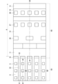
- FIG. 1 is a schematic plan view showing a schematic configuration of a semiconductor device according to Embodiment 1.
- FIG. 2 is a schematic diagram showing a schematic configuration of a boundary portion between an active region 50 and a termination region 60 in the semiconductor device according to the first embodiment.
- FIG. 3 is a schematic cross-sectional view showing a schematic configuration of a semiconductor device along line A1-A2 in FIG. 2 in Embodiment 1.
- FIG. 3 is a schematic cross-sectional view showing a schematic configuration of a semiconductor device along line B1-B2 in FIG. 2 in Embodiment 1.
- FIG. 3 is a schematic cross-sectional view showing a schematic configuration of a semiconductor device along line C1-C2 in FIG. 2 in Embodiment 1.
- FIG. 3 is a schematic cross-sectional view showing a schematic configuration of a semiconductor device taken along line D1-D2 in FIG. 2 in Embodiment 1.
- FIG. 3 is a partial cross-sectional view illustrating a method for manufacturing a semiconductor device along line B1-B2 in FIG. 2 in Embodiment 1.
- FIG. 3 is a partial cross-sectional view illustrating a method for manufacturing a semiconductor device along line B1-B2 in FIG. 2 in Embodiment 1.
- FIG. 3 is a partial cross-sectional view illustrating a method for manufacturing a semiconductor device along line B1-B2 in FIG. 2 in Embodiment 1.
- FIG. 3 is a partial cross-sectional view illustrating a method for manufacturing a semiconductor device along line B1-B2 in FIG.
- FIG. 3 is a partial cross-sectional view illustrating a method for manufacturing a semiconductor device along line B1-B2 in FIG. 2 in Embodiment 1.
- FIG. 3 is a partial cross-sectional view illustrating a method for manufacturing a semiconductor device along line B1-B2 in FIG. 2 in Embodiment 1.
- FIG. 3 is a partial cross-sectional view illustrating a method for manufacturing a semiconductor device along line D1-D2 in FIG. 2 in Embodiment 1.
- FIG. 3 is a partial cross-sectional view illustrating a method for manufacturing a semiconductor device along line D1-D2 in FIG. 2 in Embodiment 1.
- FIG. 3 is a partial cross-sectional view illustrating a method for manufacturing a semiconductor device along line D1-D2 in FIG. 2 in Embodiment 1.
- FIG. 1 is a partial cross-sectional view illustrating a method for manufacturing a semiconductor device along line D1-D2 in FIG. 2 in Embodiment 1.
- FIG. 3 is a partial cross-sectional view illustrating a method for manufacturing a semiconductor device along line D1-D2 in FIG. 2 in Embodiment 1.
- FIG. 3 is a partial cross-sectional view illustrating a method for manufacturing a semiconductor device along line D1-D2 in FIG. 2 in Embodiment 1.
- FIG. 3 is a partial cross-sectional view illustrating a method for manufacturing a semiconductor device along line D1-D2 in FIG. 2 in Embodiment 1.
- FIG. 3 is a partial cross-sectional view illustrating a method for manufacturing a semiconductor device along line D1-D2 in FIG. 2 in Embodiment 1.
- FIG. 3 is a partial cross-sectional view illustrating a method for manufacturing a semiconductor device along line D1-D2 in FIG.
- FIG. 3 is a partial cross-sectional view illustrating a method for manufacturing a semiconductor device along line D1-D2 in FIG. 2 in Embodiment 1.
- FIG. 3 is a partial cross-sectional view illustrating a method for manufacturing a semiconductor device along line D1-D2 in FIG. 2 in Embodiment 1.
- FIG. 3 is a schematic cross-sectional view showing a schematic configuration of a semiconductor device along line B1-B2 in FIG. 2 in Embodiment 2.
- FIG. 3 is a schematic cross-sectional view showing a schematic configuration of a semiconductor device taken along line C1-C2 in FIG. 2 in Embodiment 2.
- FIG. 3 is a partial cross-sectional view showing a method for manufacturing a semiconductor device along line B1-B2 in FIG. 2 in Embodiment 2.
- FIG. 3 is a partial cross-sectional view showing a method for manufacturing a semiconductor device along line B1-B2 in FIG. 2 in Embodiment 2.
- FIG. 3 is a partial cross-sectional view showing a method for manufacturing a semiconductor device along line B1-B2 in FIG. 2 in Embodiment 2.
- FIG. 3 is a partial cross-sectional view showing a method for manufacturing a semiconductor device along line B1-B2 in FIG. 2 in Embodiment 2.
- FIG. 3 is a partial cross-sectional view showing a method for manufacturing a semiconductor device along line B1-B2 in FIG.
- FIG. 3 is a partial cross-sectional view showing a method for manufacturing a semiconductor device along line B1-B2 in FIG. 2 in Embodiment 2.
- FIG. 3 is a partial cross-sectional view showing a method for manufacturing a semiconductor device along line B1-B2 in FIG. 2 in Embodiment 2.
- FIG. 3 is a partial cross-sectional view showing a method for manufacturing a semiconductor device along line C1-C2 in FIG. 2 in Embodiment 2.
- FIG. 3 is a partial cross-sectional view showing a method of manufacturing a semiconductor device along line C1-C2 in FIG. 2 in Embodiment 2.
- FIG. 3 is a partial cross-sectional view showing a method for manufacturing a semiconductor device along line C1-C2 in FIG. 2 in Embodiment 2.
- FIG. 3 is a partial cross-sectional view showing a method for manufacturing a semiconductor device along line C1-C2 in FIG. 2 in Embodiment 2.
- FIG. 3 is a partial cross-sectional view showing a method for manufacturing a semiconductor device along line C1-C2 in FIG. 2 in Embodiment 2.
- FIG. 3 is a partial cross-sectional view showing a method for manufacturing a semiconductor device along line C1-C2 in FIG. 2 in Embodiment 2.
- FIG. 3 is a partial cross-sectional view showing a method of manufacturing a semiconductor device along line C1-C2 in FIG.
- FIG. 3 is a schematic plan view showing a schematic configuration of a semiconductor device according to a third embodiment.
- FIG. 3 is a schematic diagram showing a schematic configuration of a semiconductor device according to a third embodiment.
- 40 is a schematic cross-sectional view showing a schematic configuration of a semiconductor device taken along line D1-D2 in FIG. 39 in Embodiment 3.
- FIG. FIG. 7 is a schematic diagram showing a schematic configuration of a semiconductor device according to a fourth embodiment.
- 42 is a schematic cross-sectional view showing a schematic configuration of a semiconductor device taken along line D1-D2 in FIG. 41 in Embodiment 4.
- FIG. 3 is a schematic cross-sectional view showing a schematic configuration of a semiconductor device taken along line D1-D2 in FIG. 2 in Embodiment 5.
- FIG. 40 is a schematic cross-sectional view showing a schematic configuration of a semiconductor device taken along line D1-D2 in FIG. 39 in Embodiment 5.
- FIG. 42 is a schematic cross-sectional view showing a schematic configuration of a semiconductor device along line D1-D2 in FIG. 41 in Embodiment 5.
- FIG. 42 is a schematic cross-sectional view showing a schematic configuration of a semiconductor device taken along line B1-B2 in FIG. 2, FIG. 39, or FIG. 41 in Embodiment 6.
- FIG. 40 is a schematic cross-sectional view showing a schematic configuration of a semiconductor device taken along line D1-D2 in FIG. 39 in Embodiment 5.
- FIG. 42 is a schematic cross-sectional view showing a schematic configuration of a semiconductor device taken along line B1-B2 in FIG. 2, FIG. 39
- FIG. 3 is a schematic cross-sectional view showing a schematic configuration of a semiconductor device along line D1-D2 in FIG. 2 in Embodiment 6.
- FIG. 40 is a schematic cross-sectional view showing a schematic configuration of a semiconductor device along line D1-D2 in FIG. 39 in Embodiment 6.
- FIG. 42 is a schematic cross-sectional view showing a schematic configuration of a semiconductor device along line D1-D2 in FIG. 41 in Embodiment 6.
- a component described as being provided with “one” may be provided with “one or more”. Further, a component is a conceptual unit, and one component may consist of a plurality of structures, and one component may correspond to a part of a certain structure.
- the first conductivity type of the semiconductor will be described as n-type and the second conductivity type as p-type, but conversely, the first conductivity type is assumed to be p-type and the second conductivity type is assumed to be n-type. Good too.
- a MOSFET will be described as an example of a semiconductor device, the semiconductor device may be an IGBT.
- the material of the semiconductor substrate and the drift layer will be described as silicon carbide (SiC), which is a wide bandgap semiconductor with a larger bandgap than silicon, but they may also be silicon, for example, gallium nitride, diamond, etc. Other wide bandgap semiconductors or a combination thereof may be used.
- impurity concentration indicates the peak value of impurity concentration in each region.
- FIG. 1 is a schematic plan view showing a schematic configuration of a semiconductor device according to a first embodiment.
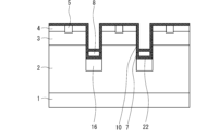
- FIG. 2 is a schematic diagram showing a schematic configuration of the boundary between the active region 50 and the termination region 60 in the semiconductor device according to the first embodiment, and shows the region 40 surrounded by the broken line in FIG. be.
- illustration of the interlayer insulating film 13, the surface electrode 14, the surface ohmic electrode 19, etc. is omitted to simplify the explanation.
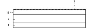
- FIGS. 3 to 6 are schematic diagrams showing cross-sectional configurations of the semiconductor device according to the first embodiment, in which FIG. 3 is a cross-sectional view taken along line A1-A2 in FIG. 2, and FIG. 5 is a sectional view taken along line C1-C2 in FIG. 2, and FIG. 6 is a sectional view taken along line D1-D2 in FIG. 2.
- the active region 50 is a region where a current flows due to the formation of a channel in the on state of the semiconductor device
- the termination region 60 is a region surrounding the active region 50.
- the termination region 60 is provided at the outer periphery of the semiconductor device chip so as to surround the active region 50, and within the termination region 60, there is a p-type termination electric field relaxation region 18 such as an FLR (Field Limiting Ring), An n-type channel stop region 31 is formed to suppress the spread of the depletion layer toward the end of the chip.
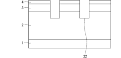
- a gate trench 22 is provided in the drift layer 2 of the active region 50, and an external trench 6 corresponding to the gate trench of the gate extension portion is provided in the drift layer 2 of the termination region 60.
- the gate trenches 22 are formed in a stripe shape when viewed from above.
- a cell is formed in each of a plurality of regions defined by gate trenches 22 in active region 50 .
- FIG. 2 shows an example in which a plurality of rectangular cells are arranged in a stripe pattern, the shape of the cells may be circular or polygonal such as a hexagonal shape, and the arrangement of the cells may be , a checkerboard pattern, a houndstooth pattern, etc. may be used.
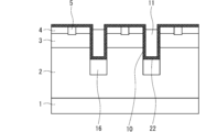
- a drift layer 2, a well region 3, an impurity region 4, a contact region 5, etc. are provided on the front side of a semiconductor substrate 1 constituting a semiconductor device.
- the active region 50 is provided with a gate trench 22, a trench bottom electric field relaxation region 16, a gate insulating film 10, and a gate electrode layer 11.
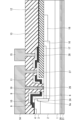
- the termination region 60 includes an external trench 6, a trench bottom electric field relaxation region 16, a trench bottom high concentration well region 17, a termination electric field relaxation region 18, an underlying insulating film 7, a potential fixing layer 8, an insulating layer 9, a gate insulating film 10, A gate electrode layer 11, a field insulating film 12, and a gate wiring electrode 15 are provided.
- Gate electrode layer 11 formed in external trench 6 of termination region 60 extends so as to surround gate trench 22 in plan view.
- a surface ohmic electrode 19 On the surface of the semiconductor substrate 1, a surface ohmic electrode 19, an interlayer insulating film 13, and a surface electrode 14 are provided in common to the active region 50 and the termination region 60.
- a back ohmic electrode 20 and a back electrode 21 are provided in common to the active region 50 and the termination region 60.
- Drift layer 2 is provided on semiconductor substrate 1 made of n-type silicon carbide, and is made of n-type silicon carbide.
- the n-type impurity of the drift layer 2 may be nitrogen or phosphorus, and the impurity concentration of the drift layer 2 may be approximately 1 ⁇ 10 14 cm ⁇ 3 or more and 1 ⁇ 10 18 cm ⁇ 3 or less.
- the thickness of the drift layer 2 may be approximately 5 ⁇ m or more and 300 ⁇ m or less.
- Well region 3 is a p-type region provided in the surface layer portion of drift layer 2, and is made of silicon carbide.
- the p-type impurity in the well region 3 may be aluminum, boron, or gallium, and the impurity concentration in the well region 3 may be approximately 1 ⁇ 10 15 cm ⁇ 3 or more and 1 ⁇ 10 20 cm ⁇ 3 or less.
- the impurity concentration of the well region 3 may or may not be constant in the depth direction.
- the thickness of the well region 3 may be about 0.3 ⁇ m or more and 3 ⁇ m or less.
- Impurity region 4 is an n-type region provided in the surface layer of well region 3, and is made of silicon carbide.
- the n-type impurity in the impurity region 4 may be nitrogen or phosphorus, and the impurity concentration in the impurity region 4 may be approximately 1 ⁇ 10 17 cm ⁇ 3 or more and 1 ⁇ 10 22 cm ⁇ 3 or less.
- the thickness of impurity region 4 may be less than or equal to the thickness of well region 3.
- Contact region 5 is provided in the surface layer of well region 3, is a p-type region having a higher impurity concentration than well region 3, and is made of silicon carbide.
- the p-type impurity in the contact region 5 may be aluminum, boron, or gallium, and the impurity concentration in the contact region 5 may be approximately 1 ⁇ 10 18 cm ⁇ 3 or more and 1 ⁇ 10 22 cm ⁇ 3 or less.
- the thickness of the contact region 5 may be equal to or less than the thickness of the well region 3.
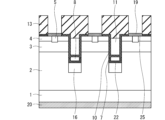
- a contact hole 25 (hereinafter referred to as “source contact hole 25") that reaches the impurity region 4 and the contact region 5 is formed in the interlayer insulating film 13, and at the bottom of the source contact hole 25, the impurity region 4 and the contact region A surface ohmic electrode 19 connected to 5 is formed.
- Impurity region 4 and contact region 5 are electrically connected to surface electrode 14 , which is a main electrode, through surface ohmic electrode 19 in source contact hole 25 .
- the contact region 5 is connected to the impurity region 4 by a surface ohmic electrode 19.
- a path is formed from the well region 3 to the surface ohmic electrode 19 via the contact region 5, and the electrical connection from the well region 3 to the surface ohmic electrode 19 is improved.
- Contact region 5 may be omitted.
- the gate trench 22 extends from the surface of the impurity region 4 through the well region 3 and reaches the drift layer 2. As shown in FIG. 2, the gate trenches 22 are provided in the active region 50 in the form of stripes (that is, in the form of a plurality of parallel lines). When the gate trenches 22 are provided in a stripe shape, when the semiconductor device is a trench gate type silicon carbide MOSFET, a surface such as a (1-100) surface with high channel mobility can be used as a channel, and the semiconductor device can improve the characteristics of Furthermore, the gate trench 22 extends in the direction of the termination region 60 . Hereinafter, the direction in which the gate trench 22 extends will be referred to as the "extending direction" of the gate trench 22.
- the width of the gate trench 22 may be, for example, approximately 0.5 ⁇ m or more and 10 ⁇ m or less.
- the width of the gate trench 22 refers to the width of the widest part of the tapered shape.
- the depth of the gate trench 22 may be, for example, approximately 0.5 ⁇ m or more and 6 ⁇ m or less.
- Trench bottom electric field relaxation region 16 is a p-type region provided below the bottom surface of gate trench 22, and is made of silicon carbide.
- the trench bottom electric field relaxation region 16 has a conductivity type opposite to that of the drift layer 2, and is designed to relieve the electric field applied to the gate insulating film 10 formed at the bottom of the gate trench 22 in the operating state of the semiconductor device. The gate insulating film 10 is thereby prevented from being destroyed.
- the depth of the trench bottom electric field relaxation region 16 may be about 0.1 ⁇ m or more and 3.0 ⁇ m or less from the bottom of the gate trench 22 downward.
- the trench bottom electric field relaxation region 16 may be in contact with the bottom surface of the gate trench 22.
- the p-type impurity of the trench bottom electric field relaxation region 16 may be aluminum, boron, or gallium, and the impurity concentration of the trench bottom electric field relaxation region 16 is 1 ⁇ 10 15 cm ⁇ 3 or more and 1 ⁇ 10 19 cm ⁇ 3 or less. It is sufficient to set it to a certain degree.
- the external trench 6 is a wide trench formed in the termination region 60 to a depth comparable to that of the gate trench 22. Also below the external trench 6, a trench bottom electric field relaxation region 16 is provided below the external trench 6.
- the trench bottom high concentration well region 17 has a conductivity type opposite to that of the drift layer 2, and is provided in the trench bottom electric field relaxation region 16 below the external trench 6.
- Trench bottom high concentration well region 17 is a p-type region with higher concentration than trench bottom electric field relaxation region 16, and is made of silicon carbide.
- a contact hole 26 (hereinafter referred to as "outer well region contact hole 26") reaching the trench bottom high concentration well region 17 is formed in the interlayer insulating film 13.
- a surface ohmic electrode 19 connected to the trench bottom high concentration well region 17 is formed.
- the trench bottom electric field relaxation region 16 is electrically connected to the surface electrode 14 through the trench bottom high concentration well region 17 and the surface ohmic electrode 19 in the outer peripheral well region contact hole 26 .
- the trench bottom high concentration well region 17 has the effect of lowering the contact resistance between the trench bottom electric field relaxation region 16 and the surface ohmic electrode 19, as well as the effect of lowering the sheet resistance of the surface of the trench bottom electric field relaxation region 16.
- the depth of the trench bottom high concentration well region 17 may be about 0.1 ⁇ m or more and 2.0 ⁇ m or less from the bottom of the external trench 6 downward.
- the trench bottom high concentration well region 17 may be in contact with the bottom of the external trench 6.
- the p-type impurity in the trench bottom high concentration well region 17 may be aluminum, boron, or gallium, and the impurity concentration in the trench bottom high concentration well region 17 is 1 ⁇ 10 18 cm ⁇ 3 or more, 1 ⁇ 10 22 cm ⁇ It may be about 3 or less.
- the termination electric field relaxation region 18 is a p-type electric field relaxation region that is formed continuously or intermittently so as to surround the active region 50, and is, for example, an FLR (Field Limiting Ring).
- the terminal electric field relaxation region 18 is formed, for example, by ion-implanting aluminum, boron, gallium, etc. from the surface of the drift layer 2 to a depth of approximately 0.2 ⁇ m to 3 ⁇ m, which does not exceed the depth of the drift layer 2.
- the p-type impurity concentration of the termination electric field relaxation region 18 is set to exceed the impurity concentration of the drift layer 2, and may be 1 ⁇ 10 15 cm ⁇ 3 or more and 1 ⁇ 10 19 cm ⁇ 3 or less.
- the field insulating film 12 is formed so as to be in contact with the surface of the drift layer 2 from inside the external trench 6 to the end of the chip.
- Field insulating film 12 can be made of an insulating material such as silicon dioxide.
- the thickness of the field insulating film 12 can be, for example, 0.1 ⁇ m or more and 5.0 ⁇ m or less.
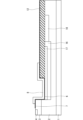
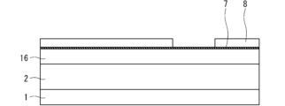
- the underlying insulating film 7 is formed to cover the inside of the external trench 6 and the upper end corner 6a of the external trench 6 (hereinafter referred to as "external trench upper end corner 6a"), and covers the well region 3, the drift layer 2, and the trench bottom electric field. It is in contact with the relaxation region 16 and the trench bottom high concentration well region 17 .
- a portion of the underlying insulating film 7 is also formed on the field insulating film 12.
- the underlying insulating film 7 is made of an insulating material such as silicon dioxide. The thickness of the underlying insulating film 7 is, for example, approximately 10 nm or more and 1000 nm or less.
- the potential fixing layer 8 is a conductive layer such as polysilicon, and is formed on the underlying insulating film 7, and covers the inside of the external trench 6 and the upper end corner 6a of the external trench via the underlying insulating film 7. A portion of potential fixing layer 8 is also formed on field insulating film 12 .
- potential fixing layer 8 is a first polysilicon layer made of polysilicon.
- a contact hole 27 (hereinafter referred to as “potential fixing layer connection contact hole 27") that reaches the potential fixing layer 8 on the field insulating film 12 is formed in the interlayer insulating film 13. It is connected to the surface electrode 14 through the contact hole 27 for layer connection. Since the potential of the surface electrode 14 becomes the source potential, the potential of the potential fixing layer 8 also becomes the source potential.
- Potential fixing layer 8 has a thickness exceeding gate insulating film 10 , preferably has a thickness exceeding three times that of gate insulating film 10 .
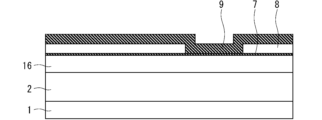
- the insulating layer 9 is formed to cover the potential fixing layer 8.
- the insulating layer 9 suppresses gate leakage current from flowing between the potential fixing layer 8 and the gate electrode layer 11.
- the insulating layer 9 is made of an insulating material such as silicon dioxide.
- the thickness of the insulating layer 9 is, for example, about 10 nm or more and 1000 nm or less, and preferably has a thickness of the gate insulating film 10 or more.
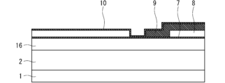
- the gate insulating film 10 is formed so as to be in contact with the inner surface of the gate trench 22, a part of the surface of the drift layer 2, the insulating layer 9, and the field insulating film 12, and is made of silicon dioxide.
- the thickness of the gate insulating film 10 can be, for example, approximately 10 nm or more and 200 nm or less.
- the gate electrode layer 11 is formed on the gate insulating film 10 in the gate trench 22 and on the gate insulating film 10 formed on the insulating layer 9 in the external trench 6. In this way, the gate insulating film 10 and the gate electrode layer 11 extend from inside the gate trench 22 to inside the external trench 6.
- the height of the upper end of the gate electrode layer 11 in the gate trench 22 is preferably lower than the surface position of the drift layer 2 , and more preferably lower than the surface position of the drift layer 2 .
- gate electrode layer 11 is a second polysilicon layer made of polysilicon.
- the gate electrode layer 11 formed in the termination region 60 has a thickness exceeding the gate insulating film 10, for example.
- a contact hole 28 (hereinafter referred to as "gate contact hole 28") that reaches the gate electrode layer 11 is formed in the interlayer insulating film 13, and the gate electrode layer 11 connects to the gate electrode pad 29 through the gate contact hole 28. It is connected to the gate wiring electrode 15 connected to.
- the surface electrode 14, gate wiring electrode 15, and gate electrode pad 29 are formed on the interlayer insulating film 13, and are made of a metal material such as aluminum.
- the surface electrode 14, the gate wiring electrode 15, and the gate electrode pad 29 are arranged apart from each other.
- the back ohmic electrode 20 is formed on the back surface of the semiconductor substrate 1 and is made of a reaction product of the semiconductor substrate 1 and a metal film containing nickel as a main component, such as nickel silicide.
- the back electrode 21 is formed in contact with the back ohmic electrode 20 and is made of titanium, nickel, silver, gold, aluminum, or the like.
- the semiconductor device according to Embodiment 1 is composed of the above components.
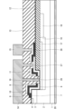
- FIGS. 7 to 21 are explanatory diagrams of each manufacturing stage of a semiconductor device, of which FIGS. 7 to 12 correspond to the cross section taken along the line B1-B2 in FIG. 2, and FIGS. This corresponds to the cross section along the D1-D2 line of No. 2.
- an n-type silicon carbide semiconductor substrate 1 having a 4H polytype is prepared, and an n-type drift layer 2 is epitaxially grown thereon by chemical vapor deposition (CVD).
- the impurity concentration of the n-type drift layer 2 is in the range of 1 ⁇ 10 14 cm ⁇ 3 to 1 ⁇ 10 18 cm ⁇ 3 , and the thickness of the drift layer 2 is 5 ⁇ m to 300 ⁇ m.
- a p-type well region 3 is formed in the surface layer of the drift layer 2 by ion-implanting aluminum, boron, or gallium using a resist mask formed on the drift layer 2 by photolithography.
- Well region 3 may be formed by epitaxial growth.
- nitrogen or phosphorus ions are implanted to form an n-type impurity region 4 in the surface layer of the well region 3.
- a silicon dioxide film with a thickness of about 1 ⁇ m to 2 ⁇ m is formed on the well region 3 and impurity region 4, and the formation regions of the gate trench 22 and external trench 6 are etched by reactive ion etching (RIE). An open etching mask is formed. Then, when the gate trench 22 and the external trench 6 are formed by RIE, the states shown in FIGS. 7 and 13 are obtained.
- RIE reactive ion etching
- a resist mask covering a part of the external trench 6 is formed by photolithography, and then aluminum, boron, or gallium is ion-implanted from the surface side of the drift layer 2 to form a gate.
- a trench bottom electric field relaxation region 16 is formed below the trench 22 and the external trench 6.
- ions of aluminum, boron, or gallium are implanted from the surface side of the drift layer 2 to form a termination in the termination region 60.
- An electric field relaxation region 18 is formed.
- the heating temperature of the semiconductor substrate 1 during this ion implantation is preferably 150° C. or higher. When the heating temperature is 150° C. or higher, the electrical resistance of the contact region 5 can be lowered, and resistance loss during the operating state of the semiconductor device can be reduced.
- an annealing process is performed to activate the ion-implanted impurities.
- the annealing treatment is performed in an inert gas atmosphere such as argon or in vacuum at a temperature of approximately 1500° C. or higher and 1900° C. or lower for approximately 30 seconds or more and 1 hour or less.
- a carbon film may be formed on semiconductor substrate 1 before the annealing treatment. In this way, the states shown in FIGS. 8 and 14 are achieved.
- an insulating film such as silicon dioxide, which will become the field insulating film 12, is formed by CVD or the like, and a resist mask is formed on this insulating film by photolithography. Then, this insulating film is opened by etching to form a field insulating film 12, and the resist mask is removed. In this way, the state shown in FIG. 15 is reached.
- the inside and upper end corners of the external trench 6 are covered by a thermal oxidation method or a CVD method, and an underlay is applied so as to be in contact with the well region 3, the drift layer 2, the trench bottom electric field relaxation region 16, and the trench bottom high concentration well region 17.
- An insulating film 7 is formed. A portion of the underlying insulating film 7 is also formed on the field insulating film 12.
- a conductive material such as polysilicon that will become the potential fixing layer 8 is formed on the underlying insulating film 7 by CVD or the like, and a resist mask is formed on the polysilicon by photolithography.
- the potential fixing layer 8 is formed in the termination region 60 by etching the polysilicon.
- a portion of potential fixing layer 8 is also formed on field insulating film 12 .
- all of the polysilicon in the active region 50 is removed by etching until the underlying insulating film 7 is exposed by an etch-back process. After that, the resist mask is removed. In this way, the state shown in FIG. 16 is achieved.
- a layer of silicon dioxide or the like, which will become the insulating layer 9, is formed to cover the potential fixing layer 8 by a CVD method or the like.
- potential fixing layer 8 is made of polysilicon
- this layer of silicon dioxide or the like may be formed by thermally oxidizing the surface of potential fixing layer 8.
- a resist mask is formed by photolithography, and the insulating layer 9 is formed by etching.
- the underlying insulating film 7 and insulating layer 9 in the gate trench 22 in the active region 50 are completely removed by etching to expose the drift layer 2. In this way, the state shown in FIG. 17 is achieved.
- a gate insulating film 10 is formed on the surface of the drift layer 2, the inner surface of the gate trench 22, and the insulating layer 9 and field insulating film 12 in the termination region 60 by a thermal oxidation method, a CVD method, or the like. In this way, the states shown in FIGS. 9 and 18 are achieved.
- a conductive material such as polysilicon that will become the gate electrode layer 11 is formed by CVD or the like, and a resist mask is formed on the polysilicon by photolithography.
- the gate electrode layer 11 is formed by etching the polysilicon, and the resist mask is removed.
- the polysilicon in the active region 50 is etched by an etch-back process so that the upper end of the gate electrode layer 11 is below the surface position of the drift layer 2 in the gate trench 22. In this way, the states shown in FIGS. 10 and 19 are achieved.
- an interlayer insulating film 13 is formed by low pressure CVD or the like, and a resist mask is formed on the interlayer insulating film 13 by photolithography. Subsequently, by etching the interlayer insulating film 13, a source contact hole 25 reaching the impurity region 4 and the contact region 5, and an outer peripheral well region contact hole 26 reaching the trench bottom high concentration well region 17 are formed.
- a metal containing Ni or the like as a main component is applied over the impurity region 4 and contact region 5 exposed to the source contact hole 25 and over the trench bottom high concentration well region 17 exposed to the outer peripheral well region contact hole 26.
- a film is formed and annealing is performed to form a surface ohmic electrode 19.
- the metal film on the interlayer insulating film 13 is removed by etching, and the resist mask is removed.
- a metal film containing Ni or the like as a main component is formed on the back surface of the semiconductor substrate 1, and annealing treatment is performed to form the back ohmic electrode 20.
- the heating temperature of each annealing treatment may be approximately 600° C. or higher and 1100° C. or lower.
- a resist mask is formed on the interlayer insulating film 13 by photolithography, and the interlayer insulating film 13 is etched to form a potential fixing layer connection contact hole 27 that reaches the potential fixing layer 8 and a gate electrode layer 11.
- a gate contact hole 28 is formed to reach the surface, and the resist mask is removed. In this way, the states shown in FIGS. 11 and 20 are achieved.
- a metal film such as aluminum is formed on the interlayer insulating film 13 and the surface ohmic electrode 19 and inside the potential fixing layer connection contact hole 27 and the gate contact hole 28 by sputtering or vapor deposition.
- a resist mask is formed thereon by photolithography.
- the metal film is patterned by etching to form the surface electrode 14, the gate wiring electrode 15, and the gate electrode pad 29, and then the resist mask is removed. In this way, the states shown in FIGS. 12 and 21 are achieved.
- the structure of the semiconductor device shown in FIGS. 4 and 6 is completed by forming the back electrode 21 on the back ohmic electrode 20 by sputtering, vapor deposition, or the like.
- the termination region 60 may be provided with a channel stop region 31 that suppresses the expansion of the depletion layer toward the end of the semiconductor device.
- Channel stop region 31 is an n-type region provided on the outer peripheral side of external trench 6, and is made of silicon carbide.
- the n-type impurity of the channel stop region 31 may be nitrogen or phosphorus, and the impurity concentration of the channel stop region 31 may be approximately 1 ⁇ 10 17 cm ⁇ 3 or more and 1 ⁇ 10 22 cm ⁇ 3 or less.
- the thickness of channel stop region 31 may be the same as the thickness of impurity region 4, or may be different.
- the channel stop region 31 may be formed by ion implantation, and may be formed simultaneously with the impurity region 4 using a resist mask for providing the impurity region 4, or may be formed before or after the formation of the impurity region 4. You may. When forming channel stop region 31 and impurity region 4 at the same time, channel stop region 31 and impurity region 4 may be formed, for example, after gate trench 22 and external trench 6 are formed.
- the well region 3 and the impurity region 4 are formed by ion-implanting n-type impurities into the surface layer of the well region 3 to form the impurity region 4, and then forming a resist mask by photolithography on it to form the impurity region 4.
- the well region 3 may be formed by ion-implanting p-type impurities to a position other than the region 4.
- the thickness of the etching mask and the RIE process are adjusted so that the etching mask remains after forming the gate trench 22 and the external trench 6, and the remaining etching mask and the photolithography process are used to form the etching mask.
- a trench bottom electric field relaxation region 16 was formed by ion implantation using a resist mask.
- the trench bottom electric field relaxation region 16 may be formed by ion implantation using only a resist mask formed by photolithography and removing the etching mask without leaving it.
- the trench bottom electric field relaxation region 16 below the external trench 6 may be formed at the same time as the trench bottom electric field relaxation region 16 under the gate trench 22, or before the formation of the trench bottom electric field relaxation region 16 under the gate trench 22. Alternatively, it may be formed later. Furthermore, p-type impurity ions are implanted obliquely into the gate trench 22 to form a p-type semiconductor layer in the drift layer 2 in contact with the side surfaces of the gate trench 22, forming the trench bottom electric field relaxation region 16 and the well region. 3 may be electrically connected to each other through the semiconductor layer.
- the trench bottom electric field relaxation region 16 and the well region 3 are electrically connected, the trench bottom electric field relaxation region 16 is connected to the surface electrode 14 via the well region 3, compared to the state where the trench bottom electric field relaxation region 16 is floating. Since it is grounded and grounded, the frequency characteristics of the semiconductor device are improved.
- the semiconductor device is a MOSFET, but when the semiconductor device is an IGBT, the conductivity type of the semiconductor substrate 1 may be p-type, and the semiconductor substrate 1 may be polished to have a thickness of You can make it thinner.
- the gate insulating film 10 when the gate insulating film 10 is formed in contact with the surfaces and inside of the gate trench 22 and the external trench 6, the upper end corner 22a of the external trench 6 (hereinafter referred to as "gate trench upper end corner 22a") and An electric field is generated in the gate insulating film 10 near the upper end corner 6a of the external trench.
- the gate electrode layer 11 is formed at a position lower than the gate trench top corner 22a, so that electric field concentration due to the shape of the gate trench top corner 22a is suppressed, and the gate insulating film 11 is destruction is prevented.
- the gate insulating film 10 is formed on the insulating layer 9 and is spaced apart from the top corner 6a of the external trench, so that electric field concentration due to the shape of the top corner 6a of the external trench occurs. This prevents the gate insulating film 10 from being destroyed.
- the upper end corner 6a of the external trench is covered with an underlying insulating film 7, and the well region 3 and the potential fixing layer 8 are at the source potential, and the potential fixing layer 8 is connected to the gate electrode by the insulating layer 9 and the gate insulating film 10. Since it is insulated from the layer 11, the underlying insulating film 7 at the upper end corner 6a of the external trench is not destroyed by the gate voltage.
- the potential fixing layer 8 covers the upper end corner and the inside of the external trench 6 via the underlying insulating film 7.
- the curvature of the upper part can be increased.
- the thickness of the insulating layer 9 when the thickness of the insulating layer 9 is thin, the insulation between the potential fixing layer 8 and the gate electrode layer 11 becomes insufficient, and as in the case where the potential of the field plate electrode is set as the source potential in Patent Document 2, there is a difference between the gate and the source. Leakage increases, and the potential fixing layer 8 and gate electrode layer 11 may be destroyed by the electric field, resulting in a short circuit. In order to avoid this, it is preferable that the thickness of the insulating layer 9 be greater than the thickness of the gate insulating film 10, for example.
- the depletion layer also spreads from the trench bottom electric field relaxation region 16 to the drift layer 2. This suppresses breakdown of the gate insulating film 10 at the bottoms or bottom corners of the gate trenches 22 and external trenches 6 due to the electric field generated by the high voltage applied between the front electrode 14 and the back electrode 21 .
- the semiconductor device shifts from the off state to the on state, the voltage applied between the front electrode 14 and the back electrode 21 decreases, and the depletion layer that had spread to the drift layer 2 contracts.
- the semiconductor device operates so as to alternately repeat the above-described on state and off state.
- the semiconductor device According to the semiconductor device according to the first embodiment, it is possible to prevent the gate insulating film 10 from being destroyed at the gate trench top corner 22a and the external trench top corner 6a.
- FIG. 22 and 23 are diagrams showing the configuration of a semiconductor device according to the second embodiment, in which FIG. 22 is a cross-sectional view taken along line B1-B2 in FIG. 2, and FIG. 23 is a cross-sectional view taken along line C1-C2 in FIG. Each corresponds to a cross-sectional view along the line.
- the cross-sectional configuration along lines A1-A2 and D1-D2 in FIG. 2 is the same as that in the first embodiment.
- an underlying insulating film 7 and a potential fixing layer 8 are provided below the gate insulating film 10 and the gate electrode layer 11 in the gate trench 22 of the active region 50.
- the underlying insulating film 7 is formed in contact with the inner surface of the gate trench 22, and the potential fixing layer 8 is formed on the underlying insulating film 7.
- the gate insulating film 10 is formed in contact with the inner surface of the gate trench 22 and the upper surface of the potential fixing layer 8 , and the gate electrode layer 11 is formed on the gate insulating film 10 .
- the potential of the potential fixing layer 8 formed in the gate trench is a floating potential.
- the underlying insulating film 7 is formed thicker than the gate insulating film 10 in order to alleviate the influence of the electric field generated on the bottom surface of the gate trench 22 due to the drain voltage.
- the trench bottom electric field relaxation region 16 is formed below the gate trench 22, but the trench bottom electric field relaxation region 16 may be omitted.
- the electric field generated at the bottom of the gate trench 22 by the drain voltage when the semiconductor device is off is caused by the depletion layer formed between the well region 3 and the drift layer 2 and the underlying insulation. It is shared between the membrane 7 and the potential fixing layer 8.
- concentration of phosphorus in the polysilicon of the potential fixing layer 8 is lowered, depletion of the polysilicon increases and the electric field relaxation effect can be enhanced.
- the semiconductor device caused by the depletion layer extending from the well region 3 to the drift layer 2 and the depletion layer extending from the trench bottom electric field relaxation region 16 to the drift layer 2 is Since the current confinement is eliminated, it is also possible to improve the on-state characteristics.
- FIGS. 24 to 37 are explanatory diagrams of each manufacturing stage of a semiconductor device, of which FIGS. 24 to 30 correspond to the cross section taken along the line B1-B2 in FIG. This corresponds to a cross section taken along the C1-C2 line.
- an n-type silicon carbide semiconductor substrate 1 having a 4H polytype is prepared, and an n-type drift layer 2 is deposited thereon by chemical vapor deposition (CVD). is epitaxially grown to form a well region 3, an impurity region 4, a gate trench 22, and a trench bottom electric field relaxation region 16. In this way, the states shown in FIGS. 24 and 31 are achieved.
- CVD chemical vapor deposition
- an insulating film such as silicon dioxide, which will become the field insulating film 12, is formed by CVD or the like, and a resist mask is formed on this insulating film by photolithography. Then, this insulating film is opened by etching to form a field insulating film 12, and the resist mask is removed.
- the underlying insulating film 7 is formed by a thermal oxidation method, a CVD method, or the like. In this way, the states shown in FIGS. 25 and 32 are achieved.
- a conductive material such as polysilicon that will become the potential fixing layer 8 is formed on the underlying insulating film 7 by CVD or the like, and is etched by an etch-back process so that a desired thickness remains in the gate trench 22.
- a resist mask is formed by photolithography, and the potential fixing layer 8 in the active region 50 and the potential fixing layer 8 in the termination region 60 are etched so that the potential fixing layer 8 in the active region 50 has a floating potential. Separate and remove the resist mask. In this way, the states shown in FIGS. 26 and 33 are achieved.
- an insulating layer 9 made of silicon dioxide or the like is formed to cover the potential fixing layer 8 by a CVD method or the like.
- the insulating layer 9 may be formed by thermally oxidizing the potential fixing layer 8. In this way, the states shown in FIGS. 27 and 34 are achieved.
- a resist mask is formed by photolithography, and etching is performed until the upper side and the upper end of the sidewall of the potential fixing layer 8 in the gate trench 22 are exposed.
- a gate insulating film 10 is formed on the surface of the drift layer 2, inside the gate trench 22, and on the insulating layer 9 by a thermal oxidation method, a CVD method, or the like. In this way, the states shown in FIGS. 28 and 35 are achieved.
- a conductive material such as polysilicon that will become the gate electrode layer 11 is formed by CVD or the like, and a resist mask is formed on the polysilicon by photolithography.
- the gate electrode layer 11 is formed by etching the polysilicon, and the resist mask is removed.
- the polysilicon in the active region 50 is etched by an etch-back process so that the upper end of the gate electrode layer 11 is below the surface position of the drift layer 2 in the gate trench 22. In this way, the states shown in FIGS. 29 and 36 are achieved.
- an interlayer insulating film 13 is formed by low pressure CVD or the like, and a resist mask is formed on the interlayer insulating film 13 by photolithography. Subsequently, by etching the interlayer insulating film 13, a source contact hole 25 reaching the impurity region 4 and the contact region 5, and an outer peripheral well region contact hole 26 reaching the trench bottom high concentration well region 17 are formed.
- a metal containing Ni or the like as a main component is applied over the impurity region 4 and contact region 5 exposed to the source contact hole 25 and over the trench bottom high concentration well region 17 exposed to the outer peripheral well region contact hole 26.
- a film is formed and annealing is performed to form a surface ohmic electrode 19.
- the metal film on the interlayer insulating film 13 is removed by etching, and the resist mask is removed.
- a metal film containing Ni or the like as a main component is formed on the back surface of the semiconductor substrate 1, and annealing treatment is performed to form the back ohmic electrode 20.
- the heating temperature of each annealing treatment may be approximately 600° C. or higher and 1100° C. or lower. In this way, the states shown in FIGS. 30 and 37 are achieved.
- a metal film such as aluminum is formed on the interlayer insulating film 13 and the surface ohmic electrode 19 and inside the potential fixing layer connection contact hole 27 and the gate contact hole 28 by sputtering or vapor deposition.
- a resist mask is formed thereon by photolithography.
- the metal film is patterned by etching to form the surface electrode 14, the gate wiring electrode 15, and the gate electrode pad 29, and then the resist mask is removed.
- the structure of the semiconductor device shown in FIGS. 22 and 23 is completed by forming the back electrode 21 on the back ohmic electrode 20 by sputtering, vapor deposition, or the like.
- the potential fixing layer 8 of the active region 50 and the potential fixing layer 8 of the termination region 60 are separated by etching so that the potential fixing layer 8 in the active region 50 has a floating potential.
- the potential fixing layer 8 of the termination region 60 is set to a floating potential without being connected to an external electrode, the potential fixation layer 8 of the active region 50 and the potential fixing layer 8 of the termination region 60 are fixed.
- the layers 8 may be connected to each other.
- the semiconductor device according to the second embodiment also provides the same effects as the first embodiment. Further, the thickness of the underlying insulating film 7 formed on the bottom surface of the gate trench 22 is thicker than the gate insulating film 10, so that the gate electrode layer 11 is not located on the bottom surface of the gate trench 22. Therefore, compared to the case where only the gate insulating film 10 is formed on the bottom surface of the gate trench 22, the insulating film (such as silicon dioxide) on the bottom surface of the gate trench 22 is The effect of the generated electric field is alleviated.
- FIG. 38 to 40 are diagrams showing the configuration of a semiconductor device according to the third embodiment.
- FIG. 38 is a schematic plan view showing the general structure of the semiconductor device according to the third embodiment
- FIG. 39 shows the structure of the region 41 surrounded by the broken line in FIG. 38.
- FIG. 40 is a cross-sectional view taken along line D1-D2 in FIG. 39.
- illustrations of the interlayer insulating film 13, the surface electrode 14, the surface ohmic electrode 19, etc. are omitted to simplify the explanation.
- the semiconductor device includes a ground electrode pad 30 to which a ground potential of 0V is supplied and a ground wiring electrode 23 connected thereto.
- the potential fixing layer 8 is connected to the surface electrode 14, and the potential of the potential fixing layer 8 is used as the source potential.
- the potential fixing layer 8 is connected to the ground wiring electrode 23, and the potential of the potential fixing layer 8 is set to the ground potential.
- the configuration other than this is the same as that of the first embodiment.
- the gate insulating film 10 is formed separated from the top corner 6a of the external trench, so that the electric field due to the shape of the top corner 6a of the external trench is Concentration is suppressed and destruction of the gate insulating film 10 is prevented.
- the upper end corner 6a of the external trench is covered with an underlying insulating film 7, the well region 3 is at a source potential, the potential fixing layer 8 is at a ground potential, and the potential fixing layer 8 is connected to an insulating layer 9 and a gate insulating film 10. Since the underlying insulating film 7 at the upper corner portion 6a of the external trench is insulated from the gate electrode layer 11 by the gate voltage, the underlying insulating film 7 is not destroyed by the gate voltage.
- FIG. 41 and 42 are diagrams showing the configuration of a semiconductor device according to the fourth embodiment.
- FIG. 41 is a schematic diagram showing a schematic configuration of a semiconductor device according to Embodiment 4, and shows the configuration of a region 40 surrounded by a broken line in FIG. 1.
- FIG. 42 is a cross-sectional view taken along line D1-D2 in FIG. 41.
- illustration of the interlayer insulating film 13, the surface electrode 14, the surface ohmic electrode 19, etc. is omitted to simplify the explanation.
- the potential fixing layer connection contact hole 27 is not formed in the interlayer insulating film 13, and the potential fixing layer 8 is not connected to any other electrode.
- the potential of the potential fixing layer 8 is set to a floating potential.
- the configuration other than this is the same as in the first to third embodiments.
- the gate insulating film 10 is formed in the termination region 60 so as to be separated from the top corner 6a of the external trench, so that the electric field caused by the shape of the top corner 6a of the external trench is Concentration is suppressed and destruction of the gate insulating film 10 is prevented.
- the upper end corner 6a of the external trench is covered with an underlying insulating film 7, but the well region 3 is at a source potential, the potential fixing layer 8 is at a floating potential, and the potential fixing layer 8 is connected to the insulating layer 9 and the gate insulating film 10. Since the underlying insulating film 7 at the upper corner portion 6a of the external trench is insulated from the gate electrode layer 11 by the gate voltage, the underlying insulating film 7 is not destroyed by the gate voltage.
- FIG. 43 to 45 are diagrams showing the configuration of a semiconductor device according to the fifth embodiment.
- 43 is a sectional view taken along line D1-D2 in FIG. 2
- FIG. 44 is a sectional view taken along line D1-D2 in FIG. 39
- FIG. 45 is a sectional view taken along line D1-D2 in FIG.
- the well region 3 and the trench bottom electric field relaxation region 16 were separated from each other in the termination region 60.
- the well region 3 and the trench bottom electric field relaxation region 16 are connected to each other by a p-type external trench side surface connection layer 24 formed on the side surface of the external trench 6.
- the configuration other than this is the same as in the first to fourth embodiments.
- 43 shows the configuration of FIG. 6 with an external trench side connection layer 24 provided
- FIG. 44 shows the configuration of FIG. 40 with an external trench side connection layer 24 provided
- FIG. 45 shows the configuration of FIG. 42. This corresponds to a structure in which an external trench side surface connection layer 24 is provided.
- the external trench side surface connection layer 24 is formed, for example, by ion implantation after the formation of the trench bottom electric field relaxation region 16, and the p-type impurity may be aluminum, boron, or gallium, and the impurity concentration is 1 ⁇ 10 17 cm ⁇ 3 or more. , about 1 ⁇ 10 22 cm ⁇ 3 or less.
- 46 to 49 are diagrams showing the configuration of a semiconductor device according to the fifth embodiment.
- 46 is a cross-sectional view taken along line B1-B2 in FIG. 2, FIG. 39 or FIG. 41
- FIG. 47 is a cross-sectional view taken along line D1-D2 in FIG.
- FIG. 49 is a cross-sectional view taken along line D1-D2 in FIG. 41.
- the underlying insulating film 7 is not formed, and the potential fixing layer 8 is in contact with the inner surface of the external trench 6 and the upper end corner 6a of the external trench.
- the configuration other than this is the same as in the first to fifth embodiments.
- 47 shows the structure of FIG. 43 with the underlying insulating film 7 omitted
- FIG. 48 shows the structure of FIG. 44 with the underlying insulating film 7 omitted
- FIG. 49 shows the structure of FIG. 45 with the underlying insulating film 7 removed. This corresponds to omitting 7.
- the gate insulating film 10 is formed in the termination region 60 so as to be separated from the top corner 6a of the external trench, so that electric field concentration due to the shape of the top corner 6a of the external trench is prevented. This suppresses the damage and prevents the gate insulating film 10 from being destroyed.
- the potential of the potential fixing layer 8 is set to one of the source potential, ground potential, and floating potential. Even if the potential of the potential fixing layer 8 is the source potential or the ground potential, the drift layer 2 can be Due to the influence of the PN junction, it is difficult for current to flow from the back electrode 21 to the potential fixing layer 8, and the influence on loss is small.
Abstract
A semiconductor device comprises a gate trench (22) formed in an active region (50); a gate insulating film (10) and a gate electrode layer (11) formed inside the gate trench (22); a gate wiring electrode (15) formed on an interlayer insulating film (13) that covers the gate electrode layer (11); and an external trench (6) formed in a drift layer (2) in an end region (60). A potential fixing layer (8) that covers an upper end corner section (6a) of the external trench (6), and an insulating layer (9) formed on the potential fixing layer (8), are formed inside the external trench (6). The gate insulating film (10) and the gate electrode layer (11) extend into the external trench (6), and the gate electrode layer (11) is connected to the gate wiring electrode (15) via a contact hole formed in the interlayer insulating film (13) inside the external trench (6).
Description
本開示は、トレンチゲート型の半導体装置およびその製造方法に関し、特に半導体装置の外周側のゲート電極の構造に関する。
The present disclosure relates to a trench gate type semiconductor device and a method for manufacturing the same, and particularly relates to a structure of a gate electrode on the outer peripheral side of the semiconductor device.
車載機器、産業機器等の電力制御用途において、トレンチゲート構造を有する、絶縁ゲート型バイポーラトランジスタ(IGBT:Insulated Gate Bipolar Transistor)、絶縁ゲート型電界効果トランジスタ(MOSFET:Metal Oxide Semiconductor Field Effect Transistor)等の半導体装置が用いられている。
Insulated gate bipolar transistors (IGBTs), insulated gate field effect transistors (MOSFETs), etc. with trench gate structures are used for power control applications in automotive equipment, industrial equipment, etc. Semiconductor devices are used.
トレンチゲート構造を有する半導体装置には、ゲート電極が埋め込まれたトレンチ(以下「ゲートトレンチ」という)を主電流が流れる活性領域からその外側の終端領域まで延伸させた「ゲート引き出し部」が設けられる。半導体装置がオンした状態ではドレイン電圧は低いものの、ゲート電極に電圧が印加されるため、ゲート絶縁膜に生じる電界が高くなり、特にゲートトレンチの上端角部に電界が集中しやすい。
A semiconductor device having a trench gate structure is provided with a "gate extension section" in which a trench in which a gate electrode is embedded (hereinafter referred to as "gate trench") extends from an active region through which a main current flows to a termination region outside the active region. . Although the drain voltage is low when the semiconductor device is on, a voltage is applied to the gate electrode, so the electric field generated in the gate insulating film increases, and the electric field tends to concentrate particularly at the upper corner of the gate trench.
下記の特許文献1には、ゲート引き出し部のゲートトレンチにおいて、LOCOS(Local Oxidation of Silicon)酸化で形成した厚いフィールド絶縁膜に接するようにゲート絶縁膜を形成することで、当該ゲートトレンチ上端角部の電界集中を低減させる技術が開示されている。
Patent Document 1 below discloses that by forming a gate insulating film in contact with a thick field insulating film formed by LOCOS (Local Oxidation of Silicon) oxidation in a gate trench of a gate extension part, the upper corner of the gate trench is A technique for reducing electric field concentration has been disclosed.
また、下記の特許文献2には、ゲート引き出し部のゲートトレンチ内にゲート電極とともにフィールドプレート電極を設け、フィールドプレート電極の電位をゲート電位もしくはソース電位とする技術が開示されている。
Further, Patent Document 2 below discloses a technique in which a field plate electrode is provided together with a gate electrode in a gate trench of a gate extension portion, and the potential of the field plate electrode is set to the gate potential or the source potential.
特許文献1のようにフィールド絶縁膜によってゲート引き出し部のゲート絶縁膜の耐圧向上を図ったとしても、例えばゲートトレンチの上端角部が直角形状から外れる庇状の部分を有する場合には、局所的にフィールド絶縁膜の薄い箇所が形成されるため、ゲート絶縁膜の耐圧向上の効果が十分に得られない。
Even if the field insulating film is used to improve the withstand voltage of the gate insulating film in the gate lead-out portion as in Patent Document 1, for example, if the upper end corner of the gate trench has an eave-like part that deviates from a right-angled shape, local Since a thin portion of the field insulating film is formed in the gate insulating film, the effect of improving the withstand voltage of the gate insulating film cannot be sufficiently obtained.
特許文献2に開示されたゲート引き出し部において、フィールドプレート電極の電位をゲート電位とした場合は、ゲート絶縁膜の厚みが十分厚くなければゲートトレンチの上端角部でゲート絶縁膜の破壊が生じるおそれがある。一方、フィールドプレート電極の電位をソース電位とした場合は、ゲート電極とフィールドプレート電極との間の絶縁膜を通してゲート・ソース間リーク電流が発生するおそれがある。また、フィールドプレート電極の形状によっては、フィールドプレート電極上に形成されるゲート絶縁膜の薄い箇所が局所的に形成されて、ゲート絶縁膜の破壊を招くおそれもある。
In the gate lead-out portion disclosed in Patent Document 2, when the potential of the field plate electrode is set to the gate potential, if the thickness of the gate insulating film is not sufficiently thick, there is a risk that the gate insulating film will be destroyed at the upper corner of the gate trench. There is. On the other hand, if the potential of the field plate electrode is set to the source potential, there is a risk that a leak current between the gate and the source may occur through the insulating film between the gate electrode and the field plate electrode. Further, depending on the shape of the field plate electrode, thin portions of the gate insulating film formed on the field plate electrode may be locally formed, leading to destruction of the gate insulating film.
本開示は以上のような課題を解決するためになされたものであり、ゲート引き出し部のゲートトレンチの上端角部におけるゲート絶縁膜の破壊を防止できる半導体装置を提供することを目的とする。
The present disclosure has been made to solve the above-mentioned problems, and it is an object of the present disclosure to provide a semiconductor device that can prevent breakdown of the gate insulating film at the upper end corner of the gate trench of the gate extension portion.
本開示に係る半導体装置は、第1導電型のドリフト層と、前記ドリフト層の表層部に形成された第2導電型のウェル領域と、前記ウェル領域の表層部に形成された第1導電型の不純物領域と、活性領域の前記不純物領域および前記ウェル領域を貫通して前記ドリフト層に達するように形成されたゲートトレンチと、前記ゲートトレンチの内面に接して形成されたゲート絶縁膜と、前記ゲート絶縁膜上に形成されたゲート電極層と、前記ゲート電極層を覆う層間絶縁膜と、前記層間絶縁膜上に形成され、前記ゲート電極層と接続されたゲート配線電極と、前記活性領域の外側の終端領域において前記ドリフト層に形成された外部トレンチと、前記外部トレンチ内に形成され、前記外部トレンチの上端角部を覆う電位固定層と、前記電位固定層の上に形成された絶縁層と、を備え、前記ゲート絶縁膜および前記ゲート電極層は、前記終端領域の前記外部トレンチ内にまで延在し、前記ゲート電極層は、前記外部トレンチ内で前記層間絶縁膜に形成されたコンタクトホールを通して前記ゲート配線電極と接続する。
A semiconductor device according to the present disclosure includes a drift layer of a first conductivity type, a well region of a second conductivity type formed in a surface layer portion of the drift layer, and a well region of a first conductivity type formed in a surface layer portion of the well region. a gate trench formed to penetrate the impurity region and the well region of the active region and reach the drift layer; a gate insulating film formed in contact with the inner surface of the gate trench; a gate electrode layer formed on a gate insulating film; an interlayer insulating film covering the gate electrode layer; a gate wiring electrode formed on the interlayer insulating film and connected to the gate electrode layer; an external trench formed in the drift layer in the outer termination region; a potential fixing layer formed in the external trench and covering the upper corner of the external trench; and an insulating layer formed on the potential fixing layer. and, the gate insulating film and the gate electrode layer extend into the external trench of the termination region, and the gate electrode layer is connected to a contact formed on the interlayer insulating film within the external trench. It is connected to the gate wiring electrode through the hole.
本開示によれば、外部トレンチの上端角部が電位固定層および絶縁層で覆われているため、外部トレンチに引き出されたゲート電極およびゲート絶縁膜は絶縁層上に形成され、外部トレンチの上端角部から離隔される。そのため、外部トレンチの上端角部の形状に起因する電界集中によってゲート絶縁膜が破壊されることが防止される。
According to the present disclosure, since the upper end corner of the external trench is covered with the potential fixing layer and the insulating layer, the gate electrode and gate insulating film drawn out to the external trench are formed on the insulating layer, and the upper end corner of the external trench is covered with the potential fixing layer and the insulating layer. separated from the corner. Therefore, the gate insulating film is prevented from being destroyed due to electric field concentration caused by the shape of the upper corner of the external trench.
本開示の目的、特徴、態様、および利点は、以下の詳細な説明と添付図面とによって、より明白となる。
Objects, features, aspects, and advantages of the present disclosure will become more apparent from the following detailed description and accompanying drawings.
以下、本開示に係る技術の実施の形態について図面を参照しながら説明する。図面は模式的に示されたものであり、異なる図面にそれぞれ示されている画像のサイズおよび位置の相互関係は、必ずしも正確に記載されたものではなく、適宜変更され得る。また、同様の構成要素には同じ符号を付して図示し、それらの名称および機能も同様のものとする。よって、それらについての詳細な説明を省略する場合がある。
Hereinafter, embodiments of the technology according to the present disclosure will be described with reference to the drawings. The drawings are shown schematically, and the mutual relationship between the sizes and positions of the images shown in different drawings is not necessarily exactly described and may be changed as appropriate. Further, similar components are shown with the same reference numerals, and their names and functions are also the same. Therefore, detailed explanations thereof may be omitted.
説明において、「上」、「下」、「側」、「底」、「表」又は「裏」などの特定の位置および方向を意味する用語が用いられることがあるが、これらの用語は、実施の形態の理解を容易にするため便宜上用いられており、実使用時の位置および方向とは関係しない。
In the description, terms such as "top," "bottom," "side," "bottom," "front," or "back" that mean specific positions and directions are sometimes used; It is used for convenience to facilitate understanding of the embodiment, and is not related to the position and direction in actual use.
矛盾が生じない限り、「1つ」備えられるものとして記載された構成要素は、「1つ以上」備えられていてもよい。また、構成要素は概念的な単位であって、1つの構成要素が複数の構造物から成る場合、および1つの構成要素がある構造物の一部に対応することもある。
Unless a contradiction occurs, a component described as being provided with "one" may be provided with "one or more". Further, a component is a conceptual unit, and one component may consist of a plurality of structures, and one component may correspond to a part of a certain structure.
以下の実施の形態では、半導体の第1導電型をn型、第2導電型をp型として説明するが、それとは逆に、第1導電型をp型、第2導電型はn型としてもよい。また、半導体装置の例としてMOSFETを説明するが、半導体装置はIGBTであってもよい。また、半導体基板およびドリフト層の材料は、シリコンよりもバンドギャップが大きいワイドバンドギャップ半導体である炭化珪素(SiC)であるものとして説明するが、それらはシリコンでもよいし、例えば窒化ガリウムやダイヤモンドなど他のワイドバンドギャップ半導体でもよいし、それらの組み合わせであってもよい。
In the following embodiments, the first conductivity type of the semiconductor will be described as n-type and the second conductivity type as p-type, but conversely, the first conductivity type is assumed to be p-type and the second conductivity type is assumed to be n-type. Good too. Further, although a MOSFET will be described as an example of a semiconductor device, the semiconductor device may be an IGBT. In addition, the material of the semiconductor substrate and the drift layer will be described as silicon carbide (SiC), which is a wide bandgap semiconductor with a larger bandgap than silicon, but they may also be silicon, for example, gallium nitride, diamond, etc. Other wide bandgap semiconductors or a combination thereof may be used.
なお、以下の説明において、「不純物濃度」は、各領域における不純物濃度のピーク値を示すものとする。
Note that in the following description, "impurity concentration" indicates the peak value of impurity concentration in each region.
<実施の形態1>
図1は、実施の形態1に係る半導体装置の概略構成を示す平面模式図である。図2は、実施の形態1に係る半導体装置における活性領域50と終端領域60との境界部分の概略構成を示す模式図であり、図1の破線で囲った領域40の部分を示したものである。図2では説明の簡略化のため、層間絶縁膜13、表面電極14、表面オーミック電極19などの図示を省略している。さらに、図3から図6は、実施の形態1に係る半導体装置の断面構成を示す模式図であり、図3は、図2のA1-A2線に沿った断面図、図4は、図2のB1-B2線に沿った断面図、図5は、図2のC1-C2線に沿った断面図、図6は、図2のD1-D2線に沿った断面図をそれぞれ示している。 <Embodiment 1>
FIG. 1 is a schematic plan view showing a schematic configuration of a semiconductor device according to a first embodiment. FIG. 2 is a schematic diagram showing a schematic configuration of the boundary between theactive region 50 and the termination region 60 in the semiconductor device according to the first embodiment, and shows the region 40 surrounded by the broken line in FIG. be. In FIG. 2, illustration of the interlayer insulating film 13, the surface electrode 14, the surface ohmic electrode 19, etc. is omitted to simplify the explanation. Furthermore, FIGS. 3 to 6 are schematic diagrams showing cross-sectional configurations of the semiconductor device according to the first embodiment, in which FIG. 3 is a cross-sectional view taken along line A1-A2 in FIG. 2, and FIG. 5 is a sectional view taken along line C1-C2 in FIG. 2, and FIG. 6 is a sectional view taken along line D1-D2 in FIG. 2.
図1は、実施の形態1に係る半導体装置の概略構成を示す平面模式図である。図2は、実施の形態1に係る半導体装置における活性領域50と終端領域60との境界部分の概略構成を示す模式図であり、図1の破線で囲った領域40の部分を示したものである。図2では説明の簡略化のため、層間絶縁膜13、表面電極14、表面オーミック電極19などの図示を省略している。さらに、図3から図6は、実施の形態1に係る半導体装置の断面構成を示す模式図であり、図3は、図2のA1-A2線に沿った断面図、図4は、図2のB1-B2線に沿った断面図、図5は、図2のC1-C2線に沿った断面図、図6は、図2のD1-D2線に沿った断面図をそれぞれ示している。 <
FIG. 1 is a schematic plan view showing a schematic configuration of a semiconductor device according to a first embodiment. FIG. 2 is a schematic diagram showing a schematic configuration of the boundary between the
活性領域50は、半導体装置のオン状態においてチャネルが形成されることで電流が流れる領域であり、終端領域60は、活性領域50の周囲の領域である。終端領域60は、半導体装置のチップの外周部に活性領域50を囲むように設けられており、終端領域60内には、FLR(Field Limiting Ring)などのp型の終端電界緩和領域18と、チップ端部への空乏層広がりを抑制するn型のチャネルストップ領域31とが形成されている。
The active region 50 is a region where a current flows due to the formation of a channel in the on state of the semiconductor device, and the termination region 60 is a region surrounding the active region 50. The termination region 60 is provided at the outer periphery of the semiconductor device chip so as to surround the active region 50, and within the termination region 60, there is a p-type termination electric field relaxation region 18 such as an FLR (Field Limiting Ring), An n-type channel stop region 31 is formed to suppress the spread of the depletion layer toward the end of the chip.
活性領域50のドリフト層2にはゲートトレンチ22が設けられており、終端領域60のドリフト層2にはゲート引き出し部のゲートトレンチに相当する外部トレンチ6が設けられている。図2のように、ゲートトレンチ22は、平面視でストライプ状に形成されている。活性領域50内のゲートトレンチ22で区画された複数の領域のそれぞれにセルが形成される。図2には四角形状の複数のセルがストライプ状に配置された例を示したが、セルの形状は、円形状、もしくは、六角形状などの多角形状であってもよいし、セルの配置は、碁盤目状、千鳥格子状などでもよい。
A gate trench 22 is provided in the drift layer 2 of the active region 50, and an external trench 6 corresponding to the gate trench of the gate extension portion is provided in the drift layer 2 of the termination region 60. As shown in FIG. 2, the gate trenches 22 are formed in a stripe shape when viewed from above. A cell is formed in each of a plurality of regions defined by gate trenches 22 in active region 50 . Although FIG. 2 shows an example in which a plurality of rectangular cells are arranged in a stripe pattern, the shape of the cells may be circular or polygonal such as a hexagonal shape, and the arrangement of the cells may be , a checkerboard pattern, a houndstooth pattern, etc. may be used.
図3から図6に示すように、半導体装置を構成する半導体基板1の表側には、ドリフト層2、ウェル領域3、不純物領域4、コンタクト領域5などが設けられる。活性領域50には、ゲートトレンチ22、トレンチ底面電界緩和領域16、ゲート絶縁膜10、ゲート電極層11が設けられる。終端領域60には、外部トレンチ6、トレンチ底面電界緩和領域16、トレンチ底面高濃度ウェル領域17、終端電界緩和領域18、下敷き絶縁膜7、電位固定層8、絶縁層9、ゲート絶縁膜10、ゲート電極層11、フィールド絶縁膜12、ゲート配線電極15が設けられている。終端領域60の外部トレンチ6内に形成されるゲート電極層11は、平面視でゲートトレンチ22を取り囲むように延在する。半導体基板1の表面上には、表面オーミック電極19、層間絶縁膜13、表面電極14が活性領域50と終端領域60とに共通して設けられている。半導体基板1の裏面上には、活性領域50と終端領域60とに共通して裏面オーミック電極20および裏面電極21が設けられている。
As shown in FIGS. 3 to 6, a drift layer 2, a well region 3, an impurity region 4, a contact region 5, etc. are provided on the front side of a semiconductor substrate 1 constituting a semiconductor device. The active region 50 is provided with a gate trench 22, a trench bottom electric field relaxation region 16, a gate insulating film 10, and a gate electrode layer 11. The termination region 60 includes an external trench 6, a trench bottom electric field relaxation region 16, a trench bottom high concentration well region 17, a termination electric field relaxation region 18, an underlying insulating film 7, a potential fixing layer 8, an insulating layer 9, a gate insulating film 10, A gate electrode layer 11, a field insulating film 12, and a gate wiring electrode 15 are provided. Gate electrode layer 11 formed in external trench 6 of termination region 60 extends so as to surround gate trench 22 in plan view. On the surface of the semiconductor substrate 1, a surface ohmic electrode 19, an interlayer insulating film 13, and a surface electrode 14 are provided in common to the active region 50 and the termination region 60. On the back surface of the semiconductor substrate 1, a back ohmic electrode 20 and a back electrode 21 are provided in common to the active region 50 and the termination region 60.
ドリフト層2は、n型の炭化珪素で構成した半導体基板1の上に設けられ、n型の炭化珪素で構成される。ドリフト層2のn型不純物は窒素または燐とすればよく、ドリフト層2の不純物濃度は、1×1014cm-3以上、1×1018cm-3以下程度とすればよい。ドリフト層2の厚さは、5μm以上、300μm以下程度とすればよい。
Drift layer 2 is provided on semiconductor substrate 1 made of n-type silicon carbide, and is made of n-type silicon carbide. The n-type impurity of the drift layer 2 may be nitrogen or phosphorus, and the impurity concentration of the drift layer 2 may be approximately 1×10 14 cm −3 or more and 1×10 18 cm −3 or less. The thickness of the drift layer 2 may be approximately 5 μm or more and 300 μm or less.
ウェル領域3は、ドリフト層2の表層部に設けられるp型の領域であり、炭化珪素で構成される。ウェル領域3のp型不純物は、アルミニウム、ホウ素またはガリウムとすればよく、ウェル領域3の不純物濃度は、1×1015cm-3以上、1×1020cm-3以下程度とすればよい。ここで、ウェル領域3の不純物濃度は、深さ方向に一定であってもよいし、一定でなくてもよい。ウェル領域3の厚さは、0.3μm以上、3μm以下程度とすればよい。
Well region 3 is a p-type region provided in the surface layer portion of drift layer 2, and is made of silicon carbide. The p-type impurity in the well region 3 may be aluminum, boron, or gallium, and the impurity concentration in the well region 3 may be approximately 1×10 15 cm −3 or more and 1×10 20 cm −3 or less. Here, the impurity concentration of the well region 3 may or may not be constant in the depth direction. The thickness of the well region 3 may be about 0.3 μm or more and 3 μm or less.
不純物領域4は、ウェル領域3の表層部に設けられるn型の領域であり、炭化珪素で構成される。不純物領域4のn型不純物は、窒素または燐とすればよく、不純物領域4の不純物濃度は、1×1017cm-3以上、1×1022cm-3以下程度とすればよい。不純物領域4の厚さは、ウェル領域3の厚さ以下であればよい。
Impurity region 4 is an n-type region provided in the surface layer of well region 3, and is made of silicon carbide. The n-type impurity in the impurity region 4 may be nitrogen or phosphorus, and the impurity concentration in the impurity region 4 may be approximately 1×10 17 cm −3 or more and 1×10 22 cm −3 or less. The thickness of impurity region 4 may be less than or equal to the thickness of well region 3.
コンタクト領域5は、ウェル領域3の表層部に設けられ、ウェル領域3よりも不純物濃度が高いp型の領域であり、炭化珪素で構成される。コンタクト領域5のp型不純物は、アルミニウム、ホウ素またはガリウムとすればよく、コンタクト領域5の不純物濃度は、1×1018cm-3以上、1×1022cm-3で以下程度とすればよい。コンタクト領域5の厚さは、ウェル領域3の厚さ以下であればよい。
Contact region 5 is provided in the surface layer of well region 3, is a p-type region having a higher impurity concentration than well region 3, and is made of silicon carbide. The p-type impurity in the contact region 5 may be aluminum, boron, or gallium, and the impurity concentration in the contact region 5 may be approximately 1×10 18 cm −3 or more and 1×10 22 cm −3 or less. . The thickness of the contact region 5 may be equal to or less than the thickness of the well region 3.
層間絶縁膜13には、不純物領域4およびコンタクト領域5に達するコンタクトホール25(以下、「ソースコンタクトホール25」という)が形成されており、ソースコンタクトホール25の底には不純物領域4およびコンタクト領域5に接続する表面オーミック電極19が形成されている。不純物領域4およびコンタクト領域5は、ソースコンタクトホール25において、表面オーミック電極19を通して主電極である表面電極14と電気的に接続される。
A contact hole 25 (hereinafter referred to as "source contact hole 25") that reaches the impurity region 4 and the contact region 5 is formed in the interlayer insulating film 13, and at the bottom of the source contact hole 25, the impurity region 4 and the contact region A surface ohmic electrode 19 connected to 5 is formed. Impurity region 4 and contact region 5 are electrically connected to surface electrode 14 , which is a main electrode, through surface ohmic electrode 19 in source contact hole 25 .
ここで、コンタクト領域5は、表面オーミック電極19によって不純物領域4と接続される。コンタクト領域5を形成すると、ウェル領域3からコンタクト領域5を介して表面オーミック電極19へと接続される経路が形成され、ウェル領域3から表面オーミック電極19までの電気的接続が良好となる。コンタクト領域5は省略されてもよい。
Here, the contact region 5 is connected to the impurity region 4 by a surface ohmic electrode 19. When the contact region 5 is formed, a path is formed from the well region 3 to the surface ohmic electrode 19 via the contact region 5, and the electrical connection from the well region 3 to the surface ohmic electrode 19 is improved. Contact region 5 may be omitted.
ゲートトレンチ22は、不純物領域4の表面からウェル領域3を貫通してドリフト層2まで達している。ゲートトレンチ22は、図2に示すように、活性領域50にストライプ状(つまり平行な複数のライン状)に設けられている。ゲートトレンチ22をストライプ状に設けると、半導体装置がトレンチゲート型の炭化珪素MOSFETである場合に、チャネル移動度の高い(1-100)面等の面をチャネルとして利用することができ、半導体装置の特性を向上させることができる。また、ゲートトレンチ22は、終端領域60の方向へ延伸している。以降、このゲートトレンチ22が延伸する方向をゲートトレンチ22の「延伸方向」という。
The gate trench 22 extends from the surface of the impurity region 4 through the well region 3 and reaches the drift layer 2. As shown in FIG. 2, the gate trenches 22 are provided in the active region 50 in the form of stripes (that is, in the form of a plurality of parallel lines). When the gate trenches 22 are provided in a stripe shape, when the semiconductor device is a trench gate type silicon carbide MOSFET, a surface such as a (1-100) surface with high channel mobility can be used as a channel, and the semiconductor device can improve the characteristics of Furthermore, the gate trench 22 extends in the direction of the termination region 60 . Hereinafter, the direction in which the gate trench 22 extends will be referred to as the "extending direction" of the gate trench 22.
ゲートトレンチ22の幅は、例えば0.5μm以上、10μm以下程度とすればよい。ゲートトレンチ22の形状が断面視でテーパー状の場合、ゲートトレンチ22の幅は、テーパー形状における最も広い部分の幅を指す。ゲートトレンチ22の深さは、例えば0.5μm以上、6μm以下程度とすればよい。
The width of the gate trench 22 may be, for example, approximately 0.5 μm or more and 10 μm or less. When the shape of the gate trench 22 is tapered in cross-sectional view, the width of the gate trench 22 refers to the width of the widest part of the tapered shape. The depth of the gate trench 22 may be, for example, approximately 0.5 μm or more and 6 μm or less.
トレンチ底面電界緩和領域16は、ゲートトレンチ22の底面の下方に設けられるp型の領域であり、炭化珪素で構成される。トレンチ底面電界緩和領域16は、ドリフト層2の導電型とは逆の導電型を有し、半導体装置の動作状態においてゲートトレンチ22の底面に形成されたゲート絶縁膜10にかかる電界を緩和するように機能し、それによってゲート絶縁膜10の破壊が防止される。トレンチ底面電界緩和領域16の深さは、ゲートトレンチ22の底面から下方に0.1μm以上、3.0μm以下程度とすればよい。トレンチ底面電界緩和領域16は、ゲートトレンチ22の底面に接していてもよい。トレンチ底面電界緩和領域16のp型不純物は、アルミニウム、ホウ素またはガリウムとすればよく、トレンチ底面電界緩和領域16の不純物濃度は、1×1015cm-3以上、1×1019cm-3以下程度とすればよい。
Trench bottom electric field relaxation region 16 is a p-type region provided below the bottom surface of gate trench 22, and is made of silicon carbide. The trench bottom electric field relaxation region 16 has a conductivity type opposite to that of the drift layer 2, and is designed to relieve the electric field applied to the gate insulating film 10 formed at the bottom of the gate trench 22 in the operating state of the semiconductor device. The gate insulating film 10 is thereby prevented from being destroyed. The depth of the trench bottom electric field relaxation region 16 may be about 0.1 μm or more and 3.0 μm or less from the bottom of the gate trench 22 downward. The trench bottom electric field relaxation region 16 may be in contact with the bottom surface of the gate trench 22. The p-type impurity of the trench bottom electric field relaxation region 16 may be aluminum, boron, or gallium, and the impurity concentration of the trench bottom electric field relaxation region 16 is 1×10 15 cm −3 or more and 1×10 19 cm −3 or less. It is sufficient to set it to a certain degree.
外部トレンチ6は、終端領域60内にゲートトレンチ22と同程度の深さで形成された幅広のトレンチである。外部トレンチ6の下方にも、トレンチ底面電界緩和領域16が設けられる。
The external trench 6 is a wide trench formed in the termination region 60 to a depth comparable to that of the gate trench 22. Also below the external trench 6, a trench bottom electric field relaxation region 16 is provided.
トレンチ底面高濃度ウェル領域17は、ドリフト層2の導電型とは逆の導電型を有し、外部トレンチ6の下方のトレンチ底面電界緩和領域16内に設けられる。トレンチ底面高濃度ウェル領域17は、トレンチ底面電界緩和領域16よりも高濃度なp型の領域であり、炭化珪素で構成される。層間絶縁膜13には、トレンチ底面高濃度ウェル領域17に達するコンタクトホール26(以下、「外周部ウェル領域コンタクトホール26」という)が形成されており、外周部ウェル領域コンタクトホール26の底にはトレンチ底面高濃度ウェル領域17に接続する表面オーミック電極19が形成されている。トレンチ底面電界緩和領域16は、外周部ウェル領域コンタクトホール26において、トレンチ底面高濃度ウェル領域17および表面オーミック電極19を通して表面電極14と電気的に接続される。
The trench bottom high concentration well region 17 has a conductivity type opposite to that of the drift layer 2, and is provided in the trench bottom electric field relaxation region 16 below the external trench 6. Trench bottom high concentration well region 17 is a p-type region with higher concentration than trench bottom electric field relaxation region 16, and is made of silicon carbide. A contact hole 26 (hereinafter referred to as "outer well region contact hole 26") reaching the trench bottom high concentration well region 17 is formed in the interlayer insulating film 13. A surface ohmic electrode 19 connected to the trench bottom high concentration well region 17 is formed. The trench bottom electric field relaxation region 16 is electrically connected to the surface electrode 14 through the trench bottom high concentration well region 17 and the surface ohmic electrode 19 in the outer peripheral well region contact hole 26 .
トレンチ底面高濃度ウェル領域17は、トレンチ底面電界緩和領域16と表面オーミック電極19との接触抵抗を下げる効果、ならびに、トレンチ底面電界緩和領域16の表面のシート抵抗を下げる効果を奏する。トレンチ底面高濃度ウェル領域17の深さは、外部トレンチ6の底面から下方に0.1μm以上、2.0μm以下程度とすればよい。トレンチ底面高濃度ウェル領域17は、外部トレンチ6の底面に接していてもよい。トレンチ底面高濃度ウェル領域17のp型不純物は、アルミニウム、ホウ素またはガリウムとすればよく、トレンチ底面高濃度ウェル領域17の不純物濃度は、1×1018cm-3以上、1×1022cm-3以下程度とすればよい。
The trench bottom high concentration well region 17 has the effect of lowering the contact resistance between the trench bottom electric field relaxation region 16 and the surface ohmic electrode 19, as well as the effect of lowering the sheet resistance of the surface of the trench bottom electric field relaxation region 16. The depth of the trench bottom high concentration well region 17 may be about 0.1 μm or more and 2.0 μm or less from the bottom of the external trench 6 downward. The trench bottom high concentration well region 17 may be in contact with the bottom of the external trench 6. The p-type impurity in the trench bottom high concentration well region 17 may be aluminum, boron, or gallium, and the impurity concentration in the trench bottom high concentration well region 17 is 1×10 18 cm −3 or more, 1×10 22 cm − It may be about 3 or less.
終端電界緩和領域18は、活性領域50を取り囲むように連続的または断続的に形成されるp型の電界緩和領域であり、例えばFLR(Field Limiting Ring)などである。終端電界緩和領域18は、例えば、ドリフト層2の表面からドリフト層2の深さを超えない0.2μmから3μm程度の深さまでアルミニウム、ホウ素、ガリウム等をイオン注入することで形成される。終端電界緩和領域18のp型不純物濃度は、ドリフト層2の不純物濃度を超えるようにし、1×1015cm-3以上、1×1019cm-3以下とすればよい。
The termination electric field relaxation region 18 is a p-type electric field relaxation region that is formed continuously or intermittently so as to surround the active region 50, and is, for example, an FLR (Field Limiting Ring). The terminal electric field relaxation region 18 is formed, for example, by ion-implanting aluminum, boron, gallium, etc. from the surface of the drift layer 2 to a depth of approximately 0.2 μm to 3 μm, which does not exceed the depth of the drift layer 2. The p-type impurity concentration of the termination electric field relaxation region 18 is set to exceed the impurity concentration of the drift layer 2, and may be 1×10 15 cm −3 or more and 1×10 19 cm −3 or less.
フィールド絶縁膜12は、外部トレンチ6内からチップ端部にかけてドリフト層2の表面に接するように形成される。フィールド絶縁膜12は、二酸化珪素等の絶縁性の材料で構成することができる。フィールド絶縁膜12の厚さは、例えば、0.1μm以上、5.0μm以下とすることができる。
The field insulating film 12 is formed so as to be in contact with the surface of the drift layer 2 from inside the external trench 6 to the end of the chip. Field insulating film 12 can be made of an insulating material such as silicon dioxide. The thickness of the field insulating film 12 can be, for example, 0.1 μm or more and 5.0 μm or less.
下敷き絶縁膜7は、外部トレンチ6の内部および外部トレンチ6の上端角部6a(以下「外部トレンチ上端角部6a」という)を覆うように形成され、ウェル領域3、ドリフト層2、トレンチ底面電界緩和領域16およびトレンチ底面高濃度ウェル領域17に接している。下敷き絶縁膜7の一部はフィールド絶縁膜12上にも形成される。下敷き絶縁膜7は二酸化珪素等の絶縁性の材料で構成される。下敷き絶縁膜7の厚みは、例えば10nm以上、1000nm以下程度とする。
The underlying insulating film 7 is formed to cover the inside of the external trench 6 and the upper end corner 6a of the external trench 6 (hereinafter referred to as "external trench upper end corner 6a"), and covers the well region 3, the drift layer 2, and the trench bottom electric field. It is in contact with the relaxation region 16 and the trench bottom high concentration well region 17 . A portion of the underlying insulating film 7 is also formed on the field insulating film 12. The underlying insulating film 7 is made of an insulating material such as silicon dioxide. The thickness of the underlying insulating film 7 is, for example, approximately 10 nm or more and 1000 nm or less.
電位固定層8は、ポリシリコン等の導電性を有する層であり、下敷き絶縁膜7の上に形成され、下敷き絶縁膜7を介して外部トレンチ6の内部および外部トレンチ上端角部6aを覆う。電位固定層8の一部はフィールド絶縁膜12上にも形成される。本実施の形態では、電位固定層8は、ポリシリコンで構成される第1ポリシリコン層である。層間絶縁膜13には、フィールド絶縁膜12上の電位固定層8に達するコンタクトホール27(以下「電位固定層接続用コンタクトホール27」という)が形成されており、電位固定層8は、電位固定層接続用コンタクトホール27を通して表面電極14と接続される。表面電極14の電位はソース電位となるため、電位固定層8の電位もソース電位となる。電位固定層8は、ゲート絶縁膜10を超える厚さを有し、好ましくはゲート絶縁膜10の3倍を超える厚さを有する。
The potential fixing layer 8 is a conductive layer such as polysilicon, and is formed on the underlying insulating film 7, and covers the inside of the external trench 6 and the upper end corner 6a of the external trench via the underlying insulating film 7. A portion of potential fixing layer 8 is also formed on field insulating film 12 . In this embodiment, potential fixing layer 8 is a first polysilicon layer made of polysilicon. A contact hole 27 (hereinafter referred to as "potential fixing layer connection contact hole 27") that reaches the potential fixing layer 8 on the field insulating film 12 is formed in the interlayer insulating film 13. It is connected to the surface electrode 14 through the contact hole 27 for layer connection. Since the potential of the surface electrode 14 becomes the source potential, the potential of the potential fixing layer 8 also becomes the source potential. Potential fixing layer 8 has a thickness exceeding gate insulating film 10 , preferably has a thickness exceeding three times that of gate insulating film 10 .
絶縁層9は、電位固定層8を被覆するように形成される。絶縁層9は、電位固定層8とゲート電極層11と間にゲートリーク電流が流れることを抑制する。絶縁層9は二酸化珪素等の絶縁性の材料で構成される。絶縁層9の厚さは、例えば10nm以上、1000nm以下程度とし、ゲート絶縁膜10以上の厚さを有することが好ましい。
The insulating layer 9 is formed to cover the potential fixing layer 8. The insulating layer 9 suppresses gate leakage current from flowing between the potential fixing layer 8 and the gate electrode layer 11. The insulating layer 9 is made of an insulating material such as silicon dioxide. The thickness of the insulating layer 9 is, for example, about 10 nm or more and 1000 nm or less, and preferably has a thickness of the gate insulating film 10 or more.
ゲート絶縁膜10は、ゲートトレンチ22の内面、ドリフト層2の一部の表面、絶縁層9、フィールド絶縁膜12に接するように形成され、二酸化珪素で構成される。ゲート絶縁膜10の厚さは、例えば10nm以上、200nm以下程度とすることができる。
The gate insulating film 10 is formed so as to be in contact with the inner surface of the gate trench 22, a part of the surface of the drift layer 2, the insulating layer 9, and the field insulating film 12, and is made of silicon dioxide. The thickness of the gate insulating film 10 can be, for example, approximately 10 nm or more and 200 nm or less.
ゲート電極層11は、ゲートトレンチ22内のゲート絶縁膜10の上と、外部トレンチ6内の絶縁層9上に形成されたゲート絶縁膜10の上に形成される。このように、ゲート絶縁膜10およびゲート電極層11は、ゲートトレンチ22内から外部トレンチ6内にまで延在する。ゲートトレンチ22内のゲート電極層11の上端の高さは、ドリフト層2の表面位置以下であることが好ましく、ドリフト層2の表面位置よりも低いことがより好ましい。本実施の形態では、ゲート電極層11は、ポリシリコンで構成される第2ポリシリコン層である。終端領域60に形成されるゲート電極層11は、例えばゲート絶縁膜10を超える厚さとする。層間絶縁膜13には、ゲート電極層11に達するコンタクトホール28(以下「ゲートコンタクトホール28」という)が形成されており、ゲート電極層11は、ゲートコンタクトホール28を介して、ゲート電極パッド29に繋がるゲート配線電極15に接続される。
The gate electrode layer 11 is formed on the gate insulating film 10 in the gate trench 22 and on the gate insulating film 10 formed on the insulating layer 9 in the external trench 6. In this way, the gate insulating film 10 and the gate electrode layer 11 extend from inside the gate trench 22 to inside the external trench 6. The height of the upper end of the gate electrode layer 11 in the gate trench 22 is preferably lower than the surface position of the drift layer 2 , and more preferably lower than the surface position of the drift layer 2 . In this embodiment, gate electrode layer 11 is a second polysilicon layer made of polysilicon. The gate electrode layer 11 formed in the termination region 60 has a thickness exceeding the gate insulating film 10, for example. A contact hole 28 (hereinafter referred to as "gate contact hole 28") that reaches the gate electrode layer 11 is formed in the interlayer insulating film 13, and the gate electrode layer 11 connects to the gate electrode pad 29 through the gate contact hole 28. It is connected to the gate wiring electrode 15 connected to.
表面電極14、ゲート配線電極15およびゲート電極パッド29は、層間絶縁膜13の上に形成され、例えばアルミニウム等の金属材料で構成される。表面電極14と、ゲート配線電極15およびゲート電極パッド29とは離隔して配置される。
The surface electrode 14, gate wiring electrode 15, and gate electrode pad 29 are formed on the interlayer insulating film 13, and are made of a metal material such as aluminum. The surface electrode 14, the gate wiring electrode 15, and the gate electrode pad 29 are arranged apart from each other.
裏面オーミック電極20は、半導体基板1の裏面に形成され、ニッケルを主成分とする金属膜と半導体基板1との反応生成物、例えばニッケルシリサイドで構成される。裏面電極21は、裏面オーミック電極20に接して形成され、チタン、ニッケル、銀、金、アルミニウム等で構成される。
The back ohmic electrode 20 is formed on the back surface of the semiconductor substrate 1 and is made of a reaction product of the semiconductor substrate 1 and a metal film containing nickel as a main component, such as nickel silicide. The back electrode 21 is formed in contact with the back ohmic electrode 20 and is made of titanium, nickel, silver, gold, aluminum, or the like.
実施の形態1に係る半導体装置は、以上の構成要素により構成される。
The semiconductor device according to Embodiment 1 is composed of the above components.
次に、実施の形態1に係る半導体装置の製造方法について、図7から図21を参照しながら説明する。図7から図21は、半導体装置の各製造段階の説明図であり、そのうちの図7から図12は、図2のB1-B2線に沿った断面に対応し、図13から図21は図2のD1-D2線に沿った断面に対応している。
Next, a method for manufacturing a semiconductor device according to the first embodiment will be described with reference to FIGS. 7 to 21. 7 to 21 are explanatory diagrams of each manufacturing stage of a semiconductor device, of which FIGS. 7 to 12 correspond to the cross section taken along the line B1-B2 in FIG. 2, and FIGS. This corresponds to the cross section along the D1-D2 line of No. 2.
まず、4Hのポリタイプを有するn型の炭化珪素半導体基板1を用意し、その上に化学気相成長法(CVD:Chemical Vapor Deposition)によりn型のドリフト層2をエピタキシャル成長させる。このとき、n型のドリフト層2の不純物濃度は1×1014cm-3から1×1018cm-3の範囲で、ドリフト層2の厚さは5μmから300μmとする。
First, an n-type silicon carbide semiconductor substrate 1 having a 4H polytype is prepared, and an n-type drift layer 2 is epitaxially grown thereon by chemical vapor deposition (CVD). At this time, the impurity concentration of the n-type drift layer 2 is in the range of 1×10 14 cm −3 to 1×10 18 cm −3 , and the thickness of the drift layer 2 is 5 μm to 300 μm.
続いて、写真製版処理によってドリフト層2の上に形成したレジストマスクを用い、アルミニウム、ホウ素またはガリウムをイオン注入することで、ドリフト層2の表層部にp型のウェル領域3を形成する。ウェル領域3はエピタキシャル成長によって形成してもよい。
Next, a p-type well region 3 is formed in the surface layer of the drift layer 2 by ion-implanting aluminum, boron, or gallium using a resist mask formed on the drift layer 2 by photolithography. Well region 3 may be formed by epitaxial growth.
続いて、写真製版処理によってウェル領域3の上に形成したレジストマスクを用い、窒素または燐をイオン注入することで、ウェル領域3の表層部にn型の不純物領域4を形成する。
Next, using a resist mask formed on the well region 3 by photolithography, nitrogen or phosphorus ions are implanted to form an n-type impurity region 4 in the surface layer of the well region 3.
続いて、ウェル領域3、不純物領域4の上に厚さ1μmから2μm程度の二酸化珪素膜を形成し、反応性イオンエッチング(RIE:Reactive Ion Etching)によってゲートトレンチ22および外部トレンチ6の形成領域が開口したエッチングマスクを形成する。そして、RIEによってゲートトレンチ22、および外部トレンチ6を形成すると、図7および図13の状態となる。
Next, a silicon dioxide film with a thickness of about 1 μm to 2 μm is formed on the well region 3 and impurity region 4, and the formation regions of the gate trench 22 and external trench 6 are etched by reactive ion etching (RIE). An open etching mask is formed. Then, when the gate trench 22 and the external trench 6 are formed by RIE, the states shown in FIGS. 7 and 13 are obtained.
次に、エッチングマスクを残した状態で、写真製版処理によって外部トレンチ6の一部を覆うレジストマスクを形成した後、ドリフト層2の表面側からアルミニウムやホウ素またはガリウムをイオン注入することで、ゲートトレンチ22と外部トレンチ6の下方に、トレンチ底面電界緩和領域16を形成する。
Next, with the etching mask left in place, a resist mask covering a part of the external trench 6 is formed by photolithography, and then aluminum, boron, or gallium is ion-implanted from the surface side of the drift layer 2 to form a gate. A trench bottom electric field relaxation region 16 is formed below the trench 22 and the external trench 6.
続いて、上記のエッチングマスクおよびレジストマスクを除去し、写真製版処理によってレジストマスクを形成した後、ドリフト層2の表面側からアルミニウムやホウ素またはガリウムをイオン注入することで、終端領域60内に終端電界緩和領域18を形成する。
Subsequently, after removing the etching mask and resist mask and forming a resist mask by photolithography, ions of aluminum, boron, or gallium are implanted from the surface side of the drift layer 2 to form a termination in the termination region 60. An electric field relaxation region 18 is formed.
続いて、写真製版処理によってレジストマスクを形成した後、アルミニウム、ホウ素またはガリウムをイオン注入することで、ウェル領域3の表層部にp型のコンタクト領域5を形成するとともに、トレンチ底面電界緩和領域16の表層部にトレンチ底面高濃度ウェル領域17を形成する。このイオン注入における半導体基板1の加熱温度は、150℃以上とすることが好ましい。加熱温度を150℃以上とすると、コンタクト領域5の電気抵抗を低くすることができ、半導体装置の動作状態における抵抗損失を低減できる。
Subsequently, after forming a resist mask by photolithography, aluminum, boron, or gallium is ion-implanted to form a p-type contact region 5 in the surface layer of the well region 3 and to form a trench bottom electric field relaxation region 16. A trench bottom high concentration well region 17 is formed in the surface layer of the trench. The heating temperature of the semiconductor substrate 1 during this ion implantation is preferably 150° C. or higher. When the heating temperature is 150° C. or higher, the electrical resistance of the contact region 5 can be lowered, and resistance loss during the operating state of the semiconductor device can be reduced.
続いて、エッチングマスクを除去した後にアニール処理を行うことで、イオン注入した不純物を活性化させる。アニール処理は、アルゴン等の不活性ガス雰囲気、または真空中において、1500℃以上、1900℃以下程度の温度で、30秒以上、1時間以下程度の時間で行う。ここで、高温加熱による炭化珪素の劣化、つまり表面荒れを防ぐために、アニール処理の前に半導体基板1上に炭素膜を形成してもよい。このようにして、図8および図14の状態となる。
Next, after removing the etching mask, an annealing process is performed to activate the ion-implanted impurities. The annealing treatment is performed in an inert gas atmosphere such as argon or in vacuum at a temperature of approximately 1500° C. or higher and 1900° C. or lower for approximately 30 seconds or more and 1 hour or less. Here, in order to prevent silicon carbide from deteriorating due to high-temperature heating, that is, from surface roughening, a carbon film may be formed on semiconductor substrate 1 before the annealing treatment. In this way, the states shown in FIGS. 8 and 14 are achieved.
次に、CVD法等によりフィールド絶縁膜12となる二酸化珪素等の絶縁膜を形成し、この絶縁膜上に写真製版処理によってレジストマスクを形成する。そして、エッチングによりこの絶縁膜を開口してフィールド絶縁膜12を形成し、レジストマスクを除去する。このようにして、図15の状態となる。
Next, an insulating film such as silicon dioxide, which will become the field insulating film 12, is formed by CVD or the like, and a resist mask is formed on this insulating film by photolithography. Then, this insulating film is opened by etching to form a field insulating film 12, and the resist mask is removed. In this way, the state shown in FIG. 15 is reached.
次に、熱酸化法またはCVD法等によって外部トレンチ6の内部および上端角部を覆い、ウェル領域3、ドリフト層2、トレンチ底面電界緩和領域16およびトレンチ底面高濃度ウェル領域17に接するように下敷き絶縁膜7を形成する。下敷き絶縁膜7の一部はフィールド絶縁膜12上にも形成される。
Next, the inside and upper end corners of the external trench 6 are covered by a thermal oxidation method or a CVD method, and an underlay is applied so as to be in contact with the well region 3, the drift layer 2, the trench bottom electric field relaxation region 16, and the trench bottom high concentration well region 17. An insulating film 7 is formed. A portion of the underlying insulating film 7 is also formed on the field insulating film 12.
続いて、下敷き絶縁膜7上にCVD法等によって電位固定層8となるポリシリコン等の導電材料を形成し、ポリシリコン上に写真製版処理によってレジストマスクを形成する。そして、ポリシリコンをエッチングすることで、終端領域60に電位固定層8を形成する。電位固定層8の一部はフィールド絶縁膜12上にも形成される。このとき、活性領域50内のポリシリコンは、エッチバックプロセスにより下敷き絶縁膜7が露出するまでポリシリコンを全てエッチングにより除去する。その後、レジストマスクを除去する。このようにして、図16の状態となる。
Subsequently, a conductive material such as polysilicon that will become the potential fixing layer 8 is formed on the underlying insulating film 7 by CVD or the like, and a resist mask is formed on the polysilicon by photolithography. Then, the potential fixing layer 8 is formed in the termination region 60 by etching the polysilicon. A portion of potential fixing layer 8 is also formed on field insulating film 12 . At this time, all of the polysilicon in the active region 50 is removed by etching until the underlying insulating film 7 is exposed by an etch-back process. After that, the resist mask is removed. In this way, the state shown in FIG. 16 is achieved.
次に、CVD法等によって、電位固定層8を被覆するように、絶縁層9となる二酸化珪素等の層を成膜する。電位固定層8がポリシリコンを材料としている場合、この二酸化珪素等の層は電位固定層8の表面を熱酸化することによって形成してもよい。次に、写真製版処理によってレジストマスクを形成し、エッチングすることによって絶縁層9を形成する。活性領域50内のゲートトレンチ22内の下敷き絶縁膜7と絶縁層9はエッチングにより全て除去してドリフト層2を露出させる。このようにして、図17の状態となる。
Next, a layer of silicon dioxide or the like, which will become the insulating layer 9, is formed to cover the potential fixing layer 8 by a CVD method or the like. When potential fixing layer 8 is made of polysilicon, this layer of silicon dioxide or the like may be formed by thermally oxidizing the surface of potential fixing layer 8. Next, a resist mask is formed by photolithography, and the insulating layer 9 is formed by etching. The underlying insulating film 7 and insulating layer 9 in the gate trench 22 in the active region 50 are completely removed by etching to expose the drift layer 2. In this way, the state shown in FIG. 17 is achieved.
次に、熱酸化法またはCVD法等によってドリフト層2の表面とゲートトレンチ22の内面、および終端領域60内の絶縁層9およびフィールド絶縁膜12上にゲート絶縁膜10を形成する。このようにして、図9および図18の状態となる。
Next, a gate insulating film 10 is formed on the surface of the drift layer 2, the inner surface of the gate trench 22, and the insulating layer 9 and field insulating film 12 in the termination region 60 by a thermal oxidation method, a CVD method, or the like. In this way, the states shown in FIGS. 9 and 18 are achieved.
そして、CVD法等によってゲート電極層11となるポリシリコン等の導電材料を形成し、ポリシリコン上に写真製版処理によってレジストマスクを形成する。続いて、ポリシリコンをエッチングしてゲート電極層11を形成し、レジストマスクを除去する。このとき、活性領域50ではエッチバックプロセスによってポリシリコンをエッチングし、ゲートトレンチ22内において、ゲート電極層11の上端がドリフト層2の表面位置以下となるようにする。このようにして、図10および図19の状態となる。
Then, a conductive material such as polysilicon that will become the gate electrode layer 11 is formed by CVD or the like, and a resist mask is formed on the polysilicon by photolithography. Subsequently, the gate electrode layer 11 is formed by etching the polysilicon, and the resist mask is removed. At this time, the polysilicon in the active region 50 is etched by an etch-back process so that the upper end of the gate electrode layer 11 is below the surface position of the drift layer 2 in the gate trench 22. In this way, the states shown in FIGS. 10 and 19 are achieved.
次に、減圧CVD法等により層間絶縁膜13を形成し、写真製版処理により層間絶縁膜13の上にレジストマスクを形成する。続いて、層間絶縁膜13をエッチングすることで、不純物領域4およびコンタクト領域5に達するソースコンタクトホール25、および、トレンチ底面高濃度ウェル領域17に達する外周部ウェル領域コンタクトホール26を形成する。
Next, an interlayer insulating film 13 is formed by low pressure CVD or the like, and a resist mask is formed on the interlayer insulating film 13 by photolithography. Subsequently, by etching the interlayer insulating film 13, a source contact hole 25 reaching the impurity region 4 and the contact region 5, and an outer peripheral well region contact hole 26 reaching the trench bottom high concentration well region 17 are formed.
そして、ソースコンタクトホール25に露出した不純物領域4およびコンタクト領域5の上、および、外周部ウェル領域コンタクトホール26に露出したトレンチ底面高濃度ウェル領域17の上に、Niなどを主成分とする金属膜を形成し、アニール処理を行って表面オーミック電極19を形成する。そして、層間絶縁膜13の上の金属膜をエッチングにより除去し、レジストマスクを除去する。
Then, a metal containing Ni or the like as a main component is applied over the impurity region 4 and contact region 5 exposed to the source contact hole 25 and over the trench bottom high concentration well region 17 exposed to the outer peripheral well region contact hole 26. A film is formed and annealing is performed to form a surface ohmic electrode 19. Then, the metal film on the interlayer insulating film 13 is removed by etching, and the resist mask is removed.
さらに、半導体基板1の裏面上にNiなどを主成分とする金属膜を形成し、アニール処理を行って裏面オーミック電極20を形成する。ここで、各アニール処理の加熱温度は、600℃以上、1100℃以下程度とすればよい。
Furthermore, a metal film containing Ni or the like as a main component is formed on the back surface of the semiconductor substrate 1, and annealing treatment is performed to form the back ohmic electrode 20. Here, the heating temperature of each annealing treatment may be approximately 600° C. or higher and 1100° C. or lower.
次に、層間絶縁膜13の上に写真製版処理によってレジストマスクを形成し、層間絶縁膜13をエッチングすることで、電位固定層8に達する電位固定層接続用コンタクトホール27と、ゲート電極層11に達するゲートコンタクトホール28とを形成し、レジストマスクを除去する。このようにして、図11および図20の状態となる。
Next, a resist mask is formed on the interlayer insulating film 13 by photolithography, and the interlayer insulating film 13 is etched to form a potential fixing layer connection contact hole 27 that reaches the potential fixing layer 8 and a gate electrode layer 11. A gate contact hole 28 is formed to reach the surface, and the resist mask is removed. In this way, the states shown in FIGS. 11 and 20 are achieved.
そして、層間絶縁膜13および表面オーミック電極19の上、ならびに電位固定層接続用コンタクトホール27およびゲートコンタクトホール28の内側に、スパッタ法または蒸着法等によりアルミニウム等の金属膜を形成し、金属膜の上に写真製版処理によってレジストマスクを形成する。続いて、エッチングにより金属膜をパターニングすることで、表面電極14、ゲート配線電極15およびゲート電極パッド29を形成し、その後レジストマスクを除去する。このようにして、図12および図21の状態となる。
Then, a metal film such as aluminum is formed on the interlayer insulating film 13 and the surface ohmic electrode 19 and inside the potential fixing layer connection contact hole 27 and the gate contact hole 28 by sputtering or vapor deposition. A resist mask is formed thereon by photolithography. Subsequently, the metal film is patterned by etching to form the surface electrode 14, the gate wiring electrode 15, and the gate electrode pad 29, and then the resist mask is removed. In this way, the states shown in FIGS. 12 and 21 are achieved.
最後に、スパッタ法または蒸着法等によって裏面オーミック電極20の上に裏面電極21を形成することで、図4および図6に示した半導体装置の構造が完成する。
Finally, the structure of the semiconductor device shown in FIGS. 4 and 6 is completed by forming the back electrode 21 on the back ohmic electrode 20 by sputtering, vapor deposition, or the like.
終端領域60には、図1に示したように、半導体装置の端部への空乏層の拡張を抑制するチャネルストップ領域31が設けられていてもよい。チャネルストップ領域31は、外部トレンチ6よりも外周側に設けられるn型の領域であり、炭化珪素で構成される。チャネルストップ領域31のn型不純物は、窒素または燐とすればよく、チャネルストップ領域31の不純物濃度は、1×1017cm-3以上、1×1022cm-3以下程度とすればよい。チャネルストップ領域31の厚さは、不純物領域4の厚さと同じにしてもよく、異なっていてもよい。チャネルストップ領域31はイオン注入により形成すればよく、不純物領域4を設けるためのレジストマスクを利用して、不純物領域4と同時に形成してもよいし、不純物領域4の形成よりも前または後に形成してもよい。チャネルストップ領域31を不純物領域4と同時に形成する場合は、例えばゲートトレンチ22および外部トレンチ6の形成後に、チャネルストップ領域31および不純物領域4を形成するとよい。
As shown in FIG. 1, the termination region 60 may be provided with a channel stop region 31 that suppresses the expansion of the depletion layer toward the end of the semiconductor device. Channel stop region 31 is an n-type region provided on the outer peripheral side of external trench 6, and is made of silicon carbide. The n-type impurity of the channel stop region 31 may be nitrogen or phosphorus, and the impurity concentration of the channel stop region 31 may be approximately 1×10 17 cm −3 or more and 1×10 22 cm −3 or less. The thickness of channel stop region 31 may be the same as the thickness of impurity region 4, or may be different. The channel stop region 31 may be formed by ion implantation, and may be formed simultaneously with the impurity region 4 using a resist mask for providing the impurity region 4, or may be formed before or after the formation of the impurity region 4. You may. When forming channel stop region 31 and impurity region 4 at the same time, channel stop region 31 and impurity region 4 may be formed, for example, after gate trench 22 and external trench 6 are formed.
また、ウェル領域3を形成する工程と不純物領域4を形成する工程とは順序を入れ替えてもよい。ウェル領域3と不純物領域4との形成方法は、ウェル領域3の表層部にn型不純物をイオン注入して不純物領域4を設けた後、その上に写真製版処理によるレジストマスクを形成し、不純物領域4以外の位置にp型不純物をイオン注入してウェル領域3とするものでもよい。
Furthermore, the order of the step of forming the well region 3 and the step of forming the impurity region 4 may be reversed. The well region 3 and the impurity region 4 are formed by ion-implanting n-type impurities into the surface layer of the well region 3 to form the impurity region 4, and then forming a resist mask by photolithography on it to form the impurity region 4. The well region 3 may be formed by ion-implanting p-type impurities to a position other than the region 4.
また、上で説明した製造方法では、ゲートトレンチ22および外部トレンチ6を形成した後にエッチングマスクが残存するよう、エッチングマスクの厚さやRIEプロセスを調整し、残存させたエッチングマスクと写真製版処理によって形成したレジストマスクとを用いたイオン注入によってトレンチ底面電界緩和領域16を形成した。しかし、エッチングマスクを残さずに除去し、写真製版処理によって形成したレジストマスクのみを用いるイオン注入によって、トレンチ底面電界緩和領域16を形成してもよい。
In addition, in the manufacturing method described above, the thickness of the etching mask and the RIE process are adjusted so that the etching mask remains after forming the gate trench 22 and the external trench 6, and the remaining etching mask and the photolithography process are used to form the etching mask. A trench bottom electric field relaxation region 16 was formed by ion implantation using a resist mask. However, the trench bottom electric field relaxation region 16 may be formed by ion implantation using only a resist mask formed by photolithography and removing the etching mask without leaving it.
また、外部トレンチ6下方のトレンチ底面電界緩和領域16は、ゲートトレンチ22下方のトレンチ底面電界緩和領域16と同時に形成してもよいし、ゲートトレンチ22下方のトレンチ底面電界緩和領域16の形成の前または後に形成してもよい。さらに、ゲートトレンチ22に対して斜め方向からp型不純物をイオン注入し、ゲートトレンチ22の側面に接するドリフト層2内にp型の半導体層を形成して、トレンチ底面電界緩和領域16とウェル領域3とを当該半導体層を介して電気的に接続してもよい。トレンチ底面電界緩和領域16とウェル領域3とを電気的に接続すると、トレンチ底面電界緩和領域16がフローティングである状態と比べ、トレンチ底面電界緩和領域16がウェル領域3を介して表面電極14に接続されて接地されるため、半導体装置の周波数特性が向上する。
Further, the trench bottom electric field relaxation region 16 below the external trench 6 may be formed at the same time as the trench bottom electric field relaxation region 16 under the gate trench 22, or before the formation of the trench bottom electric field relaxation region 16 under the gate trench 22. Alternatively, it may be formed later. Furthermore, p-type impurity ions are implanted obliquely into the gate trench 22 to form a p-type semiconductor layer in the drift layer 2 in contact with the side surfaces of the gate trench 22, forming the trench bottom electric field relaxation region 16 and the well region. 3 may be electrically connected to each other through the semiconductor layer. When the trench bottom electric field relaxation region 16 and the well region 3 are electrically connected, the trench bottom electric field relaxation region 16 is connected to the surface electrode 14 via the well region 3, compared to the state where the trench bottom electric field relaxation region 16 is floating. Since it is grounded and grounded, the frequency characteristics of the semiconductor device are improved.
また、本実施の形態では半導体装置がMOSFETである例を示したが、半導体装置をIGBTとする場合は、半導体基板1の導電型をp型とすればよく、半導体基板1を研磨して厚さを薄くしてもよい。
Further, in this embodiment, an example is shown in which the semiconductor device is a MOSFET, but when the semiconductor device is an IGBT, the conductivity type of the semiconductor substrate 1 may be p-type, and the semiconductor substrate 1 may be polished to have a thickness of You can make it thinner.
次に、本実施の形態の半導体装置の動作について説明する。
Next, the operation of the semiconductor device of this embodiment will be explained.
ゲート電極パッド29と表面電極14との間に閾値以上のゲート電圧が印加されると、ゲート電極層11に対向するウェル領域3にはチャネルが形成され、不純物領域4からドリフト層2へ電子が流れる。表面電極14と裏面電極21との間に電圧を印加して電界が生じると、電子はドリフト層2および半導体基板1を経由して裏面電極21に到達する、つまり、裏面電極21から表面電極14に向かう電流が生じ、半導体装置はオン状態となる。
When a gate voltage equal to or higher than the threshold is applied between the gate electrode pad 29 and the surface electrode 14, a channel is formed in the well region 3 facing the gate electrode layer 11, and electrons are transferred from the impurity region 4 to the drift layer 2. flows. When a voltage is applied between the front electrode 14 and the back electrode 21 to generate an electric field, electrons reach the back electrode 21 via the drift layer 2 and the semiconductor substrate 1, that is, from the back electrode 21 to the front electrode 14. A current is generated toward the semiconductor device, and the semiconductor device is turned on.
ここで、ゲートトレンチ22および外部トレンチ6上の表面と内側に接してゲート絶縁膜10が形成されている場合、外部トレンチ6の上端角部22a(以下「ゲートトレンチ上端角部22a」という)および外部トレンチ上端角部6aの近傍のゲート絶縁膜10には電界が生じる。しかし、活性領域50においては、ゲート電極層11がゲートトレンチ上端角部22aよりも低い位置に形成されており、ゲートトレンチ上端角部22aの形状に起因する電界集中が抑制され、ゲート絶縁膜10の破壊が防止される。
Here, when the gate insulating film 10 is formed in contact with the surfaces and inside of the gate trench 22 and the external trench 6, the upper end corner 22a of the external trench 6 (hereinafter referred to as "gate trench upper end corner 22a") and An electric field is generated in the gate insulating film 10 near the upper end corner 6a of the external trench. However, in the active region 50, the gate electrode layer 11 is formed at a position lower than the gate trench top corner 22a, so that electric field concentration due to the shape of the gate trench top corner 22a is suppressed, and the gate insulating film 11 is destruction is prevented.
一方、終端領域60においては、ゲート絶縁膜10は、絶縁層9上に形成されており、外部トレンチ上端角部6aから離隔しているため、外部トレンチ上端角部6aの形状に起因する電界集中によってゲート絶縁膜10が破壊されることが防止される。外部トレンチ上端角部6aは下敷き絶縁膜7で覆われているが、ウェル領域3と電位固定層8はソース電位となり、且つ、電位固定層8は絶縁層9とゲート絶縁膜10とによってゲート電極層11から絶縁されているため、外部トレンチ上端角部6aの下敷き絶縁膜7がゲート電圧によって破壊されることはない。
On the other hand, in the termination region 60, the gate insulating film 10 is formed on the insulating layer 9 and is spaced apart from the top corner 6a of the external trench, so that electric field concentration due to the shape of the top corner 6a of the external trench occurs. This prevents the gate insulating film 10 from being destroyed. The upper end corner 6a of the external trench is covered with an underlying insulating film 7, and the well region 3 and the potential fixing layer 8 are at the source potential, and the potential fixing layer 8 is connected to the gate electrode by the insulating layer 9 and the gate insulating film 10. Since it is insulated from the layer 11, the underlying insulating film 7 at the upper end corner 6a of the external trench is not destroyed by the gate voltage.
ここで、電位固定層8の厚さが十分厚い場合、電位固定層8は下敷き絶縁膜7を介して外部トレンチ6の上端角部と内部を覆うため、外部トレンチ6の段差によって電位固定層8上部の曲率を大きくすることができる。電位固定層8上部の曲率が大きくなることで、電位固定層8上に形成される絶縁層9およびゲート絶縁膜10の膜厚が局所的に薄くなることを防止でき、電界集中による絶縁層9およびゲート絶縁膜10の破壊を防止する効果がさらに高まる。
Here, if the thickness of the potential fixing layer 8 is sufficiently thick, the potential fixing layer 8 covers the upper end corner and the inside of the external trench 6 via the underlying insulating film 7. The curvature of the upper part can be increased. By increasing the curvature of the upper part of the potential fixing layer 8, it is possible to prevent the thickness of the insulating layer 9 and the gate insulating film 10 formed on the potential fixing layer 8 from becoming locally thinner, and the insulating layer 9 due to electric field concentration can be prevented. And the effect of preventing destruction of the gate insulating film 10 is further enhanced.
また、絶縁層9の厚みが薄い場合、電位固定層8とゲート電極層11間の絶縁が不十分となり、特許文献2でフィールドプレート電極の電位をソース電位とした場合と同様にゲート・ソース間リークが増加し、電位固定層8とゲート電極層11間が電界によって破壊され、短絡する恐れがある。これを回避するために、例えば絶縁層9の厚みをゲート絶縁膜10の厚みを超える厚みとすることが好ましい。そうすることにより、電位固定層8とゲート電極層11間を少なくともゲート絶縁膜10の2倍以上の厚みで絶縁することができ、終端領域60におけるゲート・ソース間の絶縁性を活性領域50よりも高めることができ、終端領域60におけるゲート・ソース間リーク電流が抑制され、絶縁層9およびゲート絶縁膜10の破壊を防止する効果がさらに高くなる。
In addition, when the thickness of the insulating layer 9 is thin, the insulation between the potential fixing layer 8 and the gate electrode layer 11 becomes insufficient, and as in the case where the potential of the field plate electrode is set as the source potential in Patent Document 2, there is a difference between the gate and the source. Leakage increases, and the potential fixing layer 8 and gate electrode layer 11 may be destroyed by the electric field, resulting in a short circuit. In order to avoid this, it is preferable that the thickness of the insulating layer 9 be greater than the thickness of the gate insulating film 10, for example. By doing so, it is possible to insulate between the potential fixing layer 8 and the gate electrode layer 11 with a thickness at least twice that of the gate insulating film 10, and the insulation between the gate and the source in the termination region 60 can be made better than that in the active region 50. The leakage current between the gate and source in the termination region 60 is suppressed, and the effect of preventing breakdown of the insulating layer 9 and the gate insulating film 10 is further enhanced.
一方、ゲート電極パッド29と表面電極14との間に閾値未満の電圧が印加されると、ゲート電極層11に対向するウェル領域3にはチャネルが形成されなくなり、裏面電極21から表面電極14に向かう電流は生じず、半導体装置はオフ状態となる。半導体装置のオフ状態において、表面電極14と裏面電極21との間には、オン状態における電圧よりも高い電圧が印加され、ウェル領域3からドリフト層2へと空乏層が拡がる。
On the other hand, when a voltage below the threshold is applied between the gate electrode pad 29 and the front surface electrode 14 , no channel is formed in the well region 3 facing the gate electrode layer 11 , and the channel is no longer formed in the well region 3 facing the gate electrode layer 11 . No current is generated in that direction, and the semiconductor device is in an off state. In the OFF state of the semiconductor device, a voltage higher than that in the ON state is applied between the front electrode 14 and the back electrode 21, and a depletion layer spreads from the well region 3 to the drift layer 2.
このとき、空乏層は、トレンチ底面電界緩和領域16からもドリフト層2へ拡がる。それにより、表面電極14と裏面電極21との間に印加された高い電圧によって生じた電界により、ゲートトレンチ22および外部トレンチ6の底面または底面角部におけるゲート絶縁膜10の破壊が抑制される。
At this time, the depletion layer also spreads from the trench bottom electric field relaxation region 16 to the drift layer 2. This suppresses breakdown of the gate insulating film 10 at the bottoms or bottom corners of the gate trenches 22 and external trenches 6 due to the electric field generated by the high voltage applied between the front electrode 14 and the back electrode 21 .
半導体装置がオフ状態からオン状態に移る際には、表面電極14と裏面電極21との間に印加される電圧が低下し、ドリフト層2へと拡がっていた空乏層が縮む。半導体装置は、上述したオン状態とオフ状態とを交互に繰り返すように動作する。
When the semiconductor device shifts from the off state to the on state, the voltage applied between the front electrode 14 and the back electrode 21 decreases, and the depletion layer that had spread to the drift layer 2 contracts. The semiconductor device operates so as to alternately repeat the above-described on state and off state.
実施の形態1に係る半導体装置によれば、ゲートトレンチ上端角部22aおよび外部トレンチ上端角部6aにおけるゲート絶縁膜10の破壊を防止することができる。
According to the semiconductor device according to the first embodiment, it is possible to prevent the gate insulating film 10 from being destroyed at the gate trench top corner 22a and the external trench top corner 6a.
<実施の形態2>
図22および図23は、実施の形態2に係る半導体装置の構成を示す図であり、図22は、図2のB1-B2線に沿った断面図、図23は、図2のC1-C2線に沿った断面図にそれぞれ対応している。本実施の形態において、図2のA1-A2線およびD1-D2線に沿った断面構成は実施の形態1と同様である。 <Embodiment 2>
22 and 23 are diagrams showing the configuration of a semiconductor device according to the second embodiment, in which FIG. 22 is a cross-sectional view taken along line B1-B2 in FIG. 2, and FIG. 23 is a cross-sectional view taken along line C1-C2 in FIG. Each corresponds to a cross-sectional view along the line. In this embodiment, the cross-sectional configuration along lines A1-A2 and D1-D2 in FIG. 2 is the same as that in the first embodiment.
図22および図23は、実施の形態2に係る半導体装置の構成を示す図であり、図22は、図2のB1-B2線に沿った断面図、図23は、図2のC1-C2線に沿った断面図にそれぞれ対応している。本実施の形態において、図2のA1-A2線およびD1-D2線に沿った断面構成は実施の形態1と同様である。 <
22 and 23 are diagrams showing the configuration of a semiconductor device according to the second embodiment, in which FIG. 22 is a cross-sectional view taken along line B1-B2 in FIG. 2, and FIG. 23 is a cross-sectional view taken along line C1-C2 in FIG. Each corresponds to a cross-sectional view along the line. In this embodiment, the cross-sectional configuration along lines A1-A2 and D1-D2 in FIG. 2 is the same as that in the first embodiment.
実施の形態2では、活性領域50のゲートトレンチ22内のゲート絶縁膜10およびゲート電極層11の下に、下敷き絶縁膜7および電位固定層8が設けられている。ゲートトレンチ22内において、下敷き絶縁膜7はゲートトレンチ22の内面に接して形成され、電位固定層8は下敷き絶縁膜7上に形成される。ゲート絶縁膜10は、ゲートトレンチ22の内面および電位固定層8の上面に接して形成され、ゲート電極層11は、ゲート絶縁膜10上に形成される。
In the second embodiment, an underlying insulating film 7 and a potential fixing layer 8 are provided below the gate insulating film 10 and the gate electrode layer 11 in the gate trench 22 of the active region 50. In the gate trench 22, the underlying insulating film 7 is formed in contact with the inner surface of the gate trench 22, and the potential fixing layer 8 is formed on the underlying insulating film 7. The gate insulating film 10 is formed in contact with the inner surface of the gate trench 22 and the upper surface of the potential fixing layer 8 , and the gate electrode layer 11 is formed on the gate insulating film 10 .
本実施の形態では、ゲートトレンチ内に形成される電位固定層8の電位は、フローティング電位であるものとする。また、下敷き絶縁膜7の厚みは、ドレイン電圧によってゲートトレンチ22底面に生じる電界の影響を緩和するために、ゲート絶縁膜10より厚く形成される。
In this embodiment, it is assumed that the potential of the potential fixing layer 8 formed in the gate trench is a floating potential. Further, the underlying insulating film 7 is formed thicker than the gate insulating film 10 in order to alleviate the influence of the electric field generated on the bottom surface of the gate trench 22 due to the drain voltage.
図22では、ゲートトレンチ22の下方にトレンチ底面電界緩和領域16が形成されているが、トレンチ底面電界緩和領域16は省略されてもよい。トレンチ底面電界緩和領域16を形成しない場合は、半導体装置がオフ時のドレイン電圧によってゲートトレンチ22底面に生じる電界は、ウェル領域3とドリフト層2との間に形成される空乏層と、下敷き絶縁膜7と、電位固定層8とで分担される。電位固定層8のポリシリコン中の燐の濃度を低濃度化すると、ポリシリコンの空乏化が増して電界緩和効果を高めることができる。
In FIG. 22, the trench bottom electric field relaxation region 16 is formed below the gate trench 22, but the trench bottom electric field relaxation region 16 may be omitted. When the trench bottom electric field relaxation region 16 is not formed, the electric field generated at the bottom of the gate trench 22 by the drain voltage when the semiconductor device is off is caused by the depletion layer formed between the well region 3 and the drift layer 2 and the underlying insulation. It is shared between the membrane 7 and the potential fixing layer 8. When the concentration of phosphorus in the polysilicon of the potential fixing layer 8 is lowered, depletion of the polysilicon increases and the electric field relaxation effect can be enhanced.
また、トレンチ底面電界緩和領域16を形成しない場合には、ウェル領域3からドリフト層2へ延びる空乏層と、トレンチ底面電界緩和領域16からドリフト層2へ延びる空乏層によって引き起こされる半導体装置がオン時の電流狭窄が解消されるため、オン特性が向上するという効果も得られる。
In addition, when the trench bottom electric field relaxation region 16 is not formed, the semiconductor device caused by the depletion layer extending from the well region 3 to the drift layer 2 and the depletion layer extending from the trench bottom electric field relaxation region 16 to the drift layer 2 is Since the current confinement is eliminated, it is also possible to improve the on-state characteristics.
次に、実施の形態2に係る半導体装置の製造方法について、図24から図37を参照しながら説明する。図24から図37は、半導体装置の各製造段階の説明図であり、そのうちの図24から図30は図2のB1-B2線に沿った断面に対応し、図31から図37は図2のC1-C2線に沿った断面に対応している。
Next, a method for manufacturing a semiconductor device according to the second embodiment will be described with reference to FIGS. 24 to 37. 24 to 37 are explanatory diagrams of each manufacturing stage of a semiconductor device, of which FIGS. 24 to 30 correspond to the cross section taken along the line B1-B2 in FIG. This corresponds to a cross section taken along the C1-C2 line.
まず、実施の形態1と同様に、4Hのポリタイプを有するn型の炭化珪素半導体基板1を用意し、その上に化学気相成長法(CVD:Chemical Vapor Deposition)によりn型のドリフト層2をエピタキシャル成長させ、ウェル領域3、不純物領域4、ゲートトレンチ22およびトレンチ底面電界緩和領域16を形成する。このようにして、図24および図31の状態となる。
First, as in the first embodiment, an n-type silicon carbide semiconductor substrate 1 having a 4H polytype is prepared, and an n-type drift layer 2 is deposited thereon by chemical vapor deposition (CVD). is epitaxially grown to form a well region 3, an impurity region 4, a gate trench 22, and a trench bottom electric field relaxation region 16. In this way, the states shown in FIGS. 24 and 31 are achieved.
次に、CVD法等によりフィールド絶縁膜12となる二酸化珪素等の絶縁膜を形成し、この絶縁膜上に写真製版処理によってレジストマスクを形成する。そして、エッチングによりこの絶縁膜を開口してフィールド絶縁膜12を形成し、レジストマスクを除去する。
Next, an insulating film such as silicon dioxide, which will become the field insulating film 12, is formed by CVD or the like, and a resist mask is formed on this insulating film by photolithography. Then, this insulating film is opened by etching to form a field insulating film 12, and the resist mask is removed.
そして、熱酸化法またはCVD法等によって下敷き絶縁膜7を形成する。このようにして、図25および図32の状態となる。
Then, the underlying insulating film 7 is formed by a thermal oxidation method, a CVD method, or the like. In this way, the states shown in FIGS. 25 and 32 are achieved.
続いて、下敷き絶縁膜7上にCVD法等によって電位固定層8となるポリシリコン等の導電材料を形成し、エッチバックプロセスによって所望の厚みがゲートトレンチ22内に残るようにエッチングする。その後、写真製版処理によってレジストマスクを形成し、活性領域50内の電位固定層8がフローティング電位となるように、活性領域50の電位固定層8と終端領域60の電位固定層8とをエッチングによって分離し、レジストマスクを除去する。このようにして、図26および図33の状態となる。
Subsequently, a conductive material such as polysilicon that will become the potential fixing layer 8 is formed on the underlying insulating film 7 by CVD or the like, and is etched by an etch-back process so that a desired thickness remains in the gate trench 22. Thereafter, a resist mask is formed by photolithography, and the potential fixing layer 8 in the active region 50 and the potential fixing layer 8 in the termination region 60 are etched so that the potential fixing layer 8 in the active region 50 has a floating potential. Separate and remove the resist mask. In this way, the states shown in FIGS. 26 and 33 are achieved.
次に、CVD法等によって、電位固定層8を被覆するように二酸化珪素等の絶縁層9を成膜する。電位固定層8がポリシリコンを材料としている場合、絶縁層9は、電位固定層8を熱酸化することによって形成してもよい。このようにして、図27および図34の状態となる。
Next, an insulating layer 9 made of silicon dioxide or the like is formed to cover the potential fixing layer 8 by a CVD method or the like. When the potential fixing layer 8 is made of polysilicon, the insulating layer 9 may be formed by thermally oxidizing the potential fixing layer 8. In this way, the states shown in FIGS. 27 and 34 are achieved.
次に、写真製版処理によってレジストマスクを形成し、ゲートトレンチ22内の電位固定層8の側壁の上方側と上端部とが露出するまでエッチングを行う。その後、熱酸化法またはCVD法等によってドリフト層2の表面とゲートトレンチ22の内側、および絶縁層9上にゲート絶縁膜10を形成する。このようにして、図28および図35の状態となる。
Next, a resist mask is formed by photolithography, and etching is performed until the upper side and the upper end of the sidewall of the potential fixing layer 8 in the gate trench 22 are exposed. Thereafter, a gate insulating film 10 is formed on the surface of the drift layer 2, inside the gate trench 22, and on the insulating layer 9 by a thermal oxidation method, a CVD method, or the like. In this way, the states shown in FIGS. 28 and 35 are achieved.
そして、CVD法等によってゲート電極層11となるポリシリコン等の導電材料を形成し、ポリシリコン上に写真製版処理によってレジストマスクを形成する。続いて、ポリシリコンをエッチングしてゲート電極層11を形成し、レジストマスクを除去する。このとき、活性領域50ではエッチバックプロセスによってポリシリコンをエッチングし、ゲートトレンチ22内において、ゲート電極層11の上端がドリフト層2の表面位置以下となるようにする。このようにして、図29および図36の状態となる。
Then, a conductive material such as polysilicon that will become the gate electrode layer 11 is formed by CVD or the like, and a resist mask is formed on the polysilicon by photolithography. Subsequently, the gate electrode layer 11 is formed by etching the polysilicon, and the resist mask is removed. At this time, the polysilicon in the active region 50 is etched by an etch-back process so that the upper end of the gate electrode layer 11 is below the surface position of the drift layer 2 in the gate trench 22. In this way, the states shown in FIGS. 29 and 36 are achieved.
次に、減圧CVD法等により層間絶縁膜13を形成し、写真製版処理により層間絶縁膜13の上にレジストマスクを形成する。続いて、層間絶縁膜13をエッチングすることで、不純物領域4およびコンタクト領域5に達するソースコンタクトホール25、および、トレンチ底面高濃度ウェル領域17に達する外周部ウェル領域コンタクトホール26を形成する。
Next, an interlayer insulating film 13 is formed by low pressure CVD or the like, and a resist mask is formed on the interlayer insulating film 13 by photolithography. Subsequently, by etching the interlayer insulating film 13, a source contact hole 25 reaching the impurity region 4 and the contact region 5, and an outer peripheral well region contact hole 26 reaching the trench bottom high concentration well region 17 are formed.
そして、ソースコンタクトホール25に露出した不純物領域4およびコンタクト領域5の上、および、外周部ウェル領域コンタクトホール26に露出したトレンチ底面高濃度ウェル領域17の上に、Niなどを主成分とする金属膜を形成し、アニール処理を行って表面オーミック電極19を形成する。そして、層間絶縁膜13の上の金属膜をエッチングにより除去し、レジストマスクを除去する。
Then, a metal containing Ni or the like as a main component is applied over the impurity region 4 and contact region 5 exposed to the source contact hole 25 and over the trench bottom high concentration well region 17 exposed to the outer peripheral well region contact hole 26. A film is formed and annealing is performed to form a surface ohmic electrode 19. Then, the metal film on the interlayer insulating film 13 is removed by etching, and the resist mask is removed.
さらに、半導体基板1の裏面上にNiなどを主成分とする金属膜を形成し、アニール処理を行って裏面オーミック電極20を形成する。ここで、各アニール処理の加熱温度は、600℃以上、1100℃以下程度とすればよい。このようにして、図30および図37の状態となる。
Furthermore, a metal film containing Ni or the like as a main component is formed on the back surface of the semiconductor substrate 1, and annealing treatment is performed to form the back ohmic electrode 20. Here, the heating temperature of each annealing treatment may be approximately 600° C. or higher and 1100° C. or lower. In this way, the states shown in FIGS. 30 and 37 are achieved.
そして、層間絶縁膜13および表面オーミック電極19の上、ならびに電位固定層接続用コンタクトホール27およびゲートコンタクトホール28の内側に、スパッタ法または蒸着法等によりアルミニウム等の金属膜を形成し、金属膜の上に写真製版処理によってレジストマスクを形成する。続いて、エッチングにより金属膜をパターニングすることで、表面電極14、ゲート配線電極15およびゲート電極パッド29を形成し、その後レジストマスクを除去する。
Then, a metal film such as aluminum is formed on the interlayer insulating film 13 and the surface ohmic electrode 19 and inside the potential fixing layer connection contact hole 27 and the gate contact hole 28 by sputtering or vapor deposition. A resist mask is formed thereon by photolithography. Subsequently, the metal film is patterned by etching to form the surface electrode 14, the gate wiring electrode 15, and the gate electrode pad 29, and then the resist mask is removed.
最後に、スパッタ法または蒸着法等によって裏面オーミック電極20の上に裏面電極21を形成することで、図22および図23に示した半導体装置の構造が完成する。
Finally, the structure of the semiconductor device shown in FIGS. 22 and 23 is completed by forming the back electrode 21 on the back ohmic electrode 20 by sputtering, vapor deposition, or the like.
実施の形態2では、活性領域50内の電位固定層8がフローティング電位となるように、活性領域50の電位固定層8と終端領域60の電位固定層8とをエッチングによって分離する例を説明したが、実施の形態4で述べるように、終端領域60の電位固定層8を外部電極へ接続せずにフローティング電位とする構成の場合、活性領域50の電位固定層8と終端領域60の電位固定層8とは互いに接続されていてもよい。
In the second embodiment, an example was described in which the potential fixing layer 8 of the active region 50 and the potential fixing layer 8 of the termination region 60 are separated by etching so that the potential fixing layer 8 in the active region 50 has a floating potential. However, as described in Embodiment 4, in the case of a configuration in which the potential fixing layer 8 of the termination region 60 is set to a floating potential without being connected to an external electrode, the potential fixation layer 8 of the active region 50 and the potential fixing layer 8 of the termination region 60 are fixed. The layers 8 may be connected to each other.
実施の形態2に係る半導体装置においても、実施の形態1と同様の効果が得られる。また、ゲートトレンチ22底面に形成される下敷き絶縁膜7の厚みがゲート絶縁膜10よりも厚く、ゲート電極層11がゲートトレンチ22の底面に位置しなくなる。そのため、ゲートトレンチ22の底面にゲート絶縁膜10のみが形成される場合に比べて、半導体装置がオフ状態のときのドレイン電圧またはゲート電圧等によってゲートトレンチ22底面の絶縁膜(二酸化珪素等)に生じる電界の影響が緩和される。
The semiconductor device according to the second embodiment also provides the same effects as the first embodiment. Further, the thickness of the underlying insulating film 7 formed on the bottom surface of the gate trench 22 is thicker than the gate insulating film 10, so that the gate electrode layer 11 is not located on the bottom surface of the gate trench 22. Therefore, compared to the case where only the gate insulating film 10 is formed on the bottom surface of the gate trench 22, the insulating film (such as silicon dioxide) on the bottom surface of the gate trench 22 is The effect of the generated electric field is alleviated.
<実施の形態3>
図38から図40は、実施の形態3に係る半導体装置の構成を示す図である。図38は、実施の形態3に係る半導体装置の概略構成を示す平面模式図であり、図39は、図38の破線で囲った領域41の構成を示したものである。図40は、図39のD1-D2線に沿った断面図である。図39では説明の簡略化のため、層間絶縁膜13、表面電極14、表面オーミック電極19などの図示を省略している。 <Embodiment 3>
38 to 40 are diagrams showing the configuration of a semiconductor device according to the third embodiment. FIG. 38 is a schematic plan view showing the general structure of the semiconductor device according to the third embodiment, and FIG. 39 shows the structure of theregion 41 surrounded by the broken line in FIG. 38. FIG. 40 is a cross-sectional view taken along line D1-D2 in FIG. 39. In FIG. 39, illustrations of the interlayer insulating film 13, the surface electrode 14, the surface ohmic electrode 19, etc. are omitted to simplify the explanation.
図38から図40は、実施の形態3に係る半導体装置の構成を示す図である。図38は、実施の形態3に係る半導体装置の概略構成を示す平面模式図であり、図39は、図38の破線で囲った領域41の構成を示したものである。図40は、図39のD1-D2線に沿った断面図である。図39では説明の簡略化のため、層間絶縁膜13、表面電極14、表面オーミック電極19などの図示を省略している。 <
38 to 40 are diagrams showing the configuration of a semiconductor device according to the third embodiment. FIG. 38 is a schematic plan view showing the general structure of the semiconductor device according to the third embodiment, and FIG. 39 shows the structure of the
実施の形態3に係る半導体装置は、0Vの接地電位が供給される接地電極パッド30およびそれに繋がる接地配線電極23を備えている。実施の形態1、2では、電位固定層8は表面電極14と接続し、電位固定層8の電位をソース電位とする例を示した。実施の形態3では、電位固定層8は接地配線電極23と接続し、電位固定層8の電位は接地電位に設定される。これ以外の構成は実施の形態1と同様である。
The semiconductor device according to the third embodiment includes a ground electrode pad 30 to which a ground potential of 0V is supplied and a ground wiring electrode 23 connected thereto. In the first and second embodiments, the potential fixing layer 8 is connected to the surface electrode 14, and the potential of the potential fixing layer 8 is used as the source potential. In the third embodiment, the potential fixing layer 8 is connected to the ground wiring electrode 23, and the potential of the potential fixing layer 8 is set to the ground potential. The configuration other than this is the same as that of the first embodiment.
電位固定層8を接地電位とした場合も、終端領域60において、ゲート絶縁膜10は、外部トレンチ上端角部6aから離隔されて形成されるので、外部トレンチ上端角部6aの形状に起因する電界集中が抑制され、ゲート絶縁膜10の破壊が防止される。外部トレンチ上端角部6aは下敷き絶縁膜7で覆われているが、ウェル領域3はソース電位、電位固定層8は接地電位となり、且つ、電位固定層8は絶縁層9とゲート絶縁膜10とによってゲート電極層11から絶縁されているため、外部トレンチ上端角部6aの下敷き絶縁膜7がゲート電圧によって破壊されることはない。
Even when the potential fixing layer 8 is set to the ground potential, in the termination region 60, the gate insulating film 10 is formed separated from the top corner 6a of the external trench, so that the electric field due to the shape of the top corner 6a of the external trench is Concentration is suppressed and destruction of the gate insulating film 10 is prevented. The upper end corner 6a of the external trench is covered with an underlying insulating film 7, the well region 3 is at a source potential, the potential fixing layer 8 is at a ground potential, and the potential fixing layer 8 is connected to an insulating layer 9 and a gate insulating film 10. Since the underlying insulating film 7 at the upper corner portion 6a of the external trench is insulated from the gate electrode layer 11 by the gate voltage, the underlying insulating film 7 is not destroyed by the gate voltage.
<実施の形態4>
図41および図42は、実施の形態4に係る半導体装置の構成を示す図である。図41は、実施の形態4に係る半導体装置の概略構成を示す模式図であり、図1の破線で囲った領域40の構成を示したものである。図42は、図41のD1-D2線に沿った断面図である。図41では説明の簡略化のため、層間絶縁膜13、表面電極14、表面オーミック電極19などの図示を省略している。 <Embodiment 4>
41 and 42 are diagrams showing the configuration of a semiconductor device according to the fourth embodiment. FIG. 41 is a schematic diagram showing a schematic configuration of a semiconductor device according toEmbodiment 4, and shows the configuration of a region 40 surrounded by a broken line in FIG. 1. In FIG. FIG. 42 is a cross-sectional view taken along line D1-D2 in FIG. 41. In FIG. 41, illustration of the interlayer insulating film 13, the surface electrode 14, the surface ohmic electrode 19, etc. is omitted to simplify the explanation.
図41および図42は、実施の形態4に係る半導体装置の構成を示す図である。図41は、実施の形態4に係る半導体装置の概略構成を示す模式図であり、図1の破線で囲った領域40の構成を示したものである。図42は、図41のD1-D2線に沿った断面図である。図41では説明の簡略化のため、層間絶縁膜13、表面電極14、表面オーミック電極19などの図示を省略している。 <
41 and 42 are diagrams showing the configuration of a semiconductor device according to the fourth embodiment. FIG. 41 is a schematic diagram showing a schematic configuration of a semiconductor device according to
実施の形態4では、層間絶縁膜13に電位固定層接続用コンタクトホール27が形成されておらず、電位固定層8は他のどの電極とも接続されていない。つまり、電位固定層8の電位はフローティング電位に設定される。これ以外の構成は実施の形態1~3と同様である。
In the fourth embodiment, the potential fixing layer connection contact hole 27 is not formed in the interlayer insulating film 13, and the potential fixing layer 8 is not connected to any other electrode. In other words, the potential of the potential fixing layer 8 is set to a floating potential. The configuration other than this is the same as in the first to third embodiments.
電位固定層8をフローティング電位とした場合も、終端領域60において、ゲート絶縁膜10は、外部トレンチ上端角部6aから離隔されて形成されるので、外部トレンチ上端角部6aの形状に起因する電界集中が抑制され、ゲート絶縁膜10の破壊が防止される。外部トレンチ上端角部6aは下敷き絶縁膜7で覆われているが、ウェル領域3はソース電位、電位固定層8はフローティング電位となり、且つ、電位固定層8は絶縁層9とゲート絶縁膜10とによってゲート電極層11から絶縁されているため、外部トレンチ上端角部6aの下敷き絶縁膜7がゲート電圧によって破壊されることはない。
Even when the potential fixing layer 8 is set to a floating potential, the gate insulating film 10 is formed in the termination region 60 so as to be separated from the top corner 6a of the external trench, so that the electric field caused by the shape of the top corner 6a of the external trench is Concentration is suppressed and destruction of the gate insulating film 10 is prevented. The upper end corner 6a of the external trench is covered with an underlying insulating film 7, but the well region 3 is at a source potential, the potential fixing layer 8 is at a floating potential, and the potential fixing layer 8 is connected to the insulating layer 9 and the gate insulating film 10. Since the underlying insulating film 7 at the upper corner portion 6a of the external trench is insulated from the gate electrode layer 11 by the gate voltage, the underlying insulating film 7 is not destroyed by the gate voltage.
<実施の形態5>
図43から図45は、実施の形態5に係る半導体装置の構成を示す図である。図43は図2のD1-D2線に沿った断面図、図44は図39のD1-D2線に沿った断面図、図45は図41のD1-D2線に沿った断面図である。 <Embodiment 5>
43 to 45 are diagrams showing the configuration of a semiconductor device according to the fifth embodiment. 43 is a sectional view taken along line D1-D2 in FIG. 2, FIG. 44 is a sectional view taken along line D1-D2 in FIG. 39, and FIG. 45 is a sectional view taken along line D1-D2 in FIG.
図43から図45は、実施の形態5に係る半導体装置の構成を示す図である。図43は図2のD1-D2線に沿った断面図、図44は図39のD1-D2線に沿った断面図、図45は図41のD1-D2線に沿った断面図である。 <
43 to 45 are diagrams showing the configuration of a semiconductor device according to the fifth embodiment. 43 is a sectional view taken along line D1-D2 in FIG. 2, FIG. 44 is a sectional view taken along line D1-D2 in FIG. 39, and FIG. 45 is a sectional view taken along line D1-D2 in FIG.
実施の形態1~4では終端領域60においてウェル領域3とトレンチ底面電界緩和領域16とが互いに離隔した例を示した。実施の形態5では、ウェル領域3とトレンチ底面電界緩和領域16とが、外部トレンチ6の側面に形成されたp型の外部トレンチ側面接続層24によって互いに接続される。これ以外の構成は実施の形態1~4と同様である。なお、図43は、図6の構成に外部トレンチ側面接続層24を設けたもの、図44は、図40の構成に外部トレンチ側面接続層24を設けたもの、図45は、図42の構成に外部トレンチ側面接続層24を設けたものに相当する。
In the first to fourth embodiments, examples were shown in which the well region 3 and the trench bottom electric field relaxation region 16 were separated from each other in the termination region 60. In the fifth embodiment, the well region 3 and the trench bottom electric field relaxation region 16 are connected to each other by a p-type external trench side surface connection layer 24 formed on the side surface of the external trench 6. The configuration other than this is the same as in the first to fourth embodiments. 43 shows the configuration of FIG. 6 with an external trench side connection layer 24 provided, FIG. 44 shows the configuration of FIG. 40 with an external trench side connection layer 24 provided, and FIG. 45 shows the configuration of FIG. 42. This corresponds to a structure in which an external trench side surface connection layer 24 is provided.
外部トレンチ側面接続層24は、例えばトレンチ底面電界緩和領域16の形成後にイオン注入で形成し、p型不純物はアルミニウム、ホウ素またはガリウムとすればよく、不純物濃度は、1×1017cm-3以上、1×1022cm-3以下程度とすればよい。
The external trench side surface connection layer 24 is formed, for example, by ion implantation after the formation of the trench bottom electric field relaxation region 16, and the p-type impurity may be aluminum, boron, or gallium, and the impurity concentration is 1×10 17 cm −3 or more. , about 1×10 22 cm −3 or less.
外部トレンチ6の側面においてウェル領域3とトレンチ底面電界緩和領域16とが接続されることで、ターンオフ時に発生する変位電流が表面電極14へ流れる経路が増える。そのため、変位電流による外部トレンチ上端角部6aでの下敷き絶縁膜7の電位上昇が抑えられ、下敷き絶縁膜7の破壊が防止される。
By connecting the well region 3 and the trench bottom electric field relaxation region 16 on the side surface of the external trench 6, the number of paths through which the displacement current generated at turn-off flows to the surface electrode 14 increases. Therefore, an increase in the potential of the underlying insulating film 7 at the upper corner portion 6a of the external trench due to the displacement current is suppressed, and breakdown of the underlying insulating film 7 is prevented.
<実施の形態6>
図46から図49は、実施の形態5に係る半導体装置の構成を示す図である。図46は図2、図39または図41のB1-B2線に沿った断面図、図47は図2のD1-D2線に沿った断面図、図48は図39のD1-D2線に沿った断面図、図49は図41のD1-D2線に沿った断面図である。 <Embodiment 6>
46 to 49 are diagrams showing the configuration of a semiconductor device according to the fifth embodiment. 46 is a cross-sectional view taken along line B1-B2 in FIG. 2, FIG. 39 or FIG. 41, FIG. 47 is a cross-sectional view taken along line D1-D2 in FIG. FIG. 49 is a cross-sectional view taken along line D1-D2 in FIG. 41.
図46から図49は、実施の形態5に係る半導体装置の構成を示す図である。図46は図2、図39または図41のB1-B2線に沿った断面図、図47は図2のD1-D2線に沿った断面図、図48は図39のD1-D2線に沿った断面図、図49は図41のD1-D2線に沿った断面図である。 <
46 to 49 are diagrams showing the configuration of a semiconductor device according to the fifth embodiment. 46 is a cross-sectional view taken along line B1-B2 in FIG. 2, FIG. 39 or FIG. 41, FIG. 47 is a cross-sectional view taken along line D1-D2 in FIG. FIG. 49 is a cross-sectional view taken along line D1-D2 in FIG. 41.
実施の形態6では、下敷き絶縁膜7が形成されておらず、電位固定層8が外部トレンチ6の内面および外部トレンチ上端角部6aに接している。これ以外の構成は実施の形態1~5と同様である。なお、図47は、図43の構成から下敷き絶縁膜7を省略したもの、図48は、図44の構成から下敷き絶縁膜7を省略したもの、図49は、図45の構成から下敷き絶縁膜7を省略したものに相当する。
In the sixth embodiment, the underlying insulating film 7 is not formed, and the potential fixing layer 8 is in contact with the inner surface of the external trench 6 and the upper end corner 6a of the external trench. The configuration other than this is the same as in the first to fifth embodiments. 47 shows the structure of FIG. 43 with the underlying insulating film 7 omitted, FIG. 48 shows the structure of FIG. 44 with the underlying insulating film 7 omitted, and FIG. 49 shows the structure of FIG. 45 with the underlying insulating film 7 removed. This corresponds to omitting 7.
下敷き絶縁膜7を省略した場合も、終端領域60において、ゲート絶縁膜10は、外部トレンチ上端角部6aから離隔されて形成されるので、外部トレンチ上端角部6aの形状に起因する電界集中が抑制され、ゲート絶縁膜10の破壊が防止される。
Even when the underlying insulating film 7 is omitted, the gate insulating film 10 is formed in the termination region 60 so as to be separated from the top corner 6a of the external trench, so that electric field concentration due to the shape of the top corner 6a of the external trench is prevented. This suppresses the damage and prevents the gate insulating film 10 from being destroyed.
実施の形態1~5と同様に、電位固定層8の電位は、ソース電位、接地電位、フローティング電位のいずれかに設定される。電位固定層8の電位がソース電位または接地電位であったとしても、ウェル領域3、外部トレンチ側面接続層24、トレンチ底面電界緩和領域16およびトレンチ底面高濃度ウェル領域17とドリフト層2との間のPN接合の影響により、裏面電極21から電位固定層8へは電流が流れにくく、損失への影響は少ない。
Similar to Embodiments 1 to 5, the potential of the potential fixing layer 8 is set to one of the source potential, ground potential, and floating potential. Even if the potential of the potential fixing layer 8 is the source potential or the ground potential, the drift layer 2 can be Due to the influence of the PN junction, it is difficult for current to flow from the back electrode 21 to the potential fixing layer 8, and the influence on loss is small.
なお、各実施の形態を自由に組み合わせたり、各実施の形態を適宜、変形、省略したりすることが可能である。
Note that it is possible to freely combine each embodiment, or to modify or omit each embodiment as appropriate.
上記した説明は、すべての態様において、例示であって、例示されていない無数の変形例が想定され得るものと解される。
The above description is understood to be illustrative in all aspects, and countless variations not exemplified can be envisioned.
1 半導体基板、2 ドリフト層、3 ウェル領域、4 不純物領域、5 コンタクト領域、6 外部トレンチ、6a 外部トレンチ上端角部、7 下敷き絶縁膜、8 電位固定層、9 絶縁層、10 ゲート絶縁膜、11 ゲート電極層、12 フィールド絶縁膜、13 層間絶縁膜、14 表面電極、15 ゲート配線電極、16 トレンチ底面電界緩和領域、17 トレンチ底面高濃度ウェル領域、18 終端電界緩和領域、19 表面オーミック電極、20 裏面オーミック電極、21 裏面電極、22 ゲートトレンチ、22a ゲートトレンチ上端角部、23 接地配線電極、24 外部トレンチ側面接続層、25 ソースコンタクトホール、26 外周部ウェル領域コンタクトホール、27 電位固定層接続用コンタクトホール、28 ゲートコンタクトホール、29 ゲート電極パッド、30 接地電極パッド、31 チャネルストップ領域、50 活性領域、60 終端領域。
1 Semiconductor substrate, 2 Drift layer, 3 Well region, 4 Impurity region, 5 Contact region, 6 External trench, 6a Upper corner of external trench, 7 Underlying insulating film, 8 Potential fixing layer, 9 Insulating layer, 10 Gate insulating film, 11 Gate electrode layer, 12 Field insulating film, 13 Interlayer insulating film, 14 Surface electrode, 15 Gate wiring electrode, 16 Trench bottom electric field relaxation region, 17 Trench bottom high concentration well region, 18 Termination electric field relaxation region, 19 Surface ohmic electrode, 20 Back ohmic electrode, 21 Back electrode, 22 Gate trench, 22a Gate trench top corner, 23 Ground wiring electrode, 24 External trench side surface connection layer, 25 Source contact hole, 26 Outer periphery well region contact hole, 27 Potential fixing layer connection 28 Gate contact hole, 29 Gate electrode pad, 30 Ground electrode pad, 31 Channel stop region, 50 Active region, 60 Termination region.
Claims (17)
- 第1導電型のドリフト層と、
前記ドリフト層の表層部に形成された第2導電型のウェル領域と、
前記ウェル領域の表層部に形成された第1導電型の不純物領域と、
活性領域の前記不純物領域および前記ウェル領域を貫通して前記ドリフト層に達するように形成されたゲートトレンチと、
前記ゲートトレンチの内面に接して形成されたゲート絶縁膜と、
前記ゲート絶縁膜上に形成されたゲート電極層と、
前記ゲート電極層を覆う層間絶縁膜と、
前記層間絶縁膜上に形成され、前記ゲート電極層と接続されたゲート配線電極と、
前記活性領域の外側の終端領域において前記ドリフト層に形成された外部トレンチと、
前記外部トレンチ内に形成され、前記外部トレンチの上端角部を覆う電位固定層と、
前記電位固定層の上に形成された絶縁層と、
を備え、
前記ゲート絶縁膜および前記ゲート電極層は、前記終端領域の前記外部トレンチ内にまで延在し、前記ゲート電極層は、前記外部トレンチ内で前記層間絶縁膜に形成されたコンタクトホールを通して前記ゲート配線電極と接続する、
半導体装置。 a first conductivity type drift layer;
a well region of a second conductivity type formed in a surface layer portion of the drift layer;
a first conductivity type impurity region formed in a surface layer portion of the well region;
a gate trench formed to penetrate the impurity region and the well region of the active region and reach the drift layer;
a gate insulating film formed in contact with the inner surface of the gate trench;
a gate electrode layer formed on the gate insulating film;
an interlayer insulating film covering the gate electrode layer;
a gate wiring electrode formed on the interlayer insulating film and connected to the gate electrode layer;
an external trench formed in the drift layer in a termination region outside the active region;
a potential fixing layer formed in the external trench and covering an upper corner of the external trench;
an insulating layer formed on the potential fixing layer;
Equipped with
The gate insulating film and the gate electrode layer extend into the external trench of the termination region, and the gate electrode layer connects to the gate wiring through a contact hole formed in the interlayer insulating film within the external trench. connect with the electrode,
Semiconductor equipment. - 前記電位固定層は、前記ゲート絶縁膜の厚さを超える厚さを有する
請求項1に記載の半導体装置。 2. The semiconductor device according to claim 1, wherein the potential fixing layer has a thickness exceeding the thickness of the gate insulating film. - 前記電位固定層の下に形成された下敷き絶縁膜をさらに備える、
請求項1または請求項2に記載の半導体装置。 further comprising an underlying insulating film formed under the potential fixing layer;
The semiconductor device according to claim 1 or 2. - 前記下敷き絶縁膜の厚みは前記ゲート絶縁膜の厚み以上である、
請求項3に記載の半導体装置。 The thickness of the underlying insulating film is greater than or equal to the thickness of the gate insulating film,
The semiconductor device according to claim 3. - 前記電位固定層の一部は、前記ゲートトレンチの底部に形成され、前記ゲートトレンチ内の前記ゲート絶縁膜および前記ゲート電極層は前記ゲートトレンチの上に形成され、
前記ゲートトレンチの底部の前記電位固定層がフローティング電位となるように構成されている、
請求項1から請求項4のいずれか一項に記載の半導体装置。 A part of the potential fixing layer is formed at the bottom of the gate trench, and the gate insulating film and the gate electrode layer in the gate trench are formed on the gate trench,
The potential fixing layer at the bottom of the gate trench is configured to have a floating potential.
The semiconductor device according to any one of claims 1 to 4. - 前記外部トレンチの下方に形成された第2導電型のトレンチ底面電界緩和領域と、
前記外部トレンチの側面に形成され、前記ウェル領域と前記トレンチ底面電界緩和領域とを接続する第2導電型の外部トレンチ側面接続層と、
をさらに備える、
請求項1から請求項5のいずれか一項に記載の半導体装置。 a trench bottom electric field relaxation region of a second conductivity type formed below the external trench;
an external trench side surface connection layer of a second conductivity type formed on a side surface of the external trench and connecting the well region and the trench bottom electric field relaxation region;
further comprising,
The semiconductor device according to any one of claims 1 to 5. - 前記層間絶縁膜上に形成され、前記ウェル領域と接続された表面電極をさらに備え、
前記電位固定層は、前記層間絶縁膜に形成されたコンタクトホールを通して前記表面電極と接続する、
請求項1から請求項6のいずれか一項に記載の半導体装置。 further comprising a surface electrode formed on the interlayer insulating film and connected to the well region,
The potential fixing layer is connected to the surface electrode through a contact hole formed in the interlayer insulating film.
The semiconductor device according to any one of claims 1 to 6. - 前記層間絶縁膜上に形成された接地配線電極をさらに備え、
前記電位固定層は、前記層間絶縁膜に形成されたコンタクトホールを通して前記接地配線電極と接続する、
請求項1から請求項6のいずれか一項に記載の半導体装置。 further comprising a ground wiring electrode formed on the interlayer insulating film,
The potential fixing layer is connected to the ground wiring electrode through a contact hole formed in the interlayer insulating film.
The semiconductor device according to any one of claims 1 to 6. - 前記電位固定層がフローティング電位となるように構成されている、
請求項1から請求項6のいずれか一項に記載の半導体装置。 The potential fixing layer is configured to have a floating potential,
The semiconductor device according to any one of claims 1 to 6. - 前記終端領域の前記ゲート電極層は、平面視で前記ゲートトレンチを取り囲む、
請求項1から請求項9のいずれか一項に記載の半導体装置。 The gate electrode layer of the termination region surrounds the gate trench in plan view;
The semiconductor device according to any one of claims 1 to 9. - 前記電位固定層の厚みは前記ゲート絶縁膜の厚みの3倍以上である、
請求項1から請求項10のいずれか一項に記載の半導体装置。 The thickness of the potential fixing layer is three times or more the thickness of the gate insulating film,
The semiconductor device according to any one of claims 1 to 10. - 前記絶縁層の厚みが前記ゲート絶縁膜の厚み以上である、
請求項1から請求項11のいずれか一項に記載の半導体装置。 The thickness of the insulating layer is greater than or equal to the thickness of the gate insulating film,
The semiconductor device according to any one of claims 1 to 11. - 前記ゲートトレンチの前記ゲート電極層の上端の位置は、前記ゲートトレンチの上端より低い、
請求項1から請求項12のいずれか一項に記載の半導体装置。 The position of the upper end of the gate electrode layer of the gate trench is lower than the upper end of the gate trench.
The semiconductor device according to any one of claims 1 to 12. - 第1導電型のドリフト層を形成する工程と、
前記ドリフト層の表層部に第2導電型のウェル領域を形成する工程と、
前記ウェル領域の表層部に第1導電型の不純物領域を形成する工程と、
活性領域の前記不純物領域および前記ウェル領域を貫通して前記ドリフト層に達するゲートトレンチを形成する工程と、
前記活性領域の外側の終端領域において前記ドリフト層に外部トレンチを形成する工程と、
前記外部トレンチ内に、前記外部トレンチの上端角部を覆う電位固定層を形成する工程と、
前記電位固定層の上に絶縁層を形成する工程と、
前記ゲートトレンチ内および前記外部トレンチ内にゲート絶縁膜を形成する工程と、
前記ゲートトレンチ内および前記外部トレンチ内の前記ゲート絶縁膜上にゲート電極層を形成する工程と、
前記ゲート電極層を覆う層間絶縁膜を形成する工程と、
前記外部トレンチ内の前記層間絶縁膜に前記ゲート電極層に達するコンタクトホールを形成する工程と、
前記層間絶縁膜上に、前記コンタクトホールを通して前記ゲート電極層と接続するゲート配線電極を形成する工程と、
を備える、
半導体装置の製造方法。 forming a first conductivity type drift layer;
forming a second conductivity type well region in a surface layer portion of the drift layer;
forming an impurity region of a first conductivity type in a surface layer portion of the well region;
forming a gate trench that penetrates the impurity region and the well region of the active region and reaches the drift layer;
forming an external trench in the drift layer in a termination region outside the active region;
forming a potential fixing layer in the external trench to cover an upper corner of the external trench;
forming an insulating layer on the potential fixing layer;
forming a gate insulating film within the gate trench and the external trench;
forming a gate electrode layer on the gate insulating film in the gate trench and in the external trench;
forming an interlayer insulating film covering the gate electrode layer;
forming a contact hole reaching the gate electrode layer in the interlayer insulating film in the external trench;
forming a gate wiring electrode connected to the gate electrode layer through the contact hole on the interlayer insulating film;
Equipped with
A method for manufacturing a semiconductor device. - 前記電位固定層は、前記ゲート絶縁膜の厚さを超える厚さで形成される、
請求項14に記載の半導体装置の製造方法。 The potential fixing layer is formed to have a thickness exceeding the thickness of the gate insulating film.
The method for manufacturing a semiconductor device according to claim 14. - 前記電位固定層を形成する前に、前記電位固定層の下に設ける下敷き絶縁膜を形成する工程をさらに備える、
請求項14または請求項15に記載の半導体装置の製造方法。 Before forming the potential fixing layer, further comprising the step of forming an underlay insulating film provided under the potential fixing layer.
The method for manufacturing a semiconductor device according to claim 14 or 15. - 前記電位固定層を形成する工程において、前記電位固定層の一部は前記ゲートトレンチ内に形成される、
請求項14から請求項16のいずれか一項に記載の半導体装置の製造方法。 In the step of forming the potential fixing layer, a part of the potential fixing layer is formed within the gate trench.
The method for manufacturing a semiconductor device according to any one of claims 14 to 16.
Priority Applications (1)
| Application Number | Priority Date | Filing Date | Title |
|---|---|---|---|
| PCT/JP2022/033581 WO2024053022A1 (en) | 2022-09-07 | 2022-09-07 | Semiconductor device and method for manufacturing same |
Applications Claiming Priority (1)
| Application Number | Priority Date | Filing Date | Title |
|---|---|---|---|
| PCT/JP2022/033581 WO2024053022A1 (en) | 2022-09-07 | 2022-09-07 | Semiconductor device and method for manufacturing same |
Publications (1)
| Publication Number | Publication Date |
|---|---|
| WO2024053022A1 true WO2024053022A1 (en) | 2024-03-14 |
Family
ID=90192496
Family Applications (1)
| Application Number | Title | Priority Date | Filing Date |
|---|---|---|---|
| PCT/JP2022/033581 WO2024053022A1 (en) | 2022-09-07 | 2022-09-07 | Semiconductor device and method for manufacturing same |
Country Status (1)
| Country | Link |
|---|---|
| WO (1) | WO2024053022A1 (en) |
Citations (5)
| Publication number | Priority date | Publication date | Assignee | Title |
|---|---|---|---|---|
| JP2007189192A (en) * | 2005-12-15 | 2007-07-26 | Toshiba Corp | Semiconductor device |
| WO2012127821A1 (en) * | 2011-03-23 | 2012-09-27 | パナソニック株式会社 | Semiconductor device and method for producing same |
| JP2015230932A (en) * | 2014-06-04 | 2015-12-21 | 三菱電機株式会社 | Silicon carbide semiconductor device and silicon carbide semiconductor device manufacturing method |
| WO2017138215A1 (en) * | 2016-02-09 | 2017-08-17 | 三菱電機株式会社 | Semiconductor device |
| WO2020031971A1 (en) * | 2018-08-07 | 2020-02-13 | ローム株式会社 | SiC SEMICONDUCTOR DEVICE |
-
2022
- 2022-09-07 WO PCT/JP2022/033581 patent/WO2024053022A1/en unknown
Patent Citations (5)
| Publication number | Priority date | Publication date | Assignee | Title |
|---|---|---|---|---|
| JP2007189192A (en) * | 2005-12-15 | 2007-07-26 | Toshiba Corp | Semiconductor device |
| WO2012127821A1 (en) * | 2011-03-23 | 2012-09-27 | パナソニック株式会社 | Semiconductor device and method for producing same |
| JP2015230932A (en) * | 2014-06-04 | 2015-12-21 | 三菱電機株式会社 | Silicon carbide semiconductor device and silicon carbide semiconductor device manufacturing method |
| WO2017138215A1 (en) * | 2016-02-09 | 2017-08-17 | 三菱電機株式会社 | Semiconductor device |
| WO2020031971A1 (en) * | 2018-08-07 | 2020-02-13 | ローム株式会社 | SiC SEMICONDUCTOR DEVICE |
Similar Documents
| Publication | Publication Date | Title |
|---|---|---|
| US10217858B2 (en) | Semiconductor device and method of manufacturing semiconductor device | |
| JP6919159B2 (en) | Silicon Carbide Semiconductor Device and Method for Manufacturing Silicon Carbide Semiconductor Device | |
| KR101396611B1 (en) | Semiconductor device | |
| JP2008177335A (en) | Silicon carbide insulated gate semiconductor device | |
| JP6109444B1 (en) | Semiconductor device | |
| US8921903B2 (en) | Lateral junction field-effect transistor | |
| JP2018110164A (en) | Semiconductor device | |
| JP2018019046A (en) | Silicon carbide semiconductor device and method of manufacturing the same | |
| WO2017138215A1 (en) | Semiconductor device | |
| JP2017092355A (en) | Semiconductor device and semiconductor device manufacturing method | |
| JP7155641B2 (en) | semiconductor equipment | |
| US10439027B2 (en) | Silicon carbide semiconductor device and method for manufacturing the same | |
| JP3998454B2 (en) | Power semiconductor device | |
| JP5233158B2 (en) | Silicon carbide semiconductor device | |
| JP2012064741A (en) | Semiconductor device and method of manufacturing the same | |
| JP4948784B2 (en) | Semiconductor device and manufacturing method thereof | |
| WO2012105170A1 (en) | Semiconductor device and manufacturing method thereof | |
| JP2006332199A (en) | SiC SEMICONDUCTOR DEVICE | |
| TWI702722B (en) | Semiconductor device and method of manufacturing semiconductor device | |
| US10615079B2 (en) | Semiconductor device and method for manufacturing the same | |
| JP6648852B1 (en) | Silicon carbide semiconductor device and method of manufacturing silicon carbide semiconductor device | |
| WO2024053022A1 (en) | Semiconductor device and method for manufacturing same | |
| US20220140113A1 (en) | Method for adjusting groove depth and method for manufacturing semiconductor device | |
| JP2019033140A (en) | Semiconductor device and semiconductor device thereof | |
| WO2015111177A1 (en) | Semiconductor device, power module, power conversion device, and railway vehicle |