WO2024052784A1 - 表示装置 - Google Patents
表示装置 Download PDFInfo
- Publication number
- WO2024052784A1 WO2024052784A1 PCT/IB2023/058714 IB2023058714W WO2024052784A1 WO 2024052784 A1 WO2024052784 A1 WO 2024052784A1 IB 2023058714 W IB2023058714 W IB 2023058714W WO 2024052784 A1 WO2024052784 A1 WO 2024052784A1
- Authority
- WO
- WIPO (PCT)
- Prior art keywords
- conductive layer
- opening
- layer
- region
- display device
- Prior art date
- Legal status (The legal status is an assumption and is not a legal conclusion. Google has not performed a legal analysis and makes no representation as to the accuracy of the status listed.)
- Ceased
Links
Images























































































































Classifications
-
- G—PHYSICS
- G09—EDUCATION; CRYPTOGRAPHY; DISPLAY; ADVERTISING; SEALS
- G09G—ARRANGEMENTS OR CIRCUITS FOR CONTROL OF INDICATING DEVICES USING STATIC MEANS TO PRESENT VARIABLE INFORMATION
- G09G3/00—Control arrangements or circuits, of interest only in connection with visual indicators other than cathode-ray tubes
- G09G3/20—Control arrangements or circuits, of interest only in connection with visual indicators other than cathode-ray tubes for presentation of an assembly of a number of characters, e.g. a page, by composing the assembly by combination of individual elements arranged in a matrix no fixed position being assigned to or needed to be assigned to the individual characters or partial characters
- G09G3/22—Control arrangements or circuits, of interest only in connection with visual indicators other than cathode-ray tubes for presentation of an assembly of a number of characters, e.g. a page, by composing the assembly by combination of individual elements arranged in a matrix no fixed position being assigned to or needed to be assigned to the individual characters or partial characters using controlled light sources
- G09G3/30—Control arrangements or circuits, of interest only in connection with visual indicators other than cathode-ray tubes for presentation of an assembly of a number of characters, e.g. a page, by composing the assembly by combination of individual elements arranged in a matrix no fixed position being assigned to or needed to be assigned to the individual characters or partial characters using controlled light sources using electroluminescent panels
- G09G3/32—Control arrangements or circuits, of interest only in connection with visual indicators other than cathode-ray tubes for presentation of an assembly of a number of characters, e.g. a page, by composing the assembly by combination of individual elements arranged in a matrix no fixed position being assigned to or needed to be assigned to the individual characters or partial characters using controlled light sources using electroluminescent panels semiconductive, e.g. using light-emitting diodes [LED]
- G09G3/3208—Control arrangements or circuits, of interest only in connection with visual indicators other than cathode-ray tubes for presentation of an assembly of a number of characters, e.g. a page, by composing the assembly by combination of individual elements arranged in a matrix no fixed position being assigned to or needed to be assigned to the individual characters or partial characters using controlled light sources using electroluminescent panels semiconductive, e.g. using light-emitting diodes [LED] organic, e.g. using organic light-emitting diodes [OLED]
- G09G3/3225—Control arrangements or circuits, of interest only in connection with visual indicators other than cathode-ray tubes for presentation of an assembly of a number of characters, e.g. a page, by composing the assembly by combination of individual elements arranged in a matrix no fixed position being assigned to or needed to be assigned to the individual characters or partial characters using controlled light sources using electroluminescent panels semiconductive, e.g. using light-emitting diodes [LED] organic, e.g. using organic light-emitting diodes [OLED] using an active matrix
-
- H—ELECTRICITY
- H10—SEMICONDUCTOR DEVICES; ELECTRIC SOLID-STATE DEVICES NOT OTHERWISE PROVIDED FOR
- H10K—ORGANIC ELECTRIC SOLID-STATE DEVICES
- H10K59/00—Integrated devices, or assemblies of multiple devices, comprising at least one organic light-emitting element covered by group H10K50/00
- H10K59/10—OLED displays
- H10K59/12—Active-matrix OLED [AMOLED] displays
- H10K59/121—Active-matrix OLED [AMOLED] displays characterised by the geometry or disposition of pixel elements
- H10K59/1213—Active-matrix OLED [AMOLED] displays characterised by the geometry or disposition of pixel elements the pixel elements being TFTs
-
- G—PHYSICS
- G02—OPTICS
- G02F—OPTICAL DEVICES OR ARRANGEMENTS FOR THE CONTROL OF LIGHT BY MODIFICATION OF THE OPTICAL PROPERTIES OF THE MEDIA OF THE ELEMENTS INVOLVED THEREIN; NON-LINEAR OPTICS; FREQUENCY-CHANGING OF LIGHT; OPTICAL LOGIC ELEMENTS; OPTICAL ANALOGUE/DIGITAL CONVERTERS
- G02F1/00—Devices or arrangements for the control of the intensity, colour, phase, polarisation or direction of light arriving from an independent light source, e.g. switching, gating or modulating; Non-linear optics
- G02F1/01—Devices or arrangements for the control of the intensity, colour, phase, polarisation or direction of light arriving from an independent light source, e.g. switching, gating or modulating; Non-linear optics for the control of the intensity, phase, polarisation or colour
- G02F1/13—Devices or arrangements for the control of the intensity, colour, phase, polarisation or direction of light arriving from an independent light source, e.g. switching, gating or modulating; Non-linear optics for the control of the intensity, phase, polarisation or colour based on liquid crystals, e.g. single liquid crystal display cells
- G02F1/133—Constructional arrangements; Operation of liquid crystal cells; Circuit arrangements
- G02F1/136—Liquid crystal cells structurally associated with a semi-conducting layer or substrate, e.g. cells forming part of an integrated circuit
- G02F1/1362—Active matrix addressed cells
- G02F1/1368—Active matrix addressed cells in which the switching element is a three-electrode device
-
- G—PHYSICS
- G09—EDUCATION; CRYPTOGRAPHY; DISPLAY; ADVERTISING; SEALS
- G09F—DISPLAYING; ADVERTISING; SIGNS; LABELS OR NAME-PLATES; SEALS
- G09F9/00—Indicating arrangements for variable information in which the information is built-up on a support by selection or combination of individual elements
- G09F9/30—Indicating arrangements for variable information in which the information is built-up on a support by selection or combination of individual elements in which the desired character or characters are formed by combining individual elements
-
- G—PHYSICS
- G09—EDUCATION; CRYPTOGRAPHY; DISPLAY; ADVERTISING; SEALS
- G09G—ARRANGEMENTS OR CIRCUITS FOR CONTROL OF INDICATING DEVICES USING STATIC MEANS TO PRESENT VARIABLE INFORMATION
- G09G3/00—Control arrangements or circuits, of interest only in connection with visual indicators other than cathode-ray tubes
- G09G3/20—Control arrangements or circuits, of interest only in connection with visual indicators other than cathode-ray tubes for presentation of an assembly of a number of characters, e.g. a page, by composing the assembly by combination of individual elements arranged in a matrix no fixed position being assigned to or needed to be assigned to the individual characters or partial characters
-
- G—PHYSICS
- G09—EDUCATION; CRYPTOGRAPHY; DISPLAY; ADVERTISING; SEALS
- G09G—ARRANGEMENTS OR CIRCUITS FOR CONTROL OF INDICATING DEVICES USING STATIC MEANS TO PRESENT VARIABLE INFORMATION
- G09G3/00—Control arrangements or circuits, of interest only in connection with visual indicators other than cathode-ray tubes
- G09G3/20—Control arrangements or circuits, of interest only in connection with visual indicators other than cathode-ray tubes for presentation of an assembly of a number of characters, e.g. a page, by composing the assembly by combination of individual elements arranged in a matrix no fixed position being assigned to or needed to be assigned to the individual characters or partial characters
- G09G3/34—Control arrangements or circuits, of interest only in connection with visual indicators other than cathode-ray tubes for presentation of an assembly of a number of characters, e.g. a page, by composing the assembly by combination of individual elements arranged in a matrix no fixed position being assigned to or needed to be assigned to the individual characters or partial characters by control of light from an independent source
- G09G3/36—Control arrangements or circuits, of interest only in connection with visual indicators other than cathode-ray tubes for presentation of an assembly of a number of characters, e.g. a page, by composing the assembly by combination of individual elements arranged in a matrix no fixed position being assigned to or needed to be assigned to the individual characters or partial characters by control of light from an independent source using liquid crystals
-
- G—PHYSICS
- G09—EDUCATION; CRYPTOGRAPHY; DISPLAY; ADVERTISING; SEALS
- G09G—ARRANGEMENTS OR CIRCUITS FOR CONTROL OF INDICATING DEVICES USING STATIC MEANS TO PRESENT VARIABLE INFORMATION
- G09G3/00—Control arrangements or circuits, of interest only in connection with visual indicators other than cathode-ray tubes
- G09G3/20—Control arrangements or circuits, of interest only in connection with visual indicators other than cathode-ray tubes for presentation of an assembly of a number of characters, e.g. a page, by composing the assembly by combination of individual elements arranged in a matrix no fixed position being assigned to or needed to be assigned to the individual characters or partial characters
- G09G3/34—Control arrangements or circuits, of interest only in connection with visual indicators other than cathode-ray tubes for presentation of an assembly of a number of characters, e.g. a page, by composing the assembly by combination of individual elements arranged in a matrix no fixed position being assigned to or needed to be assigned to the individual characters or partial characters by control of light from an independent source
- G09G3/36—Control arrangements or circuits, of interest only in connection with visual indicators other than cathode-ray tubes for presentation of an assembly of a number of characters, e.g. a page, by composing the assembly by combination of individual elements arranged in a matrix no fixed position being assigned to or needed to be assigned to the individual characters or partial characters by control of light from an independent source using liquid crystals
- G09G3/3611—Control of matrices with row and column drivers
-
- H—ELECTRICITY
- H10—SEMICONDUCTOR DEVICES; ELECTRIC SOLID-STATE DEVICES NOT OTHERWISE PROVIDED FOR
- H10B—ELECTRONIC MEMORY DEVICES
- H10B12/00—Dynamic random access memory [DRAM] devices
-
- H—ELECTRICITY
- H10—SEMICONDUCTOR DEVICES; ELECTRIC SOLID-STATE DEVICES NOT OTHERWISE PROVIDED FOR
- H10B—ELECTRONIC MEMORY DEVICES
- H10B41/00—Electrically erasable-and-programmable ROM [EEPROM] devices comprising floating gates
- H10B41/70—Electrically erasable-and-programmable ROM [EEPROM] devices comprising floating gates the floating gate being an electrode shared by two or more components
-
- H—ELECTRICITY
- H10—SEMICONDUCTOR DEVICES; ELECTRIC SOLID-STATE DEVICES NOT OTHERWISE PROVIDED FOR
- H10D—INORGANIC ELECTRIC SEMICONDUCTOR DEVICES
- H10D30/00—Field-effect transistors [FET]
- H10D30/60—Insulated-gate field-effect transistors [IGFET]
- H10D30/67—Thin-film transistors [TFT]
-
- H—ELECTRICITY
- H10—SEMICONDUCTOR DEVICES; ELECTRIC SOLID-STATE DEVICES NOT OTHERWISE PROVIDED FOR
- H10K—ORGANIC ELECTRIC SOLID-STATE DEVICES
- H10K50/00—Organic light-emitting devices
-
- H—ELECTRICITY
- H10—SEMICONDUCTOR DEVICES; ELECTRIC SOLID-STATE DEVICES NOT OTHERWISE PROVIDED FOR
- H10K—ORGANIC ELECTRIC SOLID-STATE DEVICES
- H10K50/00—Organic light-emitting devices
- H10K50/10—OLEDs or polymer light-emitting diodes [PLED]
-
- H—ELECTRICITY
- H10—SEMICONDUCTOR DEVICES; ELECTRIC SOLID-STATE DEVICES NOT OTHERWISE PROVIDED FOR
- H10K—ORGANIC ELECTRIC SOLID-STATE DEVICES
- H10K59/00—Integrated devices, or assemblies of multiple devices, comprising at least one organic light-emitting element covered by group H10K50/00
-
- H—ELECTRICITY
- H10—SEMICONDUCTOR DEVICES; ELECTRIC SOLID-STATE DEVICES NOT OTHERWISE PROVIDED FOR
- H10K—ORGANIC ELECTRIC SOLID-STATE DEVICES
- H10K59/00—Integrated devices, or assemblies of multiple devices, comprising at least one organic light-emitting element covered by group H10K50/00
- H10K59/10—OLED displays
- H10K59/12—Active-matrix OLED [AMOLED] displays
- H10K59/123—Connection of the pixel electrodes to the thin film transistors [TFT]
-
- H—ELECTRICITY
- H10—SEMICONDUCTOR DEVICES; ELECTRIC SOLID-STATE DEVICES NOT OTHERWISE PROVIDED FOR
- H10K—ORGANIC ELECTRIC SOLID-STATE DEVICES
- H10K59/00—Integrated devices, or assemblies of multiple devices, comprising at least one organic light-emitting element covered by group H10K50/00
- H10K59/10—OLED displays
- H10K59/12—Active-matrix OLED [AMOLED] displays
- H10K59/124—Insulating layers formed between TFT elements and OLED elements
-
- H—ELECTRICITY
- H10—SEMICONDUCTOR DEVICES; ELECTRIC SOLID-STATE DEVICES NOT OTHERWISE PROVIDED FOR
- H10K—ORGANIC ELECTRIC SOLID-STATE DEVICES
- H10K59/00—Integrated devices, or assemblies of multiple devices, comprising at least one organic light-emitting element covered by group H10K50/00
- H10K59/10—OLED displays
- H10K59/12—Active-matrix OLED [AMOLED] displays
- H10K59/131—Interconnections, e.g. wiring lines or terminals
-
- H—ELECTRICITY
- H10—SEMICONDUCTOR DEVICES; ELECTRIC SOLID-STATE DEVICES NOT OTHERWISE PROVIDED FOR
- H10K—ORGANIC ELECTRIC SOLID-STATE DEVICES
- H10K77/00—Constructional details of devices covered by this subclass and not covered by groups H10K10/80, H10K30/80, H10K50/80 or H10K59/80
- H10K77/10—Substrates, e.g. flexible substrates
Definitions
- One embodiment of the present invention relates to a display device, a semiconductor device, a storage device, a display module, and an electronic device.
- One embodiment of the present invention relates to a method for manufacturing a display device, a method for manufacturing a semiconductor device, and a method for manufacturing a memory device.
- one embodiment of the present invention is not limited to the above technical field.
- the technical fields of one embodiment of the present invention include semiconductor devices, display devices, light-emitting devices, power storage devices, storage devices, electronic devices, lighting devices, input devices (e.g., touch sensors), input/output devices (e.g., touch panels), and the like.
- An example of such a method is a method for driving the same or a method for producing the same.
- Semiconductor devices having transistors are widely used in display devices and electronic devices, and there is a demand for higher integration and higher speed of semiconductor devices. For example, when applying a semiconductor device to a high-definition display device, a highly integrated semiconductor device is required. 2. Description of the Related Art As one means of increasing the degree of integration of transistors, the development of microsized transistors is progressing.
- VR virtual reality
- AR augmented reality
- SR substitute reality
- MR mixed reality
- Display devices for XR are desired to have high definition and high color reproducibility in order to enhance the sense of reality and immersion.
- a light emitting device including a light emitting element (also referred to as a light emitting device) such as a liquid crystal display device, an organic EL (Electro Luminescence) element, a light emitting diode (LED), etc.
- a light emitting device including a light emitting element (also referred to as a light emitting device) such as a liquid crystal display device, an organic EL (Electro Luminescence) element, a light emitting diode (LED), etc.
- Patent Document 1 discloses a display device for VR using an organic EL element (also referred to as an organic EL device).
- a power supply potential is supplied to pixels provided in a display device by a power supply circuit.
- the potential supplied as the power supply potential may decrease due to, for example, wiring resistance.
- the pixel may not be able to emit light with a desired brightness, and the display quality of the display device may deteriorate.
- an object of one embodiment of the present invention is to provide a display device with high display quality.
- an object of one embodiment of the present invention is to provide a high-definition display device and a method for manufacturing the same.
- an object of one embodiment of the present invention is to provide a display device that can be driven at high speed and a method for manufacturing the same.
- an object of one embodiment of the present invention is to provide a display device including a microsized transistor and a method for manufacturing the same.
- an object of one embodiment of the present invention is to provide a display device including a transistor with high on-state current, and a method for manufacturing the same.
- an object of one embodiment of the present invention is to provide a display device with good electrical characteristics and a method for manufacturing the same.
- an object of one embodiment of the present invention is to provide a novel display device, a novel semiconductor device, a novel memory device, and a manufacturing method thereof.
- One embodiment of the present invention includes a pixel, a power supply circuit, and a scanning line driver circuit, and the pixel includes a first transistor, a second transistor, and a first insulating layer,
- the first transistor includes a first conductive layer, a second conductive layer, a third conductive layer, a first semiconductor layer, and a second insulating layer, and the first insulating layer is provided on the first conductive layer, the first insulating layer has a first opening reaching the first conductive layer, and the second conductive layer is provided on the first insulating layer.
- the second conductive layer has a second opening having a region overlapping with the first opening, the second conductive layer is electrically connected to the power supply circuit, and the first semiconductor layer is , has a region in contact with the first conductive layer and a region in contact with the second conductive layer, and has a region located inside the first opening and a region located inside the second opening.
- the second insulating layer is provided on the first semiconductor layer so as to have a region located inside the first opening and a region located inside the second opening.
- the third conductive layer has a region located inside the first opening and a region located inside the second opening, and the second insulating layer is connected to the first semiconductor layer.
- the second transistor includes a second insulating layer, a second semiconductor layer under the second insulating layer, and a fourth semiconductor layer on the second insulating layer.
- a fourth conductive layer the fourth conductive layer has a region overlapping with the second semiconductor layer, the fourth conductive layer is electrically connected to the scanning line drive circuit, and the fourth conductive layer has a region overlapping with the second semiconductor layer;
- the layer is a display device having a region overlapping with a second conductive layer via a second insulating layer.
- the second transistor may include a fifth conductive layer in contact with the second semiconductor layer, and the fifth conductive layer may be electrically connected to the third conductive layer.
- the display device has a signal line driving circuit
- the second transistor has a sixth conductive layer in contact with the second semiconductor layer
- the sixth conductive layer has a signal line driving circuit. It may be electrically connected to the circuit.
- the pixel may include a display element, and the pixel electrode of the display element may be electrically connected to the first conductive layer.
- the display device includes a reference potential generation circuit
- the pixel includes a third transistor
- the third transistor includes a seventh conductive layer, an eighth conductive layer, and a third conductive layer.
- the seventh conductive layer has a third opening reaching the conductive layer, the seventh conductive layer is electrically connected to the reference potential generation circuit, the eighth conductive layer is provided on the first insulating layer, and the seventh conductive layer is provided on the first insulating layer.
- the eighth conductive layer has a fourth opening having a region overlapping with the third opening, the eighth conductive layer is electrically connected to the pixel electrode, and the third semiconductor layer has a fourth opening having a region overlapping with the third opening. and a region in contact with the eighth conductive layer, and a region located inside the third opening and a region located inside the fourth opening.
- the second insulating layer is provided on the third semiconductor layer to have a region located inside the third opening and a region located inside the fourth opening;
- the conductive layer has a region located inside the third opening and a region located inside the fourth opening, and the second insulating layer is sandwiched between the second insulating layer and the third semiconductor layer.
- the ninth conductive layer is electrically connected to the scanning line drive circuit, and the seventh conductive layer has a region overlapping with the fourth conductive layer, and the ninth conductive layer has regions facing each other. It may have an area that overlaps the layer.
- one embodiment of the present invention includes a pixel, a scanning line driver circuit, and a power supply circuit
- the pixel includes a first transistor, a second transistor, and a first insulating layer.
- the first transistor includes a first conductive layer, a second conductive layer, a third conductive layer, a first semiconductor layer, and a second insulating layer
- the insulating layer is provided on the first conductive layer
- the first insulating layer has a first opening reaching the first conductive layer
- the second conductive layer is provided on the first insulating layer.
- the second conductive layer has a second opening having a region overlapping with the first opening
- the first semiconductor layer has a region in contact with the first conductive layer and a second conductive layer.
- the second insulating layer is provided so as to have a region in contact with the conductive layer and a region located inside the first opening, and a region located inside the second opening.
- the third conductive layer is provided on the first semiconductor layer so as to have a region located inside the first opening, and a region located inside the second opening. and a region located inside the second opening, and a region facing the first semiconductor layer with the second insulating layer sandwiched therebetween;
- the third conductive layer is electrically connected to the scanning line drive circuit, and the second transistor is connected to the fourth conductive layer, the fifth conductive layer, the sixth conductive layer, and the second semiconductor layer.
- the first insulating layer is provided on the fourth conductive layer, and the first insulating layer has a third opening reaching the fourth conductive layer.
- the fifth conductive layer is provided on the first insulating layer, the fifth conductive layer has a fourth opening having a region overlapping with the third opening, and the fifth conductive layer has a fourth opening having a region overlapping with the third opening;
- the layer is electrically connected to the power supply circuit, and the second semiconductor layer has a region in contact with the fourth conductive layer and a region in contact with the fifth conductive layer, and has a region inside the third opening.
- the second insulating layer has a region located inside the third opening and a region located inside the fourth opening.
- the sixth conductive layer is provided on the second semiconductor layer so as to have a region located inside the third opening, and a region located inside the fourth opening. and a region facing the second insulating layer with the second insulating layer sandwiched between the fifth conductive layer and the third conductive layer through the second insulating layer.
- This is a display device having a region overlapping with a conductive layer.
- the display device includes a signal line drive circuit, the first conductive layer is electrically connected to the signal line drive circuit, and the first conductive layer overlaps with the third conductive layer. It may have a region.
- the second conductive layer may be electrically connected to the sixth conductive layer.
- the pixel may include a display element, and the pixel electrode of the display element may be electrically connected to the fourth conductive layer.
- the display device includes a reference potential generation circuit
- the pixel includes a third transistor
- the third transistor includes a seventh conductive layer, an eighth conductive layer, and a third conductive layer.
- the seventh conductive layer is electrically connected to the reference potential generation circuit, and the eighth conductive layer is provided on the first insulating layer and has a fifth opening that reaches the conductive layer.
- the eighth conductive layer has a sixth opening having a region overlapping with the fifth opening, the eighth conductive layer is electrically connected to the pixel electrode, and the third semiconductor layer has a sixth opening having a region overlapping with the fifth opening. a region in contact with the conductive layer, a region in contact with the eighth conductive layer, and a region located inside the fifth opening and a region located inside the sixth opening.
- the second insulating layer is provided on the third semiconductor layer so as to have a region located inside the fifth opening and a region located inside the sixth opening;
- the conductive layer has a region located inside the fifth opening and a region located inside the sixth opening, and the second insulating layer is sandwiched between the second insulating layer and the third semiconductor layer.
- the ninth conductive layer is electrically connected to the scanning line drive circuit, and the seventh conductive layer has a region overlapping with the third conductive layer, and the ninth conductive layer has a region that overlaps with the third conductive layer. It may have an area that overlaps the layer.
- the first to third semiconductor layers may include a metal oxide.
- the metal oxide includes, for example, indium, zinc, and M (M is one or more selected from aluminum, titanium, gallium, germanium, tin, yttrium, zirconium, lanthanum, cerium, neodymium, and hafnium). can have
- a display device with high display quality can be provided.
- a high-definition display device and a method for manufacturing the same can be provided.
- a display device that can be driven at high speed and a method for manufacturing the same can be provided.
- a display device including a microsized transistor and a method for manufacturing the same can be provided.
- a display device including a transistor with high on-state current and a method for manufacturing the same can be provided.
- a display device with good electrical characteristics and a method for manufacturing the same can be provided.
- a new display device, a new semiconductor device, a new memory device, and a manufacturing method thereof can be provided.
- FIG. 1A is a block diagram showing a configuration example of a display device.
- FIG. 1B is a plan view showing an example of a pixel configuration.
- FIG. 1C and FIG. 1D are circuit diagrams showing examples of pixel configurations.
- FIG. 2A is a block diagram showing a configuration example of a display device.
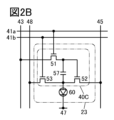
- FIG. 2B is a circuit diagram showing an example of a pixel configuration.
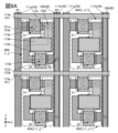
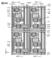
- 3A1 to 3A3 are plan views showing an example of the configuration of a display device.
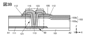
- FIG. 3B is a cross-sectional view showing a configuration example of a display device.
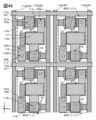
- FIG. 4A is a plan view showing a configuration example of a display device.
- FIG. 4B is a cross-sectional view showing a configuration example of a display device.
- FIG. 4A is a plan view showing a configuration example of a display device.
- FIG. 4B is a cross-sectional view showing a configuration example of a display device.
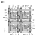
- FIG. 5 is a plan view showing an example of the configuration of the display device.
- FIG. 6 is a cross-sectional view showing a configuration example of a display device.
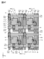
- 7A and 7B are plan views showing a configuration example of a display device.
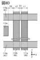
- 8A to 8D are plan views showing an example of the configuration of a display device.
- 9A to 9C are plan views showing an example of the configuration of a display device.
- FIG. 10 is a cross-sectional view showing a configuration example of a display device.
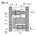
- 11A and 11B are plan views showing a configuration example of a display device.
- FIG. 12 is a plan view showing a configuration example of a display device.
- FIG. 13 is a cross-sectional view showing a configuration example of a display device.
- FIG. 14 is a plan view showing a configuration example of a display device.
- FIG. 15 is a cross-sectional view showing a configuration example of a display device.
- 16A to 16C are plan views showing an example of the configuration of a display device.
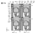
- 17A to 17C are plan views showing an example of the configuration of a display device.
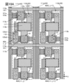
- FIG. 18A is a plan view showing a configuration example of a display device.
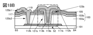
- FIG. 18B is a cross-sectional view showing a configuration example of a display device.
- FIG. 19 is a plan view showing a configuration example of a display device.
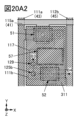
- FIG. 20A1 and FIG. 20A2 are plan views showing a configuration example of a display device.
- FIG. 20B is a cross-sectional view showing a configuration example of a display device.
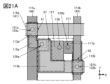
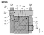
- FIG. 21A and 21B are plan views showing a configuration example of a display device.
- FIG. 22A is a plan view showing a configuration example of a display device.
- FIG. 22B is a cross-sectional view showing a configuration example of a display device.
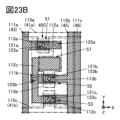
- 23A and 23B are plan views showing a configuration example of a display device.
- FIG. 24A is a plan view showing a configuration example of a display device.
- FIG. 24B is a cross-sectional view showing a configuration example of a display device.
- 25A to 25C are plan views showing an example of the configuration of a display device.
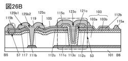
- FIG. 26A is a plan view showing a configuration example of a display device.
- FIG. 26B is a cross-sectional view showing a configuration example of a display device.
- FIG. 26A is a plan view showing a configuration example of a display device.
- FIG. 26B is a cross-sectional view showing a configuration example of a display device.
- FIG. 27 is a plan view showing a configuration example of a display device.
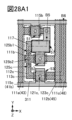
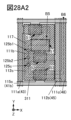
- 28A1 and 28A2 are plan views showing an example of the configuration of a display device.
- FIG. 28B is a cross-sectional view showing a configuration example of a display device.
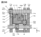
- 29A and 29B are plan views showing a configuration example of a display device.
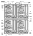
- FIG. 30A is a plan view showing a configuration example of a display device.
- FIG. 30B is a cross-sectional view showing a configuration example of a display device.
- FIG. 31A is a plan view showing a configuration example of a display device.
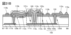
- FIG. 31B is a cross-sectional view showing a configuration example of a display device.
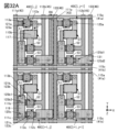
- FIG. 32A is a plan view showing a configuration example of a display device.
- FIG. 32B is a cross-sectional view showing a configuration example of a display device.
- FIG. 33 is a plan view showing a configuration example of a display device.
- FIG. 34A is a plan view showing a configuration example of a display device.
- FIG. 34B is a cross-sectional view showing a configuration example of a display device.
- FIG. 35A is a plan view showing a configuration example of a display device.
- FIG. 35B is a cross-sectional view showing a configuration example of a display device.
- FIG. 36 is a plan view showing a configuration example of a display device.
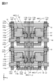
- FIG. 37 is a plan view showing a configuration example of a display device.
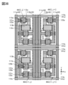
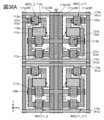
- FIG. 38A is a plan view showing a configuration example of a display device.
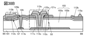
- FIG. 38B is a cross-sectional view showing a configuration example of a display device.
- FIG. 39A is a plan view showing a configuration example of a display device.
- FIG. 39B is a cross-sectional view showing a configuration example of a display device.
- FIG. 40A and FIG. 40B are plan views showing a configuration example of a display device.
- FIG. 41A is a plan view showing a configuration example of a display device.
- FIG. 41B is a cross-sectional view showing a configuration example of a display device.
- FIG. 42A is a plan view showing a configuration example of a display device.
- FIG. 42B is a cross-sectional view showing a configuration example of a display device.
- FIG. 43 is a plan view showing a configuration example of a display device.
- FIG. 44 is a plan view showing a configuration example of a display device.
- FIG. 45 is a plan view showing a configuration example of a display device.
- FIG. 46 is a plan view showing a configuration example of a display device.
- FIG. 47 is a plan view showing a configuration example of a display device.
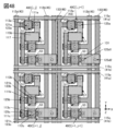
- FIG. 48 is a plan view showing a configuration example of a display device.
- FIG. 49 is a plan view showing a configuration example of a display device.
- FIG. 50 is a plan view showing a configuration example of a display device.
- FIG. 51 is a plan view showing a configuration example of a display device.
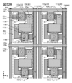
- FIG. 52A is a plan view showing a configuration example of a display device.
- FIG. 52A is a plan view showing a configuration example of a display device.
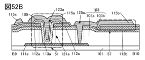
- FIG. 52B is a cross-sectional view showing a configuration example of a display device.
- FIG. 53 is a plan view showing a configuration example of a display device.
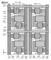
- FIG. 54A is a plan view showing a configuration example of a display device.
- FIG. 54B is a cross-sectional view showing a configuration example of a display device.
- FIG. 55 is a plan view showing a configuration example of a display device.
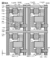
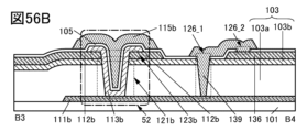
- FIG. 56A is a plan view showing a configuration example of a display device.
- FIG. 56B is a cross-sectional view showing a configuration example of a display device.
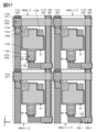
- FIG. 57 is a plan view showing a configuration example of a display device.
- FIG. 58 is a plan view showing a configuration example of a display device.
- FIG. 59 is a plan view showing a configuration example of a display device.
- FIG. 60 is a plan view showing a configuration example of a display device.
- FIG. 61 is a plan view showing a configuration example of a display device.
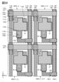
- FIG. 62A is a plan view showing a configuration example of a display device.
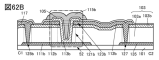
- FIG. 62B is a cross-sectional view showing a configuration example of a display device.
- FIG. 63 is a plan view showing a configuration example of a display device.
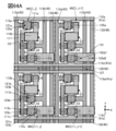
- FIG. 64A is a plan view showing a configuration example of a display device.
- FIG. 64B is a cross-sectional view showing a configuration example of a display device.
- FIG. 65 is a plan view showing a configuration example of a display device.
- FIG. 66A is a plan view showing a configuration example of a display device.
- FIG. 66B is a cross-sectional view showing a configuration example of a display device.
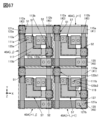
- FIG. 67 is a plan view showing a configuration example of a display device.
- FIG. 68A is a plan view showing a configuration example of a display device.
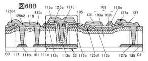
- FIG. 68B is a cross-sectional view showing a configuration example of a display device.
- FIG. 69 is a plan view showing a configuration example of a display device.
- FIG. 70A is a plan view showing a configuration example of a display device.
- FIG. 70B is a cross-sectional view showing a configuration example of a display device.
- FIG. 71 is a plan view showing a configuration example of a display device.
- FIG. 72 is a plan view showing a configuration example of a display device.
- FIG. 73 is a plan view showing a configuration example of a display device.
- FIG. 74A is a plan view showing a configuration example of a display device.
- FIG. 74B is a cross-sectional view showing a configuration example of a display device.
- FIG. 75 is a plan view showing a configuration example of a display device.
- FIG. 76 is a plan view showing a configuration example of a display device.
- FIG. 77 is a plan view showing a configuration example of a display device.
- FIG. 78A is a plan view showing a configuration example of a display device.
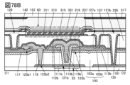
- FIG. 78B is a cross-sectional view showing a configuration example of a display device.
- FIG. 79A is a plan view showing a configuration example of a display device.
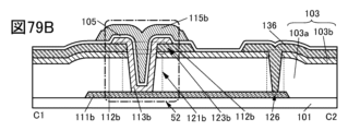
- FIG. 79B is a cross-sectional view showing a configuration example of a display device.
- FIG. 80 is a plan view showing a configuration example of a display device.
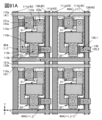
- FIG. 81A is a plan view showing a configuration example of a display device.
- FIG. 81B is a cross-sectional view showing a configuration example of a display device.
- FIG. 82 is a plan view showing a configuration example of a display device.
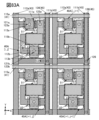
- FIG. 83A is a plan view showing a configuration example of a display device.
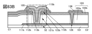
- FIG. 83B is a cross-sectional view showing a configuration example of a display device.
- FIG. 84 is a plan view showing a configuration example of a display device.
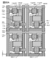
- FIG. 85A is a plan view showing a configuration example of a display device.
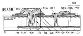
- FIG. 85B is a cross-sectional view showing a configuration example of a display device.
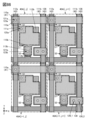
- FIG. 86 is a plan view showing a configuration example of a display device.
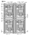
- FIG. 87A is a plan view showing a configuration example of a display device.
- FIG. 87B is a cross-sectional view showing a configuration example of a display device.
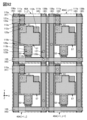
- FIG. 88 is a plan view showing a configuration example of a display device.
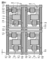
- FIG. 89 is a plan view showing a configuration example of a display device.
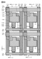
- FIG. 90 is a plan view showing a configuration example of a display device.
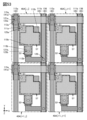
- FIG. 91 is a plan view showing a configuration example of a display device.
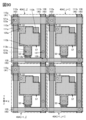
- FIG. 91 is a plan view showing a configuration example of a display device.
- FIG. 92 is a plan view showing a configuration example of a display device.
- FIG. 93A is a plan view showing a configuration example of a display device.
- FIG. 93B is a cross-sectional view showing a configuration example of a display device.
- FIG. 94 is a plan view showing a configuration example of a display device.
- FIG. 95 is a plan view showing a configuration example of a display device.
- FIG. 96 is a plan view showing a configuration example of a display device.
- FIG. 97 is a plan view showing a configuration example of a display device.
- FIG. 98 is a plan view showing a configuration example of a display device.
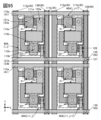
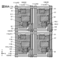
- FIG. 99A is a plan view showing a configuration example of a display device.
- FIG. 99A is a plan view showing a configuration example of a display device.
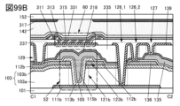
- FIG. 99B is a cross-sectional view showing a configuration example of a display device.
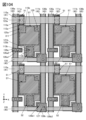
- FIG. 100 is a plan view showing a configuration example of a display device.
- FIG. 101 is a plan view showing a configuration example of a display device.
- FIG. 102 is a plan view showing a configuration example of a display device.
- FIG. 103 is a plan view showing a configuration example of a display device.
- FIG. 104 is a plan view showing a configuration example of a display device.
- 105A to 105C are circuit diagrams showing examples of pixel configurations.
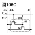
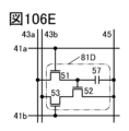
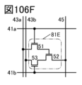
- FIG. 106A is a block diagram showing a configuration example of a storage device.
- 106B to 106F are circuit diagrams showing configuration examples of memory cells.
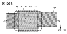
- FIG. 107A to 107C are plan views showing an example of the configuration of a display device.
- FIG. 108A is a plan view showing a configuration example of a display device.
- FIG. 108B is a cross-sectional view showing a configuration example of a display device.
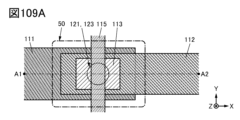
- FIG. 109A is a plan view showing a configuration example of a display device.
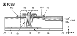
- FIG. 109B is a cross-sectional view showing a configuration example of a display device.
- FIG. 110A is a plan view showing a configuration example of a display device.
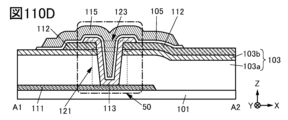
- FIGS. 110B to 110D are cross-sectional views illustrating a configuration example of a display device.
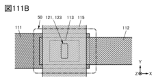
- 111A and 111B are plan views showing a configuration example of a display device.
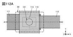
- FIG. 112A and 112B are plan views showing an example of the configuration of a display device.
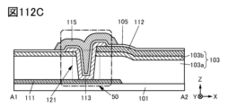
- FIG. 112C is a cross-sectional view showing a configuration example of a display device.
- FIG. 113A is a plan view showing a configuration example of a display device.
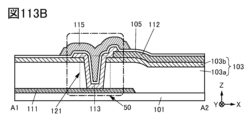
- FIG. 113B is a cross-sectional view showing a configuration example of a display device.
- FIG. 114A is a plan view showing a configuration example of a display device.
- FIG. 114B is a cross-sectional view showing a configuration example of a display device.
- FIG. 115A is a plan view showing a configuration example of a display device.
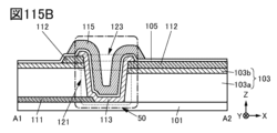
- FIG. 115B is a cross-sectional view showing a configuration example of a display device.
- FIG. 116B are plan views showing a configuration example of a display device.
- FIG. 116C is a cross-sectional view showing a configuration example of a display device.
- FIG. 117A is a plan view showing a configuration example of a display device.
- FIG. 117B is a cross-sectional view showing a configuration example of a display device.
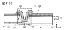
- FIG. 118A is a plan view showing a configuration example of a display device.
- FIG. 118B is a cross-sectional view showing a configuration example of a display device.
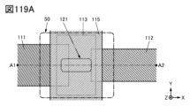
- FIG. 119A and FIG. 119B are plan views showing a configuration example of a display device.
- 120A and 120B are plan views showing a configuration example of a display device.
- FIG. 120C is a cross-sectional view showing a configuration example of a display device.
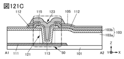
- FIG. 121A is a plan view showing a configuration example of a display device.
- FIG. 121B and FIG. 121C are cross-sectional views showing an example of the configuration of a display device.
- FIG. 122A and FIG. 122B are cross-sectional views showing a configuration example of a display device.
- FIG. 123A and FIG. 123B are cross-sectional views showing a configuration example of a display device.
- FIG. 124A and FIG. 124B are cross-sectional views showing a configuration example of a display device.
- FIG. 125A is a plan view showing a configuration example of a display device.
- 125B is a cross-sectional view showing a configuration example of a display device.
- 126A and 126B are plan views showing a configuration example of a display device.
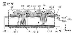
- FIG. 127A is a plan view showing a configuration example of a display device.
- FIG. 127B is a cross-sectional view showing a configuration example of a display device.
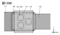
- 128A to 128C are plan views showing an example of the configuration of a display device.
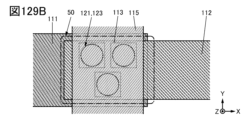
- 129A to 129C are plan views showing an example of the configuration of a display device.
- 130A and 130B are plan views showing a configuration example of a display device.
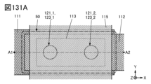
- FIG. 131A is a plan view showing a configuration example of a display device.
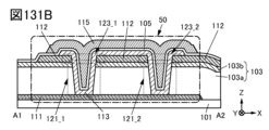
- FIG. 131B is a cross-sectional view showing a configuration example of a display device.
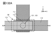
- FIG. 132A is a plan view showing a configuration example of a display device.
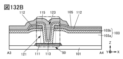
- FIG. 132B is a cross-sectional view showing a configuration example of a display device.
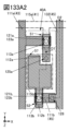
- FIG. 133A1 and FIG. 133A2 are plan views showing a configuration example of a display device.
- FIG. 133B is a cross-sectional view showing a configuration example of a display device.
- FIG. 134A1 and FIG. 134A2 are plan views showing a configuration example of a display device.
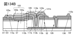
- FIG. 134B is a cross-sectional view showing a configuration example of a display device.
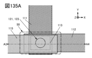
- 135A to 135C are plan views showing an example of the configuration of a display device.
- FIG. 136A and FIG. 136B are plan views showing a configuration example of a display device.
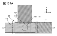
- FIG. 137A is a plan view showing a configuration example of a display device.
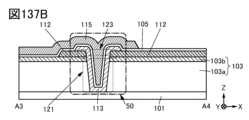
- FIG. 137B is a cross-sectional view showing a configuration example of a display device.
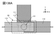
- 138A and 138B are plan views showing an example of the configuration of a display device.
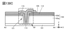
- FIG. 138C is a cross-sectional view showing a configuration example of a display device.
- FIG. 139A is a plan view showing a configuration example of a display device.
- FIG. 139B is a cross-sectional view showing a configuration example of a display device.
- FIG. 140A is a plan view showing a configuration example of a display device.
- FIG. 140A is a plan view showing a configuration example of a display device.
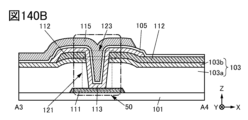
- FIG. 140B is a cross-sectional view showing a configuration example of a display device.
- FIG. 141A is a plan view showing a configuration example of a display device.
- FIG. 141B is a cross-sectional view showing a configuration example of a display device.
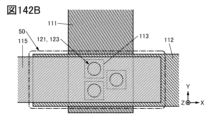
- 142A to 142C are plan views showing an example of the configuration of a display device.
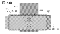
- 143A to 143C are plan views showing an example of the configuration of a display device.
- FIG. 144A and FIG. 144B are plan views showing a configuration example of a display device.
- FIG. 145A is a plan view showing a configuration example of a display device.
- FIG. 145B is a cross-sectional view showing a configuration example of a display device.
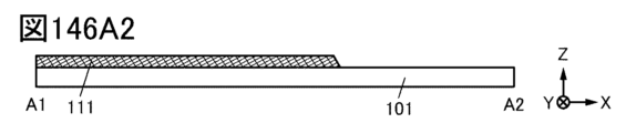
- 146A1 and 146B1 are plan views illustrating an example of a method for manufacturing a display device.
- 146A2 and 146B2 are cross-sectional views illustrating an example of a method for manufacturing a display device.
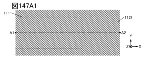
- 147A1 and 147B1 are plan views illustrating an example of a method for manufacturing a display device.
- 147A2 and 147B2 are cross-sectional views illustrating an example of a method for manufacturing a display device.
- 148A1 and 148B1 are plan views illustrating an example of a method for manufacturing a display device.
- 148A2 and 148B2 are cross-sectional views illustrating an example of a method for manufacturing a display device.
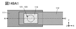
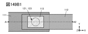
- 149A1 and 149B1 are plan views illustrating an example of a method for manufacturing a display device.
- 149A2 and 149B2 are cross-sectional views illustrating an example of a method for manufacturing a display device.
- 150A1 and 150B1 are plan views showing an example of a method for manufacturing a display device.
- 150A2 and 150B2 are cross-sectional views illustrating an example of a method for manufacturing a display device.
- FIG. 151 is a perspective view showing a configuration example of a display device.
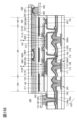
- FIG. 152 is a cross-sectional view showing a configuration example of a display device.
- FIG. 153 is a cross-sectional view showing a configuration example of a display device.
- FIG. 154 is a cross-sectional view showing a configuration example of a display device.
- FIG. 155 is a cross-sectional view showing a configuration example of a display device.
- FIG. 156 is a cross-sectional view showing a configuration example of a display device.
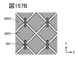
- FIG. 157A is a perspective view showing a configuration example of a display device.
- FIG. 157B is a plan view showing a configuration example of a touch sensor.
- FIG. 158 is a cross-sectional view showing a configuration example of a display device.
- FIG. 159 is a cross-sectional view showing a configuration example of a display device.
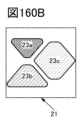
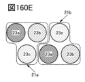
- 160A to 160G are plan views showing examples of pixel configurations.
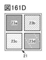
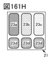
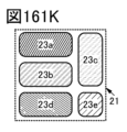
- 161A to 161K are plan views showing examples of pixel configurations.
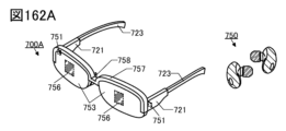
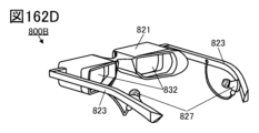
- 162A to 162D are diagrams illustrating an example of an electronic device.
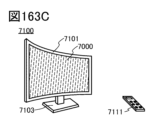
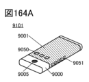
- 163A to 163F are diagrams illustrating an example of an electronic device.
- the same parts or parts having similar functions are designated by the same reference numerals in different drawings, and repeated explanation thereof will be omitted.
- the hatching pattern may be the same and no particular reference numeral may be attached.
- a plurality of layers that can be formed in the same process may be provided with the same hatching pattern.
- film and layer can be interchanged depending on the situation or circumstances. For example, it may be possible to change the term “conductive layer” to the term “conductive film.” Or, for example, it may be possible to change the term “insulating film” to the term “insulating layer.”
- electrode and “wiring” do not functionally limit these components.
- an “electrode” may be used as part of a “wiring” and vice versa.
- the term “electrode” or “wiring” includes cases where a plurality of “electrodes” or “wirings” are formed integrally.
- SBS Side By Side
- materials and configurations can be optimized for each light emitting element, which increases the degree of freedom in selecting materials and configurations, making it easier to improve brightness and reliability.
- a light emitting element has an EL layer between a pair of electrodes.
- the EL layer has at least a light emitting layer.
- the layers (also referred to as functional layers) included in the EL layer include a light emitting layer, a carrier injection layer (a hole injection layer and an electron injection layer), a carrier transport layer (a hole transport layer and an electron transport layer), and Examples include carrier block layers (hole block layers and electron block layers).
- the carrier injection layer, carrier transport layer, and carrier block layer may not be clearly distinguishable depending on their respective cross-sectional shapes or characteristics.
- one layer may serve as two or three functions among a carrier injection layer, a carrier transport layer, and a carrier block layer.
- a light receiving element (also referred to as a light receiving device) has an active layer that functions as at least a photoelectric conversion layer between a pair of electrodes.
- a tapered shape refers to a shape in which at least a part of the side surface of a structure is inclined with respect to a substrate surface or a surface to be formed.
- a region where the angle between the inclined side surface and the substrate surface or the surface to be formed also referred to as a taper angle
- the side surface of the structure, the substrate surface, and the surface to be formed do not necessarily have to be completely flat, and may be substantially planar with a minute curvature or substantially planar with minute irregularities.
- the outermost portion of the side surface of the layer is referred to as the end of the layer, unless otherwise specified.
- the bottom end of a layer is located outside the top end, the bottom end of the layer is simply referred to as an end unless otherwise specified.
- metal oxide refers to a metal oxide in a broad sense. Metal oxides are classified into oxide insulators, oxide conductors (including transparent oxide conductors), oxide semiconductors (also referred to as oxide semiconductors or simply OS), and the like. For example, when a metal oxide is used for a semiconductor layer of a transistor, the metal oxide is sometimes referred to as an oxide semiconductor. That is, when it is described as an OS transistor, it can be paraphrased as a transistor including a metal oxide or an oxide semiconductor. Note that metal oxides containing nitrogen may also be collectively referred to as metal oxides. Furthermore, a metal oxide containing nitrogen may also be referred to as a metal oxynitride.
- One embodiment of the present invention relates to a display device that includes a display portion, a scanning line driver circuit, a signal line driver circuit, and a power supply circuit, and in which pixels are arranged in a matrix in the display portion.
- the pixel is provided with a first transistor and a second transistor.
- the first transistor may be a transistor in which the first semiconductor layer is provided inside an opening formed in an interlayer insulating layer on the substrate, and the second transistor may be a transistor formed in an interlayer insulating layer on the substrate.
- the transistor may include a second semiconductor layer provided inside an opening different from the opening described above.
- the channel length direction of the transistor can be set along the side surface of the interlayer insulating layer in the opening. Therefore, the channel length is not affected by the performance of the exposure apparatus used for manufacturing the transistor, so the channel length can be made smaller than the limit resolution of the exposure apparatus.
- the first conductive layer provided under the opening is used as one of the source electrode and the drain electrode of the first transistor.
- an interlayer insulating layer is provided on the first conductive layer, and an opening is provided in the interlayer insulating layer so as to reach the first conductive layer.
- the first semiconductor layer is provided so as to have a region in contact with the first conductive layer inside the opening.
- a second conductive layer surrounding the outer periphery of the opening in plan view is used as the other of the source electrode and the drain electrode of the first transistor.
- a gate insulating layer is provided over the first semiconductor layer and the second conductive layer, and a third conductive layer functioning as a gate electrode of the first transistor is provided over the gate insulating layer.
- a plan view may be referred to as a top view. Further, the plan view may be called a top view.
- the second transistor can have a similar configuration to the first transistor.
- a fourth conductive layer provided under the opening is used as one of the source electrode and the drain electrode of the second transistor. Further, as the other of the source electrode and the drain electrode of the second transistor, a fifth conductive layer surrounding the outer periphery of the opening in plan view is used.
- the gate insulating layer is also provided on the second semiconductor layer and the fifth conductive layer, and a sixth conductive layer functioning as a gate electrode of the second transistor is provided on the gate insulating layer.
- the first conductive layer or the second conductive layer is electrically connected to the signal line drive circuit.
- the third conductive layer has a region extending in the row direction and is electrically connected to the scanning line drive circuit.
- the fifth conductive layer has a region extending in the column direction and is electrically connected to the power supply circuit. Since the third conductive layer has a region extending in the row direction and the fifth conductive layer has a region extending in the column direction, the third conductive layer and the fifth conductive layer have regions that overlap with each other. .
- the gate insulating layer is provided on the fifth conductive layer in a region where the third conductive layer and the fifth conductive layer overlap, and the third conductive layer is provided thereon. provided.
- the display device of one embodiment of the present invention can have high display quality.
- the fourth conductive layer instead of the fifth conductive layer may be electrically connected to the power supply circuit.
- the fourth conductive layer has a region extending in the column direction.
- the seventh conductive layer is provided so as to have a region overlapping with the fourth conductive layer.
- the seventh conductive layer has a region extending in the column direction, and has a region overlapping with a region of the fourth conductive layer extending in the column direction.
- the seventh conductive layer is provided in the same layer as the fifth conductive layer, that is, between the interlayer insulating layer and the gate insulating layer.
- the interlayer insulating layer has an opening that reaches the fourth conductive layer, and the fourth conductive layer and the seventh conductive layer are electrically connected inside the opening.
- the power supply circuit is electrically connected to the fourth conductive layer, and the fourth conductive layer is electrically connected to the seventh conductive layer, so that the fourth and seventh conductive layers are electrically connected to the power supply circuit. connected to.
- not only the fourth conductive layer but also the seventh conductive layer provided in a layer different from the fourth conductive layer can function as a wiring for electrically connecting the power supply circuit and the pixel.
- the display device of one embodiment of the present invention can have high display quality.
- FIG. 1A is a block diagram illustrating a configuration example of a display device 10, which is a display device of one embodiment of the present invention.
- the display device 10 includes a display section 20 , a scanning line drive circuit 11 , a signal line drive circuit 13 , and a power supply circuit 15 .
- the display section 20 has a plurality of pixels 21 arranged in a matrix. Note that the power supply circuit 15 may be provided outside the display device 10.
- the scanning line drive circuit 11 is electrically connected to the pixels 21 via wiring 41.
- the wiring 41 extends, for example, in the row direction of the matrix.
- the signal line drive circuit 13 is electrically connected to the pixel 21 via the wiring 43.
- the wiring 43 extends, for example, in the column direction of the matrix.
- Power supply circuit 15 is electrically connected to pixel 21 via wiring 45.
- all the pixels 21 can be electrically connected to the power supply circuit 15 via the same wiring 45.
- the wiring 41 and the wiring 43 are shown as straight lines, but one straight line is not necessarily one wiring, and a plurality of wirings may be represented as one straight line. In subsequent block diagrams, circuit diagrams, etc., a plurality of wiring lines may be represented by a single straight line. Also, in wirings other than the wiring 41 and the wiring 43, a plurality of wirings may be represented by one straight line.
- the pixel 21 has a display element, and can display an image on the display section 20 using the display element.
- a display element for example, a light emitting element can be used, and specifically, an organic EL element can be used. Further, a liquid crystal element (also referred to as a liquid crystal device) may be used as the display element.
- the scanning line drive circuit 11 has a function of selecting, for example, pixels 21 for writing image data on a row-by-row basis. Specifically, the scanning line drive circuit 11 can select the pixel 21 into which image data is to be written by outputting a signal to the wiring 41.
- the scanning line drive circuit 11 outputs the above-mentioned signal to the wiring 41 in the first row, for example, outputs the above-mentioned signal to the wiring 41 in the second row, and sequentially outputs the above-mentioned signal to the wiring 41 in the last row. By doing so, all pixels 21 can be selected. Therefore, the signal that the scanning line drive circuit 11 outputs to the wiring 41 is a scanning signal, and the wiring 41 can be called a scanning line.
- the signal line drive circuit 13 has a function of generating image data.
- Image data is supplied to the pixels 21 via wiring 43.
- image data can be written to all pixels 21 included in the row selected by the scanning line drive circuit 11.
- the image data can be expressed as a signal (image signal). Therefore, the wiring 43 can be called a signal line.
- the power supply circuit 15 has a function of generating a power supply potential and supplying it to the wiring 45.
- the power supply circuit 15 has a function of, for example, generating a high power supply potential (hereinafter also simply referred to as "high potential” or “VDD”) and supplying it to the wiring 45. Further, the power supply circuit 15 may have a function of generating a low power supply potential (hereinafter also simply referred to as "low potential” or "VSS"). Since the power supply potential is supplied to the wiring 45, the wiring 45 can be called a power supply line.
- the wiring 41 and the wiring 45 have an overlapping region with an insulating layer interposed therebetween.
- a parasitic capacitance 25 is formed between the wiring 41 and the wiring 45.
- the charges accumulated in the parasitic capacitance 25 can be supplied to the wiring 45. Therefore, the parasitic capacitance 25 can function as a bypass capacitor.
- the thinner the insulating layer between the wiring 41 and the wiring 45 is, the larger the capacitance value of the parasitic capacitance 25 becomes.
- the display device 10 can be a display device with high display quality.
- FIG. 1B is a plan view showing an example of the configuration of the pixel 21.
- Pixel 21 can have multiple sub-pixels 23.
- FIG. 1B shows an example in which the pixel 21 includes a sub-pixel 23R, a sub-pixel 23G, and a sub-pixel 23B.
- the planar shape of the subpixel shown in FIG. 1B corresponds to the planar shape of the light emitting region of the light emitting element. Note that in FIG.
- the subpixel 23R, the subpixel 23G, and the subpixel 23B have the same or approximately the same aperture ratio (which can also be called the size or the size of the light emitting region), but one embodiment of the present invention is not limited to this. .
- the aperture ratios of the sub-pixel 23R, the sub-pixel 23G, and the sub-pixel 23B can be determined as appropriate.
- the aperture ratios of the sub-pixel 23R, the sub-pixel 23G, and the sub-pixel 23B may be different from each other, or two or more may be equal or approximately equal.
- a stripe arrangement is applied as an arrangement method of the sub-pixels 23.
- an S stripe arrangement, a matrix arrangement, a delta arrangement, a Bayer arrangement, a pentile arrangement, or the like may be applied as an arrangement method for the sub-pixels 23.
- Embodiment 4 can be referred to for an example of the planar shape of the sub-pixels, the arrangement of the sub-pixels, and the like.
- the sub-pixel 23R, the sub-pixel 23G, and the sub-pixel 23B each exhibit different colors of light.
- the subpixel 23R, the subpixel 23G, and the subpixel 23B are subpixels of three colors: red (R), green (G), and blue (B), and yellow (Y), cyan (C), and magenta ( M) three-color sub-pixels, etc. may be mentioned.
- four or more sub-pixels 23 may be provided in the pixel 21.
- the pixel 21 may be provided with sub-pixels of four colors: R, G, B, and white (W).
- the display device 10 can display a full-color image on the display unit 20 because the pixel 21 has a plurality of sub-pixels 23 that emit light of different colors.
- the pixel 21 may be provided with sub-pixels for, for example, R, G, B, and infrared light (IR).
- the display unit 20 may be provided with a sensor, for example, the pixel 21 may be provided with a sensor.
- the display unit 20 may have a function as a fingerprint sensor.
- the display unit 20 may function as an optical or ultrasonic fingerprint sensor.
- FIG. 1C is a circuit diagram showing a configuration example of the sub-pixel 23.
- the subpixel 23 shown in FIG. 1C includes a pixel circuit 40A and a light emitting element 60.
- the pixel circuit 40A includes a transistor 51, a transistor 52, and a capacitor 57.
- the pixel circuit 40A is a 2Tr (transistor) 1C (capacitance) type pixel circuit.
- one of the source and drain of the transistor 51 is electrically connected to the wiring 43.
- the other of the source and drain of transistor 51 is electrically connected to the gate of transistor 52.
- the gate of transistor 52 is electrically connected to one electrode of capacitor 57.
- a gate of the transistor 51 is electrically connected to the wiring 41.
- One of the source and drain of the transistor 52 is electrically connected to the wiring 45.
- the other of the source and drain of the transistor 52 is electrically connected to the other electrode of the capacitor 57.
- the other electrode of the capacitor 57 is electrically connected to one electrode of the light emitting element 60.
- the other electrode of the light emitting element 60 is electrically connected to the wiring 47.
- one electrode of the light emitting element 60 is also referred to as a pixel electrode.
- the wiring 47 can be shared among all the sub-pixels 23, for example. Therefore, the other electrode of the light emitting element 60 can also be called a common electrode.
- the wiring 41 functions as a scanning line
- the wiring 43 functions as a signal line
- the wiring 45 functions as a power supply line.
- the wiring 47 functions as a power supply line, and for example, when the wiring 45 is supplied with a high power supply potential, the wiring 47 is supplied with a low power supply potential.
- the wiring 47 can be electrically connected to the power supply circuit 15, for example.
- the transistor 51 has a function as a switch and is also called a selection transistor.
- the transistor 51 has a function of controlling the conduction state and non-conduction state between the wiring 43 and the gate of the transistor 52 based on the potential of the wiring 41.
- the transistor 52 has a function of controlling the amount of current flowing through the light emitting element 60, and is also referred to as a drive transistor.
- Capacitor 57 has a function of holding the gate potential of transistor 52.
- the light emission brightness of the light emitting element 60 is controlled according to a potential corresponding to image data, which is supplied to the gate of the transistor 52. Specifically, when a high power supply potential is supplied to the wiring 45 and a low power supply potential is supplied to the wiring 47, the magnitude of the current flowing from the wiring 45 to the wiring 47 is controlled according to the gate potential of the transistor 52. Ru. Thereby, the luminance of the light emitting element 60 is controlled.
- OS transistors As the transistors 51 and 52.
- An OS transistor has higher field effect mobility than a transistor using, for example, amorphous silicon. Therefore, by using OS transistors as the transistors 51 and 52, the display device 10 can be driven at high speed.
- the OS transistor has a significantly small source-drain leakage current (also referred to as off-state current) in the off state. Therefore, by using an OS transistor as the transistor 51, the charges accumulated in the capacitor 57 can be held for a long period of time. Thereby, the image data written to the subpixel 23 can be retained for a long period of time, so that the frequency of refresh operations (rewriting of image data to the subpixel 23) can be reduced. Therefore, power consumption of the display device 10 can be reduced.
- the source-drain voltage of the transistor 52 which is a driving transistor. Since an OS transistor has a higher breakdown voltage between the source and drain than a transistor using silicon (also referred to as a Si transistor), a high voltage can be applied between the source and drain of the OS transistor. Therefore, by using an OS transistor as the transistor 52, the amount of current flowing through the light emitting element 60 can be increased, and the luminance of the light emitting element 60 can be increased.
- OS transistors can have smaller changes in source-drain current with respect to changes in gate-source voltage than Si transistors. Therefore, by using an OS transistor as the transistor 52, the current flowing between the source and the drain can be precisely determined by changing the voltage between the gate and the source. Therefore, the amount of current flowing through the light emitting element 60 can be finely controlled. Therefore, the brightness of the light emitted by the subpixel 23 can be finely controlled. Therefore, the number of gradations that can be expressed by the subpixel 23 can be increased.
- OS transistors are able to flow a more stable current (saturation current) than Si transistors even when the source-drain voltage gradually increases. can. Therefore, by using an OS transistor as the transistor 52, a stable current can be passed through the light emitting element 60 even if, for example, the current-voltage characteristics of the light emitting element 60 vary from one light emitting element 60 to another. That is, when the OS transistor is driven in the saturation region, the source-drain current does not substantially change even if the source-drain voltage is increased, so that the luminance of the light emitting element 60 can be stabilized.
- transistor 51 and the transistor 52 are n-channel transistors in FIG. 1C, one or both of the transistor 51 and the transistor 52 may be a p-channel transistor. The same applies to other transistors shown in this specification and the like.
- the light-emitting element 60 it is preferable to use, for example, an OLED (Organic Light Emitting Diode) or a QLED (Quantum-dot Light Emitting Diode).
- the light-emitting substance included in the light-emitting element 60 include a substance that emits fluorescence (fluorescent material), a substance that emits phosphorescence (phosphorescent material), and a substance that exhibits thermally activated delayed fluorescence (thermally activated delayed fluorescence (TADF). ) materials), and inorganic compounds (e.g. quantum dot materials).
- an LED such as a micro LED (Light Emitting Diode) can also be used.
- FIG. 1D is a circuit diagram showing a configuration example of the sub-pixel 23.
- the subpixel 23 shown in FIG. 1D includes a pixel circuit 40B and a liquid crystal element 69.
- the pixel circuit 40B includes a transistor 51 and a capacitor 57.
- the pixel circuit 40B is a 1Tr1C type pixel circuit.
- one of the source and drain of the transistor 51 is electrically connected to the wiring 43.
- the other of the source and drain of the transistor 51 is electrically connected to one electrode of the capacitor 57.
- One electrode of the capacitor 57 is electrically connected to one electrode of the liquid crystal element 69.
- a gate of the transistor 51 is electrically connected to the wiring 41.
- the other electrode of the capacitor 57 and the other electrode of the liquid crystal element 69 are electrically connected to the wiring 45.
- one electrode of the liquid crystal element 69 is also referred to as a pixel electrode.
- the other electrode of the liquid crystal element 69 may be referred to as a common electrode.
- the wiring 45 can be supplied with, for example, a ground potential.
- the transistor 51 has a function as a switch, and has a function of controlling the conduction state and non-conduction state between the wiring 43 and one electrode of the liquid crystal element 69 based on the potential of the wiring 41. have By turning on the transistor 51, image data is written into the pixel circuit 40B, and by turning the transistor 51 off, the written image data is held.
- the capacitor 57 has a function of holding the potential of one electrode of the liquid crystal element 69.
- the alignment state of liquid crystal molecules included in the liquid crystal element 69 is controlled in accordance with a potential corresponding to image data that is supplied to one electrode of the liquid crystal element 69.
- the modes of the liquid crystal element 69 include, for example, TN (Twisted Nematic) mode, STN (Super-Twisted Nematic) mode, VA (Vertical Alignment) mode, and ASM (Axially Symmetric Alignment).
- OCB Optically Compensated Birefringence
- FLC Fluorescence Liquid Crystal
- AFLC AntiFerroelectric Liquid Crystal
- MVA Multidomain Vertical Alignment
- PVA Powerned Vertical Alignment
- IPS In Plane Switching
- FFS Fluor Field Switching
- TBA Transverse Bend Alignment
- ECB Electrically Controlled Birefringence
- PDLC Polymer Dispersed Liquid Crystal
- PNLC Polymer Network
- FIG. 2A is a block diagram showing a configuration example of the display device 10, and is a modification of the display device 10 shown in FIG. 1A.
- the display device 10 shown in FIG. 2A differs from the display device 10 shown in FIG. 1A in that the wiring 41 includes a wiring 41a and a wiring 41b, and that a reference potential generation circuit 17 is provided.
- a parasitic capacitance 25 is formed between the wiring 41a and the wiring 45 and between the wiring 41b and the wiring 45.
- the reference potential generation circuit 17 is electrically connected to the pixel 21 via a wiring 48.
- all the pixels 21 can be electrically connected to the reference potential generation circuit 17 via the same wiring 48.
- the reference potential generation circuit 17 has a function of generating a reference potential for correcting variations in the gate-source potential of each transistor 52, for example, and supplying it to the wiring 48. Since the potential of the wiring 48 is the reference potential, the wiring 48 can be called a reference potential line.
- the reference potential generation circuit 17 may also be referred to as a power supply circuit. Further, the power supply circuit 15 and the reference potential generation circuit 17 may be combined into one circuit. For example, the reference potential generation circuit 17 may be included in the power supply circuit 15.
- FIG. 2B is a circuit diagram showing a configuration example of the subpixel 23 included in the pixel 21 shown in FIG. 2A.
- the subpixel 23 shown in FIG. 2B includes a pixel circuit 40C and a light emitting element 60.
- the pixel circuit 40C has a configuration in which a transistor 53 is added to the pixel circuit 40A.
- the pixel circuit 40C is a 3Tr1C type pixel circuit.
- the gate of the transistor 51 is electrically connected to the wiring 41a.
- One of the source and drain of the transistor 53 is electrically connected to the other source and drain of the transistor 52, the other electrode of the capacitor 57, and one electrode of the light emitting element 60.
- the other of the source and drain of the transistor 53 is electrically connected to the wiring 48.
- a gate of the transistor 53 is electrically connected to the wiring 41b.
- the transistor 53 has a function as a switch, and has a function of controlling a conductive state and a non-conductive state between the wiring 48 and one electrode of the light emitting element 60 based on the potential of the wiring 41b. For example, a reference potential is supplied to the wiring 48.
- the reference potential of the wiring 48 supplied via the transistor 53 can suppress variations in the gate-source potential of the transistor 52 for each transistor 52 .
- the wiring 48 can function as a monitor line for outputting the current flowing through the transistor 52 or the current flowing through the light emitting element 60 to the outside of the pixel 21.
- the current output to the wiring 48 can be converted into a potential by, for example, a source follower circuit. Alternatively, it can be converted into a digital signal using, for example, an A-D converter.
- the display device 10 does not need to include the reference potential generation circuit 17.
- the pixels 21 can be electrically connected to different wiring 48 for each column.
- an OS transistor As described above, an OS transistor has higher field effect mobility than a transistor using, for example, amorphous silicon. Therefore, by using an OS transistor as the transistor 53, the display device 10 can be driven at high speed.
- FIG. 3A1 is a plan view illustrating a configuration example of a semiconductor device included in a display device according to one embodiment of the present invention, and specifically, a transistor 50, which is a transistor included in a display device according to one embodiment of the present invention, and its surroundings.
- FIG. 3 is a plan view showing a configuration example.
- FIG. 3B is a sectional view taken along the dashed line A1-A2 shown in FIG. 3A1. Note that in FIG. 3A1, some constituent elements of the transistor 50, such as an insulating layer, are omitted. In the plan view of the transistor, some constituent elements such as an insulating layer are omitted in subsequent drawings as well.
- the transistor 50 can be applied to, for example, a transistor included in the pixel 21.
- the transistor 50 can be applied to the transistors 51 to 54 and the transistors 61 to 66.
- the transistor 50 may be applied to at least some of the transistors included in the scanning line drive circuit 11, the transistors included in the signal line drive circuit 13, the transistors included in the power supply circuit 15, and the transistors included in the reference potential generation circuit 17. good.
- Transistor 50 is provided on substrate 101.
- the transistor 50 includes a conductive layer 111, a conductive layer 112, a semiconductor layer 113, an insulating layer 105, and a conductive layer 115.
- FIG. 3A1 shows an example in which the conductive layer 112 extends in a direction parallel to the conductive layer 111 and extends in a direction perpendicular to the conductive layer 115.
- the direction in which the conductive layer 112 extends is defined as the X direction, as indicated by the coordinate axes. Further, a direction perpendicular to the X direction and parallel to, for example, the top surface of the substrate 101 (also referred to as the surface of the substrate 101) is a Y direction, and a direction perpendicular to the top surface of the substrate 101 is a Z direction.
- the definitions of the X direction, Y direction, and Z direction are shown using coordinate axes, but the definitions may be the same as or different from the definitions in FIGS. 3A1 and 3B.
- the X direction, Y direction, and Z direction can be directions perpendicular to each other. Further, the X direction and the Y direction may be parallel to the upper surface of the substrate (also referred to as the surface of the substrate), and the Z direction may be perpendicular to the upper surface of the substrate.
- the conductive layer 111 functions as either a source electrode or a drain electrode of the transistor 50.
- the conductive layer 112 functions as the other of the source electrode and the drain electrode of the transistor 50.
- the insulating layer 105 functions as a gate insulating layer of the transistor 50.
- the conductive layer 115 functions as a gate electrode of the transistor 50.
- the entire region between the source electrode and the drain electrode that overlaps with the gate electrode via the gate insulating layer functions as a channel formation region. Further, in the semiconductor layer 113, a region in contact with the source electrode functions as a source region, and a region in contact with the drain electrode functions as a drain region.
- a conductive layer 111 is provided over the substrate 101 , an insulating layer 103 is provided over the substrate 101 and the conductive layer 111 , and a conductive layer 112 is provided over the insulating layer 103 .
- the insulating layer 103 can function as an interlayer insulating layer.
- the conductive layer 111 and the conductive layer 112 have a region where they overlap with each other with the insulating layer 103 in between.
- the thickness of the insulating layer 103 functioning as an interlayer insulating layer can be made thicker than the thickness of the insulating layer 105 functioning as a gate insulating layer of the transistor 50.
- the insulating layer 103 has an opening 121 that reaches the conductive layer 111.
- the conductive layer 112 has an opening 123 that reaches the opening 121 . That is, the opening 123 has a region that overlaps with the opening 121. Further, the opening 123 has a region overlapping with the conductive layer 111.
- the conductive layer 112 is not provided inside the opening 121. In other words, it is preferable that the conductive layer 112 not be in contact with the side surface of the insulating layer 103 on the opening 121 side.
- FIG. 3A1 shows a conductive layer 111, a conductive layer 112, a semiconductor layer 113, a conductive layer 115, an opening 121, and an opening 123 as components of the transistor 50.
- FIG. 3A2 shows the conductive layer 111, the conductive layer 112, the semiconductor layer 113, the opening 121, and the opening 123.
- FIG. 3A3 shows the conductive layer 111, the conductive layer 112, the opening 121, and the opening 123.
- the conductive layer 112 has an opening 123 in a region overlapping with the conductive layer 111.
- the conductive layer 112 can be configured to cover the entire outer periphery of the opening 121 in plan view.
- the conductive layer 112 is not provided inside the opening 121. In other words, it is preferable that the conductive layer 112 not be in contact with the side surface of the insulating layer 103 on the opening 121 side.
- 3A1, 3A2, and 3A3 each show an example in which the opening 121 and the opening 123 are circular in plan view.
- the planar shape of the opening 121 and the opening 123 circular, it is possible to improve the processing accuracy when forming the opening 121 and the opening 123, and to form the opening 121 and the opening 123 of minute size. can.
- circular is not limited to a perfect circle.
- the planar shape of the opening 121 and the opening 123 may be, for example, an ellipse.
- FIG. 3B shows an example in which the end of the conductive layer 112 on the opening 123 side matches or approximately matches the end of the insulating layer 103 on the opening 121 side. It can be said that the planar shape of the opening 123 matches or approximately matches the planar shape of the opening 121. Note that in this specification and the like, the end of the conductive layer 112 on the opening 123 side and the end of the opening 123 refer to the lower end of the conductive layer 112 on the opening 123 side. The lower surface of the conductive layer 112 refers to the surface on the insulating layer 103 side.
- the end of the insulating layer 103 on the opening 121 side and the end of the opening 121 refer to the end of the upper surface of the insulating layer 103 on the opening 121 side.
- the upper surface of the insulating layer 103 refers to the surface on the conductive layer 112 side.
- the planar shape of the opening 123 refers to the planar shape of the lower end of the conductive layer 112 on the opening 123 side.
- the planar shape of the opening 121 refers to the planar shape of the upper end of the insulating layer 103 on the opening 121 side.
- the ends match or approximately match, it can also be said that the ends are aligned or substantially aligned.
- the edges are aligned or approximately aligned, and when the planar shapes are aligned or approximately aligned, at least a portion of the outlines of the laminated layers overlap in plan view. It can be said. For example, this includes a case where the upper layer and the lower layer are processed using the same mask pattern or partially the same mask pattern. However, strictly speaking, the outlines do not overlap, and the upper layer may be located inside the lower layer, or the upper layer may be located outside the lower layer, and in this case, the edges are roughly aligned, or the planar shape It is said that they roughly match.
- the opening 121 can be formed using, for example, the resist mask used to form the opening 123. Specifically, first, a conductive layer 111 is formed on the substrate 101, an insulating layer 103 is formed on the substrate 101 and the conductive layer 111, and a conductive film that will become the conductive layer 112 in a later step is formed on the insulating layer 103. and a resist mask on the conductive film. Then, after forming the opening 123 in the conductive film using the resist mask, the opening 121 is formed in the insulating layer 103 using the resist mask, so that the end of the opening 121 and the opening 123 are connected. The ends can be coincident or approximately coincident. With such a configuration, the process can be simplified.
- the semiconductor layer 113 is provided so as to cover the openings 121 and 123 and have a region located inside the openings 121 and 123.
- the semiconductor layer 113 has a shape that follows the top and side surfaces of the conductive layer 112 , the side surfaces of the insulating layer 103 , and the top surface of the conductive layer 111 .
- the semiconductor layer 113 has a region in contact with, for example, the top surface and side surfaces of the conductive layer 112, the side surfaces of the insulating layer 103, and the top surface of the conductive layer 111.
- the semiconductor layer 113 preferably covers the end of the conductive layer 112 on the opening 123 side.
- FIG. 3B shows a configuration in which the end of the semiconductor layer 113 is located on the conductive layer 112. It can also be said that the end of the semiconductor layer 113 is in contact with the upper surface of the conductive layer 112.
- the semiconductor layer 113 is shown to have a single layer structure in FIG. 3B, one embodiment of the present invention is not limited to this.
- the semiconductor layer 113 may have a stacked structure of two or more layers.
- the insulating layer 105 functioning as a gate insulating layer of the transistor 50 is provided so as to cover the opening 121 and the opening 123 and have a region located inside the opening 121 and the opening 123.
- the insulating layer 105 is provided over the semiconductor layer 113, the conductive layer 112, and the insulating layer 103.
- the insulating layer 105 can have a region in contact with the top surface and side surfaces of the semiconductor layer 113, the top surface and side surfaces of the conductive layer 112, and the top surface of the insulating layer 103.
- the insulating layer 105 has a shape that follows the top surface of the insulating layer 103, the top surface and side surfaces of the conductive layer 112, and the top surface and side surfaces of the semiconductor layer 113.
- the conductive layer 115 that functions as a gate electrode of the transistor 50 is provided over the insulating layer 105 and can have a region in contact with the top surface of the insulating layer 105.
- the conductive layer 115 has a region overlapping with the semiconductor layer 113 with the insulating layer 105 interposed therebetween.
- the conductive layer 115 has a region located inside the opening 121 and a region located inside the opening 123, and has an insulating layer 105 sandwiched between it and the semiconductor layer 113. It is provided so as to have areas facing each other. Further, in the example illustrated in FIG. 3B, the conductive layer 115 has a region overlapping with the conductive layer 111 and the conductive layer 112 with the insulating layer 105 and the semiconductor layer 113 interposed therebetween. Further, the conductive layer 115 covers the entire semiconductor layer 113.
- a gate electric field can be applied to the entire semiconductor layer 113, so the electrical characteristics of the transistor 50 can be improved, and, for example, the on-state current of the transistor can be increased.
- the insulating layer 103 in addition to the insulating layer 105 that functions as a gate insulating layer between the conductive layer 111 and the conductive layer 115, the insulating layer provided between the conductive layer 111 and the conductive layer 115 can be Compared to the case where only the insulating layer 103 is used, the parasitic capacitance formed by the conductive layer 111 and the conductive layer 115 is reduced.
- the transistor 50 is a so-called top-gate transistor that has a gate electrode above the semiconductor layer 113. Furthermore, since the lower surface of the semiconductor layer 113 has a region in contact with the source electrode and the drain electrode, it can be called a TGBC (Top Gate Bottom Contact) transistor.
- TGBC Top Gate Bottom Contact
- FIG. 4A is an enlarged plan view showing a configuration example of the transistor 50 shown in FIG. 3A1 and its surroundings.
- FIG. 4B is a cross-sectional view taken along the dashed-dotted line A1-A2 shown in FIG. 4A.
- a region in contact with the conductive layer 111 functions as either a source region or a drain region
- a region in contact with the conductive layer 112 functions as the other source region or a drain region
- a region between the source region and the drain region functions as a channel forming region
- the channel length of transistor 50 is the distance between the source and drain regions.
- the channel length L50 of the transistor 50 is indicated by a dashed double-headed arrow.
- the channel length L50 is the distance between the end of the region where the semiconductor layer 113 and the conductive layer 111 are in contact with each other and the end of the region where the semiconductor layer 113 and the conductive layer 112 are in contact in a cross-sectional view.
- the channel length L50 of the transistor 50 corresponds to the length of the side surface of the insulating layer 103 on the opening 121 side when viewed from the XZ plane.
- the channel length L50 is determined by the thickness T103 of the insulating layer 103 and the angle ⁇ 103 between the side surface of the insulating layer 103 on the opening 121 side and the surface on which the insulating layer 103 is formed (here, the top surface of the conductive layer 111). It is fixed and is not affected by the performance of the exposure equipment used to fabricate the transistor. Therefore, the channel length L50 can be made smaller than the limit resolution of the exposure apparatus, and a fine-sized transistor can be realized.
- the channel length L50 is preferably 0.01 ⁇ m or more and less than 3.0 ⁇ m, more preferably 0.05 ⁇ m or more and less than 3.0 ⁇ m, further preferably 0.10 ⁇ m or more and less than 3.0 ⁇ m, and even more preferably 0.15 ⁇ m or more. It is preferably less than 3.0 ⁇ m, more preferably 0.20 ⁇ m or more and less than 3.0 ⁇ m, further preferably 0.20 ⁇ m or more and less than 2.5 ⁇ m, even more preferably 0.20 ⁇ m or more and less than 2.0 ⁇ m, and even more preferably 0.20 ⁇ m or more and less than 2.0 ⁇ m.
- the thickness is preferably 0.40 ⁇ m or more and 1.0 ⁇ m or less, more preferably 0.50 ⁇ m or more and 1.0 ⁇ m or less.
- the film thickness T103 of the insulating layer 103 is indicated by a double-dot chain arrow.
- the on-current of the transistor 50 can be increased. Therefore, by applying the transistor 50 to a transistor included in the display device 10, for example, a transistor included in the pixel 21, the display device 10 can be driven at high speed.
- the channel length L50 can be controlled.
- the thickness T103 of the insulating layer 103 is preferably 0.01 ⁇ m or more and less than 3.0 ⁇ m, more preferably 0.05 ⁇ m or more and less than 3.0 ⁇ m, further preferably 0.10 ⁇ m or more and less than 3.0 ⁇ m, and even more preferably 0.01 ⁇ m or more and less than 3.0 ⁇ m. It is preferably 15 ⁇ m or more and less than 3.0 ⁇ m, more preferably 0.20 ⁇ m or more and less than 3.0 ⁇ m, even more preferably 0.20 ⁇ m or more and less than 2.5 ⁇ m, and even more preferably 0.20 ⁇ m or more and less than 2.0 ⁇ m.
- the thickness is 0.40 ⁇ m or more and 1.0 ⁇ m or less, and even more preferably 0.50 ⁇ m or more and 1.0 ⁇ m or less.
- the side surface of the insulating layer 103 on the opening 121 side preferably has a tapered shape.
- the angle ⁇ 103 formed between the side surface of the insulating layer 103 on the opening 121 side and the surface on which the insulating layer 103 is formed is preferably less than 90 degrees.
- the coverage of a layer provided on the insulating layer 103 (for example, the semiconductor layer 113) can be improved.
- the angle ⁇ 103 is made small, the contact area between the semiconductor layer 113 and the conductive layer 111 becomes small, and the contact resistance between the semiconductor layer 113 and the conductive layer 111 may become high.
- the angle ⁇ 103 is preferably 45 degrees or more and less than 90 degrees, more preferably 50 degrees or more and less than 90 degrees, further preferably 55 degrees or more and less than 90 degrees, even more preferably 60 degrees or more and less than 90 degrees, and even more preferably 60 degrees or more.
- the angle is preferably 85 degrees or less, more preferably 65 degrees or more and 85 degrees or less, further preferably 65 degrees or more and 80 degrees or less, and even more preferably 70 degrees or more and 80 degrees or less.
- the channel length of the transistor 50 can be shortened, and the coverage of the layer (for example, the semiconductor layer 113) formed over the conductive layer 111 and the insulating layer 103 can be improved; It is possible to suppress the occurrence of problems such as breakage or gaps in the layer. Further, contact resistance between the semiconductor layer 113 and the conductive layer 111 can be reduced.
- step breakage refers to a phenomenon in which a layer, film, or electrode is separated due to the shape of the surface on which it is formed (for example, a step difference, etc.).
- FIG. 4B shows a configuration in which the shape of the side surface of the insulating layer 103 on the opening 121 side is a straight line in a cross-sectional view
- one embodiment of the present invention is not limited to this.
- the side surface of the insulating layer 103 on the opening 121 side may have a curved shape, or may have both a straight region and a curved region.
- the channel width of the transistor 50 is the width of the source region or the width of the drain region in the direction orthogonal to the channel length direction.
- the channel width is the width of the region where the semiconductor layer 113 and the conductive layer 111 are in contact with each other, or the width of the region where the semiconductor layer 113 and the conductive layer 112 are in contact with each other in the direction perpendicular to the channel length direction.
- the channel width of the transistor 50 will be described as the width of a region where the semiconductor layer 113 and the conductive layer 112 are in contact with each other in a direction perpendicular to the channel length direction.
- the channel width W50 of the transistor 50 is indicated by a solid double-headed arrow.
- the channel width W50 is the length of the lower end of the conductive layer 112 on the opening 123 side in plan view.
- the channel width W50 is determined by the planar shape of the opening 123.
- the width D123 of the opening 123 is indicated by a two-dot chain double-headed arrow.
- the width D123 indicates the short side of the smallest rectangle circumscribing the opening 123 in plan view.
- the width D123 of the opening 123 is equal to or larger than the resolution limit of the exposure apparatus.
- the width D123 is, for example, preferably 0.20 ⁇ m or more and less than 5.0 ⁇ m, more preferably 0.20 ⁇ m or more and less than 4.5 ⁇ m, further preferably 0.20 ⁇ m or more and less than 4.0 ⁇ m, and even more preferably 0.20 ⁇ m or more and less than 4.0 ⁇ m. It is preferably less than .5 ⁇ m, more preferably 0.20 ⁇ m or more and less than 3.0 ⁇ m, further preferably 0.20 ⁇ m or more and less than 2.5 ⁇ m, even more preferably 0.20 ⁇ m or more and less than 2.0 ⁇ m, and even more preferably 0.20 ⁇ m.
- 1.5 ⁇ m or more is preferable, more preferably 0.30 ⁇ m or more and less than 1.5 ⁇ m, further preferably 0.30 ⁇ m or more and 1.2 ⁇ m or less, even more preferably 0.40 ⁇ m or more and 1.2 ⁇ m or less, and even more preferably 0.30 ⁇ m or more and less than 1.2 ⁇ m.
- the thickness is preferably .40 ⁇ m or more and 1.0 ⁇ m or less, and more preferably 0.50 ⁇ m or more and 1.0 ⁇ m or less.
- the width D123 corresponds to the diameter of the opening 123
- the channel width W50 can be equal to the length of the outer circumference of the opening 123 in plan view, and is calculated as "D123 x ⁇ ". can.
- FIG. 5 is a plan view showing a configuration example of the pixel circuit 40A shown in FIG. 1C.
- FIG. 6 is a cross-sectional view taken along the dashed-dotted line B1-B2 shown in FIG.
- pixel circuits 40A arranged in two rows and two columns (pixel circuit 40A[i,j], pixel circuit 40A[i,j+1], pixel circuit 40A[i+1,j], and pixel circuit 40A[i+1,j+1]) It shows.
- i and j are integers of 1 or more.
- the configurations of the transistor 51 and the transistor 52 are similar to the configuration of the transistor 50 shown in FIGS. 3A1 and 3B.
- the conductive layer 111, the conductive layer 112, the semiconductor layer 113, and the conductive layer 115 included in the transistor 51 are respectively referred to as a conductive layer 111a, a conductive layer 112a, a semiconductor layer 113a, and a conductive layer 115a.
- the conductive layer 111, the conductive layer 112, the semiconductor layer 113, and the conductive layer 115 included in the transistor 52 are respectively referred to as a conductive layer 111b, a conductive layer 112b, a semiconductor layer 113b, and a conductive layer 115b.
- the opening 121 and the opening 123 provided in the transistor 51 are respectively referred to as an opening 121a and an opening 123a
- the opening 121 and the opening 123 provided in the transistor 52 are respectively referred to as an opening 121b and an opening 123b. It is said that
- FIG. 7A shows a plan view in which the conductive layer 115a and the conductive layer 115b shown in FIG. 5 are shown by two-dot chain lines without hatching patterns. Further, from the plan view shown in FIG. 7A, FIG. 7B shows a plan view in which the semiconductor layer 113a and the semiconductor layer 113b are not provided with a hatching pattern and are shown by two-dot chain lines. 7A and 7B show an example of the configuration of one pixel circuit 40A.
- the capacitor 57 shown in FIGS. 5 and 6 includes a conductive layer 117 on the insulating layer 103, an insulating layer 105 on the conductive layer 117, and a conductive layer provided on the insulating layer 105 and having a region overlapping with the conductive layer 117. 115b.
- the conductive layer 117 and the conductive layer 112 can be provided in the same layer. Therefore, the conductive layer 117 can have the same material as the conductive layer 112, and can be formed in the same process. For example, the conductive layer 112 and the conductive layer 117 can be formed by processing the same conductive film.
- the insulating layer 105 has an opening 125a that reaches the conductive layer 112a, and the conductive layer 112a and the conductive layer 115b are electrically connected inside the opening 125a. Specifically, for example, inside the opening 125a, there is a region where the conductive layer 112a and the conductive layer 115b are in contact. Further, the insulating layer 103 has an opening 125b that reaches the conductive layer 111b, and the conductive layer 111b and the conductive layer 117 are electrically connected inside the opening 125b. Specifically, for example, inside the opening 125b, there is a region where the conductive layer 111b and the conductive layer 117 are in contact with each other.
- the openings 125a and 125b have circular shapes in plan view, but one embodiment of the present invention is not limited to this, and is similar to the shape that the openings 121 can take.
- the opening 123 can have a shape similar to that of the opening 123.
- At least a portion of the conductive layer 111a functions as a wiring 43 that functions as a signal line, and is electrically connected to the signal line drive circuit 13 shown in FIG. 1A.
- At least a portion of the conductive layer 112b functions as a wiring 45 that functions as a power supply line, and is electrically connected to the power supply circuit 15 shown in FIG. 1A.
- At least a portion of the conductive layer 115a functions as a wiring 41 functioning as a scanning line, and is electrically connected to the scanning line drive circuit 11 shown in FIG. 1A.
- the conductive layer 115a has a region extending in the X direction. Further, the conductive layer 111a and the conductive layer 112b have regions extending in the Y direction. The conductive layer 115a has a region overlapping with the conductive layer 111a and a region overlapping with the conductive layer 112b. Specifically, a part of the region of the conductive layer 115a extending in the X direction overlaps a part of the region of the conductive layer 111a extending in the Y direction. Further, a part of the region of the conductive layer 115a extending in the X direction overlaps a part of the region of the conductive layer 112b extending in the Y direction.
- the region extending in the X direction of the conductive layer 115a functions as the wiring 41, or it may be said that the entire conductive layer 115a functions as the wiring 41.
- the region of the conductive layer 111a extending in the Y direction functions as the wiring 43, or it may be said that the entire conductive layer 111a functions as the wiring 43.
- the region extending in the Y direction of the conductive layer 112b functions as the wiring 45, or it may be said that the entire conductive layer 112b functions as the wiring 45.
- the above also applies to other conductive layers having regions that function as the wiring 41, the wiring 43, or the wiring 45, unless otherwise specified.
- the insulating layer 103 is provided on the conductive layer 111a
- the insulating layer 105 is provided on the insulating layer 103
- the insulating layer A conductive layer 115a is provided on 105. That is, in the region where the conductive layer 111a and the conductive layer 115a overlap, the insulating layer 103 and the insulating layer 105 are provided between the conductive layer 111a and the conductive layer 115a.
- the insulating layer 105 is provided over the conductive layer 112b, and the conductive layer 115a is provided over the insulating layer 105. That is, in a region where the conductive layer functioning as the wiring 41 functioning as a scanning line and the conductive layer functioning as the wiring 45 functioning as a power supply line overlap, the insulating layer 105 is provided between these conductive layers. However, the insulating layer 103 is not provided.
- the display device of one embodiment of the present invention can have high display quality.
- FIG. 8A is an enlarged plan view of a part of the conductive layer 115a functioning as the wiring 41, a part of the conductive layer 111a functioning as the wiring 43, and a part of the conductive layer 112b functioning as the wiring 45 shown in FIG. It is.
- a region of the conductive layer 115a extending in the X direction, a region of the conductive layer 111a extending in the Y direction, and a region of the conductive layer 112b extending in the Y direction are extracted from FIG. 5 and enlarged.
- the distance in the X direction in plan view between the region of the conductive layer 111a extending in the Y direction and the region of the conductive layer 112b extending in the Y direction is defined as a space S1.
- the shortest distance among the distances can be set as the space S1.
- Space S1 is a space between wiring 43 and wiring 45.
- the subpixel shown in FIG. 8A to which the wiring 43 is electrically connected and the subpixel to which the wiring 45 is electrically connected can be subpixels in adjacent columns.
- the wiring 43 shown in FIG. 8A can be electrically connected to the sub-pixel in the j+1-th column.
- the widths of the conductive layers 111a and 112b in regions extending in the Y direction, that is, the lengths in the X direction, are defined as a wiring width L1 and a wiring width L2, respectively.
- the wiring width L1 is the width of the wiring 43.
- the wiring width L2 is the width of the wiring 45.
- the wiring 43 and the wiring 45 are provided in different layers. Therefore, the space S1 can be made smaller than when the wiring 43 and the wiring 45 are provided in the same layer. For example, as shown in FIG. 8A, the space S1 can be made smaller than the wiring width L1, and can also be made smaller than the wiring width L2.
- FIG. 8B is a modification of the configuration shown in FIG. 8A, and shows an example in which the end of the conductive layer 111a overlaps the conductive layer 112b.
- the space S1 is assumed to be 0.
- FIG. 8C is a plan view showing a configuration example in which a conductive layer 111b is added to FIG. 8A.
- the distance between the conductive layer 111a and the conductive layer 111b in plan view is defined as a space S2.
- the shortest distance between the conductive layer 111a and the conductive layer 111b in the X direction or Y direction in plan view can be set as the space S2.
- Space S2 is a space between conductive layer 111a and conductive layer 111b.
- the conductive layer 111b shown in FIG. 8C can be electrically connected to the subpixel in the same column as the subpixel to which the conductive layer 111a shown in FIG. 8C is electrically connected.
- the conductive layer 111a and the conductive layer 111b are provided in the same layer, and the conductive layer 111a and the conductive layer 112b are provided in different layers. Therefore, the space S1 can be made smaller than the space S2.
- FIG. 8D is a plan view showing a configuration example in which a conductive layer 112a is added to FIG. 8A.
- the distance between the conductive layer 112a and the conductive layer 112b in a plan view is defined as a space S3.
- the shortest distance between the conductive layer 112a and the conductive layer 112b in the X direction or the Y direction in plan view can be set as the space S3.
- Space S3 is a space between conductive layer 112a and conductive layer 112b.
- the conductive layer 112a shown in FIG. 8D can be electrically connected to the subpixel in the same column as the subpixel to which the conductive layer 112b shown in FIG. 8D is electrically connected.
- the conductive layer 111a and the conductive layer 112a are provided in different layers, and the conductive layer 112a and the conductive layer 112b are provided in the same layer. Therefore, the space S1 can be made smaller than the space S3.
- the space S1 can be made smaller, for example, smaller than the wiring width L1, the wiring width L2, the space S2, and the space S3. Therefore, since pixels can be miniaturized, the display device of one embodiment of the present invention can be a high-definition display device.
- FIG. 9A, FIG. 10, FIG. 11A, and FIG. 11B are modifications of the configurations shown in FIGS. 5, 6, 7A, and 7B, respectively.
- description of parts that overlap with those in FIGS. 5, 6, 7A, and 7B will be omitted as appropriate.
- conductive layer 115b is provided and has a region overlapping with the conductive layer 112b. Further, a part of the region of the conductive layer 115a extending in the X direction overlaps a part of the region of the conductive layer 111b extending in the Y direction.
- the region extending in the Y direction of the conductive layer 111b functions as the wiring 45, or it may be said that the entire conductive layer 111b functions as the wiring 45.
- a conductive layer 136 is provided so as to have a region overlapping with the conductive layer 111b.
- the conductive layer 136 has a region that extends in the Y direction, and has a region that overlaps with a region of the conductive layer 111b that extends in the Y direction.
- a conductive layer 136 is provided between the insulating layer 103 and the insulating layer 105. That is, the conductive layer 136 is provided in the same layer as the conductive layer 112. Therefore, the conductive layer 136 can have the same material as the conductive layer 112, and can be formed in the same process. For example, the conductive layer 112 and the conductive layer 136 can be formed by processing the same conductive film.
- the insulating layer 103 has an opening 126 that reaches the conductive layer 111b, and the conductive layer 111b and the conductive layer 136 are electrically connected inside the opening 126. Specifically, for example, inside the opening 126, there is a region where the conductive layer 111b and the conductive layer 136 are in contact. Note that in FIGS. 9A, 11A, and 11B, the opening 126 has a circular shape in plan view, but one embodiment of the present invention is not limited to this, and the opening 121, the opening 123, and the opening 125 The shape can be the same as the shape that at least one of the shapes can take.
- the conductive layer 136 Since the conductive layer 136 is electrically connected to the conductive layer 111b functioning as the wiring 45, the conductive layer 136 also functions as the wiring 45. As described above, the wiring 45 is electrically connected to the power supply circuit 15 shown in FIG. 1A. As described above, the conductive layer 136 is electrically connected to the power supply circuit 15.
- the display device of one embodiment of the present invention can have high display quality.
- the insulating layer 103 is provided on the conductive layer 111b
- the conductive layer 136 is provided on the insulating layer 103
- the conductive layer An insulating layer 105 is provided on the insulating layer 136
- a conductive layer 115a is provided on the insulating layer 105. That is, in the region where the conductive layer 115a that functions as the wiring 41 that functions as a scanning line and the conductive layer 136 that is the upper layer of the conductive layer that functions as the wiring 45 that functions as a power supply line overlap, there is a gap between these layers.
- an insulating layer 105 is provided but an insulating layer 103 is not provided.
- an insulating layer 103 is provided between the conductive layer functioning as the wiring 41 and the conductive layer 111b, which is a layer below the conductive layer functioning as the wiring 45.
- the display device of one embodiment of the present invention can have high display quality.
- FIG. 9B is an enlarged plan view of a part of the conductive layer 111b and the conductive layer 136 that function as the wiring 45 shown in FIG. 9A.
- the widths of the conductive layer 111b and the conductive layer 136 in the regions extending in the Y direction, that is, the lengths in the X direction are defined as a wiring width L3 and a wiring width L4, respectively.
- the wiring width L3 can be made larger than the wiring width L4.
- FIG. 9C is a modification of the configuration shown in FIG. 9B, and shows an example in which the wiring width L3 is smaller than the wiring width L4. Note that the wiring width L3 and the wiring width L4 may be equal or approximately equal.
- FIG. 12 is a configuration example in which the pixel electrode 311 of the light emitting element 60 is added to the plan view shown in FIG.
- FIG. 13 is a sectional view taken along dashed line B1-B2 shown in FIG. 12.
- An insulating layer 218 and an insulating layer 235 over the insulating layer 218 are provided so as to cover the transistor 51, the transistor 52, and the capacitor 57.
- a light emitting element 60 is provided on the insulating layer 235, and a protective layer 331 is provided so as to cover the light emitting element 60.
- a substrate 152 is bonded onto the protective layer 331 with an adhesive layer 142.
- the light emitting element 60 includes a pixel electrode 311 on the insulating layer 235, an island-shaped layer 313 on the pixel electrode 311, and a common electrode 315 on the island-shaped layer 313.
- Layer 313 has at least a light emitting layer. Note that the layer 313 can be called an EL layer. Further, the common electrode is also referred to as a counter electrode.
- the term “island-like” refers to a state in which two or more layers made of the same material and formed in the same process are physically separated.
- an island-shaped light emitting layer indicates that the light emitting layer and an adjacent light emitting layer are physically separated.
- the insulating layer 105, the insulating layer 218, and the insulating layer 235 have openings 129 that reach the conductive layer 117.
- a pixel electrode 311 is provided to cover the opening 129.
- the pixel electrode 311 has a shape along the top and side surfaces of the insulating layer 235 , the side surfaces of the insulating layer 218 , the side surfaces of the insulating layer 105 , and the top surface of the conductive layer 117 .
- the pixel electrode 311 has a region in contact with, for example, the top surface and side surfaces of the insulating layer 235, the side surface of the insulating layer 218, the side surface of the insulating layer 105, and the top surface of the conductive layer 117.
- the pixel electrode 311 can be electrically connected to the conductive layer 117 inside the opening 129.
- the shape of the opening 129 in plan view is circular, but one embodiment of the present invention is not limited to this, and is similar to the shape that at least one of the opening 121, the opening 123, and the opening 125 can take. It can be in the shape of
- an insulating layer 237 can be provided to cover the upper end of the pixel electrode 311.
- the insulating layer 237 functions as a partition wall (also referred to as a bank, bank, or spacer). By providing the insulating layer 237, it is possible to prevent the pixel electrode 311 and the common electrode 315 from coming into contact with each other and causing a short circuit in the light emitting element 60.
- a recess is formed in the pixel electrode 311 so as to cover the opening 129, and an insulating layer 237 is embedded in the recess.
- the layer 313 can be formed using a fine metal mask (FMM).
- the pixel electrode 311 may have a region overlapping with a region of the conductive layer 111a extending in the Y direction, a region overlapping with a region of the conductive layer 112b extending in the Y direction, and a region of the conductive layer 111a extending in the Y direction. It may have a region that overlaps with a region extending in the X direction. Thereby, the aperture ratio of the pixel can be increased.
- the pixel electrode 311 does not overlap with the region of the conductive layer 111a extending in the Y direction, the region of the conductive layer 112b extending in the Y direction, and the region of the conductive layer 115a extending in the X direction, Noise caused by the supplied signal, noise caused by the potential of the conductive layer 112b, and noise caused by the signal supplied to the conductive layer 115a can be suppressed from propagating to the pixel electrode 311.
- a light shielding layer 317 may be provided on the surface of the substrate 152 on the adhesive layer 142 side.
- the light shielding layer 317 can be provided between adjacent light emitting elements 60.
- reflection of external light on the display portion can be suppressed, so that the display quality of the display device of one embodiment of the present invention can be improved.
- Note that a structure in which the light shielding layer 317 is not provided may be used. In this case, the efficiency of light extraction from the light emitting element 60 can be increased.
- FIG. 14 is a configuration example in which the pixel electrode 311 of the light emitting element 60 is added to the plan view shown in FIG. 9A.
- FIG. 15 is a sectional view taken along the dashed line B1-B2 shown in FIG. 14. In the following, description of parts that overlap with FIGS. 12 and 13 will be omitted as appropriate.
- the insulating layer 105, the insulating layer 218, and the insulating layer 235 have an opening 129 that reaches the conductive layer 112b.
- a pixel electrode 311 is provided to cover the opening 129.
- the pixel electrode 311 has a shape along the top and side surfaces of the insulating layer 235, the side surfaces of the insulating layer 218, the side surfaces of the insulating layer 105, and the top surface of the conductive layer 112b.
- the pixel electrode 311 has a region in contact with, for example, the top surface and side surfaces of the insulating layer 235, the side surfaces of the insulating layer 218, the side surfaces of the insulating layer 105, and the top surface of the conductive layer 112b.
- the pixel electrode 311 can be electrically connected to the conductive layer 112b inside the opening 129.
- the pixel electrode 311 may have a region overlapping with a region extending in the Y direction of the conductive layer 111a, a region overlapping with a region extending in the Y direction of the conductive layer 136, and a region overlapping the region extending in the Y direction of the conductive layer 115a. It may have a region that overlaps the region extending in the direction. Thereby, the aperture ratio of the pixel can be increased.
- the pixel electrode 311 does not overlap with the region of the conductive layer 111a extending in the Y direction, the region of the conductive layer 136 extending in the Y direction, and the region of the conductive layer 115a extending in the X direction, Noise due to the supplied signal, noise due to the potential of the conductive layer 136, and noise due to the signal supplied to the conductive layer 115a can be suppressed from being propagated to the pixel electrode 311.
- FIG. 16A is a modification of the configuration shown in FIG. An example is shown in which a portion is provided. Specifically, in FIG. 16A, a semiconductor layer 113a, an opening 121a, and an opening 123a are provided in a region where the wiring 41 and the wiring 43 overlap, and a semiconductor layer 113b, An example is shown in which an opening 121b and an opening 123b are provided. Further, FIG. 16A shows an example in which the semiconductor layer 113a, the opening 121a, and the opening 123a overlap with a region of the conductive layer 111a extending in the Y direction and a region of the conductive layer 115a extending in the X direction. Further, FIG. 16A shows an example in which the semiconductor layer 113b, the opening 121b, and the opening 123b overlap with a region of the conductive layer 112b extending in the Y direction.
- FIG. 16B is a plan view in which the conductive layer 115a and the conductive layer 115b shown in FIG. 16A are shown with two-dot chain lines without hatching patterns.
- FIG. 16C is a plan view in which the semiconductor layer 113a and the semiconductor layer 113b are not provided with a hatching pattern and are shown with chain double-dashed lines from the plan view shown in FIG. 16B.
- FIG. 16A shows a configuration example of a pixel circuit 40A arranged in two rows and two columns.
- FIGS. 16B and 16C show a configuration example of one pixel circuit 40A.
- the pixel circuit 40A When the pixel circuit 40A has the configuration shown in FIG. 16A, the pixel can be miniaturized while securing the area of the capacitor 57, compared to the case where the pixel circuit 40A has the configuration shown in FIG. On the other hand, by configuring the pixel circuit 40A as shown in FIG. 5, the degree of freedom in layout of the pixel circuit 40A can be increased compared to when the pixel circuit 40A has the configuration shown in FIG. 16A.
- FIG. 17A is a modification of the configuration shown in FIG. 9A, and shows an example in which at least a portion of the transistor 51 is provided in a region where the wiring 41 and the wiring 43 overlap.
- FIG. 17A shows an example in which a semiconductor layer 113a, an opening 121a, and an opening 123a are provided in a region where the wiring 41 and the wiring 43 overlap.
- FIG. 17A shows an example in which the semiconductor layer 113a, the opening 121a, and the opening 123a overlap with a region of the conductive layer 111a extending in the Y direction and a region of the conductive layer 115a extending in the X direction.
- FIG. 17B is a plan view in which the conductive layer 115a and the conductive layer 115b shown in FIG. 17A are shown by two-dot chain lines without hatching patterns.
- FIG. 17C is a plan view in which the semiconductor layer 113a and the semiconductor layer 113b are not provided with a hatching pattern, but are shown with chain double-dashed lines from the plan view shown in FIG. 17B.
- FIG. 17A shows a configuration example of a pixel circuit 40A arranged in two rows and two columns.
- FIGS. 17B and 17C show a configuration example of one pixel circuit 40A.
- the pixel circuit 40A When the pixel circuit 40A has the configuration shown in FIG. 17A, the pixel can be miniaturized while securing the area of the capacitor 57, compared to the case where the pixel circuit 40A has the configuration shown in FIG. 9A. On the other hand, by configuring the pixel circuit 40A as shown in FIG. 9A, the degree of freedom in layout of the pixel circuit 40A can be increased compared to when the pixel circuit 40A has the configuration as shown in FIG. 17A.
- FIG. 18A is a modification of the configuration shown in FIG. 5, and shows an example in which conductive layer 117 and conductive layer 111b are electrically connected via conductive layer 119.
- FIG. 18B is a cross-sectional view taken along the dashed line B3-B4 shown in FIG. 18A, and shows, for example, the transistor 52 in addition to the conductive layer 117 and the conductive layer 119.
- the conductive layer 119 is provided in the same layer as the conductive layer 115. Therefore, the conductive layer 119 can have the same material as the conductive layer 115, and can be formed in the same process.
- the conductive layer 115 and the conductive layer 119 can be formed by processing the same conductive film.
- an opening 125b1 reaching the conductive layer 117 is provided in the insulating layer 105, and the conductive layer 117 and the conductive layer 119 are electrically connected inside the opening 125b1.
- the opening 125b1 reaching the conductive layer 117 is provided in the insulating layer 105, and the conductive layer 117 and the conductive layer 119 are electrically connected inside the opening 125b1.
- an opening 125b2 reaching the conductive layer 111b is provided in the insulating layer 103 and the insulating layer 105, and the conductive layer 111b and the conductive layer 119 are electrically connected inside the opening 125b2.
- the opening 125b2 reaching the conductive layer 111b is provided in the insulating layer 103 and the insulating layer 105, and the conductive layer 111b and the conductive layer 119 are electrically connected inside the opening 125b2.
- the opening 125b2 reaching the conductive layer 111b is in contact.
- the conductive layer 117 and the conductive layer 111b can be electrically connected via the conductive layer 119.
- the opening 125b (the opening 125b1 and the opening 125b2) can be formed in parallel with the opening 125a.
- the conductive layer 119 is also referred to as a connection electrode for electrically connecting the conductive layer 117 and the conductive layer 111b, for example.
- FIG. 19 is a modification of the configuration shown in FIG. 18A, and shows an example in which at least a portion of the transistor 51 is provided in a region where the wiring 41 and the wiring 43 overlap. Further, an example is shown in which at least a portion of the transistor 52 is provided in a region of the wiring 45 extending in the Y direction.
- FIGS. 20A1 and 20A2 are modified examples of the configuration shown in FIG. 18A, and show an example in which the conductive layer 117 and the conductive layer 111b are electrically connected via the pixel electrode 311.
- the pixel electrode 311 is shown with a two-dot chain line without a hatching pattern
- the pixel electrode 311 is shown with a solid line with a hatching pattern.
- FIG. 20B is a sectional view taken along dashed line B3-B4 shown in FIGS. 20A1 and 20A2.
- an opening 129 reaching the conductive layer 117 is provided in the insulating layer 105, the insulating layer 218, and the insulating layer 235, and the conductive layer 117 and the pixel electrode 311 are electrically connected inside the opening 129. Connected. Specifically, for example, inside the opening 129, there is a region where the conductive layer 117 and the pixel electrode 311 are in contact. Further, an opening 125b reaching the conductive layer 111b is provided in the insulating layer 103, the insulating layer 105, the insulating layer 218, and the insulating layer 235, and the conductive layer 111b and the pixel electrode 311 are electrically connected inside the opening 125b. be done. Specifically, for example, inside the opening 125b, there is a region where the conductive layer 111b and the pixel electrode 311 are in contact.
- the conductive layer 117 and the conductive layer 111b can be electrically connected via the pixel electrode 311.
- the opening 125b and the opening 129 can be formed in parallel.
- 21A and 21B are modified examples of the configurations shown in FIGS. 20A1 and 20A2, respectively, and show an example in which at least a portion of the transistor 51 is provided in a region where the wiring 41 and the wiring 43 overlap. Further, an example is shown in which at least a portion of the transistor 52 is provided in a region of the wiring 45 extending in the Y direction.
- FIG. 22A is a plan view showing a configuration example of the pixel circuit 40C shown in FIG. 2B.
- FIG. 22B is a cross-sectional view taken along the dashed-dotted line B5-B6 shown in FIG. 22A, and shows a configuration example of the transistor 53, the capacitor 57, and the like.
- the configurations shown in FIGS. 22A and 22B can also be said to be modified examples of the configurations shown in FIGS. 5 and 6, respectively. In the following, description of parts that overlap with those in FIGS. 5 and 6 will be omitted as appropriate.
- the structure of the transistor 53 in addition to the transistor 51 and the transistor 52 is the same as the structure shown in FIGS. 3A1 and 3B.
- the conductive layer 111, the conductive layer 112, the semiconductor layer 113, and the conductive layer 115 included in the transistor 53 are respectively referred to as a conductive layer 111c, a conductive layer 112c, a semiconductor layer 113c, and a conductive layer 115c.
- the opening 121 and the opening 123 provided in the transistor 53 are respectively defined as an opening 121c and an opening 123c.
- FIG. 23A shows a plan view in which the conductive layer 115a, the conductive layer 115b, and the conductive layer 115c shown in FIG. 22A are shown with chain double-dashed lines without hatching patterns. Further, from the plan view shown in FIG. 23A, FIG. 23B shows a plan view in which the semiconductor layer 113a, the semiconductor layer 113b, and the semiconductor layer 113c are not provided with a hatching pattern and are shown by two-dot chain lines. 23A and 23B show a configuration example of one pixel circuit 40C.
- the conductive layer 111c functions as one of the source electrode and the drain electrode of the transistor 53, and the conductive layer 112c functions as the other of the source electrode and the drain electrode of the transistor 53.
- FIGS. 22A, 23A, and 23B show an example in which the same conductive layer 112c is used for the other of the source electrode or the drain electrode of the transistor 53 and the other electrode of the capacitor 57.
- the conductive layer 115a functions as the wiring 41a
- the conductive layer 115c functions as the wiring 41b.
- the conductive layer 111c functions as the wiring 48.
- the conductive layer 111c is electrically connected to the reference potential generation circuit 17 shown in FIG. 2A.
- the conductive layer 111c can have a region overlapping with the conductive layer 112b.
- the conductive layer 115a and the conductive layer 115c have regions extending in the X direction.
- the conductive layer 111a, the conductive layer 112b, and the conductive layer 111c have regions extending in the Y direction.
- the conductive layer 115a and the conductive layer 115c have a region overlapping with the conductive layer 111a, a region overlapping with the conductive layer 112b, and a region overlapping with the conductive layer 111c.
- a portion of the region of the conductive layer 115a extending in the X direction overlaps with a portion of the region of the conductive layer 111a, the conductive layer 112b, and the conductive layer 111c extending in the Y direction.
- a portion of the region of the conductive layer 115c extending in the X direction overlaps with a portion of the region of the conductive layer 111a, the conductive layer 112b, and the conductive layer 111c extending in the Y direction.
- the region of the conductive layer 115a extending in the X direction functions as the wiring 41a, or it may be said that the entire conductive layer 115a functions as the wiring 41a. Further, it may be said that the region extending in the X direction of the conductive layer 115c functions as the wiring 41b, or it may be said that the entire conductive layer 115c functions as the wiring 41b. Furthermore, it may be said that the region extending in the Y direction of the conductive layer 111c functions as the wiring 48, or it may be said that the entire conductive layer 111c functions as the wiring 48.
- the above also applies to other conductive layers having regions that function as the wiring 41a, the wiring 41b, or the wiring 48, unless otherwise specified.
- FIG. 24A is a configuration example in which a pixel electrode 311 of the light emitting element 60 is added to the plan view shown in FIG. 22A.
- FIG. 24B is a cross-sectional view taken along dashed line B5-B6 shown in FIG. 24A.
- FIG. 24A some of the symbols shown in FIG. 22A are omitted. Also in subsequent drawings, some symbols may be omitted.
- the insulating layer 105, the insulating layer 218, and the insulating layer 235 have an opening 129 that reaches the conductive layer 112c.
- a pixel electrode 311 is provided to cover the opening 129.
- the pixel electrode 311 has a shape along the top and side surfaces of the insulating layer 235, the side surfaces of the insulating layer 218, the side surfaces of the insulating layer 105, and the top surface of the conductive layer 112c.
- the pixel electrode 311 has a region in contact with, for example, the top surface and side surfaces of the insulating layer 235, the side surface of the insulating layer 218, the side surface of the insulating layer 105, and the top surface of the conductive layer 112c.
- the pixel electrode 311 can be electrically connected to the conductive layer 112c inside the opening 129.
- the pixel electrode 311 includes a region of the conductive layer 115a extending in the X direction, a region of the conductive layer 115c extending in the X direction, a region of the conductive layer 111a extending in the Y direction, and a region of the conductive layer 112b extending in the Y direction. , and a region that overlaps with at least one of the regions extending in the Y direction of the conductive layer 111c. Thereby, the aperture ratio of the pixel can be increased.
- the pixel electrode 311 includes a region of the conductive layer 115a extending in the X direction, a region of the conductive layer 115c extending in the X direction, a region of the conductive layer 111a extending in the Y direction, and a region of the conductive layer 112b extending in the Y direction.
- the region extending in the Y direction of the conductive layer 111c noise caused by the signal supplied to the conductive layer 115a, noise caused by the signal supplied to the conductive layer 115c, and noise caused by the signal supplied to the conductive layer 111a are reduced. It is possible to suppress noise caused by a signal caused by a signal, noise caused by a potential of the conductive layer 112b, and noise caused by a potential of the conductive layer 111c from being propagated to the pixel electrode 311.
- FIG. 25A is a modification of the configuration shown in FIG. 22A, and shows an example in which at least a portion of the transistor 51 is provided in a region where the wiring 41a and the wiring 43 overlap. Further, an example is shown in which at least a portion of the transistor 52 is provided in a region of the wiring 45 extending in the Y direction. Furthermore, an example is shown in which at least a portion of the transistor 53 is provided in a region extending in the X direction of the wiring 41b. Specifically, FIG. 25A shows an example in which a semiconductor layer 113a, an opening 121a, and an opening 123a are provided in a region where the wiring 41a and the wiring 43 overlap. Further, FIG.
- FIG. 25A shows an example in which a semiconductor layer 113b, an opening 121b, and an opening 123b are provided in a region of the wiring 45 extending in the Y direction. Further, FIG. 25A shows an example in which a semiconductor layer 113c, an opening 121c, and an opening 123c are provided in a region extending in the X direction of the wiring 41b. Further, FIG. 25A shows an example in which the semiconductor layer 113a, the opening 121a, and the opening 123a overlap with a region of the conductive layer 111a extending in the Y direction and a region of the conductive layer 115a extending in the X direction. Further, FIG.
- FIG. 25A shows an example in which the semiconductor layer 113b, the opening 121b, and the opening 123b overlap with a region of the conductive layer 112b extending in the Y direction. Further, FIG. 25A shows an example in which the semiconductor layer 113c, the opening 121c, and the opening 123c overlap with a region of the conductive layer 115c extending in the X direction. Further, FIG. 25A shows an example in which the opening 125b overlaps the conductive layer 115b.
- FIG. 25B is a plan view in which the conductive layer 115a, the conductive layer 115b, and the conductive layer 115c shown in FIG. 25A are shown with chain double-dashed lines without hatching patterns.
- FIG. 25C is a plan view in which the semiconductor layer 113a, the semiconductor layer 113b, and the semiconductor layer 113c are shown by dashed-two dotted lines without the hatching pattern added to the plan view shown in FIG. 25B.
- FIG. 25A shows a configuration example of a pixel circuit 40C arranged in two rows and two columns.
- FIGS. 25B and 25C show a configuration example of one pixel circuit 40C.
- the pixel circuit 40C By setting the pixel circuit 40C to have the configuration shown in FIG. 25A, for example, the pixel can be miniaturized while securing the area of the capacitor 57, compared to the case where the pixel circuit 40C has the configuration shown in FIG. 22A.
- the degree of freedom in layout of the pixel circuit 40C can be increased compared to when the pixel circuit 40C has the configuration shown in FIG. 25A.
- FIG. 26A is a modification of the configuration shown in FIG. 22A, in which a conductive layer 117 that can be provided in the same layer as the conductive layer 112 functions as the other electrode of the capacitor 57, and the conductive layer 117, the conductive layer 111b, and An example is shown in which the conductive layer 112c is electrically connected via the conductive layer 119.
- FIG. 26B is a cross-sectional view taken along dashed line B5-B6 shown in FIG. 26A.
- the conductive layer 119 is provided in the same layer as the conductive layer 115. Therefore, the conductive layer 119 can have the same material as the conductive layer 115, and can be formed in the same process.
- the conductive layer 115 and the conductive layer 119 can be formed by processing the same conductive film.
- an opening 125b1 reaching the conductive layer 117 is provided in the insulating layer 105, and the conductive layer 117 and the conductive layer 119 are electrically connected inside the opening 125b1.
- the opening 125b1 reaching the conductive layer 117 is provided in the insulating layer 105, and the conductive layer 117 and the conductive layer 119 are electrically connected inside the opening 125b1.
- an opening 125b2 reaching the conductive layer 111b is provided in the insulating layer 103 and the insulating layer 105, and the conductive layer 111b and the conductive layer 119 are electrically connected inside the opening 125b2.
- the opening 125b2 there is a region where the conductive layer 111b and the conductive layer 119 are in contact. Further, an opening 125c reaching the conductive layer 112c is provided in the insulating layer 105, and the conductive layer 112c and the conductive layer 119 are electrically connected inside the opening 125c. Specifically, for example, inside the opening 125c, there is a region where the conductive layer 112c and the conductive layer 119 are in contact.
- the conductive layer 117, the conductive layer 111b, and the conductive layer 112c can be electrically connected via the conductive layer 119.
- the opening 125b (the opening 125b1 and the opening 125b2) and the opening 125c can be formed in parallel with the opening 125a.
- the conductive layer 119 is also referred to as a connection electrode for electrically connecting the conductive layer 117, the conductive layer 111b, and the conductive layer 112c to each other.
- FIG. 27 is a modification of the configuration shown in FIG. 26A, and shows an example in which at least a portion of the transistor 51 is provided in a region where the wiring 41a and the wiring 43 overlap. Further, an example is shown in which at least a portion of the transistor 52 is provided in a region of the wiring 45 extending in the Y direction. Furthermore, an example is shown in which at least a portion of the transistor 53 is provided in a region extending in the X direction of the wiring 41b.
- FIG. 28A1 and 28A2 are modified examples of the configuration shown in FIG. 26A, and show examples in which the conductive layer 117, the conductive layer 111b, and the conductive layer 112c are electrically connected via the pixel electrode 311.
- the pixel electrode 311 is shown with a two-dot chain line without a hatching pattern
- the pixel electrode 311 is shown with a solid line with a hatching pattern.
- FIG. 28B is a sectional view taken along dashed line B5-B6 shown in FIGS. 28A1 and 28A2.
- an opening 125b1 reaching the conductive layer 117 is provided in the insulating layer 105, the insulating layer 218, and the insulating layer 235, and the conductive layer 117 and the pixel electrode 311 are electrically connected inside the opening 125b1.
- the opening 125b1 reaching the conductive layer 117 is provided in the insulating layer 105, the insulating layer 218, and the insulating layer 235, and the conductive layer 117 and the pixel electrode 311 are electrically connected inside the opening 125b2.
- the opening 125b2 there is a region where the conductive layer 111b and the pixel electrode 311 are in contact.
- an opening 125c reaching the conductive layer 112c is provided in the insulating layer 105, the insulating layer 218, and the insulating layer 235, and the conductive layer 112c and the pixel electrode 311 are electrically connected inside the opening 125c.
- the conductive layer 112c and the pixel electrode 311 are in contact.
- the conductive layer 117, the conductive layer 111b, and the conductive layer 112c can be electrically connected via the pixel electrode 311.
- the opening 125b1, the opening 125b2, and the opening 125c can be formed in parallel.
- 29A and 29B are modified examples of the configurations shown in FIGS. 28A1 and 28A2, respectively, and show an example in which at least a portion of the transistor 51 is provided in a region where the wiring 41a and the wiring 43 overlap. Further, an example is shown in which at least a portion of the transistor 52 is provided in a region of the wiring 45 extending in the Y direction. Furthermore, an example is shown in which at least a portion of the transistor 53 is provided in a region extending in the X direction of the wiring 41b.
- FIG. 30A is a modification of the configuration shown in FIG. 22A, and shows an example in which the wiring 48 is a conductive layer 133 provided in the same layer as the conductive layer 112.
- FIG. 30B is a cross-sectional view taken along dashed-dotted line B5-B6 shown in FIG. 30A.
- the conductive layer 133 can have the same material as the conductive layer 112, and can be formed in the same process.
- the conductive layer 112 and the conductive layer 133 can be formed by processing the same conductive film.
- the insulating layer 103 has an opening 125c that reaches the conductive layer 111c, and the conductive layer 111c and the conductive layer 117 are electrically connected inside the opening 125c. Specifically, for example, there is a region where the conductive layer 111c and the conductive layer 117 are in contact inside the opening 125c.
- the pixel circuit 40C shown in FIGS. 30A and 30B is provided with a conductive layer 131 having a region overlapping with the conductive layer 112c, a region overlapping with the conductive layer 112b, and a region overlapping with the conductive layer 133.
- the conductive layer 131 is provided in the same layer as the conductive layer 115. Therefore, the conductive layer 131 can have the same material as the conductive layer 115, and can be formed in the same process.
- the conductive layer 115 and the conductive layer 131 can be formed by processing the same conductive film.
- the insulating layer 105 has an opening 125d1 that reaches the conductive layer 112c and an opening 125d2 that reaches the conductive layer 133.
- the conductive layer 112c and the conductive layer 131 are electrically connected inside the opening 125d1.
- the conductive layer 133 and the conductive layer 131 are electrically connected inside the opening 125d2.
- inside the opening 125d1 there is a region where the conductive layer 112c and the conductive layer 131 are in contact.
- the opening 125d2 there is a region where the conductive layer 133 and the conductive layer 131 are in contact with each other.
- the conductive layer 112c and the conductive layer 133 can be electrically connected via the conductive layer 131.
- the conductive layer 131 is also referred to as a connection electrode for electrically connecting the conductive layer 112c and the conductive layer 133, for example.
- the shape of the opening 125d (the opening 125d1 and the opening 125d2) in plan view is circular, but one embodiment of the present invention is not limited to this, and the opening 125a, the opening 125b, and the opening The shape can be the same as that of at least one of the shapes 125c.
- the conductive layer 133 functioning as the wiring 48 has a region extending in the Y direction, and a part of the region includes a region of the conductive layer 115a extending in the X direction and a region of the conductive layer 115c extending in the X direction. Overlap.
- the region of the conductive layer 133 extending in the Y direction functions as the wiring 48, or it may be said that the entire conductive layer 133 functions as the wiring 48.
- the conductive layer 133 functioning as the wiring 48 is provided in a different layer from the conductive layer 111a functioning as the wiring 43. Therefore, the distance in the X direction in plan view between the region of the conductive layer 111a extending in the Y direction and the region of the conductive layer 133 extending in the Y direction is the same as the region of the conductive layer 112b extending in the Y direction. , and the region of the conductive layer 133 extending in the Y direction, the distance can be made shorter than the distance in the X direction in plan view. That is, the space between the wiring 48 and the wiring 43 can be made smaller than the space between the wiring 48 and the wiring 45 in plan view.
- the conductive layer 111c functioning as the wiring 48 is provided in a different layer from the conductive layer 112b functioning as the wiring 45. Therefore, the space between the wiring 48 and the wiring 45 can be made smaller than the space between the wiring 48 and the wiring 43 in plan view.
- FIG. 31A is a modification of the configuration shown in FIG. 30A, and shows an example in which at least a portion of the transistor 51 is provided in a region where the wiring 41a and the wiring 43 overlap. Further, an example is shown in which at least a portion of the transistor 52 is provided in a region of the wiring 45 extending in the Y direction. Furthermore, an example is shown in which at least a portion of the transistor 53 is provided in a region extending in the X direction of the wiring 41b.
- FIG. 31B is a cross-sectional view taken along dashed line B7-B8 shown in FIG. 31A.
- the pixel circuit 40C does not have the conductive layer 131 that is a connection electrode, and the conductive layer 111c and the conductive layer 133 are electrically connected inside the opening 125d.
- the opening 125d is provided in the insulating layer 103 so as to reach the conductive layer 111c. For example, there is a region where the conductive layer 111c and the conductive layer 133 are in contact with each other inside the opening 125d.
- FIG. 32A is a modification of the configuration shown in FIG. 30A, and shows an example in which conductive layer 117, conductive layer 111b, and conductive layer 111c are electrically connected via conductive layer 119.
- FIG. 32B is a cross-sectional view taken along dashed-dotted line B5-B6 shown in FIG. 32A.
- the conductive layer 119 is provided in the same layer as the conductive layer 115. Therefore, the conductive layer 119 can have the same material as the conductive layer 115, and can be formed in the same process.
- the conductive layer 115 and the conductive layer 119 can be formed by processing the same conductive film.
- an opening 125b1 reaching the conductive layer 117 is provided in the insulating layer 105, and the conductive layer 117 and the conductive layer 119 are electrically connected inside the opening 125b1.
- the opening 125b1 reaching the conductive layer 117 is provided in the insulating layer 105, and the conductive layer 117 and the conductive layer 119 are electrically connected inside the opening 125b1.
- an opening 125b2 reaching the conductive layer 111b is provided in the insulating layer 103 and the insulating layer 105, and the conductive layer 111b and the conductive layer 119 are electrically connected inside the opening 125b2.
- the opening 125b2 there is a region where the conductive layer 111b and the conductive layer 119 are in contact.
- an opening 125c reaching the conductive layer 111c is provided in the insulating layer 103 and the insulating layer 105, and the conductive layer 111c and the conductive layer 119 are electrically connected inside the opening 125c.
- the conductive layer 111c and the conductive layer 119 are in contact.
- the conductive layer 117, the conductive layer 111b, and the conductive layer 111c can be electrically connected via the conductive layer 119.
- the openings 125b (openings 125b1 and 125b2) and the openings 125c are replaced by the openings 125a and 125d (openings 125d1). , and the opening 125d2).
- the conductive layer 119 is also referred to as a connection electrode for electrically connecting the conductive layer 117, the conductive layer 111b, and the conductive layer 111c to each other.
- FIG. 33 is a modification of the configuration shown in FIG. 32A, and shows an example in which at least a portion of the transistor 51 is provided in a region where the wiring 41a and the wiring 43 overlap. Further, an example is shown in which at least a portion of the transistor 52 is provided in a region extending in the Y direction of the wiring 45. Furthermore, an example is shown in which at least a portion of the transistor 53 is provided in a region extending in the X direction of the wiring 41b.
- the pixel circuit 40C similarly to the examples shown in FIGS. 31A and 31B, the pixel circuit 40C does not have the conductive layer 131, and the conductive layer 111c and the conductive layer 133 are electrically connected inside the opening 125d. Connected.
- FIG. 34A is a modification of the configuration shown in FIG. 30A, and shows an example in which the conductive layer 131 and the conductive layer 111 are provided in the same layer.
- FIG. 34B is a cross-sectional view taken along dashed line B5-B6 shown in FIG. 34A.
- the conductive layer 131 can have the same material as the conductive layer 111, and can be formed in the same process.
- the conductive layer 111 and the conductive layer 131 can be formed by processing the same conductive film.
- the insulating layer 103 has an opening 125d1 that reaches the conductive layer 131 and an opening 125d2. Similar to the examples shown in FIGS. 30A and 30B, the conductive layer 112c and the conductive layer 131 are electrically connected inside the opening 125d1, and the conductive layer 133 and the conductive layer 131 are electrically connected inside the opening 125d2. connected. Therefore, the conductive layer 112c and the conductive layer 133 can be electrically connected via the conductive layer 131.
- FIG. 35A is a modification of the configuration shown in FIG. 30A, and shows an example in which the conductive layer 131 is provided in the same layer as the pixel electrode 311.
- FIG. 35B is a cross-sectional view taken along dashed-dotted line B5-B6 shown in FIG. 35A.
- the conductive layer 131 can have the same material as the pixel electrode 311, and can be formed in the same process.
- the pixel electrode 311 and the conductive layer 131 can be formed by processing the same conductive film.
- the insulating layer 105, the insulating layer 218, and the insulating layer 235 have an opening 125d1 that reaches the conductive layer 112c and an opening 125d2 that reaches the conductive layer 133. Similar to the examples shown in FIGS. 30A and 30B, the conductive layer 112c and the conductive layer 131 are electrically connected inside the opening 125d1, and the conductive layer 133 and the conductive layer 131 are electrically connected inside the opening 125d2. connected. Therefore, the conductive layer 112c and the conductive layer 133 can be electrically connected via the conductive layer 131.
- 36 and 37 are modified examples of the configurations shown in FIGS. 22A and 25, respectively, and show an example in which the conductive layer 111c functioning as the wiring 48 is shared by two adjacent columns of pixel circuits 40C.
- 36 and 37 show an example in which the conductive layer 111c is shared by the pixel circuit 40C in the j-th column and the pixel circuit 40C in the j+1-th column. Furthermore, in FIGS. 22A and 25, respectively, and show an example in which the conductive layer 111c functioning as the wiring 48 is shared by two adjacent columns of pixel circuits 40C.
- 36 and 37 show an example in which the conductive layer 111c is shared by the pixel circuit 40C in the j-th column and the pixel circuit 40C in the j+1-th column. Furthermore, in FIGS.
- a region extending in the Y direction of the conductive layer 112b electrically connected to the transistor 52 provided in the j-th column pixel circuit 40C, and a region extending in the Y direction of the conductive layer 112b provided in the j-th column pixel circuit 40C An example is shown in which a region of the conductive layer 111c extending in the Y direction is provided between a region of the conductive layer 112b extending in the Y direction and a region extending in the Y direction of the conductive layer 112b that is electrically connected to the transistor 52.
- the number of conductive layers 111c provided in the display device of one embodiment of the present invention can be reduced compared to the examples shown in FIGS. 22A and 25, so that a high-definition display device can be achieved. can.
- the load on the conductive layer 111c can be made smaller than in the examples shown in FIGS. 36 and 37. Therefore, a display device that can be driven at high speed can be realized.
- FIG. 38A is a modification of the configuration shown in FIG. 22A, and shows an example in which the conductive layer 112b functioning as the wiring 45 is shared by two adjacent columns of pixel circuits 40C.
- FIG. 38B is a cross-sectional view taken along dashed-dotted line B5-B6 shown in FIG. 38A.
- FIG. 38A shows an example in which the conductive layer 112b is shared by the j-th pixel circuit 40C and the j+1-th pixel circuit 40C. Further, in FIG. 38A, a region extending in the Y direction of the conductive layer 111c electrically connected to the transistor 53 provided in the j-th column pixel circuit 40C, and a region extending in the Y direction of the conductive layer 111c that is electrically connected to the transistor 53 provided in the j-th column pixel circuit 40C, and the transistor 53 provided in the j-th column pixel circuit 40C An example is shown in which a region of the conductive layer 112b extending in the Y direction is provided between a region of the conductive layer 111c that is electrically connected and extending in the Y direction.
- the number of conductive layers 112b provided in the display device of one embodiment of the present invention can be smaller than in the examples shown in FIGS. 22A and 22B, so a high-definition display device can be achieved. can.
- the load on the conductive layer 112b can be made smaller than in the examples shown in FIGS. 38A and 38B. Therefore, a display device that can be driven at high speed can be realized.
- the conductive layer 111c can have a region overlapping with the conductive layer 112b.
- FIG. 38A shows an example in which a region of the conductive layer 112b extending in the X direction overlaps with a region of the conductive layer 111c extending in the Y direction.
- FIG. 39A is a plan view showing a configuration example of the pixel circuit 40C shown in FIG. 2B.
- FIG. 39B is a cross-sectional view taken along the dashed-dotted line B5-B6 shown in FIG. 39A, and shows a configuration example of the transistor 53, the capacitor 57, and the like.
- the configurations shown in FIGS. 39A and 39B can also be said to be modified examples of the configurations shown in FIGS. 9A and 10, respectively. In the following, description of parts that overlap with those in FIGS. 9A and 10 will be omitted as appropriate.
- the structure of the transistor 53 in addition to the transistor 51 and the transistor 52 is the same as the structure shown in FIG. 3A1 and FIG. 3B.
- FIG. 40A shows a plan view in which the conductive layer 115a, the conductive layer 115b, and the conductive layer 115c shown in FIG. 39A are shown by two-dot chain lines without a hatching pattern.
- FIG. 40B shows a plan view in which the semiconductor layer 113a, the semiconductor layer 113b, and the semiconductor layer 113c are not provided with a hatching pattern and are shown by two-dot chain lines.
- 40A and 40B show a configuration example of one pixel circuit 40C.
- the conductive layer 111c functions as either a source electrode or a drain electrode of the transistor 53.
- the same conductive layer 112b is provided on the other of the source electrode or the drain electrode of the transistor 52, the other of the source electrode or the drain electrode of the transistor 53, and the other electrode of the capacitor 57. An example of its use is shown.
- the conductive layer 115a functions as the wiring 41a
- the conductive layer 115c functions as the wiring 41b
- a conductive layer 138 is shown as the wiring 48, and the conductive layer 138 is electrically connected to the reference potential generation circuit 17 shown in FIG. 2A.
- the insulating layer 103 and the insulating layer 105 have an opening 125d1 that reaches the conductive layer 111c and an opening 125d2 that reaches the conductive layer 138.
- the conductive layer 111c and the conductive layer 119 are electrically connected through the opening 125d1.
- the conductive layer 138 and the conductive layer 119 are electrically connected through the opening 125d2.
- the opening 125d1 there is a region where the conductive layer 111c and the conductive layer 119 are in contact.
- the opening 125d2 there is a region where the conductive layer 138 and the conductive layer 119 are in contact.
- the conductive layer 111c and the conductive layer 138 can be electrically connected via the conductive layer 119.
- the conductive layer 111c and the conductive layer 138 can be electrically connected via the conductive layer 119.
- electrically connecting the conductive layer 111c and the conductive layer 138 through the conductive layer 119 it is possible to prevent the conductive layer 111c from coming into contact with the conductive layer 111b and causing a short circuit.
- the conductive layer 138 can be provided in the same layer as the conductive layer 111. Further, the conductive layer 119 and the conductive layer 115 can be provided in the same layer. Therefore, the conductive layer 138 can have the same material as the conductive layer 111, and can be formed in the same process. Furthermore, the conductive layer 119 can be made of the same material as the conductive layer 115, and can be formed in the same process. For example, the conductive layer 111 and the conductive layer 138 can be formed by processing the same conductive film. Further, the conductive layer 115 and the conductive layer 119 can be formed by processing the same conductive film.
- the opening 125a, the opening 125d1, and the opening 125d2 have a circular shape in plan view, but one embodiment of the present invention is not limited to this, and the opening 121 has a circular shape in a plan view.
- the opening 123 can have a similar shape to that obtained, and can have a similar shape to the shape that the opening 123 can take.
- the conductive layer 115a and the conductive layer 115c have regions extending in the X direction.
- the conductive layer 111a, the conductive layer 111b, the conductive layer 136, and the conductive layer 138 have regions extending in the Y direction.
- the conductive layer 115a and the conductive layer 115c have a region overlapping with the conductive layer 111a, a region overlapping with the conductive layer 111b, a region overlapping with the conductive layer 136, and a region overlapping with the conductive layer 138.
- a portion of the region of the conductive layer 115a extending in the X direction overlaps with a portion of the region of the conductive layer 111a, the conductive layer 111b, the conductive layer 136, and the conductive layer 138 extending in the Y direction. Further, a portion of the region of the conductive layer 115c extending in the X direction overlaps with a portion of the region of the conductive layer 111a, the conductive layer 111b, the conductive layer 136, and the conductive layer 138 extending in the Y direction.
- the region extending in the Y direction of the conductive layer 138 functions as the wiring 48, or it may be said that the entire conductive layer 138 functions as the wiring 48.
- FIG. 41A is a configuration example in which a pixel electrode 311 of the light emitting element 60 is added to the plan view shown in FIG. 39A.
- FIG. 41B is a cross-sectional view taken along dashed line B5-B6 shown in FIG. 41A.
- FIG. 41A some of the symbols shown in FIG. 39A are omitted. Also in subsequent drawings, some symbols may be omitted.
- the insulating layer 105, the insulating layer 218, and the insulating layer 235 have an opening 129 that reaches the conductive layer 112b.
- a pixel electrode 311 is provided to cover the opening 129.
- the pixel electrode 311 has a shape along the top and side surfaces of the insulating layer 235, the side surfaces of the insulating layer 218, the side surfaces of the insulating layer 105, and the top surface of the conductive layer 112b.
- the pixel electrode 311 has a region in contact with, for example, the top surface and side surfaces of the insulating layer 235, the side surfaces of the insulating layer 218, the side surfaces of the insulating layer 105, and the top surface of the conductive layer 112b.
- the pixel electrode 311 can be electrically connected to the conductive layer 112b inside the opening 129.
- the pixel electrode 311 includes a region of the conductive layer 115a extending in the X direction, a region of the conductive layer 115c extending in the X direction, a region of the conductive layer 111a extending in the Y direction, and a region of the conductive layer 136 extending in the Y direction. , and a region that overlaps with at least one of the regions of the conductive layer 138 extending in the Y direction. Thereby, the aperture ratio of the pixel can be increased.
- the pixel electrode 311 includes a region of the conductive layer 115a extending in the X direction, a region of the conductive layer 115c extending in the X direction, a region of the conductive layer 111a extending in the Y direction, and a region of the conductive layer 136 extending in the Y direction.
- the region extending in the Y direction of the conductive layer 138 noise caused by the signal supplied to the conductive layer 115a, noise caused by the signal supplied to the conductive layer 115c, and noise caused by the signal supplied to the conductive layer 111a are reduced. It is possible to suppress noise caused by a signal caused by the signal, noise caused by the potential of the conductive layer 136, and noise caused by the potential of the conductive layer 138 from being propagated to the pixel electrode 311.
- FIG. 42A is a modification of the configuration shown in FIG. 5, and shows an example in which the conductive layer 112a is the wiring 43.
- FIG. 42B shows a cross-sectional view taken along dashed line B9-B10 shown in FIG. 42A.
- FIG. 42B shows a configuration example of the transistor 51 and the capacitor 57.
- FIG. 43 shows a modification of the configuration shown in FIG. 42A, in which at least a part of the transistor 51 is provided in a region where the wiring 41 and the wiring 43 overlap, and at least a portion of the transistor 52 is provided in the region where the wiring 45 extends in the Y direction. An example is shown in which a portion is provided.
- FIG. 44, FIG. 45, and FIG. 46 are modified examples of the configurations shown in FIGS. 18A, 19, and 22A, respectively, and show an example in which the conductive layer 112a is the wiring 43.
- the wiring 48 is provided in a different layer from not only the wiring 45 but also the wiring 43.
- the wiring 48 is provided in a different layer from the wiring 45, but is provided in the same layer as the wiring 43. Therefore, in the example shown in FIG. 46, the space between the wiring 48 and the wiring 43 can be made smaller than in the example shown in FIG. 22A. Therefore, pixels can be miniaturized, so the display device of one embodiment of the present invention can be a high-definition display device.
- not only the insulating layer 105 but also the insulating layer 103 is provided between the interconnect 41a and the interconnect 43 in a region where the interconnect 41a and the interconnect 43 overlap. Furthermore, in the region where the wiring 41b and the wiring 43 overlap, not only the insulating layer 105 but also the insulating layer 103 is provided between the wiring 41b and the wiring 43. As described above, in the example shown in FIG. 22A, the parasitic capacitance between the wiring 41a and the wiring 43 and the parasitic capacitance between the wiring 41b and the wiring 43 can be made smaller than in the example shown in FIG.
- the display device of one embodiment of the present invention can be driven at high speed.
- FIG. 47 is a modification of the configuration shown in FIG. 46, and shows an example in which at least a portion of the transistor 51 is provided in a region where the wiring 41a and the wiring 43 overlap. Further, an example is shown in which at least a portion of the transistor 52 is provided in a region of the wiring 45 extending in the Y direction. Furthermore, an example is shown in which at least a portion of the transistor 53 is provided in a region extending in the X direction of the wiring 41b.
- FIG. 48, FIG. 49, FIG. 50, and FIG. 51 are modifications of the configurations shown in FIGS. 30A, 31A, 32A, and 33, respectively, and show examples in which the conductive layer 112a is the wiring 43.
- wiring 43, wiring 45, and wiring 48 having regions extending in the Y direction are provided in the same layer.
- FIG. 52A is a modification of the configuration shown in FIG. 9A, and shows an example in which the conductive layer 112a is the wiring 43.
- FIG. 52B is a cross-sectional view taken along dashed line B9-B10 shown in FIG. 52A.
- FIG. 52B shows a configuration example of the transistor 51 and the capacitor 57.
- FIG. 53 is a modification of the configuration shown in FIG. 52A, and shows an example in which at least a portion of the transistor 51 is provided in a region where the wiring 41 and the wiring 43 overlap.
- FIG. 54A is a modification of the configuration shown in FIG. 9A, and shows an example in which a conductive layer 136a is provided to overlap with the conductive layer 111a, and a conductive layer 136b is provided to overlap with the conductive layer 111b.
- the conductive layer 136b corresponds to the conductive layer 136 shown in FIG. 9A.
- FIG. 54B is a cross-sectional view taken along dashed line B9-B10 shown in FIG. 54A.
- the conductive layer 136a has a region extending in the Y direction, and this region has a region overlapping with a region of the conductive layer 111a extending in the Y direction.
- the conductive layer 136b has a region extending in the Y direction, and has a region overlapping with a region of the conductive layer 111b extending in the Y direction.
- the conductive layer 136a and the conductive layer 136b are provided between the insulating layer 103 and the insulating layer 105. That is, the conductive layer 136a and the conductive layer 136b are provided in the same layer as the conductive layer 112. Therefore, the conductive layer 136a and the conductive layer 136b can have the same material as the conductive layer 112, and can be formed in the same process. For example, the conductive layer 112, the conductive layer 136a, and the conductive layer 136b can be formed by processing the same conductive film.
- the insulating layer 103 has an opening 126a that reaches the conductive layer 111a and an opening 126b that reaches the conductive layer 111b. Then, the conductive layer 111a and the conductive layer 136a are electrically connected inside the opening 126a, and the conductive layer 111b and the conductive layer 136b are electrically connected inside the opening 126b. Specifically, for example, inside the opening 126a, there is a region where the conductive layer 111a and the conductive layer 136a are in contact, and inside the opening 126b, there is a region where the conductive layer 111b and the conductive layer 136b are in contact.
- the opening 126b shown in FIG. 54A corresponds to the opening 126 shown in FIG. 9A.
- the openings 126a and 126b have circular shapes in a plan view; however, one embodiment of the present invention is not limited to this, and for example, the openings 126 may have a shape similar to the shape that the openings 126 shown in FIG. 9A can take. It can be done.
- the opening 126a and the opening 126b may be collectively referred to as the opening 126.
- the conductive layer 136a and the conductive layer 136b may be collectively referred to as the conductive layer 136.
- the conductive layer 136a Since the conductive layer 136a is electrically connected to the conductive layer 111a functioning as the wiring 43, the conductive layer 136a also functions as the wiring 43. As described above, the wiring 43 is electrically connected to the signal line drive circuit 13 shown in FIG. 1A. As described above, the conductive layer 136a is electrically connected to the signal line drive circuit 13. Further, since the conductive layer 136b is electrically connected to the conductive layer 111b functioning as the wiring 45, the conductive layer 136b also functions as the wiring 45. As described above, the wiring 45 is electrically connected to the power supply circuit 15. As described above, the conductive layer 136b is electrically connected to the power supply circuit 15.
- FIG. 55 is a modification of the configuration shown in FIG. 54A, and shows an example in which at least a portion of the transistor 51 is provided in a region of the wiring 41 extending in the X direction.
- FIG. 55 shows an example in which a semiconductor layer 113a, an opening 121a, and an opening 123a are provided in a region of the wiring 41 extending in the X direction.
- FIG. 55 shows an example in which the semiconductor layer 113a, the opening 121a, and the opening 123a overlap with a region of the conductive layer 115a extending in the X direction.
- the pixel circuit 40A When the pixel circuit 40A has the configuration shown in FIG. 55, the pixel can be miniaturized while securing the area of the capacitor 57, compared to the case where the pixel circuit 40A has the configuration shown in FIG. 54A. On the other hand, by configuring the pixel circuit 40A as shown in FIG. 54A, the degree of freedom in layout of the pixel circuit 40A can be increased compared to when the pixel circuit 40A has the configuration shown in FIG. 55.
- FIG. 56A is a modification of the configuration shown in FIG. 9A, and shows an example in which conductive layer 111b and conductive layer 136 are electrically connected via conductive layer 139.
- FIG. 56B is a cross-sectional view taken along the dashed-dotted line B3-B4 shown in FIG. 56A, and shows, for example, the transistor 52 in addition to the conductive layer 136 and the conductive layer 139.
- the conductive layer 139 is provided in the same layer as the conductive layer 115. Therefore, the conductive layer 139 can have the same material as the conductive layer 115, and can be formed in the same process. For example, the conductive layer 115 and the conductive layer 139 can be formed by processing the same conductive film.
- an opening 126_1 reaching the conductive layer 111b is provided in the insulating layer 103 and the insulating layer 105, and the conductive layer 111b and the conductive layer 139 are electrically connected inside the opening 126_1.
- the opening 126_1 reaching the conductive layer 111b there is a region where the conductive layer 111b and the conductive layer 139 are in contact.
- an opening 126_2 reaching the conductive layer 136 is provided in the insulating layer 105, and the conductive layer 136 and the conductive layer 139 are electrically connected inside the opening 126_2.
- the opening 126_2 reaching the conductive layer 136 is provided in the insulating layer 105, and the conductive layer 136 and the conductive layer 139 are electrically connected inside the opening 126_2.
- the opening 126_2 reaching the conductive layer 136 there is a region where the conductive layer 136 and the conductive layer 139 are in contact with each other.
- the conductive layer 111b and the conductive layer 136 can be electrically connected via the conductive layer 139.
- the opening 126 (the opening 126_1 and the opening 126_2) can be formed in parallel with the opening 125a.
- the conductive layer 139 is also referred to as a connection electrode for electrically connecting the conductive layer 111b and the conductive layer 136, for example.
- FIG. 57 is a modification of the configuration shown in FIG. 56A, and shows an example in which at least a portion of the transistor 51 is provided in a region where the wiring 41 and the wiring 43 overlap.
- FIG. 58 is a modification of the configuration shown in FIG. 56A, and shows an example in which the conductive layer 112a is the wiring 43.
- FIG. 59 is a modification of the configuration shown in FIG. 58, and shows an example in which at least a portion of the transistor 51 is provided in a region where the wiring 41 and the wiring 43 overlap.
- FIG. 60 is a modification of the configuration shown in FIG. 56A, and as shown in FIG. 54A, a conductive layer 136a is provided to overlap with the conductive layer 111a, and a conductive layer 136b is provided to overlap with the conductive layer 111b. It shows.
- conductive layer 111a and conductive layer 136a are electrically connected via conductive layer 139a. Further, the conductive layer 111b and the conductive layer 136b are electrically connected via the conductive layer 139b.
- the conductive layer 139a and the conductive layer 139b are provided in the same layer as the conductive layer 115. Therefore, the conductive layer 139a and the conductive layer 139b can have the same material as the conductive layer 115, and can be formed in the same process.
- the conductive layer 115, the conductive layer 139a, and the conductive layer 139b can be formed by processing the same conductive film. Note that the conductive layer 139a and the conductive layer 139b may be collectively referred to as the conductive layer 139.
- an opening 126a1 reaching the conductive layer 111a and an opening 126b1 reaching the conductive layer 111b are provided in the insulating layer 103 and the insulating layer 105.
- the conductive layer 111a and the conductive layer 139a are electrically connected inside the opening 126a1, and the conductive layer 111b and the conductive layer 139b are electrically connected inside the opening 126b1.
- inside the opening 126a1 there is a region where the conductive layer 111a and the conductive layer 139a are in contact
- inside the opening 126b1 there is a region where the conductive layer 111b and the conductive layer 139b are in contact.
- an opening 126a2 reaching the conductive layer 136a and an opening 126b2 reaching the conductive layer 136b are provided in the insulating layer 105. Then, the conductive layer 136a and the conductive layer 139a are electrically connected inside the opening 126a2, and the conductive layer 136b and the conductive layer 139b are electrically connected inside the opening 126b2. Specifically, for example, inside the opening 126a2, there is a region where the conductive layer 136a and the conductive layer 139a are in contact, and inside the opening 126b2, there is a region where the conductive layer 136b and the conductive layer 139b are in contact. Note that the insulating layer 103 and the insulating layer 105 are not shown in FIG.
- the conductive layer 111a and the conductive layer 136a can be electrically connected through the conductive layer 139a, and the conductive layer 111b and the conductive layer 136b can be electrically connected through the conductive layer 139b.
- the opening 126a (opening 126a1 and opening 126a2) and the opening 126b (opening 126b1 and opening 126b2) are It can be formed in parallel with 125a.
- the conductive layer 139a is also referred to as a connection electrode for electrically connecting the conductive layer 111a and the conductive layer 136a, for example.
- the conductive layer 139b is also referred to as a connection electrode for electrically connecting the conductive layer 111b and the conductive layer 136b, for example.
- FIG. 61 is a modification of the configuration shown in FIG. 60, and shows an example in which at least a portion of the transistor 51 is provided in a region extending in the X direction of the conductive layer 115a functioning as the wiring 41.
- FIG. 62A is a modification of the configuration shown in FIG. 42A, and shows an example in which a conductive layer 135 is provided in the pixel.
- FIG. 62B is a cross-sectional view taken along the dashed-dotted line C1-C2 shown in FIG. 62A, and shows an example of the structure of, for example, the transistor 52 in addition to the conductive layer 135.
- the conductive layer 135 has a region extending in the X direction, and can be provided, for example, in a region located between the region of the conductive layer 115a extending in the X direction and the conductive layer 115b. Further, the conductive layer 135 has a region overlapping with the conductive layer 112a and the conductive layer 112b.
- the conductive layer 135 can be provided in the same layer as the conductive layer 111. Therefore, the conductive layer 135 can have the same material as the conductive layer 111, and can be formed in the same process. For example, the conductive layer 111 and the conductive layer 135 can be formed by processing the same conductive film.
- an opening 127 reaching the conductive layer 135 is provided in the insulating layer 103, and the conductive layer 135 and the conductive layer 112b are electrically connected inside the opening 127.
- the conductive layer 135 and the conductive layer 112b are in contact with each other.
- the shape of the opening 127 in plan view is circular, but one embodiment of the present invention is not limited to this, and is similar to the shape that at least one of the opening 121, the opening 123, and the opening 125 can take. It can be in the shape of
- the power supply circuit 15 shown in FIG. 1A can supply a power supply potential to the transistor 52 not only through the conductive layer 112b but also through the conductive layer 135. Thereby, it is possible to suppress the power supply potential generated by the power supply circuit 15 from dropping before being supplied to the pixel circuit 40A.
- pixels can be made smaller than when the display device has the structure shown in FIG. 62A.
- FIG. 63 shows a modification of the configuration shown in FIG. 62A, in which at least a portion of the transistor 51 is provided in a region where the wiring 41 and the wiring 43 overlap, and at least a portion of the transistor 52 is provided in a region where the wiring 45 extends in the Y direction.
- An example is shown in which a portion is provided.
- FIG. 64A is a modification of the configuration shown in FIG. 48, and shows an example in which a conductive layer 135 is provided.
- FIG. 64B is a cross-sectional view taken along the dashed-dotted line C3-C4 shown in FIG. 64A, and shows a configuration example of, for example, the transistor 53 in addition to the conductive layer 135.
- the conductive layer 135 has a region extending in the X direction, for example, a region located between a region extending in the X direction of the conductive layer 115a and a region extending in the X direction of the conductive layer 115c. can be provided. Further, the conductive layer 135 has a region overlapping with the conductive layer 112a, the conductive layer 112b, and the conductive layer 133. As described above, the conductive layer 135 can be provided in the same layer as the conductive layer 111.
- an opening 127 reaching the conductive layer 135 is provided in the insulating layer 103, and inside the opening 127, the conductive layer 135 and the conductive layer 112b are electrically connected. Connected. Specifically, for example, inside the opening 127, there is a region where the conductive layer 135 and the conductive layer 112b are in contact with each other.
- the power supply potential generated by the power supply circuit 15 shown in FIG. 2A can be suppressed from dropping before being supplied to the pixel circuit 40C.
- the display device of one embodiment of the present invention has the structure shown in FIG. 48, pixels can be made smaller than when the display device has the structure shown in FIG. 64A.
- FIG. 65 is a modification of the configuration shown in FIG. 64A, and shows an example in which at least a portion of the transistor 51 is provided in a region where the wiring 41a and the wiring 43 overlap. Further, an example is shown in which at least a portion of the transistor 52 is provided in a region of the wiring 45 extending in the Y direction. Furthermore, an example is shown in which at least a portion of the transistor 53 is provided in a region extending in the X direction of the wiring 41b.
- the pixel circuit 40C similarly to the example shown in FIG. 31A, the pixel circuit 40C does not have the conductive layer 131 which is a connection electrode, and the conductive layer 111c and the conductive layer 133 are electrically connected through the opening 125d. Ru.
- FIG. 66A is a modification of the configuration shown in FIG. 62A, and shows an example in which conductive layer 112b and conductive layer 135 are electrically connected via conductive layer 137 provided on the same layer as conductive layer 115.
- FIG. 66B is a sectional view taken along the dashed line C1-C2 shown in FIG. 66A.
- the conductive layer 137 is provided in the same layer as the conductive layer 115.
- an opening 127a reaching the conductive layer 112b is provided in the insulating layer 105, and the conductive layer 112b and the conductive layer 137 are electrically connected inside the opening 127a. Specifically, for example, inside the opening 127a, there is a region where the conductive layer 112b and the conductive layer 137 are in contact. Further, an opening 127b reaching the conductive layer 135 is provided in the insulating layer 103 and the insulating layer 105, and the conductive layer 135 and the conductive layer 137 are electrically connected inside the opening 127b. Specifically, for example, inside the opening 127b, there is a region where the conductive layer 135 and the conductive layer 137 are in contact.
- the conductive layer 112b and the conductive layer 135 can be electrically connected via the conductive layer 137.
- the opening 127 (the opening 127a and the opening 127b) can be formed in parallel with the opening 125a.
- the conductive layer 137 is also referred to as a connection electrode for electrically connecting the conductive layer 112b and the conductive layer 135.
- the conductive layer 117 and the conductive layer 111b are electrically connected via the conductive layer 119, similarly to the example shown in FIGS. 18A and 18B.
- the conductive layer 119 can be provided in the same layer as the conductive layer 115. Therefore, the conductive layer 119 and the conductive layer 137 can have the same material as the conductive layer 115, and can be formed in the same process.
- the conductive layer 115, the conductive layer 119, and the conductive layer 137 can be formed by processing the same conductive film.
- the opening 125b2 provided in the layer 105 can be formed in parallel with the opening 127.
- FIG. 67 shows a modification of the configuration shown in FIG. 66A, in which at least a portion of a transistor 51 is provided in a region where the wiring 41 and the wiring 43 overlap, and at least a portion of the transistor 52 is provided in a region where the wiring 45 extends in the Y direction.
- An example is shown in which a portion is provided.
- FIG. 68A is a modification of the configuration shown in FIG. 64A, and shows an example in which conductive layer 112b and conductive layer 135 are electrically connected via conductive layer 137 provided on the same layer as conductive layer 115.
- FIG. 68B is a cross-sectional view taken along dashed line C3-C4 shown in FIG. 68A.
- the conductive layer 137 is provided in the same layer as the conductive layer 115.
- an opening 127a reaching the conductive layer 112b is provided in the insulating layer 105, and the conductive layer 112b and the conductive layer 137 are electrically connected inside the opening 127a. connected to. Further, an opening 127b reaching the conductive layer 135 is provided in the insulating layer 103 and the insulating layer 105, and the conductive layer 135 and the conductive layer 137 are electrically connected inside the opening 127b.
- the conductive layer 117, the conductive layer 111b, and the conductive layer 111c are electrically connected via the conductive layer 119, similarly to the example shown in FIGS. 32A and 32B. be done.
- the conductive layer 119 can be provided in the same layer as the conductive layer 115. Therefore, the conductive layer 119 and the conductive layer 137 can have the same material as the conductive layer 115, and can be formed in the same process.
- the conductive layer 115, the conductive layer 119, and the conductive layer 137 can be formed by processing the same conductive film.
- the opening 125b2 provided in the insulating layer 105 and the opening 125c provided in the insulating layer 103 and the insulating layer 105 for electrically connecting the conductive layer 111c and the conductive layer 119 can be formed in parallel with the opening 127. .
- FIG. 69 is a modification of the configuration shown in FIG. 68A, and shows an example in which at least a portion of the transistor 51 is provided in a region where the wiring 41a and the wiring 43 overlap. Further, an example is shown in which at least a portion of the transistor 52 is provided in a region of the wiring 45 extending in the Y direction. Furthermore, an example is shown in which at least a portion of the transistor 53 is provided in a region extending in the X direction of the wiring 41b.
- the pixel circuit 40C similarly to the examples shown in FIGS. 31A and 31B, the pixel circuit 40C does not have the conductive layer 131, and the conductive layer 111c and the conductive layer 133 are electrically connected inside the opening 125d. Connected.
- the opening 125a is provided in the insulating layer 103 and the insulating layer 105 so as to reach the conductive layer 111a.
- the conductive layer 111a and the conductive layer 115b are electrically connected inside the opening 125a. Specifically, for example, inside the opening 125a, there is a region where the conductive layer 111a and the conductive layer 115b are in contact.
- FIG. 70A is a modification of the structure shown in FIG. 62A, and shows an example in which the conductive layer 135 and the conductive layer 115 are provided in the same layer.
- FIG. 70B is a sectional view taken along the dashed line C1-C2 shown in FIG. 70A.
- an opening 127 reaching the conductive layer 112b is provided in the insulating layer 105, and the conductive layer 112b and the conductive layer 135 are electrically connected inside the opening 127.
- the conductive layer 112b and the conductive layer 135 are in contact.
- the conductive layer 111a functions as the wiring 43 that functions as a signal line.
- the conductive layer 112a is electrically connected to one electrode of the capacitor 57 and a conductive layer 115b functioning as a gate electrode of the transistor 52.
- the conductive layer 117 and the conductive layer 111b are electrically connected via the conductive layer 119.
- the conductive layer 119 can be provided in the same layer as the conductive layer 115, similarly to the conductive layer 135. Therefore, the conductive layer 119 and the conductive layer 135 can have the same material as the conductive layer 115, and can be formed in the same process.
- the conductive layer 115, the conductive layer 119, and the conductive layer 135 can be formed by processing the same conductive film.
- the opening 125b1 and the opening 125b2 can be formed in parallel with the opening 127.
- FIG. 71 shows a modification of the configuration shown in FIG. 70A, in which at least a portion of a transistor 51 is provided in a region where the wiring 41 and the wiring 43 overlap, and at least a portion of the transistor 52 is provided in a region where the wiring 45 extends in the Y direction.
- An example is shown in which a portion is provided.
- FIG. 72 is a modification of the configuration shown in FIG. 70A, and shows an example in which at least a portion of the conductive layer 112a functions as a wiring 43 that functions as a signal line.
- the conductive layer 111a is electrically connected to the conductive layer 115b functioning as one electrode of the capacitor 57 and the gate electrode of the transistor 52.
- openings 125a are provided in the insulating layers 103 and 105, and the conductive layers 111a and 115b are electrically connected inside the openings 125a.
- 73 is a modification of the configuration shown in FIG. 72, in which at least a portion of a transistor 51 is provided in a region where the wiring 41 and the wiring 43 overlap, and at least a portion of the transistor 52 is provided in a region where the wiring 45 extends in the Y direction. An example is shown in which a portion is provided.
- FIG. 74A is a modification of the structure shown in FIG. 66A, and shows an example in which the conductive layer 137 and the conductive layer 111 are provided in the same layer.
- FIG. 74B is a sectional view taken along the dashed line C1-C2 shown in FIG. 74A.
- the conductive layer 137 can have the same material as the conductive layer 111, and can be formed in the same process.
- the conductive layer 111 and the conductive layer 137 can be formed by processing the same conductive film.
- an opening 127a reaching the conductive layer 137 is provided in the insulating layer 103, and the conductive layer 137 and the conductive layer 112b are electrically connected inside the opening 127a.
- the opening 127a there is a region where the conductive layer 137 and the conductive layer 112b are in contact.
- an opening 127b reaching the conductive layer 137 is provided in the insulating layer 103 and the insulating layer 105, and the conductive layer 137 and the conductive layer 135 are electrically connected inside the opening 127b.
- the conductive layer 137 and the conductive layer 135 are in contact with each other.
- the conductive layer 112b and the conductive layer 135 can be electrically connected via the conductive layer 137.
- the opening 125b can be formed in parallel with the opening 127a. Further, the opening 125a can be formed in parallel with the opening 127b.
- FIG. 75 shows a modification of the configuration shown in FIG. 74A, in which at least a portion of a transistor 51 is provided in a region where the wiring 41 and the wiring 43 overlap, and at least a portion of the transistor 52 is provided in a region where the wiring 45 extends in the Y direction.
- An example is shown in which a portion is provided.
- FIG. 76 is a modification of the configuration shown in FIG. 74A, and shows an example in which at least a portion of the conductive layer 112a functions as a wiring 43 that functions as a signal line.
- the conductive layer 111a is electrically connected to the conductive layer 115b, similar to the example shown in FIG. 72, for example.
- FIG. 77 shows a modification of the configuration shown in FIG. 76, in which at least a portion of a transistor 51 is provided in a region where the wiring 41 and the wiring 43 overlap, and at least a portion of the transistor 52 is provided in a region where the wiring 45 extends in the Y direction.
- An example is shown in which a portion is provided.
- FIG. 78A is a modification of the configuration shown in FIG. 66A, and the layer in which the conductive layer 137 is provided is different.
- FIG. 78A shows a pixel electrode 311, and shows an example in which a conductive layer 137 is provided in the same layer as the pixel electrode 311. Therefore, in the example shown in FIG. 78A, the conductive layer 137 can have the same material as the pixel electrode 311, and can be formed in the same process. For example, the pixel electrode 311 and the conductive layer 137 can be formed by processing the same conductive film.
- FIG. 78B is a sectional view taken along the dashed line C1-C2 shown in FIG. 78A.
- FIG. 78B also shows a configuration example of a layer above the transistor 52, for example.
- An insulating layer 218 and an insulating layer 235 over the insulating layer 218 are provided so as to cover the transistor 51, the transistor 52, and the capacitor 57.
- the insulating layer 105, the insulating layer 218, and the insulating layer 235 have openings 129 that reach the conductive layer 117.
- a description of the opening 129, etc. refer to the description of FIG. 13, for example.
- openings 127a that reach the conductive layer 112b are provided in the insulating layer 105, the insulating layer 218, and the insulating layer 235. Further, openings 127b reaching the conductive layer 135 are provided in the insulating layer 103, the insulating layer 105, the insulating layer 218, and the insulating layer 235.
- the opening 127a and the opening 127b can be formed in parallel with the opening 129.
- the conductive layer 137 is provided to cover the opening 127a and the opening 127b.
- the conductive layer 137 has a shape along the top surface and side surfaces of the insulating layer 235, the side surfaces of the insulating layer 218, the side surfaces of the insulating layer 105, the side surfaces of the insulating layer 103, the top surface of the conductive layer 112b, and the top surface of the conductive layer 135.
- the conductive layer 137 has a region in contact with, for example, the top surface and side surfaces of the insulating layer 235, the side surface of the insulating layer 218, the side surface of the insulating layer 105, the side surface of the insulating layer 103, the top surface of the conductive layer 112b, and the top surface of the conductive layer 135.
- the conductive layer 137 can be electrically connected to the conductive layer 112b inside the opening 127a, and can be electrically connected to the conductive layer 135 inside the opening 127b. Thereby, the conductive layer 112b and the conductive layer 135 can be electrically connected via the conductive layer 137.
- An insulating layer 237 can be provided to cover the upper end of the conductive layer 137. By providing the insulating layer 237, for example, it is possible to prevent the conductive layer 137 from coming into contact with the pixel electrode 311 and causing a short circuit.
- a recess is formed in the conductive layer 137 to cover the opening 127a, and a recess is formed to cover the opening 127b.
- An insulating layer 237 is embedded in these recesses.
- the configurations of the opening 127a, the opening 127b, and the conductive layer 137 shown in FIGS. 78A and 78B are also applicable to the opening 127a, the opening 127b, and the conductive layer 137 shown in other than FIGS. 66A and 66B.
- a conductive layer 137 shown other than in FIGS. 66A and 66B is provided in the same layer as the pixel electrode, and an opening 127a reaching the conductive layer 112b and an opening 127b reaching the conductive layer 135 are formed in the insulating layer 218 and It can be provided in the insulating layer 235.
- the conductive layer 119 and the conductive layer 131 can also be applied to the conductive layer 119 and the conductive layer 131.
- the conductive layer 119 and the conductive layer 131 can be provided in the same layer as the pixel electrode.
- the configurations of the openings 127a and 127b shown in FIGS. 78A and 78B specifically, the configuration in which openings are provided in the insulating layer 218 and the insulating layer 235, for example, can also be applied to the opening 125.
- 78A and 78B is different from the configuration of the opening 125b1, the opening 125b2, and the opening 125c when the conductive layer 119 is provided in the same layer as the pixel electrode. This can be applied to the opening 125d1 and the opening 125d2 when the conductive layer 131 is provided in the same layer as the pixel electrode.
- FIG. 79A is a modification of the configuration shown in FIG. 9A, and shows an example in which the conductive layer 136 has a region extending in the X direction.
- FIG. 79B is a cross-sectional view taken along the dashed-dotted line C1-C2 shown in FIG. 79A, and shows a configuration example of, for example, the transistor 52 in addition to the conductive layer 136.
- the region of the conductive layer 136 extending in the X direction may be provided, for example, to have a region located between the region of the conductive layer 115a extending in the X direction and the conductive layer 115b. can. Further, for example, a region of the conductive layer 136 extending in the X direction has a region overlapping with a region of the conductive layer 111a functioning as the wiring 43 extending in the Y direction.
- the area of the region where the conductive layer 111b and the conductive layer 136 overlap is larger than the area of the region where the conductive layer 111a and the conductive layer 136 overlap.
- the resistance of the wiring 45 can be made smaller than when the display device has the structure shown in FIG. 9A. Therefore, it is possible to suppress the power supply potential generated by the power supply circuit 15 from dropping before being supplied to the pixel circuit 40A. In particular, it is possible to suitably prevent the power supply potential generated by the power supply circuit 15 from dropping before it is supplied to the pixel circuit 40A, which has a long wiring distance from the power supply circuit 15.
- the display device of one embodiment of the present invention has the structure shown in FIG. 9A, pixels can be made smaller than when the display device has the structure shown in FIG. 79A.
- FIG. 80 is a modification of the configuration shown in FIG. 79A, and shows an example in which at least a portion of the transistor 51 is provided in a region where the wiring 41 and the wiring 43 overlap.
- FIG. 81A is a modification of the configuration shown in FIG. 79A, and shows an example in which the conductive layer 111b and the conductive layer 136 are electrically connected via the conductive layer 139, similar to the example shown in FIG. 56A.
- FIG. 81B is a sectional view taken along the dashed line C1-C2 shown in FIG. 81A.
- FIG. 82 is a modification of the configuration shown in FIG. 81A, and shows an example in which at least a portion of the transistor 51 is provided in a region where the wiring 41 and the wiring 43 overlap.
- FIG. 83A is a modification of the configuration shown in FIG. 52A, and shows an example in which the conductive layer 111b has a region extending in the X direction.
- FIG. 83B is a cross-sectional view taken along the dashed line C1-C2 shown in FIG. 83A.
- the region of the conductive layer 111b extending in the X direction may be provided, for example, to have a region located between the region of the conductive layer 115a extending in the X direction and the conductive layer 115b. can. Further, for example, a region of the conductive layer 111b extending in the X direction has a region overlapping with a region of the conductive layer 112a functioning as the wiring 43 extending in the Y direction.
- the area of the region where the conductive layer 111b and the conductive layer 136 overlap is larger than the area of the region where the conductive layer 111b and the conductive layer 112a overlap.
- the resistance of the wiring 45 can be made smaller than when the display device has the structure shown in FIG. 52A. Therefore, the voltage drop in the power supply potential generated by the power supply circuit 15 can be suppressed.
- the display device of one embodiment of the present invention has the structure shown in FIG. 52A, pixels can be made smaller than when the display device has the structure shown in FIG. 83A.
- FIG. 84 is a modification of the configuration shown in FIG. 83A, and shows an example in which at least a portion of the transistor 51 is provided in a region where the wiring 41 and the wiring 43 overlap.
- FIG. 85A is a modification of the configuration shown in FIG. 83A, and shows an example in which the conductive layer 111b and the conductive layer 136 are electrically connected via the conductive layer 139, similar to the example shown in FIG. 56A.
- FIG. 85B is a cross-sectional view taken along the dashed line C1-C2 shown in FIG. 85A.
- FIG. 86 is a modification of the configuration shown in FIG. 85A, and shows an example in which at least a portion of the transistor 51 is provided in a region where the wiring 41 and the wiring 43 overlap.
- FIG. 87A is a modification of the configuration shown in FIG. 9A, and shows an example in which a conductive layer 135 is provided in the pixel.
- FIG. 87B is a sectional view taken along the dashed line C1-C2 shown in FIG. 87A.
- the conductive layer 135 has a region extending in the X direction, and can be provided, for example, in a region located between the region of the conductive layer 115a extending in the X direction and the conductive layer 115b. Further, the conductive layer 135 has a region overlapping with the conductive layer 111a, the conductive layer 111b, and the conductive layer 136. Further, the conductive layer 135 and the conductive layer 115 can be provided in the same layer. Therefore, the conductive layer 135 can have the same material as the conductive layer 115, and can be formed in the same process. For example, the conductive layer 115 and the conductive layer 135 can be formed by processing the same conductive film.
- an opening 127 reaching the conductive layer 136 is provided in the insulating layer 105, and the conductive layer 136 and the conductive layer 135 are electrically connected inside the opening 127.
- the conductive layer 136 and the conductive layer 135 are in contact with each other.
- the shape of the opening 127 in plan view is circular, but one embodiment of the present invention is not limited to this, and at least one of the opening 121, the opening 123, the opening 125, and the opening 126 is circular.
- the shape can be similar to the shape obtained.
- the display device of one embodiment of the present invention has the structure shown in FIG. 87A, not only the conductive layer 111b and the conductive layer 136 having a region extending in the Y direction, but also the conductive layer 135 having a region extending in the X direction.
- the wiring 45 also functions as a power supply line. Therefore, the power supply circuit 15 shown in FIG. 1A can supply a power supply potential to the transistor 52 not only through the conductive layer 111b and the conductive layer 136 but also through the conductive layer 135. Thereby, the resistance of the wiring 45 can be reduced. Therefore, the voltage drop in the power supply potential generated by the power supply circuit 15 can be suppressed.
- FIG. 9A pixels can be made smaller than when the display device has the structure shown in FIG. 87A.
- FIG. 88 is a modification of the configuration shown in FIG. 87A, and shows an example in which at least a portion of the transistor 51 is provided in a region where the wiring 41 and the wiring 43 overlap.
- FIGS. 52A, 53, 54A, and 55 are modified examples of the configurations shown in FIGS. 52A, 53, 54A, and 55, respectively, in which the conductive layer 135 is similar to the example shown in FIG. 87A.
- An example having a region extending in the X direction is shown.
- FIGS. 93A and 93B are modifications of the configuration shown in FIGS. 87A and 87B, respectively, and show an example in which the opening 126 reaching the conductive layer 111b is provided not only in the insulating layer 103 but also in the insulating layer 105. ing.
- the conductive layer 111b and the conductive layer 135 are electrically connected inside the opening 126.
- the conductive layer 111b and the conductive layer 135 are in contact.
- the conductive layer 111b and the conductive layer 136 can be electrically connected via the conductive layer 135.
- the opening 126 and the opening 127 can be formed in parallel with the opening 125a.
- FIG. 94 is a modification of the configuration shown in FIG. 93A, and shows an example in which at least a portion of the transistor 51 is provided in a region where the wiring 41 and the wiring 43 overlap.
- FIG. 95, FIG. 96, FIG. 97, and FIG. 98 are modified examples of the configurations shown in FIGS. 58, 59, 60, and 61, respectively, and similarly to the example shown in FIG.
- An example is shown in which layers 136 are electrically connected via a conductive layer 135.
- the opening 126 reaching the conductive layer 111b is defined as an opening 126b, and the conductive layer 111b and the conductive layer 135 are electrically connected inside the opening 126b.
- FIG. 99A is a modification of the configuration shown in FIG. 87A, and shows an example in which conductive layer 111b, conductive layer 136, and conductive layer 135 are electrically connected via conductive layer 139.
- FIG. 99A shows a pixel electrode 311 and shows an example in which a conductive layer 139 is provided in the same layer as the pixel electrode 311. Therefore, in the example shown in FIG. 99A, the conductive layer 139 can have the same material as the pixel electrode 311, and can be formed in the same process. For example, the pixel electrode 311 and the conductive layer 139 can be formed by processing the same conductive film.
- FIG. 99B is a sectional view taken along the dashed line C1-C2 shown in FIG. 99A.
- FIG. 99B also shows a configuration example of a layer above the transistor 52, for example.
- An insulating layer 218 and an insulating layer 235 over the insulating layer 218 are provided so as to cover the transistor 51, the transistor 52, and the capacitor 57.
- the insulating layer 105, the insulating layer 218, and the insulating layer 235 have an opening 129 that reaches the conductive layer 112b.
- a description of the opening 129, etc. refer to the description of FIG. 15, for example.
- openings 126_1 reaching the conductive layer 111b are provided in the insulating layer 103, the insulating layer 105, the insulating layer 218, and the insulating layer 235. Further, an opening 126_2 reaching the conductive layer 136 is provided in the insulating layer 105, the insulating layer 218, and the insulating layer 235. Furthermore, an opening 127 that reaches the conductive layer 135 is provided in the insulating layer 218 and the insulating layer 235.
- the opening 126_1, the opening 126_2, and the opening 127 can be formed in parallel with the opening 129.
- the conductive layer 139 is provided to cover the opening 126_1, the opening 126_2, and the opening 127.
- the conductive layer 139 is formed on the top surface and side surfaces of the insulating layer 235, the side surface of the insulating layer 218, the side surface of the insulating layer 105, the side surface of the insulating layer 103, the top surface of the conductive layer 111b, the top surface of the conductive layer 136, and the top surface of the conductive layer 135. It has a conforming shape.
- the conductive layer 139 includes, for example, the top and side surfaces of the insulating layer 235, the side surfaces of the insulating layer 218, the side surfaces of the insulating layer 105, the side surfaces of the insulating layer 103, the top surface of the conductive layer 111b, the top surface of the conductive layer 136, and the top surface of the conductive layer 135. It has an area in contact with.
- the conductive layer 139 can be electrically connected to the conductive layer 111b inside the opening 126_1, can be electrically connected to the conductive layer 136 inside the opening 126_2, and can be electrically connected to the conductive layer 135 inside the opening 127. Can be connected. Thereby, the conductive layer 111b, the conductive layer 136, and the conductive layer 135 can be electrically connected via the conductive layer 139.
- An insulating layer 237 can be provided to cover the upper end of the conductive layer 139. By providing the insulating layer 237, for example, it is possible to prevent the conductive layer 139 from coming into contact with the pixel electrode 311 and causing a short circuit.
- a recess is formed to cover the opening 126_1, a recess is formed to cover the opening 126_2, and a recess is formed to cover the opening 127.
- An insulating layer 237 is embedded in these recesses.
- the conductive layer 139 shown in layers other than those shown in FIGS. 99A and 99B may be provided in the same layer as the pixel electrode 311.
- the opening 126 is also provided in the insulating layer 218 and the insulating layer 235.
- the conductive layer 119 shown in FIGS. 39A and 39B may be provided in the same layer as the pixel electrode 311.
- the insulating layer 218 and the insulating layer 235 are also provided with the opening 125b and the opening 125c.
- FIG. 100 is a modification of the configuration shown in FIG. 99A, and shows an example in which at least a portion of the transistor 51 is provided in a region where the wiring 41 and the wiring 43 overlap.
- 101, 102, 103, and 104 are modifications of the configurations shown in FIGS. 95, 96, 97, and 98, respectively.
- 101 to 104 similarly to the example shown in FIG. 99A, a conductive layer 111b, a conductive layer 136, and a conductive layer 135 are electrically connected via a conductive layer 139 provided on the same layer as the pixel electrode 311.
- An example is shown below. Note that in FIGS. 101 to 104, the pixel electrode 311 is shown.
- the conductive layer 139b, the opening 126b1, and the opening 126b2 correspond to the conductive layer 139, the opening 126_1, and the opening 126_2 shown in FIG. 99A, respectively.
- the semiconductor material that can be used for the semiconductor layer 113 is not particularly limited.
- an elemental semiconductor or a compound semiconductor can be used.
- silicon or germanium can be used as the single semiconductor.
- compound semiconductors include gallium arsenide and silicon germanium.
- an organic substance having semiconductor properties or a metal oxide having semiconductor properties can be used. Note that these semiconductor materials may contain impurities as dopants.
- the crystallinity of the semiconductor material used for the semiconductor layer 113 is not particularly limited, and may be an amorphous semiconductor or a semiconductor with crystallinity (single-crystalline semiconductor, polycrystalline semiconductor, microcrystalline semiconductor, or semiconductor partially having a crystalline region). ) may be used. It is preferable to use a semiconductor having crystallinity because deterioration of transistor characteristics can be suppressed.
- Silicon can be used for the semiconductor layer 113.
- Examples of silicon include single crystal silicon, polycrystalline silicon, microcrystalline silicon, and amorphous silicon.
- Examples of polycrystalline silicon include low temperature polysilicon (LTPS).
- a transistor using amorphous silicon for the semiconductor layer 113 can be formed over a large glass substrate and can be manufactured at low cost.
- a transistor using polycrystalline silicon for the semiconductor layer 113 has high field effect mobility and can be driven at high speed.
- a transistor using microcrystalline silicon for the semiconductor layer 113 has higher field effect mobility than a transistor using amorphous silicon, and can be driven at high speed.
- the semiconductor layer 113 preferably includes a metal oxide (oxide semiconductor).
- metal oxides that can be used for the semiconductor layer 113 include indium oxide, gallium oxide, and zinc oxide. It is preferable that the metal oxide contains at least indium (In) or zinc (Zn). Moreover, it is preferable that the metal oxide has two or three selected from indium, element M, and zinc.
- element M is gallium, aluminum, silicon, boron, yttrium, tin, copper, vanadium, beryllium, titanium, iron, nickel, germanium, zirconium, molybdenum, lanthanum, cerium, neodymium, hafnium, tantalum, tungsten, cobalt, and magnesium.
- the element M is preferably one or more selected from aluminum, gallium, yttrium, and tin.
- the semiconductor layer 113 is made of, for example, indium oxide, indium zinc oxide (In-Zn oxide), indium tin oxide (In-Sn oxide), indium titanium oxide (In-Ti oxide), or indium aluminum zinc oxide.
- In-Al-Zn oxide, also referred to as IAZO indium tin zinc oxide
- ITZO indium tin zinc oxide
- ITZO indium titanium zinc oxide
- In-Ga-Zn oxide also written as IGZO
- IGTO indium gallium tin zinc oxide
- In-Ga-Al-Zn oxide indium gallium aluminum zinc oxide
- indium tin oxide containing silicon or the like can be used.
- the above oxide having an amorphous structure can be used.
- indium oxide having an amorphous structure, indium tin oxide having an amorphous structure, or the like can be used.
- the element M is preferably one or more selected from gallium, aluminum, yttrium, and tin.
- element M is preferably gallium.
- composition of the metal oxide included in the semiconductor layer 113 greatly affects the electrical characteristics and reliability of the transistor 50.
- the atomic ratio of indium is greater than or equal to the atomic ratio of zinc.
- the atomic ratio of indium is greater than or equal to the atomic ratio of tin.
- a metal oxide in which the atomic ratio of indium to the number of atoms of the metal element is higher than the atomic ratio of the element M can be used. Furthermore, it is more preferable to use a metal oxide in which the atomic ratio of zinc is higher than the atomic ratio of element M.
- the sum of the atomic ratios of the metal elements can be the atomic ratio of the element M.
- the atomic ratio of the element M can be the sum of the atomic ratio of gallium and the atomic ratio of aluminum.
- the atomic ratio of indium, element M, and zinc is within the above-mentioned range.
- the ratio of the number of indium atoms to the number of atoms of the metal element contained in the metal oxide is 30 atom % or more and 100 atom % or less, preferably 30 atom % or more and 95 atom % or less, more preferably 35 atom % or more and 95 atom %. % or less, more preferably 35 atom % or more and 90 atom % or less, more preferably 40 atom % or more and 90 atom % or less, more preferably 45 atom % or more and 90 atom % or less, more preferably 50 atom % or more and 80 atom % or less.
- a metal oxide whose content is more preferably 60 atom % or more and 80 atom % or less, more preferably 70 atom % or more and 80 atom % or less.
- the ratio of the number of indium atoms to the total number of atoms of indium, element M, and zinc is within the above range.
- the ratio of the number of indium atoms to the number of atoms of the metal element contained is sometimes referred to as the indium content rate. The same applies to other metal elements.
- the analysis of the composition of metal oxides for example, the energy distributed X -ray optical method (EDX: ENERGY DISPERSIVE X -RAY SPECTROSCOPY), X -ray optical electron division of light (XPS: X -Ray PhotoelECTRON SPECTROSCOP). Y), guidance bond plasma mass analysis method (ICP-MS: Inductively Coupled Plasma-Mass Spectrometry), or Inductively Coupled Plasma-Atomic Emis (ICP-AES) sion Spectrometry) can be used.
- ICP-MS Inductively Coupled Plasma-Mass Spectrometry
- ICP-AES Inductively Coupled Plasma-Atomic Emis
- sion Spectrometry can be used.
- analysis may be performed by combining two or more of these methods. Note that for elements with low content rates, the actual content rate and the content rate obtained by analysis may differ due to the influence of analysis accuracy. For example, when the content of element M is low, the content of element M obtained
- a nearby composition includes a range of ⁇ 30% of a desired atomic ratio.
- the atomic ratio of indium when the atomic ratio of indium is 1, the atomic ratio of M is greater than 0.1. 2 or less, including cases where the atomic ratio of zinc is greater than 0.1 and 2 or less.
- a sputtering method or an atomic layer deposition (ALD) method can be suitably used to form the metal oxide.
- the atomic ratio of the target and the atomic ratio of the metal oxide may be different.
- the atomic ratio of the metal oxide may be smaller than the atomic ratio of the target.
- the atomic ratio of zinc contained in the target may be about 40% or more and 90% or less.
- GBT Gate Bias Temperature
- PBTS Positive Bias Temperature Stress
- NBTS Negative Bias Temperature Stress
- the PBTS test and NBTS test conducted under light irradiation are respectively PBTIS (Positive Bias Temperature Illumination Stress) test and NBTIS (Negative Bias Temperature I) test. This is called the Illumination Stress test.
- n-type transistor In an n-type transistor, a positive potential is applied to the gate when the transistor is turned on (state where current flows), so the amount of variation in threshold voltage in the PBTS test is an indicator of the reliability of the transistor. This is one of the important items to pay attention to.
- the transistor can have high reliability with respect to application of a positive bias. In other words, a transistor with a small threshold voltage variation in the PBTS test can be obtained. Further, when using a metal oxide containing gallium, it is preferable that the gallium content is lower than the indium content. This makes it possible to realize a highly reliable transistor.
- One of the factors that causes the threshold voltage to fluctuate in the PBTS test is the defect level at or near the interface between the semiconductor layer and the gate insulating layer.
- gallium contained in metal oxides has a property of attracting oxygen more easily than other metal elements (for example, indium or zinc). Therefore, it is presumed that at the interface between the metal oxide containing a large amount of gallium and the gate insulating layer, gallium combines with excess oxygen in the gate insulating layer, making it easier to generate carrier (electron in this case) trap sites. . Therefore, when a positive potential is applied to the gate, carriers are trapped at the interface between the semiconductor layer and the gate insulating layer, which may cause the threshold voltage to fluctuate.
- a metal oxide in which the atomic ratio of indium is higher than the atomic ratio of gallium can be applied to the semiconductor layer 113.
- a metal oxide in which the atomic ratio of zinc is higher than the atomic ratio of gallium it is preferable to use a metal oxide in which the atomic ratio of metal elements satisfies In>Ga and Zn>Ga for the semiconductor layer 113.
- the ratio of the number of gallium atoms to the number of atoms of the metal element contained is greater than 0 atom % and less than 50 atom %, preferably 0.1 atom % or more and less than 40 atom %, more preferably 0.1 atom % or more and less than 40 atom %.
- a metal oxide that does not contain gallium may be used for the semiconductor layer 113.
- In-Zn oxide can be applied to the semiconductor layer 113.
- the field effect mobility of the transistor can be increased by increasing the ratio of the number of atoms of indium to the number of atoms of the metal element contained in the metal oxide.
- the metal oxide becomes highly crystalline, which suppresses fluctuations in the electrical characteristics of the transistor and increases reliability. be able to.
- a metal oxide that does not contain gallium or zinc, such as indium oxide may be used for the semiconductor layer 113. By using a metal oxide that does not contain gallium, it is possible to make threshold voltage fluctuations extremely small, especially in PBTS tests.
- an oxide containing indium and zinc can be used for the semiconductor layer 113.
- the present invention can also be applied to the case where element M is used instead of gallium. It is preferable to use a metal oxide in which the atomic ratio of indium is higher than the atomic ratio of the element M to the semiconductor layer 113. Further, it is preferable to use a metal oxide in which the atomic ratio of zinc is higher than the atomic ratio of element M.
- a transistor with high reliability against application of a positive bias can be obtained.
- a highly reliable display device can be obtained.
- the electrical characteristics of the transistor may change.
- a transistor applied to a region where light can enter has small fluctuations in electrical characteristics under light irradiation and high reliability against light. Reliability against light can be evaluated, for example, by the amount of variation in threshold voltage in an NBTIS test.
- a transistor with high reliability against light can be obtained.
- a transistor whose threshold voltage fluctuates in the NBTIS test can be small.
- a metal oxide in which the atomic ratio of the element M is greater than or equal to the atomic ratio of indium has a larger band gap, and the amount of variation in threshold voltage in the NBTIS test of a transistor can be reduced.
- the band gap of the metal oxide of the semiconductor layer 113 is preferably 2.0 eV or more, more preferably 2.5 eV or more, further preferably 3.0 eV or more, further preferably 3.2 eV or more, and even more preferably 3.0 eV or more. .3 eV or more is preferable, more preferably 3.4 eV or more, and still more preferably 3.5 eV or more.
- the semiconductor layer 113 is such that the ratio of the number of atoms of the element M to the number of atoms of the metal element contained is 20 atom % or more and 70 atom % or less, preferably 30 atom % or more and 70 atom % or less, and more preferably 30 atom %. % or more and 60 atomic % or less, more preferably 40 atomic % or more and 60 atomic % or less, and more preferably 50 atomic % or more and 60 atomic % or less.
- a metal oxide in which the atomic ratio of indium to the number of atoms of the metal element is equal to or lower than the atomic ratio of gallium can be used.
- the ratio of the number of gallium atoms to the number of atoms of the metal element contained is 20 atom % or more and 60 atom % or less, preferably 20 atom % or more and 50 atom % or less, and more preferably 30 atom %.
- Metal oxides having a content of at least 40 at % and no more than 60 at %, more preferably at least 50 at % and no more than 60 at % can be suitably used.
- the electrical characteristics and reliability of the transistor vary depending on the composition of the metal oxide applied to the semiconductor layer 113. Therefore, by varying the composition of the metal oxide depending on the electrical characteristics and reliability required of the transistor, a display device that has both excellent electrical characteristics and high reliability can be obtained.
- the semiconductor layer 113 may have a stacked structure including two or more metal oxide layers.
- the two or more metal oxide layers included in the semiconductor layer 113 may have the same or approximately the same composition.
- the same sputtering target can be used to form the layers, thereby reducing manufacturing costs.
- the two or more metal oxide layers included in the semiconductor layer 113 may have different compositions.
- a first metal oxide layer having a composition of In:M:Zn 1:3:4 [atomic ratio] or a composition close to that, and In:M:Zn provided on the first metal oxide layer.
- a laminated structure with a second metal oxide layer having an atomic ratio of 1:1:1 or a composition close to 1:1:1 can be suitably used.
- the element M it is particularly preferable to use gallium or aluminum. For example, using a laminated structure of one selected from indium oxide, indium gallium oxide, and IGZO and one selected from IAZO, IAGZO, and ITZO (registered trademark), etc. Good too.
- a metal oxide layer having crystallinity is preferably used.
- a metal oxide layer having a CAAC (c-axis aligned crystal) structure, a polycrystalline structure, a microcrystalline (NC: nano-crystal) structure, or the like can be used.
- CAAC c-axis aligned crystal
- NC microcrystalline
- the density of defect levels in the semiconductor layer 113 can be reduced, and a highly reliable display device can be realized.
- the semiconductor layer 113 may have a stacked structure of two or more metal oxide layers having different crystallinity.
- the layered structure includes a first metal oxide layer and a second metal oxide layer provided on the first metal oxide layer, and the second metal oxide layer
- the structure can include a region having higher crystallinity than the oxide layer.
- the second metal oxide layer can have a region having lower crystallinity than the first metal oxide layer.
- the two or more metal oxide layers included in the semiconductor layer 113 may have the same or approximately the same composition. By forming a stacked structure of metal oxide layers having the same composition, for example, the same sputtering target can be used to form the layers, thereby reducing manufacturing costs.
- a stacked structure of two or more metal oxide layers with different crystallinities can be formed.
- the two or more metal oxide layers included in the semiconductor layer 113 may have different compositions.
- the thickness of the semiconductor layer 113 is preferably 3 nm or more and 100 nm or less, more preferably 5 nm or more and 100 nm or less, further preferably 10 nm or more and 100 nm or less, further preferably 10 nm or more and 70 nm or less, and even more preferably 15 nm or more and 70 nm or less. , more preferably 15 nm or more and 50 nm or less, further preferably 20 nm or more and 50 nm or less, further preferably 20 nm or more and 40 nm or less, and even more preferably 25 nm or more and 40 nm or less.
- the substrate temperature during formation of the semiconductor layer 113 is preferably from room temperature (25° C.) to 200° C., more preferably from room temperature to 130° C. By setting the substrate temperature within the above range, when a large-area glass substrate is used, deflection or distortion of the substrate can be suppressed.
- V O oxygen vacancies
- a defect in which hydrogen is present in an oxygen vacancy (hereinafter referred to as V OH ) functions as a donor, and electrons, which are carriers, may be generated.
- a portion of hydrogen may combine with oxygen that is bonded to a metal atom to generate electrons, which are carriers. Therefore, a transistor using an oxide semiconductor containing a large amount of hydrogen tends to have normally-on characteristics. Further, since hydrogen in an oxide semiconductor is easily moved by stress such as heat or an electric field, if the oxide semiconductor contains a large amount of hydrogen, the reliability of the transistor may deteriorate.
- V OH can function as a donor for the oxide semiconductor.
- V OH in the semiconductor layer 113 when an oxide semiconductor is used for the semiconductor layer 113, it is preferable to reduce V OH in the semiconductor layer 113 as much as possible to make the semiconductor layer 113 highly pure or substantially pure.
- impurities such as water and hydrogen in the oxide semiconductor must be removed (sometimes referred to as dehydration or dehydrogenation treatment). )
- an oxide semiconductor in which impurities such as V OH are sufficiently reduced for a channel formation region of a transistor stable electrical characteristics can be provided. Note that supplying oxygen to an oxide semiconductor to repair oxygen vacancies (V O ) may be referred to as oxygenation treatment.
- the carrier concentration of the oxide semiconductor in a region functioning as a channel formation region is preferably 1 ⁇ 10 18 cm ⁇ 3 or less, and less than 1 ⁇ 10 17 cm ⁇ 3 . More preferably, it is less than 1 ⁇ 10 16 cm ⁇ 3 , even more preferably less than 1 ⁇ 10 13 cm ⁇ 3 , even more preferably less than 1 ⁇ 10 12 cm ⁇ 3 .
- the lower limit of the carrier concentration of the oxide semiconductor in the region functioning as a channel formation region is not particularly limited, but can be set to 1 ⁇ 10 ⁇ 9 cm ⁇ 3 , for example.
- the semiconductor layer 113 may include a layered material that functions as a semiconductor.
- a layered material is a general term for a group of materials having a layered crystal structure.
- a layered crystal structure is a structure in which layers formed by covalent bonds or ionic bonds are stacked via a bond weaker than the covalent bond or ionic bond, such as van der Waals force.
- a layered material has high electrical conductivity within a unit layer, that is, high two-dimensional electrical conductivity.
- Examples of the layered materials include graphene, silicene, and chalcogenides.
- a chalcogenide is a compound containing chalcogen (an element belonging to Group 16).
- examples of the chalcogenide include transition metal chalcogenides, group 13 chalcogenides, and the like.
- transition metal chalcogenides that can be used as semiconductor layers of transistors include molybdenum sulfide (typically MoS 2 ), molybdenum selenide (typically MoSe 2 ), and molybdenum tellurium (typically MoTe 2 ) .
- tungsten sulfide typically WS 2
- tungsten selenide typically WSe 2
- tungsten tellurium typically WTe 2
- hafnium sulfide typically HfS 2
- hafnium selenide typically HfSe 2
- zirconium sulfide typically ZrS 2
- zirconium selenide typically ZrSe 2
- Insulating layer 103 For the insulating layer 103, an inorganic insulating material or an organic insulating material can be used.
- the insulating layer 103 may have a laminated structure of an inorganic insulating material and an organic insulating material.
- an inorganic insulating material can be suitably used.
- the inorganic insulating material one or more of oxides, oxynitrides, nitrided oxides, and nitrides can be used.
- the insulating layer 103 is made of, for example, silicon oxide, silicon oxynitride, aluminum oxide, hafnium oxide, yttrium oxide, zirconium oxide, gallium oxide, tantalum oxide, magnesium oxide, lanthanum oxide, cerium oxide, neodymium oxide, silicon nitride, silicon nitride oxide. , and aluminum nitride may be used.
- oxynitride refers to a material whose composition contains more oxygen than nitrogen.
- a nitrided oxide refers to a material whose composition contains more nitrogen than oxygen.
- silicon oxynitride refers to a material whose composition contains more oxygen than nitrogen
- silicon nitride oxide refers to a material whose composition contains more nitrogen than oxygen.
- the content of oxygen and nitrogen can be analyzed using, for example, secondary ion mass spectrometry (SIMS) or X-ray photoelectron spectroscopy (XPS).
- SIMS secondary ion mass spectrometry
- XPS X-ray photoelectron spectroscopy
- the insulating layer 103 may have a laminated structure of two or more layers.
- the insulating layer 103 has a stacked structure of an insulating layer 103a and an insulating layer 103b over the insulating layer 103a.
- the insulating layer 103a and the insulating layer 103b can each use a material that can be used for the above-described insulating layer 103. Note that the same material or different materials may be used for the insulating layer 103a and the insulating layer 103b.
- the insulating layer 103a may have a stacked structure of two or more layers.
- the insulating layer 103b may have a laminated structure of two or more layers.
- the thickness of the insulating layer 103a can be configured to be thicker than the thickness of the insulating layer 103b.
- the film formation rate (also referred to as film formation rate) of the insulating layer 103a is preferably fast, for example, preferably faster than the film formation rate of the insulating layer 103b.
- the film formation rate of the insulating layer 103a is fast.
- the insulating layer 103a has low stress.
- stress in the insulating layer 103a increases, which may cause the substrate to warp.
- By reducing the stress in the insulating layer 103a it is possible to suppress the occurrence of problems during the process due to stress, such as warping of the substrate.
- the insulating layer 103b functions as a blocking layer that suppresses desorption of gas from the insulating layer 103a.
- the insulating layer 103b is preferably made of a material that does not easily diffuse gas.
- the insulating layer 103b preferably has a region with a higher film density than the insulating layer 103a. Blocking properties can be improved by increasing the film density of the insulating layer 103b. For example, a material containing more nitrogen than the insulating layer 103a can be used for the insulating layer 103b. Blocking properties can be improved by increasing the nitrogen content of the insulating layer 103b.
- the insulating layer 103b may have a thickness that functions as a blocking layer that suppresses desorption of gas from the insulating layer 103a, and may be thinner than the insulating layer 103a.
- the deposition rate of the insulating layer 103b is preferably slow, for example, preferably slower than the deposition rate of the insulating layer 103a. By slowing down the deposition rate of the insulating layer 103b, the film density of the insulating layer 103b can be increased, and blocking properties can be improved. Furthermore, by increasing the substrate temperature during the formation of the insulating layer 103b, the film density of the insulating layer 103b increases, and blocking properties can be improved.
- the film density can be evaluated using, for example, Rutherford Backscattering Spectrometry (RBS) or X-Ray Reflection (XRR). Further, the difference in film density may be evaluated using a cross-sectional transmission electron microscopy (TEM) image.
- TEM transmission electron microscopy
- the insulating layer 103b may appear darker (darker) than the insulating layer 103a. Note that even when the same material is applied to the insulating layer 103a and the insulating layer 103b, the film density is different, so in a cross-sectional TEM image, the boundary between these may be observed as a difference in contrast.
- the insulating layer 103b may have a region where the hydrogen concentration in the film is lower than that of the insulating layer 103a.
- the difference in hydrogen concentration between the insulating layer 103a and the insulating layer 103b can be evaluated by, for example, secondary ion mass spectrometry (SIMS).
- SIMS secondary ion mass spectrometry
- the insulating layer 103 will be specifically described using a structure in which a metal oxide is used for the semiconductor layer 113 as an example.
- an inorganic insulating material can be preferably used for each of the insulating layer 103a and the insulating layer 103b.
- the insulating layer 103a is preferably made of oxide or oxynitride. It is preferable to use a film that releases oxygen when heated for the insulating layer 103a.
- silicon oxide or silicon oxynitride can be suitably used for the insulating layer 103a.
- the insulating layer 103a releases oxygen, oxygen can be supplied from the insulating layer 103a to the semiconductor layer 113.
- oxygen can be supplied from the insulating layer 103a to the semiconductor layer 113, particularly the channel formation region of the semiconductor layer 113, oxygen vacancies (V O ) and V OH in the semiconductor layer 113 can be reduced. Therefore, the transistor 50 can exhibit good electrical characteristics and be highly reliable.
- the insulating layer 103a preferably has a high oxygen diffusion coefficient. By increasing the oxygen diffusion coefficient of the insulating layer 103a, oxygen can be easily diffused in the insulating layer 103a, and oxygen can be efficiently supplied from the insulating layer 103a to the semiconductor layer 113.
- other treatments for supplying oxygen to the semiconductor layer 113 include heat treatment in an atmosphere containing oxygen, plasma treatment in an atmosphere containing oxygen, and the like.
- the insulating layer 103a preferably releases little impurity (eg, water and hydrogen) from itself. By reducing the release of impurities from the insulating layer 103a, diffusion of impurities into the semiconductor layer 113 is suppressed. Therefore, the transistor 50 can exhibit good electrical characteristics and be highly reliable.
- impurity eg, water and hydrogen
- silicon oxide or silicon oxynitride using a plasma enhanced chemical vapor deposition (PECVD) method can be suitably used for the insulating layer 103a.
- PECVD plasma enhanced chemical vapor deposition
- a mixed gas of a gas containing silicon and a gas containing oxygen as the raw material gas.
- the gas containing silicon for example, one or more of silane, disilane, trisilane, and fluorinated silane can be used.
- a gas containing oxygen for example, one or more of oxygen (O 2 ), ozone (O 3 ), dinitrogen monoxide (N 2 O), nitrogen monoxide (NO), or nitrogen dioxide (NO 2 ) can be used.
- O 2 oxygen
- O 3 ozone
- NO nitrogen monoxide
- NO 2 nitrogen dioxide
- the insulating layer 103b is difficult to transmit oxygen.
- the insulating layer 103b functions as a blocking layer that suppresses desorption of oxygen from the insulating layer 103a. Further, it is preferable that the insulating layer 103b is difficult to transmit hydrogen.
- the insulating layer 103b functions as a blocking layer that suppresses hydrogen from diffusing from outside the transistor to the semiconductor layer 113 through the insulating layer 103. It is preferable that the film density of the insulating layer 103b is high. By increasing the film density of the insulating layer 103b, oxygen and hydrogen blocking properties can be improved.
- the film density of the insulating layer 103b is preferably higher than that of the insulating layer 103a.
- silicon oxide or silicon oxynitride is used for the insulating layer 103a
- silicon nitride, silicon nitride oxide, or aluminum oxide can be preferably used for the insulating layer 103b, for example.
- the insulating layer 103b preferably has a region containing more nitrogen than the insulating layer 103a.
- a material containing more nitrogen than the insulating layer 103a can be used for the insulating layer 103b.
- nitride or nitride oxide for the insulating layer 103b.
- silicon nitride or silicon nitride oxide can be suitably used for the insulating layer 103b.
- oxygen contained in the insulating layer 103a diffuses upward from a region of the insulating layer 103a that is not in contact with the semiconductor layer 113 (for example, the top surface of the insulating layer 103a), the amount of oxygen supplied from the insulating layer 103a to the semiconductor layer 113 increases. It may become less.
- oxygen contained in the insulating layer 103a can be suppressed from diffusing from a region of the insulating layer 103a that is not in contact with the semiconductor layer 113.
- the transistor 50 can be a transistor that exhibits good electrical characteristics and is highly reliable.
- Oxygen contained in the insulating layer 103a may oxidize the conductive layer 112, resulting in increased resistance. Further, when the conductive layer 112 is oxidized by oxygen contained in the insulating layer 103a, the amount of oxygen supplied from the insulating layer 103a to the semiconductor layer 113 may decrease. By providing the insulating layer 103b over the insulating layer 103a, oxidation of the conductive layer 112 and increase in resistance can be suppressed. At the same time, the amount of oxygen supplied from the insulating layer 103a to the semiconductor layer 113 increases, and oxygen vacancies (V O ) and V O H in the semiconductor layer 113 can be reduced. Therefore, the transistor 50 can exhibit good electrical characteristics and be highly reliable.
- the transistor 50 When hydrogen diffuses into the semiconductor layer 113, it reacts with oxygen atoms contained in the oxide semiconductor to become water, and oxygen vacancies (V O ) may be formed. Furthermore, V OH may be formed and the carrier concentration may become high.
- oxygen vacancies (V O ) and V O H in the semiconductor layer 113 can be reduced. Therefore, the transistor 50 can exhibit good electrical characteristics and be highly reliable.
- the insulating layer 103b preferably has a thickness that functions as an oxygen and hydrogen blocking layer. If the insulating layer 103b is thin, its function as a blocking layer may be reduced. On the other hand, if the insulating layer 103b is thick, the area of the semiconductor layer 113 in contact with the insulating layer 103a becomes narrow, and the amount of oxygen supplied from the insulating layer 103a to the semiconductor layer 113 may decrease. The thickness of the insulating layer 103b may be thinner than the thickness of the insulating layer 103a.
- the thickness of the insulating layer 103b is preferably 5 nm or more and 100 nm or less, more preferably 5 nm or more and 70 nm or less, further preferably 10 nm or more and 70 nm or less, further preferably 10 nm or more and 50 nm or less, and even more preferably 20 nm or more and 50 nm or less. , and more preferably 20 nm or more and 40 nm or less.
- the insulating layer 103b preferably releases little impurity (eg, water and hydrogen) from itself. By reducing the release of impurities from the insulating layer 103b, diffusion of impurities into the semiconductor layer 113 is suppressed. Therefore, the transistor 50 can exhibit good electrical characteristics and be highly reliable.
- impurity eg, water and hydrogen
- a region of the semiconductor layer 113 in contact with the insulating layer 103 can function as a channel formation region. That is, oxygen is selectively supplied to the channel forming region, and oxygen vacancies (V O ) and V O H can be reduced. Therefore, the transistor 50 can be a transistor that exhibits good electrical characteristics and is highly reliable.
- the conductive layers 111 and 112 that function as a source electrode or a drain electrode, and the conductive layer 115 that functions as a gate electrode include chromium, copper, aluminum, magnesium, gold, silver, zinc, molybdenum, tantalum, titanium, tungsten, and manganese. , nickel, iron, cobalt, molybdenum, and niobium, or an alloy containing one or more of the aforementioned metals.
- a low-resistance conductive material containing one or more of copper, silver, gold, or aluminum can be suitably used. In particular, copper or aluminum is preferable because it is excellent in mass productivity.
- a metal oxide (also referred to as an oxide conductor) can be used for the conductive layer 111, the conductive layer 112, and the conductive layer 115.
- the oxide conductor for example, In-Sn oxide (ITO), In-W oxide, In-W-Zn oxide, In-Ti oxide, In-Ti-Sn oxide. , In-Zn oxide, In-Sn-Si oxide (ITSO), and In-Ga-Zn oxide.
- oxide conductor (OC)
- OC oxide conductor
- the conductive layer 111, the conductive layer 112, and the conductive layer 115 may have a stacked structure of a conductive layer containing the aforementioned oxide conductor (metal oxide) and a conductive layer containing a metal or an alloy. By using a conductive layer containing metal or an alloy, wiring resistance can be reduced.
- a Cu-X alloy (X is Mn, Ni, Cr, Fe, Co, Mo, Ta, or Ti) may be used for the conductive layer 111, the conductive layer 112, and the conductive layer 115.
- X is Mn, Ni, Cr, Fe, Co, Mo, Ta, or Ti
- the Cu-X alloy it can be processed by a wet etching process, making it possible to suppress manufacturing costs.
- the conductive layer 111, the conductive layer 112, and the conductive layer 115 may use the same material or different materials.
- the conductive layer 111 and the conductive layer 112 will be specifically described using a structure in which a metal oxide is used for the semiconductor layer 113 as an example.
- the conductive layer 111 and the conductive layer 112 may be oxidized by oxygen contained in the semiconductor layer 113, resulting in increased resistance.
- Oxygen contained in the insulating layer 103a may oxidize the conductive layer 111 and the conductive layer 112, resulting in increased resistance.
- oxygen vacancies (V O ) in the semiconductor layer 113 may increase.
- the conductive layer 111 and the conductive layer 112 are oxidized by oxygen contained in the insulating layer 103a, the amount of oxygen supplied from the insulating layer 103a to the semiconductor layer 113 may decrease.
- the conductive layer 111 and the conductive layer 112 are each made of a material that is not easily oxidized. It is preferable to use an oxide conductor for each of the conductive layer 111 and the conductive layer 112. For example, In-Sn oxide (ITO) or In-Sn-Si oxide (ITSO) can be suitably used.
- ITO In-Sn oxide
- ITSO In-Sn-Si oxide
- a nitride conductor may be used for each of the conductive layer 111 and the conductive layer 112. Examples of nitride conductors include tantalum nitride and titanium nitride.
- the conductive layer 111 and the conductive layer 112 may have a laminated structure of the above-described materials.
- the conductive layer 111 and the conductive layer 112 By using a material that is not easily oxidized for the conductive layer 111 and the conductive layer 112, increase in resistance due to oxidation by oxygen contained in the semiconductor layer 113 or oxygen contained in the insulating layer 103a can be suppressed. Furthermore, an increase in oxygen vacancies (V O ) in the semiconductor layer 113 can be suppressed, and the amount of oxygen supplied from the insulating layer 103a to the semiconductor layer 113 can be increased. Therefore, oxygen vacancies (V O ) and V O H in the semiconductor layer 113 can be reduced. Therefore, the transistor 50 can exhibit good electrical characteristics and be highly reliable. Note that the conductive layer 111 and the conductive layer 112 may use the same material or different materials.
- the insulating layer 105 that functions as a gate insulating layer preferably has a low defect density. Since the defect density of the insulating layer 105 is low, the transistor can exhibit good electrical characteristics. Furthermore, it is preferable that the insulating layer 105 has a high dielectric strength voltage. Since the insulating layer 105 has a high dielectric strength voltage, the transistor 50 can be a highly reliable transistor.
- the insulating layer 105 for example, one or more of an oxide, an oxynitride, a nitride oxide, and a nitride having insulating properties can be used.
- the insulating layer 105 is made of silicon oxide, silicon oxynitride, silicon nitride oxide, silicon nitride, aluminum oxide, aluminum oxynitride, aluminum nitride oxide, aluminum nitride, hafnium oxide, hafnium oxynitride, gallium oxide, gallium oxynitride, yttrium oxide, One or more of yttrium oxynitride and Ga-Zn oxide can be used.
- the insulating layer 105 may be a single layer or a laminated layer.
- the insulating layer 105 may have a stacked structure of oxide and nitride, for example.
- a material with a high relative permittivity also referred to as a high-k material
- the insulating layer 105 preferably releases little impurity (eg, water and hydrogen) from itself. Since the amount of impurities released from the insulating layer 105 is small, diffusion of impurities into the semiconductor layer 113 is suppressed. Therefore, the transistor 50 can exhibit good electrical characteristics and be highly reliable.
- impurity eg, water and hydrogen
- the film is preferably formed under conditions that cause less damage to the semiconductor layer 113.
- the insulating layer 105 is formed by PECVD, damage to the semiconductor layer 113 can be reduced by forming the insulating layer 105 under low power conditions.
- the insulating layer 105 will be specifically described using a structure in which a metal oxide is used for the semiconductor layer 113 as an example.
- an oxide for the insulating layer 105 In order to improve the interface characteristics with the semiconductor layer 113, it is preferable to use an oxide for the insulating layer 105.
- the insulating layer 105 for example, one or more of silicon oxide and silicon oxynitride can be suitably used. Further, it is more preferable to use a film that releases oxygen when heated for the insulating layer 105.
- the insulating layer 105 may have a stacked structure.
- the insulating layer 105 can have a stacked structure of an oxide film in contact with the semiconductor layer 113 and a nitride film in contact with the conductive layer 115.
- the oxide film for example, one or more of silicon oxide and silicon oxynitride can be suitably used. Silicon nitride can be suitably used as the nitride film.
- the insulating layer 105 has a layered structure, it is preferable to use an oxide on at least the side of the insulating layer 105 that is in contact with the semiconductor layer 113 because the interface characteristics with the semiconductor layer 113 can be improved.
- substrate 101 For example, there are no major restrictions on the material of the substrate 101, but it must have at least enough heat resistance to withstand subsequent heat treatment.
- a single crystal semiconductor substrate made of silicon or silicon carbide, a polycrystalline semiconductor substrate, a compound semiconductor substrate such as silicon germanium, an SOI substrate, a glass substrate, a quartz substrate, a sapphire substrate, a ceramic substrate, or an organic resin substrate, It may also be used as the substrate 101.
- a substrate on which a semiconductor element is provided may be used as the substrate 101.
- a printed circuit board may be used as the substrate 101. Note that the shapes of the semiconductor substrate and the insulating substrate may be circular or square.
- a flexible substrate may be used as the substrate 101, and the transistor 50, for example, may be formed directly on the flexible substrate.
- a release layer may be provided between the substrate 101 and the transistor 50 or the like. The release layer can be used to separate from the substrate 101 and transfer it to another substrate after partially or completely completing a display device thereon. In this case, for example, the transistor 50 can be transferred to a substrate with poor heat resistance or a flexible substrate.
- the insulating layer 218 it is preferable to use a material in which impurities are difficult to diffuse.
- the insulating layer 218 functions as a blocking layer that suppresses impurities from diffusing into the transistor from the outside. Examples of impurities include water and hydrogen.
- the insulating layer 218 can be an insulating layer with an inorganic material or an insulating layer with an organic material.
- an inorganic material such as an oxide or a nitride can be suitably used for the insulating layer 218. More specifically, one or more of silicon nitride, silicon nitride oxide, silicon oxynitride, aluminum oxide, aluminum oxynitride, aluminum nitride, hafnium oxide, and hafnium aluminate can be used.
- silicon nitride oxide is suitable for the insulating layer 218 because it releases less impurity (e.g., water and hydrogen) from itself and can function as a blocking layer that suppresses impurity diffusion from above the transistor to the transistor. It can be used for.
- the organic material for example, one or more of acrylic resin and polyimide resin can be used.
- a photosensitive material may be used as the organic material.
- two or more of the above-mentioned insulating films may be stacked and used.
- the insulating layer 218 may have a stacked structure of an insulating layer containing an inorganic material and an insulating layer containing an organic material.
- the insulating layer 235 has a function of reducing unevenness caused by the transistor 51, the transistor 52, the capacitor 57, and the like. In this specification and the like, the insulating layer 235 is sometimes referred to as a planarization layer.
- an insulating layer containing an organic material can be suitably used. It is preferable to use a photosensitive organic resin as the organic material, and for example, it is preferable to use a photosensitive resin composition containing an acrylic resin.
- acrylic resin does not refer only to polymethacrylic acid ester or methacrylic resin, but may refer to the entire acrylic polymer in a broad sense.
- the insulating layer 235 may be made of acrylic resin, polyimide resin, epoxy resin, imide resin, polyamide resin, polyimide amide resin, silicone resin, siloxane resin, benzocyclobutene resin, phenol resin, precursors of these resins, etc. good. Further, the insulating layer 235 may be made of an organic material such as polyvinyl alcohol (PVA), polyvinyl butyral, polyvinylpyrrolidone, polyethylene glycol, polyglycerin, pullulan, water-soluble cellulose, or alcohol-soluble polyamide resin. Furthermore, a photoresist may be used as the photosensitive resin. As the photosensitive organic resin, either a positive type material or a negative type material may be used.
- the insulating layer 235 may have a stacked structure of an organic insulating layer and an inorganic insulating layer.
- the insulating layer 235 can have a stacked structure of an organic insulating layer and an inorganic insulating layer on the organic insulating layer.
- the inorganic insulating layer can function as an etching protection layer. This can prevent a portion of the insulating layer 235 from being etched when forming the pixel electrode 311 and reducing the flatness of the insulating layer 235.
- the flatness of the upper surface of the insulating layer 235 which is the surface on which the light emitting element 60 is formed, is low, for example, a connection failure may occur due to a break in the common electrode 315. Further, if the flatness of the upper surface of the insulating layer 235 is low, the thickness of the common electrode 315 may locally become thinner, and the electrical resistance may increase. Furthermore, if the flatness of the upper surface of the insulating layer 235 is low, the processing accuracy of a layer formed on the insulating layer 235 may be reduced. By making the upper surface of the insulating layer 235 flat, for example, the processing accuracy of the light emitting element 60 provided on the insulating layer 235 is increased, and a display device with high definition can be realized. In addition, it is possible to suppress the occurrence of connection failures due to breakage of the common electrode 315 and the rise in electrical resistance due to local thinning of the common electrode 315, thereby realizing a display device with high display quality.
- the insulating layer 235 may have a recessed portion in a region that does not overlap with the pixel electrode 311.
- Pixel electrode 311 and common electrode 315 For one or both of the pixel electrode 311 and the common electrode 315, a material that is highly transparent to visible light can be used. Further, one of the pixel electrode 311 and the common electrode 315 can be made of a material that reflects visible light, and the other of the pixel electrode 311 and the common electrode 315 can be made of a material that is highly transparent to visible light. Examples of materials that can be used for the pixel electrode 311 and the common electrode 315 include metals, alloys, electrically conductive compounds, and mixtures thereof.
- the materials include aluminum, magnesium, titanium, chromium, manganese, iron, cobalt, nickel, copper, gallium, zinc, indium, tin, molybdenum, tantalum, tungsten, palladium, gold, platinum, silver, Examples include metals such as yttrium and neodymium, and alloys containing appropriate combinations of these metals.
- such materials include indium tin oxide (In-Sn oxide, also referred to as ITO), In-Si-Sn oxide (also referred to as ITSO), indium zinc oxide (In-Zn oxide), and In-W-Zn oxide.
- such materials include alloys containing aluminum (aluminum alloys) such as alloys of aluminum, nickel, and lanthanum (Al-Ni-La), alloys of silver and magnesium, and alloys of silver, palladium, and copper. (Ag-Pd-Cu, also referred to as APC) and the like are alloys containing silver.
- aluminum alloys such as alloys of aluminum, nickel, and lanthanum (Al-Ni-La), alloys of silver and magnesium, and alloys of silver, palladium, and copper.
- Al-Ni-La alloys of aluminum, nickel, and lanthanum
- Al-Ni-La alloys of aluminum, nickel, and lanthanum
- Al-Ni-La alloys of silver and magnesium
- alloys of silver, palladium, and copper alloys containing silver.
- APC referred to as APC
- such materials include elements belonging to Group 1 or Group 2 of the periodic table of elements not listed above (e.g., lithium, cesium,
- the insulating layer 237 can be an insulating layer containing an organic material, and for example, a material that can be used for the insulating layer 235 can be used. Further, the insulating layer 237 can be an insulating layer containing an inorganic material, and for example, a material that can be used for the insulating layer 218 can be used. Furthermore, the insulating layer 237 may have a stacked structure of an insulating layer containing an inorganic material and an insulating layer containing an organic material.
- the protective layer 331 may have a single layer structure or a laminated structure of two or more layers. Furthermore, the conductivity of the protective layer 331 does not matter.
- the protective layer 331 at least one of an insulating film, a semiconductor film, and a conductive film can be used.
- the protective layer 331 includes an inorganic film, it is possible to prevent the common electrode 315 from being oxidized and impurities (moisture, oxygen, etc.) from entering the light emitting element 60. Therefore, deterioration of the light emitting element 60 is suppressed, and the reliability of the display device can be improved.
- the protective layer 331 can be an insulating layer containing an inorganic material.
- an inorganic insulating film such as an oxide insulating film, a nitride insulating film, an oxynitride insulating film, or a nitride oxide insulating film can be used, for example.
- the protective layer 331 may have a single layer structure or a laminated structure.
- the oxide insulating film silicon oxide film, aluminum oxide film, magnesium oxide film, indium gallium zinc oxide film, gallium oxide film, germanium oxide film, yttrium oxide film, zirconium oxide film, lanthanum oxide film, neodymium oxide film, hafnium oxide film. and a tantalum oxide film.
- the nitride insulating film examples include a silicon nitride film and an aluminum nitride film.
- the oxynitride insulating film examples include a silicon oxynitride film, an aluminum oxynitride film, and the like.
- the nitride oxide insulating film examples include a silicon nitride oxide film and an aluminum nitride oxide film.
- the protective layer 331 preferably includes a nitride insulating film or a nitride oxide insulating film, and more preferably a nitride insulating film.
- the protective layer 331 includes an inorganic film containing In-Sn oxide (ITO), In-Zn oxide, Ga-Zn oxide, Al-Zn oxide, In-Ga-Zn oxide (IGZO), or the like. It can also be used. It is preferable that the inorganic film has a high resistance, and specifically, it is preferable that the inorganic film has a higher resistance than the common electrode 315.
- the inorganic film may further contain nitrogen.
- the protective layer 331 When emitting light from the light emitting element 60 is extracted through the protective layer 331, the protective layer 331 preferably has high transparency to visible light.
- ITO, IGZO, and aluminum oxide are preferable because they are inorganic materials that are highly transparent to visible light.
- the protective layer 33 for example, a laminated structure of an aluminum oxide film and a silicon nitride film on the aluminum oxide film, or a laminated structure of an aluminum oxide film and an IGZO film on the aluminum oxide film, etc. can be used. Can be done. By using the laminated structure, it is possible to suppress impurities (water, oxygen, etc.) from entering the EL layer side.
- the protective layer 331 may be made of an organic material.
- the protective layer 331 may contain acrylic resin, polyimide resin, epoxy resin, imide resin, polyamide resin, polyimide amide resin, silicone resin, siloxane resin, benzocyclobutene resin, phenol resin, or precursors of these resins. Can be used.
- the protective layer 331 may be made of an organic material such as polyvinyl alcohol (PVA), polyvinyl butyral, polyvinylpyrrolidone, polyethylene glycol, polyglycerin, pullulan, water-soluble cellulose, or alcohol-soluble polyamide resin.
- PVA polyvinyl alcohol
- the protective layer 331 may include both an inorganic material and an organic material.
- the protective layer 331 may have a two-layer structure formed using different film formation methods. Specifically, the first layer of the protective layer 331 may be formed using an ALD method, and the second layer of the protective layer 331 may be formed using a sputtering method.
- Substrate 152 glass, quartz, ceramics, sapphire, resin, metal, alloy, semiconductor, or the like can be used.
- a material that transmits the light is used.
- a polarizing plate may be used as the substrate 152.
- a bonded film or a base film may be used as the substrate 152.
- polyester resin such as polyethylene terephthalate (PET) or polyethylene naphthalate (PEN), polyacrylonitrile resin, acrylic resin, polyimide resin, polymethyl methacrylate resin, polycarbonate (PC) resin, polyether sulfone (PES) resin, Polyamide resin (nylon, aramid, etc.), polysiloxane resin, cycloolefin resin, polystyrene resin, polyamideimide resin, polyurethane resin, polyvinyl chloride resin, polyvinylidene chloride resin, polypropylene resin, polytetrafluoroethylene (PTFE) resin, ABS resin, cellulose nanofiber, or the like can be used.
- the substrate 152 may be made of glass having a thickness that is flexible.
- a film with low water absorption for the substrate For example, it is preferable to use a film with a water absorption rate of 1% or less, more preferably a film with a water absorption rate of 0.1% or less, and even more preferably a film with a water absorption rate of 0.01% or less.
- optical members can be arranged outside the substrate 152.
- optical members include polarizing plates (for example, circularly polarizing plates), retardation plates, light diffusion layers (for example, diffusion films), antireflection layers, light-condensing films, and the like.
- a surface layer such as an antistatic film to suppress the adhesion of dust, a water-repellent film to prevent dirt from adhering, a hard coat film to suppress the occurrence of scratches due to use, or a shock absorption layer, etc.
- a protective layer may also be provided.
- it is preferable to provide a glass layer or a silica layer (SiO x layer) as the surface protective layer because it can suppress surface contamination and scratches.
- DLC diamond-like carbon
- AlO x aluminum oxide
- polyester material a polycarbonate material, or the like
- polycarbonate material a material with high transmittance to visible light.
- a circularly polarizing plate When a circularly polarizing plate is stacked on a display device, it is preferable to use a highly optically isotropic substrate for the substrate included in the display device. It can be said that a substrate with high optical isotropy has low birefringence (low amount of birefringence).
- the absolute value of the retardation (phase difference) value of the substrate with high optical isotropy is preferably 30 nm or less, more preferably 20 nm or less, and even more preferably 10 nm or less.
- films with high optical isotropy examples include triacetyl cellulose (TAC, also referred to as cellulose triacetate) film, cycloolefin polymer (COP) film, cycloolefin copolymer (COC) film, and acrylic film.
- TAC triacetyl cellulose
- COP cycloolefin polymer
- COC cycloolefin copolymer
- Adhesive layer 142 As the adhesive layer 142, various curable adhesives such as a photo-curable adhesive such as an ultraviolet curable adhesive, a reaction-curable adhesive, a thermosetting adhesive, or an anaerobic adhesive can be used. Examples of these adhesives include epoxy resin, acrylic resin, silicone resin, phenol resin, polyimide resin, imide resin, PVC (polyvinyl chloride) resin, PVB (polyvinyl butyral) resin, and EVA (ethylene vinyl acetate) resin. . In particular, materials with low moisture permeability such as epoxy resin are preferred. Furthermore, a two-liquid mixed type resin may be used. Alternatively, for example, an adhesive sheet may be used.
- a photo-curable adhesive such as an ultraviolet curable adhesive, a reaction-curable adhesive, a thermosetting adhesive, or an anaerobic adhesive
- these adhesives include epoxy resin, acrylic resin, silicone resin, phenol resin, polyimide resin, imide resin, PVC (polyvinyl chloride) resin
- Light blocking layer 317 Examples of materials that can be used for the light shielding layer 317 include carbon black, titanium black, metals, metal oxides, and composite oxides containing solid solutions of multiple metal oxides. Further, the light shielding layer 317 can also have a structure in which a plurality of layers containing the material of the colored layer are laminated. For example, the light-blocking layer 317 can have a stacked structure of a layer containing a material used for a colored layer that transmits light of a certain color and a layer containing a material used for a colored layer that transmits light of another color.
- Circuit configuration example> Among the circuits to which one embodiment of the present invention can be applied, circuits other than those shown in FIGS. 1C, 1D, and 2B will be described below.
- FIG. 105A, FIG. 105B, and FIG. 105C are circuit diagrams showing configuration examples of the subpixel 23 included in the pixel 21 shown in FIG. 2A.
- the subpixel 23 shown in FIG. 105A includes a pixel circuit 40D and a light emitting element 60.
- the pixel circuit 40D has a configuration in which a transistor 54 and a capacitor 58 are added to the pixel circuit 40C.
- the pixel circuit 40D is a 4Tr2C type pixel circuit.
- one of the source and drain of the transistor 52 is electrically connected to one of the source and drain of the transistor 54.
- the other of the source and drain of the transistor 54 is electrically connected to the wiring 45.
- a gate of the transistor 54 is electrically connected to the wiring 41c.
- One electrode of the capacitor 58 is electrically connected to the other source or drain of the transistor 52, one of the source or drain of the transistor 53, the other electrode of the capacitor 57, and one electrode of the light emitting element 60.
- the wiring 41c is electrically connected to the scanning line drive circuit 11. That is, when the subpixel 23 included in the pixel 21 has the configuration shown in FIG. 105A, the display device 10 includes the wiring 41 as the wiring 41a, the wiring 41b, and the wiring 41c.
- the transistor 54 has a function as a switch, and has a function of controlling a conductive state and a non-conductive state between the wiring 45 and one of the source or drain of the transistor 52 based on the potential of the wiring 41c.
- the transistor 54 By turning on the transistor 54, a current having a magnitude corresponding to the gate potential of the transistor 52 flows from the wiring 45 toward the wiring 47, for example. As a result, the light emitting element 60 emits light with a brightness corresponding to the gate potential of the transistor 52. On the other hand, by turning off the transistor 54, it is possible to prevent current from flowing to the light emitting element 60, so that the light emitting element 60 can be prevented from emitting light.
- an OS transistor As described above, an OS transistor has higher field effect mobility than a transistor using, for example, amorphous silicon. Therefore, by using an OS transistor as the transistor 54, the display device 10 can be driven at high speed.
- the subpixel 23 shown in FIG. 105B includes a pixel circuit 40E and a light emitting element 60.
- the pixel circuit 40E has a configuration in which a transistor 54 is added to the pixel circuit 40C.
- the pixel circuit 40E is a 4Tr1C type pixel circuit.
- one of the source and drain of the transistor 54 is electrically connected to the other source and drain of the transistor 51, the gate of the transistor 52, and one electrode of the capacitor 57.
- the other of the source and drain of the transistor 54 is electrically connected to the wiring 49.
- a gate of the transistor 54 is electrically connected to the wiring 41c.
- the gate potential of the transistor 52 can be set to the potential of the wiring 49.
- the wiring 49 can be supplied with, for example, a low potential.
- the subpixel 23 shown in FIG. 105C includes a pixel circuit 40F and a light emitting element 60.
- the pixel circuit 40F includes a transistor 61, a transistor 62, a transistor 63, a transistor 64, a transistor 65, a transistor 66, a capacitor 67, and a capacitor 68.
- the pixel circuit 40F is a 6Tr2C type pixel circuit.
- one of the source and drain of the transistor 61 is electrically connected to the wiring 45.
- the other one of the source and drain of transistor 61 is electrically connected to one of the source and drain of transistor 62.
- One of the source and drain of transistor 62 is electrically connected to one of the source and drain of transistor 63.
- the gate of the transistor 61 is electrically connected to the wiring 41d.
- the other of the source and drain of transistor 62 is electrically connected to the gate of transistor 63.
- the gate of transistor 63 is electrically connected to one electrode of capacitor 67.
- the gate of the transistor 62 is electrically connected to the wiring 41e.
- One of the source and drain of the transistor 64 is electrically connected to the wiring 43.
- the other one of the source and the drain of the transistor 64 is electrically connected to the other one of the source and the drain of the transistor 63.
- the other of the source and drain of transistor 63 is electrically connected to one of the source and drain of transistor 65.
- the gate of the transistor 64 is electrically connected to the wiring 41f.
- the other one of the source and drain of transistor 65 is electrically connected to one of the source and drain of transistor 66.
- One of the source and drain of the transistor 66 is electrically connected to the other electrode of the capacitor 67.
- the other electrode of capacitor 67 is electrically connected to one electrode of capacitor 68 .
- One electrode of the capacitor 68 is electrically connected to one electrode of the light emitting element 60.
- the gate of the transistor 65 is electrically connected to the wiring 41g.
- the other of the source and drain of the transistor 66 is electrically connected to the wiring 48.
- a gate of the transistor 66 is electrically connected to the wiring 41e.
- the other electrode of the capacitor 68 is electrically connected to the wiring 41f.
- the other electrode of the light emitting element 60 is electrically connected to the wiring 47.
- the wiring 41d, the wiring 41e, the wiring 41f, and the wiring 41g are electrically connected to the scanning line drive circuit 11. That is, when the subpixel 23 included in the pixel 21 has the configuration shown in FIG. 105C, the display device 10 includes the wiring 41d, the wiring 41e, the wiring 41f, and the wiring 41g.
- the transistor 61, the transistor 62, the transistor 64, the transistor 65, and the transistor 66 function as switches.
- the transistor 61 has a function of controlling the conduction state and non-conduction state between the wire 45 and one of the source or drain of the transistor 62 and one of the source or drain of the transistor 63 based on the potential of the wire 41d.
- the transistor 62 establishes a conduction state between the other of the source or drain of the transistor 61 and one of the source or drain of the transistor 63, the gate of the transistor 63, and one electrode of the capacitor 67 based on the potential of the wiring 41e. , and has a function of controlling the non-conducting state.
- the transistor 64 has a function of controlling the conduction state and non-conduction state between the wire 43 and the other source or drain of the transistor 63 and one of the source or drain of the transistor 65 based on the potential of the wire 41f.
- the transistor 65 has a conductive state and a non-conductive state between the other source or drain of the transistor 63, the other source or drain of the transistor 64, and one electrode of the light emitting element 60, based on the potential of the wiring 41g. It has the function to control.
- the transistor 66 has a function of controlling the conduction state and non-conduction state between the wire 48 and one electrode of the light emitting element 60 based on the potential of the wire 41e.
- OS transistors As the transistors 61 to 66.
- An OS transistor has higher field effect mobility than a transistor using, for example, amorphous silicon. Therefore, by using OS transistors as the transistors 61 to 66, the display device 10 can be driven at high speed.
- FIG. 106A is a block diagram illustrating a configuration example of a storage device 70 to which one embodiment of the present invention can be applied.
- the memory device 70 includes a memory section 80 , a word line drive circuit 71 , a bit line drive circuit 73 , and a power supply circuit 75 .
- the storage section 80 includes a plurality of memory cells 81 arranged in a matrix. Note that the power supply circuit 75 may be provided outside the storage device 70.
- Word line drive circuit 71 is electrically connected to memory cell 81 via wiring 41.
- the wiring 41 extends, for example, in the row direction of the matrix.
- the wiring 41 functions as a word line.
- Bit line drive circuit 73 is electrically connected to memory cell 81 via wiring 43.
- the wiring 43 extends, for example, in the column direction of the matrix.
- the wiring 41 functions as a bit line.
- Power supply circuit 75 is electrically connected to memory cell 81 via wiring 45 .
- all the memory cells 81 can be electrically connected to the power supply circuit 75 via the same wiring 45.
- the wiring 45 functions as a power supply line.
- the word line drive circuit 71 has a function of selecting memory cells 81 into which data is to be written for each row. Further, the word line drive circuit 71 has a function of selecting a memory cell 81 from which data is to be read for each row. Specifically, the word line drive circuit 71 can select the memory cell 81 into which data is written or the memory cell 81 from which data is read by outputting a signal to the wiring 41.
- the bit line drive circuit 73 has a function of writing data into the memory cell 81 selected by the word line drive circuit 71 via the wiring 43. Further, the bit line drive circuit 73 has a function of reading the data held in the memory cell 81 by amplifying the data output from the memory cell 81 to the wiring 43 and outputting the amplified data to the outside of the storage device 70, for example. Further, the bit line drive circuit 73 has a function of precharging the wiring 43 before reading data from the memory cell 81.
- the power supply circuit 75 has a function of generating a power supply potential and supplying it to the wiring 45.
- the power supply circuit 75 has a function of generating, for example, a high potential or a low potential and supplying it to the wiring 45.
- FIGS. 106B, 106C, FIG. 106D, FIG. 106E, and FIG. 106F are circuit diagrams showing configuration examples of the memory cell 81.
- the memory cells 81 shown in FIGS. 106B, 106C, 106D, 106E, and 106F are referred to as a memory cell 81A, a memory cell 81B, a memory cell 81C, a memory cell 81D, and a memory cell 81E, respectively.
- the memory cell 81A includes a transistor 51 and a capacitor 57. In other words, the memory cell 81A is a 1Tr1C type memory cell.
- one of the source and drain of the transistor 51 is electrically connected to the wiring 43.
- the other of the source and drain of the transistor 51 is electrically connected to one electrode of the capacitor 57.
- a gate of the transistor 51 is electrically connected to the wiring 41.
- the other electrode of the capacitor 57 is electrically connected to the wiring 45.
- the memory cell 81A by turning on the transistor 51, data is written into the memory cell 81A via the wiring 43, and by turning the transistor 51 off, the written data is held. Further, by turning on the transistor 51, the data held in the memory cell 81A can be output to the wiring 43, so the bit line drive circuit 73 can read the data.
- Memory cell 81B includes a transistor 51, a transistor 52, and a capacitor 57.
- the memory cell 81B is a 2Tr1C type memory cell.
- a wiring 41a and a wiring 41h are electrically connected as the wiring 41, and a wiring 43a and a wiring 43b are electrically connected as the wiring 43 to the memory cell 81B.
- one of the source and drain of the transistor 51 is electrically connected to the wiring 43a.
- the other of the source and drain of the transistor 51 is electrically connected to one electrode of the capacitor 57.
- One electrode of the capacitor 57 is electrically connected to the gate of the transistor 52.
- a gate of the transistor 51 is electrically connected to the wiring 41a.
- the other electrode of the capacitor 57 is electrically connected to the wiring 41h.
- One of the source and drain of the transistor 52 is electrically connected to the wiring 43b.
- the other of the source and drain of the transistor 52 is electrically connected to the wiring 45.
- the wiring 41a can be called a write word line
- the wiring 43a can be called a write bit line.
- the gate potential of the transistor 52 can be changed by capacitive coupling, and the potential of the wiring 43b can be set to a potential corresponding to the data held in the memory cell 81B. This allows the bit line drive circuit 73 to read the data held in the memory cell 81B. From the above, in the memory cell 81B, the wiring 41h can be called a read word line, and the wiring 43b can be called a read bit line.
- the memory cell 81C is a modification of the memory cell 81B, and is an example in which the other of the source or drain of the transistor 52 is electrically connected to the wiring 41h, and the other electrode of the capacitor 57 is electrically connected to the wiring 45. It shows.
- the memory cell 81C can output the data held in the memory cell 81C to the wiring 43b by the word line drive circuit 71 controlling the other potential of the source or drain of the transistor 52.
- Memory cell 81D is a modification of memory cell 81C, and differs from memory cell 81C in that it includes a transistor 53.
- the memory cell 81D is a 3Tr1C type memory cell.
- a wiring 41a and a wiring 41b as the wiring 41 are electrically connected to the memory cell 81D.
- the gate of the transistor 53 is electrically connected to the wiring 41b.
- one of the source and the drain of the transistor 52 is electrically connected to one of the source and the drain of the transistor 53.
- the other of the source and drain of the transistor 52 is electrically connected to the wiring 45.
- the other of the source and drain of the transistor 53 is electrically connected to the wiring 43b.
- the transistor 53 has a function as a switch, and has a function of controlling a conductive state and a non-conductive state between one of the source or drain of the transistor 52 and the wiring 43b based on the potential of the wiring 41b. .
- the potential of the wiring 43b can be set to a potential corresponding to the data held in the memory cell 81D. This allows the bit line drive circuit 73 to read the data held in the memory cell 81D. From the above, in the memory cell 81D, the wiring 41b can be said to be a read word line.
- Memory cell 81E is a modification of memory cell 81D, and differs from memory cell 81D in that capacitor 57 is not provided.
- the wiring 45 is electrically connected to the other of the source and drain of the transistor 52.
- the parasitic capacitance such as the gate capacitance of the transistor 52 is sufficiently large, data can be held in the memory cell without providing the capacitor 57.
- an OS transistor as the transistor 51 included in the memory cells 81A to 81E.
- the OS transistor has a significantly small off-state current. Therefore, by using an OS transistor as the transistor 51, the charges accumulated in the capacitor 57 can be held for a long period of time. Furthermore, the gate potential of the transistor 52 can be maintained for a long period of time. As described above, the data written to the memory cell 81 can be retained for a long period of time, so that the frequency of refresh operations (rewriting of data to the memory cell 81) can be reduced. Therefore, power consumption of the storage device 70 can be reduced.
- OS transistors for the transistors 52 and 53 as well.
- an OS transistor has higher field effect mobility than a transistor using, for example, amorphous silicon. Therefore, by using OS transistors as the transistors 51 to 53, the memory device 70 can be driven at high speed.
- the memory cell 81A can be called DOSRAM (registered trademark).
- DOSRAM is an abbreviation for "Dynamic Oxide Semiconductor Random Access Memory.”
- DOSRAM indicates a RAM having 1Tr1C type memory cells.
- DOSRAM is a DRAM formed using OS transistors, and is a memory that temporarily stores information sent from the outside.
- DOSRAM is a memory that takes advantage of the low off-state current of an OS transistor.
- NOSRAM Nonvolatile Oxide Semiconductor Random Access Memory
- Embodiment 2 In this embodiment, a transistor included in a display device of one embodiment of the present invention will be described with reference to drawings. Specifically, an example of a structure different from that of the transistor shown in Embodiment 1 will be described with reference to the drawings. Further, in this embodiment, a method for manufacturing a transistor included in a display device of one embodiment of the present invention will be described with reference to drawings. Specifically, a method for manufacturing the transistor described in Embodiment 1 will be described with reference to drawings.
- both the end of the conductive layer 112 in the Y direction and the end in the -Y direction when viewed from the opening 123 have regions overlapping with the conductive layer 111.
- the end of the conductive layer 112 in the Y direction when viewed from the opening 123 is located inside the end of the conductive layer 111 in the Y direction when viewed from the opening 123;
- the end of the conductive layer 111 in the -Y direction is located inside the end of the conductive layer 111 in the -Y direction when viewed from the opening 123, one embodiment of the present invention is not limited thereto.
- 107A shows an example in which the end of the conductive layer 112 in the ⁇ Y direction when viewed from the opening 123 does not overlap with the conductive layer 111 in plan view. That is, in the example shown in FIG. 107A, the end of the conductive layer 112 in the -Y direction when viewed from the opening 123 is located outside the lower end of the conductive layer 111.
- the transistor 52 shown in FIG. 5 has the configuration shown in FIG. 107A
- the end of the conductive layer 112b in the region functioning as the transistor 52 protrudes toward the conductive layer 115a side from the end of the conductive layer 111b. can do.
- FIG. 107B shows an example in which the end of the conductive layer 112 in the Y direction when viewed from the opening 123 does not overlap with the conductive layer 111 in plan view. That is, in the example shown in FIG. 107B, the end of the conductive layer 112 in the Y direction when viewed from the opening 123 is located outside the end of the conductive layer 111 in the Y direction when viewed from the opening 123.
- the transistor 51 shown in FIG. 5 has the configuration shown in FIG. 107B
- the end of the conductive layer 112a in the region functioning as the transistor 51 extends in the X direction of the conductive layer 115a from the end of the conductive layer 111a. It can be configured to protrude toward the area.
- FIG. 107C shows an example in which both the end of the conductive layer 112 in the Y direction and the end in the ⁇ Y direction when viewed from the opening 123 do not overlap with the conductive layer 111 in plan view. That is, in the example shown in FIG. 107C, the end of the conductive layer 112 in the Y direction when viewed from the opening 123 is located outside the end of the conductive layer 111 in the Y direction when viewed from the opening 123; The end of the conductive layer 112 in the -Y direction when viewed from the opening 123 is located outside the end of the conductive layer 111 in the -Y direction when viewed from the opening 123.
- FIG. 3B can be referred to for a cross-sectional view taken along a dashed-dotted line A1-A2 of the configurations shown in FIGS. 107A, 107B, and 107C.
- FIG. 108A is a modification of the configuration shown in FIG. 3A1
- FIG. 108B is a sectional view taken along the dashed line A1-A2 shown in FIG. 108A.
- 108A and 108B show an example in which the end of the conductive layer 115 is located inside the end of the semiconductor layer 113, that is, on the opening 123 side in the X direction.
- the semiconductor layer 113 has a region that does not overlap with the conductive layer 115. With such a structure, the area of the region where the conductive layer 115 and the conductive layer 112 overlap can be reduced. Therefore, parasitic capacitance can be reduced.
- FIG. 109A is a modification of the configuration shown in FIG. 108A
- FIG. 109B is a sectional view taken along the dashed line A1-A2 shown in FIG. 109A
- 109A and 109B show an example in which the end of the conductive layer 115 is located inside the end of the conductive layer 112 on the opening 123 side in the X direction.
- the opening 121 and the opening 123 have regions that do not overlap with the conductive layer 115. With such a configuration, the area of the region where the conductive layer 115 and the conductive layer 112 overlap can be further reduced. Therefore, parasitic capacitance can be further reduced.
- FIG. 110A is a modification of the configuration shown in FIG. 3A1
- FIG. 110B is a cross-sectional view taken along the dashed-dotted line A1-A2 shown in FIG. 110A.
- 110A and 110B show an example in which the end of the conductive layer 115 in the X direction is located outside the end of the conductive layer 112 in a region where the conductive layer 111 and the conductive layer 112 overlap.
- the conductive layer 115 covers the entire region where the conductive layer 111 and the conductive layer 112 overlap.
- FIG. 110C is a modification of the configuration shown in FIG. 110B, and shows an example in which the top end of the insulating layer 105 matches or approximately matches the bottom end of the conductive layer 115.
- the conductive layer 115 is formed using a photolithography method and an etching method, if the etching selectivity between the conductive layer 115 and the insulating layer 105 is low, the structure shown in FIG. 110C may be formed.
- FIG. 110D is a modification of the configuration shown in FIG. 110C, and shows an example in which the lower end of the conductive layer 115 is located inside the upper end of the insulating layer 105, that is, on the conductive layer 112 side.
- the structure shown in FIG. 110D may be formed.
- FIG. 110A can be referred to for a plan view of the configuration shown in FIGS. 110C and 110D.
- 111A and 111B are modified examples of the configuration shown in FIG. 3A1, and show an example in which the opening 121 and the opening 123 are rectangular with rounded corners in plan view.
- 111A shows an example in which the lengths of the openings 121 and 123 in the X direction are longer than the lengths in the Y direction
- FIG. 111B shows the lengths of the openings 121 and 123 in the X direction are longer than the lengths in the Y direction.
- An example is shown in which the length is shorter than the length in the Y direction.
- FIG. 3B can be referred to for a cross-sectional view of the configuration shown in FIGS. 111A and 111B.
- the side surface of the insulating layer 103 in the opening 121 and the side surface of the conductive layer 112 in the opening 123 have regions that are not curved surfaces but flat surfaces. Thereby, coverage of the semiconductor layer 113, the insulating layer 105, and the conductive layer 115 inside the opening 121 and inside the opening 123 can be improved.
- the corners of the openings 121 and 123 do not have to be round; for example, the planar shapes of the openings 121 and 123 may be rectangular, diamond-shaped, or square. Further, the planar shapes of the openings 121 and 123 may be triangular or triangular with rounded corners. Furthermore, the planar shapes of the openings 121 and 123 may be polygons such as pentagons, or shapes with rounded corners of these polygons. The above can be applied to all configurations shown in this specification and the like.
- FIG. 112A is a modification of the configuration shown in FIG. 3A1, and shows an example in which the conductive layer 112 covers a part of the outer periphery of the opening 121 but does not cover the entire outer periphery in plan view.
- FIG. 112B is a modification of the configuration shown in FIG. 112A, and shows an example in which the ends of the conductive layer 112 touch at one point on the outer periphery of the opening 121 in plan view.
- the opening 121 is circular in plan view, and one of the ends of the conductive layer 112 extending in the Y direction is a tangent to the opening 121.
- FIG. 112C is a sectional view taken along the dashed line A1-A2 shown in FIGS. 112A and 112B.
- the area of the region where the conductive layer 112 and the conductive layer 115 overlap can be reduced. This allows the parasitic capacitance to be reduced.
- the width of the other source region or drain region can be increased.
- FIG. 113A is a modification of the configuration shown in FIGS. 112A and 112B, and shows an example in which the conductive layer 112 does not cover the opening 121 and the conductive layer 112 does not contact the opening 121 in plan view.
- FIG. 113B is a cross-sectional view taken along the dashed-dotted line A1-A2 shown in FIG. 113A.
- the area of the region where the conductive layers 112 and 115 overlap can be further reduced. This allows the parasitic capacitance to be further reduced.
- FIG. 114A is a modification of the configuration shown in FIG. 3A1, and shows an example in which the conductive layer 111 does not overlap with the entire opening 121 but partially overlaps.
- FIG. 114B is a cross-sectional view taken along the dashed line A1-A2 shown in FIG. 114A.
- the semiconductor layer 113 in the opening 121, has a region that does not overlap with the conductive layer 111.
- the parasitic capacitance formed between the conductive layer 111 and the conductive layer 115 can be reduced.
- the width of one of the source region and the drain region can be increased.
- FIG. 115A is a modification of the configuration shown in FIG. 114A, and shows an example in which the opening 121 and the opening 123 are rectangular with rounded corners in plan view.
- FIG. 115B is a cross-sectional view taken along the dashed line A1-A2 shown in FIG. 115A.
- the side surface of the insulating layer 103 in the opening 121 and the side surface of the insulating layer 103 in the opening 123 have regions that are not curved surfaces but flat surfaces. Thereby, coverage of the semiconductor layer 113, the insulating layer 105, and the conductive layer 115 inside the opening 121 and inside the opening 123 can be improved.
- FIG. 115A shows an example in which the lengths of the openings 121 and 123 in the X direction are longer than the lengths in the Y direction, the lengths of the openings 121 and 123 in the X direction are It may be shorter than the length in the direction.
- FIG. 116A is a modification of the configuration shown in FIG. 114A, and shows an example in which the conductive layer 112 covers a part of the outer periphery of the opening 121 but does not cover the entire outer periphery in plan view.
- FIG. 116B is a modification of the configuration shown in FIG. 116A, and shows an example in which the ends of the conductive layer 112 touch at one point on the outer periphery of the opening 121 in plan view.
- the opening 121 is circular in plan view, and one of the ends of the conductive layer 112 extending in the Y direction is a tangent to the opening 121.
- FIG. 116C is a sectional view taken along the dashed line A1-A2 shown in FIGS. 116A and 116B.
- the area of the region where the conductive layer 112 and the conductive layer 115 overlap can be reduced. This allows the parasitic capacitance to be reduced.
- the width of the other source region or drain region can be increased.
- FIG. 117A is a modification of the configuration shown in FIGS. 116A and 116B, and shows an example in which the conductive layer 112 does not overlap the opening 121.
- FIG. 117B is a cross-sectional view taken along the dashed-dotted line A1-A2 shown in FIG. 117A.
- the area of the region where the conductive layer 112 and the conductive layer 115 overlap can be further reduced. This allows the parasitic capacitance to be further reduced.
- FIG. 118A is a modification of the configuration shown in FIG. 115A, in which a part of one side of the opening 121 is in contact with the end of the conductive layer 112, and the length of the opening 121 in the X direction is in the Y direction. An example is shown where the length is shorter than .
- FIG. 118B is a cross-sectional view taken along the dashed-dotted line A1-A2 shown in FIG. 118A.
- the area of the region where the conductive layer 112 and the conductive layer 115 overlap can be reduced. This allows the parasitic capacitance to be reduced.
- the width of the other source region or drain region can be increased.
- FIG. 119A is a modification of the configuration shown in FIG. 118A, and shows an example in which the length of the opening 121 in the X direction is longer than the length in the Y direction. In the example shown in FIG. 119A, the entire side of the opening 121 can be in contact with the end of the conductive layer 112 in plan view.
- FIG. 119B is a modification of the configuration shown in FIG. 119A, and shows an example in which part of three sides of the opening 121 are in contact with the end of the conductive layer 112 in plan view.
- the entire side of the opening 121 on the conductive layer 112 side extending in the Y direction and a part of the side extending in the X direction are covered with the conductive layer 112 in plan view.
- FIG. 118B can be referred to for a cross-sectional view taken along the dashed line A1-A2 shown in FIGS. 119A and 119B.
- FIG. 120A is a modification of the configuration shown in FIG. 118A, and shows an example in which the conductive layer 112 does not cover the opening 121 and the conductive layer 112 does not contact the opening 121 in plan view.
- FIG. 120B is a modification of the configuration shown in FIG. 120A, and shows an example in which the length of the opening 121 in the X direction is longer than the length in the Y direction.
- FIG. 120C is a sectional view taken along the dashed line A1-A2 shown in FIGS. 120A and 120B.
- the area of the region where the conductive layer 112 and the conductive layer 115 overlap can be further reduced. This allows the parasitic capacitance to be further reduced.
- FIG. 121A is a modification of the configuration shown in FIG. 3A1, and shows an example in which the planar shape of the opening 121 and the planar shape of the opening 123 do not match.
- the planar shape of the opening 123 is circular with a radius larger than that of the opening 121.
- one or both of the planar shape of the opening 121 and the planar shape of the opening 123 may not be circular.
- one or both of the planar shape of the opening 121 and the planar shape of the opening 123 can be made into the above-mentioned shape such as a rectangular shape with rounded corners.
- FIG. 121B is a cross-sectional view taken along the dashed-dotted line A1-A2 shown in FIG. 121A.
- the opening 121 and the opening 123 may have the shapes shown in FIGS. 121A and 121B. Furthermore, even if the opening 121 and the opening 123 are formed in the same process, for example, the etching rate of the conductive layer 112 in the X direction and the Y direction may be lower than the etching rate of the insulating layer 103 in the X direction and the Y direction. If the speed is different, the openings 121 and 123 may have the shapes shown in FIGS. 121A and 121B.
- the openings 121 and 123 may be formed in the same process. Even in this case, the opening 121 and the opening 123 may have the shapes shown in FIGS. 121A and 121B.
- FIG. 121C is a modification of the structure shown in FIG. 121B, and shows an example in which the upper surface of the semiconductor layer 113 has a region in contact with the conductive layer 112.
- the structure shown in FIG. 121C can be formed. can be formed.
- the channel width of the transistor 50 can be equal to the length of the outer periphery of the opening 123 in plan view. Therefore, for example, when the area of the opening 123 is larger than the area of the opening 121, the channel width of the transistor 50 can be increased in some cases. On the other hand, for example, if the area of the opening 123 is equal to the area of the opening 121, the transistor 50 may be miniaturized in some cases.
- FIG. 122A is an enlarged view showing an example of the structure of the transistor 50 shown in FIG. 121B and its surroundings
- FIG. 122B is an enlarged view showing an example of the structure of the transistor 50 shown in FIG. 121C and its surroundings.
- the side surface of the insulating layer 103a on the opening 121 side has a tapered portion 161a
- the side surface of the insulating layer 103b on the opening 121 side has a tapered portion 161b.
- the upper end of the insulating layer 103a on the opening 121 side and the lower end of the insulating layer 103b on the opening 121 side can be made to coincide or approximately coincide.
- the taper angle of the tapered portion 161a and the taper angle of the tapered portion 161b can be made equal or approximately equal.
- the taper angle of the side surface of the conductive layer 112 on the opening 123 side may be larger or smaller than the taper angles of the tapered portions 161a and 161b.
- the taper angle of the side surface of the conductive layer 112 on the opening 123 side may be equal to or approximately equal to the taper angles of the tapered portions 161a and 161b.
- FIGS. 123A and 123B are modified examples of the configurations shown in FIGS. 122A and 122B, respectively, and show examples in which the taper angle of the tapered portion 161a and the taper angle of the tapered portion 161b are different.
- a straight line extending the tapered portion 161b toward the insulating layer 103a is shown by a broken line.
- the taper angle of the tapered portion 161a and the taper angle of the tapered portion 161b are different. There are cases.
- the taper angle of the tapered portion 161a is smaller than the taper angle of the tapered portion 161b.
- the taper angle of the tapered portion 161a may be larger than the taper angle of the tapered portion 161b.
- the taper angle of the side surface of the conductive layer 112 on the opening 123 side may be larger or smaller than the taper angle of the tapered portion 161a, and may be larger or smaller than the taper angle of the tapered portion 161b.
- the taper angle of the side surface of the conductive layer 112 on the opening 123 side may be equal to or approximately equal to the taper angle of the tapered portion 161a, and may be equal to or approximately equal to the taper angle of the tapered portion 161b.
- FIGS. 124A and 124B are modified examples of the configurations shown in FIGS. 122A and 122B, respectively, in which the upper surface edge of the insulating layer 103a and the lower surface edge of the insulating layer 103b do not match, specifically, the insulating layer
- An example is shown in which the end of the insulating layer 103b on the opening 121 side is located outside the end of the insulating layer 103a on the opening 121 side.
- the opening 121 provided in the insulating layer 103a is referred to as an opening 121a
- the opening 121 provided in the insulating layer 103b is referred to as an opening 121b.
- the top end of the insulating layer 103a and the bottom end of the insulating layer 103b may not match.
- the etching rate of the insulating layer 103b in the X direction is faster than the etching rate of the insulating layer 103a in the X direction, the structures shown in FIGS. 124A and 124B may be formed.
- the taper angle of the tapered portion 161a and the taper angle of the tapered portion 161b may be equal or approximately equal, or may be different.
- the taper angle of the side surface of the conductive layer 112 on the opening 123 side may be larger or smaller than the taper angle of the tapered portion 161a, and may be larger or smaller than the taper angle of the tapered portion 161b. Further, the taper angle of the side surface of the conductive layer 112 on the opening 123 side may be equal to or approximately equal to the taper angle of the tapered portion 161a, and may be equal to or approximately equal to the taper angle of the tapered portion 161b.
- FIG. 125A is a modification of the configuration shown in FIG. 3A1, and shows an example in which the semiconductor layer 113 extends in the X direction beyond the end of the conductive layer 112 that does not face the opening 123.
- FIG. 125B is a sectional view taken along the dashed line A1-A2 shown in FIG. 125A.
- the semiconductor layer 113 covers the end of the conductive layer 112 that does not face the opening 123 when viewed from the XZ plane. Further, the semiconductor layer 113 can have a region in contact with the upper surface of the insulating layer 103.
- FIG. 126A shows a modification of the configuration shown in FIG. 3A1, in which the end of the semiconductor layer 113 is located outside the end of the conductive layer 112 and inside the end of the conductive layer 111 in the Y direction. show.
- the end of the semiconductor layer 113 overlaps with the conductive layer 111 but does not overlap with the conductive layer 112 in the Y direction.
- FIG. 126B is a modification of the structure shown in FIG. 3A1, and shows an example in which the end of the semiconductor layer 113 is located outside the end of the conductive layer 112 and the end of the conductive layer 111 in the Y direction. In the example shown in FIG. 126B, the end of the semiconductor layer 113 does not overlap with either the conductive layer 111 or the conductive layer 112 in the Y direction. Note that FIG. 3B can be referred to for a cross-sectional view taken along the dashed-dotted line A1-A2 shown in FIGS. 126A and 126B.
- FIG. 127A is a modification of the configuration shown in FIG. 3A1, and shows an example in which the transistor 50 has two openings 121 and two openings 123, and these are arranged in the X direction.
- FIG. 127B is a sectional view taken along the dashed line A1-A2 shown in FIG. 127A.
- the X direction is sometimes referred to as a row direction
- the Y direction is sometimes referred to as a column direction.
- FIGS. 127A and 127B the two openings 121 are described as an opening 121_1 and an opening 121_2 to distinguish them, and the two openings 123 are distinguished as an opening 123_1 and an opening 123_2, respectively.
- FIGS. 127A and 127B show an example in which different semiconductor layers 113 are provided inside the opening 121_1 and the opening 123_1 and inside the opening 121_2 and the opening 123_2, and these two semiconductor layers
- the layers 113 are distinguished by being described as a semiconductor layer 113_1 and a semiconductor layer 113_2, respectively. Similar descriptions may be made in subsequent drawings as well.
- FIG. 128A is a modification of the configuration shown in FIG. 127A, and shows an example in which two openings 121 and 123 are arranged in the Y direction.
- FIG. 128B is a modification of the configuration shown in FIG. 128A, and shows an example in which one opening 121 and one opening 123 are provided on the right side of two openings 121 and 123 arranged in the Y direction. There is.
- the second row The centers of the openings 121 and 123 in the first row are the centers of the upper openings 121 and 123 in the first row, and the centers of the lower openings 121 and 123 in the first row in the Y direction. can be located in between.
- FIG. 128C is a modification of the configuration shown in FIG. 128A, in which one opening 121 and one opening 123 are provided on the left and right sides of the two openings 121 and 123 arranged in the Y direction, respectively.
- An example is shown.
- one opening 121 and one opening 123 are provided in the first and third rows, and two openings 121 and 123 arranged in the Y direction are provided in the second row.
- the centers of the openings 121 and 123 in the first row and the centers of the openings 121 and 123 in the third row are the same as the centers of the upper openings 121 and 123 in the second row in the Y direction. It can be located between the center and the centers of the lower openings 121 and 123 of the second row.
- FIG. 129A is a modification of the configuration shown in FIG. 3A1, and shows an example in which four openings 121 and four openings 123 are arranged in a matrix of 2 rows and 2 columns.
- FIG. 129B is a modification of the configuration shown in FIG. 127A, and shows an example in which one opening 121 and one opening 123 are provided below two openings 121 and 123 arranged in the X direction. ing.
- the centers of the openings 121 and 123 are the centers of the left openings 121 and 123 of the first row, and the centers of the right openings 121 and 123 of the first row, can be located between.
- FIG. 129C is a modification of the configuration shown in FIG. 129A, and shows an example in which the lower two openings 121 and 123 are located on the right side compared to FIG. 129A.
- four openings 121 and four openings 123 are arranged in a zigzag pattern.
- FIG. 130A is a modification of the configuration shown in FIG. 3A1, and shows an example in which nine openings 121 and 123 are arranged in a matrix of 3 rows and 3 columns.
- FIG. 130B is a modification of the configuration shown in FIG. 130A, and shows an example in which the number of openings 121 and openings 123 provided in the center row is two.
- the openings 121 and 123 in the upper row and the openings 121 and 123 in the center row are arranged in a zigzag pattern.
- the openings 121 and 123 in the lower row and the openings 121 and 123 in the center row are arranged in a zigzag pattern.
- the channel width of the transistor 50 can be equal to, for example, the length of the outer periphery of the opening 123 in plan view. Therefore, by providing a plurality of openings 121 and 123 in the transistor 50, the channel width of the transistor 50 can be increased in some cases. On the other hand, by reducing the number of openings 121 and 123 provided in the transistor 50, the transistor 50 can be easily manufactured and the transistor 50 can be miniaturized in some cases.
- FIG. 131A is a modification of the configuration shown in FIG. 127A, in which the semiconductor layer 113 provided inside the opening 121_1 and the opening 123_1, and the semiconductor layer 113 provided inside the opening 121_2 and the opening 123_2.
- FIG. 131A shows an example in which the transistor 50 has two openings 121 and two openings 123, and one semiconductor layer 113.
- FIG. 131B is a cross-sectional view taken along the dashed-dotted line A1-A2 shown in FIG. 131A.
- the alignment accuracy of the photomask can be lowered. Therefore, the transistor 50 can be easily manufactured.
- the surface area of the semiconductor layer 113 can be reduced, so that it is possible to suppress the incorporation of impurities into the semiconductor layer 113 in some cases.
- the number of semiconductor layers 113 can be one.
- FIG. 132A is a modification of the configuration shown in FIG. 3A1, and shows an example in which the conductive layer 112 extends in a direction parallel to the conductive layer 115 and in a direction perpendicular to the conductive layer 111. That is, in the example shown in FIG. 132A, the conductive layer 112 and the conductive layer 115 extend in the X direction, and the conductive layer 111 extends in the Y direction.
- FIG. 132B is a cross-sectional view taken along dashed line A3-A4 shown in FIG. 132A.
- FIG. 133A1 is a modification of the structure shown in FIG. 5, and is an example in which the structure of the transistor 50 shown in FIG. 132A is applied as the transistor 51 and the transistor 52.
- FIG. 133A2 is a plan view in which the conductive layer 115a and the conductive layer 115b shown in FIG. 133A1 are shown with chain double-dashed lines without hatching patterns.
- FIG. 133A1 and FIG. 133A2 show a configuration example of one pixel circuit 40A.
- FIG. 133B is a cross-sectional view taken along the dashed line D1-D2 shown in FIGS. 133A1 and 133A2, and shows a configuration example of the transistor 52, the capacitor 57, and the like.
- the conductive layer 112a has a first region that overlaps with the opening 121a and the opening 123a, a second region that overlaps with the opening 125a, and a second region that overlaps with the opening 125a. It has a region extending in the Y direction from the first region toward the second region.
- the conductive layer 112a has a region extending in the X direction from the first region to the second region.
- the conductive layer 132 provided in the same layer as the conductive layer 112a and the conductive layer 112b functions as a wiring 45 that functions as a power supply line.
- the insulating layer 103 is provided with an opening 128 that reaches the conductive layer 111b, and the conductive layer 111b and the conductive layer 132 are electrically connected inside the opening 128. Specifically, for example, inside the opening 128, there is a region where the conductive layer 111b and the conductive layer 132 are in contact. Note that in FIGS.
- the opening 128 has a circular shape in plan view, but one embodiment of the present invention is not limited to this, and for example, the opening 128 may have a shape similar to the shape that the opening 125a can take. Can be done.
- FIG. 134A1 is a modification of the structure shown in FIG. 9A, and is an example in which the structure of the transistor 50 shown in FIG. 132A is applied as the transistor 51 and the transistor 52.
- FIG. 134A2 is a plan view in which the conductive layer 115a and the conductive layer 115b shown in FIG. 134A1 are shown by two-dot chain lines without hatching patterns.
- FIG. 134A1 and FIG. 134A2 show a configuration example of one pixel circuit 40A.
- FIG. 134B is a cross-sectional view taken along the dashed line D1-D2 shown in FIGS. 134A1 and 134A2, and shows a configuration example of the transistor 52, the capacitor 57, and the like.
- the conductive layer 112a has a first region that overlaps with the opening 121a and the opening 123a, a second region that overlaps with the opening 125a, and a second region that overlaps with the opening 125a. It has a region extending in the Y direction from the first region toward the second region.
- the conductive layer 112a has a region extending in the X direction from the first region to the second region.
- both the end of the conductive layer 115 in the Y direction when viewed from the opening 123 and the end of the conductive layer 115 in the -Y direction have a region overlapping with the conductive layer 112.
- the end of the conductive layer 115 in the Y direction when viewed from the opening 123 is located inside the end of the conductive layer 112 in the Y direction when viewed from the opening 123;
- the end of the conductive layer 112 in the -Y direction is located inside the end of the conductive layer 112 in the -Y direction when viewed from the opening 123, one embodiment of the present invention is not limited to this.
- 135A shows an example in which the end of the conductive layer 115 in the ⁇ Y direction when viewed from the opening 123 does not overlap with the conductive layer 112 in plan view. That is, in the example shown in FIG. 135A, the end of the conductive layer 115 in the ⁇ Y direction when viewed from the opening 123 is located outside the end of the conductive layer 112 in the ⁇ Y direction when viewed from the opening 123.
- FIG. 135B shows an example in which the end of the conductive layer 115 in the Y direction when viewed from the opening 123 does not overlap with the conductive layer 112 in plan view. That is, in the example shown in FIG. 135B, the end of the conductive layer 115 in the Y direction when viewed from the opening 123 is located outside the end of the conductive layer 112 in the Y direction when viewed from the opening 123.
- FIG. 135C shows an example in which both the end of the conductive layer 115 in the Y direction and the end in the ⁇ Y direction when viewed from the opening 123 do not overlap with the conductive layer 112 in plan view. That is, in the example shown in FIG. 135C, the end of the conductive layer 115 in the Y direction when viewed from the opening 123 is located outside the end of the conductive layer 112 in the Y direction when viewed from the opening 123, and The end of the conductive layer 115 in the -Y direction when viewed from the opening 123 is located outside the end of the conductive layer 112 in the -Y direction when viewed from the opening 123.
- FIG. 136A is a modification of the configuration shown in FIG. 132A.
- FIG. 136A shows an example in which the end of the conductive layer 115 is located inside the end of the semiconductor layer 113, that is, on the opening 123 side in the Y direction.
- the semiconductor layer 113 has a region that does not overlap with the conductive layer 115. With such a structure, the area of the region where the conductive layer 115 and the conductive layer 112 overlap can be reduced. Therefore, parasitic capacitance can be reduced.
- FIG. 136B is a modification of the configuration shown in FIG. 136A.
- FIG. 136B shows an example in which the end of the conductive layer 115 is located inside the end of the conductive layer 112 on the opening 123 side in the Y direction.
- the opening 121 and the opening 123 have regions that do not overlap with the conductive layer 115. With such a configuration, the area of the region where the conductive layer 115 and the conductive layer 112 overlap can be further reduced. Therefore, parasitic capacitance can be further reduced.
- FIG. 132B can be referred to for cross-sectional views taken along dashed-dotted line A3-A4 shown in FIGS. 135A, 135B, 135C, 136A, and 136B.
- FIG. 137A is a modification of the configuration shown in FIG. 132A, and shows an example in which the conductive layer 111 does not overlap with the entire opening 121 but partially overlaps.
- FIG. 137B is a cross-sectional view taken along dashed line A3-A4 shown in FIG. 137A.
- the semiconductor layer 113 has a region in the opening 121 that does not overlap with the conductive layer 111.
- the parasitic capacitance formed between the conductive layer 111 and the conductive layer 115 can be reduced.
- the width of one of the source region and the drain region can be increased.
- FIG. 138A is a modification of the configuration shown in FIG. 137A, and shows an example in which the conductive layer 112 covers a part of the outer periphery of the opening 121 but does not cover the entire outer periphery in a plan view.
- FIG. 138B is a modification of the configuration shown in FIG. 138A, and shows an example in which the ends of the conductive layer 112 touch at one point on the outer periphery of the opening 121 in plan view.
- the opening 121 is circular in plan view, and one of the ends of the conductive layer 112 extending in the Y direction is a tangent to the opening 121.
- FIG. 138C is a cross-sectional view taken along dashed line A3-A4 shown in FIGS. 138A and 138B.
- the area of the region where the conductive layer 112 and the conductive layer 115 overlap can be reduced. This allows the parasitic capacitance to be reduced.
- the width of the other source region or drain region can be increased.
- FIG. 139A is a modification of the configuration shown in FIGS. 138A and 138B, and shows an example in which the conductive layer 112 does not overlap with the opening 121.
- FIG. 139B is a cross-sectional view taken along dashed line A3-A4 shown in FIG. 139A.
- the area of the region where the conductive layers 112 and 115 overlap can be further reduced. This allows the parasitic capacitance to be further reduced.
- FIG. 140A is a modification of the configuration shown in FIG. 132A, and shows an example in which the semiconductor layer 113 extends in the X direction beyond the end of the conductive layer 112 that does not face the opening 123.
- FIG. 140B is a cross-sectional view taken along dashed line A3-A4 shown in FIG. 140A.
- the semiconductor layer 113 covers the end of the conductive layer 112 on the side that does not face the opening 123 when viewed from the XZ plane. Further, the semiconductor layer 113 can have a region in contact with the upper surface of the insulating layer 103.
- FIG. 141A is a modification of the configuration shown in FIG. 132A, and shows an example in which the transistor 50 has two openings 121 and two openings 123, and these are arranged in the X direction.
- FIG. 141B is a cross-sectional view taken along dashed line A3-A4 shown in FIG. 141A.
- FIG. 142A is a modification of the configuration shown in FIG. 141A, and shows an example in which two openings 121 and 123 are arranged in the Y direction.
- FIG. 142B is a modification of the configuration shown in FIG. 142A, and shows an example in which one opening 121 and one opening 123 are provided on the right side of two openings 121 and 123 arranged in the Y direction. There is.
- the second row The centers of the openings 121 and 123 in the first row are the centers of the upper openings 121 and 123 in the first row, and the centers of the lower openings 121 and 123 in the first row in the Y direction. can be located in between.
- FIG. 142C is a modification of the configuration shown in FIG. 142A, in which one opening 121 and one opening 123 are provided on the left and right sides of the two openings 121 and 123 arranged in the Y direction, respectively.
- An example is shown.
- one opening 121 and one opening 123 are provided in the first and third rows, and two openings 121 and 123 arranged in the Y direction are provided in the second row.
- the centers of the openings 121 and 123 in the first row and the centers of the openings 121 and 123 in the third row are the same as the centers of the upper openings 121 and 123 in the second row in the Y direction. It can be located between the center and the centers of the lower openings 121 and 123 of the second row.
- FIG. 143A is a modification of the configuration shown in FIG. 132A, and shows an example in which four openings 121 and four openings 123 are arranged in a matrix of 2 rows and 2 columns.
- FIG. 143B is a modification of the configuration shown in FIG. 141A, and shows an example in which one opening 121 and one opening 123 are provided below two openings 121 and 123 arranged in the X direction. ing.
- the centers of the openings 121 and 123 are the centers of the left openings 121 and 123 of the first row, and the centers of the right openings 121 and 123 of the first row, can be located between.
- FIG. 143C is a modification of the configuration shown in FIG. 143A, and shows an example in which the lower two openings 121 and 123 are located on the right side compared to FIG. 143A.
- four openings 121 and four openings 123 are arranged in a zigzag pattern.
- FIG. 144A is a modification of the configuration shown in FIG. 132A, and shows an example in which nine openings 121 and nine openings 123 are arranged in a matrix of three rows and three columns.
- FIG. 144B is a modification of the configuration shown in FIG. 144A, and shows an example in which the number of openings 121 and openings 123 provided in the center row is two.
- the openings 121 and 123 in the upper row and the openings 121 and 123 in the center row are arranged in a zigzag pattern.
- the openings 121 and 123 in the bottom row and the openings 121 and 123 in the center row are arranged in a zigzag pattern.
- the channel width of the transistor 50 can be made equal to, for example, the length of the outer circumference of the opening 123 in a plan view. It may be possible to make it longer.
- the transistor 50 can be easily manufactured and the transistor 50 can be miniaturized in some cases.
- FIG. 145A is a modification of the configuration shown in FIG. 141A, in which the semiconductor layer 113 provided inside the opening 121_1 and the opening 123_1, and the semiconductor layer 113 provided inside the opening 121_2 and the opening 123_2.
- FIG. 145A shows an example in which the transistor 50 has two openings 121 and two openings 123, and one semiconductor layer 113.
- FIG. 145B is a cross-sectional view taken along dashed line A3-A4 shown in FIG. 145A.
- the alignment accuracy of the photomask can be lowered. Therefore, the transistor 50 can be easily manufactured.
- the surface area of the semiconductor layer 113 can be reduced, so that incorporation of impurities into the semiconductor layer 113 can be suppressed in some cases. Note that also in the structures shown in FIGS. 142A to 144B, the number of semiconductor layers 113 can be one.
- Example 1 of manufacturing method of display device A method for manufacturing a display device according to one embodiment of the present invention will be described below with reference to the drawings. Here, an example of a method for manufacturing the transistor 50 shown in FIGS. 3A1 and 3B in Embodiment 1 will be described.
- thin films (insulating films, semiconductor films, conductive films, etc.) constituting the display device can be formed using a sputtering method, a chemical vapor deposition (CVD) method, a vacuum evaporation method, or a pulsed laser deposition (PLD) method. It can be formed using a deposition method, an ALD method, or the like.
- the CVD method includes a PECVD method, a thermal CVD method, and the like.
- one of the thermal CVD methods is a metal organic chemical vapor deposition (MOCVD) method.
- the thin films (insulating films, semiconductor films, conductive films, etc.) that make up the display device can be manufactured by spin coating, dip coating, spray coating, inkjet, dispensing, screen printing, offset printing, doctor knife, slit coating, roll coating, curtain coating, etc. It may be formed by a method such as coating or knife coating.
- the thin film can be processed by, for example, forming a resist mask by photolithography, and then etching the thin film in accordance with a pattern formed by the resist mask.
- the thin film may be processed by a nanoimprint method, a sandblasting method, a lift-off method, or the like.
- an island-shaped thin film may be directly formed by a film forming method using a shielding mask such as a metal mask.
- a photosensitive thin film can be processed by exposure and development. In other words, a photosensitive thin film can be processed by photolithography.
- the light used for exposure can be, for example, i-line (wavelength: 365 nm), g-line (wavelength: 436 nm), h-line (wavelength: 405 nm), or a mixture of these.
- ultraviolet rays, KrF laser light, ArF laser light, etc. can also be used.
- exposure may be performed using immersion exposure technology.
- extreme ultraviolet (EUV) light or X-rays may be used.
- an electron beam can be used instead of the light used for exposure. It is preferable to use extreme ultraviolet light, X-rays, or electron beams because extremely fine processing becomes possible. Note that when exposure is performed by scanning a beam such as an electron beam, a photomask is not required.
- a dry etching method, a wet etching method, or the like can be used for etching the thin film.
- FIGS. 146A1 to 149B2 is a diagram illustrating a method for manufacturing the structure shown in FIGS. 3A1 and 3B.
- A1 and B1 in each figure are plan views, and A2 and B2 in each figure are cross-sectional views taken along the dashed-dotted line A1-A2 shown in each plan view.
- a conductive film that will become the conductive layer 111 in a later step is formed over the substrate 101.
- a sputtering method can be suitably used to form the conductive film.
- the conductive film is processed to form an island-shaped conductive layer 111 functioning as either a source electrode or a drain electrode on the substrate 101 ( 146A1 and 146A2).
- the conductive film may be processed using one or both of a wet etching method and a dry etching method.
- an insulating layer 103a and an insulating layer 103b are formed over the substrate 101 and the conductive layer 111 (FIGS. 146B1 and 146B2).
- the PECVD method can be suitably used to form the insulating layer 103a and the insulating layer 103b.
- impurities include water and organic substances.
- the substrate temperature during the formation of the insulating layer 103a and the insulating layer 103b is preferably 180°C or more and 450°C or less, more preferably 200°C or more and 450°C or less, further preferably 250°C or more and 450°C or less, and even more preferably 300°C or more and 450°C or less. It is preferably 300°C or more and 450°C or less, more preferably 300°C or more and 400°C or less, and even more preferably 350°C or more and 400°C or less.
- the substrate temperature at the time of forming the insulating layer 103a and the insulating layer 103b within this range, it is possible to reduce the release of impurities (for example, water and hydrogen) from the substrate itself, and the impurities can be absorbed into the semiconductor layer formed in a later step. 113 can be suppressed. Therefore, a transistor with good electrical characteristics and high reliability can be manufactured.
- impurities for example, water and hydrogen
- the insulating layer 103a and the insulating layer 103b are formed before the semiconductor layer 113. Therefore, there is no need to be concerned about oxygen being desorbed from the semiconductor layer 113 due to heat applied during formation of the insulating layers 103a and 103b.
- Heat treatment may be performed after forming the insulating layer 103a and the insulating layer 103b. By performing the heat treatment, water and hydrogen can be released from the surfaces and insides of the insulating layers 103a and 103b.
- the temperature of the heat treatment is preferably 150°C or higher and lower than the strain point of the substrate, more preferably 200°C or higher and 450°C or lower, further preferably 250°C or higher and 450°C or lower, and even more preferably 300°C or higher and 450°C or lower. Further, the temperature is preferably 300°C or more and 400°C or less, and even more preferably 350°C or more and 400°C or less.
- the heat treatment can be performed in an atmosphere containing one or more of noble gas, nitrogen, or oxygen. Dry air (CDA: Clean Dry Air) may be used as the atmosphere containing nitrogen or the atmosphere containing oxygen. Note that in the atmosphere, it is preferable that the content of hydrogen, water, etc. is as low as possible.
- the atmosphere it is preferable to use a high-purity gas having a dew point of -60°C or lower, preferably -100°C or lower.
- a high-purity gas having a dew point of -60°C or lower, preferably -100°C or lower.
- the heat treatment can be performed using an oven, a rapid thermal annealing (RTA) device, or the like. By using an RTA device, the heat treatment time can be shortened.
- a conductive film 112f that will become the conductive layer 112 in a later step is formed on the insulating layer 103b (FIGS. 147A1 and 147A2).
- a sputtering method can be suitably used to form the conductive film 112f.
- opening 121 and opening 123 [Formation of opening 121 and opening 123] Subsequently, part of the conductive film 112f overlapping with the conductive layer 111 is removed to form a conductive layer 112A having an opening 123 (FIGS. 147B1 and 147B2).
- a wet etching method and a dry etching method can be used, and the wet etching method can be preferably used.
- insulating layer 103 (insulating layer 103a and insulating layer 103b) in a region overlapping with the conductive layer 111 is removed.
- an opening 121 reaching the conductive layer 111 is formed in the insulating layer 103 (FIGS. 147B1 and 147B2).
- a wet etching method and a dry etching method can be used, and the dry etching method can be preferably used.
- the opening 123 can be formed using, for example, the resist mask used to form the opening 121. Specifically, a resist mask is formed on the conductive film 112f, the conductive film 112f is removed using the resist mask to form the opening 123, and the insulating layer 103 is removed using the resist mask to form the opening. 121 can be formed. Thereby, the opening 121 can be formed to have a region overlapping with the opening 123. Note that by processing the width of the opening 123 to be larger than the width of the resist mask, a transistor 50 in which the width of the opening 123 is larger than the width of the opening 121 as shown in FIGS. 121A, 121B, etc. is manufactured. can.
- the opening 121 may be formed using a resist mask different from the resist mask used to form the opening 123. good.
- the conductive layer 112A is processed into a desired shape to form the conductive layer 112 (FIGS. 148A1 and 148A2).
- a wet etching method and a dry etching method can be used, and the wet etching method can be preferably used.
- a semiconductor film 113f that will become the semiconductor layer 113 is formed so as to cover the opening 121 and the opening 123 (FIGS. 148B1 and 148B2).
- the semiconductor film 113f has a region in contact with the upper surface and side surfaces of the conductive layer 112, the upper surface and side surfaces of the insulating layer 103, and the upper surface of the conductive layer 111, and is located inside the opening 121 and inside the opening 123. It can be provided so as to have a region.
- the semiconductor film 113f is preferably formed by a sputtering method using a metal oxide target.
- the semiconductor film 113f is preferably a dense film with as few defects as possible. Further, it is preferable that the semiconductor film 113f is a highly pure film in which impurities containing hydrogen elements are reduced as much as possible. In particular, it is preferable to use a metal oxide film having crystallinity as the semiconductor film 113f.
- oxygen gas when forming the semiconductor film 113f.
- oxygen gas when forming the semiconductor film 113f oxygen can be suitably supplied into the insulating layer 103.
- oxygen gas can be suitably supplied into the insulating layer 103a by using oxygen gas when forming the semiconductor film 113f.
- oxygen vacancies (V O ) and V O H in the semiconductor layer 113 can be reduced.
- oxygen gas and an inert gas for example, helium gas, argon gas, or xenon gas
- an inert gas for example, helium gas, argon gas, or xenon gas
- the substrate temperature during formation of the semiconductor film 113f may be higher than room temperature and lower than 250°C, preferably higher than room temperature and lower than 200°C, more preferably higher than room temperature and lower than 140°C.
- the heat treatment can be performed at a temperature of 70° C. or higher and 200° C. or lower in a reduced pressure atmosphere.
- plasma treatment may be performed in an atmosphere containing oxygen.
- oxygen may be supplied to the insulating layer 103 by plasma treatment in an atmosphere containing an oxidizing gas such as dinitrogen monoxide (N 2 O).
- oxygen can be supplied while suitably removing organic substances on the surface of the insulating layer 103. After such treatment, it is preferable to continuously form the semiconductor film 113f without exposing the surface of the insulating layer 103 to the atmosphere.
- the semiconductor layer 113 has a stacked structure, after the first metal oxide film is formed, the next metal oxide film is formed successively without exposing the surface to the atmosphere. It is preferable.
- the semiconductor film 113f is processed into an island shape. As a result, it has a region in contact with the upper surface and side surfaces of the conductive layer 112, the side surface of the insulating layer 103, and the upper surface of the conductive layer 111, and has a region located inside the opening 121 and inside the opening 123. Then, a semiconductor layer 113 is formed (FIGS. 149A1 and 149A2).
- the semiconductor layer 113 for example, one or both of a wet etching method and a dry etching method can be used, and the wet etching method can be preferably used.
- a portion of the conductive layer 112 in a region that does not overlap with the semiconductor layer 113 may be etched and become thinner.
- a portion of the insulating layer 103 in a region that does not overlap with either the semiconductor layer 113 or the conductive layer 112 may be etched and the film thickness may become thinner.
- the insulating layer 103b of the insulating layer 103 may be removed by etching, and the surface of the insulating layer 103a may be exposed. Note that by using a material having a high etching selectivity with respect to the semiconductor film 113f for the insulating layer 103b, the thickness of the insulating layer 103b can be prevented from becoming thin.
- Heat treatment is preferably performed after the semiconductor film 113f is formed or after the semiconductor film 113f is processed into the semiconductor layer 113. Hydrogen and water contained in the semiconductor film 113f or the semiconductor layer 113 or adsorbed on the surface of the semiconductor film 113f or the semiconductor layer 113 can be removed by the heat treatment. In addition, heat treatment may improve the film quality of the semiconductor film 113f or the semiconductor layer 113, for example, reduce defects in the semiconductor film 113f or the semiconductor layer 113, and improve the crystallinity of the semiconductor film 113f or the semiconductor layer 113. There are cases.
- Oxygen can also be supplied from the insulating layer 103a to the semiconductor film 113f or the semiconductor layer 113 by heat treatment. At this time, it is more preferable to perform heat treatment before processing into the semiconductor layer 113. Regarding the heat treatment, the above description can be referred to, so a detailed explanation will be omitted.
- the heat treatment may not be performed if it is unnecessary. Further, the heat treatment may not be performed here, but may also serve as the heat treatment performed in a later step. Further, in some cases, a treatment at a high temperature in a later process such as a film formation process can also serve as the heat treatment.
- an insulating layer 105 is formed over the semiconductor layer 113, the conductive layer 112, and the insulating layer 103. Specifically, the insulating layer 105 is formed to cover the semiconductor layer 113, the conductive layer 112, and the insulating layer 103 (FIGS. 149B1 and 149B2).
- the PECVD method can be suitably used to form the insulating layer 105.
- the insulating layer 105 When a metal oxide is used for the semiconductor layer 113, the insulating layer 105 preferably functions as a barrier film that suppresses diffusion of oxygen. Since the insulating layer 105 has a function of suppressing oxygen diffusion, oxygen is prevented from diffusing from above the insulating layer 105 to the conductive layer 115 to be formed in a later step, and oxidation of the conductive layer 115 can be suppressed. . As a result, a transistor with good electrical characteristics and high reliability can be manufactured.
- the insulating layer can have fewer defects. However, if the temperature at the time of forming the insulating layer 105 is high, oxygen is released from the semiconductor layer 113, and oxygen vacancies (V O ) and V O H in the semiconductor layer 113 may increase.
- the substrate temperature during formation of the insulating layer 105 is preferably 180°C or more and 450°C or less, more preferably 200°C or more and 450°C or less, further preferably 250°C or more and 450°C or less, and even more preferably 300°C or more and 450°C or less. is preferable, and more preferably 300°C or more and 400°C or less.
- the substrate temperature during the formation of the insulating layer 105 within the above range, defects in the insulating layer 105 can be reduced, and desorption of oxygen from the semiconductor layer 113 can be suppressed. Therefore, a transistor with good electrical characteristics and high reliability can be manufactured.
- the surface of the semiconductor layer 113 may be subjected to plasma treatment.
- plasma treatment Through the plasma treatment, impurities such as water adsorbed on the surface of the semiconductor layer 113 can be reduced. Therefore, impurities at the interface between the semiconductor layer 113 and the insulating layer 105 can be reduced, and a highly reliable transistor can be realized. This is particularly suitable when the surface of the semiconductor layer 113 is exposed to the atmosphere between the formation of the semiconductor layer 113 and the formation of the insulating layer 105.
- Plasma treatment can be performed, for example, in an atmosphere of oxygen, ozone, nitrogen, dinitrogen monoxide, argon, or the like. Further, it is preferable that the plasma treatment and the formation of the insulating layer 105 are performed continuously without exposure to the atmosphere.
- a conductive film that will become a conductive layer 115 in a later step is formed over the insulating layer 105.
- a sputtering method can be suitably used to form the conductive film.
- the conductive film is processed using, for example, one or both of a wet etching method and a dry etching method to form an island-shaped conductive layer that functions as a gate electrode.
- 115 can be formed to have a region located inside the opening 121 and a region located inside the opening 123, and a region facing the semiconductor layer 113 with the insulating layer 105 sandwiched therebetween. .
- the transistor 50 shown in FIG. 3A1 and FIG. 3B can be manufactured.
- Example 2 of manufacturing method of display device> A manufacturing method different from the method for manufacturing the transistor 50 shown in ⁇ Example 1 of manufacturing method of display device> described above will be described. Note that the description of parts that overlap with those described above will be omitted, and the parts that are different will be described.
- FIG. 150A1, FIG. 150A2, FIG. 150B1, and FIG. 150B2 are diagrams illustrating a method for manufacturing the structures shown in FIGS. 3A1 and 3B.
- 150A1 and FIG. 150B1 are plan views, and FIG. 150A2 and FIG. 150B2 are cross-sectional views taken along the dashed-dotted line A1-A2 shown in FIG. 150A1 and FIG. 150B1, respectively.
- the conductive film 112f is processed to form a conductive layer 112B (FIGS. 150A1 and 150A2).
- the opening 123 does not need to be formed in the conductive layer 112B.
- a wet etching method and a dry etching method can be used, and the wet etching method can be preferably used.
- part of the conductive layer 112B overlapping with the conductive layer 111 is removed to form a conductive layer 112 having an opening 123.
- part of the insulating layer 103 (insulating layer 103a and insulating layer 103b) in a region overlapping with the conductive layer 111 is removed. This forms an opening 121 in the insulating layer 103 (FIGS. 150B1 and 150B2).
- a semiconductor film 113f that will become the semiconductor layer 113 is formed so as to cover the opening 121 and the opening 123 (FIGS. 148B1 and 148B2).
- the description in ⁇ Example 1 of manufacturing method of display device> described above can be referred to, and detailed description thereof will be omitted.
- the transistor 50 having the structure shown in FIG. 3A1 and FIG. 3B can be manufactured.
- the display device of this embodiment can be a high-definition display device. Therefore, the display device of this embodiment can be used, for example, in the display section of information terminals (wearable devices) such as wristwatch-type and bracelet-type devices, VR devices such as head-mounted displays (HMD), and glasses. It can be used in the display section of wearable devices that can be worn on the head, such as AR devices.
- wearable devices such as wristwatch-type and bracelet-type devices
- VR devices such as head-mounted displays (HMD)
- glasses can be used in the display section of wearable devices that can be worn on the head, such as AR devices.
- FIG. 151 is a perspective view showing a configuration example of the display device 10A
- FIG. 152 is a cross-sectional view showing a configuration example of the display device 10A.
- the configuration of the display device 10 shown in Embodiment 1 can be applied to the display device 10A.
- the display device 10A has a configuration in which a substrate 152 and a substrate 101 are bonded together.
- the substrate 152 is clearly indicated by a broken line.
- the display device 10A includes a display section 20, a connection section 140, a circuit 164, wiring 165, and the like.
- FIG. 151 shows an example in which an IC 173 and an FPC 172 are mounted on the display device 10A. Therefore, the configuration shown in FIG. 151 can also be called a display module including the display device 10A, an IC (integrated circuit), and an FPC.
- a display device in which a connector such as an FPC is attached to a substrate of a display device, or an IC in which an IC is mounted on the substrate is referred to as a display module.
- the connecting portion 140 is provided outside the display portion 20 .
- the connecting part 140 can be provided along one side or a plurality of sides of the display part 20.
- the connecting portion 140 may be singular or plural.
- FIG. 151 shows an example in which connection parts 140 are provided so as to surround the four sides of the display part.
- the connection part 140 the common electrode of the light emitting element and the conductive layer are electrically connected, and a potential can be supplied to the common electrode via the conductive layer.
- the circuit 164 includes at least one of the scanning line drive circuit 11, the signal line drive circuit 13, and the power supply circuit 15 shown in FIG. 1A and FIG. 2A of Embodiment 1, and the reference potential generation circuit 17 shown in FIG. 2A. can have.
- the wiring 165 has a function of supplying signals and power to the display section 20 and the circuit 164.
- the signal and power are input to the wiring 165 from the outside via the FPC 172 or input to the wiring 165 from the IC 173.
- the wiring 165 shown in FIG. 151 is not a single wiring but a collection of multiple wirings. Some of the plurality of wirings may or may not be electrically connected to each other.
- FIG. 151 shows an example in which the IC 173 is provided on the substrate 101 using a COG (Chip On Glass) method, a COF (Chip On Film) method, or the like.
- the IC 173 operates at least one of the scanning line drive circuit 11, signal line drive circuit 13, and power supply circuit 15 shown in FIG. 1A and FIG. 2A of Embodiment 1, and the reference potential generation circuit 17 shown in FIG. 2A.
- circuits that are not provided in the circuit 164 can be provided in the IC 173.
- the power supply circuit 15 may be provided at a position that does not overlap the substrate 101, and the power supply circuit 15 and the wiring 165 may be electrically connected, for example, via the FPC 172.
- the reference potential generation circuit 17 may also be provided at a position that does not overlap with the substrate 101, and the reference potential generation circuit 17 and the wiring 165 may be electrically connected, for example, via the FPC 172.
- the display device 10A and the display module may have a configuration in which the IC 173 is not provided. Further, the IC 173 may be mounted on an FPC using, for example, a COF method.
- FIG. 152 a part of the area including the FPC 172, a part of the circuit 164, a part of the display unit 20, a part of the connection part 140, and a part of the area including the end of the display device 10A are cut out.
- An example of the cross section is shown below.
- a display device 10A shown in FIG. 152 includes a transistor 201, a transistor 205R, a transistor 205G, a transistor 205B, a light-emitting element 60R, a light-emitting element 60G, a light-emitting element 60B, and the like between the substrate 101 and the substrate 152.
- the same configuration as the light emitting element 60 shown in FIG. 13 of Embodiment 1 can be applied to the light emitting element 60R, the light emitting element 60G, and the light emitting element 60B.
- the pixel electrode 311 and layer 313 included in the light emitting element 60R are referred to as a pixel electrode 311R and a layer 313R, respectively.
- the pixel electrode 311 and layer 313 included in the light emitting element 60G are respectively referred to as a pixel electrode 311G and a layer 313G.
- the pixel electrode 311 and layer 313 included in the light emitting element 60B are referred to as a pixel electrode 311B and a layer 313B, respectively.
- a common electrode 315 is provided on the layer 313R, the layer 313G, and the layer 313B. The common electrode 315 is shared by the light emitting element 60R, the light emitting element 60G, and the light emitting element 60B. In FIG.
- the conductive layer 112 of the transistor 205R is electrically connected to the pixel electrode 311R
- the conductive layer 112 of the transistor 205G is electrically connected to the pixel electrode 311G
- the conductive layer 112 of the transistor 205B is connected to the pixel electrode 311R. 311B is shown.
- An insulating layer 237 is provided to cover the upper surface ends of the pixel electrode 311R, the pixel electrode 311G, and the pixel electrode 311B. Further, recesses are formed in the pixel electrode 311R, the pixel electrode 311G, and the pixel electrode 311B so as to cover the openings 129 provided in the insulating layer 105, the insulating layer 218, and the insulating layer 235. An insulating layer 237 is embedded in the recess.
- the display device 10A when the display device 10A is viewed from above, the insulating layer 237 is connected into one. In other words, the display device 10A can have a configuration including one insulating layer 237. Note that the display device 10A may include a plurality of insulating layers 237 that are separated from each other.
- the layer 313R, the layer 313G, and the layer 313B have at least a light emitting layer.
- layer 313R has a light emitting layer that emits red light
- layer 313G has a light emitting layer that emits green light
- layer 313B has a light emitting layer that emits blue light.
- the layer 313R has a luminescent material that emits red light
- the layer 313G has a luminescent material that emits green light
- the layer 313B has a luminescent material that emits blue light.
- the light emitting element 60R can emit red light
- the light emitting element 60G can emit green light
- the light emitting element 60B can emit blue light.
- the layer 313R, the layer 313G, and the layer 313B each include one or more of a hole injection layer, a hole transport layer, a hole blocking layer, a charge generation layer, an electron block layer, an electron transport layer, and an electron injection layer. May have.
- the layer 313R, the layer 313G, and the layer 313B may each have a hole injection layer, a hole transport layer, a light emitting layer, an electron transport layer, and an electron injection layer in this order.
- the layer 313R, the layer 313G, and the layer 313B may each have an electron injection layer, an electron transport layer, a light emitting layer, a hole transport layer, and a hole injection layer in this order.
- an electron blocking layer may be provided between the hole transport layer and the light emitting layer, or a hole blocking layer may be provided between the electron transport layer and the light emitting layer.
- a single structure (a structure having only one light emitting unit) or a tandem structure (a structure having multiple light emitting units) may be applied to the light emitting element 60R, the light emitting element 60G, and the light emitting element 60B.
- the light emitting unit has at least one light emitting layer.
- the layer 313R has a structure including a plurality of light emitting units that emit red light
- the layer 313G has a structure that includes a plurality of light emitting units that emit green light
- the layer 313B has a structure including a plurality of light emitting units that emit blue light. It is preferable to provide a charge generation layer between each light emitting unit.
- the layer 313R, the layer 313G, and the layer 313B are a first light emitting unit and a charge generation layer on the first light emitting unit. and a second light emitting unit on the charge generation layer.
- the layer 313R, the layer 313G, and the layer 313B can each be formed by, for example, a vacuum evaporation method using a fine metal mask.
- the vacuum evaporation method using a fine metal mask the vapor is often deposited over a wider area than the opening of the fine metal mask. Therefore, the layer 313R, the layer 313G, and the layer 313B can be formed in a wider area than the opening of the fine metal mask.
- the end portions of the layer 313R, the layer 313G, and the layer 313B each have a tapered shape.
- the layer 313R, the layer 313G, and the layer 313B may be provided not only on the pixel electrode 311 but also on the insulating layer 237. Note that a sputtering method using a fine metal mask or an inkjet method may be used to form the layers 313R, 313G, and 313B.
- a protective layer 331 is provided on the light emitting element 60R, the light emitting element 60G, and the light emitting element 60B.
- the protective layer 331 and the substrate 152 are bonded together via the adhesive layer 142.
- a light shielding layer 317 is provided on the substrate 152.
- a solid sealing structure, a hollow sealing structure, or the like can be applied to sealing the light emitting element 60R, the light emitting element 60G, and the light emitting element 60B.
- the space between the substrate 152 and the protective layer 331 is filled with an adhesive layer 142, and a solid sealing structure is applied.
- the space may be filled with an inert gas (nitrogen, argon, etc.) and a hollow sealing structure may be applied.
- the adhesive layer 142 may be provided so as not to overlap the light emitting element 60R, the light emitting element 60G, and the light emitting element 60B. Further, the space may be filled with a resin different from that of the adhesive layer 142 provided in a frame shape.
- the protective layer 331 is provided at least on the display section 20, and is preferably provided so as to cover the entire display section 20. It is preferable that the protective layer 331 is provided so as to cover not only the display section 20 but also the connection section 140 and the circuit 164. Moreover, it is preferable that the protective layer 331 is provided up to the end of the display device 10A.
- a connecting portion 204 is provided in a region where the substrate 101 and the substrate 152 do not overlap.
- the wiring 165 is electrically connected to the FPC 172 via the conductive layer 166 and the connection layer 242.
- the wiring 165 can be provided in the same layer as the conductive layer 112. Therefore, the wiring 165 can be made of the same material as the conductive layer 112, and can be formed in the same process.
- the conductive layer 112 and the wiring 165 can be formed by processing the same conductive film.
- the conductive layer 166 can be provided in the same layer as the pixel electrode 311R, the pixel electrode 311G, and the pixel electrode 311B.
- the conductive layer 166 can have the same material as the pixel electrode 311R, the pixel electrode 311G, and the pixel electrode 311B, and can be formed in the same process.
- the pixel electrode 311R, the pixel electrode 311G, the pixel electrode 311B, and the conductive layer 166 can be formed by processing the same conductive film.
- the conductive layer 166 is exposed on the upper surface of the connection portion 204. Thereby, the connecting portion 204 and the FPC 172 can be electrically connected via the connecting layer 242.
- the connecting portion 204 there is a portion where the protective layer 331 is not provided in order to electrically connect the FPC 172 and the conductive layer 166.
- the conductive layer 166 can be exposed by removing the region of the protective layer 331 that overlaps with the conductive layer 166 using a mask.
- a stacked structure of at least one organic layer and a conductive layer may be provided over the conductive layer 166, and a protective layer 331 may be provided over the stacked structure. Then, a laser or a sharp blade (for example, a needle or cutter) is used to form a starting point for peeling (a part that triggers peeling) on the laminated structure, and the protective layer 331 is formed on the laminated structure and on the protective layer 331. may be selectively removed to expose the conductive layer 166.
- the protective layer 331 can be selectively removed by pressing an adhesive roller against the substrate 101 and moving the roller relatively while rotating. Alternatively, an adhesive tape may be attached to the substrate 101 and then peeled off.
- the adhesion between the organic layer and the conductive layer or the adhesion between the organic layers is low, separation occurs at the interface between the organic layer and the conductive layer or within the organic layer. Thereby, the region of the protective layer 331 that overlaps with the conductive layer 166 can be selectively removed. Note that, for example, if an organic layer remains on the conductive layer 166, it can be removed using an organic solvent.
- the organic layer may be, for example, at least one organic layer (a layer functioning as a light-emitting layer, a carrier block layer, a carrier transport layer, or a carrier injection layer) used in any of the layers 313R, 313G, and 313B. Can be done.
- the organic layer may be formed when forming any of the layers 313R, 313G, and 313B, or may be provided separately.
- the conductive layer can be formed using the same process and the same material as the common electrode 315. For example, it is preferable to form an ITO film as the common electrode 315 and the conductive layer. Note that when the common electrode 315 has a stacked structure, at least one layer among the layers forming the common electrode 315 is used as a conductive layer.
- the upper surface of the conductive layer 166 may be covered with a mask so that the protective layer 331 is not formed over the conductive layer 166.
- a mask for example, a metal mask (area metal mask) may be used, or a tape or film having adhesiveness or adsorption properties may be used.
- connection portion 204 a region where the protective layer 331 is not provided is formed in the connection portion 204, and the conductive layer 166 and the FPC 172 can be electrically connected via the connection layer 242 in the region.
- a conductive layer 323 is provided on the insulating layer 235.
- the ends of the conductive layer 323 are covered with an insulating layer 237.
- a common electrode 315 is provided on the conductive layer 323, and for example, the conductive layer 323 and the common electrode 315 have a region in contact with each other at the connection portion 140. Thereby, the common electrode 315 is electrically connected to the conductive layer 323 provided in the connection part 140.
- the conductive layer 323 can be provided in the same layer as the pixel electrode 311R, the pixel electrode 311G, the pixel electrode 311B, and the conductive layer 166.
- the conductive layer 323 can have the same material as the pixel electrode 311R, the pixel electrode 311G, the pixel electrode 311B, and the conductive layer 166, and can be formed in the same process.
- the pixel electrode 311R, the pixel electrode 311G, the pixel electrode 311B, the conductive layer 166, and the conductive layer 323 can be formed by processing the same conductive film.
- the layer 313R, the layer 313G, and the layer 313B are preferably not formed over the conductive layer 323.
- the display device 10A is of a top emission type (top emission type). Light emitted by the light emitting elements 60R, 60G, and 60B is emitted toward the substrate 152 side. Therefore, it is preferable to use a material that has high transparency to visible light for the substrate 152. On the other hand, the light transmittance of the material used for the substrate 101 does not matter.
- the common electrode 315 is made of a material that is highly transparent to visible light. It is preferable to use a material that reflects visible light for each of the pixel electrode 311R, the pixel electrode 311G, and the pixel electrode 311B.
- Both the transistor 201 and the transistor 205 are formed over the substrate 101. These transistors can be manufactured using the same material and the same process.
- the transistor 201 and the transistor 205 can preferably have the same structure as the transistor 50 described in Embodiment 1. Further, the transistor 201 provided in the circuit 164 is connected to the scanning line driver circuit 11, the signal line driver circuit 13, or the power supply circuit 15 shown in FIGS. 1A and 2A of Embodiment 1, or the reference potential generation circuit 15 shown in FIG. 2A. It can be a transistor included in the circuit 17.
- the transistor included in the circuit 164 and the transistor included in the display portion 20 may have the same structure or may have different structures.
- the plurality of transistors included in the circuit 164 may all have the same structure, or may have two or more types.
- the plurality of transistors included in the display section 20 may all have the same structure, or may have two or more types.
- All the transistors included in the display section 20 may be OS transistors, all the transistors included in the display section 20 may be Si transistors, or some of the transistors included in the display section 20 may be OS transistors, and the rest may be Si transistors. good.
- an LTPS transistor can be used as a selection transistor provided in a pixel circuit
- an LTPS transistor can be used as a drive transistor.
- image data can be continued to be held in pixels even if the frame frequency is significantly reduced (for example, 1 fps or less). Therefore, by stopping the drive circuit when displaying a still image, the power consumption of the display device can be reduced.
- an LTPS transistor as the drive transistor, the current flowing through the light emitting element 60 can be increased.
- a light shielding layer 317 is preferably provided on the surface of the substrate 152 on the substrate 101 side.
- the light shielding layer 317 can be provided between adjacent light emitting elements 60, at the connection portion 140, the circuit 164, and the like. Note that a light shielding layer 317 may be provided between the protective layer 331 and the adhesive layer 142. Further, various optical members can be arranged outside the substrate 152.
- connection layer 242 an anisotropic conductive film (ACF), anisotropic conductive paste (ACP), or the like can be used.
- ACF anisotropic conductive film
- ACP anisotropic conductive paste
- FIG. 153 is a cross-sectional view showing a configuration example of the display device 10B.
- the display device 10B is a modification of the display device 10A, and differs from the display device 10A in, for example, the configuration of the transistor 201.
- the transistor 201 included in the display device 10B includes a semiconductor layer 213, an insulating layer 105 that functions as a gate insulating layer, a conductive layer 215 that functions as a gate electrode, and a conductive layer 222a that functions as either a source electrode or a drain electrode.
- the transistor 201 can include a conductive layer 211.
- the conductive layer 215 functions as a first gate electrode
- the conductive layer 211 functions as a second gate electrode.
- the insulating layer 105 functions as a first gate insulating layer
- the insulating layer 103 functions as a second gate insulating layer.
- the conductive layer 211 is provided on the substrate 101, and the insulating layer 103 is provided on the substrate 101 and the conductive layer 211. Further, a semiconductor layer 213 is provided over the insulating layer 103 so as to have a region overlapping with the conductive layer 211, and an insulating layer 105 is provided over the insulating layer 103 and the semiconductor layer 213. Furthermore, a conductive layer 215 is provided over the insulating layer 105 so as to have a region overlapping with the conductive layer 211 and the semiconductor layer 213.
- the semiconductor layer 213 has a channel forming region 213i and a pair of low resistance regions 213n.
- the insulating layer 105 is provided with a first opening that reaches one of the pair of low resistance regions 213n and a second opening that reaches the other of the pair of low resistance regions 213n.
- the semiconductor layer 213 and the conductive layer 222a are electrically connected inside the first opening, and the semiconductor layer 213 and the conductive layer 222b are electrically connected inside the second opening.
- the first opening there is a region where the conductive layer 222a is in contact with one of the pair of low resistance regions 213n, and inside the second opening, the conductive layer 222a is in contact with the other of the pair of low resistance regions 213n.
- 222b has a contact area.
- the conductive layer 211 can be provided in the same layer as the conductive layer 111. Therefore, the conductive layer 211 can have the same material as the conductive layer 111, and can be formed in the same process. For example, the conductive layer 111 and the conductive layer 211 can be formed by processing the same conductive film. Further, the semiconductor layer 213 can be provided in the same layer as the semiconductor layer 113. Therefore, the semiconductor layer 213 can have the same material as the semiconductor layer 113, and can be formed in the same process. For example, the semiconductor layer 113 and the semiconductor layer 213 can be formed by processing the same semiconductor film. Further, the conductive layer 215, the conductive layer 222a, and the conductive layer 222b can be provided in the same layer as the conductive layer 115.
- the conductive layer 215, the conductive layer 222a, and the conductive layer 222b can have the same material as the conductive layer 115, and can be formed in the same process.
- the conductive layer 115, the conductive layer 215, the conductive layer 222a, and the conductive layer 222b can be formed by processing the same conductive film.
- the semiconductor layer 113 and the semiconductor layer 213 may have different materials.
- a metal oxide may be used as the semiconductor layer 113
- silicon such as LTPS may be used as the semiconductor layer 213.
- a metal oxide that is, by using an OS transistor as the transistor 205, "suppression of black floating,” “increase in luminance,” and “multi-gradation” can be achieved as described in Embodiment Mode 1. ” and “suppression of variations in luminance of light emitting elements 60 from one light emitting element 60 to another”.
- silicon such as LTPS as the semiconductor layer 213, the field effect mobility of the transistor 201 can be increased. Therefore, the circuit 164 can be driven at high speed.
- the semiconductor layer 113 and the semiconductor layer 213 can have different materials.
- silicon such as LTPS may be used as the semiconductor layer 113
- metal oxide may be used as the semiconductor layer 213.
- the transistor 201 When the transistor 201 includes the conductive layer 211, the transistor 201 has a structure in which the channel formation region 213i is sandwiched between two gate electrodes. In this case, the transistor 201 may be driven by electrically connecting two gate electrodes and supplying the same signal to them. Alternatively, the threshold voltage of the transistor 201 may be controlled by applying a potential for controlling the threshold voltage to one of the two gate electrodes and applying a driving potential to the other.
- a transistor having a structure similar to the transistor 201 shown in FIG. 153 may be provided in the display portion 20.
- the transistor 51 described in Embodiment 1 can have the same structure as the transistor 201 illustrated in FIG. 153.
- the channel length of the transistor 51 may become longer, and the off-state current of the transistor 51 may be reduced. Therefore, the image data written to the sub-pixel can be retained for a long period of time, and the frequency of refresh operations can be reduced in some cases. Therefore, by forming the transistor 51 with a transistor having the same structure as the transistor 201 illustrated in FIG. 153, power consumption of the display device of one embodiment of the present invention can be reduced in some cases.
- at least one of the transistors 52 to 54 and the transistors 61 to 66 may have the same structure as the transistor 201 shown in FIG. 153, and the rest may have the same structure as the transistor 205 shown in FIG. 153.
- FIG. 154 is a cross-sectional view showing a configuration example of the display device 10C.
- the display device 10C is a modification of the display device 10A, in which a light emitting element 60W is provided instead of the light emitting element 60R, the light emitting element 60G, and the light emitting element 60B, and a colored layer 349 is provided so as to have a region overlapping with the light emitting element 60W.
- An example is shown in which (349R of colored layers, 349G of colored layers, and 349B of colored layers) are provided.
- the transistor 205 provided in the display device 10C is a transistor 205W.
- FIG. 154 shows an example in which the colored layer 349 is provided on the surface of the substrate 152 on the protective layer 331 side.
- the light emitting element 60W has a pixel electrode 311W as the pixel electrode 311.
- the pixel electrode 311W can be electrically connected to the conductive layer 112 included in the transistor 205W. Further, the light emitting element 60W has a layer 313W as the layer 313.
- the layer 313W including a light emitting layer can emit white light, for example.
- the colored layer 349 has a higher transmittance for light of a specific wavelength than for light of other wavelengths. Therefore, the colored layer 349 has a function of transmitting light of a specific color.
- the colored layer 349R has a function of transmitting red light
- the colored layer 349G has a function of transmitting green light
- the colored layer 349B has a function of transmitting blue light.
- one light emitting element 60W has a region overlapping with one of the colored layer 349R, the colored layer 349G, and the colored layer 349B.
- the display section 20 can emit, for example, red light, green light, and blue light to perform full-color display.
- the colored layer 349 may be provided, for example, on the surface of the protective layer 331 on the substrate 152 side.
- the protective layer 331 is planarized so that the colored layer 349 can be easily formed.
- the protective layer 331 can be planarized.
- the degree of freedom in the conditions for forming the colored layer 349 can be increased.
- heat treatment can be performed at a temperature higher than the heat resistance temperature of the light emitting element 60W.
- Examples of materials that can be used for the colored layer 349 include metal materials, resin materials, and resin materials containing pigments or dyes.
- the colored layer 349 can be formed using, for example, an inkjet method.
- a light shielding layer 317 is provided between adjacent colored layers 349.
- the colored layer 349 and the light blocking layer 317 can be provided without any gap.
- the light shielding layer 317 By providing the light shielding layer 317, for example, light transmitted through the light emitting element 60W overlapping the colored layer 349G can be suppressed from transmitting through the adjacent colored layer 349R or the colored layer 349B. Further, by providing the light shielding layer 317, for example, reflection of external light can be suppressed. With the above, the contrast of the image displayed on the display section 20 can be increased. Note that a structure in which the light shielding layer 317 is not provided may be used. Thereby, the efficiency of light extraction from the light emitting element 60W can be increased. Further, colored layers 349 having different wavelengths of transmitted light may be overlapped in a region other than the light emitting region of the light emitting element 60W, for example, on the insulating layer 237. Thereby, the light shielding layer 317 can be omitted while suppressing a decrease in the contrast of the image displayed on the display unit 20.
- the layer 313W can be a continuous layer that is not separated for each light emitting element 60W.
- the layer 313W can be formed without using a fine metal mask, so the manufacturing process of the display device 10 can be simplified compared to the case where the layer 313W is separated into each light emitting element 60W.
- the layer 313W may be separated for each light emitting element 60W.
- leakage current also referred to as lateral leakage current or side leakage current
- the configuration of the display device 10C can also be applied to the display device 10B.
- a light emitting element 60W is provided in place of the light emitting element 60R, the light emitting element 60G, and the light emitting element 60B, and the colored layer 349R and the colored layer 349G are provided so as to have a region overlapping with the light emitting element 60W.
- a colored layer 349B can be provided.
- the configuration of the display device 10C can also be applied to a display device having a light emitting element 60, which will be described later.
- the colored layer 349R, the colored layer 349G, and the colored layer 349B are provided in a display device including the light emitting element 60, light emitting elements that emit light of different colors may be provided as the light emitting element 60.
- a light emitting element 60R, a light emitting element 60G, and a light emitting element 60B may be provided.
- the colored layer 349R is provided so as to have a region overlapping with the light emitting element 60R, and the colored layer 349R is provided to emit light.
- the colored layer 349G may be provided so as to have a region overlapping with the element 60G, and the colored layer 349B may be provided so as to have a region overlapping with the light emitting element 60B.
- the color purity of the light emitted from the subpixel having the light emitting element 60 can be increased. Therefore, a display device with high display quality can be realized.
- the light extraction efficiency of the display device can be increased more than in the case where the colored layer 349 is provided.
- FIG. 155 is a cross-sectional view showing a configuration example of the display device 10D.
- the display device 10D is a modification of the display device 10A, and differs from the display device 10A in that it is a bottom emission type display device, for example.
- the display device 10D light emitted by the light emitting element 60 is emitted toward the substrate 101 side. It is preferable to use a material that has high transparency to visible light for the substrate 101. On the other hand, the light transmittance of the material used for the substrate 152 does not matter.
- a light blocking layer 317 is preferably provided between the substrate 101 and the transistor 201 and between the substrate 101 and the transistor 205.
- FIG. 155 shows an example in which a light shielding layer 317 is provided on the substrate 101, an insulating layer 353 is provided on the light blocking layer 317 and the substrate 101, and a transistor 201, a transistor 205, etc. are provided on the insulating layer 353. .
- the pixel electrode 311R, the pixel electrode 311G, and the pixel electrode 311B are each made of a material that is highly transparent to visible light. It is preferable to use a material that reflects visible light for the common electrode 315.
- the configuration of the display device 10D can also be applied to the display device 10B and the display device 10C.
- the display device 10B and the display device 10C can be bottom emission type display devices.
- the display device 10D by using a material with high transparency to visible light for both the pixel electrode 311 and the common electrode 315, the display device 10D is made into a double-emission type (dual emission type) display device. be able to.
- the dual-emission display device 10 it is preferable to use a material with high transparency to visible light for both the substrate 101 and the substrate 152.
- FIG. 156 is a cross-sectional view showing a configuration example of the display device 10E.
- the display device 10E is a modification of the display device 10A, and differs from the display device 10A in, for example, the configurations of the light emitting element 60R, the light emitting element 60G, and the light emitting element 60B. Further, the display device 10E differs from the display device 10A in the configurations of the pixel electrode 311R, the pixel electrode 311G, the pixel electrode 311B, the conductive layer 166, and the conductive layer 323.
- the display device 10E has the following points: it does not have the insulating layer 237, the layer 313 covers the top and side surfaces of the pixel electrode 311, and it includes the layer 328, the insulating layer 325, the insulating layer 327, and the common layer 314. This is different from the display device 10A.
- the pixel electrode 311 of the light emitting element 60 has a stacked structure of a conductive layer 324, a conductive layer 326 over the conductive layer 324, and a conductive layer 329 over the conductive layer 326.
- the conductive layer 324, the conductive layer 326, and the conductive layer 329 included in the pixel electrode 311R are respectively referred to as a conductive layer 324R, a conductive layer 326R, and a conductive layer 329R.
- the conductive layer 324, the conductive layer 326, and the conductive layer 329 included in the pixel electrode 311G are respectively referred to as a conductive layer 324G, a conductive layer 326G, and a conductive layer 329G.
- the conductive layer 324, the conductive layer 326, and the conductive layer 329 included in the pixel electrode 311B are respectively referred to as a conductive layer 324B, a conductive layer 326B, and a conductive layer 329B.
- the conductive layer 324 is electrically connected to the conductive layer 112 of the transistor 205 through openings 129 provided in the insulating layer 105 , the insulating layer 218 , and the insulating layer 235 .
- the conductive layer 166 can be provided in the same layer as the conductive layer 324. Therefore, the conductive layer 166 can have the same material as the conductive layer 324, and can be formed in the same process. For example, the conductive layer 166 and the conductive layer 324 can be formed by processing the same conductive film.
- the end of the conductive layer 326 is located inside the end of the conductive layer 324 and the end of the conductive layer 329. That is, the ends of the conductive layer 326 are located on the conductive layer 324, and the top and side surfaces of the conductive layer 326 are covered with the conductive layer 329.
- the transmittance and reflectivity of the conductive layer 324 to visible light are not particularly limited.
- a conductive layer that is transparent to visible light or a conductive layer that is reflective to visible light can be used.
- an oxide conductive layer can be used as the conductive layer that is transparent to visible light.
- In-Si-Sn oxide (ITSO) can be suitably used as the conductive layer 324.
- the conductive layer that reflects visible light include aluminum, magnesium, titanium, chromium, nickel, copper, yttrium, zirconium, silver, tin, zinc, silver, platinum, gold, molybdenum, tantalum, or tungsten. metal or an alloy containing this metal as a main component can be used.
- alloys that can be used for the conductive layer 324 include alloys containing aluminum, such as alloys of aluminum, nickel, and lanthanum (Al-Ni-La), alloys of silver and magnesium, and alloys of silver, palladium, and copper (Al-Ni-La); An alloy containing silver such as APC (Ag-Pd-Cu) can be mentioned.
- the conductive layer 324 may have a stacked structure of a conductive layer that is transparent to visible light and a conductive layer that is reflective over the conductive layer.
- it is preferable to use a material that has high adhesiveness to the surface on which the conductive layer 324 is formed here, the insulating layer 235). Thereby, peeling of the conductive layer 324 can be suppressed.
- a conductive layer that reflects visible light can be used.
- the conductive layer 326 may have a stacked structure of a conductive layer that is transparent to visible light and a conductive layer that is reflective over the conductive layer.
- a material that can be used for the conductive layer 324 can be used.
- a laminated structure of In-Si-Sn oxide (ITSO) and an alloy of silver, palladium, and copper (APC) on In-Si-Sn oxide (ITSO) is preferably used as the conductive layer 326. be able to.
- any material that can be used for the conductive layer 324 can be used.
- a conductive layer that is transparent to visible light can be used.
- In-Si-Sn oxide (ITSO) can be used as the conductive layer 329.
- the conductive layer 326 When a material that is easily oxidized is used for the conductive layer 326, a material that is not easily oxidized is used for the conductive layer 329, and the conductive layer 326 is covered with the conductive layer 329, so that oxidation of the conductive layer 326 can be suppressed. Furthermore, precipitation of metal components contained in the conductive layer 326 can be suppressed. For example, when a material containing silver is used for the conductive layer 326, In-Si-Sn oxide (ITSO) can be suitably used for the conductive layer 329. Thereby, oxidation of the conductive layer 326 can be suppressed, and silver precipitation can be suppressed.
- ITSO In-Si-Sn oxide
- the conductive layer 323 can have, for example, a stacked structure of a conductive layer 324p, a conductive layer 326p over the conductive layer 324p, and a conductive layer 329p over the conductive layer 326p.
- the conductive layer 324p can be provided in the same layer as the conductive layer 324R, the conductive layer 324G, and the conductive layer 324B. Therefore, the conductive layer 324p can have the same material as the conductive layer 324R, the conductive layer 324G, and the conductive layer 324B, and can be formed in the same process.
- the conductive layer 324R, the conductive layer 324G, the conductive layer 324B, and the conductive layer 324p can be formed by processing the same conductive film.
- the conductive layer 326p can be made of the same material as the conductive layer 326R, the conductive layer 326G, and the conductive layer 326B, and can be formed in the same process.
- the conductive layer 326R, the conductive layer 326G, the conductive layer 326B, and the conductive layer 326p can be formed by processing the same conductive film.
- the conductive layer 329p can be made of the same material as the conductive layer 329R, the conductive layer 329G, and the conductive layer 329B, and can be formed in the same process.
- the conductive layer 329R, the conductive layer 329G, the conductive layer 329B, and the conductive layer 329p can be formed by processing the same conductive film.
- FIG. 156 shows an example in which the thickness of the conductive layer 329p is different from the thicknesses of the conductive layer 329R, the conductive layer 329G, and the conductive layer 329B.
- the thicknesses of the conductive layers 329p, 329R, 329G, and 329B may vary depending on the resistivity of the materials used for the conductive layers.
- the conductive layer 329p may be formed in a different process from the conductive layer 329R, the conductive layer 329G, and the conductive layer 329B.
- the process of forming the conductive layer 329p and part of the process of forming the conductive layer 329R, the conductive layer 329G, and the conductive layer 329B may be performed in common.
- Recesses are formed in the conductive layer 324R, the conductive layer 324G, and the conductive layer 324B so as to cover the opening 129.
- a layer 328 is embedded in the recess.
- the layer 328 has a function of flattening the recessed portions of the conductive layer 324R, the conductive layer 324G, and the conductive layer 324B.
- a conductive layer 326R that is electrically connected to the conductive layer 324R is provided on the conductive layer 324R and on the layer 328.
- a conductive layer 326G electrically connected to the conductive layer 324G is provided over the conductive layer 324G and the layer 328.
- a conductive layer 326B that is electrically connected to the conductive layer 324B is provided over the conductive layer 324B and the layer 328.
- the regions of the conductive layer 324R, the conductive layer 324G, and the conductive layer 324B that overlap with the recesses also function as light-emitting regions, and the aperture ratio of the pixel can be increased.
- Layer 328 may be an insulating layer or a conductive layer.
- various inorganic insulating materials, organic insulating materials, or conductive materials can be used as appropriate.
- layer 328 is preferably formed using an insulating material, and particularly preferably formed using an organic insulating material.
- the layer 328 can function as part of a pixel electrode.
- the layer 328 included in the display device 10E can also be applied to the display device 10A, the display device 10B, the display device 10C, and the display device 10D.
- a layer 328 can be embedded instead of the insulating layer 237 in at least a portion of the recessed portions of the pixel electrode 311R, the pixel electrode 311G, and the pixel electrode 311B.
- FIG. 156 shows an example in which the end of the layer 313 is located outside the end of the pixel electrode 311.
- the layer 313 is formed to cover the end of the pixel electrode 311.
- the entire upper surface of the pixel electrode 311 can be used as a light emitting region, compared to a configuration in which the end of the island-shaped layer 313 is located inside the end of the pixel electrode 311.
- the aperture ratio can be increased.
- the insulating layer 237 is not provided between the pixel electrode 311 and the layer 313. Thereby, the distance between adjacent light emitting elements 60 can be reduced. Therefore, the display device 10E can be a high definition or high resolution display device. Further, a mask for forming the insulating layer is not required, and the manufacturing cost of the display device can be reduced.
- the layer 313 can be formed using, for example, a photolithography method and an etching method. Specifically, after the pixel electrode 311 is formed for each subpixel, a film that will become the layer 313 is formed over the plurality of pixel electrodes 311. Subsequently, a mask layer is formed over the film that will become layer 313, and a resist mask is formed over the mask layer using a photolithography method. Thereafter, the mask layer and the film that will become the layer 313 are processed using, for example, an etching method, and the resist mask is removed. For example, the mask layer has a two-layer structure including a first mask layer and a second mask layer on the first mask layer.
- a resist mask is formed on the second mask layer, and the second mask layer is processed. Subsequently, the resist mask is removed. Thereafter, the first mask layer and the film that will become the layer 313 are processed using the second mask layer as a hard mask, for example. As a result, one island-shaped layer 313 is formed for one pixel electrode 311. Therefore, the layer 313 is divided into subpixels, and an island-shaped layer 313 can be formed for each subpixel.
- the layers 313R, 313G, and 313B can be separately formed by performing the steps from forming the film to be processed to form the layer 313 three times.
- a mask layer (also referred to as a sacrificial layer) is a layer located above at least a light emitting layer (more specifically, a layer that is processed into an island shape among the layers constituting the EL layer). , indicates a layer that has the function of protecting the light emitting layer during the manufacturing process.
- the layer 313 with a fine size can be formed. Further, by providing the layer 313 in an island shape for each light emitting element 60, leakage current between adjacent light emitting elements 60 can be suppressed. Thereby, crosstalk caused by unintended light emission can be suppressed, and a display device with extremely high contrast can be realized. In particular, a display device with high current efficiency at low brightness can be realized.
- a device manufactured using a metal mask or a fine metal mask is sometimes referred to as a device with an MM (metal mask) structure.
- a device manufactured without using a metal mask or FMM is sometimes referred to as a device with an MML (metal maskless) structure.
- the layer 313R, the layer 313G, and the layer 313B each have a carrier transport layer on the light emitting layer.
- the layer 313R, the layer 313G, and the layer 313B each have a carrier block layer over the light-emitting layer.
- the layer 313R, the layer 313G, and the layer 313B each include a carrier block layer on the light emitting layer and a carrier transport layer on the carrier block layer.
- the second light emitting unit has a carrier transport layer on the light emitting layer.
- the second light emitting unit preferably has a carrier block layer on the light emitting layer.
- the second light emitting unit preferably has a carrier block layer on the light emitting layer and a carrier transport layer on the carrier block layer.
- the light-emitting unit provided in the uppermost layer has one or both of a carrier transport layer and a carrier block layer on the light-emitting layer.
- the heat resistance temperature of the compounds contained in the layer 313R, the layer 313G, and the layer 313B is preferably 100°C or more and 180°C or less, preferably 120°C or more and 180°C or less, and more preferably 140°C or more and 180°C or less.
- the glass transition point (Tg) of each of these compounds is preferably 100°C or more and 180°C or less, preferably 120°C or more and 180°C or less, and more preferably 140°C or more and 180°C or less.
- an insulating layer 325 and an insulating layer 327 on the insulating layer 325 are provided.
- a plurality of cross sections of the insulating layer 325 and the insulating layer 327 are shown in FIG. 156, when the display device 10E is viewed from the top, the insulating layer 325 and the insulating layer 327 are each connected to one.
- the display device 10E can have, for example, one insulating layer 325 and one insulating layer 327.
- the display device 10E may have a plurality of insulating layers 325 separated from each other, or may have a plurality of insulating layers 327 separated from each other.
- the insulating layer 325 preferably has a region in contact with each side of the layer 313R, the layer 313G, and the layer 313B. With a structure in which the insulating layer 325 has a region in contact with the layer 313R, the layer 313G, and the layer 313B, peeling of the layer 313R, the layer 313G, and the layer 313B can be suppressed.
- the insulating layer 325 and the layers 313R, 313G, and 313B are in close contact with each other, the adjacent layers 313 are fixed or bonded together by the insulating layer 325. Thereby, the reliability of the light emitting element 60 can be improved. Further, the manufacturing yield of the light emitting element 60 can be increased.
- a material that can be used for the protective layer 331 can be used, and for example, an inorganic material can be used.
- an inorganic material can be used.
- the insulating layer 325 preferably functions as a barrier insulating layer against at least one of water and oxygen. Further, the insulating layer 325 preferably has a function of suppressing diffusion of at least one of water and oxygen. Further, the insulating layer 325 preferably has a function of capturing or fixing (also referred to as gettering) at least one of water and oxygen.
- a barrier insulating layer refers to an insulating layer having barrier properties. Further, in this specification and the like, barrier property refers to a function of suppressing the diffusion of a corresponding substance (also referred to as low permeability).
- the insulating layer 325 has a function as a barrier insulating layer or a gettering function, thereby suppressing the intrusion of impurities (typically, at least one of water and oxygen) that can diffuse into each light emitting element from the outside.
- impurities typically, at least one of water and oxygen
- the insulating layer 327 is provided on the insulating layer 325 so as to fill the recess formed in the insulating layer 325.
- the insulating layer 327 can be configured to overlap with a part of the top surface and side surfaces of each of the layer 313R, the layer 313G, and the layer 313B with the insulating layer 325 interposed therebetween.
- the insulating layer 327 covers at least a portion of the side surface of the insulating layer 325.
- the upper surface of the insulating layer 327 preferably has a shape with higher flatness, but may have a convex portion, a convex curved surface, a concave curved surface, or a concave portion.
- an insulating layer containing an organic material can be suitably used. It is preferable to use a photosensitive organic resin as the organic material, and for example, it is preferable to use a photosensitive resin composition containing an acrylic resin.
- acrylic resin does not refer only to polymethacrylic acid ester or methacrylic resin, but may refer to the entire acrylic polymer in a broad sense. Note that the materials that can be used for these insulating layers 327 can also be used for the layer 328.
- a mask layer 318R is located on the layer 313R that the light emitting element 60R has, a mask layer 318G is located on the layer 313G that the light emitting element 60G has, and a mask layer 318B is located on the layer 313B that the light emitting element 60B has. .
- the mask layer 318 is provided so as to surround the light emitting region. In other words, the mask layer 318 has an opening in a portion overlapping with the light emitting region.
- the mask layer 318R is a portion of the mask layer provided on the layer 313R when forming the layer 313R.
- a portion of the mask layer 318G and the mask layer 318B were formed when forming the layer 313G and 313B, respectively, and a portion thereof remains. In this way, in the display device of one embodiment of the present invention, part of the mask layer used to protect the layer 313 during manufacturing may remain.
- the mask layer 318 has a single layer structure in FIG. 156
- the mask layer 318 may have a stacked layer structure.
- the mask layer 318 may have a two-layer structure, or may have a stacked structure of three or more layers.
- a first mask layer and a second mask layer over the first mask layer may be formed as mask layers.
- the second mask layer is removed, and then an opening reaching layer 313 is formed in the first mask layer.
- the mask layer 318 remaining in the display device 10E has a single layer structure. That is, the number of layers included in the mask layer 318 may be smaller than the number of layers included in the mask layer formed in the manufacturing process of the display device 10E.
- the common layer 314 is provided on the layer 313R, the layer 313G, the layer 313B, and the insulating layer 327, and the common electrode 315 is provided on the common layer 314.
- the common layer 314, like the common electrode 315, is shared by the light emitting element 60R, the light emitting element 60G, and the light emitting element 60B.
- the layer 313 and the common layer 314 can be collectively referred to as an EL layer. Note that the common layer 314 does not need to be included in the EL layer.
- the common layer 314 includes, for example, an electron injection layer or a hole injection layer.
- the common layer 314 may have an electron transport layer and an electron injection layer stacked together, or may have a hole transport layer and a hole injection layer stacked together.
- the layer included in the common layer 314 can be configured so that the layer 313 is not provided. For example, if common layer 314 has an electron injection layer, layer 313 may not have an electron injection layer. Further, when the common layer 314 has a hole injection layer, the layer 313 does not need to have a hole injection layer.
- the common electrode 315 can be formed continuously after the common layer 314 is formed without intervening a process such as etching.
- the common electrode 315 can be formed in vacuum without taking out the substrate 101 into the atmosphere.
- the common layer 314 and the common electrode 315 can be formed in vacuum. This allows the lower surface of the common electrode 315 to be a cleaner surface than when the common layer 314 is not provided in the display device. From the above, when the surface of the layer 313 is exposed to the atmosphere after forming the layer 313, it is preferable to provide the common layer 314 in the display device.
- FIG. 156 shows an example in which the common layer 314 is not provided in the connection portion 140.
- a mask also referred to as an area mask or rough metal mask to distinguish from a fine metal mask
- a region where the common layer 314 and the common electrode 315 are formed can be changed.
- the common layer 314 can be formed without using a metal mask including an area mask, for example. Therefore, the manufacturing process of the display device 10E can be simplified.
- the display device 10E is a top emission type display device, but the display device 10E may be a bottom emission type display device or a dual emission type display device.
- the configuration of the display device 10E can also be applied to the display device 10A, the display device 10B, the display device 10C, and the display device 10D. Specifically, at least one of the structure of the light emitting element 60, not having the insulating layer 237, having the insulating layer 325, and having the insulating layer 327 is changed to the display device 10A, the display device 10B, the display device 10B, and the display device 10B. It can be applied to the device 10C and the display device 10D.
- FIG. 157A is a perspective view showing a configuration example of the display device 10F.
- the display device 10F is a modification of the display device 10A, and differs from the display device 10A in that it includes a touch sensor.
- a display device having a touch sensor is also referred to as a touch panel.
- a substrate 330 is provided on the substrate 152, and a sensor electrode 380, which is an electrode of a touch sensor, is provided between the substrate 152 and the substrate 330.
- the substrate 330 may have a region that does not overlap with the substrate 152.
- the sensor electrode 380 has a region that overlaps with the display section 20. Sensor electrode 380 is electrically connected to FPC 350 via wiring 342.
- the wiring 342 shown in FIG. 157A is not a single wiring but a collection of multiple wirings. Some of the plurality of wirings may or may not be electrically connected to each other.
- FIG. 157B is a plan view showing a part of the touch sensor included in the display device 10F.
- the touch sensor has a sensor electrode 380X that functions as a sensor electrode 380 provided in a first direction, and a sensor electrode 380Y that functions as a sensor electrode 380 that is provided in a second direction perpendicular to the first direction.
- the first direction is the X direction
- the second direction is the Y direction.
- the shape of the sensor electrode 380X and the sensor electrode 380Y in plan view is a quadrilateral, but the shape may be, for example, circular, triangular, pentagonal, hexagonal, or octagonal.
- the sensor electrode 380X has a thin and long part in the X direction between square parts adjacent in the X direction.
- rectangular portions of the sensor electrode 380Y adjacent in the Y direction are electrically connected via the conductive layer 381.
- an insulating layer is sandwiched at the intersection of the sensor electrode 380X and the conductive layer 381.
- the sensor electrode 380X and the sensor electrode 380Y are electrically connected to the FPC 350 through different wiring 342. From the above, the sensor electrode 380X and the sensor electrode 380Y are not short-circuited.
- the rectangular portion of the sensor electrode 380X may be electrically connected via the conductive layer 381.
- the sensor electrode 380Y can have a thin and long part in the Y direction between square parts adjacent in the Y direction. Further, the conductive layer 381 may not be provided in the touch sensor. In this case, the sensor electrode 380X may have a thin and long portion in the X direction, and the sensor electrode 380Y may have a thin and long portion in the Y direction, and these portions may intersect with each other with an insulating layer interposed therebetween.
- the sensor electrode 380X and the sensor electrode 380Y can function as electrodes of a capacitive touch sensor.
- the capacitance method includes a surface capacitance method, a projected capacitance method, and the like.
- the projected capacitance method mainly includes a self-capacitance method, a mutual capacitance method, etc. based on the difference in driving method. It is preferable to use the mutual capacitance method because simultaneous multi-point detection is possible.
- a pulse voltage is supplied to each of the sensor electrode 380X and the sensor electrode 380Y in a scanning manner, and at that time, the value of the current flowing therein is detected.
- the magnitude of the current changes, and by detecting this difference, the position information of the object to be detected can be acquired.
- a pulse voltage is supplied in a scanning manner to either the sensor electrode 380X or the sensor electrode 380Y, and by detecting the current flowing to the other, the position of the detected object is determined. Get information.
- the sensor electrode 380X and the sensor electrode 380Y are electrically connected to the FPC 350 via the wiring 342.
- the FPC 350 is electrically connected to a touch sensor drive circuit that has a function of driving a touch sensor.
- the touch sensor drive circuit can be provided outside the display device 10F, for example. Note that the touch sensor drive circuit may be provided inside the display device 10F.
- the touch sensor drive circuit has a function of supplying a signal potential to one or both of the sensor electrode 380X and the sensor electrode 380Y, and has a function of supplying, for example, a pulse signal. Further, the touch sensor drive circuit has a function of detecting a current flowing through one or both of the sensor electrode 380X and the sensor electrode 380Y.
- the sensor electrode 380 is preferably made of a light-transmitting conductive material.
- the light-transmitting conductive material include conductive oxides such as indium oxide, indium tin oxide, indium zinc oxide, zinc oxide, and zinc oxide added with gallium.
- a film containing graphene can also be used.
- a film containing graphene can be formed, for example, by reducing a film containing graphene oxide. As a method for reducing, for example, a method of applying heat can be mentioned.
- a metal or alloy thin enough to have translucency can be used.
- metals such as gold, silver, platinum, magnesium, nickel, tungsten, chromium, molybdenum, iron, cobalt, copper, palladium, or titanium, or alloys containing the metals can be used.
- nitrides of the above metals or nitrides of the above alloys may be used, for example titanium nitride may be used.
- a laminated film in which two or more of the conductive films containing the above-mentioned materials are laminated may be used.
- the sensor electrode 380 may be made of a conductive film processed to be so thin that it is not visible to the user. For example, by processing such a conductive film into a grid shape (mesh shape), high conductivity and high visibility of the display device can be obtained.
- the conductive film preferably has a portion having a width of 30 nm or more and 100 ⁇ m or less, preferably 50 nm or more and 50 ⁇ m or less, and more preferably 50 nm or more and 20 ⁇ m or less.
- a conductive film having a pattern width of 10 ⁇ m or less is preferable because it is extremely difficult for the user to visually recognize the conductive film.
- conductive nanowires may be used for the sensor electrode 380.
- a two-dimensional network is formed, which can function as a highly transparent conductive film.
- nanowires having an average diameter of 1 nm or more and 100 nm or less, preferably 5 nm or more and 50 nm or less, and more preferably 5 nm or more and 25 nm or less can be used.
- metal nanowires such as Ag nanowires, Cu nanowires, or Al nanowires, carbon nanotubes, or the like can be used.
- a light transmittance of 89% or more and a sheet resistance value of 40 ⁇ / ⁇ or more and 100 ⁇ / ⁇ or less can be achieved.
- FIG. 158 is a cross-sectional view showing a configuration example of the display device 10F.
- the substrate 330 is provided on the substrate 152, as described above.
- a sensor electrode 380X and a sensor electrode 380Y are provided on the surface of the substrate 330 on the substrate 152 side.
- the sensor electrode 380X and the sensor electrode 380Y can be provided in the same layer. Therefore, the sensor electrode 380X and the sensor electrode 380Y can have the same material and can be formed in the same process.
- the sensor electrode 380X and the sensor electrode 380Y can be formed by processing the same conductive film.
- an insulating layer 395 is provided to cover the sensor electrode 380X, and a conductive layer 381 is provided so as to have a region overlapping the sensor electrode 380X with the insulating layer 395 interposed therebetween. As described above, two adjacent sensor electrodes 380Y are electrically connected via the conductive layer 381.
- an insulating layer 395 is provided to cover not only the sensor electrode 380X but also the sensor electrode 380Y, and the insulating layer 395 is provided with an opening that reaches the sensor electrode 380Y.
- the sensor electrode 380Y is electrically connected to the conductive layer 381 inside the opening. For example, inside the opening, there is a region where the sensor electrode 380Y and the conductive layer 381 are in contact. As described above, even if the sensor electrode 380X and the sensor electrode 380Y are provided in the same layer, the two adjacent sensor electrodes 380Y can be electrically connected via the conductive layer 381 provided so as to straddle the sensor electrode 380X. Can be connected.
- the substrate 152 and the substrate 330 are bonded together by an adhesive layer 396.
- the substrate 152 and the insulating layer 395 can be bonded together using an adhesive layer 396.
- the adhesive layer 396 can be made of the same material as the adhesive layer 142. Further, the same material as the material that can be used for the insulating layer 103 can be used for the insulating layer 395.
- the conductive layer 381 can be provided, for example, so as to overlap the light-blocking layer 317 and not overlap the light-emitting region of the light-emitting element 60. Therefore, for the conductive layer 381, a material with low transparency to visible light can be used. Examples of materials that can be used for the conductive layer 381 include metals and alloys. Specifically, materials that can be used for the conductive layer 381 include metals such as aluminum, titanium, chromium, nickel, copper, yttrium, zirconium, molybdenum, silver, tantalum, and tungsten, and materials containing the metal as a main component.
- Examples include alloys such as For the conductive layer 381, a film containing these materials can be used as a single layer or as a stacked layer structure. In this way, by using a conductive film containing a relatively low-resistance metal or alloy as the conductive layer 381, for example, the detection sensitivity of a touch operation by a touch sensor can be increased.
- the conductive layer 381 may be made of a material that can be used for the sensor electrode 380, specifically, for example, a material that is highly transparent to visible light.
- a wiring 342, a conductive layer 344, a connection layer 309, and an FPC 350 are provided in a region of the substrate 330 that does not overlap with the substrate 152.
- the wiring 342 and the FPC 350 are electrically connected at the connection portion 308 via the conductive layer 344 and the connection layer 309.
- the wiring 342 can be provided in the same layer as the sensor electrode 380X and the sensor electrode 380Y. Therefore, the wiring 342 can have the same material as the sensor electrode 380X and the sensor electrode 380Y, and can be formed in the same process.
- the wiring 342, the sensor electrode 380X, and the sensor electrode 380Y can be formed by processing the same conductive film.
- the conductive layer 344 and the conductive layer 381 can be provided in the same layer. Therefore, the conductive layer 344 can have the same material as the conductive layer 381, and can be formed in the same process. For example, the conductive layer 344 and the conductive layer 381 can be formed by processing the same conductive film.
- the connecting portion 308 there is a portion where the insulating layer 395 is not provided in order to electrically connect the FPC 350 and the conductive layer 344.
- the wiring 342 can be exposed by forming an opening in the insulating layer 395 that reaches the wiring 342.
- a conductive layer 344 is formed, and a connection layer 309 and an FPC 350 are provided so as to be electrically connected to the conductive layer 344.
- the wiring 342 and the FPC 350 can be electrically connected via the conductive layer 344 and the connection layer 309.
- connection layer 309 similarly to the connection layer 242, ACF, ACP, or the like can be used.
- the sensor electrode 380 may be provided in the display device 10B, the display device 10C, the display device 10D, and the display device 10E. Thereby, display device 10B, display device 10C, display device 10D, and display device 10E can have a function as a touch panel.
- the display device 10F illustrated in FIG. 158 has a structure in which a sensor electrode 380X, a sensor electrode 380Y, and a conductive layer 381 are formed on a substrate 330 and bonded to a substrate 152, one embodiment of the present invention is not limited to this.
- a sensor electrode 380X, a sensor electrode 380Y, and a conductive layer 381 may be provided between the substrate 101 and the substrate 152.
- FIG. 159 is a cross-sectional view showing a configuration example of the display device 10G.
- the display device 10G is a modification of the display device 10D, and differs from the display device 10D in that it includes a liquid crystal element 69 as a display element.
- the display device 10G is a liquid crystal display device.
- the liquid crystal element 69 has a pixel electrode 312 and a common electrode 316, and a liquid crystal 343 is provided between the pixel electrode 312 and the common electrode 316.
- the pixel electrode 312 is electrically connected to the conductive layer 112 of the transistor 205 inside the opening 129.
- FIG. 159 shows an example in which a vertical electric field method is applied to the liquid crystal element 69, and a liquid crystal 343 is provided between the pixel electrode 312 and the common electrode 316.
- the pixel electrode 312 is provided separately for each liquid crystal element 69, and the common electrode 316 is shared by a plurality of liquid crystal elements 69. Note that when a vertical electric field method is applied to the liquid crystal element 69, the common electrode can also be called a counter electrode.
- a light shielding layer 317, a colored layer 349, an insulating layer 333, a common electrode 316, and an insulating layer 347 are provided in this order on the surface of the substrate 152 on the substrate 101 side. That is, in FIG. 159, the pixel electrode 312 and the layers below it are provided on the substrate 101 side, and the insulating layer 347 and the layers above it are provided on the substrate 152 side.
- layers up to the pixel electrode 312 are formed on the substrate 101, and layers up to the insulating layer 347 are formed on the substrate 152.
- the substrate 101 and the substrate 152 are bonded together using the adhesive layer 142.
- a liquid crystal 343 is placed between the pixel electrode 312 and the common electrode 316 by, for example, a liquid crystal injection method or a liquid crystal dropping method.
- the display device 10G which is a liquid crystal display device, can be manufactured.
- a backlight that emits white light is provided, for example, on the outside of the substrate 101 (on the opposite side from the substrate 152).
- An image can be displayed on the display section 20 by extracting the light emitted by the backlight and transmitted through the liquid crystal element 69 from the substrate 152 side. Therefore, it is preferable to use a highly transparent material for the substrate 101 and the substrate 152. Further, for the pixel electrode 312 and the common electrode 316, it is preferable to use a conductive material with high light transmittance, for example, a conductive material with high light transmittance to visible light.
- Examples of conductive materials with high translucency include indium oxide, indium tin oxide, indium zinc oxide, and zinc oxide. Further, a conductive oxide such as zinc oxide to which gallium is added can be used as a conductive material with high translucency. Furthermore, graphene may be used as a highly transparent conductive material. Graphene can be formed by reducing graphene oxide. For example, graphene can be formed by applying heat to graphene oxide.
- a metal or an alloy that is thin enough to be transparent can be used as the pixel electrode 312 and the common electrode 316.
- metals such as gold, silver, platinum, magnesium, nickel, tungsten, chromium, molybdenum, iron, cobalt, copper, palladium, or titanium, or alloys containing the metals can be used.
- a nitride of the metal or the alloy may be used, for example, titanium nitride may be used.
- two or more conductive layers containing the above-mentioned materials may be laminated.
- the display device 10G is, for example, a reflective liquid crystal display device
- a conductive material with high reflectivity for example, a conductive material with high reflectivity to visible light
- Highly reflective conductive materials include aluminum, magnesium, titanium, chromium, manganese, iron, cobalt, nickel, copper, gallium, zinc, indium, tin, molybdenum, tantalum, tungsten, palladium, gold, platinum, silver, and yttrium. , metals such as neodymium, and alloys containing these in appropriate combinations.
- alloys containing aluminum such as alloys of aluminum, nickel, and lanthanum (Al-Ni-La), alloys of silver and magnesium, and alloys of silver and palladium are also used.
- aluminum alloys such as alloys of aluminum, nickel, and lanthanum (Al-Ni-La)
- Al-Ni-La alloys of aluminum, nickel, and lanthanum
- alloys of silver and magnesium and alloys of silver and palladium
- alloys containing silver such as copper alloys (Ag-Pd-Cu, also referred to as APC).
- various optical members such as polarizing plates can be provided on the outside of the substrate 101 (on the opposite side to the substrate 152) and on the outside of the substrate 152 (on the opposite side to the substrate 101).
- a backlight can be provided, for example, on the outside of various optical members.
- the insulating layer 347 functions as a spacer, and for example, the liquid crystal 343 can be configured not to overlap with the insulating layer 347.
- the insulating layer 347 has a function of controlling the distance between the substrate 101 and the substrate 152 and controlling the thickness of the liquid crystal 343. Providing the insulating layer 347 overlapping the transistor 205 is preferable because reduction in the aperture ratio due to the insulating layer 347 can be suppressed.
- FIG. 159 shows an example in which the insulating layer 347 does not overlap with the pixel electrode 312, the insulating layer 347 may partially overlap with the pixel electrode 312. For example, the insulating layer 347 and the pixel electrode 312 may overlap in the opening 129. When the insulating layer 347 overlaps a part of the pixel electrode 312, the insulating layer 347 is provided between the pixel electrode 312 and the common electrode 316.
- the alignment layer 341 can be provided on the substrate 101 side so as to cover the pixel electrode 312, and the alignment layer 345 can be provided on the substrate 152 side so as to cover the common electrode 316 and the insulating layer 347.
- the liquid crystal 343 is provided between the alignment layer 341 and the alignment layer 345.
- the liquid crystal 343 has a region in contact with the alignment layer 341 and a region in contact with the alignment layer 345.
- the alignment layer 345 can have a region in contact with the alignment layer 341 in a region overlapping with the insulating layer 347 .
- the alignment layer 341 and the alignment layer 345 have a function of controlling the alignment of the liquid crystal 343. Note that the alignment layer 341 and the alignment layer 345 may not be provided.
- the alignment layer 341 and the alignment layer 345 in the display device 10G When providing the alignment layer 341 and the alignment layer 345 in the display device 10G, first, layers up to the pixel electrode 312 are formed on the substrate 101, and then the alignment layer 341 is formed so as to cover the pixel electrode 312. Further, after forming the layers up to the insulating layer 347 on the substrate 152, the alignment layer 345 is formed so as to cover the common electrode 316 and the insulating layer 347. Subsequently, the substrate 101 and the substrate 152, specifically the insulating layer 235 and the insulating layer 333, are bonded together using the adhesive layer 142. Further, a liquid crystal 343 is arranged between the alignment layer 341 and the alignment layer 345. Through the above steps, the display device 10G having the alignment layer 341 and the alignment layer 345 can be manufactured.
- the colored layer 349R transmits red light
- the colored layer 349G transmits green light
- the colored layer 349B transmits blue light. Therefore, even if the light emitted by the backlight is, for example, white light, the display section 20 can emit, for example, red light, green light, and blue light to perform full-color display.
- the backlight may emit blue or violet light
- a color conversion material may be applied to the colored layer 349 to convert the blue or violet light into another color (for example, red or green).
- a color conversion material a fluorescent material, a phosphorescent material, a resin material in which quantum dots are dispersed, or the like can be used.
- the colored layer 349 has a laminated structure of a color conversion material and a color filter from the backlight side.
- the portion where the light shielding layer 317 is provided becomes a non-display area.
- the light shielding layer 317 is provided so as to have a region overlapping with the insulating layer 347. Further, the light shielding layer 317 can be provided so as to have a region overlapping with the opening 129.
- the light shielding layer 317 By providing the light shielding layer 317, for example, light transmitted through the liquid crystal element 69 overlapping the colored layer 349G can be suppressed from being transmitted through the adjacent colored layer 349R or the colored layer 349B. Further, by providing the light shielding layer 317, for example, reflection of external light can be suppressed. With the above, the contrast of the image displayed on the display section 20 can be increased. Note that a structure in which the light shielding layer 317 is not provided may be used. Thereby, the light emitted by the backlight can be efficiently extracted to the outside of the display device 10G, specifically, for example, to the outside of the substrate 152.
- the insulating layer 333 has a function as an overcoat that suppresses, for example, components contained in the colored layer 349 from diffusing into the liquid crystal element 69.
- the insulating layer 333 is planarized so that the common electrode 316 can be easily formed on the insulating layer 333. Note that the insulating layer 333 does not need to be planarized.
- the same material as that used for the insulating layer 235 can be used, for example.
- FIG. 159 shows an example of a display device including a vertical electric field type liquid crystal element
- one embodiment of the present invention is not limited to this, and may be a display device including a horizontal electric field type liquid crystal element, for example.
- a liquid crystal exhibiting a blue phase without using an alignment film may be used.
- the blue phase is one of the liquid crystal phases, and is a phase that appears just before the cholesteric phase transitions to the isotropic phase when the cholesteric liquid crystal is heated. Since a blue phase occurs only in a narrow temperature range, a liquid crystal composition containing 5% by weight or more of a chiral agent is used for the liquid crystal 343 in order to improve the temperature range.
- a liquid crystal composition containing a liquid crystal exhibiting a blue phase and a chiral agent has a short response speed and exhibits optical isotropy. Furthermore, a liquid crystal composition containing a liquid crystal exhibiting a blue phase and a chiral agent does not require alignment treatment and has low viewing angle dependence. Further, since it is not necessary to provide an alignment film, rubbing treatment is also not necessary. Therefore, electrostatic damage caused by the rubbing process can be suppressed, and defects or damage to the display device during the manufacturing process can be reduced.
- the transistor 201 included in the display device 10G is not limited to the configuration shown in FIG. 159, and for example, the configuration shown in FIG. 153 may be applied. Further, the display device 10G may be provided with a touch sensor, for example, as shown in FIG. 158.
- sub-pixel arrangement there are no particular limitations on the arrangement of subpixels, and various methods can be applied.
- the sub-pixel arrangement include a stripe arrangement, an S-stripe arrangement, a matrix arrangement, a delta arrangement, a Bayer arrangement, and a pentile arrangement.
- planar shape of a subpixel illustrated in the figures in this embodiment corresponds to the planar shape of a light emitting region (or a light receiving region).
- planar shape of the subpixel includes, for example, polygons such as triangles, quadrilaterals (including rectangles and squares), and pentagons, shapes with rounded corners of these polygons, ellipses, circles, and the like.
- the circuit layout constituting the sub-pixel is not limited to the range of the sub-pixel shown in the figure, and may be arranged outside of the range of the sub-pixel.
- the S stripe arrangement is applied to the pixels 21 shown in FIG. 160A.
- the pixel 21 shown in FIG. 160A is composed of three types of subpixels: a subpixel 23a, a subpixel 23b, and a subpixel 23c.
- the pixel 21 shown in FIG. 160B includes a sub-pixel 23a and a sub-pixel 23b having a substantially trapezoidal or substantially triangular planar shape with rounded corners, and a subpixel 23c having a substantially quadrangular or substantially hexagonal planar shape with rounded corners.
- the subpixel 23b has a larger light emitting area than the subpixel 23a. In this way, the shape and size of each subpixel can be determined independently. For example, the size of a subpixel having a more reliable light emitting element can be reduced.
- FIG. 160C shows an example in which a pixel 21a having a subpixel 23a and a subpixel 23b and a pixel 21b having a subpixel 23b and a subpixel 23c are arranged alternately.
- a delta arrangement is applied to the pixels 21a and 21b shown in FIGS. 160D to 160F.
- the pixel 21a has two sub-pixels (sub-pixel 23a and sub-pixel 23b) in the upper row (first row), and one sub-pixel (sub-pixel 23c) in the lower row (second row). has.
- the pixel 21b has one subpixel (subpixel 23c) in the top row (first row), and two subpixels (subpixel 23a, subpixel 23b) in the bottom row (second row).
- FIG. 160D shows an example in which each subpixel has a substantially rectangular planar shape with rounded corners
- FIG. 160E shows an example in which each subpixel has a circular planar shape
- FIG. 160F shows an example in which each subpixel has a substantially rectangular planar shape with rounded corners.
- each subpixel is arranged inside a hexagonal area that is most densely arranged.
- Each subpixel is arranged so as to be surrounded by six subpixels when focusing on that one subpixel.
- subpixels that exhibit light of the same color are provided so that they are not adjacent to each other. For example, when focusing on the sub-pixel 23a, three sub-pixels 23b and three sub-pixels 23c are provided so as to surround it and are arranged alternately.
- FIG. 160G is an example in which subpixels of each color are arranged in a zigzag pattern. Specifically, in plan view, the positions of the upper sides of two subpixels (for example, subpixel 23a and subpixel 23b, or subpixel 23b and subpixel 23c) aligned in the column direction are shifted.
- the subpixel 23a is a subpixel R that emits red light
- the subpixel 23b is a subpixel G that emits green light
- the subpixel 23c is a subpixel that emits blue light. It is preferable to use subpixel B.
- the configuration of the sub-pixels is not limited to this, and the colors exhibited by the sub-pixels and the order in which they are arranged can be determined as appropriate.
- the subpixel 23b may be a subpixel R that emits red light
- the subpixel 23a may be a subpixel G that emits green light.
- the planar shape of the subpixel may be a polygon with rounded corners, an ellipse, a circle, or the like.
- a technique (Optical Proximity Correction) technique is used to correct the mask pattern in advance so that the design pattern and the transferred pattern match. ) may be used.
- OPC Optical Proximity Correction
- a correction pattern is added to a graphic corner portion on a mask pattern.
- a pixel can have a configuration including four types of subpixels.
- a stripe arrangement is applied to the pixels 21 shown in FIGS. 161A to 161C.
- FIG. 161A is an example in which each subpixel has a rectangular planar shape
- FIG. 161B is an example in which each subpixel has a planar shape in which two semicircles and a rectangle are connected
- FIG. 161C is an example in which each subpixel has a rectangular planar shape. This is an example in which the subpixel has an elliptical planar shape.
- a matrix arrangement is applied to the pixels 21 shown in FIGS. 161D to 161F.
- FIG. 161D shows an example in which each subpixel has a square planar shape
- FIG. 161E shows an example in which each subpixel has a substantially square planar shape with rounded corners
- FIG. 161F shows an example in which each subpixel has a substantially square planar shape with rounded corners.
- 161G and 161H show an example in which one pixel 21 is arranged in two rows and three columns.
- the pixel 21 shown in FIG. 161G has three subpixels (subpixel 23a, subpixel 23b, and subpixel 23c) in the top row (first row), and has three subpixels (subpixel 23a, subpixel 23b, and subpixel 23c) in the bottom row (second row). It has one subpixel (subpixel 23d).
- the pixel 21 has a subpixel 23a in the left column (first column), a subpixel 23b in the center column (second column), and a subpixel 23b in the right column (third column). It has a pixel 23c, and further has sub-pixels 23d across these three columns.
- the pixel 21 shown in FIG. 161H has three subpixels (subpixel 23a, subpixel 23b, and subpixel 23c) in the top row (first row), and has three subpixels (subpixel 23a, subpixel 23b, and subpixel 23c) in the bottom row (second row). It has three sub-pixels 23d.
- the pixel 21 has a subpixel 23a and a subpixel 23d in the left column (first column), a subpixel 23b and a subpixel 23d in the center column (second column), and a subpixel 23b and a subpixel 23d in the center column (second column).
- the column (third column) has a sub-pixel 23c and a sub-pixel 23d.
- FIG. 161H by configuring the arrangement of the subpixels in the upper row and the lower row to be the same, it becomes possible to efficiently remove dust that may occur during the manufacturing process, for example. Therefore, a display device with high display quality can be provided.
- FIG. 161I shows an example in which one pixel 21 is arranged in three rows and two columns.
- the pixel 21 shown in FIG. 161I has a subpixel 23a in the upper row (first row), a subpixel 23b in the middle row (second row), and extends from the first row to the second row. It has a subpixel 23c, and one subpixel (subpixel 23d) in the lower row (third row).
- the pixel 21 has a subpixel 23a and a subpixel 23b in the left column (first column), a subpixel 23c in the right column (second column), and furthermore, A sub-pixel 23d is provided throughout the area.
- the pixel 21 shown in FIGS. 161A to 161I is composed of four subpixels: a subpixel 23a, a subpixel 23b, a subpixel 23c, and a subpixel 23d.
- the sub-pixel 23a, the sub-pixel 23b, the sub-pixel 23c, and the sub-pixel 23d can each have a configuration including a light emitting element that emits light of a different color.
- the subpixel 23a, subpixel 23b, subpixel 23c, and subpixel 23d are subpixels of four colors R, G, B, and white (W), subpixels of four colors R, G, B, and Y, or , R, G, B, and infrared light (IR) sub-pixels.
- the subpixel 23a is a subpixel R that emits red light
- the subpixel 23b is a subpixel G that emits green light
- the subpixel 23c is a subpixel that emits blue light
- the subpixel 23d is a subpixel B that emits white light
- a subpixel Y that emits yellow light
- a subpixel IR that emits near infrared light.
- the R, G, and B layouts are in a striped arrangement, so that display quality can be improved.
- the layout of R, G, and B is a so-called S stripe arrangement, so that display quality can be improved.
- the pixel 21 may have a subpixel having a light receiving element.
- any one of the subpixels 23a to 23d may be a subpixel having a light receiving element.
- the subpixel 23a is a subpixel R that emits red light
- the subpixel 23b is a subpixel G that emits green light
- the subpixel 23c is a subpixel that emits blue light
- the subpixel 23d is a subpixel B having a light receiving element
- the subpixel 23d is a subpixel S having a light receiving element.
- the R, G, and B layouts are in a striped arrangement, so that display quality can be improved.
- the layout of R, G, and B is a so-called S stripe arrangement, so that display quality can be improved.
- the wavelength of light detected by the subpixel S having a light receiving element is not particularly limited.
- the subpixel S can be configured to detect one or both of visible light and infrared light.
- a pixel can have a configuration including five types of subpixels.
- FIG. 161J shows an example in which one pixel 21 is arranged in two rows and three columns.
- the pixel 21 shown in FIG. 161J has three subpixels (subpixel 23a, subpixel 23b, and subpixel 23c) in the top row (first row), and has three subpixels (subpixel 23a, subpixel 23b, and subpixel 23c) in the bottom row (second row). It has two subpixels (subpixel 23d and subpixel 23e).
- the pixel 21 has a sub-pixel 23a and a sub-pixel 23d in the left column (first column), a sub-pixel 23b in the center column (second column), and a sub-pixel 23b in the center column (second column). It has a sub-pixel 23c in the second column), and further has a sub-pixel 23e from the second column to the third column.
- FIG. 161K shows an example in which one pixel 21 is arranged in three rows and two columns.
- the pixel 21 shown in FIG. 161K has a subpixel 23a in the upper row (first row), a subpixel 23b in the middle row (second row), and extends from the first row to the second row. It has a subpixel 23c, and two subpixels (subpixel 23d and subpixel 23e) in the lower row (third row).
- the pixel 21 has a subpixel 23a, a subpixel 23b, and a subpixel 23d in the left column (first column), and a subpixel 23c and a subpixel 23e in the right column (second column). has.
- the subpixel 23a is a subpixel R that emits red light
- the subpixel 23b is a subpixel G that emits green light
- the subpixel 23c is a subpixel that emits blue light.
- the sub-pixel B be the sub-pixel B.
- the layout of R, G, and B becomes a stripe arrangement, so that display quality can be improved.
- the layout of R, G, and B is a so-called S stripe arrangement, so that display quality can be improved.
- each pixel 21 shown in FIGS. 161J and 161K it is preferable to apply a subpixel S having a light receiving element to at least one of the subpixel 23d and the subpixel 23e.
- the structures of the light receiving elements may be different from each other.
- the wavelength ranges of the light to be detected may be at least partially different.
- one of the sub-pixels 23d and 23e may have a light-receiving element that mainly detects visible light, and the other may have a light-receiving element that mainly detects infrared light.
- a subpixel S having a light receiving element is applied to one of the subpixel 23d and the subpixel 23e, and the other is a light emitting element that can be used as a light source. It is preferable to apply a subpixel having .
- one of the subpixels 23d and 23e be a subpixel IR that emits infrared light, and the other be a subpixel S that has a light receiving element that detects infrared light.
- the subpixel IR is used as a light source, and the subpixel IR is displayed in the subpixel S.
- the reflected light of the emitted infrared light can be detected.
- each pixel includes both a light-emitting element and a light-receiving element. Even in this case, various layouts can be applied.
- the electronic device of this embodiment includes the display device of one embodiment of the present invention in the display portion.
- electronic devices include television devices, desktop or notebook personal computers, computer monitors, digital signage, large game machines such as pachinko machines, and other electronic devices with relatively large screens, as well as digital devices. Examples include cameras, digital video cameras, digital photo frames, mobile phones, portable game machines, personal digital assistants, sound reproduction devices, and the like.
- the display device of one embodiment of the present invention can improve definition, so it can be suitably used for electronic devices having a relatively small display portion.
- electronic devices include wristwatch- and bracelet-type information terminals (wearable devices), VR devices such as head-mounted displays, glasses-type AR devices, MR devices, etc.
- wearable devices that can be attached to the body.
- the display device of one embodiment of the present invention includes HD (number of pixels 1280 x 720), FHD (number of pixels 1920 x 1080), WQHD (number of pixels 2560 x 1440), WQXGA (number of pixels 2560 x 1600), and 4K (number of pixels It is preferable to have an extremely high resolution such as 3840 ⁇ 2160) or 8K (pixel count 7680 ⁇ 4320). In particular, it is preferable to set the resolution to 4K, 8K, or higher.
- the pixel density (definition) in the display device of one embodiment of the present invention is preferably 100 ppi or more, preferably 300 ppi or more, more preferably 500 ppi or more, more preferably 1000 ppi or more, more preferably 2000 ppi or more, and 3000 ppi or more. More preferably, it is 5000 ppi or more, and even more preferably 7000 ppi or more.
- the display device can support various screen ratios such as 1:1 (square), 4:3, 16:9, and 16:10.
- the electronic device of this embodiment includes sensors (force, displacement, position, speed, acceleration, angular velocity, rotation speed, distance, light, liquid, magnetism, temperature, chemical substance, sound, time, hardness, electric field, current, voltage). , power, radiation, flow rate, humidity, tilt, vibration, odor, or infrared rays).
- the electronic device of this embodiment has various functions. For example, functions that display various information (still images, videos, text images, etc.) on the display, functions that display touch panel functions, calendars, dates or times, etc., functions that control processing using various software (programs). , a wireless communication function, a function of reading and processing programs or data recorded on a recording medium, and the like. Note that the functions of the electronic device are not limited to these, and can have various functions.
- the electronic device may have multiple display units.
- the electronic device may be equipped with a camera, for example, and have the function of taking still images or videos and storing them in a recording medium (external or built into the camera), and the function of displaying the taken images on a display unit. .
- FIGS. 162A to 162D An example of a wearable device that can be worn on the head will be described with reference to FIGS. 162A to 162D.
- These wearable devices have at least one of a function of displaying AR content, a function of displaying VR content, a function of displaying SR content, and a function of displaying MR content.
- an electronic device has a function of displaying at least one content such as AR, VR, SR, and MR, it becomes possible to enhance the user's sense of immersion.
- An electronic device 700A shown in FIG. 162A and an electronic device 700B shown in FIG. 162B each include a pair of display panels 751, a pair of casings 721, a communication section (not shown), and a pair of mounting sections 723. It has a control section (not shown), an imaging section (not shown), a pair of optical members 753, a frame 757, and a pair of nose pads 758.
- a display device of one embodiment of the present invention can be applied to the display panel 751. Therefore, display with extremely high definition is possible, and an electronic device with high display quality can be obtained.
- the electronic device 700A and the electronic device 700B can each project an image displayed on the display panel 751 onto the display area 756 of the optical member 753. Since the optical member 753 has translucency, the user can see the image displayed in the display area superimposed on the transmitted image visually recognized through the optical member 753. Therefore, the electronic device 700A and the electronic device 700B are each electronic devices capable of AR display.
- the electronic device 700A and the electronic device 700B may be provided with a camera capable of capturing an image of the front as an imaging unit. Furthermore, each of the electronic devices 700A and 700B is equipped with an acceleration sensor such as a gyro sensor to detect the direction of the user's head and display an image corresponding to the direction in the display area 756. You can also.
- an acceleration sensor such as a gyro sensor to detect the direction of the user's head and display an image corresponding to the direction in the display area 756. You can also.
- the communication unit has a wireless communication device, and can supply, for example, a video signal by the wireless communication device.
- a connector to which a cable to which a video signal and a power supply potential are supplied may be connected may be provided.
- the electronic device 700A and the electronic device 700B are provided with batteries, and can be charged wirelessly and/or by wire.
- the housing 721 may be provided with a touch sensor module.
- the touch sensor module has a function of detecting that the outer surface of the housing 721 is touched.
- the touch sensor module can detect a user's tap operation, slide operation, etc., and execute various processes. For example, a tap operation can be used to pause or restart a video, and a slide operation can be used to fast-forward or rewind a video. Further, by providing a touch sensor module in each of the two housings 721, the range of operations can be expanded.
- touch sensors can be used as the touch sensor module.
- various methods can be employed, such as a capacitance method, a resistive film method, an infrared method, an electromagnetic induction method, a surface acoustic wave method, or an optical method.
- a capacitive type or optical type sensor it is preferable to apply to the touch sensor module.
- a photoelectric conversion element (also referred to as a photoelectric conversion device) can be used as the light receiving element.
- a photoelectric conversion element also referred to as a photoelectric conversion device
- an inorganic semiconductor and an organic semiconductor can be used.
- the electronic device 800A shown in FIG. 162C and the electronic device 800B shown in FIG. 162D each include a pair of display sections 820, a housing 821, a communication section 822, a pair of mounting sections 823, and a control section 824. It has a pair of imaging units 825 and a pair of lenses 832.
- a display device of one embodiment of the present invention can be applied to the display portion 820. Therefore, an electronic device capable of extremely high definition display can be achieved. This allows the user to feel highly immersive. Further, it is possible to provide an electronic device with high display quality.
- the display unit 820 is provided inside the housing 821 at a position where it can be viewed through the lens 832. Furthermore, by displaying different images on the pair of display units 820, three-dimensional display using parallax can be performed.
- the electronic device 800A and the electronic device 800B can each be said to be an electronic device for VR.
- a user wearing the electronic device 800A or the electronic device 800B can view the image displayed on the display unit 820 through the lens 832.
- the electronic device 800A and the electronic device 800B each have a mechanism that can adjust the left and right positions of the lens 832 and the display unit 820 so that they are in optimal positions according to the position of the user's eyes. It is preferable that you do so. Further, it is preferable to have a mechanism for adjusting the focus by changing the distance between the lens 832 and the display section 820.
- the mounting portion 823 allows the user to wear the electronic device 800A or the electronic device 800B on the head.
- the shape is illustrated as a temple of glasses, but the shape is not limited to this.
- the mounting portion 823 only needs to be worn by the user, and may have a helmet-shaped or band-shaped shape, for example.
- the imaging unit 825 has a function of acquiring external information.
- the data acquired by the imaging unit 825 can be output to the display unit 820.
- An image sensor can be used for the imaging unit 825.
- a plurality of cameras may be provided so as to be able to handle a plurality of angles of view such as telephoto and wide angle.
- a distance measurement sensor (hereinafter also referred to as a detection unit) that can measure the distance to an object may be provided. That is, the imaging unit 825 is one aspect of a detection unit.
- the detection unit for example, an image sensor or a distance image sensor such as LIDAR (Light Detection and Ranging) can be used.
- LIDAR Light Detection and Ranging
- the electronic device 800A may have a vibration mechanism that functions as a bone conduction earphone.
- a configuration having the vibration mechanism can be applied to one or more of the display section 820, the housing 821, and the mounting section 823.
- the electronic device 800A and the electronic device 800B may each have an input terminal.
- a cable for supplying, for example, a video signal from a video output device and power for charging a battery provided in the electronic device can be connected to the input terminal.
- An electronic device may have a function of wirelessly communicating with the earphone 750.
- Earphone 750 includes a communication section (not shown) and has a wireless communication function.
- Earphone 750 can receive information (for example, audio data) from an electronic device using a wireless communication function.
- electronic device 700A shown in FIG. 162A has a function of transmitting information to earphone 750 using a wireless communication function.
- electronic device 800A shown in FIG. 162C has a function of transmitting information to earphone 750 using a wireless communication function.
- the electronic device may include an earphone section.
- Electronic device 700B shown in FIG. 162B includes earphone section 727.
- the earphone section 727 and the control section can be configured to be connected to each other by wire.
- a portion of the wiring connecting the earphone section 727 and the control section may be arranged inside the housing 721 or the mounting section 723.
- electronic device 800B shown in FIG. 162D includes an earphone section 827.
- the earphone section 827 and the control section 824 can be configured to be connected to each other by wire.
- a portion of the wiring connecting the earphone section 827 and the control section 824 may be arranged inside the housing 821 or the mounting section 823.
- the earphone section 827 and the mounting section 823 may include magnets. This is preferable because the earphone section 827 can be fixed to the mounting section 823 by magnetic force, making it easy to store.
- the electronic device may have an audio output terminal to which earphones, headphones, or the like can be connected. Further, the electronic device may have one or both of an audio input terminal and an audio input mechanism.
- the audio input mechanism for example, a sound collection device such as a microphone can be used.
- the electronic device may be provided with a function as a so-called headset.
- the electronic devices of one embodiment of the present invention include both glasses type (electronic device 700A and electronic device 700B, etc.) and goggle type (electronic device 800A and electronic device 800B, etc.). suitable.
- the electronic device can transmit information to the earphones by wire or wirelessly.
- Electronic device 6500 shown in FIG. 163A is a portable information terminal that can be used as a smartphone.
- the electronic device 6500 includes a housing 6501, a display portion 6502, a power button 6503, a button 6504, a speaker 6505, a microphone 6506, a camera 6507, a light source 6508, and the like.
- the display section 6502 has a touch panel function.
- a display device of one embodiment of the present invention can be applied to the display portion 6502.
- the electronic device 6500 can be an electronic device with high display quality.
- FIG. 163B is a schematic cross-sectional view including the end of the housing 6501 on the microphone 6506 side.
- a light-transmitting protective member 6510 is provided on the display surface side of the housing 6501, and a display panel 6511, an optical member 6512, a touch sensor panel 6513, and a print are placed in a space surrounded by the housing 6501 and the protective member 6510.
- a board 6517, a battery 6518, and the like are arranged.
- a display panel 6511, an optical member 6512, and a touch sensor panel 6513 are fixed to the protective member 6510 with an adhesive layer (not shown).
- a portion of the display panel 6511 is folded back in an area outside the display portion 6502, and an FPC 6515 is connected to the folded portion.
- An IC6516 is mounted on the FPC6515.
- the FPC 6515 is connected to a terminal provided on a printed circuit board 6517.
- a display device of one embodiment of the present invention can be applied to the display panel 6511. Therefore, extremely lightweight electronic equipment can be realized. Furthermore, since the display panel 6511 is extremely thin, a large-capacity battery 6518 can be mounted while suppressing the thickness of the electronic device. Moreover, by folding back a part of the display panel 6511 and arranging the connection part with the FPC 6515 on the back side of the pixel part, an electronic device with a narrow frame can be realized.
- FIG. 163C shows an example of a television device.
- a television device 7100 has a display section 7000 built into a housing 7101. Here, a configuration in which a casing 7101 is supported by a stand 7103 is shown.
- a display device of one embodiment of the present invention can be applied to the display portion 7000. Thereby, the television device 7100 can be made into a television device with high display quality.
- the television device 7100 shown in FIG. 163C can be operated using an operation switch included in the housing 7101 and a separate remote controller 7111.
- the display section 7000 may include a touch sensor, and the television device 7100 may be operated by touching the display section 7000 with a finger or the like.
- the remote control device 7111 may have a display unit that displays information output from the remote control device 7111. Using operation keys or a touch panel included in the remote controller 7111, the channel and volume can be controlled, and the video displayed on the display section 7000 can be controlled.
- the television device 7100 is configured to include a receiver, a modem, and the like.
- the receiver can receive general television broadcasts. Also, by connecting to a wired or wireless communication network via a modem, information communication can be carried out in one direction (from the sender to the receiver) or in both directions (between the sender and the receiver, or between the receivers, etc.). is also possible.
- FIG. 163D shows an example of a notebook personal computer.
- the notebook personal computer 7200 includes a housing 7211, a keyboard 7212, a pointing device 7213, an external connection port 7214, and the like.
- a display unit 7000 is incorporated into the housing 7211.
Landscapes
- Engineering & Computer Science (AREA)
- Physics & Mathematics (AREA)
- Microelectronics & Electronic Packaging (AREA)
- General Physics & Mathematics (AREA)
- Theoretical Computer Science (AREA)
- Computer Hardware Design (AREA)
- Nonlinear Science (AREA)
- Crystallography & Structural Chemistry (AREA)
- Chemical & Material Sciences (AREA)
- Optics & Photonics (AREA)
- Mathematical Physics (AREA)
- Geometry (AREA)
- Devices For Indicating Variable Information By Combining Individual Elements (AREA)
- Electroluminescent Light Sources (AREA)
- Thin Film Transistor (AREA)
Priority Applications (4)
| Application Number | Priority Date | Filing Date | Title |
|---|---|---|---|
| JP2024545078A JPWO2024052784A1 (https=) | 2022-09-09 | 2023-09-04 | |
| CN202380059948.1A CN119768852A (zh) | 2022-09-09 | 2023-09-04 | 显示装置 |
| US19/108,462 US20260082769A1 (en) | 2022-09-09 | 2023-09-04 | Display apparatus |
| KR1020257005159A KR20250058106A (ko) | 2022-09-09 | 2023-09-04 | 표시 장치 |
Applications Claiming Priority (4)
| Application Number | Priority Date | Filing Date | Title |
|---|---|---|---|
| JP2022143459 | 2022-09-09 | ||
| JP2022-143459 | 2022-09-09 | ||
| JP2022146712 | 2022-09-15 | ||
| JP2022-146712 | 2022-09-15 |
Publications (1)
| Publication Number | Publication Date |
|---|---|
| WO2024052784A1 true WO2024052784A1 (ja) | 2024-03-14 |
Family
ID=90192137
Family Applications (1)
| Application Number | Title | Priority Date | Filing Date |
|---|---|---|---|
| PCT/IB2023/058714 Ceased WO2024052784A1 (ja) | 2022-09-09 | 2023-09-04 | 表示装置 |
Country Status (6)
| Country | Link |
|---|---|
| US (1) | US20260082769A1 (https=) |
| JP (1) | JPWO2024052784A1 (https=) |
| KR (1) | KR20250058106A (https=) |
| CN (1) | CN119768852A (https=) |
| TW (1) | TW202430996A (https=) |
| WO (1) | WO2024052784A1 (https=) |
Citations (7)
| Publication number | Priority date | Publication date | Assignee | Title |
|---|---|---|---|---|
| JP2014212191A (ja) * | 2013-04-18 | 2014-11-13 | セイコーエプソン株式会社 | 半導体装置、電気光学装置、半導体装置の製造方法、電気光学装置の製造方法、及び電子機器 |
| US20160043101A1 (en) * | 2013-12-24 | 2016-02-11 | Boe Technology Group Co., Ltd. | Electrode lead-out structure, array substrate and display device |
| JP2017168761A (ja) * | 2016-03-18 | 2017-09-21 | 株式会社ジャパンディスプレイ | 半導体装置 |
| WO2018003633A1 (ja) * | 2016-06-28 | 2018-01-04 | シャープ株式会社 | アクティブマトリクス基板、光シャッタ基板、表示装置、アクティブマトリクス基板の製造方法 |
| JP2020046672A (ja) * | 2014-11-28 | 2020-03-26 | 株式会社半導体エネルギー研究所 | 表示装置 |
| US20200371401A1 (en) * | 2019-05-24 | 2020-11-26 | Sharp Kabushiki Kaisha | Active matrix substrate and manufacturing method thereof |
| JP2022084606A (ja) * | 2020-04-28 | 2022-06-07 | 株式会社ジャパンディスプレイ | 半導体装置 |
Family Cites Families (1)
| Publication number | Priority date | Publication date | Assignee | Title |
|---|---|---|---|---|
| KR20190076045A (ko) | 2016-11-10 | 2019-07-01 | 가부시키가이샤 한도오따이 에네루기 켄큐쇼 | 표시 장치 및 표시 장치의 구동 방법 |
-
2023
- 2023-08-28 TW TW112132266A patent/TW202430996A/zh unknown
- 2023-09-04 US US19/108,462 patent/US20260082769A1/en active Pending
- 2023-09-04 KR KR1020257005159A patent/KR20250058106A/ko active Pending
- 2023-09-04 WO PCT/IB2023/058714 patent/WO2024052784A1/ja not_active Ceased
- 2023-09-04 CN CN202380059948.1A patent/CN119768852A/zh active Pending
- 2023-09-04 JP JP2024545078A patent/JPWO2024052784A1/ja active Pending
Patent Citations (7)
| Publication number | Priority date | Publication date | Assignee | Title |
|---|---|---|---|---|
| JP2014212191A (ja) * | 2013-04-18 | 2014-11-13 | セイコーエプソン株式会社 | 半導体装置、電気光学装置、半導体装置の製造方法、電気光学装置の製造方法、及び電子機器 |
| US20160043101A1 (en) * | 2013-12-24 | 2016-02-11 | Boe Technology Group Co., Ltd. | Electrode lead-out structure, array substrate and display device |
| JP2020046672A (ja) * | 2014-11-28 | 2020-03-26 | 株式会社半導体エネルギー研究所 | 表示装置 |
| JP2017168761A (ja) * | 2016-03-18 | 2017-09-21 | 株式会社ジャパンディスプレイ | 半導体装置 |
| WO2018003633A1 (ja) * | 2016-06-28 | 2018-01-04 | シャープ株式会社 | アクティブマトリクス基板、光シャッタ基板、表示装置、アクティブマトリクス基板の製造方法 |
| US20200371401A1 (en) * | 2019-05-24 | 2020-11-26 | Sharp Kabushiki Kaisha | Active matrix substrate and manufacturing method thereof |
| JP2022084606A (ja) * | 2020-04-28 | 2022-06-07 | 株式会社ジャパンディスプレイ | 半導体装置 |
Also Published As
| Publication number | Publication date |
|---|---|
| CN119768852A (zh) | 2025-04-04 |
| US20260082769A1 (en) | 2026-03-19 |
| TW202430996A (zh) | 2024-08-01 |
| JPWO2024052784A1 (https=) | 2024-03-14 |
| KR20250058106A (ko) | 2025-04-29 |
Similar Documents
| Publication | Publication Date | Title |
|---|---|---|
| JP2024025721A (ja) | 表示装置 | |
| WO2023209493A1 (ja) | 半導体装置及び半導体装置の作製方法 | |
| KR20230127224A (ko) | 표시 장치의 제작 방법 | |
| KR20250129016A (ko) | 반도체 장치 | |
| WO2024157122A1 (ja) | 半導体装置 | |
| WO2024042408A1 (ja) | 半導体装置 | |
| US20260082699A1 (en) | Semiconductor device | |
| WO2023203429A1 (ja) | 半導体装置、及び表示装置 | |
| WO2023187543A1 (ja) | 表示装置 | |
| KR20250129700A (ko) | 반도체 장치 | |
| JP2024158715A (ja) | 半導体装置、及び、半導体装置の作製方法 | |
| WO2024033739A1 (ja) | 半導体装置、及び、半導体装置の作製方法 | |
| WO2024052784A1 (ja) | 表示装置 | |
| WO2024018313A1 (ja) | 表示装置 | |
| WO2024033737A1 (ja) | タッチパネル、及びタッチパネルの作製方法 | |
| US20260052770A1 (en) | Semiconductor device and display device | |
| WO2024165961A1 (ja) | 半導体装置、及びその作製方法 | |
| WO2024194727A1 (ja) | 表示装置、及び表示装置の作製方法 | |
| WO2024201263A1 (ja) | 半導体装置、及び半導体装置の作製方法 | |
| WO2025114845A1 (ja) | 半導体装置 | |
| WO2024047488A1 (ja) | 半導体装置 | |
| WO2025062255A1 (ja) | 半導体装置 | |
| WO2023228004A1 (ja) | 半導体装置 | |
| WO2024141865A1 (ja) | 半導体装置、及び、半導体装置の作製方法 | |
| WO2025017439A1 (ja) | 半導体装置 |
Legal Events
| Date | Code | Title | Description |
|---|---|---|---|
| 121 | Ep: the epo has been informed by wipo that ep was designated in this application |
Ref document number: 23862597 Country of ref document: EP Kind code of ref document: A1 |
|
| WWE | Wipo information: entry into national phase |
Ref document number: 202380059948.1 Country of ref document: CN |
|
| WWE | Wipo information: entry into national phase |
Ref document number: 2024545078 Country of ref document: JP |
|
| WWP | Wipo information: published in national office |
Ref document number: 202380059948.1 Country of ref document: CN |
|
| NENP | Non-entry into the national phase |
Ref country code: DE |
|
| WWP | Wipo information: published in national office |
Ref document number: 1020257005159 Country of ref document: KR |
|
| 122 | Ep: pct application non-entry in european phase |
Ref document number: 23862597 Country of ref document: EP Kind code of ref document: A1 |