WO2024048352A1 - 表示装置及び解析方法 - Google Patents
表示装置及び解析方法 Download PDFInfo
- Publication number
- WO2024048352A1 WO2024048352A1 PCT/JP2023/030033 JP2023030033W WO2024048352A1 WO 2024048352 A1 WO2024048352 A1 WO 2024048352A1 JP 2023030033 W JP2023030033 W JP 2023030033W WO 2024048352 A1 WO2024048352 A1 WO 2024048352A1
- Authority
- WO
- WIPO (PCT)
- Prior art keywords
- transistor
- dummy
- path
- display device
- connection
- Prior art date
- Legal status (The legal status is an assumption and is not a legal conclusion. Google has not performed a legal analysis and makes no representation as to the accuracy of the status listed.)
- Ceased
Links
Images









Classifications
-
- G—PHYSICS
- G01—MEASURING; TESTING
- G01R—MEASURING ELECTRIC VARIABLES; MEASURING MAGNETIC VARIABLES
- G01R31/00—Arrangements for testing electric properties; Arrangements for locating electric faults; Arrangements for electrical testing characterised by what is being tested not provided for elsewhere
- G01R31/50—Testing of electric apparatus, lines, cables or components for short-circuits, continuity, leakage current or incorrect line connections
- G01R31/54—Testing for continuity
-
- G—PHYSICS
- G09—EDUCATION; CRYPTOGRAPHY; DISPLAY; ADVERTISING; SEALS
- G09F—DISPLAYING; ADVERTISING; SIGNS; LABELS OR NAME-PLATES; SEALS
- G09F9/00—Indicating arrangements for variable information in which the information is built-up on a support by selection or combination of individual elements
-
- G—PHYSICS
- G09—EDUCATION; CRYPTOGRAPHY; DISPLAY; ADVERTISING; SEALS
- G09F—DISPLAYING; ADVERTISING; SIGNS; LABELS OR NAME-PLATES; SEALS
- G09F9/00—Indicating arrangements for variable information in which the information is built-up on a support by selection or combination of individual elements
- G09F9/30—Indicating arrangements for variable information in which the information is built-up on a support by selection or combination of individual elements in which the desired character or characters are formed by combining individual elements
-
- G—PHYSICS
- G09—EDUCATION; CRYPTOGRAPHY; DISPLAY; ADVERTISING; SEALS
- G09G—ARRANGEMENTS OR CIRCUITS FOR CONTROL OF INDICATING DEVICES USING STATIC MEANS TO PRESENT VARIABLE INFORMATION
- G09G3/00—Control arrangements or circuits, of interest only in connection with visual indicators other than cathode-ray tubes
- G09G3/20—Control arrangements or circuits, of interest only in connection with visual indicators other than cathode-ray tubes for presentation of an assembly of a number of characters, e.g. a page, by composing the assembly by combination of individual elements arranged in a matrix no fixed position being assigned to or needed to be assigned to the individual characters or partial characters
-
- G—PHYSICS
- G09—EDUCATION; CRYPTOGRAPHY; DISPLAY; ADVERTISING; SEALS
- G09G—ARRANGEMENTS OR CIRCUITS FOR CONTROL OF INDICATING DEVICES USING STATIC MEANS TO PRESENT VARIABLE INFORMATION
- G09G3/00—Control arrangements or circuits, of interest only in connection with visual indicators other than cathode-ray tubes
- G09G3/20—Control arrangements or circuits, of interest only in connection with visual indicators other than cathode-ray tubes for presentation of an assembly of a number of characters, e.g. a page, by composing the assembly by combination of individual elements arranged in a matrix no fixed position being assigned to or needed to be assigned to the individual characters or partial characters
- G09G3/22—Control arrangements or circuits, of interest only in connection with visual indicators other than cathode-ray tubes for presentation of an assembly of a number of characters, e.g. a page, by composing the assembly by combination of individual elements arranged in a matrix no fixed position being assigned to or needed to be assigned to the individual characters or partial characters using controlled light sources
- G09G3/30—Control arrangements or circuits, of interest only in connection with visual indicators other than cathode-ray tubes for presentation of an assembly of a number of characters, e.g. a page, by composing the assembly by combination of individual elements arranged in a matrix no fixed position being assigned to or needed to be assigned to the individual characters or partial characters using controlled light sources using electroluminescent panels
- G09G3/32—Control arrangements or circuits, of interest only in connection with visual indicators other than cathode-ray tubes for presentation of an assembly of a number of characters, e.g. a page, by composing the assembly by combination of individual elements arranged in a matrix no fixed position being assigned to or needed to be assigned to the individual characters or partial characters using controlled light sources using electroluminescent panels semiconductive, e.g. using light-emitting diodes [LED]
- G09G3/3208—Control arrangements or circuits, of interest only in connection with visual indicators other than cathode-ray tubes for presentation of an assembly of a number of characters, e.g. a page, by composing the assembly by combination of individual elements arranged in a matrix no fixed position being assigned to or needed to be assigned to the individual characters or partial characters using controlled light sources using electroluminescent panels semiconductive, e.g. using light-emitting diodes [LED] organic, e.g. using organic light-emitting diodes [OLED]
- G09G3/3225—Control arrangements or circuits, of interest only in connection with visual indicators other than cathode-ray tubes for presentation of an assembly of a number of characters, e.g. a page, by composing the assembly by combination of individual elements arranged in a matrix no fixed position being assigned to or needed to be assigned to the individual characters or partial characters using controlled light sources using electroluminescent panels semiconductive, e.g. using light-emitting diodes [LED] organic, e.g. using organic light-emitting diodes [OLED] using an active matrix
- G09G3/3233—Control arrangements or circuits, of interest only in connection with visual indicators other than cathode-ray tubes for presentation of an assembly of a number of characters, e.g. a page, by composing the assembly by combination of individual elements arranged in a matrix no fixed position being assigned to or needed to be assigned to the individual characters or partial characters using controlled light sources using electroluminescent panels semiconductive, e.g. using light-emitting diodes [LED] organic, e.g. using organic light-emitting diodes [OLED] using an active matrix with pixel circuitry controlling the current through the light-emitting element
Definitions
- the present disclosure relates to a display device and an analysis method.
- a display device disclosed in Patent Document 1 includes a display panel provided with a pixel array including OLEDs (Organic Light Emitting Diodes) as light emitting elements.
- OLEDs Organic Light Emitting Diodes
- the display panel may be provided with a control unit such as a DDIC (display driver IC).
- a control unit such as a DDIC (display driver IC).
- An output terminal of the control section is connected to a corresponding pixel in the pixel array via a selector provided on the display panel.
- a defect may occur in the path between the output terminal of the control unit and the selector. If a defective location in a route can be identified, it will be useful for failure analysis, etc.
- One aspect of the present disclosure identifies a defective location in the path between the output terminal of the control unit and the selector.
- a display device includes a pixel array including a plurality of pixels, a control section including a plurality of output terminals that output video signals, and each of which has a correspondence between a corresponding output terminal of the control section and the pixel array.
- a plurality of selectors provided between the pixel array and the control unit so as to electrically connect or electrically disconnect the pixels; and a plurality of paths each having one end connected to a corresponding output terminal.
- the plurality of paths include a plurality of connection paths each having the other end connected to the corresponding selector, and a dummy path having each other end not connected to the corresponding selector.
- An analysis method is a display device analysis method, wherein the display device includes a pixel array including a plurality of pixels, a control unit including a plurality of output terminals that output video signals, and a control unit including a plurality of output terminals that output video signals. , a plurality of selectors provided between the pixel array and the control section, and one end of each selector so as to electrically connect or electrically disconnect the corresponding output terminal of the control section and the corresponding pixel of the pixel array. a plurality of paths connected to corresponding output terminals, and each of the plurality of paths includes a plurality of connection paths each having the other end connected to the corresponding selector, and each other end connected to the corresponding selector.
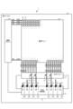
- FIG. 1 is a diagram illustrating an example of a schematic configuration of a display device 1 according to an embodiment. 5 is a diagram showing an example of a schematic configuration of a selector 51.
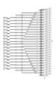
- FIG. 2 is a diagram showing an example of a schematic configuration of a plurality of routes P.
- FIG. 3 is a diagram illustrating an example of a schematic configuration of a connection path CP.
- FIG. 3 is a diagram illustrating an example of a schematic configuration of a connection path CP.
- FIG. 3 is a diagram illustrating an example of a schematic configuration of a dummy route DP.
- FIG. 3 is a diagram illustrating an example of a schematic configuration of a dummy route DP.
- FIG. 3 is a diagram illustrating an example of a schematic configuration of a dummy route DP.
- FIG. 3 is a diagram illustrating an example of a schematic configuration of a dummy route DP.
- FIG. 3 is a diagram illustrating an example of a schematic configuration of a dummy route DP.
- FIG. 3 is a diagram showing an example of specifying a disconnection location.
- 3 is a diagram illustrating an example of current consumption I for each path P.
- FIG. 3 is a flowchart illustrating an example of an analysis method. It is a figure showing a modification. It is a figure showing a modification. It is a figure showing a modification.
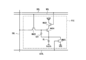
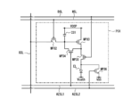
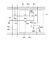
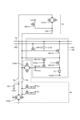
- FIG. 3 is a diagram showing an example of a configuration of a pixel PIX. It is a figure which shows another example of a structure of pixel PIX.
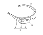
- FIG. 1 is a diagram showing an example of the appearance of a head-mounted display 110.
- FIG. 7 is a diagram illustrating an example of the appearance of another head-mounted display 120.
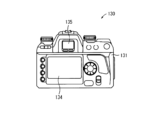
- FIG. 1 is a diagram showing an example of the appearance of a digital still camera 130.
- FIG. 1 is a diagram showing an example of the appearance of a digital still camera 130.
- FIG. 2 is a diagram illustrating an example of the appearance of a television device 140.
- FIG. 2 is a diagram showing an example of the appearance of a smartphone 150.
- FIG. 1 is a diagram showing an example of a configuration of a vehicle to which the technology of the present disclosure is applied.
- FIG. 1 is a diagram showing an example of a configuration of a vehicle to which the technology of the present disclosure is applied.
- Embodiment FIG. 1 is a diagram showing an example of a schematic configuration of a display device 1 according to an embodiment.
- the display device 1 includes a display panel 2, a pixel array 3, a vertical driver 4, a horizontal driver 5, a DDIC 6, and a plurality of paths P.
- the display panel 2 is provided with a pixel array 3, a vertical driver 4, a horizontal driver 5, a DDIC 6, and a plurality of paths P.
- a pixel array 3, a vertical driver 4, a horizontal driver 5, and a plurality of paths P are formed on the display panel 2 by a semiconductor process or the like.
- the DDIC 6 is an example of a control unit in the display device 1, and is manufactured separately from the display panel 2 and mounted on the display panel 2, for example.
- a circuit or the like having the same function as the DDIC 6 may be directly formed on the display panel 2 as a control section. As long as there is no contradiction, the DDIC 6 and the control unit may be read as appropriate. Note that the arrangement of each element on the display panel 2 is not limited to the example shown in FIG. 1.
- the pixel array 3 includes a plurality of pixels 31.
- the plurality of pixels 31 are arranged two-dimensionally in the horizontal and vertical directions.
- One pixel 31 may be a sub-pixel that emits any one of red light (R), green light (G), and blue light (B).
- Each pixel 31 includes, for example, a light emitting element, a transistor, a capacitor, and the like.
- An example of a light emitting device is an OLED.
- Various known pixel configurations may be employed, and some specific examples will be described later with reference to FIGS. 16-23.
- the vertical driver 4 selects and drives the pixels 31 corresponding to the horizontal display line.
- Vertical driver 4 is connected to pixel array 3 via a plurality of control lines WSL.
- one control line WSL is connected to each of the pixels 31 arranged in the horizontal direction.
- the vertical driver 4 selects a control line WSL and supplies a control signal WS for controlling light emission and non-light emission of the corresponding pixel 31 to the selected control line WSL.
- to be connected may be interpreted to mean “to be electrically connected” to the extent that there is no contradiction.
- Electrically connected may be interpreted to include a mode in which other elements are interposed between the connected elements, as long as the functions of the connected elements are not hindered.
- the horizontal driver 5 selects and drives the pixels 31 corresponding to the display line in the vertical direction.
- Horizontal driver 5 is connected to pixel array 3 via a plurality of signal lines SGL.
- one signal line SGL is connected to each of the pixels 31 arranged in the vertical direction.
- the horizontal driver 5 selects a signal line SGL and supplies a pixel signal SG for controlling the amount of light emission (brightness, etc.) of the corresponding pixel 31 to the selected signal line SGL.
- the horizontal driver 5 includes a plurality of selectors 51 provided between the pixel array 3 and the DDIC 6. Each selector 51 connects or disconnects the corresponding output terminal 62 of the DDIC 6 and the corresponding pixel 31 of the pixel array 3. Further details of the selector 51 will be explained later with reference to FIG.
- the DDIC 6 is a display driver IC (Integrated Circuit) that drives the display device 1.
- the DDIC 6 is connected to the vertical driver 4 and the horizontal driver 5, respectively.
- the DDIC 6 supplies the vertical driver 4 with a control signal for controlling the selection of the pixels 31 by the vertical driver 4 and the like.
- the vertical driver 4 supplies a control signal WS to each pixel 31 based on the control signal from the DDIC 6.
- the DDIC 6 supplies the horizontal driver 5 with a control signal for controlling the selection of the pixels 31 by the horizontal driver 5.
- the horizontal driver 5 selects a pixel 31 corresponding to a vertical display line based on a control signal from the DDIC 6.
- the DDIC 6 supplies the video signal FS to the horizontal driver 5.
- the DDIC 6 includes a plurality of output terminals 62 that can output the video signal FS.
- the video signal FS from each output terminal 62 is supplied to the horizontal driver 5.
- the horizontal driver 5 supplies the video signal FS from the DDIC 6 to the selected pixel 31 via the corresponding signal line SGL.
- the video signal FS supplied to the pixel 31 via the signal line SGL is shown as a pixel signal SG.
- the pixel signal SG is a voltage signal (for example, a pulse voltage) that charges a capacitor within the pixel 31. This charging current is supplied from the output terminal 62 of the DDIC 6.
- the multiple routes P include multiple connection routes CP and one or more dummy routes DP.
- the connection path CP of the connection path CP and the dummy path DP connects the output terminal 62 of the DDIC 6 and the selector 51. That is, the selector 51 is connected to the output terminal 62 of the DDIC 6 via the connection path CP. This will be explained with reference to FIG. 2 as well.
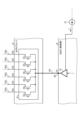
- FIG. 2 is a diagram showing an example of a schematic configuration of the selector 51.
- One selector 51 and its surrounding portion are schematically shown.
- the selector 51 is a demultiplexer configured to receive one video signal FS and output a plurality of pixel signals SG.
- the selector 51 includes a plurality of switches 52 that can be individually controlled on and off.
- the plurality of switches 52 are, for example, field effect transistors (FETs) connected in parallel.
- FETs field effect transistors
- each switch 52 One end of each switch 52 is connected to the same connection path CP. The other end of each switch 52 is connected to a signal line SGL heading toward the corresponding pixel 31 (FIG. 1).
- one selector 51 includes six switches 52, and six corresponding signal lines SGL are connected to pixels 31 forming two display lines.
- the DDIC 6 includes an amplifier 61 corresponding to the selector 51.
- the output terminal of amplifier 61 is connected to output terminal 62 .
- Video signal FS is output via amplifier 61 and output terminal 62.
- the amplifier 61 operates using voltage and current (power) from the power supply 21 provided in the display panel 2 (FIG. 1).
- the power supply 21 is also connected to other parts of the DDIC 6, such as an amplifier other than the illustrated amplifier 61, and supplies the power consumed by the DDIC 6.
- the current flowing from the power supply 21 to the DDIC 6 is referred to as a consumption current I of the DDIC 6 in the drawing.
- the selector 51 as described above is connected to the corresponding output terminal 62 of the DDIC 6 via the connection path CP.
- a plurality of routes P including the connection route CP and the dummy route DP will be explained with reference to FIG. 3.
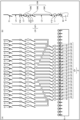
- FIG. 3 is a diagram showing an example of a schematic configuration of a plurality of routes P.
- the multiple routes P include multiple connection routes CP and multiple dummy routes DP.
- One ends of the connection path CP and the dummy path DP are connected to the corresponding output terminals 62 of the DDIC 6.
- connection path CP The other end of the connection path CP is connected to the corresponding selector 51 of the horizontal driver 5.
- the connection path CP is connected between the output terminal 62 and the selector 51 and supplies the video signal FS from the output terminal 62 to the selector 51.
- the other end of the dummy path DP is not connected to any selector 51.
- the dummy path DP is designed such that the current load on the output terminal 62 of the DDIC 6 to which the dummy path DP is connected is smaller than the current load on the output terminal 62 to which the connection path CP is connected.
- the larger the current load the larger the current at the output terminal 62 when outputting the same video signal FS. It can also be said that the larger the current load, the larger the capacity when looking at the path P from the output terminal 62.
- the multiple routes P include multiple dummy routes DP having mutually different lengths.
- Each dummy route DP is shorter than the connection route CP, and the other end of the dummy route DP is open.
- the current load on the output terminal 62 becomes smaller due to reasons such as a smaller wiring capacitance.
- connection path CP and dummy path DP Examples of specific configurations of the connection path CP and dummy path DP will be described with reference to FIGS. 4 to 9.
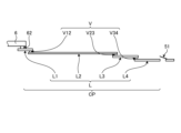
- FIG. 4 and 5 are diagrams showing examples of the schematic configuration of the connection path CP.
- FIG. 4 schematically shows a planar layout of the connection path CP.
- FIG. 5 schematically shows a side layout of the connection path CP.
- the connection path CP includes a plurality of wirings L and one or more vias V.
- the plurality of wiring lines L are connected in series between the output terminal 62 of the DDIC 6 and the selector 51. Adjacent wirings L among the plurality of wirings L are connected via vias V so as to extend through different wiring layers.
- the wiring layer is, for example, a wiring layer of a multilayer substrate that constitutes the display panel 2.
- the wiring L1, the wiring L2, the wiring L3, and the wiring L4 are illustrated as the wiring L.
- the vias V include a via V12, a via V23, and a via V34.
- the wiring L1, the via V12, the wiring L2, the via V23, the wiring L3, the via V34, and the wiring L4 are connected in this order from the output terminal 62 of the DDIC 6 toward the selector 51.
- the wiring L1 is provided on the surface layer of the display panel 2 on which the DDIC 6 is mounted.
- the wiring L2, the wiring L3, and the wiring L4 are provided in the inner layer of the display panel 2.
- the via V12 connects the wiring L1 and the wiring L2.
- Via V23 connects wiring L2 and wiring L3.
- Via V34 connects wiring L3 and wiring L4.
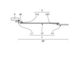
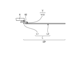
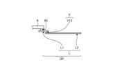
- FIGS. 6 to 9 are diagrams showing examples of the schematic configuration of the dummy route DP. Side layouts of dummy paths DP having different lengths are schematically shown.
- the dummy route DP includes a smaller number of wires L than the plurality of wires L of the connection route CP.
- the wiring L located closest to the selector 51 in the dummy path DP may be shorter than the corresponding wiring L in the connection path CP.
- the dummy path DP differs from the connection path CP (FIG. 5) in that it does not include the wiring L4 and the via V34.
- the dummy path DP also does not include the wiring L3 and the via V23.
- the wiring L2 located closest to the selector 51 in the dummy path DP is the wiring L2, and this wiring L2 is shorter than the wiring L2 (FIG. 5) of the connection path CP.
- the dummy path DP also does not include the wiring L2 and the via V12.
- the defective connection path CP and its defective location can be identified. be able to.
- the defect is a disconnection.
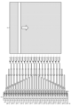
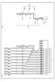
- FIG. 10 is a diagram showing a specific example of a disconnection location.
- connection paths CP-1 to CP18 they are referred to as connection paths CP-1 to CP18 in the drawing.
- dummy route DP-1 to dummy route DP-10 are referred to in the drawing.
- the video signal FS is output so that the current at one output terminal 62 is larger than the current at the other output terminal 62.
- each output terminal 62 of the DDIC 6 outputs the video signal FS so that only the display line (the pixel 31 of the pixel array 3) corresponding to the connection path CP of that one output terminal 62 emits white light.
- the current consumption I (FIG. 2) of the DDIC 6 is measured.
- the video signal FS is output so that the current at another output terminal 62 is larger than the current at the other output terminal 62, and the current consumption I of the DDIC 6 is measured. Similar measurements are made across all output terminals 62. That is, the current consumption I of the DDIC 6 is measured for each of the plurality of paths P corresponding to the plurality of output terminals 62.
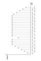
- FIG. 11 is a diagram showing an example of current consumption I for each path P.
- the horizontal axis of the graph indicates the route P.
- the vertical axis of the graph indicates the magnitude of current consumption I.
- the magnitude of the current consumption I of each path P is shown by a circle plot.
- connection path CP in this example, among the connection paths CP-1 to CP-18, only the current consumption I of the connection path CP-5 is smaller. That is, among the plurality of output terminals 62 to which the connection paths CP-1 to CP-18 are connected, only the current load of the output terminal 62 to which the connection path CP-5 is connected is reduced. This means that the capacitance of the connection path CP-5 when viewed from the output terminal 62 is small, that is, the connection path CP-5 is open midway. Therefore, it can be specified that a disconnection has occurred in the connection path CP-5.
- the current consumption I of the dummy path DP-1 to DP-10 is the same as that of the connection path CP-1 to CP-4 and the connection path CP-6 to which no disconnection has occurred. It is smaller than the current consumption I of the connection path CP-10. Furthermore, the magnitude of current consumption I differs for each dummy path DP.
- the magnitude of the current consumption I of the connection path CP-5 is close to the magnitude of the current consumption I of the dummy path DP-4. From this, it can be inferred that the connection path CP-5 is disconnected like the dummy path DP-4. That is, it can be estimated that a disconnection occurs at the position of the connection path CP-5 corresponding to the other end (open end) of the dummy path DP-4. Therefore, that position can be specified as the disconnection point of the connection path CP-5.
- connection path CP in which a disconnection has occurred among the plurality of connection paths CP, and further to specify the disconnection location of the connection path CP.
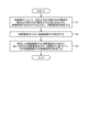
- FIG. 12 is a flowchart showing an example of the analysis method. This analysis method is used, for example, when making a prototype of the display device 1, when analyzing a returned product, etc. The details of each step are as described above, so detailed description will not be repeated.
- step S1 the video signal FS is output for each path P so that the current at the corresponding output terminal 62 is larger than the current at the other output terminals 62.
- the current consumption I of the DDIC 6 is measured.
- the video signal FS as described above with reference to FIG. 10 is output from each output terminal 62 of the DDIC 6.
- a connection path CP with a small current consumption I is identified. For example, as described above with reference to FIG. 11, among the plurality of connection paths CP, a connection path CP having a smaller current consumption I than other connection paths CP is specified.
- step S3 the disconnection location of the specified connection path CP is identified based on the dummy path DP of the current consumption I that is close to the size of the current consumption I of the specified connection path CP. For example, as described above with reference to FIG. 11, the position of the connection path CP corresponding to the open end of the dummy path DP is specified as the disconnection point.
- connection path CP in which a disconnection has occurred among the plurality of connection paths CP, and further to specify the location of the disconnection.
- Identification of the disconnection location can be used for subsequent failure analysis and the like. For example, work such as failure analysis can be performed more efficiently by narrowing down the number of disconnection locations.
- the DDIC 6 may be designed to facilitate the above analysis method.
- the DDIC 6 may be designed so that it can be switched to a dedicated mode (analysis mode) in which the video signal FS corresponding to each path P is output at high speed in step S1.
- a dedicated mode analysis mode
- power consumption other than the output of the video signal FS may be suppressed so that the magnitude of the current of each output terminal 62 of the DDIC 6 is easily reflected in the magnitude of the current consumption I of the DDIC 6.
- FIGS. 13 to 15 are diagrams showing modified examples.
- the connection path CP is also the dummy path DP.
- all of the plurality of connection paths CP also function as dummy paths DP.
- the connection path CP includes switches SW connected in series therein. Examples of the switch SW include a switch SW1, a switch SW2, and a switch SW3. By turning off (non-conducting) one of the switches SW, the connection path CP can function as a dummy path DP that is shorter than the connection path CP. The number of routes P can be reduced.
- connection paths CP may have the configuration shown in FIG. 13(B) described above, and may be used as dummy paths DP.
- the dummy path DP includes switches SW connected in series therein.
- Examples of the switch SW include a switch SW1, a switch SW2, and a switch SW3.
- the position of the corresponding dummy path DP can be opened.
- the length of the dummy path DP connected to the output terminal 62 can be changed by the combination of on/off of each switch SW. That is, one dummy route DP can function as a plurality of dummy routes DP having different lengths. The number of dummy routes DP can be reduced accordingly.
- the dummy path DP includes a capacitor C.
- the other end of the dummy path DP is connected to ground GND via a capacitor C.
- the capacitance of the dummy path DP when viewed from the output terminal 62 increases by the amount that the capacitor C is connected to the dummy path DP.
- the capacitor C is designed to have the same capacitance as the wiring capacitance of the wiring L described above, for example.
- the capacitance of the capacitor C may be different so that the wiring capacitance of each dummy path DP is different. By realizing the wiring capacitance of the dummy path DP with the capacitor C, the dummy path DP can be shortened.
- the defect in the connection path CP may be a short circuit.
- the other end of the dummy path DP may be short-circuited.
- the current consumption I of the connection path CP in which the short circuit has occurred is larger than the current consumption I in the other connection paths CP, and thereby the connection path CP in which the short circuit has occurred is specified.
- the current consumption I of the dummy path DP is larger than the current consumption I of the connection path CP in which no short circuit has occurred, and by comparing with such dummy path DP, the short-circuit location of the connection path CP in which the short circuit has occurred can be identified. Can be done.
- the display device 1 includes the pixel array 3, the DDIC 6 (an example of a control unit), a plurality of selectors 51, and a plurality of paths P.
- Pixel array 3 includes a plurality of pixels 31.
- DDIC 6 includes a plurality of output terminals 62 that output video signals FS.
- Each of the plurality of selectors 51 is provided between the pixel array 3 and the DDIC 6 so as to electrically connect or electrically disconnect the corresponding output terminal 62 of the DDIC 6 and the corresponding pixel 31 of the pixel array 3. .
- each of the plurality of paths P is connected to the corresponding output terminal 62.
- the plurality of paths P include a plurality of connection paths CP whose respective other ends are connected to the corresponding selectors 51, and dummy paths DP whose respective other ends are not connected to the corresponding selectors 51. According to such a display device 1, for example, as described above with reference to FIGS. 10 to 12, it is possible to identify a defective location in the connection path CP between the output terminal 62 of the DDIC 6 and the switch 52. Can be done.
- the dummy route DP may be shorter than the connection route CP.
- the plurality of routes P may include a plurality of dummy routes DP having mutually different lengths.
- the connection path CP includes a plurality of wires L connected in series between the output terminal 62 and the selector 51, and the dummy path DP includes a smaller number of wires L than the plurality of wires L of the connection path CP. may be included.
- Adjacent wirings L among the plurality of wirings L may be connected via vias V so as to extend through different wiring layers.
- the wiring L located closest to the selector 51 in the dummy path DP may be shorter than the corresponding wiring L in the connection path CP.
- the other end of the dummy path DP may be open. For example, by using such a dummy route DP, it is possible to specify a disconnection point in the connection route CP.
- connection paths CP include switches SW connected in series in the connection paths CP, and at least some of the connections
- the route CP may also be a dummy route DP. Thereby, the number of routes P can be reduced.
- the dummy path DP may include switches SW connected in series therein. Thereby, one dummy route DP can function as a plurality of dummy routes DP having mutually different lengths. The number of dummy routes DP can be reduced accordingly.
- the other end of the dummy path DP may be connected to the ground GND via the capacitor C.
- the dummy path DP can be shortened.
- the analysis method described with reference to FIGS. 10 to 12 and the like is also one of the techniques disclosed.
- the analysis method is an analysis method for the display device 1 having the configuration described so far, and is based on the assumption that the current load of each output terminal 62 is the same for each of the plurality of paths P.
- the video signal FS is output so that the current of the output terminal 62 is larger than the current of the other output terminals 62, and the current consumption I of the DDIC 6 is measured (step S1). Based on the measurement results, multiple connection paths are output. This includes identifying a defective location in at least one connection path CP among the CPs (steps S2 to S3).
- identifying means identifying a connection path CP with a small current consumption I based on the measurement results (step S2), and identifying a connection path CP with a small consumption current I of the specified connection path CP.
- This includes identifying a disconnection point in the connection path CP based on the dummy path DP of the current I (step S3).
- FIGS. 16 to 23 Several examples of pixel circuits will be described with reference to FIGS. 16 to 23. In addition, in those figures, a pixel is shown as pixel PIX.
- FIG. 16 is a diagram showing an example of the configuration of pixel PIX.
- Pixel PIX includes a capacitor C01, transistors MN02 to MN03, and a light emitting element EL.
- the transistors MN02 to MN03 are N-type MOSFETs (Metal Oxide Semiconductor Field Effect Transistors).
- the gate of the transistor MN02 is connected to the control line WSL, the drain is connected to the signal line SGL, and the source is connected to the gate of the transistor MN03 and the capacitor C01.
- One end of the capacitor C01 is connected to the source of the transistor MN02 and the gate of the transistor MN03, and the other end is connected to the source of the transistor MN03 and the anode of the light emitting element EL.
- the gate of the transistor MN03 is connected to the source of the transistor MN02 and one end of the capacitor C01, the drain is connected to the power supply line VCCP, and the source is connected to the other end of the capacitor C01 and the anode of the light emitting element EL.
- the light emitting element EL is, for example, an organic EL light emitting element, and has an anode connected to the source of the transistor MN03 and the other end of the capacitor C01, and a cathode connected to the power supply line Vcath.
- the pixel PIX when the transistor MN02 is turned on, the voltage across the capacitor C01 is set based on the pixel signal supplied from the signal line SGL.
- Transistor MN03 causes a current corresponding to the voltage across capacitor C01 to flow through light emitting element EL.
- the light emitting element EL emits light based on the current supplied from the transistor MN03. In this way, the pixel PIX emits light with a brightness according to the pixel signal.
- FIG. 17 is a diagram showing another example of the configuration of the pixel PIX.
- This pixel PIX includes capacitors C11 and C12, transistors MP12 to MP15, and a light emitting element EL.
- Transistors MP12 to MP15 are P-type MOSFETs.
- the gate of the transistor MP12 is connected to the control line WSL, the source is connected to the signal line SGL, and the drain is connected to the gate of the transistor MP14 and the capacitor C12.
- One end of the capacitor C11 is connected to the power supply line VCCP, and the other end is connected to the capacitor C12, the drain of the transistor MP13, and the source of the transistor MP14.
- One end of the capacitor C12 is connected to the other end of the capacitor C11, the drain of the transistor MP13, and the source of the transistor MP14, and the other end is connected to the drain of the transistor MP12 and the gate of the transistor MP14.
- the gate of the transistor MP13 is connected to the control line DSL, the source is connected to the power supply line VCCP, and the drain is connected to the source of the transistor MP14, the other end of the capacitor C11, and one end of the capacitor C12.
- the gate of the transistor MP14 is connected to the drain of the transistor MP12 and the other end of the capacitor C12, the source is connected to the drain of the transistor MP13, the other end of the capacitor C11, and one end of the capacitor C12, and the drain is connected to the anode of the light emitting element EL and the other end of the capacitor C12. Connected to the source of MP15.
- the gate of the transistor MP15 is connected to the control line AZSL, the source is connected to the drain of the transistor MP14 and the anode of the light emitting element EL, and the drain is connected to the power supply line VSS.
- the transistor MP12 when the transistor MP12 is turned on, the voltage across the capacitor C12 is set based on the pixel signal supplied from the signal line SGL.
- Transistor MP13 is turned on and off based on a signal on control line DSL.
- the transistor MP14 causes a current corresponding to the voltage across the capacitor C12 to flow through the light emitting element EL during the period when the transistor MP13 is in the on state.
- the light emitting element EL emits light based on the current supplied from the transistor MP14. In this way, the pixel PIX emits light with a brightness according to the pixel signal.
- Transistor MP15 is turned on and off based on a signal on control line AZSL. During the period when the transistor MP15 is in the on state, the voltage of the anode of the light emitting element EL is initialized by being set to the voltage of the power supply line VSS.
- FIG. 18 is a diagram showing another example of the configuration of the pixel PIX.
- This pixel PIX includes a capacitor C21, transistors MN22 to MN25, and a light emitting element EL.
- Transistors MN22 to MN25 are N-type MOSFETs.
- the gate of the transistor MN22 is connected to the control line WSL, the drain is connected to the signal line SGL, and the source is connected to the gate of the transistor MN24 and the capacitor C21.
- One end of the capacitor C21 is connected to the source of the transistor MN22 and the gate of the transistor MN24, and the other end is connected to the source of the transistor MN24, the drain of the transistor MN25, and the anode of the light emitting element EL.
- the gate of the transistor MN23 is connected to the control line DSL, the drain is connected to the power supply line VCCP, and the source is connected to the drain of the transistor MN24.
- the gate of the transistor MN24 is connected to the source of the transistor MN22 and one end of the capacitor C21, the drain is connected to the source of the transistor MN23, and the source is connected to the other end of the capacitor C21, the drain of the transistor MN25, and the anode of the light emitting element EL. Ru.
- the gate of the transistor MN25 is connected to the control line AZSL, the drain is connected to the source of the transistor MN24, the other end of the capacitor C21, and the anode of the light emitting element EL, and the source is connected to the power supply line VSS.
- the transistor MN22 when the transistor MN22 is turned on, the voltage across the capacitor C21 is set based on the pixel signal supplied from the signal line SGL.
- the transistor MN23 is turned on and off based on the signal on the control line DSL.
- the transistor MN24 causes a current corresponding to the voltage across the capacitor C21 to flow through the light emitting element EL during the period when the transistor MN23 is in the on state.
- the light emitting element EL emits light based on the current supplied from the transistor MN24. In this way, the pixel PIX emits light with a brightness according to the pixel signal.
- Transistor MN25 is turned on and off based on a signal on control line AZSL. During the period when the transistor MN25 is in the on state, the voltage of the anode of the light emitting element EL is initialized by being set to the voltage of the power supply line VSS.
- FIG. 19 is a diagram showing another example of the configuration of the pixel PIX.
- This pixel PIX includes a capacitor C31, transistors MP32 to MP36, and a light emitting element EL.
- Transistors MP32 to MP36 are P-type MOSFETs.
- the gate of the transistor MP32 is connected to the control line WSL, the source is connected to the signal line SGL, and the drain is connected to the gate of the transistor MP33, the drain of the transistor MP34, and the capacitor C31.
- One end of the capacitor C31 is connected to the power supply line VCCP, and the other end is connected to the drain of the transistor MP32, the gate of the transistor MP33, and the drain of the transistor MP34.
- the gate of the transistor MP34 is connected to the control line AZSL1, the source is connected to the drain of the transistor MP33 and the source of the transistor MP35, and the drain is connected to the drain of the transistor MP32, the gate of the transistor MP33, and the other end of the capacitor C31.
- the gate of the transistor MP35 is connected to the control line DSL, the source is connected to the drain of the transistor MP33 and the source of the transistor MP34, and the drain is connected to the source of the transistor MP36 and the anode of the light emitting element EL.
- the gate of the transistor MP36 is connected to the control line AZSL2, the source is connected to the drain of the transistor MP35 and the anode of the light emitting element EL, and the drain is connected to the power supply line VSS.
- the transistor MP32 when the transistor MP32 is turned on, the voltage across the capacitor C31 is set based on the pixel signal supplied from the signal line SGL.
- Transistor MP35 is turned on and off based on a signal on control line DSL.
- the transistor MP33 causes a current corresponding to the voltage across the capacitor C31 to flow through the light emitting element EL during the period when the transistor MP35 is in the on state.
- the light emitting element EL emits light based on the current supplied from the transistor MP33. In this way, the pixel PIX emits light with a brightness according to the pixel signal.
- Transistor MP34 is turned on and off based on the signal on control line AZSL1.
- Transistor MP36 is turned on and off based on the signal on control line AZSL2.
- the voltage of the anode of the light emitting element EL is initialized by being set to the voltage of the power supply line VSS.
- FIG. 20 is a diagram showing another example of the configuration of the pixel PIX.
- One end of the capacitor C48 is connected to the signal line SGL1, and the other end is connected to the power supply line VSS.
- One end of the capacitor C49 is connected to the signal line SGL1, and the other end is connected to the signal line SGL2.
- the transistor MP49 is a P-type MOSFET, and has a gate connected to the control line WSL2, a source connected to the signal line SGL1, and a drain connected to the signal line SGL2.
- Pixel PIX includes a capacitor C41, transistors MP42 to MP46, and a light emitting element EL.
- Transistors MP42 to MP46 are P-type MOSFETs.
- the gate of the transistor MP42 is connected to the control line WSL1, the source is connected to the signal line SGL2, and the drain is connected to the gate of the transistor MP43 and the capacitor C41.
- One end of the capacitor 41 is connected to the power supply line VCCP, and the other end is connected to the drain of the transistor MP42 and the gate of the transistor MP43.
- the gate of the transistor MP43 is connected to the drain of the transistor MP42 and the other end of the capacitor C41, the source is connected to the power supply line VCCP, and the drain is connected to the sources of the transistors MP44 and MP45.
- the gate of the transistor MP44 is connected to the control line AZSL1, the source is connected to the drain of the transistor MP43 and the source of the transistor MP45, and the drain is connected to the signal line SGL2.
- the gate of the transistor MP45 is connected to the control line DSL, the source is connected to the drain of the transistor MP43 and the source of the transistor MP44, and the drain is connected to the source of the transistor MP46 and the anode of the light emitting element EL.
- the gate of the transistor MP46 is connected to the control line AZSL2, the source is connected to the drain of the transistor MP45 and the anode of the light emitting element EL, and the drain is connected to the power supply line VSS.
- the transistor MP42 when the transistor MP42 is turned on, the voltage across the capacitor C41 is set based on the pixel signal supplied from the signal line SGL1 via the capacitor C49.
- Transistor MP45 is turned on and off based on a signal on control line DSL.
- the transistor MP43 causes a current corresponding to the voltage across the capacitor C41 to flow through the light emitting element EL during the period when the transistor MP45 is in the on state.
- the light emitting element EL emits light based on the current supplied from the transistor MP43. In this way, the pixel PIX emits light with a brightness according to the pixel signal.
- Transistor MP44 is turned on and off based on the signal on control line AZSL1.
- Transistor MP46 is turned on and off based on the signal on control line AZSL2.
- the voltage of the anode of the light emitting element EL is initialized by being set to the voltage of the power supply line VSS.
- FIG. 21 is a diagram showing another example of the configuration of the pixel PIX.
- the plurality of pixels PIX are provided in a matrix in the display area 100, and the display area 100 is provided between the first control section 40 and the second control section 70.
- the first control section 40 includes transmission gates TG45 and TG46, transistors MP56 and MP57, and a capacitor C61.
- Transistors MP56 and MP57 are P-type MOSFETs.
- a pixel signal is supplied to the input end of the transmission gate TG45, and the output end of the transmission gate TG45 is connected to one end of the signal line 14a.
- the input end of transmission gate TG46 is connected to signal line 14b, and the output end of transmission gate TG46 is connected to power supply line Vorst.
- One end of the capacitor C61 is connected to the signal line 14a, and the other end is connected to the power supply line VSS1.
- the gate of the transistor MP56 is connected to the control line, the source is connected to the power supply line Vini, and the drain is connected to the signal line 14b.
- the gate of the transistor MP57 is connected to the control line, the source is connected to the power supply line Vel, and the drain is connected to the signal line 14b.
- the second control section 70 includes a transmission gate TG72, a transistor MP73, and a capacitor C82.
- Transistor MP73 is a P-type MOSFET.
- the input end of the transmission gate TG72 is connected to the other end of the signal line 14a, and the output end is connected to the drain of the transistor MP73 and one end of the capacitor C82.
- the gate of transistor MP73 is connected to the control line, the source is connected to power supply line Vref, and the drain is connected to the output terminal of transmission gate MP72 and one end of capacitor C82.
- One end of the capacitor C82 is connected to the output end of the transmission gate TG72 and the drain of the transistor MP73, and the other end is connected to one end of the signal line 14b.
- Pixel PIX includes a capacitor C132, transistors MP121 to MP125, and a light emitting element EL.
- Transistors MP121 to MP125 are P-type MOSFETs.
- the gate of the transistor MP122 is connected to the control line WSL, the source is connected to the signal line 14b, and the drain is connected to the gate of the transistor MP121 and the capacitor C132.
- One end of the capacitor C132 is connected to the power supply line Vel, and the other end is connected to the drain of the transistor MP122 and the gate of the transistor MP121.
- the gate of the transistor MP121 is connected to the drain of the transistor MP122 and the other end of the capacitor C132, the source is connected to the power supply line Vel, and the drain is connected to the sources of the transistors MP123 and MP124.
- the gate of the transistor MP123 is connected to the control line AZSL, the source is connected to the drain of the transistor MP121 and the source of the transistor MP124, and the drain is connected to the signal line 14b.
- the gate of the transistor MP124 is connected to the control line, the source is connected to the drain of the transistor MP121 and the source of the transistor MP123, and the drain is connected to the drain of the transistor MP125 and the anode of the light emitting element EL.
- the gate of the transistor MP125 is connected to the control line AZSL, the source is connected to the power supply line Vorst, and the drain is connected to the drain of the transistor MP124 and the anode of the light emitting element EL.
- the capacitor C132 is turned on based on the pixel signal supplied via the transmission gate TG45, the signal line 14a, the transmission gate TG72, the capacitor C82, and the signal line 14b.
- the voltage across is set.
- Transistor MP124 is turned on and off based on a signal on the control line.
- the transistor MP121 causes a current corresponding to the voltage across the capacitor C132 to flow through the light emitting element EL during the period when the transistor MP124 is in the on state.
- the light emitting element EL emits light based on the current supplied from the transistor MP121. In this way, the pixel PIX emits light with a brightness according to the pixel signal.
- Transistors MP123 and MP125 are turned on and off based on the signal on the control line AZSL. During the period when the transistor MP123 is on, the drain of the transistor MP121 and the source of the transistor MP124 are connected to the signal line 14b. During the period in which the transistor MP125 is in the on state, the voltage of the anode of the light emitting element EL is initialized by being set to the voltage of the power supply line Vorst. Further, the transistor MP56 is turned on and off based on the signal on the control line, the transistor MP57 is turned on and off based on the signal on the control line, and the transistor MP73 is turned on and off based on the signal on the control line.
- the signal line 14b When the transistor MP56 is turned on, the signal line 14b is set to the voltage of the power line Vini, and when the transistor MP57 is turned on, the signal line 14b is set to the voltage of the power line Vel.
- transistor MP73 When transistor MP73 is turned on, one end of capacitor C82 is initialized by being set to the voltage of power supply line Vref.
- FIG. 22 is a diagram showing another example of the configuration of the pixel PIX.
- This pixel PIX includes a capacitor C51, transistors MP52 to MP60, and a light emitting element EL.
- Transistors MP52 to MP60 are P-type MOSFETs.
- the gate of the transistor MP52 is connected to the control line WSL, the source is connected to the signal line SGL, and the drain is connected to the drain of the transistor MP53 and the source of the transistor MP54.
- the gate of the transistor MP53 is connected to the control line DSL, the source is connected to the power supply line VCCP, and the drain is connected to the drain of the transistor MP52 and the source of the transistor MP54.
- the gate of transistor MP54 is connected to the source of transistor MP55, the drain of transistor MP57, and capacitor C51, the source is connected to the drains of transistors MP52 and MP53, and the drain is connected to the sources of transistors MP58 and MP59.
- One end of the capacitor C51 is connected to the power supply line VCCP, and the other end is connected to the gate of the transistor MP54, the source of the transistor MP55, and the drain of the transistor MP57.
- Capacitor C51 may include two capacitors connected in parallel.
- the gate of the transistor MP55 is connected to the control line AZSL1, the source is connected to the gate of the transistor MP54, the drain of the transistor MP57, and the other end of the capacitor C51, and the drain is connected to the source of the transistor MP56.
- the gate of transistor MP56 is connected to control line AZSL1, the source is connected to the drain of transistor MP55, and the drain is connected to power supply line VSS.
- the gate of transistor MP57 is connected to control line WSL, the drain is connected to the gate of transistor MP54, the source of transistor MP55, and the other end of capacitor C51, and the source is connected to the drain of transistor MP58.
- the gate of transistor MP58 is connected to control line WSL, the drain is connected to the source of transistor MP57, and the source is connected to the drain of transistor MP54 and the source of transistor MP59.
- the gate of the transistor 59 is connected to the control line DSL, the source is connected to the drain of the transistor MP54 and the source of the transistor MP58, and the drain is connected to the source of the transistor MP60 and the anode of the light emitting element EL.
- the gate of the transistor MP60 is connected to the control line AZSL2, the source is connected to the drain of the transistor MP59 and the anode of the light emitting element EL, and the drain is connected to the power supply line VSS.
- the voltage across the capacitor C51 is set based on the pixel signal supplied from the signal line SGL by turning on the transistors MP52, MP54, MP58, and MP57.
- Transistors MP53 and MP59 are turned on and off based on the signal on the control line DSL.
- the transistor MP54 causes a current corresponding to the voltage across the capacitor C51 to flow through the light emitting element EL during a period when the transistors MP53 and MP59 are in the on state.
- the light emitting element EL emits light based on the current supplied from the transistor MP54. In this way, the pixel PIX emits light with a brightness according to the pixel signal.
- Transistors MP55 and MP56 are turned on and off based on the signal on the control line AZSL1. During the period when transistors MP55 and MP56 are on, the voltage at the gate of transistor MP54 is initialized by being set to the voltage of power supply line VSS. Transistor MP60 is turned on and off based on the signal on control line AZSL2. During the period when the transistor MP60 is in the on state, the voltage of the anode of the light emitting element EL is initialized by being set to the voltage of the power supply line VSS.
- FIG. 23 is a diagram showing another example of the configuration of the pixel PIX.
- the signal on the control line WSNL and the signal on the control line WSPL are mutually inverted signals.
- Pixel PIX includes capacitors C61 and C62, transistors MN63, MP64, MN65 to MN67, and a light emitting element EL.
- Transistors MN63, MN65 to MN67 are N-type MOSFETs
- transistor MP64 is a P-type MOSFET.
- the gate of the transistor MN63 is connected to the control line WSNL, the drain is connected to the signal line SGL and the source of the transistor MP64, and the source is connected to the drain of the transistor MP64, the capacitors C61 and C62, and the gate of the transistor MN65.
- the gate of the transistor MP64 is connected to the control line WSPL, the source is connected to the signal line SGL and the drain of the transistor MN63, and the drain is connected to the source of the transistor MN63, capacitors C61 and C62, and the gate of the transistor MN65.
- the capacitor C61 is configured using, for example, a MOM (Metal Oxide Metal) capacitor, and one end is connected to the source of the transistor MN63, the drain of the transistor MP64, the capacitor C62, and the gate of the transistor MN65, and the other end is connected to the power supply line VSS2. be done.
- the capacitor C61 may be configured using, for example, a MOS capacitor or an MIM (Metal Insulator Metal) capacitor.
- the capacitor C62 is configured using, for example, a MOS capacitor, and one end is connected to the source of the transistor MN63, the drain of the transistor MP64, one end of the capacitor C61, and the gate of the transistor MN65, and the other end is connected to the power supply line VSS2.
- the capacitor C62 may be configured using, for example, a MOM capacitor or an MIM capacitor.
- the gate of the transistor MN65 is connected to the source of the transistor MN63, the drain of the transistor MP64, and one ends of the capacitors C61 and C62, the drain is connected to the power supply line VCCP, and the source is connected to the drains of the transistors MN66 and MN67.
- the gate of the transistor MN66 is connected to the control line AZL, the drain is connected to the source of the transistor MN65 and the drain of the transistor MN67, and the source is connected to the power supply line VSS1.
- the gate of the transistor MN67 is connected to the control line DSL, the drain is connected to the source of the transistor MN65 and the drain of the transistor MN66, and the source is connected to the anode of the light emitting element EL.
- the pixel PIX when at least one of the transistors MN63 and MP64 is turned on, the voltage across the capacitors C61 and C62 is set based on the pixel signal supplied from the signal line SGL. .
- Transistor MN67 is turned on and off based on a signal on control line DSL.
- the transistor MN65 causes a current corresponding to the voltage across the capacitors C61 and C62 to flow through the light emitting element EL during the period when the transistor MN67 is in the on state.
- the light emitting element EL emits light based on the current supplied from the transistor MP65. In this way, the pixel PIX emits light with a brightness according to the pixel signal.
- Transistor MN66 may be turned on or off based on a signal on control line AZL. Further, the transistor MN66 may function as a resistance element having a resistance value depending on the signal on the control line AZL. In this case, transistor MN65 and transistor MN66 constitute a so-called source follower circuit.
- FIG. 24 is a diagram showing an example of the appearance of the head mounted display 110.
- the head-mounted display 110 has, for example, ear hook parts 112 on both sides of a glasses-shaped display part 111 to be worn on the user's head.
- the techniques related to the above embodiments and the like can be applied to such a head mounted display 110.
- FIG. 25 is a diagram showing an example of the appearance of another head-mounted display 120.
- the head-mounted display 120 is a transmissive head-mounted display that includes a main body part 121, an arm part 122, and a lens barrel part 123.
- This head mounted display 120 is attached to glasses 128.
- the main body section 121 includes a control board and a display section for controlling the operation of the head mounted display 120.
- This display section emits image light of a displayed image.
- the arm portion 122 connects the main body portion 121 and the lens barrel portion 123 and supports the lens barrel portion 123.
- the lens barrel section 123 projects the image light supplied from the main body section 121 via the arm section 122 toward the user's eyes via the lens 129 of the glasses 128 .
- the techniques related to the above embodiments and the like can be applied to such a head-mounted display 120.
- the head mounted display 120 is a so-called light guide plate type head mounted display, but is not limited thereto, and may be, for example, a so-called birdbath type head mounted display.
- This birdbath type head-mounted display includes, for example, a beam splitter and a partially transparent mirror.
- the beam splitter outputs light encoded with image information toward a mirror, which reflects the light toward the user's eyes.
- Both the beam splitter and the partially transparent mirror are partially transparent. This allows light from the surrounding environment to reach the user's eyes.
- FIG. 26 and 27 are diagrams showing an example of the appearance of the digital still camera 130.
- FIG. 26 shows a front view
- FIG. 27 shows a rear view.
- This digital still camera 130 is a single-lens reflex type camera with interchangeable lenses, and includes a camera body 131, a photographing lens unit 132, a grip 133, a monitor 134, and an electronic viewfinder 135.
- the imaging lens unit 312 is an exchangeable lens unit, and is provided near the center of the front of the camera body 311 .
- the grip section 133 is provided on the left side of the front of the camera body section 311, and is designed to be held by the photographer.
- the monitor 134 is provided on the left side of the rear surface of the camera body 131 from approximately the center.
- the electronic viewfinder 135 is provided above the monitor 14 on the back side of the camera body section 131. By looking through the electronic viewfinder 135, the photographer can visually recognize the light image of the subject guided from the photographic lens unit 132 and determine the composition.
- the technology related to the above embodiments and the like can be applied to the electronic viewfinder 135.
- FIG. 28 is a diagram showing an example of the appearance of the television device 140.
- the television device 140 has a video display screen section 141 that includes a front panel 142 and a filter glass 143.
- the techniques related to the above embodiments and the like can be applied to this video display screen section 141.
- FIG. 29 is a diagram showing an example of the appearance of the smartphone 150.
- the smartphone 150 includes a display section 151 that displays various information, and an operation section 152 that includes buttons and the like that accept operation inputs from the user.
- the technology according to the embodiments described above can be applied to this display section 151.
- FIG. 30 and 31 are diagrams illustrating an example of a configuration of a vehicle to which the technology of the present disclosure is applied.
- FIG. 30 shows an example of the interior of the vehicle as seen from the rear of the vehicle
- FIG. 31 shows an example of the interior of the vehicle as seen from the left rear of the vehicle.
- the vehicle in FIGS. 30 and 31 includes a center display 201, a console display 202, a head-up display 203, a digital rear mirror 204, a steering wheel display 205, and a rear entertainment display 106.
- the center display 201 is arranged on the dashboard 261 at a location facing the driver's seat 262 and the passenger seat 263.
- Center display 201 can display information detected by various sensors.
- the center display 201 displays images taken by an image sensor, distance images to obstacles in front of the vehicle and on the sides measured by a ToF sensor, body temperature of the occupant detected by an infrared sensor, etc. can be displayed.
- the center display 201 can be used, for example, to display at least one of safety-related information, operation-related information, life log, health-related information, authentication/identification-related information, and entertainment-related information.
- the safety-related information is based on sensor detection results, such as detection of falling asleep, detection of looking away, detection of mischief by children in the same vehicle, presence or absence of seatbelts, and detection of occupants being left behind.
- the operation-related information is information on gestures related to the occupant's operations, which are detected using a sensor.
- the gesture may include the operation of various equipment in the vehicle, and includes, for example, the operation of an air conditioner, a navigation device, an AV (Audio/Visual) device, a lighting device, and the like.
- the life log includes life logs of all crew members. For example, a life log includes a record of each occupant's actions.
- the health-related information includes information about the occupant's body temperature detected using a temperature sensor and the occupant's health condition estimated based on the detected body temperature.
- information on the occupant's health condition may be estimated based on the occupant's face imaged by an image sensor.
- information regarding the health condition of the occupant may be estimated based on the occupant's response obtained by having a conversation with the occupant using an automated voice.
- Authentication/identification related information includes information such as a keyless entry function that performs facial recognition using a sensor, and a function that automatically adjusts seat height and position using facial recognition.
- the entertainment-related information includes information on the operation of the AV device by the occupant detected by the sensor, information on content to be displayed suitable for the occupant detected and recognized by the sensor, and the like.
- the console display 202 can be used, for example, to display life log information.
- Console display 202 is arranged near shift lever 265 on center console 264 between driver's seat 262 and passenger seat 263.
- Console display 202 can also display information sensed by various sensors. Further, the console display 202 may display an image around the vehicle captured by an image sensor, or may display a distance image to an obstacle around the vehicle.
- the head-up display 203 is virtually displayed behind the windshield 266 in front of the driver's seat 262.
- the head-up display 203 can be used, for example, to display at least one of safety-related information, operation-related information, life log, health-related information, authentication/identification-related information, and entertainment-related information. Since the head-up display 203 is often placed virtually in front of the driver's seat 262, it is difficult to display information directly related to vehicle operation, such as vehicle speed, remaining fuel level, and remaining battery level. suitable for
- the digital rear mirror 204 can not only display the rear of the vehicle but also display the state of the occupants in the rear seats, so it can be used, for example, to display life log information of the occupants in the rear seats.
- the steering wheel display 205 is placed near the center of the steering wheel 267 of the vehicle.
- Steering wheel display 205 can be used, for example, to display at least one of safety-related information, operation-related information, lifelog, health-related information, authentication/identification-related information, and entertainment-related information.
- life log information such as the driver's body temperature, and information regarding the operation of AV equipment, air conditioning equipment, etc. There is.
- the rear entertainment display 206 is attached to the back side of the driver's seat 262 and passenger seat 263, and is for viewing by passengers in the rear seats.
- Rear entertainment display 206 can be used, for example, to display at least one of safety-related information, operation-related information, lifelog, health-related information, authentication/identification-related information, and entertainment-related information.
- the rear entertainment display 206 since the rear entertainment display 206 is located in front of the rear seat occupant, information relevant to the rear seat occupant is displayed.
- the rear entertainment display 206 may display information regarding the operation of the AV device or air conditioning equipment, or may display the results of measuring the body temperature of the passenger in the rear seat using a temperature sensor.
- the technology according to the above embodiments can be applied to the center display 201, console display 202, head-up display 203, digital rear mirror 204, steering wheel display 205, and rear entertainment display 206.
- the present technology can also have the following configuration.
- a pixel array including a plurality of pixels; a control unit including a plurality of output terminals that output video signals; a plurality of selectors provided between the pixel array and the control section, each of which electrically connects or electrically disconnects a corresponding output terminal of the control section and a corresponding pixel of the pixel array; and, a plurality of paths each having one end connected to the corresponding output terminal; Equipped with The plurality of routes are a plurality of connection paths, each other end of which is connected to the corresponding selector; a dummy path whose other end is not connected to the corresponding selector; including, Display device.
- the dummy route is shorter than the connection route;
- the plurality of routes include the plurality of dummy routes having mutually different lengths, The display device according to (1) or (2).
- the connection path includes a plurality of wires connected in series between the output terminal and the selector, the dummy route includes a smaller number of wires than the plurality of wires in the connection route;
- Adjacent wirings among the plurality of wirings are connected via vias so as to extend through different wiring layers;
- a wire located closest to the selector in the dummy route is shorter than a corresponding wire in the connection route.
- At least some of the plurality of connection paths include switches connected in series in the connection path, at least some of the connection paths are also the dummy paths;
- the dummy path includes a switch connected in series in the dummy path.
- the other end of the dummy path is connected to ground via a capacitor.
- a method for analyzing a display device comprising: The display device includes: a pixel array including a plurality of pixels; a control unit including a plurality of output terminals that output video signals; a plurality of selectors provided between the pixel array and the control section, each of which electrically connects or electrically disconnects a corresponding output terminal of the control section and a corresponding pixel of the pixel array; and, a plurality of paths each having one end connected to the corresponding output terminal; Equipped with The plurality of routes are a plurality of connection paths, each other end of which is connected to the corresponding selector; a dummy path whose other end is not connected to the corresponding selector; including; The analysis method is For each of the plurality of paths, when it is assumed that the current load on each output terminal is the same, the video signal is outputted so that the current of the corresponding output terminal is larger than the current of the other output terminals, and , measuring current consumption of the control unit; identifying a defective location in
- Display device 2 Display panel 21 Power source 3 Pixel array 31 Pixel 4 Vertical driver 5 Horizontal driver 51 Selector 52 Switch 6 DDIC (control unit) 61 Amplifier 62 Output terminal P Path CP Connection path DP Dummy path L Wiring SG Pixel signal SGL Signal line SW Switch V Via WS Control signal WSL Control line
Landscapes
- Engineering & Computer Science (AREA)
- Physics & Mathematics (AREA)
- General Physics & Mathematics (AREA)
- Theoretical Computer Science (AREA)
- Computer Hardware Design (AREA)
- Control Of Indicators Other Than Cathode Ray Tubes (AREA)
Abstract
Description
1.実施形態
2.変形例
3.効果の例
4.画素回路の例
5.ユースケースの例
図1は、実施形態に係る表示装置1の概略構成の例を示す図である。表示装置1は、表示パネル2と、画素アレイ3と、垂直ドライバ4と、水平ドライバ5と、DDIC6と、複数の経路Pとを含む。
ダミー経路DPを含む複数の経路Pの構成は、上記の実施形態に限定されない。いくつかの変形例について述べる。
以上で説明した技術は、例えば次のように特定される。開示される技術の1つは、表示装置1である。図1及び図3等を参照して説明したように、表示装置1は、画素アレイ3と、DDIC6(制御部の一例)と、複数のセレクタ51と、複数の経路Pと、を備える。画素アレイ3は、複数の画素31を含む。DDIC6は、映像信号FSを出力する複数の出力端子62を含む。複数のセレクタ51の各々は、DDIC6の対応する出力端子62と画素アレイ3の対応する画素31とを電気的に接続し又は電気的に切り離すように、画素アレイ3とDDIC6との間に設けられる。複数の経路Pの各々は、一端が対応する出力端子62に接続される。複数の経路Pは、各々の他端が対応するセレクタ51に接続された複数の接続経路CPと、各々の他端が対応するセレクタ51に接続されていないダミー経路DPと、を含む。このような表示装置1によれば、例えば先に図10~図12等を参照して説明したように、DDIC6の出力端子62とスイッチ52との間の接続経路CPの欠陥箇所を特定することができる。
画素回路のいくつかの例について、図16~図23を参照して説明する。なお、それらの図では、画素は、画素PIXとして示される。
表示装置1のいくつかのユースケース(適用)の例について、図24~図31を参照して説明する。
図24は、ヘッドマウントディスプレイ110の外観の一例を示す図である。ヘッドマウントディスプレイ110は、例えば、眼鏡形の表示部111の両側に、使用者の頭部に装着するための耳掛け部112を有する。このようなヘッドマウントディスプレイ110に、上記実施の形態等に係る技術を適用することができる。
図25は、他のヘッドマウントディスプレイ120の外観の一例を示す図である。ヘッドマウントディスプレイ120は、本体部121と、アーム部122と、鏡筒部123とを有する、透過式のヘッドマウントディスプレイである。このヘッドマウントディスプレイ120は、眼鏡128に装着されている。本体部121は、ヘッドマウントディスプレイ120の動作を制御するための制御基板や表示部を有している。この表示部は、表示画像の画像光を射出する。アーム部122は、本体部121と鏡筒部123とを連結し、鏡筒部123を支持する。鏡筒部123は、本体部121からアーム部122を介して供給された画像光を、眼鏡128のレンズ129を介して、ユーザの目に向かって投射する。このようなヘッドマウントディスプレイ120に、上記実施の形態等に係る技術を適用することができる。
図26及び図27は、デジタルスチルカメラ130の外観の一例を示す図である。図26は正面図を示し、図27は背面図を示す。このデジタルスチルカメラ130は、レンズ交換式一眼レフレックスタイプのカメラであり、カメラ本体部(カメラボディ)131と、撮影レンズユニット132と、グリップ部133と、モニタ134と、電子ビューファインダ135とを有する。撮像レンズユニット312は、交換式のレンズユニットであり、カメラ本体部311の正面のほぼ中央付近に設けられる。グリップ部133は、カメラ本体部311の正面の左側に設けられ、撮影者は、このグリップ部133を把持するようになっている。モニタ134は、カメラ本体部131の背面のほぼ中央よりも左側に設けられる。電子ビューファインダ135は、カメラ本体部131の背面において、モニタ14の上部に設けられる。撮影者は、この電子ビューファインダ135を覗くことにより、撮影レンズユニット132から導かれた被写体の光像を視認し、構図を決定することができる。電子ビューファインダ135に、上記実施の形態等に係る技術を適用することができる。
図28は、テレビジョン装置140の外観の一例を示す図である。テレビジョン装置140は、フロントパネル142及びフィルターガラス143を含む映像表示画面部141を有する。この映像表示画面部141に、上記実施の形態等に係る技術を適用することができる。
図29は、スマートフォン150の外観の一例を示す図である。スマートフォン150は、各種情報を表示する表示部151と、ユーザによる操作入力を受け付けるボタンなどを含む操作部152とを有する。この表示部151に、上記実施の形態等に係る技術を適用することができる。
図30及び図31は、本開示の技術が適用された車両の一構成例を示す図である。図30は、車両の後部から見た車両の内部の一例を示し、図31は、車両の左後方からみた車両の内部の一例を示す。
(1)
複数の画素を含む画素アレイと、
映像信号を出力する複数の出力端子を含む制御部と、
各々が、前記制御部の対応する出力端子と画素アレイの対応する画素とを電気的に接続し又は電気的に切り離すように、前記画素アレイと前記制御部との間に設けられた複数のセレクタと、
各々の一端が対応する前記出力端子に接続された複数の経路と、
を備え、
前記複数の経路は、
各々の他端が対応する前記セレクタに接続された複数の接続経路と、
各々の他端が対応する前記セレクタに接続されていないダミー経路と、
を含む、
表示装置。
(2)
前記ダミー経路は、前記接続経路よりも短い、
(1)に記載の表示装置。
(3)
前記複数の経路は、互いに異なる長さを有する複数の前記ダミー経路を含む、
(1)又は(2)に記載の表示装置。
(4)
前記接続経路は、前記出力端子と前記セレクタとの間に直列に接続された複数の配線を含み、
前記ダミー経路は、前記接続経路の複数の配線よりも少ない数の配線を含む、
(1)~(3)のいずれかに記載の表示装置。
(5)
前記複数の配線のうちの隣り合う配線どうしは、異なる配線層を延在するようにビアを介して接続される、
(4)に記載の表示装置。
(6)
前記ダミー経路において最も前記セレクタの近くに位置する配線は、前記接続経路の対応する配線よりも短い、
(4)又は(5)に記載の表示装置。
(7)
前記複数の接続経路のうちの少なくとも一部の接続経路は、当該接続経路中に直列に接続されたスイッチを含み、
前記少なくとも一部の接続経路が、前記ダミー経路でもある、
(1)~(6)のいずれかに記載の表示装置。
(8)
前記ダミー経路は、当該ダミー経路中に直列に接続されたスイッチを含む、
(1)~(7)のいずれかに記載の表示装置。
(9)
前記ダミー経路の他端は、開放されている、
(1)~(8)のいずれかに記載の表示装置。
(10)
前記ダミー経路の他端は、コンデンサを介してグラウンドに接続される、
(1)~(9)のいずれかに記載の表示装置。
(11)
表示装置の解析方法であって、
前記表示装置は、
複数の画素を含む画素アレイと、
映像信号を出力する複数の出力端子を含む制御部と、
各々が、前記制御部の対応する出力端子と画素アレイの対応する画素とを電気的に接続し又は電気的に切り離すように、前記画素アレイと前記制御部との間に設けられた複数のセレクタと、
各々の一端が対応する前記出力端子に接続された複数の経路と、
を備え、
前記複数の経路は、
各々の他端が対応する前記セレクタに接続された複数の接続経路と、
各々の他端が対応する前記セレクタに接続されていないダミー経路と、
を含み、
前記解析方法は、
前記複数の経路それぞれについて、各出力端子の電流負荷が同じであると仮定した場合に、対応する前記出力端子の電流が他の出力端子の電流よりも大きくなるように前記映像信号を出力するとともに、前記制御部の消費電流を測定することと、
前記測定の結果に基づいて、前記複数の接続経路のうちの少なくとも1つの接続経路の欠陥箇所を特定することと、
を含む、
解析方法。
(12)
前記特定することは、
前記測定の結果に基づいて、前記消費電流が小さい接続経路を特定することと、
前記特定した接続経路の前記消費電流の大きさに近い大きさの消費電流の前記ダミー経路に基づいて、当該接続経路の断線箇所を特定することと、
を含む、
(11)に記載の解析方法。
2 表示パネル
21 電源
3 画素アレイ
31 画素
4 垂直ドライバ
5 水平ドライバ
51 セレクタ
52 スイッチ
6 DDIC(制御部)
61 アンプ
62 出力端子
P 経路
CP 接続経路
DP ダミー経路
L 配線
SG 画素信号
SGL 信号線
SW スイッチ
V ビア
WS 制御信号
WSL 制御線
Claims (12)
- 複数の画素を含む画素アレイと、
映像信号を出力する複数の出力端子を含む制御部と、
各々が、前記制御部の対応する出力端子と画素アレイの対応する画素とを電気的に接続し又は電気的に切り離すように、前記画素アレイと前記制御部との間に設けられた複数のセレクタと、
各々の一端が対応する前記出力端子に接続された複数の経路と、
を備え、
前記複数の経路は、
各々の他端が対応する前記セレクタに接続された複数の接続経路と、
各々の他端が対応する前記セレクタに接続されていないダミー経路と、
を含む、
表示装置。 - 前記ダミー経路は、前記接続経路よりも短い、
請求項1に記載の表示装置。 - 前記複数の経路は、互いに異なる長さを有する複数の前記ダミー経路を含む、
請求項1に記載の表示装置。 - 前記接続経路は、前記出力端子と前記セレクタとの間に直列に接続された複数の配線を含み、
前記ダミー経路は、前記接続経路の複数の配線よりも少ない数の配線を含む、
請求項1に記載の表示装置。 - 前記複数の配線のうちの隣り合う配線どうしは、異なる配線層を延在するようにビアを介して接続される、
請求項4に記載の表示装置。 - 前記ダミー経路において最も前記セレクタの近くに位置する配線は、前記接続経路の対応する配線よりも短い、
請求項4に記載の表示装置。 - 前記複数の接続経路のうちの少なくとも一部の接続経路は、当該接続経路中に直列に接続されたスイッチを含み、
前記少なくとも一部の接続経路が、前記ダミー経路でもある、
請求項1に記載の表示装置。 - 前記ダミー経路は、当該ダミー経路中に直列に接続されたスイッチを含む、
請求項1に記載の表示装置。 - 前記ダミー経路の他端は、開放されている、
請求項1に記載の表示装置。 - 前記ダミー経路の他端は、コンデンサを介してグラウンドに接続される、
請求項1に記載の表示装置。 - 表示装置の解析方法であって、
前記表示装置は、
複数の画素を含む画素アレイと、
映像信号を出力する複数の出力端子を含む制御部と、
各々が、前記制御部の対応する出力端子と画素アレイの対応する画素とを電気的に接続し又は電気的に切り離すように、前記画素アレイと前記制御部との間に設けられた複数のセレクタと、
各々の一端が対応する前記出力端子に接続された複数の経路と、
を備え、
前記複数の経路は、
各々の他端が対応する前記セレクタに接続された複数の接続経路と、
各々の他端が対応する前記セレクタに接続されていないダミー経路と、
を含み、
前記解析方法は、
前記複数の経路それぞれについて、各出力端子の電流負荷が同じであると仮定した場合に、対応する前記出力端子の電流が他の出力端子の電流よりも大きくなるように前記映像信号を出力するとともに、前記制御部の消費電流を測定することと、
前記測定の結果に基づいて、前記複数の接続経路のうちの少なくとも1つの接続経路の欠陥箇所を特定することと、
を含む、
解析方法。 - 前記特定することは、
前記測定の結果に基づいて、前記消費電流が小さい接続経路を特定することと、
前記特定した接続経路の前記消費電流の大きさに近い大きさの消費電流の前記ダミー経路に基づいて、当該接続経路の断線箇所を特定することと、
を含む、
請求項11に記載の解析方法。
Priority Applications (2)
| Application Number | Priority Date | Filing Date | Title |
|---|---|---|---|
| JP2024544148A JPWO2024048352A1 (ja) | 2022-08-30 | 2023-08-21 | |
| CN202380057460.5A CN119547131A (zh) | 2022-08-30 | 2023-08-21 | 显示装置和分析方法 |
Applications Claiming Priority (2)
| Application Number | Priority Date | Filing Date | Title |
|---|---|---|---|
| JP2022137096 | 2022-08-30 | ||
| JP2022-137096 | 2022-08-30 |
Publications (1)
| Publication Number | Publication Date |
|---|---|
| WO2024048352A1 true WO2024048352A1 (ja) | 2024-03-07 |
Family
ID=90099617
Family Applications (1)
| Application Number | Title | Priority Date | Filing Date |
|---|---|---|---|
| PCT/JP2023/030033 Ceased WO2024048352A1 (ja) | 2022-08-30 | 2023-08-21 | 表示装置及び解析方法 |
Country Status (3)
| Country | Link |
|---|---|
| JP (1) | JPWO2024048352A1 (ja) |
| CN (1) | CN119547131A (ja) |
| WO (1) | WO2024048352A1 (ja) |
Citations (4)
| Publication number | Priority date | Publication date | Assignee | Title |
|---|---|---|---|---|
| JP2005331516A (ja) * | 2004-05-18 | 2005-12-02 | Lg Electronics Inc | 配線の破壊検査装置及び破壊検査方法 |
| JP2007316382A (ja) * | 2006-05-26 | 2007-12-06 | Seiko Epson Corp | 電気光学装置、及びこれを備えた電子機器 |
| JP2010281990A (ja) * | 2009-06-04 | 2010-12-16 | Mitsubishi Electric Corp | 表示パネルの駆動装置 |
| US20150102985A1 (en) * | 2013-10-11 | 2015-04-16 | Samsung Display Co., Ltd. | Organic light emitting diode display and repairing method thereof |
-
2023
- 2023-08-21 WO PCT/JP2023/030033 patent/WO2024048352A1/ja not_active Ceased
- 2023-08-21 CN CN202380057460.5A patent/CN119547131A/zh active Pending
- 2023-08-21 JP JP2024544148A patent/JPWO2024048352A1/ja active Pending
Patent Citations (4)
| Publication number | Priority date | Publication date | Assignee | Title |
|---|---|---|---|---|
| JP2005331516A (ja) * | 2004-05-18 | 2005-12-02 | Lg Electronics Inc | 配線の破壊検査装置及び破壊検査方法 |
| JP2007316382A (ja) * | 2006-05-26 | 2007-12-06 | Seiko Epson Corp | 電気光学装置、及びこれを備えた電子機器 |
| JP2010281990A (ja) * | 2009-06-04 | 2010-12-16 | Mitsubishi Electric Corp | 表示パネルの駆動装置 |
| US20150102985A1 (en) * | 2013-10-11 | 2015-04-16 | Samsung Display Co., Ltd. | Organic light emitting diode display and repairing method thereof |
Also Published As
| Publication number | Publication date |
|---|---|
| JPWO2024048352A1 (ja) | 2024-03-07 |
| CN119547131A (zh) | 2025-02-28 |
Similar Documents
| Publication | Publication Date | Title |
|---|---|---|
| WO2021256316A1 (ja) | 画像表示装置及び電子機器 | |
| WO2023176166A1 (ja) | 表示装置及び電子機器 | |
| US20240381696A1 (en) | Display device and electronic device | |
| WO2024048352A1 (ja) | 表示装置及び解析方法 | |
| US20260127989A1 (en) | Display device and analysis method | |
| WO2024084876A1 (ja) | 表示装置および電子機器 | |
| JP7832213B2 (ja) | 表示装置、電子機器、及び表示制御方法 | |
| WO2024057712A1 (ja) | 表示装置及び電子機器 | |
| US12579915B2 (en) | Image display device and electronic device including pixels in respective light emitting regions with differently sized light-emitting areas | |
| WO2023119861A1 (ja) | 表示装置 | |
| US20250174191A1 (en) | Display device | |
| US20250182678A1 (en) | Display device | |
| WO2024048221A1 (ja) | 表示装置 | |
| JP2024075521A (ja) | 画像表示装置及び電子機器 | |
| EP4310821A1 (en) | Display device and electronic apparatus | |
| US12367834B2 (en) | Display device | |
| WO2025169617A1 (ja) | 容量素子、及び表示装置 | |
| WO2025253975A1 (ja) | 表示装置および電子機器 | |
| WO2024048268A1 (ja) | 表示装置、電子機器及び表示装置の駆動方法 | |
| WO2024101213A1 (ja) | 表示装置 | |
| WO2024190193A1 (ja) | 容量素子、及び表示装置 | |
| WO2025041674A1 (ja) | 表示装置及び電子機器 | |
| CN120660131A (zh) | 显示装置 | |
| WO2024135425A1 (ja) | 発光装置、表示装置及び電子機器 | |
| WO2025253770A1 (ja) | 表示装置 |
Legal Events
| Date | Code | Title | Description |
|---|---|---|---|
| 121 | Ep: the epo has been informed by wipo that ep was designated in this application |
Ref document number: 23860115 Country of ref document: EP Kind code of ref document: A1 |
|
| WWE | Wipo information: entry into national phase |
Ref document number: 2024544148 Country of ref document: JP |
|
| WWE | Wipo information: entry into national phase |
Ref document number: 202380057460.5 Country of ref document: CN |
|
| WWP | Wipo information: published in national office |
Ref document number: 202380057460.5 Country of ref document: CN |
|
| NENP | Non-entry into the national phase |
Ref country code: DE |
|
| 122 | Ep: pct application non-entry in european phase |
Ref document number: 23860115 Country of ref document: EP Kind code of ref document: A1 |