WO2024042927A1 - 固体電池モジュール - Google Patents
固体電池モジュール Download PDFInfo
- Publication number
- WO2024042927A1 WO2024042927A1 PCT/JP2023/026428 JP2023026428W WO2024042927A1 WO 2024042927 A1 WO2024042927 A1 WO 2024042927A1 JP 2023026428 W JP2023026428 W JP 2023026428W WO 2024042927 A1 WO2024042927 A1 WO 2024042927A1
- Authority
- WO
- WIPO (PCT)
- Prior art keywords
- state battery
- solid
- layer
- substrate
- battery module
- Prior art date
- Legal status (The legal status is an assumption and is not a legal conclusion. Google has not performed a legal analysis and makes no representation as to the accuracy of the status listed.)
- Ceased
Links
Images






Classifications
-
- H—ELECTRICITY
- H01—ELECTRIC ELEMENTS
- H01M—PROCESSES OR MEANS, e.g. BATTERIES, FOR THE DIRECT CONVERSION OF CHEMICAL ENERGY INTO ELECTRICAL ENERGY
- H01M10/00—Secondary cells; Manufacture thereof
- H01M10/42—Methods or arrangements for servicing or maintenance of secondary cells or secondary half-cells
- H01M10/46—Accumulators structurally combined with charging apparatus
-
- H—ELECTRICITY
- H01—ELECTRIC ELEMENTS
- H01M—PROCESSES OR MEANS, e.g. BATTERIES, FOR THE DIRECT CONVERSION OF CHEMICAL ENERGY INTO ELECTRICAL ENERGY
- H01M50/00—Constructional details or processes of manufacture of the non-active parts of electrochemical cells other than fuel cells, e.g. hybrid cells
- H01M50/20—Mountings; Secondary casings or frames; Racks, modules or packs; Suspension devices; Shock absorbers; Transport or carrying devices; Holders
- H01M50/298—Mountings; Secondary casings or frames; Racks, modules or packs; Suspension devices; Shock absorbers; Transport or carrying devices; Holders characterised by the wiring of battery packs
-
- H—ELECTRICITY
- H01—ELECTRIC ELEMENTS
- H01M—PROCESSES OR MEANS, e.g. BATTERIES, FOR THE DIRECT CONVERSION OF CHEMICAL ENERGY INTO ELECTRICAL ENERGY
- H01M10/00—Secondary cells; Manufacture thereof
- H01M10/05—Accumulators with non-aqueous electrolyte
- H01M10/052—Li-accumulators
- H01M10/0525—Rocking-chair batteries, i.e. batteries with lithium insertion or intercalation in both electrodes; Lithium-ion batteries
-
- H—ELECTRICITY
- H01—ELECTRIC ELEMENTS
- H01M—PROCESSES OR MEANS, e.g. BATTERIES, FOR THE DIRECT CONVERSION OF CHEMICAL ENERGY INTO ELECTRICAL ENERGY
- H01M10/00—Secondary cells; Manufacture thereof
- H01M10/05—Accumulators with non-aqueous electrolyte
- H01M10/054—Accumulators with insertion or intercalation of metals other than lithium, e.g. with magnesium or aluminium
-
- H—ELECTRICITY
- H01—ELECTRIC ELEMENTS
- H01M—PROCESSES OR MEANS, e.g. BATTERIES, FOR THE DIRECT CONVERSION OF CHEMICAL ENERGY INTO ELECTRICAL ENERGY
- H01M10/00—Secondary cells; Manufacture thereof
- H01M10/05—Accumulators with non-aqueous electrolyte
- H01M10/056—Accumulators with non-aqueous electrolyte characterised by the materials used as electrolytes, e.g. mixed inorganic/organic electrolytes
- H01M10/0561—Accumulators with non-aqueous electrolyte characterised by the materials used as electrolytes, e.g. mixed inorganic/organic electrolytes the electrolyte being constituted of inorganic materials only
- H01M10/0562—Solid materials
-
- H—ELECTRICITY
- H01—ELECTRIC ELEMENTS
- H01M—PROCESSES OR MEANS, e.g. BATTERIES, FOR THE DIRECT CONVERSION OF CHEMICAL ENERGY INTO ELECTRICAL ENERGY
- H01M50/00—Constructional details or processes of manufacture of the non-active parts of electrochemical cells other than fuel cells, e.g. hybrid cells
- H01M50/20—Mountings; Secondary casings or frames; Racks, modules or packs; Suspension devices; Shock absorbers; Transport or carrying devices; Holders
- H01M50/202—Casings or frames around the primary casing of a single cell or a single battery
-
- H—ELECTRICITY
- H01—ELECTRIC ELEMENTS
- H01M—PROCESSES OR MEANS, e.g. BATTERIES, FOR THE DIRECT CONVERSION OF CHEMICAL ENERGY INTO ELECTRICAL ENERGY
- H01M50/00—Constructional details or processes of manufacture of the non-active parts of electrochemical cells other than fuel cells, e.g. hybrid cells
- H01M50/20—Mountings; Secondary casings or frames; Racks, modules or packs; Suspension devices; Shock absorbers; Transport or carrying devices; Holders
- H01M50/218—Mountings; Secondary casings or frames; Racks, modules or packs; Suspension devices; Shock absorbers; Transport or carrying devices; Holders characterised by the material
- H01M50/22—Mountings; Secondary casings or frames; Racks, modules or packs; Suspension devices; Shock absorbers; Transport or carrying devices; Holders characterised by the material of the casings or racks
- H01M50/222—Inorganic material
- H01M50/224—Metals
-
- H—ELECTRICITY
- H01—ELECTRIC ELEMENTS
- H01M—PROCESSES OR MEANS, e.g. BATTERIES, FOR THE DIRECT CONVERSION OF CHEMICAL ENERGY INTO ELECTRICAL ENERGY
- H01M50/00—Constructional details or processes of manufacture of the non-active parts of electrochemical cells other than fuel cells, e.g. hybrid cells
- H01M50/20—Mountings; Secondary casings or frames; Racks, modules or packs; Suspension devices; Shock absorbers; Transport or carrying devices; Holders
- H01M50/218—Mountings; Secondary casings or frames; Racks, modules or packs; Suspension devices; Shock absorbers; Transport or carrying devices; Holders characterised by the material
- H01M50/22—Mountings; Secondary casings or frames; Racks, modules or packs; Suspension devices; Shock absorbers; Transport or carrying devices; Holders characterised by the material of the casings or racks
- H01M50/229—Composite material consisting of a mixture of organic and inorganic materials
-
- H—ELECTRICITY
- H01—ELECTRIC ELEMENTS
- H01M—PROCESSES OR MEANS, e.g. BATTERIES, FOR THE DIRECT CONVERSION OF CHEMICAL ENERGY INTO ELECTRICAL ENERGY
- H01M50/00—Constructional details or processes of manufacture of the non-active parts of electrochemical cells other than fuel cells, e.g. hybrid cells
- H01M50/20—Mountings; Secondary casings or frames; Racks, modules or packs; Suspension devices; Shock absorbers; Transport or carrying devices; Holders
- H01M50/218—Mountings; Secondary casings or frames; Racks, modules or packs; Suspension devices; Shock absorbers; Transport or carrying devices; Holders characterised by the material
- H01M50/22—Mountings; Secondary casings or frames; Racks, modules or packs; Suspension devices; Shock absorbers; Transport or carrying devices; Holders characterised by the material of the casings or racks
- H01M50/231—Mountings; Secondary casings or frames; Racks, modules or packs; Suspension devices; Shock absorbers; Transport or carrying devices; Holders characterised by the material of the casings or racks having a layered structure
-
- Y—GENERAL TAGGING OF NEW TECHNOLOGICAL DEVELOPMENTS; GENERAL TAGGING OF CROSS-SECTIONAL TECHNOLOGIES SPANNING OVER SEVERAL SECTIONS OF THE IPC; TECHNICAL SUBJECTS COVERED BY FORMER USPC CROSS-REFERENCE ART COLLECTIONS [XRACs] AND DIGESTS
- Y02—TECHNOLOGIES OR APPLICATIONS FOR MITIGATION OR ADAPTATION AGAINST CLIMATE CHANGE
- Y02E—REDUCTION OF GREENHOUSE GAS [GHG] EMISSIONS, RELATED TO ENERGY GENERATION, TRANSMISSION OR DISTRIBUTION
- Y02E60/00—Enabling technologies; Technologies with a potential or indirect contribution to GHG emissions mitigation
- Y02E60/10—Energy storage using batteries
Definitions
- the present invention relates to a solid state battery module. More specifically, the present invention relates to a solid state battery that is modularized so that it can be mounted on a board.
- Secondary batteries that can be repeatedly charged and discharged have been used for a variety of purposes.
- secondary batteries are used as power sources for electronic devices such as smartphones and notebook computers.
- a liquid electrolyte is generally used as a medium for ion movement that contributes to charging and discharging.
- electrolytes are used in secondary batteries.
- safety is generally required in terms of preventing electrolyte leakage.
- organic solvent used in the electrolyte is a flammable substance, safety is also required in this respect.
- a solid-state battery has a battery element including a positive electrode layer, a negative electrode layer, and a solid electrolyte interposed between the positive electrode layer and the negative electrode layer.
- Solid-state batteries may be used, for example, as solid-state battery control circuits, sensors, antennas, wireless power supply circuits, and solid-state battery modules in which these are combined and integrated together.
- a solid-state battery module that has a wireless power feeding mechanism or a wireless communication mechanism requires a coil section for transmitting and receiving electromagnetic waves.
- the coil section may be arranged separately from the solid state battery module.
- the coil portion may be externally placed on the solid state battery module.
- the inductance value of the coil portion varies depending on the position of a coil portion that is separately arranged with respect to the placement location of the solid-state battery module, and matching needs to be performed for each solid-state battery module. From the above, it is difficult to say that wireless power supply and the like are efficiently implemented in the mode in which the coil section is arranged separately from the solid-state battery module.
- an object of the present invention is to provide a solid state battery module that can efficiently perform wireless power supply and the like.
- a first substrate having wiring, a solid-state battery disposed on the first substrate, and a coil portion disposed above the solid-state battery and electrically connectable to the first substrate are provided inside.
- a solid battery module is provided, comprising: a second substrate; the top surface of the second substrate is positioned along the module top surface or inside the module top surface;
- the solid state battery module According to the solid state battery module according to the present invention, it is possible to efficiently perform wireless power supply and the like.
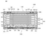
- FIG. 1 is a cross-sectional view schematically showing the configuration of a solid state battery module according to an embodiment.
- FIG. 2 schematically shows a cross-sectional view of the solid state battery module of FIG. 1 taken along a side surface 1300.
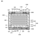
- FIG. 3 is a cross-sectional view schematically showing the configuration of a solid state battery module according to an embodiment.
- FIG. 4 schematically shows a cross-sectional view of the solid state battery module of FIG. 3 taken along a side surface 1300.
- FIG. 5 is a plan view schematically showing a coil section provided in a solid state battery module according to an embodiment.
- FIG. 6 is a plan view schematically showing a coil section provided in a solid state battery module according to an embodiment.
- FIG. 7 is a plan view schematically showing a coil section provided in a solid state battery module according to an embodiment.
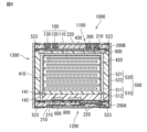
- FIG. 8 is a cross-sectional view schematically showing the configuration of a solid state battery module according to an embodiment.
- FIG. 9 schematically shows a cross-sectional view taken along a side surface 1300 of the solid state battery module of FIG.
- FIG. 10 is a plan view schematically showing the bottom surface of the solid state battery module according to one embodiment.
- FIG. 11A is a process cross-sectional view schematically showing one step in a method for manufacturing a solid-state battery module according to an embodiment of the present invention.
- FIG. 11B is a process cross-sectional view schematically showing one step in a method for manufacturing a solid-state battery module according to an embodiment of the present invention.
- FIG. 11A is a process cross-sectional view schematically showing one step in a method for manufacturing a solid-state battery module according to an embodiment of the present invention.
- FIG. 11B is a process cross
- FIG. 11C is a process cross-sectional view schematically showing one step in a method for manufacturing a solid-state battery module according to an embodiment of the present invention.
- FIG. 11D is a process cross-sectional view schematically showing one step in a method for manufacturing a solid-state battery module according to an embodiment of the present invention.
- FIG. 11E is a process cross-sectional view schematically showing one step in a method for manufacturing a solid-state battery module according to an embodiment of the present invention.
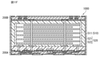
- FIG. 11F is a process cross-sectional view schematically showing one step in a method for manufacturing a solid-state battery module according to an embodiment of the present invention.
- solid battery module refers to a composite device composed of multiple parts including a solid battery, and in a narrow sense, it refers to a solid battery, a circuit element, and a composite device that includes a solid battery and a circuit element. It refers to a composite device consisting of connecting circuits and a board.
- cross-sectional view refers to the shape viewed from a direction substantially perpendicular to the stacking direction in the stacked structure of a solid-state battery (simply put, the cross-sectional view when cut along a plane parallel to the thickness direction of the layers) form).
- planar view used in this specification is based on a sketch when the object is viewed from above or below along the thickness direction of the layers (namely, the above-mentioned stacking direction).
- the vertically downward direction corresponds to the "downward direction"/"bottom side
- the opposite direction corresponds to the "upward direction"/"top side”. I can do it.
- the term "solid battery” refers to a battery whose constituent elements are made of solid matter, and in a narrow sense, it refers to an all-solid-state battery whose constituent elements are made of solid matter.
- the solid-state battery of the present invention is a stacked solid-state battery configured such that the layers constituting the battery constituent units are stacked on each other, and preferably each layer is made of a fired body.
- a “solid battery” includes not only a so-called “secondary battery” that can be repeatedly charged and discharged, but also a "primary battery” that can only be discharged.
- the "solid battery” is a secondary battery.
- the term “secondary battery” is not excessively limited by its name, and may include, for example, power storage devices. Note that, in the present invention, the solid-state battery included in the module can also be referred to as a "solid-state battery element.”
- FIG. 1 is a cross-sectional view schematically showing the configuration of a modular solid-state battery according to an embodiment of the present invention.
- FIG. 2 schematically shows a cross-sectional view of the solid state battery module of FIG. 1 taken along a side surface 1300.
- the solid battery 100 includes at least positive and negative electrode layers and a solid electrolyte.
- the solid battery 100 has a battery element including a battery structural unit consisting of a positive electrode layer 110, a negative electrode layer 120, and at least a solid electrolyte 130 interposed therebetween.
- each of its constituent layers may be formed by firing, and the positive electrode layer, negative electrode layer, solid electrolyte, etc. may form the fired layers.
- the positive electrode layer, the negative electrode layer, and the solid electrolyte are integrally fired with each other, and therefore, it is preferable that the battery element forms an integrally fired body.
- the positive electrode layer is an electrode layer containing at least a positive electrode active material.
- the positive electrode layer may further contain a solid electrolyte.
- the positive electrode layer may be composed of a fired body containing at least positive electrode active material particles and a solid electrolyte.
- the negative electrode layer is an electrode layer containing at least a negative electrode active material.
- the negative electrode layer may further contain a solid electrolyte.
- the negative electrode layer may be composed of a sintered body containing at least negative electrode active material particles and a solid electrolyte.
- a positive electrode active material and a negative electrode active material are materials that participate in the transfer of electrons in a solid battery. Ions move (conduct) between the positive electrode layer and the negative electrode layer via the solid electrolyte, and electrons are exchanged to perform charging and discharging. It is particularly preferable that each electrode layer of the positive electrode layer and the negative electrode layer is a layer capable of intercalating and deintercalating lithium ions or sodium ions. That is, the solid battery is preferably an all-solid-state secondary battery in which lithium ions or sodium ions move between a positive electrode layer and a negative electrode layer via a solid electrolyte to charge and discharge the battery.
- Examples of the positive electrode active material contained in the positive electrode layer include a lithium-containing phosphoric acid compound having a Nasicon-type structure, a lithium-containing phosphoric acid compound having an olivine-type structure, a lithium-containing layered oxide, and a lithium-containing phosphoric acid compound having a spinel-type structure. At least one selected from the group consisting of oxides and the like can be mentioned.
- An example of a lithium-containing phosphoric acid compound having a Nasicon type structure includes Li 3 V 2 (PO 4 ) 3 and the like.
- Examples of lithium-containing phosphate compounds having an olivine structure include Li 3 Fe 2 (PO 4 ) 3 , LiFePO 4 , and/or LiMnPO 4 .
- lithium-containing layered oxides examples include LiCoO 2 and/or LiCo 1/3 Ni 1/3 Mn 1/3 O 2 .
- Examples of lithium-containing oxides having a spinel structure include LiMn 2 O 4 and/or LiNi 0.5 Mn 1.5 O 4 .
- the type of lithium compound is not particularly limited, but may be, for example, a lithium transition metal composite oxide or a lithium transition metal phosphate compound.
- Lithium transition metal composite oxide is a general term for oxides containing lithium and one or more types of transition metal elements as constituent elements
- lithium transition metal phosphate compounds are oxides containing lithium and one or more types of transition metal elements as constituent elements. It is a general term for phosphoric acid compounds containing transition metal elements as constituent elements.
- the type of transition metal element is not particularly limited, and examples thereof include cobalt (Co), nickel (Ni), manganese (Mn), and iron (Fe).
- sodium-containing phosphoric acid compounds having a Nasicon-type structure sodium-containing phosphoric acid compounds having an olivine-type structure, sodium-containing layered oxides, and spinel-type structures are used. At least one selected from the group consisting of sodium-containing oxides and the like can be mentioned.
- the sodium-containing layered oxide may include at least one selected from the group consisting of 2FeP2O7 , Na4Fe3 ( PO4 ) 2 ( P2O7 ) , and NaFeO2 as the sodium - containing layered oxide.
- the positive electrode active material may be, for example, an oxide, a disulfide, a chalcogenide, or a conductive polymer.
- the oxide may be, for example, titanium oxide, vanadium oxide or manganese dioxide.
- the disulfide is, for example, titanium disulfide or molybdenum sulfide.
- the chalcogenide may be, for example, niobium selenide.
- the conductive polymer may be, for example, disulfide, polypyrrole, polyaniline, polythiophene, polyparastyrene, polyacetylene or polyacene.
- Examples of the negative electrode active material contained in the negative electrode layer include a group consisting of titanium (Ti), silicon (Si), tin (Sn), chromium (Cr), iron (Fe), niobium (Nb), and molybdenum (Mo).
- lithium alloy is Li-Al.
- lithium-containing phosphoric acid compounds having a Nasicon type structure include Li 3 V 2 (PO 4 ) 3 and/or LiTi 2 (PO 4 ) 3 .
- examples of the lithium-containing phosphoric acid compound having an olivine structure include Li 3 Fe 2 (PO 4 ) 3 and/or LiCuPO 4 .
- An example of a lithium-containing oxide having a spinel structure is Li 4 Ti 5 O 12 and the like.
- negative electrode active materials capable of intercalating and releasing sodium ions include sodium-containing phosphoric acid compounds having a Nasicon-type structure, sodium-containing phosphoric acid compounds having an olivine-type structure, and sodium-containing oxides having a spinel-type structure. At least one selected from the group consisting of:
- the positive electrode layer and the negative electrode layer may be made of the same material.
- the positive electrode layer and/or the negative electrode layer may contain a conductive material.
- the conductive material contained in the positive electrode layer and the negative electrode layer include at least one metal material such as silver, palladium, gold, platinum, aluminum, copper, and nickel, and carbon.
- the positive electrode layer and/or the negative electrode layer may contain a sintering aid.
- the sintering aid include at least one selected from the group consisting of lithium oxide, sodium oxide, potassium oxide, boron oxide, silicon oxide, bismuth oxide, and phosphorus oxide.
- the thickness of the positive electrode layer and the negative electrode layer is not particularly limited, but may be, for example, independently 2 ⁇ m or more and 50 ⁇ m or less, particularly 5 ⁇ m or more and 30 ⁇ m or less.
- the positive electrode layer and the negative electrode layer may each include a positive electrode current collecting layer and a negative electrode current collecting layer.
- the positive electrode current collecting layer and the negative electrode current collecting layer may each have a foil form. However, if more emphasis is placed on improving electronic conductivity through integral firing, reducing manufacturing costs of solid-state batteries, and/or reducing internal resistance of solid-state batteries, then the positive electrode current collecting layer and the negative electrode current collecting layer should each form a fired body. It may have.
- the positive electrode current collector constituting the positive electrode current collector layer and the negative electrode current collector constituting the negative electrode current collector it is preferable to use a material with high electrical conductivity, such as silver, palladium, gold, platinum, aluminum, copper, etc. , and/or nickel may be used.
- the positive electrode current collector and the negative electrode current collector may each have an electrical connection part for electrically connecting with the outside, and may be configured to be electrically connectable to the end surface electrode. Note that when the positive electrode current collecting layer and the negative electrode current collecting layer have the form of fired bodies, they may be constituted by fired bodies containing a conductive material and a sintering aid.
- the conductive material contained in the positive electrode current collection layer and the negative electrode current collection layer may be selected from the same materials as the conductive materials that may be contained in the positive electrode layer and the negative electrode layer, for example.
- the sintering aid contained in the positive electrode current collecting layer and the negative electrode current collecting layer may be selected from the same materials as the sintering aid that may be contained in the positive electrode layer and the negative electrode layer, for example.
- a positive electrode current collecting layer and a negative electrode current collecting layer are not necessarily required in a solid state battery, and a solid state battery that is not provided with such a positive electrode current collecting layer and a negative electrode current collecting layer is also conceivable. That is, the solid state battery included in the package of the present invention may be a solid state battery without a current collecting layer.
- a solid electrolyte is a material that can conduct lithium ions or sodium ions.
- the solid electrolyte layer that constitutes a battery constituent unit in a solid battery may form a layer between a positive electrode layer and a negative electrode layer that can conduct lithium ions.
- the solid electrolyte layer may be provided at least between the positive electrode layer and the negative electrode layer. That is, the solid electrolyte layer may be present around the positive electrode layer and/or the negative electrode layer so as to protrude from between the positive electrode layer and the negative electrode layer.
- the solid electrolyte contained in the solid electrolyte layer includes, for example, one or more of a crystalline solid electrolyte, a glass-based solid electrolyte, a glass-ceramic solid electrolyte, and the like.
- Examples of the crystalline solid electrolyte include oxide-based crystal materials and sulfide-based crystal materials.
- oxide-based crystal materials include lithium-containing phosphate compounds having a Nasicon structure, oxides having a perovskite structure, oxides having a garnet type or garnet-like structure, oxide glass ceramics-based lithium ion conductors, etc. It will be done.
- Lithium-containing phosphoric acid compounds having a Nasicon structure include Li x My (PO 4 ) 3 (1 ⁇ x ⁇ 2, 1 ⁇ y ⁇ 2, M is titanium (Ti), germanium (Ge), aluminum (Al ), gallium (Ga), and zirconium (Zr).
- An example of a lithium-containing phosphoric acid compound having a Nasicon structure includes Li 1.2 Al 0.2 Ti 1.8 (PO 4 ) 3 and the like.
- oxides having a perovskite structure include La 0.55 Li 0.35 TiO 3 and the like.
- oxides having a garnet type or garnet type similar structure includes Li 7 La 3 Zr 2 O 12 and the like.
- the sulfide-based crystal material include thio-LISICON, such as Li 3.25 Ge 0.25 P 0.75 S4 and Li 10 GeP 2 S 12 .
- the crystalline solid electrolyte may include a polymeric material (eg, polyethylene oxide (PEO), etc.).
- Examples of the glass-based solid electrolyte include oxide-based glass materials and sulfide-based glass materials.
- oxide glass material include 50Li 4 SiO 4 .50Li 3 BO 3 .
- Sulfide glass materials include , for example, 30Li 2 S.26B 2 S 3.44LiI, 63Li 2 S.36SiS 2.1Li 3 PO 4 , 57Li 2 S.38SiS 2.5Li 4 SiO 4 and 70Li 2 S. Examples include 30P 2 S 5 and 50Li 2 S.50GeS 2 .
- the glass-ceramic solid electrolyte examples include oxide-based glass-ceramic materials and sulfide-based glass-ceramic materials.
- oxide-based glass-ceramic material for example, a phosphoric acid compound (LATP) containing lithium, aluminum, and titanium as constituent elements, and a phosphoric acid compound (LAGP) containing lithium, aluminum, and germanium as constituent elements can be used.
- LATP is, for example, Li 1.07 Al 0.69 Ti 1.46 (PO 4 ) 3 .
- LAGP is, for example, Li 1.5 Al 0.5 Ge 1.5 (PO 4 ).
- examples of the sulfide-based glass ceramic materials include Li 7 P 3 S 11 and Li 3.25 P 0.95 S 4 .
- Examples of the solid electrolyte that can conduct sodium ions include sodium-containing phosphoric acid compounds having a Nasicon structure, oxides having a perovskite structure, and oxides having a garnet type or garnet type similar structure.
- the sodium-containing phosphate compound having a Nasicon structure includes Na x M y (PO 4 ) 3 (1 ⁇ x ⁇ 2, 1 ⁇ y ⁇ 2, M is from the group consisting of Ti, Ge, Al, Ga and Zr). at least one selected type).
- the solid electrolyte layer may contain a sintering aid.
- the sintering aid contained in the solid electrolyte layer may be selected from the same materials as the sintering aid contained in the positive electrode layer and the negative electrode layer, for example.
- the thickness of the solid electrolyte layer is not particularly limited.
- the thickness of the solid electrolyte layer located between the positive electrode layer and the negative electrode layer may be, for example, 1 ⁇ m or more and 15 ⁇ m or less, particularly 1 ⁇ m or more and 5 ⁇ m or less.
- Solid state batteries are generally provided with end electrodes 140.
- end electrodes 140 are provided on the side surfaces of the solid state battery. More specifically, an end surface electrode on the positive electrode side connected to the positive electrode layer and an end surface electrode on the negative electrode side connected to the negative electrode layer are provided (see FIG. 1).
- such end electrodes comprise a material with high electrical conductivity.
- Specific materials for the end electrodes are not particularly limited, but may include at least one selected from the group consisting of silver, gold, platinum, aluminum, copper, tin, and nickel.
- the solid state battery module may include a covering portion that covers the solid state battery.
- the covering portion is a layer that covers at least the periphery of the solid-state battery. As shown in FIGS. 1 and 2, the solid state battery 100 may be largely surrounded by the covering portion 500 as a whole. In other words, the solid battery 100 may be covered with the covering portion 500 so as to be completely surrounded.
- water vapor As used herein is not particularly limited to water in a gaseous state, but also includes water in a liquid state. In other words, the term “water vapor” is used to broadly encompass matters related to water, regardless of its physical state. Therefore, “water vapor” can also be referred to as water, and in particular, water in a liquid state may include condensed water, which is water in a gaseous state condensed.
- the covering portion may include an insulating covering layer and an inorganic covering layer located outside the insulating covering layer.
- the covering insulating layer 510 may be provided to cover the solid state battery 100 and the electronic component 600 on the first substrate.
- the solid battery 100 and the electronic component 600 may be largely surrounded by the covering insulating layer 510 as a whole.
- the covering inorganic layer 520 may be positioned further away from the solid state battery 100 than the covering insulating layer 510 is.
- the covering inorganic layer 520 may be provided so as to cover the covering insulating layer 510. Since the covering inorganic layer 520 is positioned outside the covering insulating layer 510, the covering inorganic layer 520 has a form of covering the periphery of the solid battery 100 together with the covering insulating layer 510.
- the covering insulating layer may be of any type as long as it exhibits insulating properties.
- the covering insulating layer corresponds to a resin layer. That is, it is preferable that the covering insulating layer contains a resin, and that this resin forms the base material of the layer.
- the covering insulating layer may be made of any material as long as it exhibits insulation properties.
- the covering insulating layer may contain a resin, and the resin may be either a thermosetting resin or a thermoplastic resin.
- the covering insulating layer may contain an inorganic filler.
- the covering insulating layer may be made of an epoxy resin containing an inorganic filler such as SiC, SiO 2 , or SiN.
- the resistivity of the covering insulating layer may be, for example, 10 6 ⁇ cm or more.
- the covering inorganic layer may have a film form, for example. Furthermore, the covering inorganic layer can also take the form of covering the side surfaces of the substrate.
- the insulating coating layer together with the inorganic coating layer forms a suitable water vapor barrier, and the inorganic coating layer also forms a suitable water vapor barrier together with the insulating coating layer.
- the term "barrier” as used herein means having a property of preventing water vapor permeation to such an extent that water vapor in the external environment does not pass through the substrate and cause deterioration of characteristics that are disadvantageous to the solid-state battery. In a narrow sense, this means that the water vapor permeability is less than 5 ⁇ 10 ⁇ 3 g/(m 2 ⁇ Day). To put it simply, the water vapor barrier layer preferably has a water vapor permeability of 0 or more and less than 5 ⁇ 10 ⁇ 3 g/(m 2 ⁇ Day).
- the material of the covering inorganic layer is not particularly limited, and may be metal, glass, oxide ceramics, or a mixture thereof.
- the inorganic coating layer comprises a metal component.
- the thickness of the coating inorganic layer may be 0.1 ⁇ m or more and 100 ⁇ m or less, for example, 1 ⁇ m or more and 50 ⁇ m or less.
- metal pad A metal pad may be interposed between the covering portion and the substrate in order to further strengthen the bond between the covering inorganic layer and the substrate.
- metal pads 523 may be provided on the first substrate 200A and the second substrate 200B, and the covering inorganic layer 520 may be provided so as to cover the metal pads 523.
- such metal pads 523 may be provided, for example, on the bottom side of the first substrate 200A and on the periphery of the top side of the second substrate 200B. Particularly when the substrate is made of ceramic or the like, it is preferable to provide metal pads.
- a solid state battery module 1000 includes a first substrate 200A having wiring, a solid state battery 100 disposed on the first substrate 200A, and an upper part of the solid state battery 100.
- a second board 200B that includes a coil section 300 arranged therein and electrically connectable to the first board 200A; is also located inside.
- the second substrate 200B which includes a coil section 300 that can be electrically connected to the first substrate, is disposed on the opposite side of the first substrate 200A with the solid battery 100 interposed therebetween.
- the first substrate 200A, the solid state battery 100, and the second substrate 200B are arranged in this order.
- the coil section 300 is provided inside the second substrate 200B.
- an induced current is generated in the coil section 300.
- the induced current flows to the solid state battery 100 via the first substrate 200A having wiring electrically connected to the coil part 300, and the solid state battery 100 is charged.
- the solid state battery module 1000 can be mounted on a mounting board via the first board 200A. Note that in this specification, an alternating magnetic field generated by alternating current may be simply referred to as a "magnetic field.”
- the module top surface means the module outer surface on the top side of the solid state battery module among the module outer surfaces that form the outer contour of the solid state battery module.
- the main surface of the solid state battery module 1000 that is relatively proximal to the second substrate 200B is the top surface 1100 of the solid state battery module.
- the top surface 1100 of the solid state battery module is also simply referred to as module top surface 1100.
- the main surface of the solid state battery module 1000 that is relatively proximal to the first substrate 200A is the bottom surface 1200 of the solid state battery module.
- the surface that connects the top surface 1100 of the solid state battery module and the bottom surface 1200 of the solid state battery module is the side surface 1300 of the solid state battery module.
- the side surface 1300 of the solid state battery module is also simply referred to as the module side surface 1300. Since the solid state battery module 1000 can be mounted on a mounting board via the first board 200A, the bottom surface 1200 of the solid state battery module can also be called a mounting surface.
- the top surface of the second board 200B is along the module top surface means that the top surface of the second board 200B and the module top surface are located on the same plane. Specifically, it means that among the main surfaces of the second substrate, the main surface that is relatively far from the solid battery and the module top surface are located on the same plane. Note that the top surface of the second substrate 200B means the main surface located on the proximal side with respect to the module top surface side, among the main surfaces of the second substrate.
- the top surface of the second substrate 200B which includes the coil portion 300 therein, is arranged inside the module top surface 1100.
- “Inner side of the module top surface” means the direction from the module top surface 1100 toward the inside of the solid state battery module 1000 (for example, the solid state battery 100).
- the solid battery module of the present disclosure can achieve the following effects.
- a solid-state battery module that has a wireless power feeding mechanism or a wireless communication mechanism requires a coil section for transmitting and receiving electromagnetic waves.
- the coil section may be arranged separately from the solid state battery module.
- the coil portion may be externally placed on the solid state battery module.
- the total size of the solid state battery module and the coil section may become large.
- the coil portion is positioned inside the second substrate.
- the top surface of the second substrate including the coil portion therein is positioned along the module top surface or inside the module top surface.
- the module top surface is the outer surface of the solid state battery module that forms the outer contour of the solid state battery module. Therefore, the top surface of the second substrate including the coil portion is located on the same plane as the outer surface of the solid-state battery module or inside the outer surface of the solid-state battery module. That is, the coil section is arranged inside the solid state battery module. In this arrangement of the coil portion, since a separate location for arranging the coil portion from the solid state battery module is not required, the total size of the solid state battery module and the coil portion can be reduced.
- the inductance value of the coil portion may be influenced by other components included in the solid-state battery module.
- wiring provided in a solid state battery module may itself have a unique inductance value.
- the inductance value of the coil portion connected to the wiring can be a composite inductance value with the inductance value unique to the wiring, and therefore can vary from the inductance value unique to the coil portion. Additionally, if the positional relationship between the coil part and other parts included in the solid-state battery module changes, the length between the coil part and other parts that can be connected to the coil part changes, so the inductance value of the coil part changes. It can change.
- the coil part is sometimes arranged separately from the solid-state battery module, so the location of the coil part can change for each solid-state battery module.
- the coil portion may be provided relatively more proximally or distally from the solid state battery module.
- the location of the coil section can be fixed. Since the arrangement location of the coil section can be fixed, it becomes easier to maintain a predetermined distance between the coil section and other components provided in the solid-state battery module. In other words, the inductance value of the coil portion of each solid battery module becomes more stable. When the inductance value becomes more stable, it becomes easier to match the LC frequency using the coil section and the capacitor in wireless power supply, and it becomes easier to efficiently charge the solid-state battery module.
- the solid state battery module of the present disclosure may further take the following aspects.
- the solid state battery module of the present disclosure includes a covering part that covers the solid-state battery, and since the covering part is the outermost part of the solid-state battery module, it can absorb alternating magnetic fields from the outside more than other parts.
- the sheath contains a metal component
- an external alternating magnetic field is more easily absorbed by the sheath than by the coil. Therefore, the alternating magnetic field may be difficult to transmit to the coil portion.
- a magnetic layer may be provided between the solid battery and the second substrate in order to make it easier to transmit the magnetic field to the coil portion.
- a magnetic layer may be provided between the solid battery and the coil section.
- the magnetic layer 700 is provided below the second substrate 200B. Since the magnetic layer 700 has a relatively higher magnetic permeability than other components constituting the solid-state battery module, it can act as a magnetic path for the magnetic flux passing through the coil section 300. By providing the magnetic layer 700 below the second substrate 200B, a relatively large amount of external magnetic field is easily attracted to the coil section built into the second substrate 200B above the magnetic layer 700. Become. In other words, it becomes easier to efficiently convert an external magnetic field into an induced current, and the charging efficiency of the solid-state battery can be improved.
- the thickness of the magnetic layer may be 50 ⁇ m or more, preferably 75 ⁇ m or more, more preferably 100 ⁇ m or more, and still more preferably 150 ⁇ m or more. From the viewpoint of reducing the thickness of the solid battery module, the thickness of the magnetic layer may be 500 ⁇ m or less, preferably 400 ⁇ m or less, more preferably 300 ⁇ m or less, and still more preferably 250 ⁇ m or less.
- the thickness of the magnetic layer may be thicker than the thickness of the electrode layer of the solid battery. Specifically, the thickness of the magnetic layer may be thicker than the positive electrode layer or negative electrode layer of the solid battery. From the viewpoint of attracting the magnetic field to the coil part, the thickness of the magnetic layer may be twice or more, preferably three times or more, more preferably five times or more, and even more preferably, the thickness of the positive electrode layer or the negative electrode layer. may be 8 times or more. From the viewpoint of reducing the thickness of the solid battery module, the thickness of the magnetic layer may be 25 times or less, preferably 20 times or less, more preferably 15 times or less, and even more preferably 13 times or less.
- the magnetic layer may be, for example, a layer containing a magnetic material and a resin.
- the magnetic material may be included in the magnetic layer in the form of particles.
- a resin a thermoplastic resin or a thermosetting resin may be used.
- a soft magnetic material may be used as the magnetic material included in the magnetic layer.
- the soft magnetic material may be iron, silicon steel, permalloy, sendust alloy, permendur, ferrite, amorphous magnetic alloy, magnetic stainless steel, or the like.
- the ferrite Ni-Zn-Cu ferrite, Mn-Zn ferrite, etc. may be used.
- thermoplastic resin contained in the magnetic layer at least one selected from the group consisting of polyamide resin, polycarbonate resin, polyphenylene sulfide resin, aromatic polyetherketone resin, and thermoplastic polyimide resin may be used.
- thermosetting resin contained in the magnetic layer one or more selected from the group consisting of epoxy resin, phenol resin, melamine resin, unsaturated polyester resin, silicone resin, and thermosetting polyimide resin may be used. good.
- the magnetic layer may be formed by rolling a mixture of the above magnetic material and the above resin to an arbitrary thickness and forming it into a plate shape, for example.
- a commercially available magnetic layer containing the above magnetic material and the above resin may be used.
- the magnetic layer may be arranged closer to the second substrate than the solid-state battery.
- the magnetic layer may be in contact with the second substrate side.
- the magnetic layer may have a relatively higher magnetic permeability than each component that constitutes the solid battery module. Therefore, the magnetic field from the outside can be absorbed more by the magnetic layer than by each component constituting the solid-state battery module. In other words, the magnetic layer can prevent an external magnetic field from being absorbed by each component constituting the solid-state battery module. In particular, it is possible to suppress absorption of a magnetic field to the outside by each component containing a metal component. From this point of view, it can be said that the magnetic layer is a layer for suppressing magnetic field absorption toward the metal side.
- the coil portion may be positioned inside the planar contour of the magnetic layer. Specifically, the coil portion may be positioned inside the region defined by the peripheral edge of the magnetic layer.
- the planar contour of the magnetic layer 700 is rectangular, and the coil portion 300 is positioned inside the rectangular planar contour formed by the magnetic layer 700.
- the first substrate and second substrate included in the solid state battery module of the present disclosure will be described below.
- a solid state battery module 1000 includes a first board 200A with wiring, a solid state battery 100 placed on the first board 200A, and a second board placed on the solid state battery 100.
- the second substrate 200B includes a first substrate 200A and an electrically connectable coil section 300 therein.
- the first board includes wiring and electronic components. Specifically, a plurality of electronic components are mounted on the first substrate, and each of the plurality of electronic components is electrically connected to each other by wiring provided on the first substrate. Each of the plurality of electronic components and the wiring provided on the first substrate are fixed with solder or the like.
- the first substrate may include a control circuit for controlling the solid state battery module, which is configured by wiring and a plurality of electronic components.
- the first substrate may be provided with battery terminal connection pins for electrically connecting the first substrate and the solid-state battery. As shown in FIG. 1, one of the battery terminal connection pins 142 is connected to the first substrate 200A, and the other of the battery terminal connection pins 142 is connected to the connection electrode 141. The connection electrode 141 is connected to the end surface electrode 140. The battery terminal connection pins 142 enable the transfer of electricity between the first substrate 200A and the solid state battery 100.
- a resist layer may be arranged on the first substrate. As shown in FIGS. 1 and 2, the resist layer 220 may be provided particularly on the main surface of the first substrate 200A.
- the resist layer 220 is a layer that at least partially covers the substrate surface to prevent physical processing or chemical reactions from occurring.
- a resist layer 220 is provided on the first substrate 200A, and a plurality of electronic components 600 are provided on the resist layer 220.
- a wiring 210 is provided in the resist layer 220.
- the wiring 210 of the resist layer 220 and the electronic component 600 are connected by solder 215 or the like.
- the plurality of electronic components 600 and the wiring 210 in the first substrate 200A are electrically connected via the wiring 210 in the resist layer 220.
- the second substrate includes a coil portion.
- the coil portion may include a portion provided on the second substrate, a portion provided inside the second substrate, and a portion exposed on the second substrate.
- the coil portion is mainly arranged inside the second substrate, and a portion thereof is positioned on the upper surface of the second substrate.
- the portion of the coil portion buried inside the second substrate is relatively larger than the portion exposed on the upper surface of the second substrate.
- a part of the coil portion does not necessarily need to be positioned on the upper surface of the second substrate, and the entire coil portion may be positioned inside the second substrate.
- the coil section 300 is connected to a wiring 210 provided on the second substrate 200B.
- Wiring 210 provided on the second substrate 200B is electrically connected to the first substrate 200A.
- the coil portion provided on the second substrate may be provided parallel to the second substrate.
- the coil portion may be provided in a stacked manner on the second substrate.
- the coil portion 300 may be configured to draw a spiral in a direction substantially parallel to the module top surface 1100. Since the coil portion 300 is covered with a resist layer 220 described later, it is located inside the module top surface 1100.
- a resist layer may be arranged on the second substrate. As shown in FIGS. 1 and 2, the resist layer 220 may be provided particularly on the main surface of the second substrate 200B.
- the resist layer 220 is a layer that at least partially covers the substrate surface to prevent physical processing or chemical reactions from occurring.
- a resist layer 220 is provided on the second substrate 200B.
- the resist layer 220 provided on the second substrate 200B becomes the outermost layer of the solid state battery module 1000 and can constitute at least the top surface 1100 of the module.
- a printed circuit board can be used as the first board and the second board.
- the type thereof is not particularly limited, and may be a resin substrate or a ceramic substrate.
- a rigid substrate or a flexible substrate may be used.
- the ceramic substrate include an alumina substrate, an LTCC substrate, or an HTCC substrate.
- the resin substrate may be made of a material in which a base material is impregnated with resin. Examples of the base material include paper, glass fiber cloth, and resin film.
- the resin may be a thermoplastic resin and/or a thermosetting resin.
- paper phenolic substrates are made by impregnating a paper base material with phenolic resin
- paper epoxy substrates are made by impregnating a paper base material with epoxy resin
- glass epoxy substrates are made by impregnating glass fiber cloth with epoxy resin
- polyimide and PET polyethylene terephthalate
- Examples include flexible substrates using talate resin.
- the wiring provided on the substrate may be made of at least one metal selected from the group consisting of Cu, Ni, Ag, Au, and Pt.
- the first substrate is preferably a member for electrically connecting the modular solid-state battery to the outside.
- the substrate serves as a terminal substrate for the external terminals of the solid-state battery.
- FIG. 10 shows the bottom surface 1200 of the solid state battery module.
- the bottom surface 1200 is the main surface of the first substrate.
- the first substrate is provided with a back pad (specifically, metal foil) 211 that can function as an external terminal.
- the solid state battery can be mounted on another secondary substrate such as a printed wiring board with the substrate interposed therebetween.
- the solid state battery module of the present invention is preferably an SMD (Surface Mount Device) type battery module.
- the covering inorganic layer when a solid state battery module is provided with a covering inorganic layer, the covering inorganic layer may be provided along a side surface of the solid state battery module. In other words, the covering inorganic layer may constitute at least the module side part.
- the covering inorganic layer 520 is provided so as to cover each side surface 1300 of the solid state battery module 1000. Specifically, the covering inorganic layer 520 covers the covering insulating layer 510 surrounding the solid battery 100, the side surface of the first substrate, and the side surface of the second substrate.
- the covering inorganic layer 520 may entirely cover each side surface 1300 of the solid state battery module 1000.
- the covering inorganic layer may be provided along the top surface of the solid state battery module. Specifically, the covering inorganic layer may be provided so as to cover a part of the top surface of the solid state battery module.
- the covering inorganic layer 520 is provided so as to cover the periphery (or peripheral portion) of the module top surface 1100.
- the contour shape of the covering inorganic layer 520 covering the module top surface 1100 corresponds to the contour of the module top surface 1100.
- the outline of the covering inorganic layer 520 covering the module top surface 1100 is rectangular and annular.
- the outline of the covering inorganic layer 520 covering the module top surface 1100 is rectangular and annular, it has an outer outline forming the outer outline of the "ring” and an inner outline forming the inner outline of the "ring".
- the covering inorganic layer 520 includes a discontinuous region of the covering inorganic layer 520 on the module top surface 1100 side.
- “Discontinuous region” means a region including a portion covered by the covering inorganic layer 520 and a portion not covered by the covering inorganic layer 520.
- a continuous region of the covering inorganic layer 520 is formed because the covering inorganic layer 520 covers the entire module side surface 1300.
- the covering inorganic layer 520 covers not the entire module top surface 1100 but a part of the top surface, a discontinuous region of the covering inorganic layer is formed. In other words, it can be said that a part of the second substrate 200B is exposed on the module top surface 1100 side.
- the coil portion provided inside the second substrate is less likely to be covered by the covering inorganic layer. Therefore, the coil portion becomes more susceptible to external magnetic fields, and the charging efficiency of the solid-state battery can be further improved.
- the covering inorganic layer may be provided along the bottom surface of the solid state battery module.
- the form of the inorganic coating layer provided on the bottom surface of the module may be similar to the form of the inorganic coating layer provided on the top surface of the module.
- the covering inorganic layer covers the module side surface and may constitute a part of at least one of the module top surface and the module bottom surface that are continuous with the module side surface.
- the inorganic coating layer 520 that covers the module top surface 1100 is continuous with the inorganic coating layer 520 that covers the module side surface 1300.
- the covering inorganic layer 520 covers the side surface of the second substrate 200B and further covers a part of the upper main surface of the second substrate 200B that is continuous with the side surface of the second substrate 200B. I can say that.
- the covering inorganic layer 520 covers the side surface of the first substrate 200A and further covers a part of the upper main surface of the first substrate 200A that is continuous with the side surface of the first substrate 200A.
- the outer contour of the magnetic layer may be on or inside the inner contour of the covering inorganic layer.
- the outer contour of the magnetic layer may overlap the inner contour of the covering inorganic layer and may be located within the region defined by the inner contour of the covering inorganic layer.
- the outer contour of the magnetic layer 700 is surrounded by the inner contour of the covering inorganic layer 520.
- the portion corresponding to the outer contour of the magnetic layer 700 in FIG. 5 is located inside the portion corresponding to the inner contour of the covering inorganic layer 520 in FIG.
- the portion corresponding to the outer contour of the magnetic layer 700 and the portion corresponding to the inner contour of the covering inorganic layer 520 do not overlap with each other.
- the inorganic coating layer is not positioned on the magnetic layer 700, so that the magnetic field attracted to the magnetic layer 700 and the magnetic field exiting from the magnetic layer 700 are difficult to be absorbed by the inorganic coating layer. Become. Therefore, it becomes easier to efficiently convert a magnetic field into an induced current, and the charging efficiency of the solid-state battery can be improved.
- the planar contour of the magnetic layer may be surrounded by a covering inorganic layer.
- the covering inorganic layer may be positioned outside the region defined by the peripheral edge of the magnetic layer.
- the planar contour of the magnetic layer means the contour shape when the magnetic layer is viewed in plan.
- the planar contour of the magnetic layer 700 is rectangular, and the covering inorganic layer 520 is positioned outside the planar contour of the magnetic layer 700.
- the covering insulating layer may include a solid battery sealing layer that covers the solid battery and an electronic component sealing layer that covers the electronic component provided on the substrate.
- the solid state battery 100 is covered with a solid state battery sealing layer 511.
- the electronic component 600 on the first substrate 200A is covered with an electronic component sealing layer 512.
- the material of the solid battery sealing layer 511 and the electronic component sealing layer 512 may be the material of the covering insulating layer exemplified above.
- the coating inorganic layer may include a metal thin film and a metal plating layer.
- the metal thin film 521 may be provided in contact with the covering insulating layer 510.
- the metal plating layer 522 is provided outside the metal thin film 521, in other words, it may be positioned further away from the solid battery 100 than the metal thin film 521 is.
- the metal thin film may be a dry plating layer, specifically a sputtered film. That is, the solid state battery module of the present invention may be provided with a sputtered film as a metal thin film.
- a sputtered film is a thin film obtained by sputtering. In other words, a film deposited by sputtering ions onto a target and knocking out the atoms can be used as the dry plating layer.
- the sputtered film has a very thin form on the nano- or micro-order, it becomes a relatively dense and/or homogeneous layer, so it can contribute to preventing water vapor permeation for solid-state batteries. Furthermore, since the sputtered film is formed by atomic deposition, it can be more appropriately deposited on the target. Therefore, the sputtered film can be more suitably used as a barrier that prevents water vapor in the external environment from entering the solid state battery. Therefore, when the covering inorganic layer further includes a sputtered film as a dry plating layer, it is possible to further improve the ability to prevent water vapor from permeating into the solid-state battery.
- the dry plating layer may be formed by other dry plating methods such as a vacuum evaporation method or an ion plating method.
- the dry plating layer may contain at least one selected from the group consisting of, for example, Al (aluminum), Cu (copper), Ti (titanium), and stainless steel (SUS).
- the thickness of the metal thin film is preferably 1 ⁇ m or more and 10 ⁇ m or less, more preferably 2 ⁇ m or more and 8 ⁇ m or less, and even more preferably 3 ⁇ m or more and 6 ⁇ m or less.
- the metal plating layer may be a wet plating layer. As shown in FIG. 1, metal plating layer 522 forms the outermost layer of covering inorganic layer 520. Since the metal plating layer 522 can be exposed to the external environment, it may have deterioration resistance.
- the metal plating layer 522 preferably contains at least one metal selected from the group consisting of Ni (nickel), Cr (chromium), Pd (palladium), Pt (platinum), and Zn.
- the thickness of the metal plating layer is preferably 1 ⁇ m or more and 20 ⁇ m or less, more preferably 2 ⁇ m or more and 15 ⁇ m or less, and particularly preferably 2 ⁇ m or more and 10 ⁇ m or less. By setting the thickness of the metal plating layer within the above range, deterioration of the plating layer can be suitably reduced.
- the first substrate and the coil section are electrically connected to each other.
- the solid battery module 1000 further includes a connection wiring 400 that connects the first substrate 200A and the coil section 300, thereby electrically connecting the first substrate 200A and the coil section 300. has been done.
- the connection wiring 400 is arranged so as to run along the wall surface of the solid state battery 100.
- the connection wiring 400 is provided so as to cross the solid state battery 100, and the connection wiring 400 is connected to the first substrate 200A via the antenna circuit connection pin 450. Therefore, the coil portion and the solid state battery are electrically connected via the connection wiring.
- connection wiring 400 With this arrangement of the connection wiring 400, the induced current generated in the coil section 300 can be sent to the first substrate 200A. Further, as shown in FIG. 1, since the electronic component 600 is placed on the main surface of the first substrate 200A, the induced current generated in the coil section 300 is supplied to the electronic component. In this respect, it can be said that the coil section 300 and the electronic component 600 are electrically connected via the connection wiring 400.
- FIG. 6 shows the positional relationship between the coil portion 300 and the connection wiring 400 in FIGS. 1 and 2.
- the connection wiring 400 connects the first substrate 200A and the coil section 300, and the connection wiring 400 and the coil section 300 are connected via the connection pins 350.
- a connecting pin 350 is provided on the coil portion.
- a connection wiring 400 is connected to the connection pin 350 (not shown).
- four connection pins 350 are provided on the coil portion 300, four connection wirings are provided on the coil portion 300 via the connection pins.
- connection pin 350 provided on the coil portion 300 the installation location of the connection wiring 400 provided on the solid state battery module 1000 can be changed.
- the number of connection pins 350 provided in the coil section 300 the number of connection wires 400 provided in the solid state battery module 1000 can be changed. For example, as shown in FIG. 8, by setting the number of connection pins installed in the coil portion 300 to two, the number of connection wirings installed can be set to two.
- the coil portion and the metal wiring may be connected by a connecting pin, and the position where the connection wiring is provided may be adjusted.
- a metal wiring 370 is provided at the tip of the coil portion 300.
- the coil portion 300 and the metal wiring 370 are fixed by a connecting pin 360.
- another metal wiring 375 may be provided on the metal wiring 370.
- connection wirings may be provided in the solid state battery module.
- the connection wiring may be provided along only one side of the solid state battery module, or may be provided along two or more sides.
- one or more connection wirings may be provided along one side surface.
- FIG. 1 shows a cross-sectional view taken along the side of a solid state battery module 1000.
- two connection wires 400 are arranged on the side surface of the solid battery 100.
- FIG. 2 shows a cross-sectional view of the solid state battery module 1000 taken along the module side surface 1300 shown in FIG.
- two connection wires 400 are arranged on the side surface of the solid state battery 100. That is, the solid state battery module 1000 shown in the embodiments of FIGS. 1 and 2 is provided with a total of four connection wires 400.
- the solid state battery module may be provided with connection wiring that is U-shaped (or U-shaped). In other words, the solid state battery module may be provided with connection wiring having a plurality of bent portions.
- FIG. 8 is a cross-sectional view schematically showing the configuration of a solid state battery module according to an embodiment.
- FIG. 9 schematically shows a cross-sectional view of the solid state battery module of FIG. 8 taken along a side surface 1300.
- two or more connection wires are arranged in the solid state battery module 1000.
- the first connection wiring 410 and the second connection wiring 420 extend in the first direction from the first substrate 200A toward the coil section 300.
- a third connection wiring 430 connecting the first connection wiring 410 and the second connection wiring 420 is arranged.
- the third connection wiring 430 extends in a second direction that intersects with the first direction.
- the first connection wiring 410, the second connection wiring 420, and the third connection wiring 430 form a connection wiring whose appearance is U-shaped (or U-shaped). ing. In other words, a connection wiring having two bent portions is formed.
- the connection wiring having such a configuration is provided so as to straddle the solid-state battery.
- connection wiring composed of the first, second, and third connection wirings is provided on the first substrate
- the first connection wiring and the second connection wiring can be positioned on the first substrate at the same time.
- it becomes easier to provide the first connection wiring and the second connection wiring on the first board at the same time so Manufacturing of the battery module becomes easier and manufacturing efficiency can be improved.
- a water-resistant barrier film may be provided between the substrate and the solid state battery. As shown in FIG. 1, a water-resistant barrier film 800 may be provided between the first substrate 200A and the solid-state battery 100, and/or a water-resistant barrier film 800 may be provided between the second substrate 200B and the solid-state battery 100. may be provided. By providing the water-resistant barrier film 800, undesirable permeation of water vapor from the external environment to the solid-state battery via the substrate is reduced, so that deterioration of the solid-state battery characteristics can be reduced in the long term.
- the water-resistant barrier film 800 is provided on the main surface of the first substrate 200A that is proximal to the solid battery 100. Similarly, the water-resistant barrier film 800 is provided on the main surface of the second substrate that is proximal to the solid battery.
- the water-resistant barrier film 800 provided on the first substrate 200A and the second substrate 200B is provided along the main surface of each substrate. The peripheral edge of the water-resistant barrier film 800 may be in contact with the covering inorganic layer 520. Further, the main surface of the water-resistant barrier film 800 is provided so as to be in contact with the covering insulating layer 510. In the case of the embodiment having the magnetic layer 700 shown in FIGS. 3 and 4, the water-resistant barrier film 800 may be provided between the magnetic layer 700 and the second substrate 200B.
- the water-resistant barrier film is not particularly limited as long as it is made of a material that exhibits insulation properties, and specific examples of such materials include glass, inorganic insulators such as alumina, and organic insulators such as resin. One type may be used alone, or two or more types may be used in combination.
- the first board may include a wireless power supply circuit.
- the wireless power supply circuit may include wiring, a plurality of electronic components, and a coil section provided inside the second substrate.
- the wireless power supply circuit consists of a plurality of circuits.
- the wireless power supply circuit may include a power receiving circuit, a step-up/down circuit, and a battery charging circuit.
- Power can be wirelessly transmitted to the power receiving circuit from the outside (for example, a power transmitting unit).
- the power receiving circuit may include a coil section provided on the second substrate, a capacitor, a resistor, and a rectifier circuit.
- the coil section provided on the second substrate generates an induced current by receiving electromagnetic waves from the outside.
- the rectifier circuit rectifies the induced current generated in the coil section and converts alternating current to direct current.
- the rectifier circuit may be a diode bridge circuit.
- a smoothing capacitor may be connected to the output of the rectifier circuit, so that the output voltage output from the rectifier circuit can be smoothed.
- the buck-boost circuit converts the input voltage.
- a rectified and smoothed voltage may be input to the buck-boost circuit.
- a DC-DC converter, an LDO (low dropout regulator), or the like may be used as the step-up/down circuit.
- a smoothing capacitor may be connected to the output of the buck-boost circuit, and the output voltage output from the buck-boost circuit can be smoothed.
- the smoothed output voltage of the buck-boost circuit is input to a battery charging circuit that controls charging of the solid-state battery.
- the output voltage from the battery charging circuit may be smoothed by a smoothing capacitor, and the solid state battery can be charged by inputting the output voltage to the solid state battery.
- the wireless power supply circuit may further include other circuits.
- a wireless communication (wi-fi, Bluetooth, NFC, RF-ID, Zig-Bee, and/or specified low power wireless, etc.) circuit, protection circuit, current path circuit, and/or sensor circuit, etc. may be provided. .
- the solid state battery module may include a resonant circuit.
- the coil portion and the capacitor provided on the first substrate may resonate.
- the capacitor and the coil section resonate (that is, match) at a predetermined frequency.
- the coil portion and the capacitor may be connected in parallel. Since the received current can increase due to resonance between the capacitor and the coil, an external magnetic field can be more efficiently converted into an induced current, and the charging efficiency of the solid-state battery can be improved.
- the solid-state battery module of the present disclosure can be obtained by preparing a solid-state battery including a battery constituent unit having a positive electrode layer, a negative electrode layer, and a solid electrolyte between these electrodes, and then going through a process of modularizing the solid-state battery. Obtainable.
- the production of the solid-state battery of the present invention can be broadly divided into the production of the solid-state battery itself (hereinafter also referred to as "pre-module battery"), which corresponds to the preliminary stage of modularization, preparation of the substrate, and modularization. .
- the pre-module battery can be manufactured by a printing method such as a screen printing method, a green sheet method using a green sheet, or a combination thereof.
- the pre-module battery itself may be manufactured according to a conventional manufacturing method for solid-state batteries (therefore, the solid electrolyte, organic binder, solvent, optional additives, positive electrode active material, negative electrode active material, etc. described below), etc.
- the raw materials used in the production of known solid-state batteries may be used).
- (Laminated block formation) Prepare a slurry by mixing the solid electrolyte, organic binder, solvent, and optional additives. Next, a sheet containing a solid electrolyte is formed from the prepared slurry by firing. ⁇ Create a positive electrode paste by mixing the positive electrode active material, solid electrolyte, conductive material, organic binder, solvent, and optional additives. Similarly, a negative electrode paste is prepared by mixing a negative electrode active material, a solid electrolyte, a conductive material, an organic binder, a solvent, and any additives. - Print a positive electrode paste on the sheet, and also print a current collecting layer and/or a negative layer as necessary.
- a negative electrode paste is printed on the sheet, and if necessary, a current collecting layer and/or a negative layer are printed.
- a laminate by alternately stacking sheets printed with positive electrode paste and sheets printed with negative electrode paste.
- the outermost layer (the uppermost layer and/or the lowermost layer) of the laminate may be an electrolyte layer, an insulating layer, or an electrode layer.
- the laminate is crimped and integrated, it is cut into a predetermined size.
- the obtained cut laminate is subjected to degreasing and firing. Thereby, a fired laminate is obtained.
- the laminate may be degreased and fired before cutting, and then the laminate may be cut.
- the end electrode on the positive electrode side can be formed by applying a conductive paste to the exposed side surface of the positive electrode in the fired laminate.
- the end electrode on the negative electrode side can be formed by applying a conductive paste to the exposed side surface of the negative electrode in the fired laminate.
- the end face electrodes on the positive electrode side and the negative electrode side may be provided so as to extend to the main surface of the fired laminate.
- the component of the end electrode may be selected from at least one selected from silver, gold, platinum, aluminum, copper, tin, and nickel. Note that antimony, bismuth, indium, zinc, aluminum, etc., which form an alloy with tin, may be included.
- end electrodes on the positive electrode side and the negative electrode side are not limited to being formed after firing the laminate, but may be formed before firing and subjected to simultaneous firing.
- a desired pre-module battery (corresponding to the solid battery 100) can finally be obtained.
- the substrate is prepared.
- a resin substrate when used as the substrate, it may be prepared by laminating a plurality of layers and subjecting them to heating and pressure treatment.
- a substrate precursor is formed using a resin sheet made by impregnating a fiber cloth serving as a base material with a resin raw material. After forming the substrate precursor, the substrate precursor is heated and pressurized using a press.
- a ceramic substrate when used as a substrate, its preparation is, for example, by thermocompression bonding a plurality of green sheets to form a green sheet laminate, and by subjecting the green sheet laminate to firing to obtain a ceramic substrate. I can do it.
- the ceramic substrate can be prepared, for example, in accordance with the preparation of an LTCC substrate.
- a semirac substrate may have vias and/or lands.
- holes may be formed in the green sheet using a punch press or carbon dioxide laser, and the holes may be filled with conductive paste material, or a printing method using conductive paste material or solder may be used.
- Precursors of conductive parts such as vias and lands may be formed by this method. Note that the lands and the like can also be formed after the green sheet laminate is fired.
- the second substrate may be prepared by the same method as the method for preparing the first substrate.
- the coil inside the second substrate may be provided inside the second substrate by arranging a conductive material such as wiring in a spiral or spiral shape.
- the second substrate including the coil portion therein may be prepared by patterning a conductive paste material in a spiral or spiral shape on the substrate using a printing method or the like.
- the second substrate including the coil portion therein may be a single substrate or a stack of substrates formed with a spiral or spiral pattern of conductive paste material.
- At least the electronic component 600 such as a capacitor, the battery terminal connection pin 142, etc. are placed on the wiring 210 located at a predetermined location on the first substrate 200A (see FIG. 11A).
- the wiring 210 located at a predetermined location on the first substrate 200A, the electronic component 600, etc. may be fixed with solder 215 or the like.
- a covering portion (for example, the electronic component sealing layer 512) is formed on the first substrate 200A on which the electronic component 600, the battery terminal connection pin 142, etc. are placed.
- the raw material for the insulating coating layer is provided so that the electronic components and the like are completely covered.
- the covering insulating layer is made of a resin material
- the electronic component sealing layer may be formed by providing a resin precursor on the substrate and subjecting it to curing.
- the electronic component sealing layer at least a portion of the battery terminal connection pin 142 is not covered with the electronic component sealing layer and is exposed.
- a conductive connection electrode 141 is printed on the exposed battery terminal connection pin 142 (see FIG. 11B).
- the solid battery 100 coated with the end electrode 140 specifically, a "non-modular solid state battery" is mounted on the first substrate 200A so that the end electrode 140 and the connection electrode 141 are connected. See (FIG. 11C).
- connection wiring 400 is connected to the connection electrode 141 so as to straddle the solid state battery 100 (see FIG. 11D).
- the second substrate 200B is placed on top of the solid battery (see FIG. 11E). Specifically, the second substrate 200B is positioned above the solid-state battery, and the second substrate 200B and the connection wiring 400 are connected. More specifically, the second substrate 200B is positioned above the solid battery so that the wiring 210 provided on the second substrate 200B and the connection wiring 400 are connected.
- an insulating cover layer (for example, solid battery sealing layer 511) is formed (see FIG. 11F).
- the raw material for the covering insulating layer is provided so that the solid battery 100 on the first substrate 200A is completely covered.
- the insulating cover layer is made of a resin material
- a resin precursor is provided on the substrate and cured to form the insulating cover layer (for example, the solid battery sealing layer 511).
- the solid battery sealing layer may be molded by applying pressure with a mold.
- a solid state battery encapsulant layer that encapsulates a solid state battery on a substrate may be formed through compression molding.
- the raw material for the solid battery sealing layer may be in the form of granules, and may be thermoplastic. Note that such molding is not limited to mold molding, and may be performed through polishing, laser processing, and/or chemical treatment. As a result of the above, the solid state battery is positioned between the first substrate and the second substrate.
- a covering inorganic layer 520 is formed (see FIG. 11F). Specifically, a covering inorganic layer 520 (for example, a metal thin film 521) is formed on "a coating precursor in which a solid battery is covered with a solid battery sealing layer on a first substrate".
- the metal thin film 521 may be formed by dry plating, for example, to form a dry plating film as a metal thin film. More specifically, dry plating is performed to coat the coating precursor and the exposed surfaces of each of the first and second substrates (i.e., other than the bottom surface of the first substrate and the top surface of the second substrate). to form a metal thin film.
- a metal plating layer 522 is formed outside the metal thin film 521 (see FIG. 11F). Specifically, a metal plating layer 522 is formed to cover the metal thin film 521.
- the metal plating layer 522 may be formed by performing wet plating. More specifically, wet plating is performed to form a metal plating layer so as to cover the coating precursor and the metal thin film covering each side of the first substrate and the second substrate. Furthermore, the metal plating layer may be formed to cover a portion of the bottom surface of the first substrate and/or the top surface of the second substrate. Specifically, the metal plating layer may be formed to cover the peripheral edge of the bottom surface of the first substrate and/or the peripheral edge of the top surface of the second substrate.
- a magnetic layer may be provided in order to make the coil provided inside the second substrate more susceptible to external magnetic fields.
- the magnetic layer can be obtained, for example, by rolling a mixture of magnetic powder and resin to a desired thickness and forming it into a plate shape. Further, the magnetic layer can also be cut to any size.
- the magnetic layer obtained by the above method can be provided, for example, during the step of arranging the second substrate on top of the solid battery.
- a magnetic layer cut to an arbitrary size may be placed on a second substrate, and the second substrate provided with the magnetic layer may be placed on top of the solid battery.
- the second substrate provided with the magnetic layer may be placed on top of the solid-state battery so that the magnetic layer provided on the second substrate and the solid-state battery face each other.
- the magnetic layer may be attached to the second substrate using an adhesive or the like.
- the solid-state battery module By going through the steps described above, it is possible to obtain a module product in which the solid-state battery on the substrate is covered with the covering part.
- the "solid battery module” according to the present invention can finally be obtained. Since the solid-state battery module obtained through this process has the coil portion provided inside the second substrate, the total size of the solid-state battery module and the coil portion tends to be relatively small. Furthermore, since the position of the coil part is easily fixed, the inductance value of the coil part is easily stabilized, and it is possible to reduce the need to perform matching for each solid-state battery module. Therefore, it becomes possible to efficiently perform wireless power supply and the like.
- aspects of the solid state battery module of the present disclosure are as follows. ⁇ 1> a first board having wiring; a solid state battery disposed on the first board; and a second board internally including a coil section disposed above the solid state battery and electrically connectable to the first board.
- a solid battery module comprising: a top surface of the second substrate is positioned along a top surface of the module or inside the top surface of the module.
- a magnetic layer is provided between the solid battery and the second substrate.
- the magnetic layer is disposed closer to the second substrate than the solid battery.
- ⁇ 4> The solid battery module according to ⁇ 2> or ⁇ 3>, wherein the magnetic layer is in contact with the second substrate side.
- ⁇ 5> The solid state battery module according to any one of ⁇ 2> to ⁇ 4>, wherein the coil portion is positioned inside a planar contour of the magnetic layer.
- the solid-state battery is further provided with a coating portion that covers the solid-state battery, the coating portion including an insulating coating layer and an inorganic coating layer located outside the insulating coating layer, and the planar outline of the magnetic layer is similar to the inorganic coating layer.
- the solid battery module according to any one of ⁇ 2> to ⁇ 5> which is surrounded by.
- ⁇ 7> The solid battery module according to ⁇ 6>, wherein the outer contour of the magnetic layer is on the inner contour of the covering inorganic layer or inside the inner contour in cross-sectional view.
- ⁇ 8> The solid-state battery according to any one of ⁇ 2> to ⁇ 7>, wherein the solid-state battery includes an electrode layer, and the thickness of the magnetic layer is thicker than the thickness of the electrode layer of the solid-state battery.
- module. ⁇ 9> The solid battery module according to any one of ⁇ 2> to ⁇ 8>, wherein the magnetic layer is a magnetic field attraction layer to the coil portion.
- the magnetic layer is a metal absorption suppressing layer.
- ⁇ 11> Further comprising a covering part that covers the solid-state battery, the covering part including a covering insulating layer and a covering inorganic layer located outside the covering insulating layer, and on the top surface side of the module, the covering part includes a covering inorganic layer located outside the covering inorganic layer.
- the solid state battery module according to any one of ⁇ 1> to ⁇ 5>, including a continuous region.
- ⁇ 12> The solid battery module according to ⁇ 11>, wherein the covering inorganic layer constitutes at least a side surface portion of the module.
- ⁇ 13> The solid battery module according to ⁇ 11> or ⁇ 12>, wherein the covering inorganic layer further constitutes a part of at least one of a module top surface and a module bottom surface that are continuous with the module side surface.
- the covering inorganic layer covers at least a side surface of the second substrate.
- the coating inorganic layer further covers a part of the upper main surface of the second substrate that is continuous with a side surface of the second substrate. module.
- connection wirings Two or more of the connection wirings are arranged, the first and second connection wirings extend in a first direction from the first substrate toward the coil part, and the first and second connection wirings extend in a first direction from the first substrate toward the coil part.
- the solid state battery module of the present invention can be used in various fields where battery use or power storage is expected. Although this is just an example, the solid state battery module of the present invention can be used in the electrical, information, and communication fields where mobile devices are used (e.g., mobile phones, smartphones, notebook computers, digital cameras, activity meters, arm computers, electronic paper, RFID tags, card-type electronic money, small electronic devices such as smart watches, electrical/electronic equipment field or mobile equipment field), home/small industrial applications (e.g., power tools, golf carts, household/electronic equipment field), nursing care/industrial robots), large industrial applications (e.g. forklifts, elevators, harbor cranes), transportation systems (e.g.
- mobile devices e.g., mobile phones, smartphones, notebook computers, digital cameras, activity meters, arm computers, electronic paper, RFID tags, card-type electronic money, small electronic devices such as smart watches, electrical/electronic equipment field or mobile equipment field
- home/small industrial applications e.g., power tools, golf carts, household
- hybrid cars electric cars, buses, trains, electrically assisted bicycles, electric motorcycles, etc.
- power system applications e.g., various power generation, road conditioners, smart grids, home-installed electricity storage systems, etc.
- medical applications medical equipment such as earphones and hearing aids
- pharmaceutical applications medication management systems, etc.
- IoT field space and deep sea applications (for example, in the fields of space probes, underwater research vessels, etc.).
- Solid battery 110 Positive electrode layer 120 Negative electrode layer 130 Solid electrolyte 140 End electrode 141 Connection electrode 142 Battery terminal connection pin 200A First substrate 200B Second substrate 210 Wiring 211 Back pad 215 Solder 220 Resist layer 300 Coil part 350 Connection pin 400 Connection wiring 410 First connection wiring 420 Second connection wiring 430 Third connection wiring 450 Antenna circuit connection pin 500 Covering portion 510 Covering insulating layer 511 Solid battery sealing layer 512 Electronic component sealing layer 520 Covering inorganic layer 521 Metal thin film 522 Metal plating layer 523 Metal pad 600 Electronic component 700 Magnetic layer 800 Water-resistant barrier film 1000 Solid battery module 1100 Top surface of solid battery module 1200 Bottom surface of solid battery module 1300 Side surface of solid battery module
Landscapes
- Chemical & Material Sciences (AREA)
- General Chemical & Material Sciences (AREA)
- Chemical Kinetics & Catalysis (AREA)
- Electrochemistry (AREA)
- Engineering & Computer Science (AREA)
- Manufacturing & Machinery (AREA)
- Inorganic Chemistry (AREA)
- Materials Engineering (AREA)
- General Physics & Mathematics (AREA)
- Condensed Matter Physics & Semiconductors (AREA)
- Physics & Mathematics (AREA)
- Composite Materials (AREA)
- Secondary Cells (AREA)
Priority Applications (2)
| Application Number | Priority Date | Filing Date | Title |
|---|---|---|---|
| JP2024542652A JP7708321B2 (ja) | 2022-08-25 | 2023-07-19 | 固体電池モジュール |
| US19/040,181 US20250192253A1 (en) | 2022-08-25 | 2025-01-29 | Solid-state battery module |
Applications Claiming Priority (2)
| Application Number | Priority Date | Filing Date | Title |
|---|---|---|---|
| JP2022134463 | 2022-08-25 | ||
| JP2022-134463 | 2022-08-25 |
Related Child Applications (1)
| Application Number | Title | Priority Date | Filing Date |
|---|---|---|---|
| US19/040,181 Continuation US20250192253A1 (en) | 2022-08-25 | 2025-01-29 | Solid-state battery module |
Publications (1)
| Publication Number | Publication Date |
|---|---|
| WO2024042927A1 true WO2024042927A1 (ja) | 2024-02-29 |
Family
ID=90013238
Family Applications (1)
| Application Number | Title | Priority Date | Filing Date |
|---|---|---|---|
| PCT/JP2023/026428 Ceased WO2024042927A1 (ja) | 2022-08-25 | 2023-07-19 | 固体電池モジュール |
Country Status (3)
| Country | Link |
|---|---|
| US (1) | US20250192253A1 (https=) |
| JP (1) | JP7708321B2 (https=) |
| WO (1) | WO2024042927A1 (https=) |
Citations (2)
| Publication number | Priority date | Publication date | Assignee | Title |
|---|---|---|---|---|
| WO2021070598A1 (ja) * | 2019-10-11 | 2021-04-15 | 株式会社村田製作所 | ワイヤレス充電固体電池モジュール及びワイヤレス電源モジュール |
| WO2021070468A1 (ja) * | 2019-10-11 | 2021-04-15 | 株式会社村田製作所 | 汎用電池外形型ワイヤレス充電電池 |
-
2023
- 2023-07-19 WO PCT/JP2023/026428 patent/WO2024042927A1/ja not_active Ceased
- 2023-07-19 JP JP2024542652A patent/JP7708321B2/ja active Active
-
2025
- 2025-01-29 US US19/040,181 patent/US20250192253A1/en active Pending
Patent Citations (3)
| Publication number | Priority date | Publication date | Assignee | Title |
|---|---|---|---|---|
| WO2021070598A1 (ja) * | 2019-10-11 | 2021-04-15 | 株式会社村田製作所 | ワイヤレス充電固体電池モジュール及びワイヤレス電源モジュール |
| WO2021070468A1 (ja) * | 2019-10-11 | 2021-04-15 | 株式会社村田製作所 | 汎用電池外形型ワイヤレス充電電池 |
| WO2021070414A1 (ja) * | 2019-10-11 | 2021-04-15 | 株式会社村田製作所 | ワイヤレス充電固体電池モジュール |
Also Published As
| Publication number | Publication date |
|---|---|
| US20250192253A1 (en) | 2025-06-12 |
| JPWO2024042927A1 (https=) | 2024-02-29 |
| JP7708321B2 (ja) | 2025-07-15 |
Similar Documents
| Publication | Publication Date | Title |
|---|---|---|
| JP7396352B2 (ja) | 固体電池 | |
| JP5804053B2 (ja) | 固体電池 | |
| US20220302506A1 (en) | Solid-state battery | |
| US20220013816A1 (en) | Solid-state battery | |
| US12288849B2 (en) | Solid-state battery | |
| CN113016092A (zh) | 固体电池 | |
| JP7708321B2 (ja) | 固体電池モジュール | |
| JP7786548B2 (ja) | 固体電池パッケージ | |
| US20250149659A1 (en) | Solid-state battery module | |
| WO2023171759A1 (ja) | 固体電池モジュール | |
| CN115735288A (zh) | 固体电池 | |
| US20250149754A1 (en) | Solid-state battery and electronic device | |
| JP7838652B2 (ja) | パッケージ化された固体電池 | |
| US20220302498A1 (en) | Solid-state battery | |
| WO2024009963A1 (ja) | 固体電池 | |
| JP2023180885A (ja) | 固体電池パッケージ | |
| US20240387910A1 (en) | Solid-state battery package | |
| JP7764945B2 (ja) | 固体電池パッケージ | |
| WO2023243489A1 (ja) | 固体電池パッケージ | |
| US20230163434A1 (en) | Solid state battery | |
| WO2026009697A1 (ja) | 固体電池、固体電池を備える固体電池パッケージおよび固体電池の製造方法 | |
| WO2025204301A1 (ja) | 固体電池パッケージおよびその製造方法 |
Legal Events
| Date | Code | Title | Description |
|---|---|---|---|
| 121 | Ep: the epo has been informed by wipo that ep was designated in this application |
Ref document number: 23857043 Country of ref document: EP Kind code of ref document: A1 |
|
| WWE | Wipo information: entry into national phase |
Ref document number: 2024542652 Country of ref document: JP |
|
| NENP | Non-entry into the national phase |
Ref country code: DE |
|
| 122 | Ep: pct application non-entry in european phase |
Ref document number: 23857043 Country of ref document: EP Kind code of ref document: A1 |