WO2024038757A1 - 半導体装置および電子機器 - Google Patents
半導体装置および電子機器 Download PDFInfo
- Publication number
- WO2024038757A1 WO2024038757A1 PCT/JP2023/028064 JP2023028064W WO2024038757A1 WO 2024038757 A1 WO2024038757 A1 WO 2024038757A1 JP 2023028064 W JP2023028064 W JP 2023028064W WO 2024038757 A1 WO2024038757 A1 WO 2024038757A1
- Authority
- WO
- WIPO (PCT)
- Prior art keywords
- semiconductor
- conversion circuit
- semiconductor device
- circuit
- imaging device
- Prior art date
- Legal status (The legal status is an assumption and is not a legal conclusion. Google has not performed a legal analysis and makes no representation as to the accuracy of the status listed.)
- Ceased
Links
Images



Classifications
-
- H—ELECTRICITY
- H10—SEMICONDUCTOR DEVICES; ELECTRIC SOLID-STATE DEVICES NOT OTHERWISE PROVIDED FOR
- H10F—INORGANIC SEMICONDUCTOR DEVICES SENSITIVE TO INFRARED RADIATION, LIGHT, ELECTROMAGNETIC RADIATION OF SHORTER WAVELENGTH OR CORPUSCULAR RADIATION
- H10F39/00—Integrated devices, or assemblies of multiple devices, comprising at least one element covered by group H10F30/00, e.g. radiation detectors comprising photodiode arrays
- H10F39/80—Constructional details of image sensors
- H10F39/811—Interconnections
-
- H—ELECTRICITY
- H04—ELECTRIC COMMUNICATION TECHNIQUE
- H04N—PICTORIAL COMMUNICATION, e.g. TELEVISION
- H04N25/00—Circuitry of solid-state image sensors [SSIS]; Control thereof
- H04N25/70—SSIS architectures; Circuits associated therewith
-
- H—ELECTRICITY
- H10—SEMICONDUCTOR DEVICES; ELECTRIC SOLID-STATE DEVICES NOT OTHERWISE PROVIDED FOR
- H10F—INORGANIC SEMICONDUCTOR DEVICES SENSITIVE TO INFRARED RADIATION, LIGHT, ELECTROMAGNETIC RADIATION OF SHORTER WAVELENGTH OR CORPUSCULAR RADIATION
- H10F39/00—Integrated devices, or assemblies of multiple devices, comprising at least one element covered by group H10F30/00, e.g. radiation detectors comprising photodiode arrays
- H10F39/011—Manufacture or treatment of image sensors covered by group H10F39/12
- H10F39/018—Manufacture or treatment of image sensors covered by group H10F39/12 of hybrid image sensors
-
- H—ELECTRICITY
- H10—SEMICONDUCTOR DEVICES; ELECTRIC SOLID-STATE DEVICES NOT OTHERWISE PROVIDED FOR
- H10F—INORGANIC SEMICONDUCTOR DEVICES SENSITIVE TO INFRARED RADIATION, LIGHT, ELECTROMAGNETIC RADIATION OF SHORTER WAVELENGTH OR CORPUSCULAR RADIATION
- H10F39/00—Integrated devices, or assemblies of multiple devices, comprising at least one element covered by group H10F30/00, e.g. radiation detectors comprising photodiode arrays
- H10F39/10—Integrated devices
- H10F39/12—Image sensors
-
- H—ELECTRICITY
- H10—SEMICONDUCTOR DEVICES; ELECTRIC SOLID-STATE DEVICES NOT OTHERWISE PROVIDED FOR
- H10F—INORGANIC SEMICONDUCTOR DEVICES SENSITIVE TO INFRARED RADIATION, LIGHT, ELECTROMAGNETIC RADIATION OF SHORTER WAVELENGTH OR CORPUSCULAR RADIATION
- H10F39/00—Integrated devices, or assemblies of multiple devices, comprising at least one element covered by group H10F30/00, e.g. radiation detectors comprising photodiode arrays
- H10F39/80—Constructional details of image sensors
- H10F39/809—Constructional details of image sensors of hybrid image sensors
Definitions
- the present disclosure relates to semiconductor devices and electronic equipment, and particularly relates to semiconductor devices and electronic equipment that can reduce manufacturing costs.
- a second semiconductor substrate with a memory circuit mounted thereon and a logic circuit are mounted on the circuit surface opposite to the light incident surface of the first semiconductor substrate on which the photoelectric conversion element is formed.
- a solid-state imaging device has been proposed in which two semiconductor substrates of a mounted third semiconductor substrate are joined by CuCu bonding (see, for example, Patent Document 1).
- a general-purpose semiconductor substrate is used as the second semiconductor substrate or third semiconductor substrate to be bonded to the first semiconductor substrate. It is desirable to use semiconductor chips.
- the present disclosure has been made in view of this situation, and is intended to reduce manufacturing costs by using a general-purpose semiconductor chip as a semiconductor substrate to be bonded.
- a semiconductor device is configured by vertically stacking a first semiconductor, a second semiconductor, and a third semiconductor, and is arranged between the first semiconductor and the third semiconductor.
- the second semiconductor is a device including a conversion circuit that converts electrical characteristics or physical characteristics.
- An electronic device is configured by vertically stacking a first semiconductor, a second semiconductor, and a third semiconductor, and the electronic device is arranged between the first semiconductor and the third semiconductor.
- the second semiconductor includes a semiconductor device including a conversion circuit that converts electrical characteristics or physical characteristics.
- a first semiconductor, a second semiconductor, and a third semiconductor are stacked in a vertical direction, and are arranged between the first semiconductor and the third semiconductor.
- the second semiconductor includes a conversion circuit that converts electrical properties or physical properties.
- the semiconductor device and the electronic device may be independent devices or may be modules incorporated into other devices.
- FIG. 1 is a cross-sectional view of a first embodiment of an imaging device to which the technology of the present disclosure is applied.
- FIG. 2 is a cross-sectional view of a second embodiment of an imaging device to which the technology of the present disclosure is applied.
- FIG. 7 is a cross-sectional view of a third embodiment of an imaging device to which the technology of the present disclosure is applied.
- FIG. 7 is a cross-sectional view of a fourth embodiment of an imaging device to which the technology of the present disclosure is applied.
- FIG. 7 is a cross-sectional view of a fifth embodiment of an imaging device to which the technology of the present disclosure is applied.
- FIG. 2 is a block diagram showing a configuration example of an imaging device according to a second embodiment to a fifth embodiment.
- FIG. 2 is a diagram illustrating a parallel-to-serial conversion circuit included in the conversion circuit.
- FIG. 2 is a diagram illustrating a serial-parallel conversion circuit included in the conversion circuit. It is a figure explaining the example of use of an image sensor.
- FIG. 1 is a block diagram illustrating a configuration example of an imaging device as an electronic device to which the technology of the present disclosure is applied.
- FIG. 1 is a block diagram showing an example of a schematic configuration of a vehicle control system.
- FIG. 2 is an explanatory diagram showing an example of installation positions of an outside-vehicle information detection section and an imaging section.
- Imaging device First embodiment of imaging device 2. Second Embodiment 3 of Imaging Device. Third embodiment of imaging device 4. Fourth embodiment of imaging device 5. Fifth embodiment of imaging device 6. Block diagram of imaging device 7. Specific configuration example of conversion circuit 8. Summary 9. Example of use of imaging device 10. Application example to electronic equipment 11. Example of application to mobile objects
- FIG. 1 shows a cross-sectional view of a first embodiment of an imaging device to which the present technology is applied.
- the imaging device 1 shown in FIG. 1 is a CMOS solid-state imaging device in which pixels each including a photoelectric conversion element are arranged in a matrix.
- the imaging device 1 has a stacked structure in which a first semiconductor 11 as a main substrate is directly bonded with a second semiconductor 12 and a third semiconductor 13, which are silicon dies whose planar size is smaller than the first semiconductor 11, as sub-substrates.
- the first semiconductor 11 to the third semiconductor 13 are stacked vertically in the vertical direction in the figure, and the second semiconductor 12 is disposed between the first semiconductor 11 and the third semiconductor 13.
- a dashed line P indicates a bonding surface between the first semiconductor 11 and the second semiconductor 12.
- the stacked structure of the first semiconductor 11 to the third semiconductor 13 is connected to a support substrate 14.
- the first semiconductor 11 has a larger planar size than the second semiconductor 12 and the third semiconductor 13.
- An insulating layer 15 is formed between the first semiconductor 11 and the support substrate 14 in a region other than the second semiconductor 12 and the third semiconductor 13. It is embedded.
- the first semiconductor 11 is a sensor substrate in which a plurality of pixels including photoelectric conversion elements are arranged in a matrix.
- the second semiconductor 12 is a chip-shaped substrate on which a conversion circuit 81 for converting electrical or physical characteristics between the first semiconductor 11 and the third semiconductor 13 is formed. Details of the conversion circuit 81 will be described later.
- the third semiconductor 13 is a chip-shaped substrate on which a logic circuit is formed.
- the logic circuit includes, for example, a signal processing circuit that processes signals generated by each pixel of the first semiconductor 11, and an AI that performs AI processing (recognition processing) based on the signal generated by each pixel of the first semiconductor 11. Includes processing circuits, etc.
- the third semiconductor 13 may be a chip-shaped substrate on which a memory circuit for storing signals generated by each pixel of the first semiconductor 11 is formed.
- the first semiconductor 11 includes a semiconductor substrate 21 using, for example, silicon (Si) as a semiconductor.
- a photodiode 22 which is a photoelectric conversion element, is formed in each pixel.
- a flattening film 23 is formed on the light incident surface side of the semiconductor substrate 21, which is the upper side, and a color filter 24 and an on-chip lens 25 are formed for each pixel on the flattening film 23.
- a wiring layer 41 including a plurality of layers of metal wiring 31 and an insulating layer 32 is formed on the circuit forming surface side of the semiconductor substrate 21, which is the lower side in the figure, opposite to the light incident surface side.
- the number of layers of the metal wiring 31 is six, but the number of layers of the metal wiring 31 is not limited.
- a plurality of bonding electrodes 33 are formed on the lower surface of the wiring layer 41, which is the bonding surface with the second semiconductor 12.
- the bonding electrode 33 is CuCu bonded to the bonding electrode 55 of the second semiconductor 12, and electrically connects the first semiconductor 11 and the second semiconductor 12.
- the metal wiring 31 and the bonding electrode 33 for example, copper (Cu), tungsten (W), aluminum (Al), gold (Au), etc. can be used.
- the metal wiring 31 and the bonding electrode 33 are made of copper.
- the insulating layer 32 is formed of, for example, a SiO2 film, a low-k film (low dielectric constant insulating film), a SiOC film, or the like.
- the insulating layer 32 may be composed of a plurality of insulating films made of different materials.
- the first semiconductor 11 has a plurality of pads 34 that are electrically connected to an external device by wire bonding or the like.
- Each pad 34 is made of aluminum, for example, and is arranged on the outer periphery of the pixel array section in plan view.
- the pixel array section is a region in which a plurality of pixels in which photodiodes 22 and the like are formed are arranged in a matrix, and is formed in the center of the first semiconductor 11 in plan view.
- a through hole 35 that penetrates the semiconductor substrate 21 and the planarization film 23 is formed above the pad 34, and a wire bond ball is formed in a part of the upper surface of the pad 34 through this through hole 35. side is exposed.
- the second semiconductor 12 has a semiconductor substrate 51 using, for example, silicon (Si) as a semiconductor, and a wiring layer 54 on the front surface side of the semiconductor substrate 51 that is on the first semiconductor 11 side.
- the wiring layer 54 includes multiple layers of metal wiring 52 and an insulating layer 53. In the example of FIG. 1, the number of layers of the metal wiring 52 is four, but the number of layers of the metal wiring 52 is not limited.
- a plurality of MOS transistors Tr1 are formed at the interface of the front surface of the semiconductor substrate 51.
- the plurality of MOS transistors Tr1 are separated by an element isolation section 57 such as STI (Shallow Trench Isolation).
- a plurality of bonding electrodes 55 are formed on the upper surface of the wiring layer 54, which is the bonding surface with the first semiconductor 11.
- the bonding electrode 55 By bonding the bonding electrode 55 to the bonding electrode 33 of the first semiconductor 11 using CuCu, the first semiconductor 11 and the second semiconductor 12 are electrically connected.
- Each of the bonding electrodes 55 is individually connected to the uppermost layer metal wiring 52 in a region not shown.
- a through silicon via 56 that penetrates the semiconductor substrate 51 is formed, and the wiring layer 54 of the second semiconductor 12 and the wiring layer 64 of the third semiconductor 13 are electrically connected via the through silicon via 56. connected.
- As the material for the metal wiring 52 and the bonding electrode 55 for example, copper (Cu), tungsten (W), aluminum (Al), gold (Au), etc. can be used.
- metal wiring 52 and bonding electrode 55 are made of copper.
- the insulating layer 53 is formed of, for example, a SiO2 film, a low-k film (low dielectric constant insulating film), a SiOC film, or the like.
- the insulating layer 53 may be composed of a plurality of insulating films made of different materials.
- a conversion circuit 81 is formed in the second semiconductor 12 to convert the electrical characteristics or physical characteristics in order to make the second semiconductor 12 compatible with the third semiconductor 13 in electrical characteristics or physical characteristics.
- the third semiconductor 13 has a semiconductor substrate 61 using, for example, silicon (Si) as a semiconductor, and a wiring layer 64 on the front surface side of the semiconductor substrate 61 that is on the second semiconductor 12 side.
- the wiring layer 64 includes multiple layers of metal wiring 62 and an insulating layer 63. In the example of FIG. 1, the number of layers of the metal wiring 62 is three, but the number of layers of the metal wiring 62 is not limited.
- a bonding electrode 65 bonded to the through electrode 56 of the second semiconductor 12 is formed on the upper surface of the wiring layer 64 .
- the bonding electrode 65 is connected to a predetermined metal wiring 62 in an area not shown.
- a plurality of MOS transistors Tr2 are formed at the interface of the front surface of the semiconductor substrate 51.
- the plurality of MOS transistors Tr2 are separated by an element isolation section 66 such as STI.
- an element isolation section 66 such as STI.
- the material for the metal wiring 62 and the bonding electrode 65 for example, copper (Cu), tungsten (W), aluminum (Al), gold (Au), etc. can be used.
- the metal wiring 62 and the bonding electrode 65 are made of copper.
- the insulating layer 63 is formed of, for example, a SiO2 film, a low-k film (low dielectric constant insulating film), a SiOC film, or the like.
- the insulating layer 63 may be composed of a plurality of insulating films made of different materials.
- the support substrate 14 is composed of a semiconductor substrate using, for example, silicon (Si) as a semiconductor.
- the support substrate 14 is bonded to the second semiconductor 12 and the third semiconductor 13 via the insulating layer 15. More specifically, the outsides of the second semiconductor 12 and the third semiconductor 13 are covered with an insulating film 16 formed when the first semiconductor 11 to the third semiconductor 13 are bonded, and the second semiconductor 12 and the third semiconductor 13 are An insulating layer 15 is embedded in the area where the insulating layer 15 is not laminated.
- the support substrate 14 is bonded to the first semiconductor 11 via the insulating layer 15 in a region where neither the second semiconductor 12 nor the third semiconductor 13 is laminated.
- the imaging device 1 of the first embodiment is configured by vertically stacking the first semiconductor 11 to the third semiconductor 13.
- the second semiconductor 12 disposed between the first semiconductor 11 and the third semiconductor 13 includes a conversion circuit 81 that converts electrical characteristics or physical characteristics corresponding to the third semiconductor 13. This allows a general-purpose semiconductor chip to be used as the third semiconductor 13, reducing manufacturing costs.
- the imaging device 1 connects and stacks a second semiconductor 12 and a third semiconductor 13, which are diced silicon dies, on a first semiconductor 11 in a wafer state, and then laminates the first semiconductor 11 in a wafer state. Manufactured using CoW (Chip on Wafer) technology.
- CoW Chip on Wafer
- a plurality of photodiodes 22 are formed in each chip region that becomes the first semiconductor 11, and a wiring layer 41 is formed on one surface of the semiconductor substrate 21. It is formed. One surface of the semiconductor substrate 21 on which the wiring layer 41 is formed becomes the front surface of the semiconductor substrate 21.
- the second semiconductor 12 and the third semiconductor 13, which were manufactured in a separate process and separated into pieces, are bonded to each chip region of the first semiconductor 11 in a wafer state.
- An insulating layer 15 is buried in the region where the second semiconductor 12 and the third semiconductor 13 that have been cut into pieces are not stacked, and after being planarized, the support substrate 14 is bonded.
- the supporting substrate 14 in a wafer state is turned over so that the bottom surface is the semiconductor substrate 21 in the wafer state, and the semiconductor substrate 21 in the wafer state is the top surface.
- the semiconductor substrate 21 in a wafer state is thinned.
- a flattening film 23, a color filter 24, and an on-chip lens 25 are formed on the thinned semiconductor substrate 21, a flattening film 23, a color filter 24, and an on-chip lens 25 are formed.
- a through hole 35 is formed at the position of the pad 34 on the outer periphery of each chip region of the semiconductor substrate 21, and the upper surface of the pad 34 is exposed.
- FIG. 2 shows a cross-sectional view of a second embodiment of an imaging device to which the present technology is applied.
- the imaging device 1 of the second embodiment shown in FIG. 2 is similar to the first embodiment shown in FIG. 1 in that it is configured by vertically stacking the first semiconductor 11 to the third semiconductor 13. do.
- the imaging device 1 of the second embodiment is different from the first embodiment in that in addition to the first semiconductor 11 to the third semiconductor 13, the fourth semiconductor 101 is also bonded to the first semiconductor 11. do.
- the fourth semiconductor 101 is bonded to a plane region of the bonding surface of the first semiconductor 11 indicated by a dashed line P that is different from the region to which the second semiconductor 12 is bonded.
- the bonding electrode 33 of the wiring layer 41 of the first semiconductor 11 includes a bonding electrode 33A that is bonded to the bonding electrode 71 of the second semiconductor 12, and a bonding electrode 33B that is bonded to the bonding electrode 115 of the fourth semiconductor 101. It will be done.
- the first semiconductor 11 and the second semiconductor 12 are joined with the wiring layers facing each other, but in the second embodiment, the wiring layer 54 of the second semiconductor 12 is , are bonded to face the wiring layer 64 of the third semiconductor 13.
- a bonding electrode 71 and an insulating layer 72 are formed on the back side of the semiconductor substrate 51 of the second semiconductor 12, and a bonding electrode 33A formed on the wiring layer 41 of the first semiconductor 11 is connected to the semiconductor substrate 51 of the second semiconductor 12. It is electrically connected to a bonding electrode 71 formed on the back side of the substrate 51 by CuCu bonding.
- the bonding electrode 71 is connected to the metal wiring 52 of the wiring layer 54 on the front surface side via a through electrode 73 that penetrates the semiconductor substrate 51 .
- a dashed line Q indicates a bonding surface between the second semiconductor 12 and the third semiconductor 13, and the bonding electrode 74 of the wiring layer 54 of the second semiconductor 12 and the bonding electrode 65 of the wiring layer 64 of the third semiconductor 13 are CuCuCu By being bonded, the second semiconductor 12 and the third semiconductor 13 are electrically connected.
- the fourth semiconductor 101 has a semiconductor substrate 111 using, for example, silicon (Si) as a semiconductor, and a wiring layer 114 on the front surface of the semiconductor substrate 111 on the first semiconductor 11 side.
- the wiring layer 114 includes multiple layers of metal wiring 112 and an insulating layer 113. In the example of FIG. 2, the number of layers of the metal wiring 112 is four, but the number of layers of the metal wiring 112 is not limited.
- a plurality of bonding electrodes 115 are formed in the uppermost layer of the wiring layer 114, and by CuCu bonding the bonding electrodes 115 to the bonding electrode 33B on the first semiconductor 11 side, the first semiconductor 11 and the fourth semiconductor 101 are electrically connected. Each of the bonding electrodes 115 is individually connected to the uppermost layer metal wiring 112 in a region not shown.
- a plurality of MOS transistors Tr3 are formed at the interface of the front surface of the semiconductor substrate 111.
- the plurality of MOS transistors Tr3 are separated by an element isolation section 116 such as STI.
- As the material for the metal wiring 112 and the bonding electrode 115 for example, copper (Cu), tungsten (W), aluminum (Al), gold (Au), etc. can be used.
- metal wiring 112 and bonding electrode 115 are made of copper.
- the insulating layer 113 is formed of, for example, a SiO2 film, a low-k film (low dielectric constant insulating film), a SiOC film, or the like.
- the insulating layer 113 may be composed of a plurality of insulating films made of different materials.
- the imaging device 1 of the second embodiment is configured by vertically stacking the first semiconductor 11 to the third semiconductor 13. Furthermore, a fourth semiconductor 101 is bonded to the first semiconductor 11 in a region different from that of the second semiconductor 12 .
- the first semiconductor 11 has a larger planar size than any of the second semiconductor 12, third semiconductor 13, and fourth semiconductor 101.
- One or more metal wirings 31 and bonding electrodes 33 formed in the region 82 in the wiring layer 41 of the first semiconductor 11 are used to electrically connect the fourth semiconductor 101 and the second semiconductor 12. ing. Since the conversion circuit 81 of the second semiconductor 12 is connected to the third semiconductor 13, the third semiconductor 13 is connected via the conversion circuit 81 of the second semiconductor 12 and the metal wiring 31 of the region 82 of the first semiconductor 11 It is electrically connected to the fourth semiconductor 101.
- the conversion circuit 81 includes a circuit that converts electrical characteristics or physical characteristics between the fourth semiconductor 101 and the third semiconductor 13. Thereby, general-purpose semiconductor chips can be used for both the third semiconductor 13 and the fourth semiconductor 101, and manufacturing costs can be further reduced.
- One of the third semiconductor 13 and the fourth semiconductor 101 can be, for example, an AI chip equipped with an AI processing circuit that performs AI processing based on signals generated in each pixel of the first semiconductor 11, and the other , a memory chip equipped with a memory circuit that stores signals generated by each pixel of the first semiconductor 11.
- a chip (silicon die) in which the second semiconductor 12 and the third semiconductor 13 are bonded and stacked is separated from a chip (silicon die) of the fourth semiconductor 101. It can be manufactured by manufacturing it in a process and bonding it to the first semiconductor 11 in a wafer state.
- FIG. 3 shows a cross-sectional view of a third embodiment of an imaging device to which the present technology is applied.
- the first semiconductor 11 has a structure having one semiconductor substrate 21, but in the third embodiment shown in FIG. 3, the first semiconductor 11 has two semiconductor substrates. It consists of a stacked structure of semiconductor substrates.
- the first semiconductor 11 of the imaging device 1 according to the third embodiment of FIG. 3 is configured by stacking a semiconductor substrate 21 and a semiconductor substrate 151.
- the semiconductor substrate 21 is arranged on the upper side of the light incident surface in the figure, and the semiconductor substrate 151 is arranged on the side closer to the second semiconductor 12 and the fourth semiconductor 101. .
- a photodiode 22 is formed in each pixel on the semiconductor substrate 21, and a color filter 24, an on-chip lens 25, etc. are formed on the back surface of the semiconductor substrate 21, which is the light incident surface. is formed.
- This embodiment is also similar to the first and second embodiments in that a wiring layer 41 is formed on the front surface side of the semiconductor substrate 21.
- a wiring layer 163 including a plurality of layers of metal wiring 161 and an insulating layer 162 is formed on the semiconductor substrate 21 side, which is the front surface side of the semiconductor substrate 151.
- the number of layers of the metal wiring 161 is four, but the number of layers of the metal wiring 161 is not limited.
- a portion of the uppermost metal wiring 161U constitutes the pad 34.
- the material of the metal wiring 161 for example, copper (Cu), tungsten (W), aluminum (Al), gold (Au), etc. can be adopted.
- aluminum is used as the material for 161U
- copper is used for the other metal wiring 161, for example.
- a plurality of bonding electrodes 164 are formed on the upper surface of the wiring layer 163.
- the material of the bonding electrode 164 for example, copper (Cu), tungsten (W), aluminum (Al), gold (Au), etc. can be used, but in this embodiment, it is made of copper.
- Each bonding electrode 164 of the wiring layer 163 is connected to the bonding electrode 33 of the wiring layer 41 of the semiconductor substrate 21 by CuCu bonding.
- a dashed line R indicates a bonding surface between the wiring layer 41 on the semiconductor substrate 21 side and the wiring layer 163 on the semiconductor substrate 151 side.
- a wiring layer 183 including multiple layers of metal wiring 181 and an insulating layer 182 is formed on the back side (lower side in the figure) of the semiconductor substrate 151.
- the multi-layer metal wiring 181 is formed by rewiring (RDL).
- RDL rewiring
- the number of layers of the metal wiring 181 is four, but the number of layers of the metal wiring 181 is not limited.
- a plurality of bonding electrodes 184 are formed on the bonding surface between the wiring layer 183 and the second semiconductor 12 and fourth semiconductor 101, which is indicated by a dashed line P. On the bonding surface, some of the bonding electrodes 184 are CuCu bonded to the bonding electrode 71 of the second semiconductor 12, thereby electrically connecting the first semiconductor 11 and the second semiconductor 12.
- the other bonding electrode 184 is CuCu bonded to the bonding electrode 115 of the fourth semiconductor 101, thereby electrically connecting the first semiconductor 11 and the fourth semiconductor 101.
- the material for the metal wiring 181 and the bonding electrode 184 for example, copper (Cu), tungsten (W), aluminum (Al), gold (Au), etc. can be used, but in this embodiment, copper is used. has been done.
- the insulating layers 162 and 182 are formed of, for example, a SiO2 film, a low-k film (low dielectric constant insulating film), a SiOC film, or the like.
- the insulating layers 162 and 182 may be composed of a plurality of insulating films made of different materials.
- a plurality of MOS transistors Tr4 are formed at the interface on the front surface side of the semiconductor substrate 151.
- the plurality of MOS transistors Tr4 are separated by an element isolation section 165 such as STI.
- a plurality of through electrodes 191 are formed in the semiconductor substrate 151 to penetrate through the substrate, and the wiring layer 163 on the front side and the wiring layer 183 on the back side are electrically connected via the through electrodes 191. There is.
- the second semiconductor 12 and the third semiconductor 13, which are stacked in the vertical direction, are bonded to the first semiconductor 11.
- a fourth semiconductor 101 is configured to be bonded to a region different from the semiconductor 12.
- the first semiconductor 11 has a stacked structure of a semiconductor substrate 21 and a semiconductor substrate 151.
- one or more metal wiring 181 and bonding electrode 184 in the region 82 electrically connect the fourth semiconductor 101 and the second semiconductor 12. It is used to connect to.
- the conversion circuit 81 of the second semiconductor 12 is electrically connected to the third semiconductor 13
- the third semiconductor 13 is connected to the conversion circuit 81 of the second semiconductor 12 and the metal wiring 31 of the region 82 of the first semiconductor 11. It is electrically connected to the fourth semiconductor 101 via.
- the conversion circuit 81 includes a circuit that converts electrical characteristics or physical characteristics between the fourth semiconductor 101 and the third semiconductor 13. Thereby, general-purpose semiconductor chips can be used for both the third semiconductor 13 and the fourth semiconductor 101, so that manufacturing costs can be further reduced.
- the circuit area of the first semiconductor 11 can be reduced compared to the first and second embodiments. can be increased.
- an analog processing circuit can be formed in the first semiconductor 11 before pixel signals output from each pixel arranged in a matrix are converted into digital signals.
- FIG. 4 shows a cross-sectional view of a fourth embodiment of an imaging device to which the present technology is applied.
- the imaging device 1 of the fourth embodiment shown in FIG. This embodiment is similar to the second embodiment shown in FIG. 2 in that the fourth semiconductor 101 is bonded to a plane region of the first semiconductor 11 that is different from the first semiconductor 12 .
- the thickness of the stacked second semiconductor 12 and third semiconductor 13 is different from the thickness of the fourth semiconductor 101
- This embodiment differs from the second embodiment in that the thickness of the second semiconductor 12 and the third semiconductor 13 and the thickness of the fourth semiconductor 101 are the same.
- the semiconductor substrate 111 is formed to be thick so that the fourth semiconductor 101 has the same thickness as the second semiconductor 12 and the third semiconductor 13.
- the imaging device 1 of the fourth embodiment has the same configuration as the second embodiment except for the thickness of the semiconductor substrate 111.
- the imaging device 1 of the fourth embodiment includes, for example, a chip in which the second semiconductor 12 and the third semiconductor 13 are bonded and stacked, and a chip of the fourth semiconductor 101, respectively. It can be manufactured by manufacturing it in a separate process and bonding it to the first semiconductor 11 in a wafer state. By adjusting the thickness of the chip of the fourth semiconductor 101 to the thickness of the chip obtained by bonding the second semiconductor 12 and the third semiconductor 13, the process of bonding the fourth semiconductor 101 to the first semiconductor 11 in a wafer state becomes easy.
- the first semiconductor 11 has a single layer structure using one semiconductor substrate 21 as in the second embodiment, but in the third embodiment shown in FIG. It is also possible to have a stacked structure in which the semiconductor substrate 21 and the semiconductor substrate 151 are stacked, as in the form shown in FIG.
- FIG. 5 shows a cross-sectional view of a fifth embodiment of an imaging device to which the present technology is applied.
- the imaging device 1 of the fifth embodiment shown in FIG. This embodiment is similar to the second embodiment shown in FIG. 2 in that the fourth semiconductor 101 is bonded to a plane region of the first semiconductor 11 that is different from the first semiconductor 12 .
- the fifth semiconductor 201 is stacked below the fourth semiconductor 101, so that the combined thickness of the fourth semiconductor 101 and the fifth semiconductor 201 is the same as that of the second semiconductor 12 and the third semiconductor 201. It is formed to have the same thickness as the semiconductor 13 combined. In other words, in the imaging device 1 of the fifth embodiment, the fourth semiconductor 101 and the fifth semiconductor 201 have the same thickness as the second semiconductor 12 and the third semiconductor 13. 5 semiconductor 201 is added.
- the semiconductor substrate 211 constituting the fifth semiconductor 201 is a dummy substrate on which a circuit or the like is not formed.
- the outside of the semiconductor substrate 211 is covered with an insulating film 16, and the semiconductor substrate 111 of the fourth semiconductor 101 and the semiconductor substrate 211 of the fifth semiconductor 201 are connected by an oxide film bond of the insulating film 16.
- the fourth embodiment has the same configuration as the second embodiment except that a fifth semiconductor 201 is added.
- the imaging device 1 of the fifth embodiment includes, for example, a stacked chip formed by bonding a second semiconductor 12 and a third semiconductor 13, and a chip formed to match the thickness of the chip.
- the fourth semiconductor 101 and the fifth semiconductor 201 are bonded together to form a stacked chip, which is manufactured in separate steps, and then bonded to the first semiconductor 11 in a wafer state.
- the process of bonding it to the first semiconductor 11 in a wafer state is facilitated. .
- the first semiconductor 11 has a single layer structure using one semiconductor substrate 21 as in the second embodiment, but in the third embodiment shown in FIG. It is also possible to have a stacked structure in which the semiconductor substrate 21 and the semiconductor substrate 151 are stacked, as in the form shown in FIG.
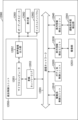
- FIG. 6 is a block diagram showing an example of the configuration of the imaging device 1 when the imaging device 1 is composed of the first to fourth semiconductors as in the second to fifth embodiments described above. be.
- the first semiconductor 11 includes a pixel array section 251 in which a plurality of pixels in which photodiodes 22 and the like are formed are arranged in a matrix, and pad sections 252A and 252B.
- the pad sections 252A and 252B are composed of a plurality of pads 34 shown in FIG. 1, and correspond to the input/output section of the imaging device 1.
- the pad section 252A includes a plurality of pads 34 electrically connected to the second semiconductor 12, and the pad section 252B includes a plurality of pads 34 electrically connected to the fourth semiconductor 101.
- the second semiconductor 12 includes at least a conversion circuit 81.
- the conversion circuit 81 converts the electrical characteristics or physical characteristics between the first semiconductor 11 and the third semiconductor 13, and also converts the electrical characteristics or physical characteristics between the third semiconductor 13 and the fourth semiconductor 101. By providing the second semiconductor 12 that includes at least the conversion circuit 81, compatibility with the third semiconductor 13 to be bonded can be improved.
- the third semiconductor 13 has a memory circuit 261 composed of, for example, a frame memory.
- the memory circuit 261 stores data supplied from the logic circuit 272 of the fourth semiconductor 101 via the conversion circuit 81.
- the fourth semiconductor 101 includes an analog/AD conversion circuit 271, a logic circuit 272, and an IF circuit 273.
- the analog/AD conversion circuit 271 includes an analog signal processing circuit that processes analog signals output from each pixel of the pixel array section 251, and an AD conversion circuit that converts the analog signal into a digital signal.
- the analog/AD conversion circuit 271 outputs a digitally converted (AD converted) signal to the logic circuit 272.
- the logic circuit 272 performs various digital signal processing, such as black level adjustment and column variation correction, on the signal supplied from the analog/AD conversion circuit 271.
- the logic circuit 272 outputs the processed signal to the IF circuit 273 or stores it in the memory circuit 261 of the third semiconductor 13 as necessary.
- the IF circuit 273 converts the signal supplied from the logic circuit 272 into a predetermined format, such as the MIPI (Mobile Industry Processor Interface) standard, and outputs it to an external device via the pad section 252B.
- MIPI Mobile Industry Processor Interface
- the third semiconductor 13 may be provided with the logic circuit 272, and the fourth semiconductor may be provided with the memory circuit 261.
- the memory circuit 261 and the logic circuit 272 may be provided in both the third semiconductor 13 and the fourth semiconductor.
- the logic circuit 272 includes a signal processing circuit that processes a signal generated by each pixel, and an AI processing circuit that performs AI processing based on the signal generated by each pixel.
- the conversion circuit 81 can include, for example, a parallel-to-serial conversion circuit.
- the parallel-serial conversion circuit is an example of a conversion circuit that converts electrical characteristics between the first semiconductor 11 and the third semiconductor 13.
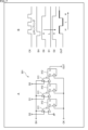
- FIG. 7 shows a specific configuration example and timing chart of the parallel-to-serial conversion circuit included in the conversion circuit 81.
- the parallel-serial conversion circuit 301 is composed of three selectors 311 and a D flip-flop 312, and converts three parallel signals D0, D1, D2 into serial signals and outputs the serial signals.
- Each selector 311 receives one of the parallel signals D0, D1, or D2 and an SH signal that controls sampling timing.
- Each selector 311 outputs the input B signal D0, D1, or D2 when the SH signal is Low.
- Each D flip-flop 312 stores the signal output from the selector 311 at the previous stage and supplied to the input D at the rising edge of the clock signal CK, and outputs it from the output Q.
- signals D0, D1, and D2 are sequentially output from the output OUT of the parallel-serial conversion circuit 301.
- the parallel-serial conversion circuit 301 can convert a low-speed parallel signal into a high-speed serial signal and output it.
- the conversion circuit 81 can include, for example, a serial-parallel conversion circuit.
- the serial-parallel conversion circuit is an example of a conversion circuit that converts electrical characteristics between the first semiconductor 11 and the third semiconductor 13.
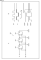
- FIG. 8 shows a specific configuration example and a timing chart of the serial-to-parallel conversion circuit included in the conversion circuit 81.
- the serial-parallel conversion circuit 321 is configured by connecting three D flip-flops 331, and converts the three signals D0, D1, D2 that are input sequentially into parallel signals and outputs the parallel signals.
- Each D flip-flop 331 stores the signal supplied to the input D at the rising edge of the clock signal CK, and outputs it from the output Q.
- signals D0, D1, and D2 are simultaneously output from the outputs OUT0, OUT1, and OUT2 of the serial-parallel conversion circuit 321.
- the serial-parallel conversion circuit 321 can convert a high-speed serial signal into a low-speed parallel signal and output it.
- the number of parallel semiconductor chips is determined by the number of pads of the semiconductor chips.
- the parallel-to-serial conversion circuit 301 or the serial-to-parallel conversion circuit 321 as at least part of the conversion circuit 81, the number of parallel data signals can be increased and the data rate can be increased.
- the wiring pitch of the third semiconductor 13 and the wiring pitch of the first semiconductor 11 may be different.
- the wiring pitch of the third semiconductor 13 using a general-purpose semiconductor chip is larger (wider) than the wiring pitch of the first semiconductor 11.
- the conversion circuit 81 may include a wiring pitch converter that converts the wiring pitch between the first semiconductor 11 and the third semiconductor 13.
- the wiring pitch conversion unit is an example of a conversion circuit that converts physical characteristics between the first semiconductor 11 and the third semiconductor 13.
- the conversion circuit 81 generates a clock signal CK for, for example, an arithmetic circuit that performs calculations on multiple images stored in the memory circuit 261, calculations on multiple pixels within an image, and the above-mentioned serial-to-parallel conversion circuit. It can include a logic circuit section such as a clock generation circuit.
- the logic circuit section is an example of a conversion circuit that converts electrical characteristics between the first semiconductor 11 and the third semiconductor 13. By providing the logic circuit section, the circuit area of the first semiconductor 11 can be reduced.
- the conversion circuit 81 can include, for example, a format conversion section.
- the format conversion unit is a circuit that converts the signal into a signal format compliant with standards such as DDR4, DDR5, and MIPI, and outputs the signal format.
- the format conversion unit is an example of a conversion circuit that converts electrical characteristics between the first semiconductor 11 and the third semiconductor 13. By providing the format conversion section, the signal format can be converted, and the degree of freedom in communication methods can be improved.
- the conversion circuit 81 can include, for example, a power supply section.
- the power supply section is, for example, a circuit that supplies the third semiconductor 13 with a power supply voltage input from the pad section 252A or 252B.
- the power supply unit is an example of a conversion circuit that converts electrical characteristics between the first semiconductor 11 and the third semiconductor 13.
- the conversion circuit 81 can include, for example, a test circuit that tests the operation of the third semiconductor 13.
- the test circuit is a circuit for testing the operation of these circuits.
- the test circuit is an example of a conversion circuit that converts electrical characteristics between the first semiconductor 11 and the third semiconductor 13.
- the imaging device 1 is configured by vertically stacking a first semiconductor 11, a second semiconductor 12, and a third semiconductor 13, and the second semiconductor is disposed between the first semiconductor 11 and the third semiconductor 13.
- 12 includes a conversion circuit 81 that converts electrical characteristics or physical characteristics.
- a general-purpose semiconductor chip can be used as the third semiconductor 13, and the manufacturing cost of the imaging device 1 can be reduced.
- the fourth semiconductor 101 is also bonded, a general-purpose semiconductor chip can be used for the fourth semiconductor 101 as well, and the manufacturing cost of the imaging device 1 can be further reduced.
- the first semiconductor 11 is formed to have a larger planar size than any of the second semiconductor 12, the third semiconductor 13, and the fourth semiconductor 101, and the second semiconductor 12 and the fourth semiconductor 101 are different from each other in the first semiconductor 11. Placed in a flat area.
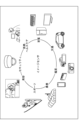
- FIG. 9 is a diagram showing an example of how an image sensor using the above-described imaging device 1 is used.
- the above-described imaging device 1 can be used as an image sensor in various cases for sensing light such as visible light, infrared light, ultraviolet light, and X-rays, for example, as described below.
- ⁇ Digital cameras, mobile devices with camera functions, and other devices that take images for viewing purposes Devices used for transportation, such as in-vehicle sensors that take pictures of the rear, surroundings, and interior of the car, surveillance cameras that monitor moving vehicles and roads, and distance sensors that measure the distance between vehicles, etc.
- Devices used for transportation such as in-vehicle sensors that take pictures of the rear, surroundings, and interior of the car, surveillance cameras that monitor moving vehicles and roads, and distance sensors that measure the distance between vehicles, etc.
- User gestures Devices used in home appliances such as TVs, refrigerators, and air conditioners to take pictures and operate devices according to the gestures.
- - Endoscopes devices that perform blood vessel imaging by receiving infrared light, etc.
- Devices used for medical and healthcare purposes - Devices used for security, such as surveillance cameras for crime prevention and cameras for person authentication - Skin measurement devices that take pictures of the skin, and devices that take pictures of the scalp - Devices used for beauty purposes, such as microscopes for skin care.
- - Devices used for sports such as action cameras and wearable cameras.
- - Cameras, etc. used to monitor the condition of fields and crops. , equipment used for agricultural purposes
- the present technology is not limited to application to imaging devices. In other words, this technology applies to imaging devices such as digital still cameras and video cameras, mobile terminal devices with an imaging function, and copying machines that use an imaging device in the image reading section. It is applicable to all electronic equipment using the device.
- the imaging device may be formed as a single chip, or may be a module having an imaging function in which an imaging section and a signal processing section or an optical system are packaged together.
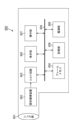
- FIG. 10 is a block diagram showing a configuration example of an electronic device to which the present technology is applied.
- the electronic device 600 in FIG. 10 includes an optical section 601 consisting of a lens group, etc., a solid-state imaging device (imaging device) 602 in which the configuration of the imaging device 1 in FIG. 1 is adopted, and a DSP (Digital Signal Processor) that is a camera signal processing circuit. ) circuit 603.
- the electronic device 600 also includes a frame memory 604, a display section 605, a recording section 606, an operation section 607, and a power supply section 608.
- the DSP circuit 603, frame memory 604, display section 605, recording section 606, operation section 607, and power supply section 608 are interconnected via a bus line 609.
- the optical section 601 takes in incident light (image light) from a subject and forms an image on the imaging surface of the solid-state imaging device 602.
- the solid-state imaging device 602 converts the amount of incident light that is imaged on the imaging surface by the optical unit 601 into an electrical signal for each pixel, and outputs the electric signal as a pixel signal.
- the imaging device 1 of FIG. It is possible to use an imaging device in which a conversion circuit 81 is provided in a second semiconductor 12 which is configured by bonding and is arranged between a first semiconductor 11 and a third semiconductor 13.
- the display unit 605 is configured with a thin display such as an LCD (Liquid Crystal Display) or an organic EL (Electro Luminescence) display, and displays moving images or still images captured by the solid-state imaging device 602.
- the recording unit 606 records a moving image or a still image captured by the solid-state imaging device 602 on a recording medium such as a hard disk or a semiconductor memory.
- the operation unit 607 issues operation commands regarding various functions of the electronic device 600 under operation by the user.
- a power supply unit 608 appropriately supplies various power supplies that serve as operating power for the DSP circuit 603, frame memory 604, display unit 605, recording unit 606, and operation unit 607 to these supply targets.
- manufacturing costs can be reduced and yield can be improved. Therefore, manufacturing costs can be reduced and yields can be improved in electronic devices 600 such as video cameras, digital still cameras, and even camera modules for mobile devices such as mobile phones.
- the technology according to the present disclosure (this technology) can be applied to various products.
- the technology according to the present disclosure may be realized as a device mounted on any type of moving body such as a car, electric vehicle, hybrid electric vehicle, motorcycle, bicycle, personal mobility, airplane, drone, ship, robot, etc. It's okay.
- FIG. 11 is a block diagram illustrating a schematic configuration example of a vehicle control system, which is an example of a mobile body control system to which the technology according to the present disclosure can be applied.
- the vehicle control system 12000 includes a plurality of electronic control units connected via a communication network 12001.
- the vehicle control system 12000 includes a drive system control unit 12010, a body system control unit 12020, an outside vehicle information detection unit 12030, an inside vehicle information detection unit 12040, and an integrated control unit 12050.
- a microcomputer 12051, an audio/image output section 12052, and an in-vehicle network I/F (interface) 12053 are illustrated.
- the drive system control unit 12010 controls the operation of devices related to the drive system of the vehicle according to various programs.
- the drive system control unit 12010 includes a drive force generation device such as an internal combustion engine or a drive motor that generates drive force for the vehicle, a drive force transmission mechanism that transmits the drive force to wheels, and a drive force transmission mechanism that controls the steering angle of the vehicle. It functions as a control device for a steering mechanism to adjust and a braking device to generate braking force for the vehicle.
- the body system control unit 12020 controls the operations of various devices installed in the vehicle body according to various programs.
- the body system control unit 12020 functions as a keyless entry system, a smart key system, a power window device, or a control device for various lamps such as a headlamp, a back lamp, a brake lamp, a turn signal, or a fog lamp.
- radio waves transmitted from a portable device that replaces a key or signals from various switches may be input to the body control unit 12020.
- the body system control unit 12020 receives input of these radio waves or signals, and controls the door lock device, power window device, lamp, etc. of the vehicle.
- the external information detection unit 12030 detects information external to the vehicle in which the vehicle control system 12000 is mounted.
- an imaging section 12031 is connected to the outside-vehicle information detection unit 12030.
- the vehicle exterior information detection unit 12030 causes the imaging unit 12031 to capture an image of the exterior of the vehicle, and receives the captured image.
- the external information detection unit 12030 may perform object detection processing such as a person, car, obstacle, sign, or text on the road surface or distance detection processing based on the received image.
- the imaging unit 12031 is an optical sensor that receives light and outputs an electrical signal according to the amount of received light.
- the imaging unit 12031 can output the electrical signal as an image or as distance measurement information.
- the light received by the imaging unit 12031 may be visible light or non-visible light such as infrared rays.
- the in-vehicle information detection unit 12040 detects in-vehicle information.
- a driver condition detection section 12041 that detects the condition of the driver is connected to the in-vehicle information detection unit 12040.
- the driver condition detection unit 12041 includes, for example, a camera that images the driver, and the in-vehicle information detection unit 12040 detects the degree of fatigue or concentration of the driver based on the detection information input from the driver condition detection unit 12041. It may be calculated, or it may be determined whether the driver is falling asleep.
- the microcomputer 12051 calculates control target values for the driving force generation device, steering mechanism, or braking device based on the information inside and outside the vehicle acquired by the vehicle exterior information detection unit 12030 or the vehicle interior information detection unit 12040, Control commands can be output to 12010.
- the microcomputer 12051 realizes ADAS (Advanced Driver Assistance System) functions, including vehicle collision avoidance or impact mitigation, following distance based on vehicle distance, vehicle speed maintenance, vehicle collision warning, vehicle lane departure warning, etc. It is possible to perform cooperative control for the purpose of ADAS (Advanced Driver Assistance System) functions, including vehicle collision avoidance or impact mitigation, following distance based on vehicle distance, vehicle speed maintenance, vehicle collision warning, vehicle lane departure warning, etc. It is possible to perform cooperative control for the purpose of
- ADAS Advanced Driver Assistance System
- the microcomputer 12051 controls the driving force generating device, steering mechanism, braking device, etc. based on information about the surroundings of the vehicle acquired by the vehicle exterior information detection unit 12030 or the vehicle interior information detection unit 12040. It is possible to perform cooperative control for the purpose of autonomous driving, etc., which does not rely on operation.
- the microcomputer 12051 can output a control command to the body system control unit 12020 based on the information outside the vehicle acquired by the outside information detection unit 12030.
- the microcomputer 12051 controls the headlamps according to the position of the preceding vehicle or oncoming vehicle detected by the vehicle exterior information detection unit 12030, and performs cooperative control for the purpose of preventing glare, such as switching from high beam to low beam. It can be carried out.
- the audio and image output unit 12052 transmits an output signal of at least one of audio and images to an output device that can visually or audibly notify information to the occupants of the vehicle or to the outside of the vehicle.
- an audio speaker 12061, a display section 12062, and an instrument panel 12063 are illustrated as output devices.
- the display unit 12062 may include, for example, at least one of an on-board display and a head-up display.
- FIG. 12 is a diagram showing an example of the installation position of the imaging section 12031.
- the vehicle 12100 has imaging units 12101, 12102, 12103, 12104, and 12105 as the imaging unit 12031.
- the imaging units 12101, 12102, 12103, 12104, and 12105 are provided, for example, at positions such as the front nose, side mirrors, rear bumper, back door, and the top of the windshield inside the vehicle 12100.
- An imaging unit 12101 provided in the front nose and an imaging unit 12105 provided above the windshield inside the vehicle mainly acquire images in front of the vehicle 12100.
- Imaging units 12102 and 12103 provided in the side mirrors mainly capture images of the sides of the vehicle 12100.
- An imaging unit 12104 provided in the rear bumper or back door mainly captures images of the rear of the vehicle 12100.
- the images of the front acquired by the imaging units 12101 and 12105 are mainly used for detecting preceding vehicles, pedestrians, obstacles, traffic lights, traffic signs, lanes, and the like.
- FIG. 12 shows an example of the imaging range of the imaging units 12101 to 12104.
- An imaging range 12111 indicates the imaging range of the imaging unit 12101 provided on the front nose
- imaging ranges 12112 and 12113 indicate imaging ranges of the imaging units 12102 and 12103 provided on the side mirrors, respectively
- an imaging range 12114 shows the imaging range of the imaging unit 12101 provided on the front nose.
- the imaging range of the imaging unit 12104 provided in the rear bumper or back door is shown. For example, by overlapping the image data captured by the imaging units 12101 to 12104, an overhead image of the vehicle 12100 viewed from above can be obtained.
- At least one of the imaging units 12101 to 12104 may have a function of acquiring distance information.
- at least one of the imaging units 12101 to 12104 may be a stereo camera including a plurality of image sensors, or may be an image sensor having pixels for phase difference detection.
- the microcomputer 12051 determines the distance to each three-dimensional object within the imaging ranges 12111 to 12114 and the temporal change in this distance (relative speed with respect to the vehicle 12100) based on the distance information obtained from the imaging units 12101 to 12104. In particular, by determining the three-dimensional object that is closest to the vehicle 12100 on its path and that is traveling at a predetermined speed (for example, 0 km/h or more) in approximately the same direction as the vehicle 12100, it is possible to extract the three-dimensional object as the preceding vehicle. can.
- a predetermined speed for example, 0 km/h or more
- the microcomputer 12051 can set an inter-vehicle distance to be secured in advance in front of the preceding vehicle, and perform automatic brake control (including follow-up stop control), automatic acceleration control (including follow-up start control), and the like. In this way, it is possible to perform cooperative control for the purpose of autonomous driving, etc., in which the vehicle travels autonomously without depending on the driver's operation.
- the microcomputer 12051 transfers three-dimensional object data to other three-dimensional objects such as two-wheeled vehicles, regular vehicles, large vehicles, pedestrians, and utility poles based on the distance information obtained from the imaging units 12101 to 12104. It can be classified and extracted and used for automatic obstacle avoidance. For example, the microcomputer 12051 identifies obstacles around the vehicle 12100 into obstacles that are visible to the driver of the vehicle 12100 and obstacles that are difficult to see. Then, the microcomputer 12051 determines a collision risk indicating the degree of risk of collision with each obstacle, and when the collision risk exceeds a set value and there is a possibility of a collision, the microcomputer 12051 transmits information via the audio speaker 12061 and the display unit 12062. By outputting a warning to the driver via the vehicle control unit 12010 and performing forced deceleration and avoidance steering via the drive system control unit 12010, driving support for collision avoidance can be provided.
- the microcomputer 12051 determines a collision risk indicating the degree of risk of collision with each obstacle, and when the collision risk exceed
- At least one of the imaging units 12101 to 12104 may be an infrared camera that detects infrared rays.
- the microcomputer 12051 can recognize a pedestrian by determining whether the pedestrian is present in the images captured by the imaging units 12101 to 12104.
- pedestrian recognition involves, for example, a procedure for extracting feature points in images captured by the imaging units 12101 to 12104 as infrared cameras, and a pattern matching process is performed on a series of feature points indicating the outline of an object to determine whether it is a pedestrian or not.
- the audio image output unit 12052 creates a rectangular outline for emphasis on the recognized pedestrian.
- the display unit 12062 is controlled to display the .
- the audio image output unit 12052 may control the display unit 12062 to display an icon or the like indicating a pedestrian at a desired position.
- the technology according to the present disclosure can be applied to the imaging unit 12031 among the configurations described above.
- the imaging device 1 according to each of the embodiments described above can be applied as the imaging unit 12031.
- the present disclosure is not limited to application to a solid-state imaging device that detects the distribution of the incident amount of visible light and captures the image as an image, but also applies to a solid-state imaging device that captures the distribution of the incident amount of infrared rays, X-rays, particles, etc. as an image. It can be applied to all solid-state imaging devices (physical quantity distribution detection devices) such as imaging devices and, in a broader sense, fingerprint detection sensors that detect the distribution of other physical quantities such as pressure and capacitance and capture the images as images. be.
- the present technology is applicable not only to solid-state imaging devices but also to all semiconductor devices having other semiconductor integrated circuits.
- a first semiconductor, a second semiconductor, and a third semiconductor are stacked in the vertical direction, The second semiconductor arranged between the first semiconductor and the third semiconductor includes a conversion circuit that converts electrical characteristics or physical characteristics.
- the semiconductor device according to (1) wherein a fourth semiconductor is further bonded to the first semiconductor in a plane region different from that of the second semiconductor.
- the semiconductor device according to (2) wherein the third semiconductor is connected to the fourth semiconductor via the conversion circuit of the second semiconductor and wiring of the first semiconductor.
- the first semiconductor is configured by stacking a plurality of semiconductor substrates, The semiconductor device according to (2) or (3), wherein the third semiconductor is connected to the fourth semiconductor via the conversion circuit of the second semiconductor and rewiring of the first semiconductor.
- the semiconductor device includes a wiring pitch conversion section that converts a wiring pitch.
- the conversion circuit includes a logic circuit section.
- the conversion circuit includes a format conversion section that converts a signal format.
- the conversion circuit includes a power supply section that supplies a power supply voltage to the third semiconductor.
- the conversion circuit includes a test circuit for the third semiconductor.
- the first semiconductor includes photoelectric conversion elements arranged in a matrix.
- the third semiconductor includes a logic circuit including a signal processing circuit or an AI processing circuit.
- the third semiconductor includes a memory circuit.
- a first semiconductor, a second semiconductor, and a third semiconductor are stacked in the vertical direction, The second semiconductor disposed between the first semiconductor and the third semiconductor includes a conversion circuit that converts electrical characteristics or physical characteristics.
- Imaging device 11 First semiconductor, 12 Second semiconductor, 13 Third semiconductor, 14 Support substrate, 15 Insulating layer, 16 Insulating film, 21 Semiconductor substrate, 22 Photodiode, 23 Planarizing film, 24 Color Filter, 25 on Chip lens, 31 metal wiring, 34 pad, 41 wiring layer, 51 semiconductor substrate, 61 semiconductor substrate, 81 conversion circuit, 82 area, 101 fourth semiconductor, 201 fifth semiconductor, 301 parallel-serial conversion circuit, 321 Serial-Parallel Conversion circuit, 600 Electronic equipment, 602 Solid-state imaging device
Landscapes
- Engineering & Computer Science (AREA)
- Multimedia (AREA)
- Signal Processing (AREA)
- Solid State Image Pick-Up Elements (AREA)
Abstract
Description
1.撮像装置の第1実施の形態
2.撮像装置の第2実施の形態
3.撮像装置の第3実施の形態
4.撮像装置の第4実施の形態
5.撮像装置の第5実施の形態
6.撮像装置のブロック図
7.変換回路の具体的構成例
8.まとめ
9.撮像装置の使用例
10.電子機器への適用例
11.移動体への応用例
図1は、本技術を適用した撮像装置の第1実施の形態の断面図を示している。
図2は、本技術を適用した撮像装置の第2実施の形態の断面図を示している。
図3は、本技術を適用した撮像装置の第3実施の形態の断面図を示している。
図4は、本技術を適用した撮像装置の第4実施の形態の断面図を示している。
図5は、本技術を適用した撮像装置の第5実施の形態の断面図を示している。
図6は、上述した第2実施の形態ないし第5実施の形態のように、撮像装置1が第1半導体ないし第4半導体で構成される場合の、撮像装置1の構成例を示すブロック図である。
次に、第2半導体12に設けられる変換回路81の具体的構成例について説明する。
変換回路81には、例えば、パラレル-シリアル変換回路を含むことができる。パラレル-シリアル変換回路は、第1半導体11と第3半導体13との間で電気特性を変換する変換回路の一例である。
変換回路81には、例えば、シリアル-パラレル変換回路を含むことができる。シリアル-パラレル変換回路は、第1半導体11と第3半導体13との間で電気特性を変換する変換回路の一例である。
例えば、メモリ回路261(図6)が形成された第3半導体13として汎用の半導体チップを用いた場合、第3半導体13の配線ピッチと、第1半導体11の配線ピッチとが異なることが考えられる。例えば、汎用の半導体チップを用いた第3半導体13の配線ピッチは、第1半導体11の配線ピッチよりも大きく(広く)なっている。変換回路81には、第1半導体11と第3半導体13との間で、配線ピッチを変換する配線ピッチ変換部を含む構成とすることができる。配線ピッチ変換部は、第1半導体11と第3半導体13との間で物理特性を変換する変換回路の一例である。配線ピッチ変換部を設けることにより、接合される第3半導体13との互換性を向上させることができる。
変換回路81には、例えば、メモリ回路261に記憶された複数の画像の演算や、画像内の複数画素の演算などを行う演算回路、上述したシリアル-パラレル変換回路等のクロック信号CKを生成するクロック生成回路などのロジック回路部を含むことができる。ロジック回路部は、第1半導体11と第3半導体13との間で電気特性を変換する変換回路の一例である。ロジック回路部を設けることにより、第1半導体11の回路面積を減らすことができる。
変換回路81には、例えば、フォーマット変換部を含むことができる。フォーマット変換部は、例えば、DDR4、DDR5、MIPIなどの規格に準拠した信号フォーマットに変換して出力する回路である。フォーマット変換部は、第1半導体11と第3半導体13との間で電気特性を変換する変換回路の一例である。フォーマット変換部を設けることにより、信号フォーマットを変換することができ、通信方式の自由度を向上させることができる。
変換回路81には、例えば、電源供給部を含むことができる。電源供給部は、例えば、パッド部252Aまたは252Bから入力された電源電圧を、第3半導体13へ供給する回路である。電源供給部は、第1半導体11と第3半導体13との間で電気特性を変換する変換回路の一例である。
変換回路81には、例えば、第3半導体13の動作をテストするテスト回路を含むことができる。テスト回路は、例えば、第3半導体13にアナログ/AD変換回路271やロジック回路272が設けられた場合、それらの回路の動作をテストするための回路である。テスト回路は、第1半導体11と第3半導体13との間で電気特性を変換する変換回路の一例である。
撮像装置1は、第1半導体11、第2半導体12、及び、第3半導体13が上下方向に積層して構成され、第1半導体11と第3半導体13との間に配置された第2半導体12が、電気特性または物理特性を変換する変換回路81を含む構成とされている。第2半導体12に変換回路81を設けたことにより、第3半導体13として汎用の半導体チップを採用することができ、撮像装置1の製造コストを低減することができる。第4半導体101も接合されている場合には、第4半導体101についても汎用の半導体チップを採用することができ、撮像装置1の製造コストをさらに低減することができる。第1半導体11は、第2半導体12、第3半導体13、及び、第4半導体101のどれよりも大きい平面サイズで形成され、第2半導体12と第4半導体101は、第1半導体11の異なる平面領域に配置される。
図9は、上述の撮像装置1を用いたイメージセンサの使用例を示す図である。
・自動停止等の安全運転や、運転者の状態の認識等のために、自動車の前方や後方、周囲、車内等を撮影する車載用センサ、走行車両や道路を監視する監視カメラ、車両間等の測距を行う測距センサ等の、交通の用に供される装置
・ユーザのジェスチャを撮影して、そのジェスチャに従った機器操作を行うために、TVや、冷蔵庫、エアーコンディショナ等の家電に供される装置
・内視鏡や、赤外光の受光による血管撮影を行う装置等の、医療やヘルスケアの用に供される装置
・防犯用途の監視カメラや、人物認証用途のカメラ等の、セキュリティの用に供される装置
・肌を撮影する肌測定器や、頭皮を撮影するマイクロスコープ等の、美容の用に供される装置
・スポーツ用途等向けのアクションカメラやウェアラブルカメラ等の、スポーツの用に供される装置
・畑や作物の状態を監視するためのカメラ等の、農業の用に供される装置
本技術は、撮像装置への適用に限られるものではない。即ち、本技術は、デジタルスチルカメラやビデオカメラ等の撮像装置や、撮像機能を有する携帯端末装置や、画像読取部に撮像装置を用いる複写機など、画像取込部(光電変換素子)に撮像装置を用いる電子機器全般に対して適用可能である。撮像装置は、ワンチップとして形成された形態であってもよいし、撮像部と信号処理部または光学系とがまとめてパッケージングされた撮像機能を有するモジュール形態であってもよい。
本開示に係る技術(本技術)は、様々な製品へ応用することができる。例えば、本開示に係る技術は、自動車、電気自動車、ハイブリッド電気自動車、自動二輪車、自転車、パーソナルモビリティ、飛行機、ドローン、船舶、ロボット等のいずれかの種類の移動体に搭載される装置として実現されてもよい。
(1)
第1半導体、第2半導体、及び、第3半導体が上下方向に積層して構成され、
前記第1半導体と前記第3半導体との間に配置された前記第2半導体は、電気特性または物理特性を変換する変換回路を含む
半導体装置。
(2)
前記第1半導体には、前記第2半導体と異なる平面領域に、第4半導体がさらに接合されて構成されている
前記(1)に記載の半導体装置。
(3)
前記第3半導体は、前記第2半導体の前記変換回路と、前記第1半導体の配線を介して、前記第4半導体と接続されている
前記(2)に記載の半導体装置。
(4)
前記第1半導体は、複数の半導体基板を積層して構成され、
前記第3半導体は、前記第2半導体の前記変換回路と、前記第1半導体の再配線を介して、前記第4半導体と接続されている
前記(2)または(3)に記載の半導体装置。
(5)
前記第4半導体は、前記第2半導体と前記第3半導体を積層した厚みと異なる厚みを有する
前記(2)ないし(4)のいずれかに記載の半導体装置。
(6)
前記第4半導体は、前記第2半導体と前記第3半導体を積層した厚みと同じ厚みを有する
前記(2)ないし(4)のいずれかに記載の半導体装置。
(7)
前記第4半導体とダミー基板とを合わせた厚みが、前記第2半導体と前記第3半導体を積層した厚みと同じ厚みに構成されている
前記(6)に記載の半導体装置。
(8)
前記変換回路は、パラレル-シリアル変換回路を含む
前記(1)ないし(7)のいずれかに記載の半導体装置。
(9)
前記変換回路は、シリアル-パラレル変換回路を含む
前記(1)ないし(8)のいずれかに記載の半導体装置。
(10)
前記変換回路は、配線ピッチを変換する配線ピッチ変換部を含む
前記(1)ないし(9)のいずれかに記載の半導体装置。
(11)
前記変換回路は、ロジック回路部を含む
前記(1)ないし(10)のいずれかに記載の半導体装置。
(12)
前記変換回路は、信号フォーマットを変換するフォーマット変換部を含む
前記(1)ないし(11)のいずれかに記載の半導体装置。
(13)
前記変換回路は、前記第3半導体へ電源電圧を供給する電源供給部を含む
前記(1)ないし(12)のいずれかに記載の半導体装置。
(14)
前記変換回路は、前記第3半導体のテスト回路を含む
前記(1)ないし(13)のいずれかに記載の半導体装置。
(15)
前記第1半導体は、前記第2半導体及び前記第3半導体よりも大きい平面サイズを有する
前記(1)ないし(14)のいずれかに記載の半導体装置。
(16)
前記第1半導体は、行列状に配列された光電変換素子を含む
前記(1)ないし(15)のいずれかに記載の半導体装置。
(17)
前記第3半導体は、信号処理回路またはAI処理回路を含むロジック回路を含む
前記(1)ないし(16)のいずれかに記載の半導体装置。
(18)
前記第3半導体は、メモリ回路を含む
前記(1)ないし(17)のいずれかに記載の半導体装置。
(19)
第1半導体、第2半導体、及び、第3半導体が上下方向に積層して構成され、
前記第1半導体と前記第3半導体との間に配置された前記第2半導体は、電気特性または物理特性を変換する変換回路を含む
半導体装置
を備える電子機器。
Claims (19)
- 第1半導体、第2半導体、及び、第3半導体が上下方向に積層して構成され、
前記第1半導体と前記第3半導体との間に配置された前記第2半導体は、電気特性または物理特性を変換する変換回路を含む
半導体装置。 - 前記第1半導体には、前記第2半導体と異なる平面領域に、第4半導体がさらに接合されて構成されている
請求項1に記載の半導体装置。 - 前記第3半導体は、前記第2半導体の前記変換回路と、前記第1半導体の配線を介して、前記第4半導体と接続されている
請求項2に記載の半導体装置。 - 前記第1半導体は、複数の半導体基板を積層して構成され、
前記第3半導体は、前記第2半導体の前記変換回路と、前記第1半導体の再配線を介して、前記第4半導体と接続されている
請求項2に記載の半導体装置。 - 前記第4半導体は、前記第2半導体と前記第3半導体を積層した厚みと異なる厚みを有する
請求項2に記載の半導体装置。 - 前記第4半導体は、前記第2半導体と前記第3半導体を積層した厚みと同じ厚みを有する
請求項2に記載の半導体装置。 - 前記第4半導体とダミー基板とを合わせた厚みが、前記第2半導体と前記第3半導体を積層した厚みと同じ厚みに構成されている
請求項6に記載の半導体装置。 - 前記変換回路は、パラレル-シリアル変換回路を含む
請求項1に記載の半導体装置。 - 前記変換回路は、シリアル-パラレル変換回路を含む
請求項1に記載の半導体装置。 - 前記変換回路は、配線ピッチを変換する配線ピッチ変換部を含む
請求項1に記載の半導体装置。 - 前記変換回路は、ロジック回路部を含む
請求項1に記載の半導体装置。 - 前記変換回路は、信号フォーマットを変換するフォーマット変換部を含む
請求項1に記載の半導体装置。 - 前記変換回路は、前記第3半導体へ電源電圧を供給する電源供給部を含む
請求項1に記載の半導体装置。 - 前記変換回路は、前記第3半導体のテスト回路を含む
請求項1に記載の半導体装置。 - 前記第1半導体は、前記第2半導体及び前記第3半導体よりも大きい平面サイズを有する
請求項1に記載の半導体装置。 - 前記第1半導体は、行列状に配列された光電変換素子を含む
請求項1に記載の半導体装置。 - 前記第3半導体は、信号処理回路またはAI処理回路を含むロジック回路を含む
請求項1に記載の半導体装置。 - 前記第3半導体は、メモリ回路を含む
請求項1に記載の半導体装置。 - 第1半導体、第2半導体、及び、第3半導体が上下方向に積層して構成され、
前記第1半導体と前記第3半導体との間に配置された前記第2半導体は、電気特性または物理特性を変換する変換回路を含む
半導体装置
を備える電子機器。
Priority Applications (2)
| Application Number | Priority Date | Filing Date | Title |
|---|---|---|---|
| US18/995,046 US20260026125A1 (en) | 2022-08-17 | 2023-08-01 | Semiconductor device and electronic apparatus |
| CN202380051738.8A CN119522645A (zh) | 2022-08-17 | 2023-08-01 | 半导体装置和电子设备 |
Applications Claiming Priority (2)
| Application Number | Priority Date | Filing Date | Title |
|---|---|---|---|
| JP2022-129910 | 2022-08-17 | ||
| JP2022129910 | 2022-08-17 |
Publications (1)
| Publication Number | Publication Date |
|---|---|
| WO2024038757A1 true WO2024038757A1 (ja) | 2024-02-22 |
Family
ID=89941559
Family Applications (1)
| Application Number | Title | Priority Date | Filing Date |
|---|---|---|---|
| PCT/JP2023/028064 Ceased WO2024038757A1 (ja) | 2022-08-17 | 2023-08-01 | 半導体装置および電子機器 |
Country Status (3)
| Country | Link |
|---|---|
| US (1) | US20260026125A1 (ja) |
| CN (1) | CN119522645A (ja) |
| WO (1) | WO2024038757A1 (ja) |
Citations (5)
| Publication number | Priority date | Publication date | Assignee | Title |
|---|---|---|---|---|
| JP2015126043A (ja) * | 2013-12-26 | 2015-07-06 | ソニー株式会社 | 電子デバイス |
| WO2018173764A1 (ja) * | 2017-03-21 | 2018-09-27 | 富士フイルム株式会社 | 積層デバイス、積層体および積層デバイスの製造方法 |
| JP2018181988A (ja) * | 2017-04-10 | 2018-11-15 | ブリルニクスジャパン株式会社 | 固体撮像装置、固体撮像装置の製造方法、および電子機器 |
| JP2020072410A (ja) * | 2018-10-31 | 2020-05-07 | ソニーセミコンダクタソリューションズ株式会社 | 固体撮像装置及び電子機器 |
| JP2022074493A (ja) * | 2020-11-04 | 2022-05-18 | ソニーセミコンダクタソリューションズ株式会社 | 固体撮像装置および電子機器 |
-
2023
- 2023-08-01 US US18/995,046 patent/US20260026125A1/en active Pending
- 2023-08-01 CN CN202380051738.8A patent/CN119522645A/zh active Pending
- 2023-08-01 WO PCT/JP2023/028064 patent/WO2024038757A1/ja not_active Ceased
Patent Citations (5)
| Publication number | Priority date | Publication date | Assignee | Title |
|---|---|---|---|---|
| JP2015126043A (ja) * | 2013-12-26 | 2015-07-06 | ソニー株式会社 | 電子デバイス |
| WO2018173764A1 (ja) * | 2017-03-21 | 2018-09-27 | 富士フイルム株式会社 | 積層デバイス、積層体および積層デバイスの製造方法 |
| JP2018181988A (ja) * | 2017-04-10 | 2018-11-15 | ブリルニクスジャパン株式会社 | 固体撮像装置、固体撮像装置の製造方法、および電子機器 |
| JP2020072410A (ja) * | 2018-10-31 | 2020-05-07 | ソニーセミコンダクタソリューションズ株式会社 | 固体撮像装置及び電子機器 |
| JP2022074493A (ja) * | 2020-11-04 | 2022-05-18 | ソニーセミコンダクタソリューションズ株式会社 | 固体撮像装置および電子機器 |
Also Published As
| Publication number | Publication date |
|---|---|
| US20260026125A1 (en) | 2026-01-22 |
| CN119522645A (zh) | 2025-02-25 |
Similar Documents
| Publication | Publication Date | Title |
|---|---|---|
| KR102246424B1 (ko) | 촬상 장치 및 촬상 방법, 카메라 모듈, 및 전자 기기 | |
| US12349487B2 (en) | Solid-state image pickup device and electronic apparatus | |
| WO2022196188A1 (ja) | 撮像装置、撮像装置の製造方法、および電子機器 | |
| US12191337B2 (en) | Imaging unit, method for manufacturing the same, and electronic apparatus | |
| EP4471847A1 (en) | Semiconductor device, method for manufacturing same, and electronic apparatus | |
| US20240222410A1 (en) | Solid-state imaging apparatus, manufacturing method thereof, and electronic equipment | |
| CN111886855B (zh) | 摄像装置和电子设备 | |
| JP7654551B2 (ja) | 撮像装置、電子機器、製造方法 | |
| JP7785776B2 (ja) | 固体撮像素子、撮像装置、および電子機器 | |
| WO2024038757A1 (ja) | 半導体装置および電子機器 | |
| CN114008783A (zh) | 摄像装置 | |
| JP7630428B2 (ja) | 半導体パッケージ | |
| WO2023210324A1 (ja) | 固体撮像装置および電子機器 | |
| WO2024084865A1 (ja) | 半導体装置 | |
| WO2023248606A1 (ja) | パッケージ、半導体装置およびパッケージの製造方法 | |
| US20250351610A1 (en) | Semiconductor device and imaging device | |
| WO2024241891A1 (ja) | 固体撮像装置および電子機器 | |
| WO2025062845A1 (ja) | 光検出装置、電子機器及び光検出装置の製造方法 | |
| WO2024195725A1 (ja) | 半導体装置 | |
| WO2024157747A1 (ja) | 固体撮像装置 | |
| JP2025123863A (ja) | 半導体素子 | |
| WO2024111248A1 (ja) | 半導体パッケージ、光学装置、および、半導体パッケージの製造方法 | |
| WO2018155195A1 (ja) | 撮像装置、電子機器、及び、撮像装置の製造方法 |
Legal Events
| Date | Code | Title | Description |
|---|---|---|---|
| 121 | Ep: the epo has been informed by wipo that ep was designated in this application |
Ref document number: 23854792 Country of ref document: EP Kind code of ref document: A1 |
|
| WWE | Wipo information: entry into national phase |
Ref document number: 202380051738.8 Country of ref document: CN |
|
| WWE | Wipo information: entry into national phase |
Ref document number: 18995046 Country of ref document: US |
|
| WWP | Wipo information: published in national office |
Ref document number: 202380051738.8 Country of ref document: CN |
|
| NENP | Non-entry into the national phase |
Ref country code: DE |
|
| 122 | Ep: pct application non-entry in european phase |
Ref document number: 23854792 Country of ref document: EP Kind code of ref document: A1 |
|
| NENP | Non-entry into the national phase |
Ref country code: JP |
|
| WWP | Wipo information: published in national office |
Ref document number: 18995046 Country of ref document: US |