WO2024029577A1 - Electrochemical element - Google Patents
Electrochemical element Download PDFInfo
- Publication number
- WO2024029577A1 WO2024029577A1 PCT/JP2023/028322 JP2023028322W WO2024029577A1 WO 2024029577 A1 WO2024029577 A1 WO 2024029577A1 JP 2023028322 W JP2023028322 W JP 2023028322W WO 2024029577 A1 WO2024029577 A1 WO 2024029577A1
- Authority
- WO
- WIPO (PCT)
- Prior art keywords
- electrode layer
- conductive plate
- spring
- power generation
- electrochemical
- Prior art date
Links
- 238000010248 power generation Methods 0.000 claims abstract description 97
- 239000000463 material Substances 0.000 claims description 43
- 229910052751 metal Inorganic materials 0.000 claims description 34
- 239000002184 metal Substances 0.000 claims description 34
- 238000003825 pressing Methods 0.000 claims description 23
- 238000002955 isolation Methods 0.000 claims description 6
- 230000000630 rising effect Effects 0.000 claims description 3
- 238000007789 sealing Methods 0.000 abstract description 28
- 239000007784 solid electrolyte Substances 0.000 abstract description 24
- 230000002349 favourable effect Effects 0.000 abstract 1
- 238000012986 modification Methods 0.000 description 42
- 230000004048 modification Effects 0.000 description 42
- OKTJSMMVPCPJKN-UHFFFAOYSA-N Carbon Chemical compound [C] OKTJSMMVPCPJKN-UHFFFAOYSA-N 0.000 description 32
- 229910002804 graphite Inorganic materials 0.000 description 27
- 239000010439 graphite Substances 0.000 description 27
- 239000004020 conductor Substances 0.000 description 21
- 230000002093 peripheral effect Effects 0.000 description 13
- 238000004519 manufacturing process Methods 0.000 description 10
- 238000000034 method Methods 0.000 description 9
- HBBGRARXTFLTSG-UHFFFAOYSA-N Lithium ion Chemical compound [Li+] HBBGRARXTFLTSG-UHFFFAOYSA-N 0.000 description 8
- 229910001416 lithium ion Inorganic materials 0.000 description 8
- 239000011347 resin Substances 0.000 description 7
- 229920005989 resin Polymers 0.000 description 7
- WHXSMMKQMYFTQS-UHFFFAOYSA-N Lithium Chemical compound [Li] WHXSMMKQMYFTQS-UHFFFAOYSA-N 0.000 description 6
- UCKMPCXJQFINFW-UHFFFAOYSA-N Sulphide Chemical compound [S-2] UCKMPCXJQFINFW-UHFFFAOYSA-N 0.000 description 6
- 239000002253 acid Substances 0.000 description 6
- 239000003990 capacitor Substances 0.000 description 6
- 229910052744 lithium Inorganic materials 0.000 description 6
- 239000000203 mixture Substances 0.000 description 6
- 238000012360 testing method Methods 0.000 description 5
- 238000005452 bending Methods 0.000 description 4
- 239000000919 ceramic Substances 0.000 description 4
- 230000000694 effects Effects 0.000 description 4
- 239000007774 positive electrode material Substances 0.000 description 4
- 230000001133 acceleration Effects 0.000 description 3
- 229910052799 carbon Inorganic materials 0.000 description 3
- 238000005520 cutting process Methods 0.000 description 3
- 230000007423 decrease Effects 0.000 description 3
- 239000011521 glass Substances 0.000 description 3
- 239000001307 helium Substances 0.000 description 3
- 229910052734 helium Inorganic materials 0.000 description 3
- SWQJXJOGLNCZEY-UHFFFAOYSA-N helium atom Chemical compound [He] SWQJXJOGLNCZEY-UHFFFAOYSA-N 0.000 description 3
- 239000007769 metal material Substances 0.000 description 3
- 238000003466 welding Methods 0.000 description 3
- IJGRMHOSHXDMSA-UHFFFAOYSA-N Atomic nitrogen Chemical compound N#N IJGRMHOSHXDMSA-UHFFFAOYSA-N 0.000 description 2
- XEEYBQQBJWHFJM-UHFFFAOYSA-N Iron Chemical compound [Fe] XEEYBQQBJWHFJM-UHFFFAOYSA-N 0.000 description 2
- PXHVJJICTQNCMI-UHFFFAOYSA-N Nickel Chemical compound [Ni] PXHVJJICTQNCMI-UHFFFAOYSA-N 0.000 description 2
- RTAQQCXQSZGOHL-UHFFFAOYSA-N Titanium Chemical compound [Ti] RTAQQCXQSZGOHL-UHFFFAOYSA-N 0.000 description 2
- 239000000853 adhesive Substances 0.000 description 2
- 230000001070 adhesive effect Effects 0.000 description 2
- 238000006243 chemical reaction Methods 0.000 description 2
- 239000002131 composite material Substances 0.000 description 2
- 239000000470 constituent Substances 0.000 description 2
- 238000006073 displacement reaction Methods 0.000 description 2
- 238000011156 evaluation Methods 0.000 description 2
- 239000007789 gas Substances 0.000 description 2
- 229910021389 graphene Inorganic materials 0.000 description 2
- 239000007773 negative electrode material Substances 0.000 description 2
- 239000008188 pellet Substances 0.000 description 2
- 238000007639 printing Methods 0.000 description 2
- 238000000926 separation method Methods 0.000 description 2
- 238000009751 slip forming Methods 0.000 description 2
- 239000010935 stainless steel Substances 0.000 description 2
- 229910001220 stainless steel Inorganic materials 0.000 description 2
- 238000003860 storage Methods 0.000 description 2
- 239000010936 titanium Substances 0.000 description 2
- VYZAMTAEIAYCRO-UHFFFAOYSA-N Chromium Chemical compound [Cr] VYZAMTAEIAYCRO-UHFFFAOYSA-N 0.000 description 1
- RYGMFSIKBFXOCR-UHFFFAOYSA-N Copper Chemical compound [Cu] RYGMFSIKBFXOCR-UHFFFAOYSA-N 0.000 description 1
- 229910000733 Li alloy Inorganic materials 0.000 description 1
- 239000004734 Polyphenylene sulfide Substances 0.000 description 1
- 239000004743 Polypropylene Substances 0.000 description 1
- SOXUFMZTHZXOGC-UHFFFAOYSA-N [Li].[Mn].[Co].[Ni] Chemical compound [Li].[Mn].[Co].[Ni] SOXUFMZTHZXOGC-UHFFFAOYSA-N 0.000 description 1
- 238000004026 adhesive bonding Methods 0.000 description 1
- 239000000956 alloy Substances 0.000 description 1
- 229910045601 alloy Inorganic materials 0.000 description 1
- 229910052782 aluminium Inorganic materials 0.000 description 1
- XAGFODPZIPBFFR-UHFFFAOYSA-N aluminium Chemical compound [Al] XAGFODPZIPBFFR-UHFFFAOYSA-N 0.000 description 1
- 239000005388 borosilicate glass Substances 0.000 description 1
- 239000003795 chemical substances by application Substances 0.000 description 1
- 239000011651 chromium Substances 0.000 description 1
- 229910052804 chromium Inorganic materials 0.000 description 1
- 239000011248 coating agent Substances 0.000 description 1
- 238000000576 coating method Methods 0.000 description 1
- 239000010941 cobalt Substances 0.000 description 1
- 229910017052 cobalt Inorganic materials 0.000 description 1
- GUTLYIVDDKVIGB-UHFFFAOYSA-N cobalt atom Chemical compound [Co] GUTLYIVDDKVIGB-UHFFFAOYSA-N 0.000 description 1
- 230000006835 compression Effects 0.000 description 1
- 238000007906 compression Methods 0.000 description 1
- 239000006258 conductive agent Substances 0.000 description 1
- 229910052802 copper Inorganic materials 0.000 description 1
- 239000010949 copper Substances 0.000 description 1
- 239000013078 crystal Substances 0.000 description 1
- 238000011161 development Methods 0.000 description 1
- QHGJSLXSVXVKHZ-UHFFFAOYSA-N dilithium;dioxido(dioxo)manganese Chemical compound [Li+].[Li+].[O-][Mn]([O-])(=O)=O QHGJSLXSVXVKHZ-UHFFFAOYSA-N 0.000 description 1
- 239000003792 electrolyte Substances 0.000 description 1
- 239000008151 electrolyte solution Substances 0.000 description 1
- 239000006260 foam Substances 0.000 description 1
- 238000005187 foaming Methods 0.000 description 1
- 239000002241 glass-ceramic Substances 0.000 description 1
- 239000012943 hotmelt Substances 0.000 description 1
- 150000004678 hydrides Chemical class 0.000 description 1
- 239000011261 inert gas Substances 0.000 description 1
- 239000011810 insulating material Substances 0.000 description 1
- 238000009413 insulation Methods 0.000 description 1
- 229910052742 iron Inorganic materials 0.000 description 1
- 238000005304 joining Methods 0.000 description 1
- 239000001989 lithium alloy Substances 0.000 description 1
- 229910000625 lithium cobalt oxide Inorganic materials 0.000 description 1
- BFZPBUKRYWOWDV-UHFFFAOYSA-N lithium;oxido(oxo)cobalt Chemical compound [Li+].[O-][Co]=O BFZPBUKRYWOWDV-UHFFFAOYSA-N 0.000 description 1
- 150000002739 metals Chemical class 0.000 description 1
- 229910021382 natural graphite Inorganic materials 0.000 description 1
- 229910052759 nickel Inorganic materials 0.000 description 1
- 229910000484 niobium oxide Inorganic materials 0.000 description 1
- URLJKFSTXLNXLG-UHFFFAOYSA-N niobium(5+);oxygen(2-) Chemical compound [O-2].[O-2].[O-2].[O-2].[O-2].[Nb+5].[Nb+5] URLJKFSTXLNXLG-UHFFFAOYSA-N 0.000 description 1
- 229910052757 nitrogen Inorganic materials 0.000 description 1
- 239000011255 nonaqueous electrolyte Substances 0.000 description 1
- 239000002245 particle Substances 0.000 description 1
- 230000000149 penetrating effect Effects 0.000 description 1
- 229920006122 polyamide resin Polymers 0.000 description 1
- 229920000069 polyphenylene sulfide Polymers 0.000 description 1
- -1 polypropylene Polymers 0.000 description 1
- 229920001155 polypropylene Polymers 0.000 description 1
- 239000011148 porous material Substances 0.000 description 1
- 239000000843 powder Substances 0.000 description 1
- 230000001105 regulatory effect Effects 0.000 description 1
- 239000000565 sealant Substances 0.000 description 1
- 239000007787 solid Substances 0.000 description 1
- 238000010998 test method Methods 0.000 description 1
- 229910052719 titanium Inorganic materials 0.000 description 1
- 230000008016 vaporization Effects 0.000 description 1
Images


Classifications
-
- H—ELECTRICITY
- H01—ELECTRIC ELEMENTS
- H01M—PROCESSES OR MEANS, e.g. BATTERIES, FOR THE DIRECT CONVERSION OF CHEMICAL ENERGY INTO ELECTRICAL ENERGY
- H01M50/00—Constructional details or processes of manufacture of the non-active parts of electrochemical cells other than fuel cells, e.g. hybrid cells
- H01M50/50—Current conducting connections for cells or batteries
- H01M50/531—Electrode connections inside a battery casing
-
- H—ELECTRICITY
- H01—ELECTRIC ELEMENTS
- H01G—CAPACITORS; CAPACITORS, RECTIFIERS, DETECTORS, SWITCHING DEVICES, LIGHT-SENSITIVE OR TEMPERATURE-SENSITIVE DEVICES OF THE ELECTROLYTIC TYPE
- H01G11/00—Hybrid capacitors, i.e. capacitors having different positive and negative electrodes; Electric double-layer [EDL] capacitors; Processes for the manufacture thereof or of parts thereof
- H01G11/04—Hybrid capacitors
- H01G11/06—Hybrid capacitors with one of the electrodes allowing ions to be reversibly doped thereinto, e.g. lithium ion capacitors [LIC]
-
- H—ELECTRICITY
- H01—ELECTRIC ELEMENTS
- H01G—CAPACITORS; CAPACITORS, RECTIFIERS, DETECTORS, SWITCHING DEVICES, LIGHT-SENSITIVE OR TEMPERATURE-SENSITIVE DEVICES OF THE ELECTROLYTIC TYPE
- H01G11/00—Hybrid capacitors, i.e. capacitors having different positive and negative electrodes; Electric double-layer [EDL] capacitors; Processes for the manufacture thereof or of parts thereof
- H01G11/66—Current collectors
- H01G11/70—Current collectors characterised by their structure
-
- H—ELECTRICITY
- H01—ELECTRIC ELEMENTS
- H01G—CAPACITORS; CAPACITORS, RECTIFIERS, DETECTORS, SWITCHING DEVICES, LIGHT-SENSITIVE OR TEMPERATURE-SENSITIVE DEVICES OF THE ELECTROLYTIC TYPE
- H01G9/00—Electrolytic capacitors, rectifiers, detectors, switching devices, light-sensitive or temperature-sensitive devices; Processes of their manufacture
- H01G9/004—Details
- H01G9/08—Housing; Encapsulation
-
- H—ELECTRICITY
- H01—ELECTRIC ELEMENTS
- H01M—PROCESSES OR MEANS, e.g. BATTERIES, FOR THE DIRECT CONVERSION OF CHEMICAL ENERGY INTO ELECTRICAL ENERGY
- H01M10/00—Secondary cells; Manufacture thereof
- H01M10/04—Construction or manufacture in general
- H01M10/0481—Compression means other than compression means for stacks of electrodes and separators
-
- H—ELECTRICITY
- H01—ELECTRIC ELEMENTS
- H01M—PROCESSES OR MEANS, e.g. BATTERIES, FOR THE DIRECT CONVERSION OF CHEMICAL ENERGY INTO ELECTRICAL ENERGY
- H01M10/00—Secondary cells; Manufacture thereof
- H01M10/05—Accumulators with non-aqueous electrolyte
- H01M10/052—Li-accumulators
-
- H—ELECTRICITY
- H01—ELECTRIC ELEMENTS
- H01M—PROCESSES OR MEANS, e.g. BATTERIES, FOR THE DIRECT CONVERSION OF CHEMICAL ENERGY INTO ELECTRICAL ENERGY
- H01M10/00—Secondary cells; Manufacture thereof
- H01M10/05—Accumulators with non-aqueous electrolyte
- H01M10/058—Construction or manufacture
- H01M10/0585—Construction or manufacture of accumulators having only flat construction elements, i.e. flat positive electrodes, flat negative electrodes and flat separators
-
- H—ELECTRICITY
- H01—ELECTRIC ELEMENTS
- H01M—PROCESSES OR MEANS, e.g. BATTERIES, FOR THE DIRECT CONVERSION OF CHEMICAL ENERGY INTO ELECTRICAL ENERGY
- H01M50/00—Constructional details or processes of manufacture of the non-active parts of electrochemical cells other than fuel cells, e.g. hybrid cells
- H01M50/10—Primary casings; Jackets or wrappings
- H01M50/102—Primary casings; Jackets or wrappings characterised by their shape or physical structure
- H01M50/103—Primary casings; Jackets or wrappings characterised by their shape or physical structure prismatic or rectangular
-
- H—ELECTRICITY
- H01—ELECTRIC ELEMENTS
- H01M—PROCESSES OR MEANS, e.g. BATTERIES, FOR THE DIRECT CONVERSION OF CHEMICAL ENERGY INTO ELECTRICAL ENERGY
- H01M50/00—Constructional details or processes of manufacture of the non-active parts of electrochemical cells other than fuel cells, e.g. hybrid cells
- H01M50/10—Primary casings; Jackets or wrappings
- H01M50/102—Primary casings; Jackets or wrappings characterised by their shape or physical structure
- H01M50/109—Primary casings; Jackets or wrappings characterised by their shape or physical structure of button or coin shape
-
- H—ELECTRICITY
- H01—ELECTRIC ELEMENTS
- H01M—PROCESSES OR MEANS, e.g. BATTERIES, FOR THE DIRECT CONVERSION OF CHEMICAL ENERGY INTO ELECTRICAL ENERGY
- H01M50/00—Constructional details or processes of manufacture of the non-active parts of electrochemical cells other than fuel cells, e.g. hybrid cells
- H01M50/10—Primary casings; Jackets or wrappings
- H01M50/147—Lids or covers
- H01M50/148—Lids or covers characterised by their shape
- H01M50/15—Lids or covers characterised by their shape for prismatic or rectangular cells
-
- H—ELECTRICITY
- H01—ELECTRIC ELEMENTS
- H01M—PROCESSES OR MEANS, e.g. BATTERIES, FOR THE DIRECT CONVERSION OF CHEMICAL ENERGY INTO ELECTRICAL ENERGY
- H01M50/00—Constructional details or processes of manufacture of the non-active parts of electrochemical cells other than fuel cells, e.g. hybrid cells
- H01M50/10—Primary casings; Jackets or wrappings
- H01M50/147—Lids or covers
- H01M50/148—Lids or covers characterised by their shape
- H01M50/153—Lids or covers characterised by their shape for button or coin cells
-
- H—ELECTRICITY
- H01—ELECTRIC ELEMENTS
- H01M—PROCESSES OR MEANS, e.g. BATTERIES, FOR THE DIRECT CONVERSION OF CHEMICAL ENERGY INTO ELECTRICAL ENERGY
- H01M50/00—Constructional details or processes of manufacture of the non-active parts of electrochemical cells other than fuel cells, e.g. hybrid cells
- H01M50/10—Primary casings; Jackets or wrappings
- H01M50/172—Arrangements of electric connectors penetrating the casing
- H01M50/174—Arrangements of electric connectors penetrating the casing adapted for the shape of the cells
- H01M50/176—Arrangements of electric connectors penetrating the casing adapted for the shape of the cells for prismatic or rectangular cells
-
- H—ELECTRICITY
- H01—ELECTRIC ELEMENTS
- H01M—PROCESSES OR MEANS, e.g. BATTERIES, FOR THE DIRECT CONVERSION OF CHEMICAL ENERGY INTO ELECTRICAL ENERGY
- H01M50/00—Constructional details or processes of manufacture of the non-active parts of electrochemical cells other than fuel cells, e.g. hybrid cells
- H01M50/10—Primary casings; Jackets or wrappings
- H01M50/172—Arrangements of electric connectors penetrating the casing
- H01M50/174—Arrangements of electric connectors penetrating the casing adapted for the shape of the cells
- H01M50/181—Arrangements of electric connectors penetrating the casing adapted for the shape of the cells for button or coin cells
-
- H—ELECTRICITY
- H01—ELECTRIC ELEMENTS
- H01M—PROCESSES OR MEANS, e.g. BATTERIES, FOR THE DIRECT CONVERSION OF CHEMICAL ENERGY INTO ELECTRICAL ENERGY
- H01M50/00—Constructional details or processes of manufacture of the non-active parts of electrochemical cells other than fuel cells, e.g. hybrid cells
- H01M50/20—Mountings; Secondary casings or frames; Racks, modules or packs; Suspension devices; Shock absorbers; Transport or carrying devices; Holders
- H01M50/202—Casings or frames around the primary casing of a single cell or a single battery
-
- H—ELECTRICITY
- H01—ELECTRIC ELEMENTS
- H01M—PROCESSES OR MEANS, e.g. BATTERIES, FOR THE DIRECT CONVERSION OF CHEMICAL ENERGY INTO ELECTRICAL ENERGY
- H01M50/00—Constructional details or processes of manufacture of the non-active parts of electrochemical cells other than fuel cells, e.g. hybrid cells
- H01M50/20—Mountings; Secondary casings or frames; Racks, modules or packs; Suspension devices; Shock absorbers; Transport or carrying devices; Holders
- H01M50/289—Mountings; Secondary casings or frames; Racks, modules or packs; Suspension devices; Shock absorbers; Transport or carrying devices; Holders characterised by spacing elements or positioning means within frames, racks or packs
- H01M50/291—Mountings; Secondary casings or frames; Racks, modules or packs; Suspension devices; Shock absorbers; Transport or carrying devices; Holders characterised by spacing elements or positioning means within frames, racks or packs characterised by their shape
-
- H—ELECTRICITY
- H01—ELECTRIC ELEMENTS
- H01M—PROCESSES OR MEANS, e.g. BATTERIES, FOR THE DIRECT CONVERSION OF CHEMICAL ENERGY INTO ELECTRICAL ENERGY
- H01M50/00—Constructional details or processes of manufacture of the non-active parts of electrochemical cells other than fuel cells, e.g. hybrid cells
- H01M50/20—Mountings; Secondary casings or frames; Racks, modules or packs; Suspension devices; Shock absorbers; Transport or carrying devices; Holders
- H01M50/296—Mountings; Secondary casings or frames; Racks, modules or packs; Suspension devices; Shock absorbers; Transport or carrying devices; Holders characterised by terminals of battery packs
-
- H—ELECTRICITY
- H01—ELECTRIC ELEMENTS
- H01M—PROCESSES OR MEANS, e.g. BATTERIES, FOR THE DIRECT CONVERSION OF CHEMICAL ENERGY INTO ELECTRICAL ENERGY
- H01M50/00—Constructional details or processes of manufacture of the non-active parts of electrochemical cells other than fuel cells, e.g. hybrid cells
- H01M50/50—Current conducting connections for cells or batteries
- H01M50/531—Electrode connections inside a battery casing
- H01M50/533—Electrode connections inside a battery casing characterised by the shape of the leads or tabs
-
- H—ELECTRICITY
- H01—ELECTRIC ELEMENTS
- H01M—PROCESSES OR MEANS, e.g. BATTERIES, FOR THE DIRECT CONVERSION OF CHEMICAL ENERGY INTO ELECTRICAL ENERGY
- H01M50/00—Constructional details or processes of manufacture of the non-active parts of electrochemical cells other than fuel cells, e.g. hybrid cells
- H01M50/50—Current conducting connections for cells or batteries
- H01M50/543—Terminals
- H01M50/545—Terminals formed by the casing of the cells
-
- H—ELECTRICITY
- H01—ELECTRIC ELEMENTS
- H01M—PROCESSES OR MEANS, e.g. BATTERIES, FOR THE DIRECT CONVERSION OF CHEMICAL ENERGY INTO ELECTRICAL ENERGY
- H01M50/00—Constructional details or processes of manufacture of the non-active parts of electrochemical cells other than fuel cells, e.g. hybrid cells
- H01M50/50—Current conducting connections for cells or batteries
- H01M50/543—Terminals
- H01M50/547—Terminals characterised by the disposition of the terminals on the cells
- H01M50/548—Terminals characterised by the disposition of the terminals on the cells on opposite sides of the cell
-
- H—ELECTRICITY
- H01—ELECTRIC ELEMENTS
- H01M—PROCESSES OR MEANS, e.g. BATTERIES, FOR THE DIRECT CONVERSION OF CHEMICAL ENERGY INTO ELECTRICAL ENERGY
- H01M50/00—Constructional details or processes of manufacture of the non-active parts of electrochemical cells other than fuel cells, e.g. hybrid cells
- H01M50/50—Current conducting connections for cells or batteries
- H01M50/543—Terminals
- H01M50/552—Terminals characterised by their shape
- H01M50/559—Terminals adapted for cells having curved cross-section, e.g. round, elliptic or button cells
-
- Y—GENERAL TAGGING OF NEW TECHNOLOGICAL DEVELOPMENTS; GENERAL TAGGING OF CROSS-SECTIONAL TECHNOLOGIES SPANNING OVER SEVERAL SECTIONS OF THE IPC; TECHNICAL SUBJECTS COVERED BY FORMER USPC CROSS-REFERENCE ART COLLECTIONS [XRACs] AND DIGESTS
- Y02—TECHNOLOGIES OR APPLICATIONS FOR MITIGATION OR ADAPTATION AGAINST CLIMATE CHANGE
- Y02E—REDUCTION OF GREENHOUSE GAS [GHG] EMISSIONS, RELATED TO ENERGY GENERATION, TRANSMISSION OR DISTRIBUTION
- Y02E60/00—Enabling technologies; Technologies with a potential or indirect contribution to GHG emissions mitigation
- Y02E60/10—Energy storage using batteries
Definitions
- the present disclosure relates to an electrochemical device in which a power generation element is sealed within a case.
- a power generation element is housed in an internal space formed by a concave container and a lid material covering the opening of the concave container.
- Patent Document 1 JP 2012-69508A discloses an electrochemical cell with stable electrochemical properties.
- An electrochemical cell has a sealed container.
- the sealed container consists of a base member and a lid member.
- a storage space in which an electrochemical element (electrode body) is stored is formed between both members.
- An elastic member that presses the electrochemical element is disposed between the lid member and the electrochemical element.
- Patent Document 1 discloses, as an elastic member, a plate spring bent in a V-shape in cross-sectional view, a torsion bar unit that utilizes elastic restoring force caused by twisting, or a concave curved surface that is warped from the center toward the outer peripheral edge.
- Embodiments using a diaphragm-like spring formed in a diaphragm spring or the like are disclosed.
- Patent Document 2 discloses that a battery element having a first electrode, a solid electrolyte, and a second electrode is connected to a metal case, a metal sealing plate, and a gasket interposed between them.
- a coin-type lithium secondary battery which is enclosed in a container having a lithium battery and a conductive elastic body is disposed between the battery element and a metal case or a metal sealing plate.
- the conductive elastic body can press the laminate with a pressure of 0.1 MPa or more, and can increase the contact pressure between the first electrode and the second electrode and the solid electrolyte. As a result, a decrease in current density can be suppressed.
- the width from the center to the outer edge in the height direction (the width of the entire spring)
- the spring locking position is at the upper end in the height direction, which is the outer periphery, there is a large gap between the lid member and the electrochemical element, including the gap between the elastic member and the lid member. This results in the creation of voids, which becomes a factor that prevents the electrochemical cell from increasing its capacity.
- an object of the present disclosure is to provide an electrochemical element that can maintain good electrical connection and has excellent sealing properties.
- the electrochemical device includes a case including a concave container having a bottom and a side wall, a lid material covering an opening of the concave container, and a first electrode sealed in the case and disposed on the bottom side.
- a power generation element having a second electrode layer disposed on the side of the power generation element and the cover material, and an isolation layer disposed between the first electrode layer and the second electrode layer; and a power generation element disposed between the power generation element and the cover material. It is equipped with a conductive plate.
- the first electrode layer is electrically connected to a first conduction path leading from the inside of the case to the outside.
- the second electrode layer is electrically connected to a second conduction path leading from the inside of the case to the outside via a conductive plate.
- the conductive plate includes a flat part facing the power generating element, and a spring part rising from the flat part and pressing the power generating element toward the bottom of the concave container, so that the conductive plate is radially outward of the power generating element in the concave container in a plan view.
- a gap is formed between the conductive plate and the lid member, which are locked to the side wall portion.
- FIG. 1 is a sectional view showing an electrochemical device according to a first embodiment.
- FIG. 2 is an external perspective view showing the concave container of the electrochemical device of FIG. 1.
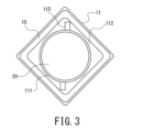
- FIG. 3 is an external perspective view showing another concave container of an electrochemical device.
- FIG. 4 is a plan view showing the electrochemical element of FIG. 1 (excluding the lid material and the conductive plate).
- FIG. 5 is a sectional view showing a conductive plate according to Modification Example 1.
- 6 is a perspective view showing the conductive plate of FIG. 5.
- FIG. FIG. 7 is a plan view showing a conductive plate according to Modification Example 2.
- FIG. 8 is a plan view showing a conductive plate according to modification 3.
- FIG. 9 is a sectional view showing a conductive plate according to Modification Example 4.
- FIG. 10 is a plan view showing a conductive plate according to modification 5.
- FIG. 11 is a plan view showing a conductive plate according to modification 6.
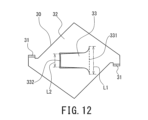
- FIG. 12 is a plan view showing a conductive plate according to Modification Example 7.
- FIG. 13 is a plan view showing a conductive plate according to Modification Example 8.
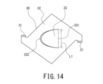
- FIG. 14 is a plan view showing a conductive plate according to modification example 9.
- FIG. 15 is a sectional view showing a conductive plate according to Modification Example 10.
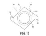
- FIG. 16 is a plan view showing the conductive plate of FIG. 15.
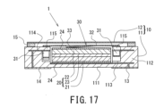
- FIG. 17 is a sectional view showing an electrochemical device according to the second embodiment.
- FIG. 18 is a cross-sectional view showing an electrochemical device according to the third embodiment.
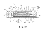
- FIG. 19 is a cross-sectional view showing an electrochemical device according to the fourth embodiment.
- An electrochemical device includes a case including a concave container having a bottom and a side wall, a lid material covering an opening of the concave container, and a first container sealed in the case and disposed on the bottom side.
- a power generation element having an electrode layer, a second electrode layer disposed on the lid material side, and an isolation layer disposed between the first electrode layer and the second electrode layer, and a power generation element disposed between the power generation element and the lid material. It is equipped with a conductive plate.
- the first electrode layer is electrically connected to a first conduction path leading from the inside of the case to the outside.
- the second electrode layer is electrically connected to a second conduction path leading from the inside of the case to the outside via a conductive plate.
- the conductive plate includes a flat part facing the power generating element, and a spring part rising from the flat part and pressing the power generating element toward the bottom of the concave container, so that the conductive plate is radially outward of the power generating element in the concave container in a plan view. It is locked to the side wall. A gap is formed between the conductive plate and the lid material.
- the conductive plate is latched and fixed to the side wall of the concave container at a position radially outward from the power generating element in plan view, and the spring portion of the conductive plate moves the power generating element toward the bottom side of the concave container.
- the conductive plate can more stably connect the power generation element to the first conduction path and the second conduction path without causing displacement of the conductive plate due to vibration or the like. This allows the electrochemical element to maintain good electrical connection.
- the lid material does not come into contact with the conductive plate, the lid material is not affected by pressure from the conductive plate during sealing, and the sealing performance of the case can be improved.
- the spring portion may include a spring piece that is supported in a cantilever manner on the plane portion and presses the power generation element toward the bottom of the concave container.
- the conductive plate may have a plurality of spring parts that rise from the plane part and press the power generation element toward the bottom of the concave container. This increases the number of electrically conductive locations between the conductive plate and the power generation element, thereby reducing electrical resistance and making the electrical connection more reliable. Further, the pressing points of the power generation element can be dispersed, and the overall pressing force can be increased.
- each of the plurality of spring parts may have a spring piece that is supported in a cantilever manner on the plane part and that presses the power generation element toward the bottom of the concave container. Accordingly, since it is sufficient to form the spring pieces at a plurality of locations on the flat surface of the conductive plate, it is possible to easily manufacture the conductive plate, that is, manufacture the electrochemical device.
- each of the plurality of spring pieces may be arranged line-symmetrically or point-symmetrically in a plan view. That is, each of the plurality of spring pieces may be arranged so as to have at least one of line symmetry and point symmetry in plan view. As a result, the contact points between the tip of the spring piece and the power generation element are arranged symmetrically, so that the pressing force of the spring piece on the power generation element can be evenly distributed.
- the spring pieces in the plurality of spring parts may be arranged radially in a plan view.
- the contact points between the tip of the spring piece and the power generation element are arranged symmetrically, so that the pressing force of the spring piece on the power generation element can be evenly distributed.
- the spring piece may be formed so that the width of the spring piece supported in a cantilever manner on the plane part is wider than the width of the tip part. Thereby, stress concentration on the cantilevered portion can be alleviated, and damage to the spring piece can be suppressed.
- the tip of the spring piece by making the width of the tip of the spring piece that is electrically connected to the second electrode layer narrower than the width of the tip that is cantilevered on the flat part, the tip of the spring piece can be easily bent, and the thickness of the power generation element can be reduced. Variations and variations in the height of the side wall of the concave container can be easily absorbed.
- the spring piece may be formed so that the width of the tip portion is wider than the width of the spring piece that is supported in a cantilever manner by the flat portion. This expands the electrical connection between the spring piece and the power generation element, thereby reducing electrical resistance.
- the spring piece may be a disc spring. Thereby, even if the thickness of the spring piece is reduced, the pressing force of the spring piece against the power generation element can be improved.
- the tip of the spring piece may be bent in the opposite direction to the power generation element. This can prevent the sharp tip of the spring piece from contacting and damaging the power generation element.
- the power generation element may further include a porous metal layer on the surface of the second electrode layer.
- the porous metal layer pressed by the conductive plate is compressed by a certain amount, and it is possible to sufficiently absorb variations in the thickness of the power generation element or the height of the case, and as a result, variations in the value of internal resistance can be reduced. Can be suppressed.
- the porous metal layer is integrated with the second electrode layer in advance, it is possible to reduce the electrical resistance at the electrical connection point between the spring portion and the power generation element.
- An electrochemical device includes a case including a concave container having a bottom portion and a side wall portion, and a lid member that covers an opening of the concave container; an exterior material including a first electrode terminal and a second electrode terminal disposed on the lid material side; a first electrode layer, a second electrode layer, a first electrode layer, and a second electrode layer;
- the present invention includes a flat element having a power generation element including an isolation layer disposed therebetween, and a conductive plate disposed between the flat element and the lid.
- the first electrode terminal is electrically connected to a first conduction path leading from the inside of the case to the outside.
- the second electrode terminal is electrically connected to a second conduction path leading from the inside of the case to the outside via the conductive plate.
- the conductive plate includes a flat part facing the flat element, and a spring part that rises from the flat part and presses the flat element toward the bottom of the concave container. It is locked to the side wall of the concave container. A gap is formed between the conductive plate and the lid. As a result, the electrochemical element can maintain good electrical connection without causing any displacement of the conductive plate due to vibration or the like. Further, since the lid material does not come into contact with the conductive plate, the lid material is not affected by pressure from the conductive plate during sealing, and the sealing performance of the case can be improved.
- the spring portion may include a spring piece that is supported in a cantilever manner on the plane portion and presses the flat element toward the bottom of the concave container.
- the electrochemical device 1 includes a case 10, a power generation element 20 and a conductive plate 30 housed in the case 10, and an external terminal 13 and an external terminal 14 arranged on the outer surface of the case 10. It is composed of.
- the case 10 has a concave container 11 and a lid member 12.
- the concave container 11 is made of ceramics.
- the concave container 11 includes a square bottom 111 and a square cylindrical side wall 112 that is formed continuously from the outer periphery of the bottom 111 and has a cylindrical space for accommodating the power generation element 20 therein. There is.
- the side wall portion 112 is provided so as to extend substantially perpendicularly to the bottom portion 111 when viewed in longitudinal section.
- a conductor portion 113 is formed inside the bottom portion 111 .
- the conductor portion 113 extends between the power generation element 20 and the bottom portion 111 so as to be conductively connected to the power generation element 20, and forms a conduction path corresponding to the electrode layer 21.
- a conductor portion 114 is formed inside the side wall portion 112 . As shown in FIG. 1, a part of the conductor part 114 is formed on the inner peripheral surface of the side wall part 112 to be exposed to the lower surface and side surface of the support part 115, which will be described later, and has a conductive path corresponding to the electrode layer 22. is formed. A method for manufacturing the concave container 11 will be described later. Note that the material of the concave container 11 is not particularly limited, and various materials such as resin, glass (borosilicate glass, glass ceramics, etc.), metal, and ceramic can be used. It may also be a composite material in which ceramic or glass powder is dispersed in a resin.
- the concave container 11 is made of a metal material, in order to ensure insulation between the concave container 11 and the power generation element 20, or between the concave container 11 and a flat element 50 (see FIG. 19) to be described later, It is preferable that the inner surface of the bottom portion 111 and the inner peripheral surface of the side wall portion 112 of the concave container 11 be coated with an insulating material such as a resin material or glass. Furthermore, the concave container 11 is not limited to a rectangular shape in plan view, but may have a circular shape, an elliptical shape, a polygonal shape, or the like.
- the internal space for accommodating the power generation element 20 is not limited to a cylindrical shape, but may be formed in a polygonal cylinder shape such as a square cylinder shape depending on the shape of the power generation element 20.
- the conductor portion 114 may be formed on the inner surface of the side wall portion 112 instead of inside the side wall portion 112, and may further penetrate the inside of the bottom portion 111 to be electrically connected to the external terminal 14.
- an insulating layer may be formed between the outer circumferential surface of the power generating element 20 and the conductor section 114, for example, on the inner surface of the conductor section 114, so that the outer circumferential surface of the power generating element 20 and the conductor section 114 do not come into contact with each other. preferable.
- the side wall portion 112 has a plurality of support portions 115 that support the conductive plate 30 described below.
- the support portion 115 is a projecting portion that is formed at the upper end of the inner circumferential surface of the side wall portion 112 and protrudes along the circumferential direction of the inner circumferential surface. More specifically, the support portion 115 is a top wall of a plurality of depressions formed radially outward on the inner peripheral surface of the side wall portion 112, as shown in FIG. Thereby, the support portion 115 is formed so as to protrude in the circumferential direction of the inner circumferential surface.
- each support portion 115 that is, the lower surface of each ceiling wall, locks and supports a supported portion 31 of a conductive plate 30, which will be described later, radially outward of the power generation element 20 in plan view. be able to.
- four supporting parts 115 are provided in this embodiment, the number is not limited. For example, when the number of supported parts 31 of the conductive plate 30 is two, the number of supporting parts 115 corresponding to the supported parts 31 is Two supporting parts 115 may be provided at the positions.
- the lid material 12 is a rectangular thin metal plate that covers the opening of the concave container 11. As shown in FIGS. 1 and 3, the lid member 12 is joined to the concave container 11 by a square frame-shaped seal ring 15 disposed between the lower surface of its outer peripheral end and the upper end of the concave container 11 (seam welding). ) has been done. Thereby, the internal space of the case 10 is completely sealed.
- the interior space of the case 10 is preferably a vacuum atmosphere or an inert gas atmosphere such as nitrogen, considering the influence on the power generation element 20. Note that the lid material 12 is not limited to a thin metal plate as long as it can cover the opening of the concave container 11.
- the lid material 12 is not limited to a rectangular shape, but can be variously changed to a circular shape, an elliptical shape, a polygonal shape, etc. depending on the shape of the concave container 11 in a plan view. Moreover, the lid material 12 may have a shape other than a flat plate. Note that the lid 12 may be bonded to the concave container 11 with an adhesive, and the method of joining the lid 12 and the concave container 11 is not particularly limited as long as the internal space of the case 10 can be sealed.
- the external terminal 13 is arranged on the outer surface of the bottom 111 of the concave container 11.
- the external terminal 13 is electrically connected to an electrode layer 21, which will be described later, via a conductor portion 113.
- the electrode layer 21 functions as a positive electrode layer as described later. Therefore, the conductor portion 113 becomes a conduction path that connects the external terminal 13 and the positive electrode layer, and the external terminal 13 functions as a positive electrode terminal.
- the external terminal 14 is arranged on the outer surface of the bottom 111 of the concave container 11 away from the external terminal 13.
- the external terminal 14 is electrically connected to a supported portion 31 of a conductive plate 30, which will be described later, via a conductor portion 114.
- the conductive plate 30 is electrically connected to the electrode layer 22 functioning as a negative electrode layer. Therefore, the conductor portion 114 becomes a conduction path that connects the external terminal 14 and the negative electrode layer, and the conductive plate 30 functions as a connection terminal that connects this conduction path and the electrode layer 22. Functions as a terminal.
- the arrangement of the external terminals 13 and 14 is not limited to the above, and may be arranged on the outer surface of the side wall portion 112 of the concave container 11, with the lid member 12 functioning as the conductor portion 114, and the external terminals 14 It is also possible to form it on the outer surface of the lid material 12. However, by arranging these terminals on the outer surface of the bottom 111 of the concave container 11 at a constant interval, mounting on the surface of the circuit board becomes easier.
- a method for manufacturing the concave container 11 will be explained.
- a printed pattern that will become the conductor portions 113 and 114 is formed by printing and coating a ceramic green sheet with a metal paste.
- a plurality of green sheets having these printed patterns formed thereon are laminated and fired.
- the above-mentioned support portion 115 is formed by stacking a plurality of green sheets having different shapes.
- this manufacturing method is not limited as long as the support portion 115 can be formed on the inner circumferential surface of the side wall portion 112.
- the external terminals 13 and 14 can also be formed by printing patterns of this metal paste.
- the power generation element 20 includes a laminate in which an electrode layer (positive electrode layer) 21, an electrode layer (negative electrode layer) 22, and a solid electrolyte layer 23 are stacked. Solid electrolyte layer 23 is arranged between electrode layer 21 and electrode layer 22 as a separation layer. That is, in this embodiment, the isolation layer is the solid electrolyte layer 23.
- the power generation element 20 is formed into a cylindrical shape.
- the power generation element 20 includes an electrode layer 21, a solid electrolyte layer 23, and an electrode layer 22 stacked in this order from the bottom 111 side (lower side in the drawing) of the concave container 11.
- the power generation element 20 is arranged such that the electrode layer 21, which is one end thereof, is on the bottom 111 side of the concave container 11, and the electrode layer 22, which is the other end, is on the lid material 12 side. They are arranged in such a manner that they become symmetrical, and are accommodated in the internal space of the case 10.
- the power generation element 20 is not limited to a cylindrical shape, and can be modified into various shapes such as a rectangular parallelepiped shape and a polygonal column shape.
- the power generation element 20 may have a plurality of laminates. The plurality of laminates may be stacked so as to be connected in series.
- the electrode layer 21 is made of a positive electrode mixture containing lithium cobalt oxide as a positive electrode active material, a sulfide-based solid electrolyte, and graphene as a conductive agent in a mass ratio of 65:30:5 in a cylindrical shape. This is a molded positive electrode pellet.
- the positive electrode active material of the electrode layer 21 is not particularly limited as long as it can function as the positive electrode layer of the power generation element 20, and examples thereof include lithium nickelate, lithium manganate, lithium nickel cobalt manganese composite oxide, It may be an olivine-type complex oxide or the like, or it may be an appropriate mixture of these. There are no particular limitations on other constituent materials or proportions. Further, the size and shape of the electrode layer 21 are not limited to a cylindrical shape, and can be changed in various ways depending on the size and shape of the electrochemical element 1.
- the electrode layer 22 contains LTO (Li 4 Ti 5 O 12 , lithium titanate), a sulfide-based solid electrolyte, and graphene in a weight ratio of 50:40 as a negative electrode active material used in a lithium ion secondary battery.
- This is a negative electrode pellet formed into a cylindrical shape from a negative electrode mixture containing 10 parts.
- the negative electrode active material of the electrode layer 22 is not particularly limited as long as it can function as the negative electrode layer of the power generation element 20, and examples thereof include metallic lithium, lithium alloy, and carbon such as graphite and low crystal carbon. It may be a material, an oxide such as SiO, or a mixture of these as appropriate. There are no particular limitations on other constituent materials or proportions. Further, the size and shape of the electrode layer 22 are not limited to a cylindrical shape, and can be changed in various ways depending on the size and shape of the electrochemical element 1.
- the solid electrolyte layer (separation layer) 23 includes a sulfide-based solid electrolyte.
- the solid electrolyte layer 23 is formed into a cylindrical shape.
- the solid electrolyte contained in the electrode layer 21, the electrode layer 22, and the solid electrolyte layer 23 is not particularly limited, but from the viewpoint of ionic conductivity, a sulfide-based solid electrolyte, particularly an argyrodite-type sulfide-based solid electrolyte is preferable. used.
- the surface of the positive electrode active material is preferably coated with a lithium ion conductive material such as niobium oxide in order to prevent reaction with the positive electrode active material.
- the solid electrolyte included in the solid electrolyte layer 23, the electrode layer 21, and the electrode layer 22 may be a hydride solid electrolyte, an oxide solid electrolyte, or the like.
- the size and shape of the solid electrolyte layer 23 are not limited to a cylindrical shape, and can be changed in various ways depending on the size and shape of the electrochemical element 1.
- the conductive plate 30 is a metal plate that is square in plan view and is installed in the opening of the concave container 11 of the case 10.
- the conductive plate 30 has a plurality of supported portions 31 that correspond to the positions of the respective supporting portions 115 described above, radially outward of the power generation element 20 in a plan view.
- the supported part 31 is the above-mentioned support part 115, that is, a hook-shaped locking piece that is locked to the lower surface of the ceiling wall. More specifically, the supported portion 31 extends from the edge of the conductive plate 30 toward the above-mentioned support portion 115 (downward in FIG. 1).
- the supported portion 31 has a supporting portion 115, that is, a tip that is folded back toward the lower surface of the ceiling wall.
- the tip of the supported portion 31 is in contact with the conductor portion 114 exposed on the lower surface and side surface of the above-mentioned ceiling wall.
- the conductive plate 30 functions as a current collector, and also functions as a connection terminal that electrically connects the electrode layer 22 and the conduction path leading to the external terminal 14.
- the conductive plate 30 is supported by a support portion 115 formed on the inner peripheral surface of the concave container 11 and covers a part of the opening of the concave container 11 .
- the area of the conductive plate 30 in plan view is smaller than the opening area of the concave container 11.
- the conductive plate 30 is pressed into the recess formed in the inner circumferential surface of the side wall portion 112. If the conductive plate 30 can be fixed, it is assumed that the conductive plate 30 is locked to the side wall portion 112 of the concave container 11.
- the conductive plate 30 extends from the flat part 32 of the conductive plate 30 to the electrode layer 22 of the power generating element 20 so as to contact the upper surface of the electrode layer 22, which is the other end of the power generating element 20. It has a spring portion 33 that stands up toward the front.
- the shape of the spring portion 33 is not particularly limited as long as it can press the power generation element 20 toward the bottom 111 of the concave container 11 .
- the spring portion 33 is a spring piece that is inclined from the plane portion 32 toward the electrode layer 22 of the power generation element 20 (hereinafter, the spring portion 33 may be referred to as the spring piece 33). As shown in FIG.
- the spring piece 33 is formed by cutting out a part of the flat part 32 in a U-shape, and is supported by the flat part 32 in a cantilever manner. That is, in this embodiment, the spring piece 33 is a plate spring. In this manner, since the spring pieces 33 may be formed on a portion of the flat portion 32, the conductive plate, that is, the electrochemical device can be easily manufactured. Further, by notching the flat portion 32 to form the spring pieces 33, the manufacturing of the conductive plate, that is, the manufacturing of the electrochemical device can be performed even more easily.
- the spring piece 33 has a boundary 331 with the plane portion 32 and a tip portion 332 that is brought into contact with the electrode layer 22 of the power generating element 20 to be electrically connected to the electrode layer 22 .
- the spring piece 33 is bent at the boundary 331 and is inclined toward the power generation element 20 from the boundary 331 toward the tip 332 .
- the height from the bottom of the flat part 32 to the tip 332 before the electrochemical element 1 is assembled is the height from the bottom of the flat part 32 to the power generation element 20 after the electrochemical element 1 is assembled. greater than the height of.
- the power generation element 20 can be pressed by the tip 332 of the spring piece 33, and a good electrical connection between the conductive plate 30 and the power generation element 20 can be maintained.
- the spring portion 33 by configuring the spring portion 33 with a spring piece, the thickness of the conductive plate 30 excluding the supported portion 31 can be reduced.
- the thickness of the conductive plate 30 excluding the supported portion 31 can be the sum of the thickness of the plate material constituting the plane portion 32 and the height of the spring piece 33. Specifically, by combining the thickness of the plate material: 0.2 mm and the height of the spring piece 33: 0.5 mm, the thickness of the conductive plate 30 excluding the supported portion 31 can be set to 0.7 mm. Further, the width of the spring piece 33 can be 1.5 mm, and the length can be 3 mm. Note that when a plurality of spring pieces 33 are provided, the shape including the width, length, etc. of the spring pieces 33 may be individually different for reasons such as preventing resonance.
- the thickness of the conductive plate 30 excluding the supported portion 31 is preferably 1.2 mm or less, more preferably 1 mm or less, and particularly preferably 0.8 mm or less.
- the thickness of the conductive plate 30 excluding the supported part 31 is preferably 0.3 mm or more, more preferably 0.4 mm or more, It is particularly preferable to set it to 0.5 mm or more.
- the edge of the conductive plate 30, that is, the position of the supported part 31, can be freely set in the height direction (thickness direction of the conductive plate 30), a gap is created between the lid member 12 and the conductive plate 30. Even when formed, the distance between the lid member 12 and the tip portion 332 of the spring piece 33 does not become large. As a result, it is possible to suppress the gap between the lid material 12 and the power generation element 20 from increasing, so that the capacity of the electrochemical element 1 can be increased.
- the overall thickness of the conductive plate 30 including the supported portion 31 can be adjusted as appropriate depending on the height of the side wall portion 112 of the concave container 11 from the bottom portion 111.
- the supported part 31 only needs to have a height necessary for locking to the support part 115.
- the entire thickness of the conductive plate 30 including the supported portion 31 can be, for example, 3 mm or less, preferably 2.7 mm or less, and more preferably 2.5 mm or less.
- the thickness direction is the vertical direction in FIG. 1 (height direction of the electrochemical element 1), and can also be said to be a direction perpendicular to the bottom surface of the flat portion 32 in the drawing.
- the spring piece 33 may be formed by notching the flat part 32 as described above, and in the modification described later, the spring piece 33 can be attached by separately welding the spring piece 33 to the bottom surface of the flat flat part 32. You can.
- a base for attaching the spring piece 33 may be provided in advance separately from the plane part 32, and the spring piece 33 may be attached to the base to make the entire spring part. That is, the spring piece 33 may stand up directly from the plane part 32, or may stand up from the plane part 32 with another element such as a base interposed therebetween. Moreover, both ends of the spring piece 33 may be supported by the flat part 32 so that the spring piece 33 has a convex shape toward the power generation element 20.
- Examples of metals constituting the conductive plate 30 include nickel, iron, copper, chromium, cobalt, titanium, aluminum, and alloys thereof, and in order to facilitate the function as a leaf spring, SUS301-CSP and SUS304-CSP are used. , SUS316-CSP, SUS420J2-CSP, SUS631-CSP, and SUS632J1-CSP are preferably used for springs.
- the thickness of the plate material of the conductive plate 30 is preferably 0.05 mm or more, more preferably 0.07 mm or more, and 0.1 mm or more in order to maintain the pressing force on the power generation element 20 at a certain level or more. It is particularly preferable to set it as above.
- the thickness of the conductive plate 30 is preferably 0.5 mm or less, more preferably 0.4 mm or less, and particularly preferably 0.3 mm or less.
- the conductive plate 30 is placed on the top surface of the power generating element 20 after the power generating element 20 is accommodated inside the concave container 11.
- the tip of the supported part 31 is connected to the top surface of the power generation element 20 and the support part 115, in the axial direction of the power generation element 20 (vertical direction in FIG. 1) In other words, it is positioned between it and the lower surface of the ceiling wall.
- the supported portion 31 is supported by the supporting portion 115. More specifically, the tip of the supported portion 31 is locked to the support portion 115, that is, the lower surface of the ceiling wall.
- the spring piece 33 of the conductive plate 30 Since the supported portion 31 is pushed downward, the spring piece 33 of the conductive plate 30 is pushed in the opposite direction to the electrode layer 22 while being in contact with the power generation element 20 .
- the spring piece 33 presses the power generation element 20 toward the bottom 111 of the concave container 11 by its elastic force. Thereby, the conductive plate 30 can come into more stable contact with the power generation element 20, and can maintain a good electrical connection without being misaligned due to vibration or the like.
- the spring piece 33 is not particularly limited as long as it can press the power generation element 20 toward the bottom 111 of the concave container 11 with its elastic force.
- the concave container 11 has two support parts 115, the number of support parts 115 may be two or more.
- the supported parts 31 may be formed according to the number of supporting parts 115. Note that as a method for fixing the edge of the conductive plate 30 (supported part 31 ) to the inner circumferential surface of the side wall 112 of the concave container 11 , the edge of the conductive plate 30 is fixed to the inner circumferential surface of the side wall 112 of the concave container 11 . A method of gluing the ends is also exemplified.
- a gap is formed between the conductive plate 30 and the lid material 12. That is, the conductive plate 30 and the lid member 12 do not come into contact with each other. Thereby, even if the conductive plate 30 is pushed toward the lid 12 due to a change in the volume of the power generation element 20, deformation of the lid 12 can be suppressed. Further, the lid member 12 and the concave container 11 are welded together via the seal ring 15 as described above. By providing a gap between the conductive plate 30 and the lid member 12, the influence of welding heat on the power generation element 20 can be suppressed.
- the conductive plate 30 and the lid 12 do not come into contact with each other, when the lid 12 is bonded to the upper end surface of the side wall 112 of the concave container 11, it is not affected by the pressure from the conductive plate 30, and the case 10 is sealed. The stopping performance can be further improved.
- the conductive plate 30 of Modification 1 has two spring pieces 33.
- the two spring pieces 33 are arranged line-symmetrically in plan view. More specifically, the two spring pieces 33 are formed to be line symmetrical with respect to a predetermined virtual axis A on the plane portion 32. That is, the two spring pieces 33 are each inclined toward the virtual axis A from the plane portion 32 toward the electrode layer 22 of the power generation element 20, as shown by the inclination direction D in the figure. Therefore, the tips 332 of each of the two spring pieces 33 face each other across the virtual axis A. In other words, the two spring pieces 33 are formed so that they can be opened double-sidedly.
- a plurality of such two spring pieces 33 may be arranged in the direction along the virtual axis A.
- the two spring pieces 33 of Modification 1 are arranged in five rows in the direction along the virtual axis A, ten spring pieces 33 are formed.
- the plurality of spring pieces 33 so as to be symmetrical with respect to the predetermined virtual axis A in this way, the number of contact points between the tips 332 of the spring pieces 33 and the electrode layer 22 increases, thereby reducing the electrical resistance. can be reduced.
- the contact points between the tip 332 of the spring piece 33 and the electrode layer 22 are arranged symmetrically, the pressing force of the spring piece 33 on the electrode layer 22 is evenly distributed, and the overall pressing force is increased. be able to.
- the position of the virtual axis A can be arbitrarily determined as long as the plurality of spring pieces 33 can be formed and the power generation element 20 can be appropriately pressed.
- the conductive plate 30 of Modification 2 has two spring pieces 33.
- the two spring pieces 33 are arranged point-symmetrically in plan view. More specifically, the two spring pieces 33 are formed to be point symmetrical with respect to a virtual point C on the plane portion 32.
- the two spring pieces 33 have parallel inclination directions, and one of the spring pieces 33 has an inclination direction D opposite to that of the other spring piece 33.
- They are arranged as follows.
- the conductive plate 30 of Modification 2 may have two or more spring pieces 33. In this case, the plurality of spring pieces 33 are arranged in parallel so that the inclination directions D of the spring pieces 33 are parallel and the inclination directions of adjacent spring pieces 33 are alternate.
- Each of the plurality of spring pieces 33 has the same length in the inclination direction D.
- the number of contact points between the tip portion 332 of the spring piece 33 and the electrode layer 22 increases, and since the plurality of spring pieces 33 are arranged so that the inclination directions of the adjacent spring pieces 33 are alternate, the electrical Resistance can be reduced.
- the contact points between the tip 332 of the spring piece 33 and the electrode layer 22 are arranged symmetrically, the pressing force of the spring piece 33 on the electrode layer 22 is evenly distributed, and the overall pressing force is increased. be able to.
- the position of the virtual point C can be arbitrarily determined as long as the plurality of spring pieces 33 can be formed on the flat part 32 and the power generation element 20 can be pressed appropriately.
- the virtual point C is preferably determined at a position corresponding to the geometric center of the power generation element 20 in the plane portion 32.
- the conductive plate 30 of Modification 3 has four spring pieces 33.
- the four spring pieces 33 are formed by cutting out the flat part 32 in a cross shape.
- Each spring piece 33 is arranged on a virtual ray extending from the center point P.
- the inclination directions D of the four spring pieces 33 each face the center point P. That is, the lines connecting the inclination directions D of two opposing spring pieces 33 among the four spring pieces 33 intersect.
- the four spring pieces 33 are arranged on a virtual ray so that each spring piece 33 is equiangular with respect to the center point P.
- the angle ⁇ between the adjacent spring pieces 33 with respect to the center point P is 90°.
- each spring piece 33 can be a tangent to a circle centered on the center point P. Moreover, the length of each spring piece 33 in the direction of inclination D may be the same.
- the conductive plate 30 of Modification 3 is not limited to having four spring pieces 33, but may have two, three, or five or more spring pieces 33. Thereby, electrical resistance can be reduced, and further, the pressing force of the spring pieces 33 on the electrode layer 22 can be evenly distributed, and the overall pressing force can be increased.
- the conductive plate 30 of Modification 4 has a spring piece 33 whose tip 332 is bent in the opposite direction to the electrode layer 22.
- the tip portion 332 is formed in a convex shape toward the electrode layer 22. It is preferable that the tip portion 332 has a curved surface that is convex toward the electrode layer 22 .
- the tip portion 332 and the electrode layer 22 may be brought into plane contact by bending the tip portion 332 multiple times. For example, by bending the tip portion 322 twice, a contact surface with the electrode layer 22 can be formed at the tip portion 332. This can prevent the sharp portion of the tip portion 332 from contacting and damaging the electrode layer 22 .
- the tip end portion 332 of the spring piece 33 in other modified examples may be similarly bent.
- the conductive plate 30 of Modification 5 has a trapezoidal spring piece 33.
- the width L1 of the boundary 331 is wider than the width L2 of the tip 332.
- the width L1 of the boundary 331 may be rephrased as the width of the bending portion of the spring piece 33 bent with respect to the plane part 32, or the width of the spring piece 33 supported in a cantilever manner by the plane part 32.
- the width L1 of the tip portion 332 may be rephrased as the width of a portion of the power generation element 20 that contacts the electrode layer 22 (that is, a portion that is electrically connected to the electrode layer 22).
- the relatively long side may be the boundary 331, and the relatively short side may be the tip portion 332.
- the tip portion 332 having a relatively narrow width easily bends in the opposite direction to the electrode layer 22 , resulting in uneven thickness of the power generation element 20 or side wall of the concave container 11 . 112 can be easily absorbed.
- the boundary 331, which is a bending point, to be relatively long stress concentration on the boundary 331 can be alleviated, and damage to the conductive plate 30, such as the spring piece 33 coming off from the flat part 32, can be suppressed. .
- the conductive plate 30 of Modification 6 has an inverted trapezoidal spring piece 33.
- the width L2 of the tip portion 332 is wider than the width L1 of the boundary 331. This increases the number of contact points between the tip portion 332 of the spring piece 33 and the electrode layer 22, so that electrical resistance can be reduced and the pressing force of the spring piece 33 against the electrode layer 22 can be increased.
- the spring pieces 33 of the above-mentioned modified examples 5 and 6 when the tip portion 332 is bent like the spring piece 33 of the modified example 4, or when the tip portion 332 is bent due to contact with the electrode layer 22. In this case, the spring piece 33 contacts the electrode layer 22 closer to the boundary 331 than the tip. In this case, the width of the location where the spring piece 33 contacts the electrode layer 22, that is, the location where the spring piece 33 and the electrode layer 22 are electrically connected, is regarded as the width L2 of the tip portion 332.
- Modification 7 As shown in FIG. 12, the conductive plate 30 of Modification Example 7 is cut out in the vicinity of the boundary 331 in a curved shape in plan view. That is, the width L1 of the boundary 331 is wider than the width L2 of the tip 332. Thereby, the same effect as the spring piece 33 of the fifth modification can be achieved.
- the conductive plate 30 of Modification 8 has a triangular spring piece 33.
- the boundary 331 is a predetermined side of the triangular spring piece 33
- the tip 332 is the apex of the triangular spring piece 33. That is, the triangular spring piece 33 is tapered from the boundary 331 toward the tip 332.
- the tip portion 332 is a vertex, it actually has a predetermined width L2 (not shown) that makes contact with the electrode layer 22. Therefore, it can be said that in the spring piece 33 of Modified Example 8 as well, the width L1 of the boundary 331 is wider than the width L2 of the tip portion 332. Thereby, the same effect as the spring piece 33 of the fifth modification can be achieved.
- the conductive plate 30 of Modification 9 has a semi-elliptical spring piece 33.
- the semi-elliptical spring piece 33 is formed by cutting out the plane portion 32 in a U-shape.
- the semi-elliptical spring piece 33 tapers from a boundary 331 toward a tip 332.
- the tip portion 332 has a curved shape in plan view, it actually has a predetermined width L2 (not shown) that makes contact with the electrode layer 22. Therefore, in the spring piece 33 of Modification 9 as well, it can be said that the width L1 of the boundary 331 is wider than the width L2 of the tip portion 332. Thereby, the same effect as the spring piece 33 of the fifth modification can be achieved.
- the spring piece 33 of Modification 10 is a disc spring, and is a peripheral wall of a truncated cone whose diameter gradually decreases from the plane portion 32 toward the power generation element 20. That is, the diameter of the boundary 331 is larger than the diameter of the tip 332, and the length of the boundary 331 is longer than the length of the tip 332. Thereby, the same effect as the spring piece 33 of the fifth modification can be achieved.
- the spring pieces 33 of the first embodiment and the spring pieces 33 of Modifications 1 to 10 thereof may be provided on the conductive plate 30 in various combinations.
- the power generation element 20 has a porous metal layer 24.
- the porous metal layer 24 is disposed on the surface of the electrode layer 22 and contacts the tip 332 of the spring piece 33 to establish electrical continuity between the electrode layer 22 and the conductive plate 30 .
- the porous metal layer 24 is a porous metal base having a high porosity and pores penetrating from one surface to the other, like a foamed metal porous body, and cannot be compressed by pressing. , and functions as a current collector.
- the porous metal layer 24 covers the surface of the electrode layer 22.
- the porous metal layer 24 In order to lower the electrical resistance, the porous metal layer 24 must not only be in contact with the electrode layer 22, but also be partially embedded in the negative electrode mixture of the electrode layer 22 and integrated with the electrode layer 22. Preferably. Note that, as shown in FIG.
- a porous metal layer 24 may be disposed on the surface of the electrode layer 21 on the lower surface of the electrode layer 22, that is, on the bottom 111 side, and a part of the porous metal layer 24 is connected to the positive electrode of the electrode layer 21.
- the porous metal layer 24 may be provided so as to be embedded in the agent and integrated with the electrode layer 21.
- the porosity of the porous metal layer 24 is preferably 80% or more, more preferably 90% or more, in order to easily adjust variations in the thickness of the power generation element 20 due to compression. On the other hand, in order to ensure good conductivity, the porosity of the porous metal layer 24 is preferably 99% or less.
- the thickness of the porous metal layer 24 before assembling the electrochemical device 1 is preferably 0.1 mm or more, more preferably 0.3 mm or more, particularly preferably 0.5 mm or more; , is preferably 3 mm or less, more preferably 2 mm or less, and particularly preferably 1.5 mm or less.
- porous metal layer 24 By providing the porous metal layer 24 in this way, it is possible to sufficiently absorb variations in the thickness of the power generation element 20 or the height of the case 10, and as a result, variations in the value of internal resistance can be suppressed. I can do it. Alternatively, if the porous metal layer 24 is integrated with the second electrode layer in advance, the electrical resistance at the electrically conductive location between the spring portion 33 and the power generation element 20 can be reduced.
- the electrochemical device 1 of the second embodiment will be specifically described using FIG. 18.
- the explanation of the same configuration as the electrochemical device 1 of the first embodiment will be basically omitted, and only the configuration different from the electrochemical device 1 of the first embodiment will be explained. .
- the electrochemical device 1 of this embodiment has a conductive sheet 40 between the electrode layer 22 and the conductive plate 30.
- the conductive sheet 40 is a conductive carbon sheet made of expanded graphite, that is, a graphite sheet.
- a graphite sheet is manufactured as follows. First, acid-treated graphite particles, which are natural graphite treated with an acid, are heated. Then, the acid-treated graphite expands as the acid between its layers evaporates and foams. This expanded graphite (expanded graphite) is molded into a felt shape, and further rolled using a roll mill to form a sheet body.
- the conductive sheet 40 is manufactured by hollowing out the expanded graphite sheet into a circular shape.
- expanded graphite is formed by vaporizing acid and foaming acid-treated graphite. Therefore, the graphite sheet is formed into a porous shape. Therefore, the graphite sheet has not only the electrical conductivity of graphite itself, but also flexibility that conventional graphite products do not have.
- the method for producing the graphite sheet is not limited to this, and the graphite sheet may be made of a material other than expanded graphite, and the graphite sheet may be produced by any method.
- the apparent density of the graphite sheet is preferably 0.3 g/cm 3 or more, more preferably 0.7 g/cm 3 or more, and preferably 1.5 g/cm 3 or less, more preferably 1.3 g/cm 3 or less. It is better to This is because if the apparent density of the graphite sheet is too low, the graphite sheet will be easily damaged, and if the apparent density is too high, the flexibility will decrease. Note that the apparent density is not limited to the graphite sheet, and can also be applied to the conductive sheet 40 formed of other materials such as conductive tape.
- the thickness of the graphite sheet is preferably 0.05 mm or more, more preferably 0.07 mm or more, preferably 0.5 mm or less, and more preferably 0.2 mm or less. If the thickness of the graphite sheet is too small, the graphite sheet will be easily damaged, and if the thickness is too large, the graphite sheet will narrow the internal space of the case 10 that accommodates the power generation element 20, reducing the volume (thickness) of the power generation element 20 that can be accommodated. This is to do so.
- the conductive sheet 40 that is more flexible than the conductive plate, that is, easily deformable, the pressing force of the spring pieces 33 of the conductive plate 30 described above is more uniformly transmitted to the power generation element 20, and the power generation element 20 can be prevented from being damaged, and the electrical connection can be stabilized.
- the conductive sheet 40 may be placed between the electrode layer 21 and the bottom 111 of the concave container 11, as shown in FIG. Thereby, it is possible to further suppress damage to the power generation element 20 and stabilize the electrical connection.
- the electrochemical device 1 of this embodiment accommodates a flat element 50 in the internal space of the case 10.
- the flat element 50 includes an outer can (electrode terminal) 51, a sealing can (electrode terminal) 52, the above-described power generation element 20, and a gasket 53.
- the outer can 51 includes a circular flat part 511 and a cylindrical side wall part 512 that is continuously formed from the outer periphery of the flat part 511.
- the cylindrical side wall portion 512 is provided so as to extend substantially perpendicularly to the flat portion 511 when viewed in longitudinal section.
- the outer can 51 is made of a metal material such as stainless steel.
- the outer can 51 is arranged on the bottom 111 side of the concave container 11.
- the sealing can 52 includes a circular flat part 521 and a cylindrical peripheral wall part 522 that is continuously formed from the outer periphery of the flat part 521.
- the opening of the sealed can 52 faces the opening of the outer can 51.
- the sealing can 52 is made of a metal material such as stainless steel.
- the sealing can 52 is arranged on the lid material 12 side.
- the power generation element 20 is housed between the outer can 51 and the sealed can 52. Therefore, the outer can 51 functions as an electrode terminal connected to the conductor portion 113, and the sealed can 52 functions as the other electrode terminal connected to the conductive plate 30.
- the outer can 51 and the sealing can 52 are caulked with a gasket 53 between the cylindrical side wall 512 of the outer can 51 and the peripheral wall 522 of the sealing can 52 after the power generation element 20 is housed in the internal space. More specifically, the outer can 51 and the sealing can 52 are configured such that the openings of the outer can 51 and the sealing can 52 face each other, and the peripheral wall portion 522 of the sealing can 52 is placed inside the cylindrical side wall portion 512 of the outer can 51. After inserting, the gasket 53 is crimped between the cylindrical side wall portion 512 and the peripheral wall portion 522. As a result, the internal space formed by the outer can 51 and the sealing can 52 becomes airtight.
- the exterior can 51 and the sealing can 52 are exterior materials that enclose the power generation element 20 in their internal space.
- the exterior can 51 and the sealing can 52 are not limited to a circular shape in plan view, but can be changed into various shapes such as an elliptical shape or a polygonal shape.
- the gasket 53 is made of a resin material such as polyamide resin, polypropylene resin, or polyphenylene sulfide resin.
- the method for sealing the internal space formed by the outer can 51 and the sealing can 52 is not limited to caulking via the gasket 53, and may be performed by other methods.
- the cylindrical side wall portion 512 of the outer can 51 and the peripheral wall portion 522 of the sealing can 52 may be joined with a hot melt resin, an adhesive, or the like interposed therebetween, and sealed.
- the conductive plate 30 is placed on the upper surface of the flat element 50, and the supported part 31 is latched to and supported by the support part 115.
- the spring piece 33 of the conductive plate 30 is bent in the opposite direction to the flat element 50 while in contact with the flat part 521 of the sealed can 52.
- the spring piece 33 presses the flat element 50 in the direction of the bottom 111 of the concave container 11 by its elastic force.
- the conductive plate 30 is in more stable contact with the flat element 50 without being displaced due to vibrations or the like, and similarly to the electrochemical element 1 of the first embodiment described above, the conductive plate 30 is prevented from being displaced due to vibrations or the like. A good electrical connection can be maintained without any occurrence.
- the porous metal layer 24 or the conductive sheet 40 described above may be arranged between the flat element 50 and the conductive plate 30. Further, the porous metal layer 24 or the conductive sheet 40 may be disposed between the flat element 50 and the bottom 111 of the concave container 11.
- the flat element 50 is not limited to an all-solid battery having a solid electrolyte layer, but may also be a non-aqueous electrolyte battery such as a lithium ion secondary battery, another flat battery, or a capacitor such as a lithium ion capacitor. There may be.
- the electrode layer 21 functions as a positive electrode layer and the electrode layer 22 functions as a negative electrode layer, but the electrode layer 21 functions as a negative electrode layer and the electrode layer 22 functions as a negative electrode layer. You can make it work.
- the external terminal 13 functions as a negative terminal, and the external terminal 14 functions as a positive terminal.
- the flat element 50 is housed in the internal space of the case 10 such that the outer can 51 is placed on the bottom 111 side of the concave container 11, but the sealed can 52 is placed on the bottom side of the concave container 11. It may be housed so as to be placed on the 111 side. That is, the flat element 50 may be housed in the internal space of the case 10 with the flat element 50 shown in FIG. 6 turned upside down.
- the power generation element 20 is composed of a laminate in which the electrode layer 21, the electrode layer 22, and the solid electrolyte layer 23 are laminated.
- the electrochemical element can be used as a lithium ion secondary battery, a lithium ion capacitor, an electric double layer capacitor, etc. I can do it.
- the separator and electrolyte are those commonly used in lithium ion secondary batteries, lithium ion capacitors, electric double layer capacitors, and the like.
- the electrode layer 21 and the electrode layer 22 may be replaced with a mixture layer of a positive electrode and a negative electrode that are commonly used in various electrochemical devices 1.
- An electrochemical device (all-solid-state battery) shown in FIG. 9 was fabricated using a conductive plate made of SUS304-CSP with a thickness of 0.2 mm.
- the electrochemical device of this example was subjected to a vibration test as follows to evaluate its vibration resistance.
- the sine wave sweep was a logarithmic sweep that reciprocated in the range of 7 Hz to 200 Hz in 15 minutes while changing the frequency, and the sweep was repeated 12 times in each of the three directions. Note that between 7Hz and 18Hz, the sweep is performed so that the peak acceleration is maintained at 1G, and from 18Hz, the sweep is performed until the peak acceleration reaches 8G (approximately 50Hz) while maintaining the total amplitude at 0.8mm. Furthermore, a sweep was performed so that the peak acceleration was maintained at 1 G up to 200 Hz.
- the AC impedance at 1 kHz with an applied voltage of 10 mV was measured for the electrochemical element of the example subjected to the vibration test, and compared with the AC impedance value measured before the vibration test, but no change was observed, and a concave shape was observed. It was confirmed that the electrical connection was maintained well by the conductive plate attached to the side wall of the container.
Landscapes
- Chemical & Material Sciences (AREA)
- Chemical Kinetics & Catalysis (AREA)
- Electrochemistry (AREA)
- General Chemical & Material Sciences (AREA)
- Engineering & Computer Science (AREA)
- Power Engineering (AREA)
- Microelectronics & Electronic Packaging (AREA)
- Manufacturing & Machinery (AREA)
- Materials Engineering (AREA)
- Electric Double-Layer Capacitors Or The Like (AREA)
- Sealing Battery Cases Or Jackets (AREA)
Abstract
Description
本開示の実施形態に係る電気化学素子は、底部及び側壁部を有する凹状容器と凹状容器の開口を覆う蓋材とを有するケースと、ケース内に封止され、底部側に配置された第1電極層と蓋材側に配置された第2電極層と第1電極層及び第2電極層の間に配置された隔離層とを有する発電要素と、発電要素と蓋材との間に配置された導電板とを備えている。第1電極層は、ケースの内部から外部に通じる第1導通経路と電気的に接続されている。第2電極層は、導電板を介して前記ケースの内部から外部に通じる第2導通経路と電気的に接続されている。導電板は、発電要素に対向する平面部と、平面部から立ち上がり発電要素を凹状容器の底部方向へ押圧するバネ部とを含み、平面視で発電要素よりも径方向の外方において凹状容器の側壁部に係止されている。導電板と蓋材との間には隙間が形成されている。 (Configuration 1)
An electrochemical device according to an embodiment of the present disclosure includes a case including a concave container having a bottom and a side wall, a lid material covering an opening of the concave container, and a first container sealed in the case and disposed on the bottom side. A power generation element having an electrode layer, a second electrode layer disposed on the lid material side, and an isolation layer disposed between the first electrode layer and the second electrode layer, and a power generation element disposed between the power generation element and the lid material. It is equipped with a conductive plate. The first electrode layer is electrically connected to a first conduction path leading from the inside of the case to the outside. The second electrode layer is electrically connected to a second conduction path leading from the inside of the case to the outside via a conductive plate. The conductive plate includes a flat part facing the power generating element, and a spring part rising from the flat part and pressing the power generating element toward the bottom of the concave container, so that the conductive plate is radially outward of the power generating element in the concave container in a plan view. It is locked to the side wall. A gap is formed between the conductive plate and the lid material.
構成1の電気化学素子において、バネ部は、平面部に片持ち支持され、かつ、発電要素を凹状容器の底部方向へ押圧するバネ片を有してよい。これにより、導電板の平面部の一部にバネ片を形成すればよいため、導電板の製造、すなわち、電気化学素子の製造を容易に行うことができる。 (Configuration 2)
In the electrochemical element of
構成1の電気化学素子において、導電板は、平面部から立ち上がり発電要素を凹状容器の底部方向へ押圧する複数のバネ部を有してよい。これにより、導電板と発電要素との導通箇所が増すため、電気抵抗を低減させるとともに、電気的接続をより確実に行うことができる。また、発電要素の押圧箇所を分散させるとともに、全体の押圧力を高めることができる。 (Configuration 3)
In the electrochemical element of
構成3の電気化学素子において、複数のバネ部は各々、平面部に片持ち支持され、かつ、発電要素を凹状容器の底部方向へ押圧するバネ片を有してよい。これにより、導電板の平面部の複数個所にバネ片を形成すればよいため、導電板の製造、すなわち、電気化学素子の製造を容易に行うことができる。 (Configuration 4)
In the electrochemical element of configuration 3, each of the plurality of spring parts may have a spring piece that is supported in a cantilever manner on the plane part and that presses the power generation element toward the bottom of the concave container. Accordingly, since it is sufficient to form the spring pieces at a plurality of locations on the flat surface of the conductive plate, it is possible to easily manufacture the conductive plate, that is, manufacture the electrochemical device.
構成4の電気化学素子において、複数のバネ片は各々、平面視で線対称又は点対称となるように配置されてよい。すなわち、複数のバネ片は各々、平面視で線対称及び点対称の少なくともいずれか一方となるように配置されてよい。これにより、バネ片の先端部と発電要素との接触箇所が対照的に配置されるため、バネ片の発電要素への押圧力を均等に分散させることができる。 (Configuration 5)
In the electrochemical element of configuration 4, each of the plurality of spring pieces may be arranged line-symmetrically or point-symmetrically in a plan view. That is, each of the plurality of spring pieces may be arranged so as to have at least one of line symmetry and point symmetry in plan view. As a result, the contact points between the tip of the spring piece and the power generation element are arranged symmetrically, so that the pressing force of the spring piece on the power generation element can be evenly distributed.
構成4の電気化学素子において、複数のバネ部におけるバネ片は各々、平面視で放射状に配置されてよい。これにより、バネ片の先端部と発電要素との接触箇所が対照的に配置されるため、バネ片の発電要素への押圧力を均等に分散させることができる。 (Configuration 6)
In the electrochemical element of Configuration 4, the spring pieces in the plurality of spring parts may be arranged radially in a plan view. As a result, the contact points between the tip of the spring piece and the power generation element are arranged symmetrically, so that the pressing force of the spring piece on the power generation element can be evenly distributed.
構成2の電気化学素子において、バネ片は、平面部に片持ち支持されている幅が先端部の幅よりも広くなるように形成されてよい。これにより、片持ち支持されている箇所への応力集中を緩和し、バネ片の破損を抑制することができる。また、バネ片において第2電極層と導通させる先端部の幅を、平面部に片持ち支持されている幅よりも狭くすることで、バネ片の先端部が撓み易くなり、発電要素の厚みのばらつきや凹状容器の側壁部の高さのばらつき等を容易に吸収することができる。 (Configuration 7)
In the electrochemical element of configuration 2, the spring piece may be formed so that the width of the spring piece supported in a cantilever manner on the plane part is wider than the width of the tip part. Thereby, stress concentration on the cantilevered portion can be alleviated, and damage to the spring piece can be suppressed. In addition, by making the width of the tip of the spring piece that is electrically connected to the second electrode layer narrower than the width of the tip that is cantilevered on the flat part, the tip of the spring piece can be easily bent, and the thickness of the power generation element can be reduced. Variations and variations in the height of the side wall of the concave container can be easily absorbed.
構成2の電気化学素子において、バネ片は、先端部の幅が平面部に片持ち支持されている幅よりも広くなるように形成されてよい。これにより、バネ片と発電要素との導通箇所が広がるため、電気抵抗を低減させることができる。 (Configuration 8)
In the electrochemical element of configuration 2, the spring piece may be formed so that the width of the tip portion is wider than the width of the spring piece that is supported in a cantilever manner by the flat portion. This expands the electrical connection between the spring piece and the power generation element, thereby reducing electrical resistance.
構成2の電気化学素子において、バネ片は、皿バネであってよい。これにより、バネ片の厚みを薄くしても、バネ片の発電要素への押圧力を向上させることができる。 (Configuration 9)
In the electrochemical element of configuration 2, the spring piece may be a disc spring. Thereby, even if the thickness of the spring piece is reduced, the pressing force of the spring piece against the power generation element can be improved.
構成2、4~9のいずれかの電気化学素子において、バネ片の先端部は、発電要素とは反対方向に折り曲げられてよい。これにより、バネ片の先端部の鋭利な箇所が発電要素に接触して傷つけるのを防ぐことができる。 (Configuration 10)
In the electrochemical device of any of configurations 2, 4 to 9, the tip of the spring piece may be bent in the opposite direction to the power generation element. This can prevent the sharp tip of the spring piece from contacting and damaging the power generation element.
構成1~10のいずれかの電気化学素子において、発電要素は、第2電極層の表面にさらに多孔質金属層を有してよい。これにより、導電板から押圧された多孔質金属層が一定量圧縮され、発電要素の厚み又はケースの高さ等のばらつきを十分に吸収することができ、その結果、内部抵抗の値のばらつきを抑制することができる。或いは、多孔質金属層が予め第2電極層と一体化されている場合には、バネ部と発電要素との導通箇所の電気抵抗を低減することができる。 (Configuration 11)
In the electrochemical device of any one of
本開示の他の実施形態に係る電気化学素子は、底部及び側壁部を有する凹状容器と凹状容器の開口を覆う蓋材とを有するケースと、ケース内に封止され、底部側に配置された第1電極端子及び蓋材側に配置された第2電極端子を含む外装材と、外装材の内部に封入され、第1電極層と第2電極層と第1電極層及び第2電極層の間に配置された隔離層とを含む発電要素とを有する扁平形素子と、扁平形素子と蓋材との間に配置された導電板とを備えている。第1電極端子は、ケースの内部から外部に通じる第1導通経路と電気的に接続されている。第2電極端子は、導電板を介してケースの内部から外部に通じる第2導通経路と電気的に接続されている。導電板は、扁平形素子に対向する平面部と、平面部から立ち上がり扁平形素子を凹状容器の底部方向へ押圧するバネ部とを含み、平面視で扁平形素子よりも径方向の外方において凹状容器の側壁部に係止されてている。導電板と前記蓋材との間には隙間が形成されている。これにより、電気化学素子は、振動等により導電板に位置ズレが生じることなく、良好な電気的接続を維持させることができる。また、蓋材が導電板と当接しないため、封止時に蓋材が導電板からの押圧等の影響を受けなくなり、ケースの封止性を向上させることができる。 (Configuration 12)
An electrochemical device according to another embodiment of the present disclosure includes a case including a concave container having a bottom portion and a side wall portion, and a lid member that covers an opening of the concave container; an exterior material including a first electrode terminal and a second electrode terminal disposed on the lid material side; a first electrode layer, a second electrode layer, a first electrode layer, and a second electrode layer; The present invention includes a flat element having a power generation element including an isolation layer disposed therebetween, and a conductive plate disposed between the flat element and the lid. The first electrode terminal is electrically connected to a first conduction path leading from the inside of the case to the outside. The second electrode terminal is electrically connected to a second conduction path leading from the inside of the case to the outside via the conductive plate. The conductive plate includes a flat part facing the flat element, and a spring part that rises from the flat part and presses the flat element toward the bottom of the concave container. It is locked to the side wall of the concave container. A gap is formed between the conductive plate and the lid. As a result, the electrochemical element can maintain good electrical connection without causing any displacement of the conductive plate due to vibration or the like. Further, since the lid material does not come into contact with the conductive plate, the lid material is not affected by pressure from the conductive plate during sealing, and the sealing performance of the case can be improved.
構成13の電気化学素子において、バネ部は、平面部に片持ち支持されかつ扁平形素子を凹状容器の底部方向へ押圧するバネ片を有してよい。これにより、導電板の平面部の一部にバネ片を形成すればよいため、導電板の製造、すなわち、電気化学素子の製造を容易に行うことができる。 (Configuration 13)
In the electrochemical device of
以下、本開示の第1実施形態について、電気化学素子が全固体電池である場合を例にして、図1~図16を用いて具体的に説明する。まず、図1に示すように、電気化学素子1は、ケース10と、ケース10に収容される発電要素20及び導電板30と、ケース10の外表面に配置される外部端子13及び外部端子14とから構成されている。 (First embodiment)
Hereinafter, the first embodiment of the present disclosure will be specifically described using FIGS. 1 to 16, taking as an example the case where the electrochemical element is an all-solid-state battery. First, as shown in FIG. 1, the
図5及び図6に示すように、変形例1の導電板30は、2つのバネ片33を有する。図6に示すように、2つのバネ片33は、平面視において線対称となるように配置されている。より具体的には、2つのバネ片33は、平面部32上の所定の仮想軸線Aに対して線対称となるように形成されている。すなわち、2つのバネ片33は各々、図中の傾斜方向Dで示すように、仮想軸線Aに向かって平面部32から発電要素20の電極層22へと傾斜している。したがって、2つのバネ片33の各々の先端部332は、仮想軸線Aを介して対向している。言い換えれば、2つのバネ片33は、観音開き可能に形成されている。このような2つのバネ片33は、仮想軸線Aに沿う方向に複数配列してもよい。例えば、変形例1の2つのバネ片33を仮想軸線Aに沿う方向に5列配置した場合、10個のバネ片33が形成される。このように所定の仮想軸線Aに対して線対称となるように複数のバネ片33を設けたことにより、バネ片33の先端部332と電極層22との接触箇所が増すため、電気抵抗を低減させることができる。また、バネ片33の先端部332と電極層22との接触箇所が対称的に配置されるため、バネ片33の電極層22への押圧力を均等に分散させるとともに、全体の押圧力を高めることができる。なお、仮想軸線Aの位置は、複数のバネ片33を形成することができ、かつ、発電要素20を適切に押圧できれば、任意に決めることができる。 (Modification 1)
As shown in FIGS. 5 and 6, the
図7に示すように、変形例2の導電板30は、2つのバネ片33を有する。2つのバネ片33は、平面視において点対称となるように配置されている。より具体的には、2つのバネ片33は、平面部32上の仮想点Cに対して点対称となるように形成されている。図中の傾斜方向Dで示すように、2つのバネ片33は、各々平行な傾斜方向を有し、かつ、一方のバネ片33は他方のバネ片33とは反対方向の傾斜方向Dを有するように配列されている。変形例2の導電板30は、2つ又は3つ以上の複数のバネ片33を有してもよい。この場合、バネ片33の傾斜方向Dが平行で、かつ、隣り合うバネ片33同士の傾斜方向が交互となるように複数のバネ片33が並設される。複数のバネ片33における各々の傾斜方向Dの長さは同じである。これにより、バネ片33の先端部332と電極層22との接触箇所が増し、また、隣り合うバネ片33同士の傾斜方向が交互となるように複数のバネ片33が配列されるため、電気抵抗を低減させることができる。また、バネ片33の先端部332と電極層22との接触箇所が対称的に配置されるため、バネ片33の電極層22への押圧力を均等に分散させるとともに、全体の押圧力を高めることができる。なお、仮想点Cの位置は、複数のバネ片33を平面部32に形成でき、かつ、発電要素20を適切に押圧できれば、任意に決めることができる。ただし、仮想点Cは、平面部32において発電要素20の幾何中心に相当する位置に決めることが好ましい。 (Modification 2)
As shown in FIG. 7, the
図8に示すように、変形例3の導電板30は、4つのバネ片33を有する。4つのバネ片33は、平面部32を十字状に切欠いて形成されている。各々のバネ片33は、中心点Pから延びる仮想放射線上に配置されている。4つのバネ片33の傾斜方向Dは各々、中心点Pを向いている。すなわち、4つのバネ片33のうち、対向する2つのバネ片33の傾斜方向Dを結ぶ線は交差している。4つのバネ片33は、各々のバネ片33は、中心点Pに対して等角となるように仮想放射線上に配置されている。本変形例3では、隣り合うバネ片33の中心点Pに対する角度θは、90℃である。各々のバネ片33の境界331は、中心点Pを中心とする円の接線とすることができる。また、各々のバネ片33の傾斜方向Dの長さは同じであってよい。変形例3の導電板30は4つのバネ片33を有するものに限られるものではなく、2つ、3つ、又は5つ以上の複数のバネ片33を有していてもよい。これにより、電気抵抗を低減させることができ、さらに、バネ片33の電極層22への押圧力を均等に分散させるとともに、全体の押圧力を高めるさせることができる。 (Modification 3)
As shown in FIG. 8, the
図9に示すように、変形例4の導電板30は、先端部332が電極層22とは反対方向に折り曲げられたバネ片33を有する。すなわち、先端部332は、電極層22に向かって凸状に形成されている。先端部332は、電極層22に向かって凸状の曲面を有することが好ましい。また、先端部332を複数折り曲げることにより、先端部332と電極層22とが面で接触するようにしてもよい。例えば、先端部322を2回折り曲げれば、先端部332に電極層22との接触面を形成することができる。これにより、電極層22に対して先端部332の鋭利な箇所が接触して傷つけるのを防ぐことができる。なお、他の変形例のバネ片33の先端部332を同様に折り曲げてもよい。 (Modification 4)
As shown in FIG. 9, the
図10に示すように、変形例5の導電板30は、台形状のバネ片33を有する。境界331の幅L1は、先端部332の幅L2よりも広い。境界331の幅L1は、平面部32に対して折り曲げられたバネ片33の折り曲げ箇所の幅、或いは、平面部32に片持ち支持されている幅と言い換えてもよい。先端部332の幅L1は、発電要素20の電極層22に接触する箇所(すなわち、電極層22と導通する箇所)の幅と言い換えてもよい。また、台形状のバネ片33の対辺のうち、比較的長い辺が境界331であり、比較的短い辺が先端部332であると言い換えてもよい。これにより、バネ片33が電極層22に接触したとき、比較的幅が狭い先端部332が電極層22とは反対方向に撓み易くなり、発電要素20の厚みのばらつき又は凹状容器11の側壁部112の高さのばらつき等を容易に吸収することができる。また、折り曲げ箇所である境界331を比較的長く形成したことにより、境界331への応力集中を緩和し、バネ片33が平面部32から離脱する等、導電板30の破損を抑制することができる。 (Modification 5)
As shown in FIG. 10, the
図11に示すように、変形例6の導電板30は、逆台形状のバネ片33を有する。先端部332の幅L2は、境界331の幅L1よりも広い。これにより、バネ片33の先端部332と電極層22との接触箇所が増すため、電気抵抗を低減させることができるとともに、バネ片33の電極層22への押圧力を高めることができる。なお、上述の変形例5及び変形例6のバネ片33において、変形例4のバネ片33のように先端部332を折り曲げた場合、或いは、電極層22との接触によって先端部332が撓んだ場合、バネ片33は、先端よりも境界331側において、電極層22と接触する。この場合、バネ片33が電極層22と接触する箇所、すなわち、バネ片33と電極層22とが導通する箇所の幅を、先端部332の幅L2とみなすものとする。 (Modification 6)
As shown in FIG. 11, the
図12に示すように、変形例7の導電板30は、境界331の近傍において平面視曲線状に切り欠かれている。すなわち、境界331の幅L1は、先端部332の幅L2よりも広い。これにより、変形例5のバネ片33と同様の効果を奏することができる。 (Modification 7)
As shown in FIG. 12, the
図13に示すように、変形例8の導電板30は、三角形状のバネ片33を有する。境界331は三角形状のバネ片33のうち所定の一辺であり、先端部332は三角形状のバネ片33の頂点である。すなわち、三角形状のバネ片33は、境界331から先端部332に向かって先細りになっている。ここで、先端部332は頂点であるものの、実際には電極層22と接触する所定の幅L2(図示せず。)を有する。したがって、変形例8のバネ片33においても、境界331の幅L1は、先端部332の幅L2よりも広いと言える。これにより、変形例5のバネ片33と同様の効果を奏することができる。 (Modification 8)
As shown in FIG. 13, the
図14に示すように、変形例9の導電板30は、半楕円形状のバネ片33を有する。半楕円形状のバネ片33は、平面部32をU字型に切欠いて形成されている。半楕円形状のバネ片33は、境界331から先端部332に向かって先細りになっている。ここで、先端部332は平面視曲線状であるものの、実際には電極層22と接触する所定の幅L2(図示せず。)を有する。したがって、変形例9のバネ片33においても、境界331の幅L1は、先端部332の幅L2よりも広いと言える。これにより、変形例5のバネ片33と同様の効果を奏することができる。 (Modification 9)
As shown in FIG. 14, the
図15及び図16に示すように、変形例10のバネ片33は、皿バネであり、平面部32から発電要素20に向かって徐々に径が小さくなる円錐台の周壁である。すなわち、境界331の直径は、先端部332の直径よりも大きく、境界331の長さは、先端部332の長さよりも長い。これにより、変形例5のバネ片33と同様の効果を奏することができる。 (Modification 10)
As shown in FIGS. 15 and 16, the
次に、第2実施形態の電気化学素子1について、図17を用いて具体的に説明する。本実施形態の電気化学素子1において、第1実施形態の電気化学素子1と同じ構成については基本的には説明を省略し、第1実施形態の電気化学素子1とは異なる構成についてのみ説明する。 (Second embodiment)
Next, the
次に、第2実施形態の電気化学素子1について、図18を用いて具体的に説明する。本実施形態の電気化学素子1において、第1実施形態の電気化学素子1と同じ構成については基本的には説明を省略し、第1実施形態の電気化学素子1とは異なる構成についてのみ説明する。 (Third embodiment)
Next, the
次に、第3実施形態の電気化学素子1について、図19を用いて具体的に説明する。本実施形態の電気化学素子1において、第1実施形態及び第2実施形態の電気化学素子1と同じ構成については基本的には説明を省略し、第1実施形態及び第2実施形態の電気化学素子1とは異なる構成についてのみ説明する。 (Fourth embodiment)
Next, the
厚さ0.2mmのSUS304-CSPで構成された導電板を用い、図9に示される電気化学素子(全固体電池)を作製した。この実施例の電気化学素子について、以下のようにして振動試験を行い、耐振動性を評価した。 [Evaluation of vibration resistance]
An electrochemical device (all-solid-state battery) shown in FIG. 9 was fabricated using a conductive plate made of SUS304-CSP with a thickness of 0.2 mm. The electrochemical device of this example was subjected to a vibration test as follows to evaluate its vibration resistance.
耐振試験とは別に、JIS-Z2331に記載された「ヘリウム漏れ試験方法」(ボンビング法)により、実施例の電気化学素子のケースの封止性を確認した。タンク内に電気化学素子を入れてヘリウムガスで2時間加圧した後、真空チャンバー内で電気化学素子の周囲を1分間真空排気してヘリウムガスのリーク量を求めたところ、10分後にはリーク量が1×10⁻¹⁰Pa・m3/s以下となり、優れた封止性を有することが確認された。 [Evaluation of sealability]
Apart from the vibration test, the sealability of the case of the electrochemical device of the example was confirmed by the "helium leak test method" (bombing method) described in JIS-Z2331. After placing the electrochemical device in a tank and pressurizing it with helium gas for 2 hours, we evacuated the area around the electrochemical device in a vacuum chamber for 1 minute to determine the amount of helium gas leaking, and found that it leaked after 10 minutes. The amount was 1×10 −10 Pa·m 3 /s or less, and it was confirmed that the sealant had excellent sealing properties.
1 electrochemical element, 10 case, 11 concave container, 12 lid, 13 external terminal, 14 external terminal, 15 seal ring, 111 bottom, 112 side wall, 113 conductor, 114 conductor, 115 support, 20 power generation element , 30 conductive plate, 31 supported part, 32 plane part, 33 spring piece, 331 boundary, 332 tip part, 40 conductive sheet, 50 flat element, 51 outer can, 511 plane part, 52 sealed can, 521 plane part, 53 Gasket, virtual axis A, virtual point C, center point P
Claims (13)
- 底部及び側壁部を有する凹状容器と前記凹状容器の開口を覆う蓋材とを有するケースと、
前記ケース内に封止され、前記底部側に配置された第1電極層と前記蓋材側に配置された第2電極層と前記第1電極層及び前記第2電極層の間に配置された隔離層とを有する発電要素と、
前記発電要素と前記蓋材との間に配置された導電板とを備え、
前記第1電極層は、前記ケースの内部から外部に通じる第1導通経路と電気的に接続されており、
前記第2電極層は、前記導電板を介して前記ケースの内部から外部に通じる第2導通経路と電気的に接続されており、
前記導電板は、前記発電要素に対向する平面部と、前記平面部から立ち上がり前記発電要素を前記凹状容器の底部方向へ押圧するバネ部とを含み、平面視で前記発電要素よりも径方向の外方において前記凹状容器の側壁部に係止されており、
前記導電板と前記蓋材との間には隙間が形成されている、電気化学素子。 a case having a concave container having a bottom portion and a side wall portion; and a lid material covering an opening of the concave container;
A first electrode layer that is sealed in the case and is placed on the bottom side, a second electrode layer that is placed on the lid side, and is placed between the first electrode layer and the second electrode layer. a power generation element having an isolation layer;
comprising a conductive plate disposed between the power generation element and the lid material,
The first electrode layer is electrically connected to a first conduction path leading from the inside of the case to the outside,
The second electrode layer is electrically connected to a second conduction path leading from the inside to the outside of the case via the conductive plate,
The conductive plate includes a flat part facing the power generating element, and a spring part rising from the flat part and pressing the power generating element toward the bottom of the concave container, and the conductive plate has a flat part facing the power generating element in a radial direction than the power generating element in a plan view. latched to the side wall of the concave container on the outside;
An electrochemical element, wherein a gap is formed between the conductive plate and the lid. - 請求項1に記載の電気化学素子であって、
前記バネ部は、前記平面部に片持ち支持され、かつ、前記発電要素を前記凹状容器の底部方向へ押圧するバネ片を有する、電気化学素子。 The electrochemical device according to claim 1,
An electrochemical element, wherein the spring part is supported in a cantilever manner by the flat part and has a spring piece that presses the power generation element toward the bottom of the concave container. - 請求項1に記載の電気化学素子であって、
前記導電板は、前記平面部から立ち上がり前記発電要素を前記凹状容器の底部方向へ押圧する複数のバネ部を有する、電気化学素子。 The electrochemical device according to claim 1,
The electrochemical element includes a plurality of spring parts in which the conductive plate rises from the flat part and presses the power generation element toward the bottom of the concave container. - 請求項3に記載の電気化学素子であって、
前記複数のバネ部は各々、前記平面部に片持ち支持され、かつ、前記発電要素を前記凹状容器の底部方向へ押圧するバネ片を有する、電気化学素子。 The electrochemical device according to claim 3,
Each of the plurality of spring parts has a spring piece that is cantilever-supported by the flat part and presses the power generation element toward the bottom of the concave container. - 請求項4に記載の電気化学素子であって、
前記複数のバネ部におけるバネ片は各々、平面視で線対称又は点対称となるように配置されている、電気化学素子。 The electrochemical device according to claim 4,
In the electrochemical element, each of the spring pieces in the plurality of spring parts is arranged so as to be line symmetric or point symmetric in a plan view. - 請求項4に記載の電気化学素子であって、
前記複数のバネ部におけるバネ片は各々、平面視で放射状に配置されている、電気化学素子。 The electrochemical device according to claim 4,
In the electrochemical element, each of the spring pieces in the plurality of spring parts is arranged radially in a plan view. - 請求項2に記載の電気化学素子であって、
前記バネ片は、前記平面部に片持ち支持されている幅が前記先端部の幅よりも広くなるように形成されている、電気化学素子。 The electrochemical device according to claim 2,
In the electrochemical element, the spring piece is formed so that the width of the spring piece supported in a cantilever manner by the flat part is wider than the width of the tip part. - 請求項2に記載の電気化学素子であって、
前記バネ片は、前記先端部の幅が前記平面部に片持ち支持されている幅よりも広くなるように形成されている、電気化学素子。 The electrochemical device according to claim 2,
In the electrochemical element, the spring piece is formed such that the width of the tip part is wider than the width of the spring piece that is supported in a cantilever manner by the flat part. - 請求項2に記載の電気化学素子であって、
前記バネ片は、皿バネである、電気化学素子。 The electrochemical device according to claim 2,
The electrochemical element wherein the spring piece is a disc spring. - 請求項2に記載の電気化学素子であって、
前記バネ片の先端部は、前記発電要素とは反対方向に折り曲げられている、電気化学素子。 The electrochemical device according to claim 2,
In the electrochemical element, a tip end of the spring piece is bent in a direction opposite to the power generation element. - 請求項1~10のいずれか1項に記載の電気化学素子であって、
前記発電要素は、前記第2電極層の表面にさらに多孔質金属層を有する、電気化学素子。 The electrochemical device according to any one of claims 1 to 10,
The power generation element is an electrochemical element further having a porous metal layer on the surface of the second electrode layer. - 底部及び側壁部を有する凹状容器と前記凹状容器の開口を覆う蓋材とを有するケースと、
前記ケース内に封止され、前記底部側に配置された第1電極端子及び前記蓋材側に配置された第2電極端子を含む外装材と、前記外装材の内部に封入され、第1電極層と第2電極層と前記第1電極層及び前記第2電極層の間に配置された隔離層とを含む発電要素とを有する扁平形素子と、
前記扁平形素子と前記蓋材との間に配置された導電板とを備え、
前記第1電極端子は、前記ケースの内部から外部に通じる第1導通経路と電気的に接続されており、
前記第2電極端子は、前記導電板を介して前記ケースの内部から外部に通じる第2導通経路と電気的に接続されており、
前記導電板は、前記扁平形素子に対向する平面部と、前記平面部から立ち上がり前記扁平形素子を前記凹状容器の底部方向へ押圧するバネ部とを含み、平面視で前記扁平形素子よりも径方向の外方において前記凹状容器の側壁部に係止されており、
前記導電板と前記蓋材との間には隙間が形成されている、電気化学素子。 a case having a concave container having a bottom portion and a side wall portion; and a lid material covering an opening of the concave container;
an exterior material sealed in the case and including a first electrode terminal disposed on the bottom side and a second electrode terminal disposed on the lid side; and a first electrode sealed inside the exterior material. a flat element having a power generation element comprising a layer, a second electrode layer, and an isolation layer disposed between the first electrode layer and the second electrode layer;
comprising a conductive plate disposed between the flat element and the lid material,
The first electrode terminal is electrically connected to a first conduction path leading from the inside of the case to the outside,
The second electrode terminal is electrically connected to a second conduction path leading from the inside of the case to the outside via the conductive plate,
The conductive plate includes a flat part facing the flat element, and a spring part that rises from the flat part and presses the flat element toward the bottom of the concave container, and is larger than the flat element in plan view. is locked to a side wall portion of the concave container on the outside in the radial direction,
An electrochemical element, wherein a gap is formed between the conductive plate and the lid. - 請求項12に記載の電気化学素子であって、
前記バネ部は、前記平面部に片持ち支持され、かつ、前記扁平形素子を前記凹状容器の底部方向へ押圧するバネ片を有する、電気化学素子。
The electrochemical device according to claim 12,
The electrochemical element includes a spring piece in which the spring part is cantilever-supported by the flat part and presses the flat element toward the bottom of the concave container.
Priority Applications (2)
| Application Number | Priority Date | Filing Date | Title |
|---|---|---|---|
| KR1020247003710A KR20240027807A (en) | 2022-08-03 | 2023-08-02 | electrochemical device |
| CN202380013160.7A CN117837016A (en) | 2022-08-03 | 2023-08-02 | Electrochemical element |
Applications Claiming Priority (2)
| Application Number | Priority Date | Filing Date | Title |
|---|---|---|---|
| JP2022-123709 | 2022-08-03 | ||
| JP2022123709 | 2022-08-03 |
Publications (1)
| Publication Number | Publication Date |
|---|---|
| WO2024029577A1 true WO2024029577A1 (en) | 2024-02-08 |
Family
ID=89849423
Family Applications (1)
| Application Number | Title | Priority Date | Filing Date |
|---|---|---|---|
| PCT/JP2023/028322 WO2024029577A1 (en) | 2022-08-03 | 2023-08-02 | Electrochemical element |
Country Status (3)
| Country | Link |
|---|---|
| KR (1) | KR20240027807A (en) |
| CN (1) | CN117837016A (en) |
| WO (1) | WO2024029577A1 (en) |
Citations (8)
| Publication number | Priority date | Publication date | Assignee | Title |
|---|---|---|---|---|
| JP2008077922A (en) * | 2006-09-20 | 2008-04-03 | Sony Corp | Positive electrode conductive material and flat nonaqueous electrolyte battery |
| JP2008117559A (en) * | 2006-11-01 | 2008-05-22 | Nec Tokin Corp | Coin type electrochemical element |
| JP2010056067A (en) | 2008-07-31 | 2010-03-11 | Idemitsu Kosan Co Ltd | Coin-type lithium secondary battery |
| JP2010518568A (en) * | 2007-02-09 | 2010-05-27 | コミツサリア タ レネルジー アトミーク | Binder for electrode of electrochemical system, electrode including the binder, and electrochemical system including the electrode |
| JP2012069508A (en) | 2010-08-27 | 2012-04-05 | Seiko Instruments Inc | Electrochemical cell |
| JP2015533013A (en) * | 2012-09-11 | 2015-11-16 | ルートジェイド インコーポレイテッド | Multilayer secondary battery |
| JP2020071964A (en) * | 2018-10-30 | 2020-05-07 | 日本碍子株式会社 | Coin-shaped secondary battery |
| WO2022113989A1 (en) * | 2020-11-25 | 2022-06-02 | マクセル株式会社 | All-solid-state battery with case |
-
2023
- 2023-08-02 KR KR1020247003710A patent/KR20240027807A/en unknown
- 2023-08-02 CN CN202380013160.7A patent/CN117837016A/en active Pending
- 2023-08-02 WO PCT/JP2023/028322 patent/WO2024029577A1/en active Application Filing
Patent Citations (8)
| Publication number | Priority date | Publication date | Assignee | Title |
|---|---|---|---|---|
| JP2008077922A (en) * | 2006-09-20 | 2008-04-03 | Sony Corp | Positive electrode conductive material and flat nonaqueous electrolyte battery |
| JP2008117559A (en) * | 2006-11-01 | 2008-05-22 | Nec Tokin Corp | Coin type electrochemical element |
| JP2010518568A (en) * | 2007-02-09 | 2010-05-27 | コミツサリア タ レネルジー アトミーク | Binder for electrode of electrochemical system, electrode including the binder, and electrochemical system including the electrode |
| JP2010056067A (en) | 2008-07-31 | 2010-03-11 | Idemitsu Kosan Co Ltd | Coin-type lithium secondary battery |
| JP2012069508A (en) | 2010-08-27 | 2012-04-05 | Seiko Instruments Inc | Electrochemical cell |
| JP2015533013A (en) * | 2012-09-11 | 2015-11-16 | ルートジェイド インコーポレイテッド | Multilayer secondary battery |
| JP2020071964A (en) * | 2018-10-30 | 2020-05-07 | 日本碍子株式会社 | Coin-shaped secondary battery |
| WO2022113989A1 (en) * | 2020-11-25 | 2022-06-02 | マクセル株式会社 | All-solid-state battery with case |
Also Published As
| Publication number | Publication date |
|---|---|
| KR20240027807A (en) | 2024-03-04 |
| CN117837016A (en) | 2024-04-05 |
Similar Documents
| Publication | Publication Date | Title |
|---|---|---|
| KR100866767B1 (en) | Safety Kit for Secondary Battery | |
| WO2022113989A1 (en) | All-solid-state battery with case | |
| JP2018018698A (en) | Power storage device and method for manufacturing power storage device | |
| KR101252969B1 (en) | Electrode assembly and secondary battery having the same | |
| JP2018067381A (en) | Power storage device | |
| WO2021033601A1 (en) | All-solid-state battery | |
| KR20020070392A (en) | Electric Double Layer Capacitor and Method of Fabrication the Same | |
| JP2020053401A (en) | Power storage device | |
| WO2023191048A1 (en) | All-solid-state battery | |
| KR20180021952A (en) | Electrochemical energy storage device comprising external connecting terminal | |
| WO2024029577A1 (en) | Electrochemical element | |
| JP2007214391A (en) | Capacitor | |
| WO2024034601A1 (en) | Electrochemical element | |
| WO2023171735A1 (en) | Electrochemical element | |
| JP2013054998A (en) | Square battery and manufacturing method therefor | |
| CN111653815B (en) | Button cell and pole group unit | |
| WO2024029466A1 (en) | All-solid-state battery | |
| JP2024100065A (en) | Electrochemical Devices | |
| WO2023243723A1 (en) | Battery | |
| JP7497970B2 (en) | All-solid-state battery | |
| JP7278154B2 (en) | electrochemical cell | |
| JP2024104835A (en) | Electrochemical Devices | |
| JP2024102519A (en) | Electrochemical Devices | |
| EP3923308A2 (en) | Cover for a wound electrodes energy storage device | |
| CN221282192U (en) | Cylindrical battery cell capable of preventing high-temperature short circuit |
Legal Events
| Date | Code | Title | Description |
|---|---|---|---|
| ENP | Entry into the national phase |
Ref document number: 2023577121 Country of ref document: JP Kind code of ref document: A |
|
| ENP | Entry into the national phase |
Ref document number: 20247003710 Country of ref document: KR Kind code of ref document: A |
|
| WWE | Wipo information: entry into national phase |
Ref document number: 202380013160.7 Country of ref document: CN |
|
| 121 | Ep: the epo has been informed by wipo that ep was designated in this application |
Ref document number: 23848369 Country of ref document: EP Kind code of ref document: A1 |