WO2024029429A1 - 積層構造体及び薄膜トランジスタ - Google Patents
積層構造体及び薄膜トランジスタ Download PDFInfo
- Publication number
- WO2024029429A1 WO2024029429A1 PCT/JP2023/027457 JP2023027457W WO2024029429A1 WO 2024029429 A1 WO2024029429 A1 WO 2024029429A1 JP 2023027457 W JP2023027457 W JP 2023027457W WO 2024029429 A1 WO2024029429 A1 WO 2024029429A1
- Authority
- WO
- WIPO (PCT)
- Prior art keywords
- oxide semiconductor
- semiconductor layer
- layer
- region
- metal
- Prior art date
- Legal status (The legal status is an assumption and is not a legal conclusion. Google has not performed a legal analysis and makes no representation as to the accuracy of the status listed.)
- Ceased
Links
Images












Classifications
-
- H—ELECTRICITY
- H10—SEMICONDUCTOR DEVICES; ELECTRIC SOLID-STATE DEVICES NOT OTHERWISE PROVIDED FOR
- H10D—INORGANIC ELECTRIC SEMICONDUCTOR DEVICES
- H10D30/00—Field-effect transistors [FET]
- H10D30/60—Insulated-gate field-effect transistors [IGFET]
- H10D30/67—Thin-film transistors [TFT]
- H10D30/674—Thin-film transistors [TFT] characterised by the active materials
- H10D30/6755—Oxide semiconductors, e.g. zinc oxide, copper aluminium oxide or cadmium stannate
-
- C—CHEMISTRY; METALLURGY
- C23—COATING METALLIC MATERIAL; COATING MATERIAL WITH METALLIC MATERIAL; CHEMICAL SURFACE TREATMENT; DIFFUSION TREATMENT OF METALLIC MATERIAL; COATING BY VACUUM EVAPORATION, BY SPUTTERING, BY ION IMPLANTATION OR BY CHEMICAL VAPOUR DEPOSITION, IN GENERAL; INHIBITING CORROSION OF METALLIC MATERIAL OR INCRUSTATION IN GENERAL
- C23C—COATING METALLIC MATERIAL; COATING MATERIAL WITH METALLIC MATERIAL; SURFACE TREATMENT OF METALLIC MATERIAL BY DIFFUSION INTO THE SURFACE, BY CHEMICAL CONVERSION OR SUBSTITUTION; COATING BY VACUUM EVAPORATION, BY SPUTTERING, BY ION IMPLANTATION OR BY CHEMICAL VAPOUR DEPOSITION, IN GENERAL
- C23C14/00—Coating by vacuum evaporation, by sputtering or by ion implantation of the coating forming material
- C23C14/06—Coating by vacuum evaporation, by sputtering or by ion implantation of the coating forming material characterised by the coating material
- C23C14/08—Oxides
-
- C—CHEMISTRY; METALLURGY
- C23—COATING METALLIC MATERIAL; COATING MATERIAL WITH METALLIC MATERIAL; CHEMICAL SURFACE TREATMENT; DIFFUSION TREATMENT OF METALLIC MATERIAL; COATING BY VACUUM EVAPORATION, BY SPUTTERING, BY ION IMPLANTATION OR BY CHEMICAL VAPOUR DEPOSITION, IN GENERAL; INHIBITING CORROSION OF METALLIC MATERIAL OR INCRUSTATION IN GENERAL
- C23C—COATING METALLIC MATERIAL; COATING MATERIAL WITH METALLIC MATERIAL; SURFACE TREATMENT OF METALLIC MATERIAL BY DIFFUSION INTO THE SURFACE, BY CHEMICAL CONVERSION OR SUBSTITUTION; COATING BY VACUUM EVAPORATION, BY SPUTTERING, BY ION IMPLANTATION OR BY CHEMICAL VAPOUR DEPOSITION, IN GENERAL
- C23C14/00—Coating by vacuum evaporation, by sputtering or by ion implantation of the coating forming material
- C23C14/22—Coating by vacuum evaporation, by sputtering or by ion implantation of the coating forming material characterised by the process of coating
- C23C14/34—Sputtering
- C23C14/3407—Cathode assembly for sputtering apparatus, e.g. Target
- C23C14/3414—Metallurgical or chemical aspects of target preparation, e.g. casting, powder metallurgy
-
- H—ELECTRICITY
- H10—SEMICONDUCTOR DEVICES; ELECTRIC SOLID-STATE DEVICES NOT OTHERWISE PROVIDED FOR
- H10D—INORGANIC ELECTRIC SEMICONDUCTOR DEVICES
- H10D30/00—Field-effect transistors [FET]
- H10D30/60—Insulated-gate field-effect transistors [IGFET]
- H10D30/67—Thin-film transistors [TFT]
-
- H—ELECTRICITY
- H10—SEMICONDUCTOR DEVICES; ELECTRIC SOLID-STATE DEVICES NOT OTHERWISE PROVIDED FOR
- H10D—INORGANIC ELECTRIC SEMICONDUCTOR DEVICES
- H10D30/00—Field-effect transistors [FET]
- H10D30/60—Insulated-gate field-effect transistors [IGFET]
- H10D30/67—Thin-film transistors [TFT]
- H10D30/6704—Thin-film transistors [TFT] having supplementary regions or layers in the thin films or in the insulated bulk substrates for controlling properties of the device
-
- H—ELECTRICITY
- H10—SEMICONDUCTOR DEVICES; ELECTRIC SOLID-STATE DEVICES NOT OTHERWISE PROVIDED FOR
- H10D—INORGANIC ELECTRIC SEMICONDUCTOR DEVICES
- H10D30/00—Field-effect transistors [FET]
- H10D30/60—Insulated-gate field-effect transistors [IGFET]
- H10D30/67—Thin-film transistors [TFT]
- H10D30/6757—Thin-film transistors [TFT] characterised by the structure of the channel, e.g. transverse or longitudinal shape or doping profile
-
- H—ELECTRICITY
- H10—SEMICONDUCTOR DEVICES; ELECTRIC SOLID-STATE DEVICES NOT OTHERWISE PROVIDED FOR
- H10D—INORGANIC ELECTRIC SEMICONDUCTOR DEVICES
- H10D62/00—Semiconductor bodies, or regions thereof, of devices having potential barriers
- H10D62/40—Crystalline structures
-
- H—ELECTRICITY
- H10—SEMICONDUCTOR DEVICES; ELECTRIC SOLID-STATE DEVICES NOT OTHERWISE PROVIDED FOR
- H10D—INORGANIC ELECTRIC SEMICONDUCTOR DEVICES
- H10D62/00—Semiconductor bodies, or regions thereof, of devices having potential barriers
- H10D62/80—Semiconductor bodies, or regions thereof, of devices having potential barriers characterised by the materials
- H10D62/875—Semiconductor bodies, or regions thereof, of devices having potential barriers characterised by the materials being semiconductor metal oxide, e.g. InGaZnO
-
- H—ELECTRICITY
- H10—SEMICONDUCTOR DEVICES; ELECTRIC SOLID-STATE DEVICES NOT OTHERWISE PROVIDED FOR
- H10P—GENERIC PROCESSES OR APPARATUS FOR THE MANUFACTURE OR TREATMENT OF DEVICES COVERED BY CLASS H10
- H10P14/00—Formation of materials, e.g. in the shape of layers or pillars
- H10P14/20—Formation of materials, e.g. in the shape of layers or pillars of semiconductor materials
- H10P14/22—Formation of materials, e.g. in the shape of layers or pillars of semiconductor materials using physical deposition, e.g. vacuum deposition or sputtering
-
- H—ELECTRICITY
- H10—SEMICONDUCTOR DEVICES; ELECTRIC SOLID-STATE DEVICES NOT OTHERWISE PROVIDED FOR
- H10P—GENERIC PROCESSES OR APPARATUS FOR THE MANUFACTURE OR TREATMENT OF DEVICES COVERED BY CLASS H10
- H10P14/00—Formation of materials, e.g. in the shape of layers or pillars
- H10P14/20—Formation of materials, e.g. in the shape of layers or pillars of semiconductor materials
- H10P14/29—Formation of materials, e.g. in the shape of layers or pillars of semiconductor materials characterised by the substrates
- H10P14/2901—Materials
- H10P14/2922—Materials being non-crystalline insulating materials, e.g. glass or polymers
-
- H—ELECTRICITY
- H10—SEMICONDUCTOR DEVICES; ELECTRIC SOLID-STATE DEVICES NOT OTHERWISE PROVIDED FOR
- H10P—GENERIC PROCESSES OR APPARATUS FOR THE MANUFACTURE OR TREATMENT OF DEVICES COVERED BY CLASS H10
- H10P14/00—Formation of materials, e.g. in the shape of layers or pillars
- H10P14/20—Formation of materials, e.g. in the shape of layers or pillars of semiconductor materials
- H10P14/32—Formation of materials, e.g. in the shape of layers or pillars of semiconductor materials characterised by intermediate layers between substrates and deposited layers
- H10P14/3202—Materials thereof
- H10P14/3234—Materials thereof being oxide semiconducting materials
-
- H—ELECTRICITY
- H10—SEMICONDUCTOR DEVICES; ELECTRIC SOLID-STATE DEVICES NOT OTHERWISE PROVIDED FOR
- H10P—GENERIC PROCESSES OR APPARATUS FOR THE MANUFACTURE OR TREATMENT OF DEVICES COVERED BY CLASS H10
- H10P14/00—Formation of materials, e.g. in the shape of layers or pillars
- H10P14/20—Formation of materials, e.g. in the shape of layers or pillars of semiconductor materials
- H10P14/32—Formation of materials, e.g. in the shape of layers or pillars of semiconductor materials characterised by intermediate layers between substrates and deposited layers
- H10P14/3202—Materials thereof
- H10P14/3238—Materials thereof being insulating materials
-
- H—ELECTRICITY
- H10—SEMICONDUCTOR DEVICES; ELECTRIC SOLID-STATE DEVICES NOT OTHERWISE PROVIDED FOR
- H10P—GENERIC PROCESSES OR APPARATUS FOR THE MANUFACTURE OR TREATMENT OF DEVICES COVERED BY CLASS H10
- H10P14/00—Formation of materials, e.g. in the shape of layers or pillars
- H10P14/20—Formation of materials, e.g. in the shape of layers or pillars of semiconductor materials
- H10P14/32—Formation of materials, e.g. in the shape of layers or pillars of semiconductor materials characterised by intermediate layers between substrates and deposited layers
- H10P14/3242—Structure
- H10P14/3244—Layer structure
- H10P14/3248—Layer structure consisting of two layers
-
- H—ELECTRICITY
- H10—SEMICONDUCTOR DEVICES; ELECTRIC SOLID-STATE DEVICES NOT OTHERWISE PROVIDED FOR
- H10P—GENERIC PROCESSES OR APPARATUS FOR THE MANUFACTURE OR TREATMENT OF DEVICES COVERED BY CLASS H10
- H10P14/00—Formation of materials, e.g. in the shape of layers or pillars
- H10P14/20—Formation of materials, e.g. in the shape of layers or pillars of semiconductor materials
- H10P14/32—Formation of materials, e.g. in the shape of layers or pillars of semiconductor materials characterised by intermediate layers between substrates and deposited layers
- H10P14/3242—Structure
- H10P14/3244—Layer structure
- H10P14/3254—Graded layers
-
- H—ELECTRICITY
- H10—SEMICONDUCTOR DEVICES; ELECTRIC SOLID-STATE DEVICES NOT OTHERWISE PROVIDED FOR
- H10P—GENERIC PROCESSES OR APPARATUS FOR THE MANUFACTURE OR TREATMENT OF DEVICES COVERED BY CLASS H10
- H10P14/00—Formation of materials, e.g. in the shape of layers or pillars
- H10P14/20—Formation of materials, e.g. in the shape of layers or pillars of semiconductor materials
- H10P14/34—Deposited materials, e.g. layers
- H10P14/3402—Deposited materials, e.g. layers characterised by the chemical composition
- H10P14/3434—Deposited materials, e.g. layers characterised by the chemical composition being oxide semiconductor materials
-
- H—ELECTRICITY
- H10—SEMICONDUCTOR DEVICES; ELECTRIC SOLID-STATE DEVICES NOT OTHERWISE PROVIDED FOR
- H10D—INORGANIC ELECTRIC SEMICONDUCTOR DEVICES
- H10D30/00—Field-effect transistors [FET]
- H10D30/01—Manufacture or treatment
- H10D30/021—Manufacture or treatment of FETs having insulated gates [IGFET]
- H10D30/031—Manufacture or treatment of FETs having insulated gates [IGFET] of thin-film transistors [TFT]
-
- H—ELECTRICITY
- H10—SEMICONDUCTOR DEVICES; ELECTRIC SOLID-STATE DEVICES NOT OTHERWISE PROVIDED FOR
- H10D—INORGANIC ELECTRIC SEMICONDUCTOR DEVICES
- H10D30/00—Field-effect transistors [FET]
- H10D30/60—Insulated-gate field-effect transistors [IGFET]
- H10D30/67—Thin-film transistors [TFT]
- H10D30/6729—Thin-film transistors [TFT] characterised by the electrodes
- H10D30/673—Thin-film transistors [TFT] characterised by the electrodes characterised by the shapes, relative sizes or dispositions of the gate electrodes
- H10D30/6733—Multi-gate TFTs
- H10D30/6734—Multi-gate TFTs having gate electrodes arranged on both top and bottom sides of the channel, e.g. dual-gate TFTs
-
- H—ELECTRICITY
- H10—SEMICONDUCTOR DEVICES; ELECTRIC SOLID-STATE DEVICES NOT OTHERWISE PROVIDED FOR
- H10D—INORGANIC ELECTRIC SEMICONDUCTOR DEVICES
- H10D86/00—Integrated devices formed in or on insulating or conducting substrates, e.g. formed in silicon-on-insulator [SOI] substrates or on stainless steel or glass substrates
- H10D86/40—Integrated devices formed in or on insulating or conducting substrates, e.g. formed in silicon-on-insulator [SOI] substrates or on stainless steel or glass substrates characterised by multiple TFTs
- H10D86/60—Integrated devices formed in or on insulating or conducting substrates, e.g. formed in silicon-on-insulator [SOI] substrates or on stainless steel or glass substrates characterised by multiple TFTs wherein the TFTs are in active matrices
Definitions
- One embodiment of the present invention relates to a stacked structure including an oxide semiconductor layer having a polycrystalline structure. Further, one embodiment of the present invention relates to a thin film transistor including the stacked structure.
- a thin film transistor including such an oxide semiconductor layer has a simple structure and can be formed using a low-temperature process, similarly to a thin film transistor including an amorphous silicon film. Further, it is known that a thin film transistor including an oxide semiconductor layer has higher mobility than a thin film transistor including an amorphous silicon film.
- JP 2021-141338 Publication Japanese Patent Application Publication No. 2014-099601 JP 2021-153196 Publication Japanese Patent Application Publication No. 2018-006730 Japanese Patent Application Publication No. 2016-184771 JP 2021-108405 Publication
- the field effect mobility of a conventional thin film transistor including an oxide semiconductor layer is not so large even when a crystalline oxide semiconductor layer is used. Therefore, it is desired to improve the crystal structure of an oxide semiconductor layer used in a thin film transistor to improve the field effect mobility of the thin film transistor.
- an embodiment of the present invention aims to provide a novel stacked structure including an oxide semiconductor layer having a polycrystalline structure.
- one of the objects is to provide a thin film transistor including the laminated structure.
- a laminated structure includes a base insulating layer, a metal oxide layer provided on the base insulating layer, and an oxide layer having a polycrystalline structure provided in contact with the metal oxide layer.
- a semiconductor layer the oxide semiconductor layer has a region having a concentration gradient of the same metal element as the metal element contained in the metal oxide layer, and the concentration gradient of the metal element is between the metal oxide layer and the oxide. It increases as it approaches the interface with the semiconductor layer.
- a thin film transistor includes the stacked structure, a gate insulating film provided on the oxide semiconductor layer, and a gate insulating film overlapping with at least a portion of the oxide semiconductor layer. and a gate electrode provided.
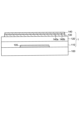
- FIG. 1 is a schematic diagram showing a laminated structure according to an embodiment of the present invention.
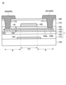
- 1 is a cross-sectional view schematically showing a thin film transistor according to an embodiment of the present invention.
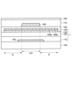
- 1 is a plan view schematically showing a thin film transistor according to an embodiment of the present invention.
- 1 is a flowchart illustrating a method for manufacturing a thin film transistor according to an embodiment of the present invention.
- 1 is a cross-sectional view showing a method for manufacturing a thin film transistor according to an embodiment of the present invention.
- 1 is a cross-sectional view showing a method for manufacturing a thin film transistor according to an embodiment of the present invention.
- 1 is a cross-sectional view showing a method for manufacturing a thin film transistor according to an embodiment of the present invention.
- 1 is a cross-sectional view showing a method for manufacturing a thin film transistor according to an embodiment of the present invention.
- 1 is a cross-sectional view showing a method for manufacturing a thin film transistor according to an embodiment of the present invention.
- 1 is a cross-sectional view showing a method for manufacturing a thin film transistor according to an embodiment of the present invention.
- 1 is a cross-sectional view showing a method for manufacturing a thin film transistor according to an embodiment of the present invention.
- 1 is a cross-sectional view showing a method for manufacturing a thin film transistor according to an embodiment of the present invention.
- 1 is a schematic diagram showing an electronic device according to an embodiment of the present invention.
- 3 is a STEM image of the vicinity of the channel region of the thin film transistor in Example A.
- 3 is a STEM image of the vicinity of the source region of the thin film transistor in Example A.
- 3 is a STEM image of the vicinity of the channel region of the thin film transistor in Comparative Example A.
- 3 is a STEM image of the vicinity of the source region of the thin film transistor in Comparative Example A.
- 3 is an EDX analysis result of Al near the channel region of the thin film transistor in Example A.
- 3 is an EDX analysis result of Al near the source region of the thin film transistor in Example A.
- 3 is a graph obtained by fitting the Al profile obtained by EDX analysis in the channel region of Example A with a Gaussian function.
- 3 is a graph obtained by fitting the Al profile obtained by EDX analysis in the source region of Example A with a Gaussian function.
- 3 is a graph obtained by fitting the Al profile obtained by EDX analysis in the channel region of Example A using a complementary error function.
- 3 is a graph obtained by fitting the Al profile obtained by EDX analysis in the source region of Example A using a complementary error function.
- 3 is a graph obtained by fitting the Al profile obtained by EDX analysis in the channel region of Example A using a Lorentz function.
- 3 is a graph obtained by fitting the Al profile obtained by EDX analysis in the source region of Example A using a Lorentz function.
- 3 is an EDX analysis result of In in the channel region of the thin film transistor in Example A.
- 3 is an EDX analysis result of In near the source region of the thin film transistor in Example A.
- the direction from the substrate toward the oxide semiconductor layer is referred to as upward. Conversely, the direction from the oxide semiconductor layer toward the substrate is referred to as downward or downward.
- the terms “upper” and “lower” are used in the description; however, for example, the substrate and the oxide semiconductor layer may be arranged so that the vertical relationship between the substrate and the oxide semiconductor layer is different from that shown in the drawings.
- the expression “an oxide semiconductor layer on a substrate” merely explains the vertical relationship between the substrate and the oxide semiconductor layer as described above; Other members may also be arranged.
- Upper or lower refers to the stacking order in a structure in which multiple layers are stacked, and when expressed as a pixel electrode above a transistor, it means a positional relationship in which the transistor and pixel electrode do not overlap in plan view. You can. On the other hand, when expressed as a pixel electrode vertically above a transistor, it means a positional relationship in which the transistor and the pixel electrode overlap in plan view.
- film and the term “layer” can be interchanged depending on the case.
- semiconductor device refers to any device that can function by utilizing semiconductor characteristics. Transistors and semiconductor circuits are one form of semiconductor devices.
- the semiconductor device in the embodiments described below may be, for example, a display device, an integrated circuit (IC) such as a microprocessor (Micro-Processing Unit: MPU), or a transistor used in a memory circuit.
- IC integrated circuit
- MPU Micro-Processing Unit
- Display device refers to a structure that displays images using an electro-optic layer.
- the term display device may refer to a display panel that includes an electro-optic layer, or may refer to a structure in which display cells are equipped with other optical components (e.g., polarizing components, backlights, touch panels, etc.).
- the "electro-optic layer” may include a liquid crystal layer, an electroluminescent (EL) layer, an electrochromic (EC) layer, and an electrophoretic layer, unless a technical contradiction arises. Therefore, the embodiments to be described later will be explained by exemplifying a liquid crystal display device including a liquid crystal layer and an organic EL display device including an organic EL layer as display devices. It can be applied to a display device including an optical layer.
- ⁇ includes A, B, or C
- ⁇ includes any one of A, B, and C
- ⁇ includes one selected from the group consisting of A, B, and C
- ⁇ includes multiple combinations of A to C, unless otherwise specified.
- these expressions do not exclude cases where ⁇ includes other elements.
- a laminated structure 1 includes a base insulating layer 11 provided on a substrate 100, a metal oxide layer 130 (MO: Metal Oxide) provided on the base insulating layer 11, An oxide semiconductor layer 140 (OS: Oxide Semiconductor) provided in contact with the metal oxide layer 130 is included.
- MO Metal Oxide
- OS Oxide Semiconductor
- a rigid substrate having light-transmitting properties is used, such as a glass substrate, a quartz substrate, and a sapphire substrate.
- a substrate containing resin such as a polyimide substrate, an acrylic substrate, a siloxane substrate, a fluororesin substrate, etc.
- impurities may be introduced into the resin in order to improve the heat resistance of the substrate 100.
- a general insulating material is used as the base insulating layer 11.
- these insulating layers may include inorganic insulating layers such as silicon oxide (SiO x ), silicon oxynitride (SiO x N y ), silicon nitride (SiN x ), silicon nitride oxide (SiN x O y ), or Laminated films are used.
- the thickness of the base insulating layer 11 is, for example, 50 nm or more and 300 nm or less, 60 nm or more and 200 nm or less, or 70 nm or more and 150 nm or less.
- SiO x N y is a silicon compound and an aluminum compound containing nitrogen (N) in a smaller proportion (x>y) than oxygen (O).
- SiN x O y is a silicon compound containing a smaller proportion of oxygen than nitrogen (x>y).
- the metal element contained in the metal oxide layer 130 is preferably a metal element that has the effect of widening the band gap of the oxide semiconductor layer 140.
- metal oxides with a band gap of 4.0 eV or more are preferable, and examples of metal elements include aluminum (Al), magnesium (Mg), calcium (Ca), scandium (Sc), and gallium ( Ga), germanium (Ge), strontium (Sr), nickel (Ni), tantalum (Ta), yttrium (Y), zirconium (Zr), barium (Ba), hafnium (Hf), cobalt (Co), and lanthanoids
- metal elements selected from the group of elements are used.
- a metal oxide layer containing aluminum as a main component may be used as the metal oxide layer 130.
- a metal oxide layer containing aluminum as a main component for example, an inorganic material such as aluminum oxide (AlO x ), aluminum oxynitride (AlO x N y ), aluminum nitride oxide (AlN x O y ), aluminum nitride (AlN x ), etc.
- An insulating layer is used.
- a metal oxide layer containing aluminum as a main component means that the proportion of aluminum contained in the metal oxide layer 130 is 1% or more of the entire metal oxide layer 130.
- the proportion of aluminum contained in the metal oxide layer 130 may be 5% or more and 70% or less, 10% or more and 60% or less, or 30% or more and 50% or less of the entire metal oxide layer 130.
- the above ratio may be a mass ratio or a weight ratio.
- the thickness of the metal oxide layer 130 is, for example, 1 nm or more and 100 nm or less, 1 nm or more and 50 nm or less, 1 nm or more and 30 nm or less, or 1 nm or more and 10 nm or less.
- the oxide semiconductor layer 140 includes indium (In) and at least one metal element (M) other than indium.
- the composition ratio of the oxide semiconductor film it is preferable that the atomic ratio of indium and at least one metal element satisfies formula (1).
- the ratio of indium to all metal elements in the oxide semiconductor film is preferably 50% or more.
- the crystal structure of the oxide semiconductor film preferably has a bixbite structure. By increasing the proportion of indium, an oxide semiconductor film having a bixbite structure can be formed.
- metal elements other than indium are not limited to one type of metal element.
- the elements other than indium may include multiple types of metal elements.
- a detailed method for manufacturing the oxide semiconductor layer 140 will be described later, but it can be formed by a sputtering method using an oxide semiconductor sputtering target.
- the composition of the oxide semiconductor layer formed by sputtering depends on the composition of the sputtering target.
- the sputtering target having the above-described composition, an oxide semiconductor layer without any deviation in the composition of metal elements can be formed by sputtering. Therefore, the composition of the metal elements (for example, indium and other metal elements) of the oxide semiconductor layer may be the same as the composition of the metal elements of the sputtering target.
- the composition of the metal element in the oxide semiconductor layer can be specified based on the composition of the metal element in the sputtering target. Note that oxygen contained in the oxide semiconductor layer changes depending on sputtering process conditions and the like, so this is not the case.
- the composition of the metal element of the oxide semiconductor layer 140 can also be specified using fluorescent X-ray analysis, electron probe micro analyzer (EPMA) analysis, or the like. Further, since the oxide semiconductor layer 140 has a polycrystalline structure, the composition of the oxide semiconductor layer 140 may be determined using an X-ray diffraction (XRD) method. Specifically, the composition of the metal element in the oxide semiconductor layer 140 can be specified based on the crystal structure and lattice constant of the oxide semiconductor layer 140 obtained by the XRD method.
- XRD X-ray diffraction
- the oxide semiconductor layer 140 according to this embodiment has a polycrystalline structure including a plurality of crystal grains. Although details will be described later, by using Poly-OS (Poly-crystalline Oxide Semiconductor) technology, the oxide semiconductor layer 140 having a novel polycrystalline structure different from conventional ones can be formed. Therefore, in order to distinguish it from the conventional oxide semiconductor layer 140 having a polycrystalline structure, the oxide semiconductor layer 140 having a polycrystalline structure according to this embodiment may be referred to as a Poly-OS film below.
- Poly-OS Poly-crystalline Oxide Semiconductor
- the crystal structure of the Poly-OS film is not particularly limited, but preferably includes a bixbite structure.
- the crystal structure of the Poly-OS film can be specified using the XRD method or the electron beam diffraction method. As described above, by increasing the proportion of indium in the oxide semiconductor layer 140, a Poly-OS film having a Bigsbyite structure can be formed.
- the oxide semiconductor layer 140 is in contact with the metal oxide layer 130. Therefore, the oxide semiconductor layer 140 may contain a metal element derived from the metal oxide layer 130. That is, the oxide semiconductor layer 140 may contain the same metal element as the metal element contained in the metal oxide layer 130. At this time, the oxide semiconductor layer 140 has a region 140a in which the metal element contained in the metal oxide layer 130 has a concentration gradient, and the concentration gradient of the metal element is between the metal oxide layer 130 and the oxide semiconductor layer 140. It is preferable that it increases as the distance approaches the interface.
- the metal element contained in the metal oxide layer 130 is a metal element that has the effect of widening the band gap.
- metal elements include aluminum (Al), magnesium (Mg), calcium (Ca), and scandium (Sc). ), gallium (Ga), germanium (Ge), strontium (Sr), nickel (Ni), tantalum (Ta), yttrium (Y), zirconium (Zr), barium (Ba), hafnium (Hf), cobalt (Co ), and one or more metal elements selected from lanthanoid elements.
- the band gap widens in the region 140a where the metal element is diffused.
- the region 140a in the oxide semiconductor layer 140 in which the metal element is diffused becomes a region that acts like an insulator.
- the oxide semiconductor layer 140 has a thickness of at least 15 nm or more, and the region 140a is a region less than 14 nm from the interface with the metal oxide layer 130 in the thickness direction of the oxide semiconductor layer 140.
- the oxide semiconductor layer 140 has a thickness of at least 15 nm or more, and the oxide semiconductor layer 140 further includes a region 140b that does not have a concentration gradient of a metal element on a side not in contact with the metal oxide layer 130. , the region 140b is in contact with the region 140a and has a thickness of 1 nm or more in the thickness direction of the oxide semiconductor layer 140. In other words, the region 140b from the surface of the oxide semiconductor layer 140 to the region 140a is a region in which the metal element does not have a concentration gradient.
- the concentration of the metal elements contained in the metal oxide layer 130 and the oxide semiconductor layer 140 can be determined by, for example, energy dispersive X-ray spectroscopy (EDX) or secondary ion mass spectrometry (SIMS). This can be confirmed by ion mass spectrometry or the like.
- the thickness of the oxide semiconductor layer 140 in the region 140a having a metal element concentration gradient can be confirmed from the metal element concentration profile obtained by EDX analysis.
- the concentration gradient of the metal elements contained in the metal oxide layer 130 and the oxide semiconductor layer 140 in the film thickness direction can be evaluated by TEM-EDX as follows.
- the laminated structure or TFT is processed by FIB (Focused Ion Beam) at an acceleration voltage of 20kV to 30kV using a composite beam processing and observation device (manufactured by JEOL Ltd., "JIB-4700F”).
- a composite beam processing and observation device manufactured by JEOL Ltd., "JIB-4700F”
- a thin film sample for cross-sectional TEM observation is picked up by a microsampling method using a focused ion beam processing and observation device (FIB) (manufactured by Hitachi High-Tech Corporation, "FB-2100") at an acceleration voltage of 40 kV.
- FIB focused ion beam processing and observation device
- a thin film sample for cross-sectional TEM observation is produced as a thin film that includes the entire area of the metal oxide layer 130 and the oxide semiconductor layer 140 in the thickness direction.
- the thin film sample for cross-sectional TEM observation is subjected to cross-sectional TEM observation, and EDX line analysis is performed on the gate insulating layer 120, metal oxide layer 130, oxide semiconductor layer 140, and gate insulating layer 150 in the film thickness direction.
- the EDX analysis is performed using an energy dispersive X-ray analyzer (manufactured by JEOL Ltd., "JED-2300T") under the following conditions. Acceleration voltage: 200kV Measurement mode: STEM mode Spot diameter: 0.16nm Measurement interval: 1nm EDX analysis uses constituent elements of the gate insulating layer 120, metal oxide layer 130, oxide semiconductor layer 140, and gate insulating layer 150 in addition to In and Al as elements to be detected (detectable elements). The concentration gradient of the metal elements in the film thickness direction is evaluated by selecting all the elements that exist and can be detected by the apparatus and performing EDX line analysis.
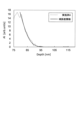
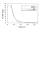
- the thickness of the region in which Al has a concentration gradient in the oxide semiconductor layer 140 may be calculated using a fitting function.
- the region 140a in which the metal element has a concentration gradient is formed by diffusion of the metal element. Since the diffusion of metal elements in a region where the metal elements have a concentration gradient is considered to have a Gaussian distribution, the profile of the metal elements can be calculated using a Gaussian function (Equation (2)) or a complementary error function (Equation (3)). Can be fitted.
- the value b is an offset value that adjusts the position of the interface between the metal oxide layer 130 and the oxide semiconductor layer 140
- the value c is a scale parameter.
- the value A is the concentration of the metal element at the interface between the metal oxide layer 130 and the oxide semiconductor layer 140.
- the thickness ⁇ d of the oxide semiconductor layer corresponding to the thickness ⁇ d of the region where the metal element has a concentration gradient can be calculated based on the value c. For example, for a Gaussian function, the distance over which the concentration of a metal element changes by approximately 99.7% can be expressed as 3c.
- the fitting function in the concentration profile of the metal element is not limited to the Gaussian function and the complementary error function.
- a Lorentz function (Equation (4)) may be used as the fitting function.
- the value A is the concentration of the metal element at the interface between the metal oxide layer 130 and the oxide semiconductor layer 140
- b is the offset value
- c is the half width at half maximum.
- a region with a thickness corresponding to c is a region that acts like an insulator.
- a region having a thickness corresponding to c corresponds to a region 140a in which the same metal element as that contained in the metal oxide layer 130 has a concentration gradient.
- the oxide semiconductor layer 140 contains indium and at least one metal element other than indium, and the metal oxide layer 130 has a region containing indium.
- Indium contained in the metal oxide layer 130 has a concentration gradient, and the concentration gradient of indium increases as it approaches the interface between the metal oxide layer 130 and the oxide semiconductor layer 140.
- FIG. 2 is a cross-sectional view schematically showing a thin film transistor 10 according to an embodiment of the present invention.
- FIG. 3 is a plan view schematically showing a thin film transistor 10 according to an embodiment of the present invention.
- the thin film transistor 10 is provided on a substrate 100.
- the thin film transistor 10 includes a gate electrode 105, gate insulating layers 110 and 120, a metal oxide layer 130, an oxide semiconductor layer 140, a gate insulating layer 150, a gate electrode 160, insulating layers 170 and 180, a source electrode 201, and a drain electrode 203. including.
- the source electrode 201 and the drain electrode 203 are not particularly distinguished, they may be collectively referred to as the source/drain electrode 200.
- the gate insulating layers 110 and 120 correspond to the base insulating layer 11 shown in FIG. 1
- the metal oxide layer 130 corresponds to the metal oxide layer 130 shown in FIG. 1
- the oxide semiconductor layer 140 corresponds to the oxide semiconductor layer 140 shown in FIG. Therefore
- the stacked structure of the gate insulating layers 110 and 120, the metal oxide layer 130, and the oxide semiconductor layer 140 corresponds to the stacked structure 1 shown in FIG. Therefore, the oxide semiconductor layer 140 has a region 140a in which the same metal element as that contained in the metal oxide layer 130 has a concentration gradient, and the concentration gradient of the metal element is different between the metal oxide layer and the oxide semiconductor layer 140. increases as one approaches the interface with
- the thin film transistor 10 includes the stacked structure 1.
- the gate electrode 105 is provided on the substrate 100. Gate insulating layer 110 and gate insulating layer 120 are provided on substrate 100 and gate electrode 105. A metal oxide layer 130 is provided over the gate insulating layer 120. Metal oxide layer 130 is in contact with gate insulating layer 120. The oxide semiconductor layer 140 is provided on the metal oxide layer 130. The oxide semiconductor layer 140 is in contact with the metal oxide layer 130. Among the main surfaces of the oxide semiconductor layer 140, the surface in contact with the metal oxide layer 130 is referred to as a lower surface 142. The end of the metal oxide layer 130 and the end of the oxide semiconductor layer 140 substantially coincide with each other.
- no semiconductor layer or oxide semiconductor layer is provided between the metal oxide layer 130 and the substrate 100.
- the sidewalls of the metal oxide layer 130 and the sidewalls of the oxide semiconductor layer 140 are aligned on a straight line, but the configuration is not limited to this.
- the angle of the sidewall of the metal oxide layer 130 with respect to the main surface of the substrate 100 may be different from the angle of the sidewall of the oxide semiconductor layer 140.
- the cross-sectional shape of the sidewall of at least one of the metal oxide layer 130 and the oxide semiconductor layer 140 may be curved.
- the gate electrode 160 faces the oxide semiconductor layer 140.
- Gate insulating layer 150 is provided between oxide semiconductor layer 140 and gate electrode 160.
- the gate insulating layer 150 is in contact with the oxide semiconductor layer 140.
- the surface in contact with the gate insulating layer 150 is referred to as an upper surface 141.
- the surface between the upper surface 141 and the lower surface 142 is referred to as a side surface 143.
- Insulating layers 170 and 180 are provided on gate insulating layer 150 and gate electrode 160.
- the insulating layers 170 and 180 are provided with openings 171 and 173 through which the oxide semiconductor layer 140 is exposed.
- the source electrode 201 is provided so as to fill the inside of the opening 171.
- the source electrode 201 is in contact with the oxide semiconductor layer 140 at the bottom of the opening 171.
- the drain electrode 203 is provided so as to fill the inside of the opening 173.
- the drain electrode 203 is in contact with the oxide semiconductor layer 140 at the bottom of the opening 173.
- the gate electrode 105 has a function as a bottom gate of the thin film transistor 10 and a function as a light shielding film for the oxide semiconductor layer 140.
- the gate insulating layer 110 has a function as a barrier film that blocks impurities that diffuse from the substrate 100 toward the oxide semiconductor layer 140.
- the gate insulating layers 110 and 120 have a function as a gate insulating layer for the bottom gate.
- the metal oxide layer 130 is a layer containing a metal oxide whose main component is aluminum, and not only improves the crystallinity of the oxide semiconductor layer 140 but also serves as a gas barrier film that blocks gases such as oxygen and hydrogen. Equipped with functions.
- the oxide semiconductor layer 140 is divided into a source region S, a drain region D, and a channel region CH.
- the channel region CH is a region of the oxide semiconductor layer 140 that is vertically below the gate electrode 160.
- the source region S is a region of the oxide semiconductor layer 140 that does not overlap with the gate electrode 160 and is a region closer to the source electrode 201 than the channel region CH.
- the drain region D is a region of the oxide semiconductor layer 140 that does not overlap with the gate electrode 160 and is a region closer to the drain electrode 203 than the channel region CH.
- the oxide semiconductor layer 140 in the channel region CH has physical properties as a semiconductor.
- the oxide semiconductor layer 140 in the source region S and drain region D has physical properties as a conductor.
- the gate electrode 160 has a function as a light shielding film for the top gate of the thin film transistor 10 and the oxide semiconductor layer 140.
- the gate insulating layer 150 has a function as a gate insulating layer for the top gate, and has a function of releasing oxygen through heat treatment in the manufacturing process.
- the insulating layers 170 and 180 have the function of insulating the gate electrode 160 and the source/drain electrode 200 and reducing the parasitic capacitance between them.
- the operation of the thin film transistor 10 is mainly controlled by the voltage supplied to the gate electrode 160.
- An auxiliary voltage is supplied to the gate electrode 105.
- the gate electrode 105 is simply used as a light shielding film, a specific voltage may not be supplied to the gate electrode 105, and the gate electrode 105 may be floating. In other words, the gate electrode 105 may simply be called a "light shielding film".
- the oxide semiconductor layer 140 has a thickness of at least 15 nm or more.
- a region 140a in which the same metal element as that contained in the metal oxide layer 130 has a concentration gradient is located from the interface with the metal oxide layer 130 in the thickness direction of the oxide semiconductor layer 140. This is a region of less than 14 nm.
- the region 140a is a region that is difficult to crystallize immediately after the oxide semiconductor layer 140 is formed due to the influence of the metal oxide layer 130. Further, the metal element contained in the metal oxide layer 130 has the effect of widening the band gap of the oxide semiconductor layer 140.
- a region 140b extending 1 nm or more from the surface of the oxide semiconductor layer 140 is a region in which the metal element does not have a concentration gradient.
- the oxide semiconductor layer 140 can have a different band gap between the region 140b (front channel side) near the gate electrode 160 and the region 140a (back channel side) near the metal oxide layer 130.
- the volume density of carriers increases by limiting the region where free carriers are generated by applying a voltage to the gate electrode of the transistor to the region 140b, the volume density of free carriers increases and the mobility increases.
- the oxide semiconductor layer 140 also has high mobility.
- the mobility in this specification and the like refers to the field effect mobility in the saturation region of the thin film transistor 10, and is the value obtained by subtracting the threshold voltage (Vth) of the thin film transistor 10 from the voltage (Vg) supplied to the gate electrode ( Vg ⁇ Vth) means the maximum value of field effect mobility in a region where the potential difference (Vd) between the source electrode and the drain electrode is smaller.
- the oxide semiconductor layer 140 contains indium and at least one or more metal elements other than indium, and the metal oxide layer 130 has a region containing indium.
- Indium contained in the metal oxide layer 130 has a concentration gradient, and the concentration gradient of indium increases as it approaches the interface between the metal oxide layer 130 and the oxide semiconductor layer 140.
- a dual-gate transistor in which the gate electrode is provided both above and below the oxide semiconductor layer 140 is used as the thin film transistor 10.
- the present invention is not limited to this structure.
- a top-gate transistor in which a gate electrode is provided only above the oxide semiconductor layer 140 may be used as the thin film transistor 10.
- the above configuration is just one embodiment, and the present invention is not limited to the above configuration.
- the planar pattern of the metal oxide layer 130 is substantially the same as the planar pattern of the oxide semiconductor layer 140 in plan view.
- a lower surface 142 of the oxide semiconductor layer 140 is covered with a metal oxide layer 130.
- the entire lower surface 142 of the oxide semiconductor layer 140 is covered with the metal oxide layer 130.
- the width of the gate electrode 105 is larger than the width of the gate electrode 160.
- the D1 direction is a direction that connects the source electrode 201 and the drain electrode 203, and is a direction that indicates the channel length L of the thin film transistor 10.
- the length of the region (channel region CH) where the oxide semiconductor layer 140 and the gate electrode 160 overlap in the D1 direction is the channel length L
- the width of the channel region CH in the D2 direction is the channel width W. be.
- a configuration in which the entire lower surface 142 of the oxide semiconductor layer 140 is covered with the metal oxide layer 130 is illustrated, but the configuration is not limited to this.
- a portion of the lower surface 142 of the oxide semiconductor layer 140 does not need to be in contact with the metal oxide layer 130.
- the entire lower surface 142 of the oxide semiconductor layer 140 in the channel region CH is covered with the metal oxide layer 130, and all or part of the lower surface 142 of the oxide semiconductor layer 140 in the source region S and the drain region D is covered with metal oxide. It may not be covered by the material layer 130. That is, all or part of the lower surface 142 of the oxide semiconductor layer 140 in the source region S and drain region D does not need to be in contact with the metal oxide layer 130.
- a part of the lower surface 142 of the oxide semiconductor layer 140 in the channel region CH is not covered with the metal oxide layer 130, and the other part of the lower surface 142 is in contact with the metal oxide layer 130. You can leave it there.
- Gate insulating layer 150 may be patterned.
- the gate insulating layer 150 may be patterned so that not only the top surface of the oxide semiconductor layer 140 but also the side surfaces of the oxide semiconductor layer 140 are exposed.
- FIG. 3 illustrates a configuration in which the source/drain electrodes 200 do not overlap the gate electrodes 105 and 160 in plan view
- the present invention is not limited to this configuration.
- the source/drain electrode 200 may overlap with at least one of the gate electrodes 105 and 160 in plan view.
- the above configuration is just one embodiment, and the present invention is not limited to the above configuration.
- the material of the substrate 100 described in the laminated structure 1 can be applied.
- the substrate 100 does not need to be transparent, so an impurity that reduces the transparency of the substrate 100 may be used.
- the substrate 100 may be a semiconductor substrate such as a silicon substrate, a silicon carbide substrate, or a compound semiconductor substrate, or a conductive substrate such as a stainless steel substrate, which does not have light-transmitting properties. used.
- General metal materials are used for the gate electrode 105, the gate electrode 160, and the source/drain electrodes 200.
- these materials include aluminum (Al), titanium (Ti), chromium (Cr), cobalt (Co), nickel (Ni), molybdenum (Mo), hafnium (Hf), tantalum (Ta), and tungsten (W). ), bismuth (Bi), silver (Ag), copper (Cu), or alloys or compounds thereof.
- the above materials may be used in a single layer or in a stacked layer.
- the material of the base insulating layer 11 described in the stacked structure 1 can be applied.
- a common insulating material is used for the insulating layers 170 and 180.
- inorganic insulating layers such as silicon oxide (SiO x ), silicon oxynitride (SiO x N y ), silicon nitride (SiN x ), or silicon nitride oxide (SiN x O y ) are used. .
- the above materials may be used in a single layer or in a laminated manner.
- an insulating layer containing oxygen among the above insulating layers is used.
- an inorganic insulating layer such as silicon oxide (SiO x ) or silicon oxynitride (SiO x N y ) is used.
- the gate insulating layer 120 it is preferable to use an insulating layer that has a function of releasing oxygen through heat treatment.
- the temperature of the heat treatment at which the gate insulating layer 120 releases oxygen is, for example, 600° C. or less, 500° C. or less, 450° C. or less, or 400° C. or less. That is, the gate insulating layer 120 releases oxygen at a heat treatment temperature performed in the manufacturing process of the thin film transistor 10 when a glass substrate is used as the substrate 100, for example.
- the gate insulating layer 150 it is preferable to use an insulating layer with few defects.
- the gate insulating layer The oxygen composition ratio in 150 is closer to the stoichiometric ratio for the insulating layer than the oxygen composition ratio in the other insulating layer.
- silicon oxide ( SiOx ) is used for each of the gate insulating layer 150 and the insulating layer 180
- the composition ratio of oxygen in the silicon oxide used as the gate insulating layer 150 is the same as that of the oxide used as the insulating layer 180.
- a layer in which no defects are observed when evaluated by electron spin resonance (ESR) may be used as the gate insulating layer 150.
- the material of the metal oxide layer 130 explained in the laminated structure 1 can be applied.
- a metal oxide containing aluminum as a main component is used.
- an inorganic insulating layer such as aluminum oxide (AlO x ), aluminum oxynitride (AlO x N y ), aluminum nitride oxide (AlN x O y ), or aluminum nitride (AlN x ) is used, for example. .
- AlO x aluminum oxide
- AlO x N y aluminum oxynitride
- AlN x O y aluminum nitride oxide
- AlN x aluminum nitride
- a metal oxide layer containing aluminum as a main component means that the ratio of aluminum contained in the metal oxide layer 130 is 1% or more of the entire metal oxide layer 130.
- the proportion of aluminum contained in the metal oxide layer 130 may be 5% or more and 70% or less, 10% or more and 60% or less, or 30% or more and 50% or less of the entire metal oxide
- an oxide semiconductor layer having crystallinity can be used as the oxide semiconductor layer 140. Oxygen vacancies are less likely to be formed in a crystalline oxide semiconductor than in an amorphous oxide semiconductor.
- FIG. 4 is a flowchart showing a method for manufacturing the laminated structure 1 and the thin film transistor 10 according to an embodiment of the present invention.
- 5 to 12 are cross-sectional views illustrating a method for manufacturing the laminated structure 1 and thin film transistor 10 according to an embodiment of the present invention.
- a gate electrode 105 is formed as a bottom gate on the substrate 100, and gate insulating layers 110 and 120 are formed on the gate electrode 105.
- GI/GE formation For example, silicon nitride is formed as the gate insulating layer 110.
- silicon oxide is formed as the gate insulating layer 120.
- the gate insulating layers 110 and 120 are formed by a CVD (Chemical Vapor Deposition) method.
- the gate insulating layer 110 can block impurities that diffuse toward the oxide semiconductor layer 140 from the substrate 100 side, for example.
- the silicon oxide used as the gate insulating layer 120 is a physical silicon oxide that releases oxygen by heat treatment.
- a metal oxide layer 130 and an oxide semiconductor layer 140 are formed on the gate insulating layer 120 ("OS/MO film formation" in step S3002 in FIG. 4).
- the metal oxide layer 130 is formed by sputtering or atomic layer deposition (ALD).
- the thickness of the metal oxide layer 130 is, for example, 1 nm or more and 100 nm or less, 1 nm or more and 50 nm or less, 1 nm or more and 30 nm or less, or 1 nm or more and 10 nm or less.
- aluminum oxide is used as the metal oxide layer 130.
- Aluminum oxide has high gas barrier properties.
- aluminum oxide used as the metal oxide layer 130 blocks hydrogen and oxygen released from the gate insulating layer 120 and prevents the released hydrogen and oxygen from reaching the oxide semiconductor layer 140. suppress.
- an oxide semiconductor layer 140 is formed on the metal oxide layer 130.
- the thickness of the oxide semiconductor layer 140 is, for example, 15 nm or more and 100 nm or less, 15 nm or more and 70 nm or less, or 15 nm or more and 40 nm or less.
- the thickness of the oxide semiconductor layer 140 is preferably at least 15 nm or more.
- the oxide semiconductor layer 140 after film formation and before OS annealing is preferably a film with a small amount of crystalline components; It is particularly preferable that the amount of components is low.
- the conditions for forming the oxide semiconductor layer 140 are preferably such that the oxide semiconductor layer 140 immediately after being formed does not crystallize as much as possible.
- the oxide semiconductor layer be formed while controlling the substrate temperature.
- the substrate temperature is, for example, 100°C or lower, preferably 70°C or lower, and more preferably 50°C or lower.
- the substrate temperature may be 30° C. or lower.
- Substrate temperature can be controlled, for example, by cooling the substrate.
- the oxide semiconductor layer may be deposited at a deposition rate that does not cause the substrate temperature to exceed a predetermined temperature.
- the substrate temperature may be controlled by increasing the distance between the target and the substrate so that the substrate is not affected by the sputtering target.
- the oxide semiconductor layer is formed under conditions where the oxygen partial pressure is 10% or less.
- the oxygen partial pressure is, for example, greater than 2% and less than or equal to 20%, preferably greater than or equal to 3% and less than or equal to 15%, and more preferably greater than or equal to 3% and less than or equal to 10%. Note that when the oxide semiconductor layer is formed under conditions where the oxygen partial pressure is 2% or less, the oxide semiconductor layer is not crystallized even if an annealing process is performed.
- a pattern of the oxide semiconductor layer 140 is formed ("OS pattern formation" in step S3003 in FIG. 4).
- a resist mask is formed over the oxide semiconductor layer 140, and the oxide semiconductor layer 140 is etched using the resist mask.
- Wet etching may be used to etch the oxide semiconductor layer 140, or dry etching may be used.
- Wet etching can be performed using an acidic etchant.
- the etchant for example, oxalic acid, PAN, sulfuric acid, hydrogen peroxide, or hydrofluoric acid can be used.
- oxide semiconductor layer 140 After patterning the oxide semiconductor layer 140, heat treatment (OS annealing) is performed on the oxide semiconductor layer 140 ("OS annealing" in step S3004 in FIG. 4). In this embodiment, the oxide semiconductor layer 140 is crystallized by this OS annealing.
- the oxide semiconductor layer 140 is held at a predetermined temperature for a predetermined time.
- the predetermined attained temperature is 300°C or more and 500°C or less, preferably 350°C or more and 450°C or less.
- the holding time at the final temperature is 15 minutes or more and 120 minutes or less, preferably 30 minutes or more and 60 minutes or less.
- the metal element contained in the metal oxide layer 130 is diffused into the oxide semiconductor layer 140 in the process of crystallizing the oxide semiconductor layer 140.
- the oxide semiconductor layer 140 has a region 140a in which the same metal element as that contained in the metal oxide layer has a concentration gradient, and the concentration gradient of the metal element is different between the metal oxide layer and the oxide semiconductor layer 140. increases as one approaches the interface with
- the metal element contained in the metal oxide layer 130 is a metal element that has the effect of widening the band gap.
- the band gap widens in the region 140a where the metal element is diffused.
- the region 140a in the oxide semiconductor layer 140 in which the metal element is diffused becomes a region that acts like an insulator.
- the oxide semiconductor layer 140 has a region 140a in which the same metal element as that contained in the metal oxide layer 130 has a concentration gradient. ing. Further, the concentration gradient of the metal element increases as it approaches the interface between the metal oxide layer 130 and the oxide semiconductor layer 140.
- the oxide semiconductor layer 140 has a thickness of at least 15 nm or more.
- a region 140a in which the same metal element as that contained in the metal oxide layer 130 has a concentration gradient is located from the interface with the metal oxide layer 130 in the thickness direction of the oxide semiconductor layer 140. This is a region of less than 14 nm.
- the region 140a is a region that is difficult to crystallize immediately after the oxide semiconductor layer 140 is formed due to the influence of the metal oxide layer 130. Further, the metal element contained in the metal oxide layer 130 has the effect of widening the band gap of the oxide semiconductor layer 140. Therefore, in the oxide semiconductor layer, the region 140a in which the metal element has a concentration gradient can be a region that acts as an insulator.
- the oxide semiconductor layer 140 When forming the oxide semiconductor layer, it can be formed to a thickness of 15 nm or more. Therefore, in the annealing process, the oxide semiconductor layer 140 can be favorably crystallized. That is, after the oxide semiconductor layer 140 is formed to a thickness that allows crystallization, the metal element contained in the metal oxide layer 130 is diffused into the oxide semiconductor layer 140 in an annealing process. Thereby, a region 140a that acts as an insulator can be formed in the oxide semiconductor layer 140. Therefore, in the oxide semiconductor layer 140, the thickness of the region 140b that acts as a semiconductor can be substantially reduced.
- a region 140b from the surface of the oxide semiconductor layer 140 to the region 140a is a region in which the metal element does not have a concentration gradient.
- the oxide semiconductor layer 140 can have a different band gap between the region 140b (front channel side) near the gate electrode 160 and the region 140a (back channel side) near the metal oxide layer 130. .
- the oxide semiconductor layer 140 can concentrate free carriers in the region 140b near the gate electrode 160. Therefore, the field effect mobility of the thin film transistor 10 can be improved. Therefore, in the stacked structure 1 according to the embodiment of the present invention, it is presumed that the oxide semiconductor layer 140 also has high mobility.
- indium contained in the oxide semiconductor layer 140 may be diffused into the metal oxide layer 130.
- the metal oxide layer 130 has a region containing indium.
- Indium contained in the metal oxide layer 130 has a concentration gradient, and the concentration gradient of indium increases as it approaches the interface between the metal oxide layer 130 and the oxide semiconductor layer 140.
- a pattern of the metal oxide layer 130 is formed ("MO pattern formation" in step S3005 in FIG. 4).
- the metal oxide layer 130 is etched using the oxide semiconductor layer 140 patterned in the above process as a mask.
- Wet etching or dry etching may be used to etch the metal oxide layer 130.
- diluted hydrofluoric acid (DHF) is used for wet etching.
- the laminated structure 1 shown in FIG. 1 can be manufactured. Note that in the method for manufacturing the laminated structure 1, the step of forming the pattern of the metal oxide layer 130 may be omitted.
- the thin film transistor 10 is manufactured using the stacked structure 1 described above.
- a gate insulating layer 150 is formed ("GI formation" in step S3006 in FIG. 4).
- silicon oxide is formed as the gate insulating layer 150.
- Gate insulating layer 150 is formed by a CVD method.
- the gate insulating layer 150 may be formed at a film forming temperature of 350° C. or higher.
- the thickness of the gate insulating layer 150 is, for example, 50 nm or more and 300 nm or less, 60 nm or more and 200 nm or less, or 70 nm or more and 150 nm or less.
- a gate electrode 160 is formed ("GE formation" in step S3008 in FIG. 4).
- the gate electrode 160 is formed by a sputtering method or an atomic layer deposition method, and is patterned through a photolithography process.
- the resistance of the source region S and drain region D of the oxide semiconductor layer 140 is reduced (“SD resistance reduction” in step S3009 in FIG. 4).
- impurities are implanted into the oxide semiconductor layer 140 from the gate electrode 160 side through the gate insulating layer 150 by ion implantation.
- argon (Ar), phosphorus (P), and boron (B) are implanted into the oxide semiconductor layer 140 by ion implantation.
- Oxygen vacancies are formed in the oxide semiconductor layer 140 by ion implantation, so that the resistance of the oxide semiconductor layer 140 is reduced. Since the gate electrode 160 is provided above the oxide semiconductor layer 140 functioning as the channel region CH of the thin film transistor 10, no impurity is implanted into the oxide semiconductor layer 140 in the channel region CH.
- insulating layers 170 and 180 are formed as interlayer films on the gate insulating layer 150 and the gate electrode 160 ("interlayer film formation" in step S3010 in FIG. 4).
- Insulating layers 170 and 180 are formed by CVD.
- silicon nitride is formed as the insulating layer 170
- silicon oxide is formed as the insulating layer 180.
- the materials used for the insulating layers 170 and 180 are not limited to those described above.
- the thickness of the insulating layer 170 is 50 nm or more and 500 nm or less.
- the thickness of the insulating layer 180 is 50 nm or more and 500 nm or less.
- openings 171 and 173 are formed in the gate insulating layer 150 and the insulating layers 170 and 180 ("contact opening” in step S3011 in FIG. 4).
- the oxide semiconductor layer 140 in the source region S is exposed through the opening 171.
- the oxide semiconductor layer 140 in the drain region D is exposed through the opening 173.
- the source/drain electrodes 200 are formed on the oxide semiconductor layer 140 exposed by the openings 171 and 173 and on the insulating layer 180 ("SD formation" in step S3012 in FIG. 4), the electrodes shown in FIG. 2 are formed.
- Thin film transistor 10 is completed.
- the thickness of the oxide semiconductor layer functioning as a channel can be substantially reduced.
- the mobility is 30 cm 2 /Vs or more, 35 cm 2 /Vs or more, and 40 cm 2 /Vs or more, or 50 cm 2 /Vs or more can be obtained.
- FIG. 13 is a schematic diagram showing an electronic device 1000 according to an embodiment of the present invention. Specifically, FIG. 13 shows a smartphone that is an example of the electronic device 1000.
- Electronic device 1000 includes a display device 1100 with curved sides.
- the display device 1100 includes a plurality of pixels for displaying images, and the plurality of pixels are controlled by a pixel circuit, a driving circuit, and the like.
- the pixel circuit and the drive circuit include the thin film transistor 10 described in the second embodiment. Since the thin film transistor 10 has high field effect mobility, it can improve the responsiveness of the pixel circuit and the drive circuit, and as a result, the performance of the electronic device 1000 can be improved.
- the electronic device 1000 is not limited to a smartphone.
- the electronic device 1000 includes, for example, a watch, a tablet, a notebook computer, a car navigation system, or an electronic device having a display device such as a television.
- the oxide semiconductor layer described in the first embodiment or the thin film transistor 10 described in the second embodiment can be applied to any electronic device, regardless of whether or not it includes a display device.
- a thin film transistor 10 according to an embodiment of the present invention was manufactured, and the results of verifying the concentration of metal elements in the oxide semiconductor layer 140 and the metal oxide layer 130 will be described.
- Example A As Example A, a thin film transistor 10 according to an embodiment of the present invention was manufactured.
- the thin film transistor 10 was manufactured according to the sequence diagram shown in FIG. Here, a glass substrate was used as the substrate, a silicon nitride film was used as the gate insulating layer 110, and a silicon oxide film was used as the gate insulating layer 120. Further, as the metal oxide layer 130, a 10 nm thick aluminum oxide layer was used.
- the oxide semiconductor layer 140 an oxide semiconductor was used in which the atomic ratio of indium to all metal elements contained in the film was 70% and had a polycrystalline structure of 30 nm.
- a silicon oxide film was used as the gate insulating layer 150.
- Comparative example A As a comparative example, a thin film transistor without the metal oxide layer 130 was manufactured.
- the thin film transistor of Comparative Example A was manufactured according to the sequence diagram shown in FIG. 3 except that the metal oxide layer 130 was not formed. That is, the steps of MO film formation in step S3003 and MO pattern formation in step S3005 are omitted. Other configurations, film thickness, film forming conditions, etc. are the same as in Example A.
- FIG. 14 is a STEM image of the vicinity of the channel region of the thin film transistor in Example A
- FIG. 15 is a STEM image of the vicinity of the source region of the thin film transistor in Example A
- 16 is a STEM image of the vicinity of the channel region of the thin film transistor in Comparative Example A
- FIG. 17 is a STEM image of the vicinity of the source region of the thin film transistor in Comparative Example A.
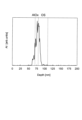
- FIG. 18 shows the EDX analysis results of Al near the channel region of the thin film transistor in Example A.
- FIG. 19 is an EDX analysis result of Al near the source region of the thin film transistor in Example A.
- the depth of the interface between the aluminum oxide layer and the oxide semiconductor layer is approximately 80 nm.
- the interface between the aluminum oxide layer and the oxide semiconductor layer is indicated by a dotted line.
- the thickness of the aluminum oxide layer and the thickness of the oxide semiconductor layer are indicated by dotted lines with 80 nm as a reference.
- Al has a concentration gradient in the channel region and source region of the thin film transistor in Example A.
- the region where Al has a concentration gradient is a region less than 15 nm from the interface with the metal oxide layer 130 in the thickness direction of the oxide semiconductor layer 140.
- a region approximately 15 nm from the surface of the oxide semiconductor layer 140 is a region where Al does not have a concentration gradient.
- Example A the Al profile obtained by EDX analysis was fitted with the Gaussian function shown in equation (2), the complementary error function shown in equation (3), and the Lorentzian function shown in equation (4). Explain the results.
- FIG. 20 is a graph obtained by fitting the Al profile obtained by EDX analysis in the channel region of Example A with a Gaussian function.
- FIG. 21 is a graph obtained by fitting the Al profile obtained by EDX analysis in the source region of Example A with a Gaussian function.
- FIG. 22 is a graph obtained by fitting the Al profile obtained by EDX analysis in the channel region of Example A using a complementary error function.
- FIG. 23 is a graph obtained by fitting the Al profile obtained by EDX analysis in the source region of Example A using a complementary error function.
- FIG. 24 is a graph obtained by fitting the Al profile obtained by EDX analysis in the channel region of Example A using a Lorentz function.
- FIG. 25 is a graph obtained by fitting the Al profile obtained by EDX analysis in the source region of Example A using a Lorentz function.
- Example A the fitting function in Example A is shown by a solid line.
- the positive direction of the distance is the direction from the interface between the metal oxide layer 130 and the oxide semiconductor layer 140 toward the oxide semiconductor layer 140
- the negative direction of the distance is the direction from the interface between the metal oxide layer 130 and the oxide semiconductor layer 140. This is the direction from the interface toward the metal oxide layer 130.
- Table 1 shows the value c (scale parameter or half width at half maximum) calculated by fitting the Al concentration in each of the channel region and the source region using each fitting function.
- the thickness ⁇ d of the region having an Al concentration gradient in the oxide semiconductor layer 140 of Example A was 12 nm.
- a region having a thickness of up to 4 nm from the interface between the metal oxide layer 130 and the oxide semiconductor layer 140 corresponds to the region 140a.
- a region 5 nm or more from the interface between the metal oxide layer 130 and the oxide semiconductor layer 140 is a region that acts as a semiconductor.
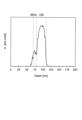
- FIG. 26 shows the EDX analysis results of In in the channel region of the thin film transistor in Example A.
- FIG. 27 shows the EDX analysis results of In near the source region of the thin film transistor in Example A.
- the depth of the interface between the aluminum oxide layer and the oxide semiconductor layer in Example A is approximately 80 nm.
- the interface between the aluminum oxide layer and the oxide semiconductor layer is indicated by a dotted line.
- the thickness of the aluminum oxide layer and the thickness of the oxide semiconductor layer are indicated by dotted lines with 80 nm as a reference.
- the metal oxide layer 130 contains In, which is included in the oxide semiconductor layer 140. It can be seen that In contained in the metal oxide layer 130 has a concentration gradient, and the In concentration gradient increases as it approaches the interface between the metal oxide layer 130 and the oxide semiconductor layer 140.
- the oxide semiconductor layer has a region in which the same metal element as that contained in the metal oxide layer has a concentration gradient, and has the characteristic that it increases as it approaches the interface between the metal oxide layer and the oxide semiconductor layer.
- the oxide semiconductor layer can be well crystallized and the thickness that functions as a channel can be substantially reduced.
- the carrier concentration can be increased in the region functioning as a channel. Therefore, it is considered that the field effect mobility of the thin film transistor can be significantly increased.
- 1 Laminated structure, 10: Thin film transistor, 11: Base insulating layer, 100: Substrate, 105, 160: Gate electrode, 110, 120, 150: Gate insulating layer, 130: Metal oxide layer, 140: Oxide semiconductor layer , 140a: region, 140b: region, 141: top surface, 142: bottom surface, 143: side surface, 170, 180: insulating layer, 171, 173: opening, 200: source/drain electrode, 201: source electrode, 203: drain electrode , 1000: Electronic equipment, 1100: Display device
Landscapes
- Chemical & Material Sciences (AREA)
- Chemical Kinetics & Catalysis (AREA)
- Engineering & Computer Science (AREA)
- Materials Engineering (AREA)
- Mechanical Engineering (AREA)
- Metallurgy (AREA)
- Organic Chemistry (AREA)
- Thin Film Transistor (AREA)
Priority Applications (5)
| Application Number | Priority Date | Filing Date | Title |
|---|---|---|---|
| CN202380055153.3A CN119604968A (zh) | 2022-08-01 | 2023-07-26 | 层叠结构体及薄膜晶体管 |
| DE112023002495.2T DE112023002495T5 (de) | 2022-08-01 | 2023-07-26 | Laminierte struktur und dünnschichttransistor |
| KR1020257001779A KR20250026275A (ko) | 2022-08-01 | 2023-07-26 | 적층 구조체 및 박막 트랜지스터 |
| JP2024539107A JPWO2024029429A1 (https=) | 2022-08-01 | 2023-07-26 | |
| US19/039,202 US20250176220A1 (en) | 2022-08-01 | 2025-01-28 | Laminated structure and thin film transistor |
Applications Claiming Priority (2)
| Application Number | Priority Date | Filing Date | Title |
|---|---|---|---|
| JP2022-122911 | 2022-08-01 | ||
| JP2022122911 | 2022-08-01 |
Related Child Applications (1)
| Application Number | Title | Priority Date | Filing Date |
|---|---|---|---|
| US19/039,202 Continuation US20250176220A1 (en) | 2022-08-01 | 2025-01-28 | Laminated structure and thin film transistor |
Publications (1)
| Publication Number | Publication Date |
|---|---|
| WO2024029429A1 true WO2024029429A1 (ja) | 2024-02-08 |
Family
ID=89848999
Family Applications (1)
| Application Number | Title | Priority Date | Filing Date |
|---|---|---|---|
| PCT/JP2023/027457 Ceased WO2024029429A1 (ja) | 2022-08-01 | 2023-07-26 | 積層構造体及び薄膜トランジスタ |
Country Status (7)
| Country | Link |
|---|---|
| US (1) | US20250176220A1 (https=) |
| JP (1) | JPWO2024029429A1 (https=) |
| KR (1) | KR20250026275A (https=) |
| CN (1) | CN119604968A (https=) |
| DE (1) | DE112023002495T5 (https=) |
| TW (1) | TWI858841B (https=) |
| WO (1) | WO2024029429A1 (https=) |
Citations (5)
| Publication number | Priority date | Publication date | Assignee | Title |
|---|---|---|---|---|
| JP2011228695A (ja) * | 2010-04-02 | 2011-11-10 | Semiconductor Energy Lab Co Ltd | 半導体装置 |
| WO2013021632A1 (ja) * | 2011-08-11 | 2013-02-14 | 出光興産株式会社 | 薄膜トランジスタ |
| JP2013102158A (ja) * | 2011-10-21 | 2013-05-23 | Semiconductor Energy Lab Co Ltd | 半導体装置およびその作製方法 |
| WO2014136612A1 (ja) * | 2013-03-07 | 2014-09-12 | シャープ株式会社 | 半導体装置およびその製造方法 |
| JP2017126693A (ja) * | 2016-01-15 | 2017-07-20 | 株式会社ジャパンディスプレイ | 半導体装置 |
Family Cites Families (7)
| Publication number | Priority date | Publication date | Assignee | Title |
|---|---|---|---|---|
| US8871565B2 (en) | 2010-09-13 | 2014-10-28 | Semiconductor Energy Laboratory Co., Ltd. | Method for manufacturing semiconductor device |
| EP2880690B1 (en) | 2012-08-03 | 2019-02-27 | Semiconductor Energy Laboratory Co. Ltd. | Semiconductor device with oxide semiconductor stacked film |
| TWI761605B (zh) | 2012-09-14 | 2022-04-21 | 日商半導體能源研究所股份有限公司 | 半導體裝置及其製造方法 |
| KR102220279B1 (ko) | 2012-10-19 | 2021-02-24 | 가부시키가이샤 한도오따이 에네루기 켄큐쇼 | 산화물 반도체막을 포함하는 다층막 및 반도체 장치의 제작 방법 |
| US9425217B2 (en) | 2013-09-23 | 2016-08-23 | Semiconductor Energy Laboratory Co., Ltd. | Semiconductor device |
| CN109121438B (zh) | 2016-02-12 | 2022-02-18 | 株式会社半导体能源研究所 | 半导体装置以及包括该半导体装置的显示装置 |
| US10845704B2 (en) * | 2018-10-30 | 2020-11-24 | Taiwan Semiconductor Manufacturing Co., Ltd. | Extreme ultraviolet photolithography method with infiltration for enhanced sensitivity and etch resistance |
-
2023
- 2023-07-26 CN CN202380055153.3A patent/CN119604968A/zh active Pending
- 2023-07-26 KR KR1020257001779A patent/KR20250026275A/ko active Pending
- 2023-07-26 JP JP2024539107A patent/JPWO2024029429A1/ja active Pending
- 2023-07-26 DE DE112023002495.2T patent/DE112023002495T5/de active Pending
- 2023-07-26 WO PCT/JP2023/027457 patent/WO2024029429A1/ja not_active Ceased
- 2023-08-01 TW TW112128779A patent/TWI858841B/zh active
-
2025
- 2025-01-28 US US19/039,202 patent/US20250176220A1/en active Pending
Patent Citations (5)
| Publication number | Priority date | Publication date | Assignee | Title |
|---|---|---|---|---|
| JP2011228695A (ja) * | 2010-04-02 | 2011-11-10 | Semiconductor Energy Lab Co Ltd | 半導体装置 |
| WO2013021632A1 (ja) * | 2011-08-11 | 2013-02-14 | 出光興産株式会社 | 薄膜トランジスタ |
| JP2013102158A (ja) * | 2011-10-21 | 2013-05-23 | Semiconductor Energy Lab Co Ltd | 半導体装置およびその作製方法 |
| WO2014136612A1 (ja) * | 2013-03-07 | 2014-09-12 | シャープ株式会社 | 半導体装置およびその製造方法 |
| JP2017126693A (ja) * | 2016-01-15 | 2017-07-20 | 株式会社ジャパンディスプレイ | 半導体装置 |
Non-Patent Citations (1)
| Title |
|---|
| MIYAZAKI TORU: "The Formation of Microstructure in Materials and Its Theoretical Basis (IV) ~The Formation Process of Microstructure Based on Interdiffusion~", MATERIA JAPAN, NIHON KINZOKU GAKKAI, SENDAI, JP, vol. 53, no. 11, 1 January 2014 (2014-01-01), JP , pages 550 - 557, XP093134671, ISSN: 1340-2625, DOI: 10.2320/materia.53.550 * |
Also Published As
| Publication number | Publication date |
|---|---|
| KR20250026275A (ko) | 2025-02-25 |
| JPWO2024029429A1 (https=) | 2024-02-08 |
| DE112023002495T5 (de) | 2025-04-10 |
| US20250176220A1 (en) | 2025-05-29 |
| TWI858841B (zh) | 2024-10-11 |
| TW202408020A (zh) | 2024-02-16 |
| CN119604968A (zh) | 2025-03-11 |
Similar Documents
| Publication | Publication Date | Title |
|---|---|---|
| US20240113227A1 (en) | Semiconductor device | |
| WO2024029429A1 (ja) | 積層構造体及び薄膜トランジスタ | |
| KR102733354B1 (ko) | 반도체 장치의 제조 방법 | |
| KR102944325B1 (ko) | 박막 트랜지스터 및 전자 기기 | |
| US20250113543A1 (en) | Semiconductor device | |
| US12610624B2 (en) | Method for manufacturing semiconductor device | |
| KR102944004B1 (ko) | 산화물 반도체막, 박막 트랜지스터 및 전자 기기 | |
| KR102944064B1 (ko) | 박막 트랜지스터 및 전자 기기 | |
| US12598816B2 (en) | Method for manufacturing semiconductor device | |
| US20250048680A1 (en) | Semiconductor device | |
| US20250176222A1 (en) | Oxide semiconductor film, thin film transistor, and electronic device | |
| US20240312999A1 (en) | Semiconductor device | |
| US20250022966A1 (en) | Semiconductor device | |
| US20250022965A1 (en) | Semiconductor device | |
| US20240113228A1 (en) | Semiconductor device and method for manufacturing semiconductor device | |
| US20250380465A1 (en) | Semiconductor device and manufacturing method thereof | |
| US20240021668A1 (en) | Semiconductor device | |
| US20250063761A1 (en) | Semiconductor device | |
| US20250113542A1 (en) | Semiconductor device | |
| US20250294813A1 (en) | Semiconductor device | |
| US20260006828A1 (en) | Semiconductor device and manufacturing method thereof | |
| US20240097043A1 (en) | Semiconductor device | |
| WO2023189550A1 (ja) | 半導体装置 | |
| WO2023189487A1 (ja) | 半導体装置 | |
| WO2023189549A1 (ja) | 半導体装置及び半導体装置の製造方法 |
Legal Events
| Date | Code | Title | Description |
|---|---|---|---|
| 121 | Ep: the epo has been informed by wipo that ep was designated in this application |
Ref document number: 23849984 Country of ref document: EP Kind code of ref document: A1 |
|
| WWE | Wipo information: entry into national phase |
Ref document number: 2024539107 Country of ref document: JP |
|
| ENP | Entry into the national phase |
Ref document number: 20257001779 Country of ref document: KR Kind code of ref document: A |
|
| WWE | Wipo information: entry into national phase |
Ref document number: 1020257001779 Country of ref document: KR |
|
| WWE | Wipo information: entry into national phase |
Ref document number: 202380055153.3 Country of ref document: CN |
|
| WWE | Wipo information: entry into national phase |
Ref document number: 202517006908 Country of ref document: IN |
|
| WWE | Wipo information: entry into national phase |
Ref document number: 112023002495 Country of ref document: DE |
|
| WWP | Wipo information: published in national office |
Ref document number: 202517006908 Country of ref document: IN |
|
| WWP | Wipo information: published in national office |
Ref document number: 1020257001779 Country of ref document: KR |
|
| WWP | Wipo information: published in national office |
Ref document number: 202380055153.3 Country of ref document: CN |
|
| WWP | Wipo information: published in national office |
Ref document number: 112023002495 Country of ref document: DE |
|
| 122 | Ep: pct application non-entry in european phase |
Ref document number: 23849984 Country of ref document: EP Kind code of ref document: A1 |