WO2024024778A1 - 弾性波共振子、弾性波フィルタおよび通信装置 - Google Patents
弾性波共振子、弾性波フィルタおよび通信装置 Download PDFInfo
- Publication number
- WO2024024778A1 WO2024024778A1 PCT/JP2023/027168 JP2023027168W WO2024024778A1 WO 2024024778 A1 WO2024024778 A1 WO 2024024778A1 JP 2023027168 W JP2023027168 W JP 2023027168W WO 2024024778 A1 WO2024024778 A1 WO 2024024778A1
- Authority
- WO
- WIPO (PCT)
- Prior art keywords
- elastic wave
- wave resonator
- electrode
- region
- pitch
- Prior art date
- Legal status (The legal status is an assumption and is not a legal conclusion. Google has not performed a legal analysis and makes no representation as to the accuracy of the status listed.)
- Ceased
Links
Images







Classifications
-
- H—ELECTRICITY
- H03—ELECTRONIC CIRCUITRY
- H03H—IMPEDANCE NETWORKS, e.g. RESONANT CIRCUITS; RESONATORS
- H03H9/00—Networks comprising electromechanical or electro-acoustic elements; Electromechanical resonators
- H03H9/02—Details
- H03H9/125—Driving means, e.g. electrodes, coils
- H03H9/145—Driving means, e.g. electrodes, coils for networks using surface acoustic waves
-
- H—ELECTRICITY
- H03—ELECTRONIC CIRCUITRY
- H03H—IMPEDANCE NETWORKS, e.g. RESONANT CIRCUITS; RESONATORS
- H03H9/00—Networks comprising electromechanical or electro-acoustic elements; Electromechanical resonators
- H03H9/46—Filters
- H03H9/64—Filters using surface acoustic waves
-
- H—ELECTRICITY
- H03—ELECTRONIC CIRCUITRY
- H03H—IMPEDANCE NETWORKS, e.g. RESONANT CIRCUITS; RESONATORS
- H03H9/00—Networks comprising electromechanical or electro-acoustic elements; Electromechanical resonators
- H03H9/70—Multiple-port networks for connecting several sources or loads, working on different frequencies or frequency bands, to a common load or source
- H03H9/72—Networks using surface acoustic waves
Definitions
- the present invention relates to an elastic wave resonator that is an electronic component that utilizes elastic waves, an elastic wave filter having the elastic wave resonator, and a communication device.
- An elastic wave resonator in which a voltage is applied to an IDT (interdigital transducer) electrode formed of a plurality of electrode fingers provided on the surface of a piezoelectric substrate to generate an elastic wave that propagates through a piezoelectric material.
- the IDT electrode has a gradation region in which the electrode finger pitch is gradually reduced at both ends.
- An elastic wave resonator includes a piezoelectric layer and an IDT electrode.
- the piezoelectric layer has piezoelectricity.
- the IDT electrode is located on the first surface of the piezoelectric layer and has a plurality of electrode fingers arranged in a first direction. All of the plurality of electrode fingers are located in the electrode finger arrangement region. The distance from one side of one electrode finger to the one side of the electrode finger adjacent to the one electrode finger in the first direction is defined as the pitch of the one electrode finger.
- the electrode finger arrangement region has a first region in which all the electrode fingers have different pitches.
- the elastic wave resonator is configured to use a plate wave or a bulk wave as an elastic wave propagating in the electrode finger arrangement region.
- An elastic wave resonator includes a piezoelectric layer and an IDT electrode.
- the piezoelectric layer has piezoelectricity.
- the IDT electrode is located on the first surface of the piezoelectric layer and has a plurality of electrode fingers arranged in a first direction. All of the plurality of electrode fingers are located in the electrode finger arrangement region. The distance from one side of one electrode finger to the one side of the electrode finger adjacent to the one electrode finger in the first direction is defined as the pitch of the one electrode finger. In the central region where the electrode finger arrangement region is divided into three equal parts in the first direction, the pitch of the electrode fingers increases toward the one side.
- An elastic wave filter is a ladder-type elastic wave filter including a plurality of series arm resonators connected in series and a parallel arm resonator connected in parallel to the series arm resonators. It's a filter.
- the plurality of series resonators include any of the elastic wave resonators described above and a second elastic wave resonator.
- the anti-resonant frequency of the second elastic wave resonator is located closer to the passband of the elastic wave filter than the anti-resonant frequency of the elastic wave resonator.
- the pitches of the plurality of electrode fingers of the IDT electrode of the elastic wave resonator the largest pitch is defined as P1max, and the smallest pitch is defined as P1min.
- the largest pitch is defined as P2max, and the smallest pitch is defined as P2min. (P2max-P2min) is smaller than (P1max-P1min).
- An elastic wave filter is a ladder-type elastic wave filter including a series arm resonator connected in series and a plurality of parallel arm resonators connected in parallel to the series arm resonator. It's a filter.
- the plurality of parallel arm resonators include any of the elastic wave resonators described above and a second elastic wave resonator.
- the resonant frequency of the second elastic wave resonator is located closer to the passband of the elastic wave filter than the resonant frequency of the elastic wave resonator.
- the pitches of the plurality of electrode fingers of the IDT electrode of the elastic wave resonator the largest pitch is defined as P1max, and the smallest pitch is defined as P1min.
- the largest pitch is defined as P2max, and the smallest pitch is defined as P2min. (P2max-P2min) is smaller than (P1max-P1min).
- An elastic wave filter according to an embodiment of the present invention is an elastic wave filter having an elastic wave resonator described in any one of the above, wherein the elastic wave resonator exists in a passband of the elastic wave filter.
- the maximum phase of the derived spurious is -70° or less.
- a communication device includes an antenna, an elastic wave filter connected to the antenna, and an IC connected to the elastic wave filter.
- the elastic wave filter includes the elastic wave resonator.
- FIG. 1 is a schematic cross-sectional view of an elastic wave resonator according to an embodiment of the present invention.
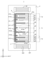
- FIG. 1 is a plan view of an elastic wave resonator according to an embodiment of the present invention.
- FIG. 1 is a plan view of an elastic wave resonator according to an embodiment of the present invention.
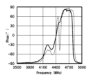
- FIG. 3 is a diagram showing resonance characteristics of an elastic wave resonator according to an embodiment of the present invention.
- FIG. 7 is another diagram showing the resonance characteristics of the elastic wave resonator according to one embodiment of the present invention.
- FIG. 7 is yet another diagram showing the resonance characteristics of the elastic wave resonator according to one embodiment of the present invention.
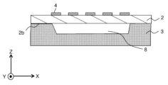
- FIG. 1 is a schematic cross-sectional view of an elastic wave resonator according to an embodiment of the present invention.
- FIG. 1 is a plan view of an elastic wave resonator according to an embodiment of the present invention.
- FIG. 3 is a diagram showing resonance characteristics of an elastic wave resonator according to an embodiment of
- FIG. 3 is a diagram showing the pitch difference required to represent a frequency difference of 50 MHz in a resonator with an anti-resonance frequency of 4600 MHz to 4950 MHz.
- FIG. 3 is a schematic cross-sectional view of an elastic wave resonator according to another embodiment of the present invention.
- FIG. 7 is a schematic cross-sectional view of an elastic wave resonator according to yet another embodiment of the present invention.
- 1 is a diagram schematically showing an elastic wave filter as a usage example of an elastic wave resonator according to an embodiment of the present invention.
- 1 is a block diagram showing the configuration of a main part of a communication device as an example of using an elastic wave resonator according to an embodiment of the present invention.
- an orthogonal coordinate system consisting of an X-axis, a Y-axis, and a Z-axis may be attached to the drawings.
- either direction may be upward or downward.
- the term upper surface or lower surface may be used with the Z-axis direction as the vertical direction.
- the X-axis is defined to be parallel to the propagation direction of SAW (Surface Acoustic Wave) that propagates along the upper surface of the piezoelectric layer 2, which will be described later, and the Y-axis is parallel to the upper surface of the piezoelectric layer 2 and It is defined to be perpendicular to the X-axis, and the Z-axis is defined to be perpendicular to the top surface of the piezoelectric layer 2.
- SAW Surface Acoustic Wave
- FIG. 1 is a schematic cross-sectional view of an elastic wave resonator 1 according to an embodiment of the present invention.
- an elastic wave resonator 1 includes a piezoelectric layer 2, a support substrate 3, and an IDT electrode 4.
- the support substrate 3 and the piezoelectric layer 2 are laminated in this order.
- the support substrate 3 supports the piezoelectric layer 2 laminated thereon, and the material of the support substrate 3 is not particularly limited as long as it has a certain strength.
- the support substrate 3 is made of a material with a smaller coefficient of linear expansion than the piezoelectric layer 2, it is possible to reduce the deformation of the piezoelectric layer 2 due to temperature changes, thereby changing the resonance characteristics due to temperature changes. can be reduced.
- the material of the support substrate 3 may be a material in which the transverse wave sound velocity of the elastic wave propagating is higher than the transverse wave sound velocity of the elastic wave propagating through the piezoelectric layer 2 .
- the elastic waves can be confined in the piezoelectric layer 2. Therefore, it is possible to provide an elastic wave resonator 1 with excellent frequency characteristics.
- Such materials include sapphire (Al 2 O 3 ) and silicon (Si).
- Si silicon
- a case where Si is used as the support substrate 3 will be explained as an example.
- the thickness of the support substrate 3 is not particularly limited, but is, for example, thicker than the thickness of the piezoelectric layer 2 described below.
- the piezoelectric layer 2 has an upper surface 2a and a lower surface 2b that are perpendicular to the Z-axis, with the Z-axis being the vertical direction.
- the aforementioned support substrate 3 is located on the lower surface 2b side.
- the lower surface 2b and the support substrate 3 may be in direct contact with each other, or may be in indirect contact with each other via, for example, an intermediate layer and a multilayer film layer 5, which will be described later. Further, the lower surface 2b and the support substrate 3 may be in indirect contact with each other via an adhesive layer (not shown) or the like.
- An IDT electrode 4, which will be described later, is located on the upper surface 2a side.
- the piezoelectric layer 2 includes, for example, a piezoelectric single-crystal substrate made of lithium tantalate (LiTaO 3 ; hereinafter referred to as LT) crystal and a piezoelectric substrate made of lithium niobate (LiNbO 3 ; hereinafter referred to as LN) crystal.
- LT lithium tantalate
- LN lithium niobate
- a single-crystal substrate having the same structure can be used.
- the piezoelectric layer 2 is constituted by a 120° Y cut-X propagation LN.
- an elastic wave propagating through the piezoelectric layer 2 in the propagation direction of the elastic wave is excited.
- the propagation direction is arbitrary, and may be, for example, a direction along the upper and lower surfaces of the piezoelectric layer 2 and/or a direction along the thickness of the piezoelectric layer 2.
- the elastic waves excited include plate waves or bulk waves.
- the elastic wave resonator 1 may use a plate wave or a bulk wave as a main mode.
- the plate wave may be a Lamb wave.
- the bulk wave may be an SH wave or a thickness-shear wave.
- the propagation mode of the plate wave to be used is not particularly limited. Specifically, in this embodiment, the plate wave is the A1 mode of the Lamb wave.
- the Lamb wave mainly includes a component (P component) in the arrangement direction (propagation direction) of the electrode fingers 412 and/or a component (SV component) in the thickness direction of the piezoelectric layer 2.
- the A1 mode refers to a first-order mode (one having one node in the thickness direction) among the asymmetric modes (A mode).
- the SH wave mainly has a component (SH component) in a direction perpendicular to the arrangement direction (propagation direction) of the electrode fingers 412 and horizontal to the surface of the piezoelectric layer 2.
- the thickness shear wave causes different parts (for example, the upper surface and lower surface) of the piezoelectric layer 2 in the thickness direction to slide in a direction along the upper surface and the lower surface of the piezoelectric layer 2, and also propagates in the thickness direction of the piezoelectric layer 2.
- the order of the thickness shear wave is arbitrary, for example, first order (the number of nodes in the thickness direction is one).
- the thickness of the piezoelectric layer 2 may be set as appropriate as long as it allows the use of plate waves.
- the thickness of the piezoelectric layer 2 is 2 ⁇ or less when expressed using ⁇ , which will be described later.
- the IDT electrode 4 is located on the upper surface 2a of the piezoelectric layer 2.
- the IDT electrode 4 is made of a conductive material.
- the IDT electrode 4 can be made of various conductive materials such as Al, Cu, Pt, Mo, Au, or an alloy thereof, and may also be constructed by laminating a plurality of these layers. .
- a base layer (not shown) may be interposed at the interface between the stacks.
- the IDT electrode 4 is made of Al.
- FIG. 2 schematically shows the shape of the IDT electrode 4 when viewed in plan from the Z-axis direction.
- the IDT electrode 4 includes a pair of comb-shaped electrodes 41.
- FIG. 2 schematically shows the shape of the IDT electrode 4 when viewed in plan from the Z-axis direction.
- the IDT electrode 4 includes a pair of comb-shaped electrodes 41.
- FIG. 2 schematically shows the shape of the IDT electrode 4 when viewed in plan from the Z-axis direction.
- the IDT electrode 4 includes a pair of comb-shaped electrodes 41.
- the comb-shaped electrodes 41 include, for example, a busbar 411 (411a and 411b) and a plurality of electrode fingers 412 (412a and 412b) mutually extending from the busbar 411, and are connected to one busbar 411a.
- the electrode finger 412a and the electrode finger 412b connected to the other bus bar 411b are arranged so as to mesh with each other.
- the comb-shaped electrode 41 protrudes from one bus bar 411 between each of the plurality of electrode fingers 412 and faces the electrode finger 412 extending from the other bus bar 411. ) may be included.
- the length of the plurality of electrode fingers 412 in the Y-axis direction may be set as appropriate depending on the required electrical characteristics and the like. For example, the lengths of the plurality of electrode fingers 412 in the Y-axis direction are equal to each other. Note that the IDT electrode 4 may be subjected to so-called apodization, in which the length of the plurality of electrode fingers 412 in the Y-axis direction (from another viewpoint, the intersection width) changes depending on the position in the propagation direction.
- the elastic wave resonator 1 may further include a pair of reflectors 42 on the top surface of the piezoelectric layer 2.
- the pair of reflectors 42 are located on both sides of the IDT electrode 4 in the propagation direction of the elastic wave.
- the reflector 42 includes a pair of reflector bus bars 421 facing each other and a plurality of strip electrodes 422 extending between the pair of reflector bus bars 421.
- the thickness of the plurality of electrode fingers 412 in the Z-axis direction may be set as appropriate depending on the required electrical characteristics and the like.
- the thickness of the plurality of electrode fingers 412 in the Z-axis direction may be constant.
- the width of one electrode finger 412a in the X-axis direction is defined as the width (w) of the electrode finger 412a.
- the distance from one side of the electrode finger 412a to one side of the electrode finger 412b adjacent to the electrode finger 412a is defined as the pitch (p) of the electrode finger 412a.
- the duty d of the electrode finger 412a represents the ratio of the width to the pitch of the electrode finger 412a. In other words, the duty d of the electrode fingers 412a can be expressed as width/pitch (w/p).
- Each of the plurality of electrode fingers 412 is arranged at intervals based on a predetermined pitch. Further, among the elastic waves propagating through the piezoelectric layer 2 , the resonance frequency of the elastic waves excited by the elastic wave resonator 1 depends on the pitch of the electrode fingers 412 .
- the plurality of electrode fingers 412 of the IDT electrode 4 are entirely located within the electrode finger arrangement region 7 in plan view.
- the electrode finger arrangement area 7 is an area where all of the plurality of electrode fingers 412 are located in plan view.
- the electrode finger arrangement region 7 is shown by dotted lines for convenience.
- the electrode finger arrangement region 7 includes at least one first region 71.
- the pitches of all the electrode fingers 412 located in the first region 71 are different from each other. Specifically, in FIG. 2, the pitches P1 to P6 of all the electrode fingers located in the first region 71 are different from each other. In this way, since the pitches of the electrode fingers 412 are different from each other, resonance of various unnecessary waves including second harmonic waves, third harmonic waves, etc. can be reduced, and the occurrence of spurious waves can be reduced.
- ⁇ is defined as twice the largest pitch among the pitches of the plurality of electrode fingers located in the first region.
- ⁇ is often used as a symbol representing wavelength.
- the wavelength of the plate wave may or may not be the same size as ⁇ .
- the wavelength of the Lamb wave in A1 mode tends to be relatively close to ⁇ .
- the wavelength of the thickness shear wave has a dependence on ⁇ , but the dependence on the thickness of the piezoelectric layer 2 is relatively large and is not necessarily close to ⁇ .
- the electrode finger arrangement region 7 may include a second region 72. All the electrode fingers 412 located in the second region 72 have the same pitch.
- the pitch is constant does not necessarily mean that it is strictly constant, but allows for some variation within a range that can be called manufacturing error.
- the range that can be called a manufacturing error is, for example, a range of 1.5% or less with respect to the average value of the pitch of the electrode fingers 412 located in that region.
- the pitch can be kept constant. If it is clear that the pitch is not intended to be constant, it is not necessary to consider the above-mentioned adjacent pitches to be constant.
- the electrode finger 412 located at the boundary between the first region 71 and the second region 72 may be interpreted as being included in both the first region and the second region. Electrode fingers 412 located at the boundary between the center region and regions on both sides thereof, which will be described later, may be similarly interpreted as being included in the center region.
- the elastic wave resonator 1 of this embodiment uses plate waves as a main mode.
- the resonance characteristics of the plate wave largely depend on the thickness of the piezoelectric layer 2.
- the resonance of the plate wave is not easily affected by the difference in the pitch of the electrode fingers 412. Therefore, in this embodiment, since the elastic wave resonator 1 uses plate waves and the pitches of all the electrode fingers 412 located in the first region 71 are different from each other, the resonance of the main mode due to the plate waves can be achieved relatively well. It is possible to effectively reduce the resonance of spurious modes caused by unnecessary waves while maintaining the Note that using a plate wave as the main mode means that the main mode of the elastic wave excited by the IDT electrode 4 is a plate wave.
- the first region 71 may occupy half or more of the area of the electrode finger arrangement region 7.
- the regions in which the electrode fingers 412 have different pitches become dominant, and it is possible to more effectively reduce the occurrence of spurious signals with large phases.
- the vicinity of the center of the electrode finger arrangement region 7 in the arrangement direction of the electrode fingers 412 may belong to the first region 71.
- the vicinity of the center refers to, for example, a region on the center side when the electrode finger arrangement region 7 is divided into three equal parts in the arrangement direction of the electrode fingers 412.
- the entire electrode finger arrangement region 7 may belong to the first region 71.
- the area occupied by the area in which the generation of spurious waves is reduced becomes larger, and the generation of spurious waves can be reduced more effectively.
- FIGS. 4A to 4C show diagrams comparing the resonance characteristics of the elastic wave resonator 1 according to an example of the present invention and the resonance characteristics of an elastic wave resonator according to a comparative example.
- FIG. 4A is a diagram showing the entire resonance characteristic
- FIG. 4B is an enlarged diagram of the resonance due to the main mode
- FIG. 4C is a diagram showing the resonance due to the spurious mode enlarged.
- the solid line shows the characteristics of the example
- the dotted line shows the characteristics of the comparative example.
- the designs of the elastic wave resonator 1 according to an embodiment of the present invention and the elastic wave resonator according to a comparative example are as follows.
- Comparative example piezoelectric layer: LN, IDT electrode: Al, pitch: 2.18 ⁇ m, duty d: 0.3)
- the pitch of 2.12 ⁇ m to 2.42 ⁇ m means that the pitch increases continuously in one direction from 2.12 ⁇ m to 2.42 ⁇ m.
- the entire electrode finger arrangement region 7 belongs to the first region 71 in the embodiment.
- the elastic wave resonator 1 according to the embodiment of the present invention has reduced resonance due to spurious modes compared to the elastic wave resonator according to the comparative example.
- the main mode resonance has a smaller loss than the spurious mode, and still maintains good characteristics.
- the pitch of the plurality of electrode fingers 412 located in the first region 71 is not particularly limited as long as the pitches are different from each other.
- the pitches of the plurality of electrode fingers 412 located in the first region 71 may increase by the same amount or rate of increase toward the first direction (the direction in which the electrode fingers 412 are arranged).
- FIG. 5 is a diagram showing the pitch difference necessary to express a frequency difference of 50 MHz in a resonator with an anti-resonance frequency of 4600 MHz to 4950 MHz.
- the vertical axis represents the value of 100 ⁇ (Pmax-Pmin)/Pmax, where Pmax is the largest pitch among the pitches of the plurality of electrode fingers 412 located in the first region 71, and Pmin is the smallest pitch. It shows.
- the horizontal axis indicates the value of the duty d of the electrode finger 412 located in the first region 71.
- each plot represents the change in the thickness of LN in the range of 0.47 ⁇ m to 0.5 ⁇ m.
- the pitch of the plurality of electrode fingers 412 located in the first region 71 may be 100 ⁇ (Pmax ⁇ Pmin)/Pmax ⁇ 3.0.
- the difference between the maximum pitch and the minimum pitch of the plurality of electrode fingers 412 located in the first region 71 is 50 MHz or more, so that the resonance waveform due to the spurious mode is more effectively broadened. be able to. Thereby, for example, the influence on the pass characteristics of the filter can be reduced.
- the piezoelectric layer 2 is constituted by a 120° Y cut-X propagation LN, but the present invention is not limited to this example.
- the Euler angle of the piezoelectric layer 2 may be set as appropriate.
- the Euler angle of the piezoelectric layer 2 may be (0°, ⁇ + ( ⁇ ⁇ 180), 0°) ( ⁇ is any value in the range of 0° to 180°, and ⁇ is an integer from 0 to 2. ).
- the piezoelectric layer 2 may be formed of a Z-cut LN or LT. In this case, for example, thickness-shear waves can be effectively utilized.
- the thickness of the piezoelectric layer 2 that overlaps with the first region 71 may be constant in plan view. With such a configuration, it is possible to reduce the resonance loss of the plate wave used, and provide the elastic wave resonator 1 having good filter characteristics. Note that the term "the thickness of the piezoelectric layer 2 is constant" does not necessarily mean that it is strictly constant, but rather that it may vary slightly within a range that does not significantly affect the characteristics of the elastic waves propagating through the piezoelectric layer 2. Allow.
- the support substrate 3 has the configuration shown in FIG. 1, but is not limited to this example.
- the support substrate 3 may have a void 8 on the top surface.
- the piezoelectric layer 2 covers the gap 8 of the support substrate 3, leaving a space inside the gap 8 in a plan view. Note that the size and depth of the void 8 may be set as appropriate.
- the piezoelectric layer 2 and the support substrate 3 are in direct contact with each other, but the present invention is not limited to this example.
- the lower surface 2b of the piezoelectric layer 2 and the support substrate 3 may be in direct contact with each other, or may be in indirect contact with each other via, for example, an intermediate layer and an adhesive layer (not shown).
- Examples of such an intermediate layer include insulating materials such as silicon oxide (SiO 2 ), silicon nitride (Si 3 N 4 ), and aluminum oxide (Al 2 O 3 ). By providing such an insulating intermediate layer, it is possible to reduce the formation of unnecessary potential and unnecessary capacitance, and it is possible to improve the electrical characteristics of the acoustic wave resonator 1. .
- both an adhesive layer and an intermediate layer may be located between the piezoelectric layer 2 and the support substrate 3.
- the adhesive layer is located between the support substrate 3 and the intermediate layer.
- An example of such an adhesive layer is amorphous silicon.
- an alumina film (not shown) or the like may be further located between the intermediate layer and the piezoelectric layer 2.
- an alumina film (not shown) or the like may be further located between the intermediate layer and the piezoelectric layer 2.
- an alumina film it is possible to reduce the leakage of elastic waves from the piezoelectric layer 2 to the support substrate 3 side, and it is possible to improve the frequency characteristics of the elastic wave resonator 1.
- FIG. 6B shows a schematic cross-sectional view of an elastic wave resonator 1 according to yet another embodiment.
- a multilayer film layer 5 may be located between the piezoelectric layer 2 and the support substrate 3.
- low acoustic impedance layers 51 and high acoustic impedance layers 52 are alternately laminated.
- the acoustic impedance of the low acoustic impedance layer 51 is lower than that of the piezoelectric layer 2
- the acoustic impedance of the high acoustic impedance layer 52 is higher than that of the low acoustic impedance layer 51 .
- the low acoustic impedance layer 51 is silicon oxide (SiO 2 )
- the high acoustic impedance layer 52 is hafnium oxide (HfO 2 ).
- the duty d of the electrode fingers 412 located in the first region 71 may be constant. Since the pitches of the electrode fingers 412 located in the first region 71 are different from each other, when the value of the duty d of the electrode fingers 412 located in the first region 71 is constant, the expected value is lower than when the duty d is different. It is possible to reduce the possibility that spurious will occur due to resonance that was not present, and to effectively reduce spurious.
- the value of the duty d of the electrode finger 412 located in the first region 71 is 0.6 or less. Note that the constant value of the duty d does not necessarily mean that it is strictly constant, but allows for some variation within a range of, for example, 0.01 or less.
- the thickness of the electrode fingers 412 located in the first region 71 may be constant, or may be set to a different thickness for each electrode finger 412 as appropriate. good.
- the first region 71 may occupy half or more of the area of the electrode finger arrangement region 7, but the present invention is not limited to this example.
- the number of electrode fingers 412 located in the first region 71 may be half or more of the total number of the plurality of electrode fingers 412 located in the electrode finger arrangement region 7.
- the specific value of the number of electrode fingers 412 located in the first region 71 is not particularly limited. Theoretically, the number is 3 or more, which constitutes a pitch of 2 or more, and in practice, for example, it is 5 or more, 10 or more, 30 or more, 50 or more, or 100 or more. good.
- the pitches of all the electrode fingers 412 in the first region 71 may be different from each other, but the pitch is not limited to this example.
- the pitch of the electrode fingers 412 may increase toward one side in the first direction (the direction in which the electrode fingers 412 are arranged).
- the central region may include a portion where the pitch is constant.
- the pitch may not increase continuously in a part or all of the central region, but may increase stepwise (stepwise). Even in this case, effects such as broadening can still be obtained.
- the number of pitch changes in the central region is not particularly limited. Theoretically, the number of changes is 1 or more, and in practice, it may be, for example, 5 or more, 10 or more, 30 or more, 50 or more, or 100 or more.
- FIG. 7 is a circuit diagram schematically showing the configuration of an elastic wave filter 101 as an example of how the elastic wave resonator 1 is used.
- the comb-shaped electrode 41 is schematically shown in the form of a forked fork in this drawing, and the reflector 42 is a single piece with bent ends. It is represented by a line.
- the elastic wave filter 101 filters a signal input from the input terminal 102 and outputs the filtered signal to the output terminal 103.
- the elastic wave filter 101 is configured by, for example, a ladder type filter in which a plurality of resonators are connected in a ladder type. That is, the elastic wave filter 101 includes a plurality of resonators (series resonators) connected in series between an input terminal 102 and an output terminal 103, and a line in series with the reference potential. It has a plurality of (or even one) resonators (parallel resonators) to be connected.
- At least one of the resonators included in the elastic wave filter 101 in this embodiment is the elastic wave resonator 1 in this embodiment.
- a resonator made up of the elastic wave resonator 1 will be referred to as a first elastic wave resonator 11.
- the elastic wave filter 101 includes a second elastic wave resonator 12.
- the anti-resonant frequency of the second elastic wave resonator 12 is lower than the anti-resonant frequency of the first elastic wave resonator 11. may also be located near the passband of the elastic wave filter 101.
- the elastic wave filter 101 may be designed so that (P2max-P2min) is smaller than (P1max-P1min).
- the second elastic wave resonator 12 has a smaller pitch difference than the first elastic wave resonator 11.
- a resonator with a small pitch difference has less main mode resonance loss than a resonator with a large pitch difference. Therefore, between the anti-resonant frequency of the first elastic wave resonator 11 and the passband of the elastic wave filter 101, the anti-resonant frequency of the second elastic wave resonator 12, which has a pitch difference smaller than that of the first elastic wave resonator 11, is generated.
- the main mode of the resonator near the passband of the filter, the loss of the main mode of the resonator can be reduced. Therefore, it is possible to provide an elastic wave filter with highly steep filter characteristics.
- the resonant frequency of the second elastic wave resonator 12 is more elastic than the resonant frequency of the first elastic wave resonator 11. It may be located near the passband of wave filter 101.
- the elastic wave filter 101 may be designed so that (P2max-P2min) is smaller than (P1max-P1min).
- the second elastic wave resonator 12 has a smaller pitch difference than the first elastic wave resonator 11. Therefore, between the anti-resonant frequency of the first elastic wave resonator 11 and the passband of the elastic wave filter 101, the anti-resonant frequency of the second elastic wave resonator 12, which has a pitch difference smaller than that of the first elastic wave resonator 11, is generated.
- the main mode of the resonator near the passband of the filter, the loss of the main mode of the resonator can be reduced. Therefore, it is possible to provide an elastic wave filter with highly steep filter characteristics.
- the maximum phase of the spurious generated from the first elastic wave resonator 11 that exists in the pass band of the elastic wave filter 101 may be -70° or less. good.
- the maximum phase of the spurious generated from the first elastic wave resonator 11 that exists in the passband of the elastic wave filter 101 may be located in the range of ⁇ 80° to ⁇ 70°.
- a spurious signal with a small phase is located in the passband of the elastic wave filter 101, and the influence of the spurious signal on the filter can be reduced.
- the elastic wave filter 101 is a ladder type filter, it is not limited to this example.
- the elastic wave filter 101 may be a multimode filter (including a double mode filter).
- the multimode filter includes a plurality of IDT electrodes 4 arranged in the propagation direction of elastic waves and a pair of reflectors 42 arranged on both sides of the IDT electrodes 4.
- FIG. 8 is a block diagram showing main parts of a communication device 111 as an example of using the elastic wave resonator 1 and the elastic wave filter 101.
- the communication device 111 performs wireless communication using radio waves, and includes a duplexer 116.
- the duplexer 116 includes a transmission filter 101a and a reception filter 101b. At least one of the transmission filter 101a and the reception filter 101b is configured by an elastic wave filter 101. Both the output side of the transmission filter 101a and the input side of the reception filter 101b are connected to an antenna 112.
- a transmission information signal TIS containing information to be transmitted is modulated and frequency-increased (conversion of carrier frequency to a high-frequency signal) by an RF-IC (Radio Frequency Integrated Circuit) 113, and is converted into a transmission signal TS.
- the transmission signal TS has unnecessary components outside the transmission passband removed by the bandpass filter 115a, is amplified by the amplifier 114a, and is input to the duplexer 116 (transmission filter 101a). Then, the duplexer 116 (transmission filter 101a) removes unnecessary components outside the transmission passband from the input transmission signal TS, and outputs the removed transmission signal TS to the antenna 112.
- the antenna 112 converts the input electrical signal (transmission signal TS) into a wireless signal (radio wave) and transmits the signal.
- a wireless signal (radio wave) received by the antenna 112 is converted into an electric signal (received signal RS) by the antenna 112 and input to the duplexer 116 .
- the duplexer 116 (reception filter 101b) removes unnecessary components outside the reception passband from the input reception signal RS, and outputs the removed signal to the amplifier 114b.
- the output received signal RS is amplified by the amplifier 114b, and unnecessary components outside the receiving passband are removed by the bandpass filter 115b. Then, the received signal RS is lowered in frequency and demodulated by the RF-IC 113 to become a received information signal RIS.
- the transmission information signal TIS and the reception information signal RIS may be low frequency signals (baseband signals) containing appropriate information, such as analog audio signals or digitized audio signals.
- the passband of the wireless signal may be set as appropriate, and in this embodiment, a relatively high frequency passband (for example, 5 GHz or higher) is also possible.
- the modulation method may be phase modulation, amplitude modulation, frequency modulation, or a combination of two or more of these.
- the direct conversion system is illustrated as an example of the circuit system in FIG. 8, it may be any other suitable circuit system, for example, a double superheterodyne system. Further, FIG. 8 schematically shows only the main parts, and a low-pass filter or isolator or the like may be added at an appropriate position, or the position of an amplifier or the like may be changed.
Landscapes
- Physics & Mathematics (AREA)
- Acoustics & Sound (AREA)
- Surface Acoustic Wave Elements And Circuit Networks Thereof (AREA)
Priority Applications (1)
| Application Number | Priority Date | Filing Date | Title |
|---|---|---|---|
| JP2024537743A JP7793060B2 (ja) | 2022-07-29 | 2023-07-25 | 弾性波共振子、弾性波フィルタおよび通信装置 |
Applications Claiming Priority (2)
| Application Number | Priority Date | Filing Date | Title |
|---|---|---|---|
| JP2022-121813 | 2022-07-29 | ||
| JP2022121813 | 2022-07-29 |
Publications (1)
| Publication Number | Publication Date |
|---|---|
| WO2024024778A1 true WO2024024778A1 (ja) | 2024-02-01 |
Family
ID=89706411
Family Applications (1)
| Application Number | Title | Priority Date | Filing Date |
|---|---|---|---|
| PCT/JP2023/027168 Ceased WO2024024778A1 (ja) | 2022-07-29 | 2023-07-25 | 弾性波共振子、弾性波フィルタおよび通信装置 |
Country Status (2)
| Country | Link |
|---|---|
| JP (1) | JP7793060B2 (https=) |
| WO (1) | WO2024024778A1 (https=) |
Cited By (2)
| Publication number | Priority date | Publication date | Assignee | Title |
|---|---|---|---|---|
| CN118353414A (zh) * | 2024-06-17 | 2024-07-16 | 天通瑞宏科技有限公司 | 一种声表面波谐振器及声表面波滤波器 |
| WO2025263150A1 (ja) * | 2024-06-20 | 2025-12-26 | 株式会社村田製作所 | 弾性波装置 |
Citations (6)
| Publication number | Priority date | Publication date | Assignee | Title |
|---|---|---|---|---|
| JPH09261001A (ja) * | 1996-03-25 | 1997-10-03 | Mitsui Mining & Smelting Co Ltd | 弾性表面波変換器 |
| JP2005176254A (ja) * | 2003-12-15 | 2005-06-30 | Kyocera Corp | 弾性表面波装置および通信装置 |
| WO2019117133A1 (ja) * | 2017-12-12 | 2019-06-20 | 株式会社村田製作所 | マルチプレクサ、高周波フロントエンド回路および通信装置 |
| JP2021100280A (ja) * | 2018-11-14 | 2021-07-01 | 京セラ株式会社 | 弾性波装置、分波器および通信装置 |
| WO2021177108A1 (ja) * | 2020-03-06 | 2021-09-10 | 京セラ株式会社 | 弾性波共振子、弾性波フィルタ、分波器、通信装置 |
| WO2022085581A1 (ja) * | 2020-10-23 | 2022-04-28 | 株式会社村田製作所 | 弾性波装置 |
-
2023
- 2023-07-25 JP JP2024537743A patent/JP7793060B2/ja active Active
- 2023-07-25 WO PCT/JP2023/027168 patent/WO2024024778A1/ja not_active Ceased
Patent Citations (6)
| Publication number | Priority date | Publication date | Assignee | Title |
|---|---|---|---|---|
| JPH09261001A (ja) * | 1996-03-25 | 1997-10-03 | Mitsui Mining & Smelting Co Ltd | 弾性表面波変換器 |
| JP2005176254A (ja) * | 2003-12-15 | 2005-06-30 | Kyocera Corp | 弾性表面波装置および通信装置 |
| WO2019117133A1 (ja) * | 2017-12-12 | 2019-06-20 | 株式会社村田製作所 | マルチプレクサ、高周波フロントエンド回路および通信装置 |
| JP2021100280A (ja) * | 2018-11-14 | 2021-07-01 | 京セラ株式会社 | 弾性波装置、分波器および通信装置 |
| WO2021177108A1 (ja) * | 2020-03-06 | 2021-09-10 | 京セラ株式会社 | 弾性波共振子、弾性波フィルタ、分波器、通信装置 |
| WO2022085581A1 (ja) * | 2020-10-23 | 2022-04-28 | 株式会社村田製作所 | 弾性波装置 |
Cited By (2)
| Publication number | Priority date | Publication date | Assignee | Title |
|---|---|---|---|---|
| CN118353414A (zh) * | 2024-06-17 | 2024-07-16 | 天通瑞宏科技有限公司 | 一种声表面波谐振器及声表面波滤波器 |
| WO2025263150A1 (ja) * | 2024-06-20 | 2025-12-26 | 株式会社村田製作所 | 弾性波装置 |
Also Published As
| Publication number | Publication date |
|---|---|
| JP7793060B2 (ja) | 2025-12-26 |
| JPWO2024024778A1 (https=) | 2024-02-01 |
Similar Documents
| Publication | Publication Date | Title |
|---|---|---|
| CN101796727B (zh) | 弹性边界波装置 | |
| JP7278305B2 (ja) | 弾性波装置、分波器および通信装置 | |
| JP6530494B2 (ja) | 弾性表面波素子 | |
| JP6760480B2 (ja) | エクストラクタ | |
| JP6870684B2 (ja) | マルチプレクサ | |
| US10193529B2 (en) | Elastic wave device | |
| US11569433B2 (en) | Acoustic wave resonator, filter, and multiplexer | |
| CN109845105B (zh) | 弹性波滤波器装置 | |
| CN111937305A (zh) | 弹性波元件、弹性波滤波器、分波器以及通信装置 | |
| JP7793060B2 (ja) | 弾性波共振子、弾性波フィルタおよび通信装置 | |
| CN114270707A (zh) | 弹性波装置 | |
| JP7117880B2 (ja) | 弾性波フィルタ、分波器および通信装置 | |
| JP7386741B2 (ja) | フィルタ、分波器及び通信装置 | |
| JP2018137517A (ja) | 弾性表面波共振子、分波器および通信装置 | |
| JP7416080B2 (ja) | 弾性波装置、フィルタ装置及びマルチプレクサ | |
| JP2026008701A (ja) | 弾性波装置、通信装置、圧電基板 | |
| US20250105822A1 (en) | Filter device, splitter, and communication device | |
| WO2024128020A1 (ja) | 弾性波共振子、フィルタデバイスおよび通信装置 | |
| JP2025003073A (ja) | フィルタデバイスおよび通信装置 | |
| WO2023033032A1 (ja) | 弾性波素子、分波器および通信装置 | |
| WO2024190677A1 (ja) | 弾性波共振子および通信装置 | |
| WO2024225181A1 (ja) | 弾性波共振子および通信装置 | |
| JP2025179286A (ja) | 弾性波共振子および通信装置 | |
| WO2024190719A1 (ja) | 弾性波デバイスおよび通信装置 | |
| WO2023171715A1 (ja) | 弾性波装置、分波器、通信装置および弾性波装置の製造方法 |
Legal Events
| Date | Code | Title | Description |
|---|---|---|---|
| 121 | Ep: the epo has been informed by wipo that ep was designated in this application |
Ref document number: 23846508 Country of ref document: EP Kind code of ref document: A1 |
|
| WWE | Wipo information: entry into national phase |
Ref document number: 2024537743 Country of ref document: JP |
|
| NENP | Non-entry into the national phase |
Ref country code: DE |
|
| 122 | Ep: pct application non-entry in european phase |
Ref document number: 23846508 Country of ref document: EP Kind code of ref document: A1 |