WO2024024778A1 - Elastic wave resonator, elastic wave filter, and communication device - Google Patents
Elastic wave resonator, elastic wave filter, and communication device Download PDFInfo
- Publication number
- WO2024024778A1 WO2024024778A1 PCT/JP2023/027168 JP2023027168W WO2024024778A1 WO 2024024778 A1 WO2024024778 A1 WO 2024024778A1 JP 2023027168 W JP2023027168 W JP 2023027168W WO 2024024778 A1 WO2024024778 A1 WO 2024024778A1
- Authority
- WO
- WIPO (PCT)
- Prior art keywords
- elastic wave
- wave resonator
- electrode
- region
- pitch
- Prior art date
Links
- 239000011295 pitch Substances 0.000 claims abstract description 106
- 230000001902 propagating effect Effects 0.000 claims description 9
- 235000019687 Lamb Nutrition 0.000 claims description 6
- 239000010410 layer Substances 0.000 description 78
- 239000000758 substrate Substances 0.000 description 27
- 230000005540 biological transmission Effects 0.000 description 14
- 238000010586 diagram Methods 0.000 description 13
- 239000000463 material Substances 0.000 description 7
- 239000012790 adhesive layer Substances 0.000 description 6
- 230000000052 comparative effect Effects 0.000 description 5
- 239000013078 crystal Substances 0.000 description 4
- 238000010897 surface acoustic wave method Methods 0.000 description 3
- 229910004298 SiO 2 Inorganic materials 0.000 description 2
- VYPSYNLAJGMNEJ-UHFFFAOYSA-N Silicium dioxide Chemical compound O=[Si]=O VYPSYNLAJGMNEJ-UHFFFAOYSA-N 0.000 description 2
- PNEYBMLMFCGWSK-UHFFFAOYSA-N aluminium oxide Inorganic materials [O-2].[O-2].[O-2].[Al+3].[Al+3] PNEYBMLMFCGWSK-UHFFFAOYSA-N 0.000 description 2
- 238000006243 chemical reaction Methods 0.000 description 2
- 239000004020 conductor Substances 0.000 description 2
- 238000004519 manufacturing process Methods 0.000 description 2
- TWNQGVIAIRXVLR-UHFFFAOYSA-N oxo(oxoalumanyloxy)alumane Chemical compound O=[Al]O[Al]=O TWNQGVIAIRXVLR-UHFFFAOYSA-N 0.000 description 2
- 229910052814 silicon oxide Inorganic materials 0.000 description 2
- 230000005236 sound signal Effects 0.000 description 2
- 239000011800 void material Substances 0.000 description 2
- WSMQKESQZFQMFW-UHFFFAOYSA-N 5-methyl-pyrazole-3-carboxylic acid Chemical compound CC1=CC(C(O)=O)=NN1 WSMQKESQZFQMFW-UHFFFAOYSA-N 0.000 description 1
- 229910018072 Al 2 O 3 Inorganic materials 0.000 description 1
- 229910013641 LiNbO 3 Inorganic materials 0.000 description 1
- 229910052581 Si3N4 Inorganic materials 0.000 description 1
- XUIMIQQOPSSXEZ-UHFFFAOYSA-N Silicon Chemical compound [Si] XUIMIQQOPSSXEZ-UHFFFAOYSA-N 0.000 description 1
- 239000000956 alloy Substances 0.000 description 1
- 229910045601 alloy Inorganic materials 0.000 description 1
- 229910052782 aluminium Inorganic materials 0.000 description 1
- 229910021417 amorphous silicon Inorganic materials 0.000 description 1
- 230000015572 biosynthetic process Effects 0.000 description 1
- 229910052802 copper Inorganic materials 0.000 description 1
- 230000000694 effects Effects 0.000 description 1
- 230000008030 elimination Effects 0.000 description 1
- 238000003379 elimination reaction Methods 0.000 description 1
- CJNBYAVZURUTKZ-UHFFFAOYSA-N hafnium(iv) oxide Chemical compound O=[Hf]=O CJNBYAVZURUTKZ-UHFFFAOYSA-N 0.000 description 1
- 239000011810 insulating material Substances 0.000 description 1
- 238000010030 laminating Methods 0.000 description 1
- GQYHUHYESMUTHG-UHFFFAOYSA-N lithium niobate Chemical compound [Li+].[O-][Nb](=O)=O GQYHUHYESMUTHG-UHFFFAOYSA-N 0.000 description 1
- 238000000034 method Methods 0.000 description 1
- 229910052697 platinum Inorganic materials 0.000 description 1
- 229910052710 silicon Inorganic materials 0.000 description 1
- 239000010703 silicon Substances 0.000 description 1
- HQVNEWCFYHHQES-UHFFFAOYSA-N silicon nitride Chemical compound N12[Si]34N5[Si]62N3[Si]51N64 HQVNEWCFYHHQES-UHFFFAOYSA-N 0.000 description 1
Images


Classifications
-
- H—ELECTRICITY
- H03—ELECTRONIC CIRCUITRY
- H03H—IMPEDANCE NETWORKS, e.g. RESONANT CIRCUITS; RESONATORS
- H03H9/00—Networks comprising electromechanical or electro-acoustic devices; Electromechanical resonators
- H03H9/02—Details
- H03H9/125—Driving means, e.g. electrodes, coils
- H03H9/145—Driving means, e.g. electrodes, coils for networks using surface acoustic waves
-
- H—ELECTRICITY
- H03—ELECTRONIC CIRCUITRY
- H03H—IMPEDANCE NETWORKS, e.g. RESONANT CIRCUITS; RESONATORS
- H03H9/00—Networks comprising electromechanical or electro-acoustic devices; Electromechanical resonators
- H03H9/46—Filters
- H03H9/64—Filters using surface acoustic waves
-
- H—ELECTRICITY
- H03—ELECTRONIC CIRCUITRY
- H03H—IMPEDANCE NETWORKS, e.g. RESONANT CIRCUITS; RESONATORS
- H03H9/00—Networks comprising electromechanical or electro-acoustic devices; Electromechanical resonators
- H03H9/70—Multiple-port networks for connecting several sources or loads, working on different frequencies or frequency bands, to a common load or source
- H03H9/72—Networks using surface acoustic waves
Definitions
- the present invention relates to an elastic wave resonator that is an electronic component that utilizes elastic waves, an elastic wave filter having the elastic wave resonator, and a communication device.
- An elastic wave resonator in which a voltage is applied to an IDT (interdigital transducer) electrode formed of a plurality of electrode fingers provided on the surface of a piezoelectric substrate to generate an elastic wave that propagates through a piezoelectric material.
- the IDT electrode has a gradation region in which the electrode finger pitch is gradually reduced at both ends.
- An elastic wave resonator includes a piezoelectric layer and an IDT electrode.
- the piezoelectric layer has piezoelectricity.
- the IDT electrode is located on the first surface of the piezoelectric layer and has a plurality of electrode fingers arranged in a first direction. All of the plurality of electrode fingers are located in the electrode finger arrangement region. The distance from one side of one electrode finger to the one side of the electrode finger adjacent to the one electrode finger in the first direction is defined as the pitch of the one electrode finger.
- the electrode finger arrangement region has a first region in which all the electrode fingers have different pitches.
- the elastic wave resonator is configured to use a plate wave or a bulk wave as an elastic wave propagating in the electrode finger arrangement region.
- An elastic wave resonator includes a piezoelectric layer and an IDT electrode.
- the piezoelectric layer has piezoelectricity.
- the IDT electrode is located on the first surface of the piezoelectric layer and has a plurality of electrode fingers arranged in a first direction. All of the plurality of electrode fingers are located in the electrode finger arrangement region. The distance from one side of one electrode finger to the one side of the electrode finger adjacent to the one electrode finger in the first direction is defined as the pitch of the one electrode finger. In the central region where the electrode finger arrangement region is divided into three equal parts in the first direction, the pitch of the electrode fingers increases toward the one side.
- An elastic wave filter is a ladder-type elastic wave filter including a plurality of series arm resonators connected in series and a parallel arm resonator connected in parallel to the series arm resonators. It's a filter.
- the plurality of series resonators include any of the elastic wave resonators described above and a second elastic wave resonator.
- the anti-resonant frequency of the second elastic wave resonator is located closer to the passband of the elastic wave filter than the anti-resonant frequency of the elastic wave resonator.
- the pitches of the plurality of electrode fingers of the IDT electrode of the elastic wave resonator the largest pitch is defined as P1max, and the smallest pitch is defined as P1min.
- the largest pitch is defined as P2max, and the smallest pitch is defined as P2min. (P2max-P2min) is smaller than (P1max-P1min).
- An elastic wave filter is a ladder-type elastic wave filter including a series arm resonator connected in series and a plurality of parallel arm resonators connected in parallel to the series arm resonator. It's a filter.
- the plurality of parallel arm resonators include any of the elastic wave resonators described above and a second elastic wave resonator.
- the resonant frequency of the second elastic wave resonator is located closer to the passband of the elastic wave filter than the resonant frequency of the elastic wave resonator.
- the pitches of the plurality of electrode fingers of the IDT electrode of the elastic wave resonator the largest pitch is defined as P1max, and the smallest pitch is defined as P1min.
- the largest pitch is defined as P2max, and the smallest pitch is defined as P2min. (P2max-P2min) is smaller than (P1max-P1min).
- An elastic wave filter according to an embodiment of the present invention is an elastic wave filter having an elastic wave resonator described in any one of the above, wherein the elastic wave resonator exists in a passband of the elastic wave filter.
- the maximum phase of the derived spurious is -70° or less.
- a communication device includes an antenna, an elastic wave filter connected to the antenna, and an IC connected to the elastic wave filter.
- the elastic wave filter includes the elastic wave resonator.
- FIG. 1 is a schematic cross-sectional view of an elastic wave resonator according to an embodiment of the present invention.
- FIG. 1 is a plan view of an elastic wave resonator according to an embodiment of the present invention.
- FIG. 1 is a plan view of an elastic wave resonator according to an embodiment of the present invention.
- FIG. 3 is a diagram showing resonance characteristics of an elastic wave resonator according to an embodiment of the present invention.
- FIG. 7 is another diagram showing the resonance characteristics of the elastic wave resonator according to one embodiment of the present invention.
- FIG. 7 is yet another diagram showing the resonance characteristics of the elastic wave resonator according to one embodiment of the present invention.
- FIG. 1 is a schematic cross-sectional view of an elastic wave resonator according to an embodiment of the present invention.
- FIG. 1 is a plan view of an elastic wave resonator according to an embodiment of the present invention.
- FIG. 3 is a diagram showing resonance characteristics of an elastic wave resonator according to an embodiment of
- FIG. 3 is a diagram showing the pitch difference required to represent a frequency difference of 50 MHz in a resonator with an anti-resonance frequency of 4600 MHz to 4950 MHz.
- FIG. 3 is a schematic cross-sectional view of an elastic wave resonator according to another embodiment of the present invention.
- FIG. 7 is a schematic cross-sectional view of an elastic wave resonator according to yet another embodiment of the present invention.
- 1 is a diagram schematically showing an elastic wave filter as a usage example of an elastic wave resonator according to an embodiment of the present invention.
- 1 is a block diagram showing the configuration of a main part of a communication device as an example of using an elastic wave resonator according to an embodiment of the present invention.
- an orthogonal coordinate system consisting of an X-axis, a Y-axis, and a Z-axis may be attached to the drawings.
- either direction may be upward or downward.
- the term upper surface or lower surface may be used with the Z-axis direction as the vertical direction.
- the X-axis is defined to be parallel to the propagation direction of SAW (Surface Acoustic Wave) that propagates along the upper surface of the piezoelectric layer 2, which will be described later, and the Y-axis is parallel to the upper surface of the piezoelectric layer 2 and It is defined to be perpendicular to the X-axis, and the Z-axis is defined to be perpendicular to the top surface of the piezoelectric layer 2.
- SAW Surface Acoustic Wave
- FIG. 1 is a schematic cross-sectional view of an elastic wave resonator 1 according to an embodiment of the present invention.
- an elastic wave resonator 1 includes a piezoelectric layer 2, a support substrate 3, and an IDT electrode 4.
- the support substrate 3 and the piezoelectric layer 2 are laminated in this order.
- the support substrate 3 supports the piezoelectric layer 2 laminated thereon, and the material of the support substrate 3 is not particularly limited as long as it has a certain strength.
- the support substrate 3 is made of a material with a smaller coefficient of linear expansion than the piezoelectric layer 2, it is possible to reduce the deformation of the piezoelectric layer 2 due to temperature changes, thereby changing the resonance characteristics due to temperature changes. can be reduced.
- the material of the support substrate 3 may be a material in which the transverse wave sound velocity of the elastic wave propagating is higher than the transverse wave sound velocity of the elastic wave propagating through the piezoelectric layer 2 .
- the elastic waves can be confined in the piezoelectric layer 2. Therefore, it is possible to provide an elastic wave resonator 1 with excellent frequency characteristics.
- Such materials include sapphire (Al 2 O 3 ) and silicon (Si).
- Si silicon
- a case where Si is used as the support substrate 3 will be explained as an example.
- the thickness of the support substrate 3 is not particularly limited, but is, for example, thicker than the thickness of the piezoelectric layer 2 described below.
- the piezoelectric layer 2 has an upper surface 2a and a lower surface 2b that are perpendicular to the Z-axis, with the Z-axis being the vertical direction.
- the aforementioned support substrate 3 is located on the lower surface 2b side.
- the lower surface 2b and the support substrate 3 may be in direct contact with each other, or may be in indirect contact with each other via, for example, an intermediate layer and a multilayer film layer 5, which will be described later. Further, the lower surface 2b and the support substrate 3 may be in indirect contact with each other via an adhesive layer (not shown) or the like.
- An IDT electrode 4, which will be described later, is located on the upper surface 2a side.
- the piezoelectric layer 2 includes, for example, a piezoelectric single-crystal substrate made of lithium tantalate (LiTaO 3 ; hereinafter referred to as LT) crystal and a piezoelectric substrate made of lithium niobate (LiNbO 3 ; hereinafter referred to as LN) crystal.
- LT lithium tantalate
- LN lithium niobate
- a single-crystal substrate having the same structure can be used.
- the piezoelectric layer 2 is constituted by a 120° Y cut-X propagation LN.
- an elastic wave propagating through the piezoelectric layer 2 in the propagation direction of the elastic wave is excited.
- the propagation direction is arbitrary, and may be, for example, a direction along the upper and lower surfaces of the piezoelectric layer 2 and/or a direction along the thickness of the piezoelectric layer 2.
- the elastic waves excited include plate waves or bulk waves.
- the elastic wave resonator 1 may use a plate wave or a bulk wave as a main mode.
- the plate wave may be a Lamb wave.
- the bulk wave may be an SH wave or a thickness-shear wave.
- the propagation mode of the plate wave to be used is not particularly limited. Specifically, in this embodiment, the plate wave is the A1 mode of the Lamb wave.
- the Lamb wave mainly includes a component (P component) in the arrangement direction (propagation direction) of the electrode fingers 412 and/or a component (SV component) in the thickness direction of the piezoelectric layer 2.
- the A1 mode refers to a first-order mode (one having one node in the thickness direction) among the asymmetric modes (A mode).
- the SH wave mainly has a component (SH component) in a direction perpendicular to the arrangement direction (propagation direction) of the electrode fingers 412 and horizontal to the surface of the piezoelectric layer 2.
- the thickness shear wave causes different parts (for example, the upper surface and lower surface) of the piezoelectric layer 2 in the thickness direction to slide in a direction along the upper surface and the lower surface of the piezoelectric layer 2, and also propagates in the thickness direction of the piezoelectric layer 2.
- the order of the thickness shear wave is arbitrary, for example, first order (the number of nodes in the thickness direction is one).
- the thickness of the piezoelectric layer 2 may be set as appropriate as long as it allows the use of plate waves.
- the thickness of the piezoelectric layer 2 is 2 ⁇ or less when expressed using ⁇ , which will be described later.
- the IDT electrode 4 is located on the upper surface 2a of the piezoelectric layer 2.
- the IDT electrode 4 is made of a conductive material.
- the IDT electrode 4 can be made of various conductive materials such as Al, Cu, Pt, Mo, Au, or an alloy thereof, and may also be constructed by laminating a plurality of these layers. .
- a base layer (not shown) may be interposed at the interface between the stacks.
- the IDT electrode 4 is made of Al.
- FIG. 2 schematically shows the shape of the IDT electrode 4 when viewed in plan from the Z-axis direction.
- the IDT electrode 4 includes a pair of comb-shaped electrodes 41.
- FIG. 2 schematically shows the shape of the IDT electrode 4 when viewed in plan from the Z-axis direction.
- the IDT electrode 4 includes a pair of comb-shaped electrodes 41.
- FIG. 2 schematically shows the shape of the IDT electrode 4 when viewed in plan from the Z-axis direction.
- the IDT electrode 4 includes a pair of comb-shaped electrodes 41.
- the comb-shaped electrodes 41 include, for example, a busbar 411 (411a and 411b) and a plurality of electrode fingers 412 (412a and 412b) mutually extending from the busbar 411, and are connected to one busbar 411a.
- the electrode finger 412a and the electrode finger 412b connected to the other bus bar 411b are arranged so as to mesh with each other.
- the comb-shaped electrode 41 protrudes from one bus bar 411 between each of the plurality of electrode fingers 412 and faces the electrode finger 412 extending from the other bus bar 411. ) may be included.
- the length of the plurality of electrode fingers 412 in the Y-axis direction may be set as appropriate depending on the required electrical characteristics and the like. For example, the lengths of the plurality of electrode fingers 412 in the Y-axis direction are equal to each other. Note that the IDT electrode 4 may be subjected to so-called apodization, in which the length of the plurality of electrode fingers 412 in the Y-axis direction (from another viewpoint, the intersection width) changes depending on the position in the propagation direction.
- the elastic wave resonator 1 may further include a pair of reflectors 42 on the top surface of the piezoelectric layer 2.
- the pair of reflectors 42 are located on both sides of the IDT electrode 4 in the propagation direction of the elastic wave.
- the reflector 42 includes a pair of reflector bus bars 421 facing each other and a plurality of strip electrodes 422 extending between the pair of reflector bus bars 421.
- the thickness of the plurality of electrode fingers 412 in the Z-axis direction may be set as appropriate depending on the required electrical characteristics and the like.
- the thickness of the plurality of electrode fingers 412 in the Z-axis direction may be constant.
- the width of one electrode finger 412a in the X-axis direction is defined as the width (w) of the electrode finger 412a.
- the distance from one side of the electrode finger 412a to one side of the electrode finger 412b adjacent to the electrode finger 412a is defined as the pitch (p) of the electrode finger 412a.
- the duty d of the electrode finger 412a represents the ratio of the width to the pitch of the electrode finger 412a. In other words, the duty d of the electrode fingers 412a can be expressed as width/pitch (w/p).
- Each of the plurality of electrode fingers 412 is arranged at intervals based on a predetermined pitch. Further, among the elastic waves propagating through the piezoelectric layer 2 , the resonance frequency of the elastic waves excited by the elastic wave resonator 1 depends on the pitch of the electrode fingers 412 .
- the plurality of electrode fingers 412 of the IDT electrode 4 are entirely located within the electrode finger arrangement region 7 in plan view.
- the electrode finger arrangement area 7 is an area where all of the plurality of electrode fingers 412 are located in plan view.
- the electrode finger arrangement region 7 is shown by dotted lines for convenience.
- the electrode finger arrangement region 7 includes at least one first region 71.
- the pitches of all the electrode fingers 412 located in the first region 71 are different from each other. Specifically, in FIG. 2, the pitches P1 to P6 of all the electrode fingers located in the first region 71 are different from each other. In this way, since the pitches of the electrode fingers 412 are different from each other, resonance of various unnecessary waves including second harmonic waves, third harmonic waves, etc. can be reduced, and the occurrence of spurious waves can be reduced.
- ⁇ is defined as twice the largest pitch among the pitches of the plurality of electrode fingers located in the first region.
- ⁇ is often used as a symbol representing wavelength.
- the wavelength of the plate wave may or may not be the same size as ⁇ .
- the wavelength of the Lamb wave in A1 mode tends to be relatively close to ⁇ .
- the wavelength of the thickness shear wave has a dependence on ⁇ , but the dependence on the thickness of the piezoelectric layer 2 is relatively large and is not necessarily close to ⁇ .
- the electrode finger arrangement region 7 may include a second region 72. All the electrode fingers 412 located in the second region 72 have the same pitch.
- the pitch is constant does not necessarily mean that it is strictly constant, but allows for some variation within a range that can be called manufacturing error.
- the range that can be called a manufacturing error is, for example, a range of 1.5% or less with respect to the average value of the pitch of the electrode fingers 412 located in that region.
- the pitch can be kept constant. If it is clear that the pitch is not intended to be constant, it is not necessary to consider the above-mentioned adjacent pitches to be constant.
- the electrode finger 412 located at the boundary between the first region 71 and the second region 72 may be interpreted as being included in both the first region and the second region. Electrode fingers 412 located at the boundary between the center region and regions on both sides thereof, which will be described later, may be similarly interpreted as being included in the center region.
- the elastic wave resonator 1 of this embodiment uses plate waves as a main mode.
- the resonance characteristics of the plate wave largely depend on the thickness of the piezoelectric layer 2.
- the resonance of the plate wave is not easily affected by the difference in the pitch of the electrode fingers 412. Therefore, in this embodiment, since the elastic wave resonator 1 uses plate waves and the pitches of all the electrode fingers 412 located in the first region 71 are different from each other, the resonance of the main mode due to the plate waves can be achieved relatively well. It is possible to effectively reduce the resonance of spurious modes caused by unnecessary waves while maintaining the Note that using a plate wave as the main mode means that the main mode of the elastic wave excited by the IDT electrode 4 is a plate wave.
- the first region 71 may occupy half or more of the area of the electrode finger arrangement region 7.
- the regions in which the electrode fingers 412 have different pitches become dominant, and it is possible to more effectively reduce the occurrence of spurious signals with large phases.
- the vicinity of the center of the electrode finger arrangement region 7 in the arrangement direction of the electrode fingers 412 may belong to the first region 71.
- the vicinity of the center refers to, for example, a region on the center side when the electrode finger arrangement region 7 is divided into three equal parts in the arrangement direction of the electrode fingers 412.
- the entire electrode finger arrangement region 7 may belong to the first region 71.
- the area occupied by the area in which the generation of spurious waves is reduced becomes larger, and the generation of spurious waves can be reduced more effectively.
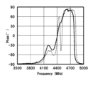
- FIGS. 4A to 4C show diagrams comparing the resonance characteristics of the elastic wave resonator 1 according to an example of the present invention and the resonance characteristics of an elastic wave resonator according to a comparative example.
- FIG. 4A is a diagram showing the entire resonance characteristic
- FIG. 4B is an enlarged diagram of the resonance due to the main mode
- FIG. 4C is a diagram showing the resonance due to the spurious mode enlarged.
- the solid line shows the characteristics of the example
- the dotted line shows the characteristics of the comparative example.
- the designs of the elastic wave resonator 1 according to an embodiment of the present invention and the elastic wave resonator according to a comparative example are as follows.
- Comparative example piezoelectric layer: LN, IDT electrode: Al, pitch: 2.18 ⁇ m, duty d: 0.3)
- the pitch of 2.12 ⁇ m to 2.42 ⁇ m means that the pitch increases continuously in one direction from 2.12 ⁇ m to 2.42 ⁇ m.
- the entire electrode finger arrangement region 7 belongs to the first region 71 in the embodiment.
- the elastic wave resonator 1 according to the embodiment of the present invention has reduced resonance due to spurious modes compared to the elastic wave resonator according to the comparative example.
- the main mode resonance has a smaller loss than the spurious mode, and still maintains good characteristics.
- the pitch of the plurality of electrode fingers 412 located in the first region 71 is not particularly limited as long as the pitches are different from each other.
- the pitches of the plurality of electrode fingers 412 located in the first region 71 may increase by the same amount or rate of increase toward the first direction (the direction in which the electrode fingers 412 are arranged).
- FIG. 5 is a diagram showing the pitch difference necessary to express a frequency difference of 50 MHz in a resonator with an anti-resonance frequency of 4600 MHz to 4950 MHz.
- the vertical axis represents the value of 100 ⁇ (Pmax-Pmin)/Pmax, where Pmax is the largest pitch among the pitches of the plurality of electrode fingers 412 located in the first region 71, and Pmin is the smallest pitch. It shows.
- the horizontal axis indicates the value of the duty d of the electrode finger 412 located in the first region 71.
- each plot represents the change in the thickness of LN in the range of 0.47 ⁇ m to 0.5 ⁇ m.
- the pitch of the plurality of electrode fingers 412 located in the first region 71 may be 100 ⁇ (Pmax ⁇ Pmin)/Pmax ⁇ 3.0.
- the difference between the maximum pitch and the minimum pitch of the plurality of electrode fingers 412 located in the first region 71 is 50 MHz or more, so that the resonance waveform due to the spurious mode is more effectively broadened. be able to. Thereby, for example, the influence on the pass characteristics of the filter can be reduced.
- the piezoelectric layer 2 is constituted by a 120° Y cut-X propagation LN, but the present invention is not limited to this example.
- the Euler angle of the piezoelectric layer 2 may be set as appropriate.
- the Euler angle of the piezoelectric layer 2 may be (0°, ⁇ + ( ⁇ ⁇ 180), 0°) ( ⁇ is any value in the range of 0° to 180°, and ⁇ is an integer from 0 to 2. ).
- the piezoelectric layer 2 may be formed of a Z-cut LN or LT. In this case, for example, thickness-shear waves can be effectively utilized.
- the thickness of the piezoelectric layer 2 that overlaps with the first region 71 may be constant in plan view. With such a configuration, it is possible to reduce the resonance loss of the plate wave used, and provide the elastic wave resonator 1 having good filter characteristics. Note that the term "the thickness of the piezoelectric layer 2 is constant" does not necessarily mean that it is strictly constant, but rather that it may vary slightly within a range that does not significantly affect the characteristics of the elastic waves propagating through the piezoelectric layer 2. Allow.
- the support substrate 3 has the configuration shown in FIG. 1, but is not limited to this example.
- the support substrate 3 may have a void 8 on the top surface.
- the piezoelectric layer 2 covers the gap 8 of the support substrate 3, leaving a space inside the gap 8 in a plan view. Note that the size and depth of the void 8 may be set as appropriate.
- the piezoelectric layer 2 and the support substrate 3 are in direct contact with each other, but the present invention is not limited to this example.
- the lower surface 2b of the piezoelectric layer 2 and the support substrate 3 may be in direct contact with each other, or may be in indirect contact with each other via, for example, an intermediate layer and an adhesive layer (not shown).
- Examples of such an intermediate layer include insulating materials such as silicon oxide (SiO 2 ), silicon nitride (Si 3 N 4 ), and aluminum oxide (Al 2 O 3 ). By providing such an insulating intermediate layer, it is possible to reduce the formation of unnecessary potential and unnecessary capacitance, and it is possible to improve the electrical characteristics of the acoustic wave resonator 1. .
- both an adhesive layer and an intermediate layer may be located between the piezoelectric layer 2 and the support substrate 3.
- the adhesive layer is located between the support substrate 3 and the intermediate layer.
- An example of such an adhesive layer is amorphous silicon.
- an alumina film (not shown) or the like may be further located between the intermediate layer and the piezoelectric layer 2.
- an alumina film (not shown) or the like may be further located between the intermediate layer and the piezoelectric layer 2.
- an alumina film it is possible to reduce the leakage of elastic waves from the piezoelectric layer 2 to the support substrate 3 side, and it is possible to improve the frequency characteristics of the elastic wave resonator 1.
- FIG. 6B shows a schematic cross-sectional view of an elastic wave resonator 1 according to yet another embodiment.
- a multilayer film layer 5 may be located between the piezoelectric layer 2 and the support substrate 3.
- low acoustic impedance layers 51 and high acoustic impedance layers 52 are alternately laminated.
- the acoustic impedance of the low acoustic impedance layer 51 is lower than that of the piezoelectric layer 2
- the acoustic impedance of the high acoustic impedance layer 52 is higher than that of the low acoustic impedance layer 51 .
- the low acoustic impedance layer 51 is silicon oxide (SiO 2 )
- the high acoustic impedance layer 52 is hafnium oxide (HfO 2 ).
- the duty d of the electrode fingers 412 located in the first region 71 may be constant. Since the pitches of the electrode fingers 412 located in the first region 71 are different from each other, when the value of the duty d of the electrode fingers 412 located in the first region 71 is constant, the expected value is lower than when the duty d is different. It is possible to reduce the possibility that spurious will occur due to resonance that was not present, and to effectively reduce spurious.
- the value of the duty d of the electrode finger 412 located in the first region 71 is 0.6 or less. Note that the constant value of the duty d does not necessarily mean that it is strictly constant, but allows for some variation within a range of, for example, 0.01 or less.
- the thickness of the electrode fingers 412 located in the first region 71 may be constant, or may be set to a different thickness for each electrode finger 412 as appropriate. good.
- the first region 71 may occupy half or more of the area of the electrode finger arrangement region 7, but the present invention is not limited to this example.
- the number of electrode fingers 412 located in the first region 71 may be half or more of the total number of the plurality of electrode fingers 412 located in the electrode finger arrangement region 7.
- the specific value of the number of electrode fingers 412 located in the first region 71 is not particularly limited. Theoretically, the number is 3 or more, which constitutes a pitch of 2 or more, and in practice, for example, it is 5 or more, 10 or more, 30 or more, 50 or more, or 100 or more. good.
- the pitches of all the electrode fingers 412 in the first region 71 may be different from each other, but the pitch is not limited to this example.
- the pitch of the electrode fingers 412 may increase toward one side in the first direction (the direction in which the electrode fingers 412 are arranged).
- the central region may include a portion where the pitch is constant.
- the pitch may not increase continuously in a part or all of the central region, but may increase stepwise (stepwise). Even in this case, effects such as broadening can still be obtained.
- the number of pitch changes in the central region is not particularly limited. Theoretically, the number of changes is 1 or more, and in practice, it may be, for example, 5 or more, 10 or more, 30 or more, 50 or more, or 100 or more.
- FIG. 7 is a circuit diagram schematically showing the configuration of an elastic wave filter 101 as an example of how the elastic wave resonator 1 is used.
- the comb-shaped electrode 41 is schematically shown in the form of a forked fork in this drawing, and the reflector 42 is a single piece with bent ends. It is represented by a line.
- the elastic wave filter 101 filters a signal input from the input terminal 102 and outputs the filtered signal to the output terminal 103.
- the elastic wave filter 101 is configured by, for example, a ladder type filter in which a plurality of resonators are connected in a ladder type. That is, the elastic wave filter 101 includes a plurality of resonators (series resonators) connected in series between an input terminal 102 and an output terminal 103, and a line in series with the reference potential. It has a plurality of (or even one) resonators (parallel resonators) to be connected.
- At least one of the resonators included in the elastic wave filter 101 in this embodiment is the elastic wave resonator 1 in this embodiment.
- a resonator made up of the elastic wave resonator 1 will be referred to as a first elastic wave resonator 11.
- the elastic wave filter 101 includes a second elastic wave resonator 12.
- the anti-resonant frequency of the second elastic wave resonator 12 is lower than the anti-resonant frequency of the first elastic wave resonator 11. may also be located near the passband of the elastic wave filter 101.
- the elastic wave filter 101 may be designed so that (P2max-P2min) is smaller than (P1max-P1min).
- the second elastic wave resonator 12 has a smaller pitch difference than the first elastic wave resonator 11.
- a resonator with a small pitch difference has less main mode resonance loss than a resonator with a large pitch difference. Therefore, between the anti-resonant frequency of the first elastic wave resonator 11 and the passband of the elastic wave filter 101, the anti-resonant frequency of the second elastic wave resonator 12, which has a pitch difference smaller than that of the first elastic wave resonator 11, is generated.
- the main mode of the resonator near the passband of the filter, the loss of the main mode of the resonator can be reduced. Therefore, it is possible to provide an elastic wave filter with highly steep filter characteristics.
- the resonant frequency of the second elastic wave resonator 12 is more elastic than the resonant frequency of the first elastic wave resonator 11. It may be located near the passband of wave filter 101.
- the elastic wave filter 101 may be designed so that (P2max-P2min) is smaller than (P1max-P1min).
- the second elastic wave resonator 12 has a smaller pitch difference than the first elastic wave resonator 11. Therefore, between the anti-resonant frequency of the first elastic wave resonator 11 and the passband of the elastic wave filter 101, the anti-resonant frequency of the second elastic wave resonator 12, which has a pitch difference smaller than that of the first elastic wave resonator 11, is generated.
- the main mode of the resonator near the passband of the filter, the loss of the main mode of the resonator can be reduced. Therefore, it is possible to provide an elastic wave filter with highly steep filter characteristics.
- the maximum phase of the spurious generated from the first elastic wave resonator 11 that exists in the pass band of the elastic wave filter 101 may be -70° or less. good.
- the maximum phase of the spurious generated from the first elastic wave resonator 11 that exists in the passband of the elastic wave filter 101 may be located in the range of ⁇ 80° to ⁇ 70°.
- a spurious signal with a small phase is located in the passband of the elastic wave filter 101, and the influence of the spurious signal on the filter can be reduced.
- the elastic wave filter 101 is a ladder type filter, it is not limited to this example.
- the elastic wave filter 101 may be a multimode filter (including a double mode filter).
- the multimode filter includes a plurality of IDT electrodes 4 arranged in the propagation direction of elastic waves and a pair of reflectors 42 arranged on both sides of the IDT electrodes 4.
- FIG. 8 is a block diagram showing main parts of a communication device 111 as an example of using the elastic wave resonator 1 and the elastic wave filter 101.
- the communication device 111 performs wireless communication using radio waves, and includes a duplexer 116.
- the duplexer 116 includes a transmission filter 101a and a reception filter 101b. At least one of the transmission filter 101a and the reception filter 101b is configured by an elastic wave filter 101. Both the output side of the transmission filter 101a and the input side of the reception filter 101b are connected to an antenna 112.
- a transmission information signal TIS containing information to be transmitted is modulated and frequency-increased (conversion of carrier frequency to a high-frequency signal) by an RF-IC (Radio Frequency Integrated Circuit) 113, and is converted into a transmission signal TS.
- the transmission signal TS has unnecessary components outside the transmission passband removed by the bandpass filter 115a, is amplified by the amplifier 114a, and is input to the duplexer 116 (transmission filter 101a). Then, the duplexer 116 (transmission filter 101a) removes unnecessary components outside the transmission passband from the input transmission signal TS, and outputs the removed transmission signal TS to the antenna 112.
- the antenna 112 converts the input electrical signal (transmission signal TS) into a wireless signal (radio wave) and transmits the signal.
- a wireless signal (radio wave) received by the antenna 112 is converted into an electric signal (received signal RS) by the antenna 112 and input to the duplexer 116 .
- the duplexer 116 (reception filter 101b) removes unnecessary components outside the reception passband from the input reception signal RS, and outputs the removed signal to the amplifier 114b.
- the output received signal RS is amplified by the amplifier 114b, and unnecessary components outside the receiving passband are removed by the bandpass filter 115b. Then, the received signal RS is lowered in frequency and demodulated by the RF-IC 113 to become a received information signal RIS.
- the transmission information signal TIS and the reception information signal RIS may be low frequency signals (baseband signals) containing appropriate information, such as analog audio signals or digitized audio signals.
- the passband of the wireless signal may be set as appropriate, and in this embodiment, a relatively high frequency passband (for example, 5 GHz or higher) is also possible.
- the modulation method may be phase modulation, amplitude modulation, frequency modulation, or a combination of two or more of these.
- the direct conversion system is illustrated as an example of the circuit system in FIG. 8, it may be any other suitable circuit system, for example, a double superheterodyne system. Further, FIG. 8 schematically shows only the main parts, and a low-pass filter or isolator or the like may be added at an appropriate position, or the position of an amplifier or the like may be changed.
Landscapes
- Physics & Mathematics (AREA)
- Acoustics & Sound (AREA)
- Surface Acoustic Wave Elements And Circuit Networks Thereof (AREA)
Abstract
Provided is an elastic wave resonator comprising a piezoelectric layer and an IDT electrode. The piezoelectric layer is piezoelectric. The IDT electrode is positioned on a first surface of the piezoelectric layer, and comprises a plurality of electrode fingers aligned in a first direction. The entire plurality of electrode fingers is positioned in an electrode finger arrangement region. The distance in the first direction from one side of one electrode finger to said one side of an electrode finger adjacent to the one electrode finger is defined as the pitch of the one electrode finger. The electrode finger arrangement region comprises a first region where the pitches of all of the electrode fingers differ from each other. The elastic wave resonator is configured to enable usage of plate waves or bulk waves as elastic waves that propagate through the electrode finger arrangement region.
Description
本発明は、弾性波を利用する電子部品である弾性波共振子、当該弾性波共振子を有する弾性波フィルタおよび通信装置に関する。
The present invention relates to an elastic wave resonator that is an electronic component that utilizes elastic waves, an elastic wave filter having the elastic wave resonator, and a communication device.
圧電基板の表面に設けた複数個の電極指で構成されるIDT(interdigital transducer)電極に電圧を印加して、圧電体を伝搬する弾性波を生じさせる弾性波共振子が知られている。IDT電極は、両端部において電極指ピッチを徐々に小さくしたグラデーション領域を有する構成からなる。このような構成とすることにより、リップルの小さい弾性表面波共振子を得ることができる。
An elastic wave resonator is known in which a voltage is applied to an IDT (interdigital transducer) electrode formed of a plurality of electrode fingers provided on the surface of a piezoelectric substrate to generate an elastic wave that propagates through a piezoelectric material. The IDT electrode has a gradation region in which the electrode finger pitch is gradually reduced at both ends. With such a configuration, a surface acoustic wave resonator with small ripples can be obtained.
本発明の一実施形態に係る弾性波共振子は、圧電体層と、IDT電極とを有する。前記圧電体層は、圧電性を有する。前記IDT電極は、前記圧電体層の第1面に位置し、第1方向に配列された複数の電極指を有する。前記複数の電極指の全体は、電極指配置領域に位置する。前記第1方向における、1つの電極指の一方の側から、当該1つの電極指に隣り合う電極指の前記一方の側までの距離を、当該1つの電極指のピッチと定義する。前記電極指配置領域は、全ての電極指のピッチが互いに異なる、第1領域を有する。前記弾性波共振子は、前記電極指配置領域を伝搬する弾性波として、板波またはバルク波を利用するように構成される。
An elastic wave resonator according to an embodiment of the present invention includes a piezoelectric layer and an IDT electrode. The piezoelectric layer has piezoelectricity. The IDT electrode is located on the first surface of the piezoelectric layer and has a plurality of electrode fingers arranged in a first direction. All of the plurality of electrode fingers are located in the electrode finger arrangement region. The distance from one side of one electrode finger to the one side of the electrode finger adjacent to the one electrode finger in the first direction is defined as the pitch of the one electrode finger. The electrode finger arrangement region has a first region in which all the electrode fingers have different pitches. The elastic wave resonator is configured to use a plate wave or a bulk wave as an elastic wave propagating in the electrode finger arrangement region.
本発明の一実施形態に係る弾性波共振子は、圧電体層と、IDT電極とを有する。前記圧電体層は、圧電性を有する。前記IDT電極は、前記圧電体層の第1面に位置し、第1方向に配列された複数の電極指を有する。前記複数の電極指の全体は、電極指配置領域に位置する。前記第1方向における、1つの電極指の一方の側から、当該1つの電極指に隣り合う電極指の前記一方の側までの距離を、当該1つの電極指のピッチと定義する。前記電極指配置領域を前記第1方向に3等分した場合における中央側領域では、前記一方の側へ向かうにつれて電極指のピッチが大きくなっている。
An elastic wave resonator according to an embodiment of the present invention includes a piezoelectric layer and an IDT electrode. The piezoelectric layer has piezoelectricity. The IDT electrode is located on the first surface of the piezoelectric layer and has a plurality of electrode fingers arranged in a first direction. All of the plurality of electrode fingers are located in the electrode finger arrangement region. The distance from one side of one electrode finger to the one side of the electrode finger adjacent to the one electrode finger in the first direction is defined as the pitch of the one electrode finger. In the central region where the electrode finger arrangement region is divided into three equal parts in the first direction, the pitch of the electrode fingers increases toward the one side.
本発明の一実施形態に係る弾性波フィルタは、直列に接続された複数の直列腕共振子と、前記直列腕共振子に並列に接続された並列腕共振子と、を有するラダー型の弾性波フィルタである。前記複数の直列共振子は、上記のいずれかに記載する弾性波共振子と、第2弾性波共振子を含む。前記第2弾性波共振子の反共振周波数は、前記弾性波共振子の反共振周波数よりも、前記弾性波フィルタの通過帯域の近くに位置する。前記弾性波共振子が有するIDT電極の複数の電極指のピッチのうち、最も大きいピッチをP1maxとし、最も小さいピッチをP1minと定義する。前記第2弾性波共振子が有するIDT電極の複数の電極指のピッチのうち、最も大きいピッチをP2maxとし、最も小さいピッチをP2minと定義する。(P2max-P2min)は(P1max-P1min)よりも小さい。
An elastic wave filter according to an embodiment of the present invention is a ladder-type elastic wave filter including a plurality of series arm resonators connected in series and a parallel arm resonator connected in parallel to the series arm resonators. It's a filter. The plurality of series resonators include any of the elastic wave resonators described above and a second elastic wave resonator. The anti-resonant frequency of the second elastic wave resonator is located closer to the passband of the elastic wave filter than the anti-resonant frequency of the elastic wave resonator. Among the pitches of the plurality of electrode fingers of the IDT electrode of the elastic wave resonator, the largest pitch is defined as P1max, and the smallest pitch is defined as P1min. Among the pitches of the plurality of electrode fingers of the IDT electrode of the second acoustic wave resonator, the largest pitch is defined as P2max, and the smallest pitch is defined as P2min. (P2max-P2min) is smaller than (P1max-P1min).
本発明の一実施形態に係る弾性波フィルタは、直列に接続された直列腕共振子と、前記直列腕共振子に並列に接続された複数の並列腕共振子と、を有するラダー型の弾性波フィルタである。前記複数の並列腕共振子は、上記のいずれかに記載する弾性波共振子と、第2弾性波共振子を含む。前記第2弾性波共振子の共振周波数は、前記弾性波共振子の共振周波数よりも、前記弾性波フィルタの通過帯域の近くに位置する。前記弾性波共振子が有するIDT電極の複数の電極指のピッチのうち、最も大きいピッチをP1maxとし、最も小さいピッチをP1minと定義する。前記第2弾性波共振子が有するIDT電極の複数の電極指のピッチのうち、最も大きいピッチをP2maxとし、最も小さいピッチをP2minと定義する。(P2max-P2min)は(P1max-P1min)よりも小さい。
An elastic wave filter according to an embodiment of the present invention is a ladder-type elastic wave filter including a series arm resonator connected in series and a plurality of parallel arm resonators connected in parallel to the series arm resonator. It's a filter. The plurality of parallel arm resonators include any of the elastic wave resonators described above and a second elastic wave resonator. The resonant frequency of the second elastic wave resonator is located closer to the passband of the elastic wave filter than the resonant frequency of the elastic wave resonator. Among the pitches of the plurality of electrode fingers of the IDT electrode of the elastic wave resonator, the largest pitch is defined as P1max, and the smallest pitch is defined as P1min. Among the pitches of the plurality of electrode fingers of the IDT electrode of the second acoustic wave resonator, the largest pitch is defined as P2max, and the smallest pitch is defined as P2min. (P2max-P2min) is smaller than (P1max-P1min).
本発明の一実施形態に係る弾性波フィルタは、上記のいずれかに記載する弾性波共振子を有する弾性波フィルタであって、前記弾性波フィルタの通過帯域に存在する、前記弾性波共振子に由来するスプリアスの最大位相は、-70°以下である。
An elastic wave filter according to an embodiment of the present invention is an elastic wave filter having an elastic wave resonator described in any one of the above, wherein the elastic wave resonator exists in a passband of the elastic wave filter. The maximum phase of the derived spurious is -70° or less.
本発明の一実施形態に係る通信装置は、アンテナと、前記アンテナに接続されている弾性波フィルタと、前記弾性波フィルタに接続されているICと、を有する。前記弾性波フィルタは、上記弾性波共振子を含む。
A communication device according to an embodiment of the present invention includes an antenna, an elastic wave filter connected to the antenna, and an IC connected to the elastic wave filter. The elastic wave filter includes the elastic wave resonator.
以下、本発明に係る実施形態について、図面を参照して説明する。なお、以下の説明で用いられる図は模式的なものであり、図面上の寸法比率等は現実のものとは必ずしも一致していない。
Hereinafter, embodiments according to the present invention will be described with reference to the drawings. Note that the drawings used in the following explanation are schematic, and the dimensional ratios, etc. in the drawings do not necessarily match the actual ones.
図面には、便宜上、X軸、Y軸およびZ軸からなる直交座標系を付すことがある。本発明に係る弾性波共振子1は、いずれの方向が上方または下方とされてもよい。ただし、便宜上、Z軸方向を上下方向として上面または下面の語を用いることがある。なお、X軸は、後述する圧電体層2の上面に沿って伝搬するSAW(Surface Acoustic Wave)の伝搬方向と平行になるように定義され、Y軸は、圧電体層2の上面に平行かつX軸に直交するように定義され、Z軸は、圧電体層2の上面に直交するように定義されている。
For convenience, an orthogonal coordinate system consisting of an X-axis, a Y-axis, and a Z-axis may be attached to the drawings. In the elastic wave resonator 1 according to the present invention, either direction may be upward or downward. However, for convenience, the term upper surface or lower surface may be used with the Z-axis direction as the vertical direction. Note that the X-axis is defined to be parallel to the propagation direction of SAW (Surface Acoustic Wave) that propagates along the upper surface of the piezoelectric layer 2, which will be described later, and the Y-axis is parallel to the upper surface of the piezoelectric layer 2 and It is defined to be perpendicular to the X-axis, and the Z-axis is defined to be perpendicular to the top surface of the piezoelectric layer 2.
なお、本明細書に記載する各実施形態は例示的なものであり、異なる実施形態間において部分的に置換してもよい。また、異なる実施形態を部分的に組み合わせてもよい。
Note that each embodiment described in this specification is an example, and different embodiments may be partially replaced. Also, different embodiments may be partially combined.
図1は本発明の一実施形態に係る弾性波共振子1の模式的な断面図である。
FIG. 1 is a schematic cross-sectional view of an elastic wave resonator 1 according to an embodiment of the present invention.
本発明の一実施形態に係る弾性波共振子1は、図1に示すように、圧電体層2と支持基板3と、IDT電極4を有している。支持基板3と圧電体層2は、この順に積層されている。
As shown in FIG. 1, an elastic wave resonator 1 according to an embodiment of the present invention includes a piezoelectric layer 2, a support substrate 3, and an IDT electrode 4. The support substrate 3 and the piezoelectric layer 2 are laminated in this order.
支持基板3は、その上に積層される圧電体層2を支持するものであり、支持基板3の材料は、一定の強度を備えれば特に限定されない。例えば、支持基板3が、圧電体層2に比べて線膨張係数の小さい材料で構成される場合には、温度変化による圧電体層2の変形を低減することで、温度変化による共振特性の変化を低減することができる。また、支持基板3の材料は、圧電体層2を伝搬する弾性波の横波音速に比べて、伝搬する弾性波の横波音速が大きい材料であってもよい。支持基板3の材料に、圧電体層2を伝搬する弾性波の横波音速に比べて、伝搬する弾性波の横波音速が大きい材料を選定した場合には、弾性波を圧電体層2に閉じ込めることができ、周波数特性の優れた弾性波共振子1を提供することができる。
The support substrate 3 supports the piezoelectric layer 2 laminated thereon, and the material of the support substrate 3 is not particularly limited as long as it has a certain strength. For example, if the support substrate 3 is made of a material with a smaller coefficient of linear expansion than the piezoelectric layer 2, it is possible to reduce the deformation of the piezoelectric layer 2 due to temperature changes, thereby changing the resonance characteristics due to temperature changes. can be reduced. Further, the material of the support substrate 3 may be a material in which the transverse wave sound velocity of the elastic wave propagating is higher than the transverse wave sound velocity of the elastic wave propagating through the piezoelectric layer 2 . If a material is selected for the support substrate 3 that has a higher transverse sound velocity of the elastic waves propagating in the piezoelectric layer 2 than the transverse sound velocity of the elastic waves propagating in the piezoelectric layer 2, the elastic waves can be confined in the piezoelectric layer 2. Therefore, it is possible to provide an elastic wave resonator 1 with excellent frequency characteristics.
このような材料として、例えば、サファイア(Al2O3)およびシリコン(Si)等を例示できる。本実施形態においては支持基板3としてSiを用いた場合を例に説明する。
Examples of such materials include sapphire (Al 2 O 3 ) and silicon (Si). In this embodiment, a case where Si is used as the support substrate 3 will be explained as an example.
支持基板3の厚みは、特に限定されないが、例えば、後述する圧電体層2の厚みよりも厚い。
The thickness of the support substrate 3 is not particularly limited, but is, for example, thicker than the thickness of the piezoelectric layer 2 described below.
圧電体層2は、Z軸を上下方向として、Z軸に垂直な上面2aと下面2bを備える。下面2b側には、前述の支持基板3が位置している。下面2bと、支持基板3は、直接的に接していてもよいし、例えば後述の中間層および多層膜層5等を介して間接的に接していてもよい。また、下面2bと、支持基板3は、不図示の接着層等を介して、間接的に接していてもよい。上面2a側には、後述のIDT電極4が位置している。
The piezoelectric layer 2 has an upper surface 2a and a lower surface 2b that are perpendicular to the Z-axis, with the Z-axis being the vertical direction. The aforementioned support substrate 3 is located on the lower surface 2b side. The lower surface 2b and the support substrate 3 may be in direct contact with each other, or may be in indirect contact with each other via, for example, an intermediate layer and a multilayer film layer 5, which will be described later. Further, the lower surface 2b and the support substrate 3 may be in indirect contact with each other via an adhesive layer (not shown) or the like. An IDT electrode 4, which will be described later, is located on the upper surface 2a side.
圧電体層2には、例えば、タンタル酸リチウム(LiTaO3;以下LTという)結晶からなる圧電性を有する単結晶の基板および、ニオブ酸リチウム(LiNbO3;以下LNという)結晶からなる圧電性を有する単結晶の基板等を用いることができる。本実施形態においては、具体的には、圧電体層2は120°Yカット-X伝搬のLNによって構成されている。
The piezoelectric layer 2 includes, for example, a piezoelectric single-crystal substrate made of lithium tantalate (LiTaO 3 ; hereinafter referred to as LT) crystal and a piezoelectric substrate made of lithium niobate (LiNbO 3 ; hereinafter referred to as LN) crystal. A single-crystal substrate having the same structure can be used. In this embodiment, specifically, the piezoelectric layer 2 is constituted by a 120° Y cut-X propagation LN.
後述するIDT電極4に高周波信号が印加されることにより、圧電体層2を弾性波の伝搬方向に伝搬する弾性波が励振される。伝搬方向は任意であり、例えば、圧電体層2の上面及び下面に沿う方向及び/又は圧電体層2の厚み方向であってよい。本実施形態の弾性波共振子1において、励振される弾性波には板波又はバルク波が含まれる。弾性波共振子1は、メインモードとして、板波を利用してもよいし、バルク波を利用してもよい。
By applying a high frequency signal to the IDT electrode 4, which will be described later, an elastic wave propagating through the piezoelectric layer 2 in the propagation direction of the elastic wave is excited. The propagation direction is arbitrary, and may be, for example, a direction along the upper and lower surfaces of the piezoelectric layer 2 and/or a direction along the thickness of the piezoelectric layer 2. In the elastic wave resonator 1 of this embodiment, the elastic waves excited include plate waves or bulk waves. The elastic wave resonator 1 may use a plate wave or a bulk wave as a main mode.
利用される弾性波の種類は特に限定されない。例えば板波は、Lamb波であってもよい。例えばバルク波は、SH波であってもよいし厚みすべり波であってもよい。また、利用される板波の伝搬モードは特に限定されない。具体的に、本実施形態において、板波はLamb波のA1モードである。
The type of elastic waves used is not particularly limited. For example, the plate wave may be a Lamb wave. For example, the bulk wave may be an SH wave or a thickness-shear wave. Further, the propagation mode of the plate wave to be used is not particularly limited. Specifically, in this embodiment, the plate wave is the A1 mode of the Lamb wave.
念のために記載すると、Lamb波は、電極指412の配列方向(伝搬方向)の成分(P成分)及び/又は圧電体層2の厚み方向の成分(SV成分)を主とする。A1モードは、非対称モード(Aモード)のうち、1次のもの(厚み方向における節の数が1つであるもの)を指す。SH波は、電極指412の配列方向(伝搬方向)に垂直で圧電体層2の表面に水平な方向の成分(SH成分)を主とする。厚みすべり波は、圧電体層2の厚み方向の互いに異なる部位(例えば上面及び下面)を圧電体層2の上面及び下面に沿う方向にスライドさせ、また、圧電体層2の厚み方向に伝搬する。厚みすべり波の次数は任意であり、例えば、1次(厚み方向における節の数が1つ)である。
To be sure, the Lamb wave mainly includes a component (P component) in the arrangement direction (propagation direction) of the electrode fingers 412 and/or a component (SV component) in the thickness direction of the piezoelectric layer 2. The A1 mode refers to a first-order mode (one having one node in the thickness direction) among the asymmetric modes (A mode). The SH wave mainly has a component (SH component) in a direction perpendicular to the arrangement direction (propagation direction) of the electrode fingers 412 and horizontal to the surface of the piezoelectric layer 2. The thickness shear wave causes different parts (for example, the upper surface and lower surface) of the piezoelectric layer 2 in the thickness direction to slide in a direction along the upper surface and the lower surface of the piezoelectric layer 2, and also propagates in the thickness direction of the piezoelectric layer 2. . The order of the thickness shear wave is arbitrary, for example, first order (the number of nodes in the thickness direction is one).
圧電体層2の厚みは、板波を利用できる厚みであれば適宜設定されてもよい。例えば、本実施形態においては、圧電体層2の厚みは、後述するλを用いて表すと、2λ以下である。
The thickness of the piezoelectric layer 2 may be set as appropriate as long as it allows the use of plate waves. For example, in this embodiment, the thickness of the piezoelectric layer 2 is 2λ or less when expressed using λ, which will be described later.
IDT電極4は、圧電体層2の上面2aに位置している。IDT電極4は、導電性を有する材料で構成されている。IDT電極4の材料には、例えばAl、Cu、Pt、Mo、Auもしくはこれらの合金等種々の導電性材料を採用することができ、さらに、これら複数の層を積層させて構成してもよい。また、IDT電極4が、複数層の積層体からなる場合には、積層界面に不図示の下地層を介在させてもよい。本実施形態において、具体的に、IDT電極4はAlである。
The IDT electrode 4 is located on the upper surface 2a of the piezoelectric layer 2. The IDT electrode 4 is made of a conductive material. The IDT electrode 4 can be made of various conductive materials such as Al, Cu, Pt, Mo, Au, or an alloy thereof, and may also be constructed by laminating a plurality of these layers. . Further, when the IDT electrode 4 is composed of a multilayer stack, a base layer (not shown) may be interposed at the interface between the stacks. In this embodiment, specifically, the IDT electrode 4 is made of Al.
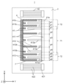
図2に、Z軸方向から平面視した時の、IDT電極4の形状を模式的に示す。図2に示すように、IDT電極4は、一対の櫛歯状電極41を含む。
FIG. 2 schematically shows the shape of the IDT electrode 4 when viewed in plan from the Z-axis direction. As shown in FIG. 2, the IDT electrode 4 includes a pair of comb-shaped electrodes 41. As shown in FIG.
櫛歯状電極41(41a及び41b)は、例えば、バスバー411(411a及び411b)と、該バスバー411から互いに伸びる複数の電極指412(412a及び412b)を含み、一方のバスバー411aに接続される電極指412aと、他方のバスバー411bに接続される電極指412bとが互いにかみ合うように配置されている。また、櫛歯状電極41は、複数の電極指412のそれぞれの間において、一方のバスバー411から突出し、他方のバスバー411から延びる電極指412と対向する、複数のダミー電極指413(413a及び413b)を含んでいてもよい。
The comb-shaped electrodes 41 (41a and 41b) include, for example, a busbar 411 (411a and 411b) and a plurality of electrode fingers 412 (412a and 412b) mutually extending from the busbar 411, and are connected to one busbar 411a. The electrode finger 412a and the electrode finger 412b connected to the other bus bar 411b are arranged so as to mesh with each other. Moreover, the comb-shaped electrode 41 protrudes from one bus bar 411 between each of the plurality of electrode fingers 412 and faces the electrode finger 412 extending from the other bus bar 411. ) may be included.
複数の電極指412のY軸方向の長さは、要求される電気特性等に応じて適宜に設定されてよい。例えば、複数の電極指412のY軸方向の長さは、互いに同等である。なお、IDT電極4は、複数の電極指412のY軸方向の長さ(別の観点では交差幅)が伝搬方向の位置に応じて変化する、いわゆるアポダイズが施されていてもよい。
The length of the plurality of electrode fingers 412 in the Y-axis direction may be set as appropriate depending on the required electrical characteristics and the like. For example, the lengths of the plurality of electrode fingers 412 in the Y-axis direction are equal to each other. Note that the IDT electrode 4 may be subjected to so-called apodization, in which the length of the plurality of electrode fingers 412 in the Y-axis direction (from another viewpoint, the intersection width) changes depending on the position in the propagation direction.
弾性波共振子1は、さらに、圧電体層2の上面に1対の反射器42を有していてもよい。1対の反射器42は、弾性波の伝搬方向において、IDT電極4の両側に位置している。反射器42は、互いに対向する1対の反射器バスバー421と、1対の反射器バスバー421間において延びる複数のストリップ電極422と、を含んでいる。
The elastic wave resonator 1 may further include a pair of reflectors 42 on the top surface of the piezoelectric layer 2. The pair of reflectors 42 are located on both sides of the IDT electrode 4 in the propagation direction of the elastic wave. The reflector 42 includes a pair of reflector bus bars 421 facing each other and a plurality of strip electrodes 422 extending between the pair of reflector bus bars 421.
複数の電極指412のZ軸方向における厚さは、要求される電気特性等に応じて適宜に設定されてよい。例えば、複数の電極指412のZ軸方向における厚みは一定であってもよい。
The thickness of the plurality of electrode fingers 412 in the Z-axis direction may be set as appropriate depending on the required electrical characteristics and the like. For example, the thickness of the plurality of electrode fingers 412 in the Z-axis direction may be constant.
図1に示すように、一つの電極指412aのX軸方向における幅を、電極指412aの幅(w)と定義する。また、電極指412aの一方の側から、電極指412aに隣り合う電極指412bの一方の側までの距離を、電極指412aのピッチ(p)と定義する。電極指412aのデューティーdは、電極指412aにおけるピッチに対する幅の比率を表すものである。つまり、電極指412aのデューティーdは、幅/ピッチ(w/p)で表すことができる。
As shown in FIG. 1, the width of one electrode finger 412a in the X-axis direction is defined as the width (w) of the electrode finger 412a. Further, the distance from one side of the electrode finger 412a to one side of the electrode finger 412b adjacent to the electrode finger 412a is defined as the pitch (p) of the electrode finger 412a. The duty d of the electrode finger 412a represents the ratio of the width to the pitch of the electrode finger 412a. In other words, the duty d of the electrode fingers 412a can be expressed as width/pitch (w/p).
複数の電極指412のそれぞれは、互いに所定のピッチに基づく間隔を空けて、配置されている。また、圧電体層2を伝搬する弾性波のうち、弾性波共振子1によって励振される弾性波が有する共振周波数は、電極指412のピッチに依存する。
Each of the plurality of electrode fingers 412 is arranged at intervals based on a predetermined pitch. Further, among the elastic waves propagating through the piezoelectric layer 2 , the resonance frequency of the elastic waves excited by the elastic wave resonator 1 depends on the pitch of the electrode fingers 412 .
本実施形態における弾性波共振子1において、図2に示すように、IDT電極4の複数の電極指412の全体は、平面視において、電極指配置領域7内に位置する。換言すると、電極指配置領域7は、平面視において、複数の電極指412の全体が位置する領域である。図2では、便宜上、電極指配置領域7を点線で示している。本実施形態において、電極指配置領域7は、第1領域71を少なくとも一つ含む。
In the elastic wave resonator 1 in this embodiment, as shown in FIG. 2, the plurality of electrode fingers 412 of the IDT electrode 4 are entirely located within the electrode finger arrangement region 7 in plan view. In other words, the electrode finger arrangement area 7 is an area where all of the plurality of electrode fingers 412 are located in plan view. In FIG. 2, the electrode finger arrangement region 7 is shown by dotted lines for convenience. In this embodiment, the electrode finger arrangement region 7 includes at least one first region 71.
本実施形態において、第1領域71に位置する全ての電極指412のピッチは、互いに異なっている。具体的には、図2において、第1領域71に位置するすべての電極指のピッチP1~P6は、互いに異なる。このように、電極指412のピッチが互いに異なることにより、2倍波および3倍波等を含む、種々の不要波の共振が低減され、スプリアスの発生を低減することができる。
In this embodiment, the pitches of all the electrode fingers 412 located in the first region 71 are different from each other. Specifically, in FIG. 2, the pitches P1 to P6 of all the electrode fingers located in the first region 71 are different from each other. In this way, since the pitches of the electrode fingers 412 are different from each other, resonance of various unnecessary waves including second harmonic waves, third harmonic waves, etc. can be reduced, and the occurrence of spurious waves can be reduced.
なお、本明細書において、第1領域に位置する複数の電極指のピッチのうち、最も大きいピッチの2倍をλと定義する。一般に、λは、波長を表す記号として用いられることが多い。ただし、弾性波共振子1において、板波の波長は、λと同等の大きさであってもよいし、同等の大きさでなくてもよい。例えば、A1モードのLamb波の波長は、比較的λに近くなりやすい。一方、厚みすべり波の波長は、λに対する依存性を有するが、圧電体層2の厚さに対する依存性が相対的に大きく、λに近いとは限らない。
Note that in this specification, λ is defined as twice the largest pitch among the pitches of the plurality of electrode fingers located in the first region. Generally, λ is often used as a symbol representing wavelength. However, in the elastic wave resonator 1, the wavelength of the plate wave may or may not be the same size as λ. For example, the wavelength of the Lamb wave in A1 mode tends to be relatively close to λ. On the other hand, the wavelength of the thickness shear wave has a dependence on λ, but the dependence on the thickness of the piezoelectric layer 2 is relatively large and is not necessarily close to λ.
また、本実施形態において、電極指配置領域7は、第2領域72を含んでいてもよい。第2領域72に位置する全ての電極指412のピッチは同一である。なお、本明細書において「ピッチが一定」とは、必ずしもが厳密に一定であることを指さず、製造誤差と呼べる範囲において多少の変動を許容する。製造誤差と呼べる範囲とは、例えば、その領域に位置する電極指412のピッチの平均値に対し、1.5%以下の範囲をいう。ただし、例えば、隣り合うピッチの差が上記の1.5%以下であっても、上記の隣り合うピッチを含む領域におけるピッチの変化傾向等を踏まえて総合的に判断したときに、ピッチを一定にすることが意図されていないことが明らかな場合は、上記の隣り合うピッチについて、ピッチが一定であると捉える必要はない。
Furthermore, in this embodiment, the electrode finger arrangement region 7 may include a second region 72. All the electrode fingers 412 located in the second region 72 have the same pitch. Note that in this specification, "the pitch is constant" does not necessarily mean that it is strictly constant, but allows for some variation within a range that can be called manufacturing error. The range that can be called a manufacturing error is, for example, a range of 1.5% or less with respect to the average value of the pitch of the electrode fingers 412 located in that region. However, for example, even if the difference between adjacent pitches is less than 1.5% as mentioned above, when comprehensively judged based on the tendency of pitch change in the area including the adjacent pitches, etc., the pitch can be kept constant. If it is clear that the pitch is not intended to be constant, it is not necessary to consider the above-mentioned adjacent pitches to be constant.
第1領域71と第2領域72の境界に位置する電極指412は、第1領域と第2領域の両方に含まれると解釈してもよい。後述する中央側領域とその両側の領域との境界に位置する電極指412についても同様に、中央側領域に含まれると解釈されてよい。
The electrode finger 412 located at the boundary between the first region 71 and the second region 72 may be interpreted as being included in both the first region and the second region. Electrode fingers 412 located at the boundary between the center region and regions on both sides thereof, which will be described later, may be similarly interpreted as being included in the center region.
本実施形態の弾性波共振子1は、板波をメインモードとして利用する。板波の共振特性は圧電体層2の厚みに大きく依存する。一方で、板波の共振は、電極指412のピッチが異なることによる影響を受けにくい。したがって、本実施形態では、弾性波共振子1が板波を利用し、第1領域71に位置する全ての電極指412のピッチが互いに異なることにより、板波によるメインモードの共振を比較的良好に保ちつつ、不要波によるスプリアスモードの共振を効果的に低減することができる。なお、板波をメインモードとして利用するとは、IDT電極4によって励振される弾性波のメインモードが板波であるということである。
The elastic wave resonator 1 of this embodiment uses plate waves as a main mode. The resonance characteristics of the plate wave largely depend on the thickness of the piezoelectric layer 2. On the other hand, the resonance of the plate wave is not easily affected by the difference in the pitch of the electrode fingers 412. Therefore, in this embodiment, since the elastic wave resonator 1 uses plate waves and the pitches of all the electrode fingers 412 located in the first region 71 are different from each other, the resonance of the main mode due to the plate waves can be achieved relatively well. It is possible to effectively reduce the resonance of spurious modes caused by unnecessary waves while maintaining the Note that using a plate wave as the main mode means that the main mode of the elastic wave excited by the IDT electrode 4 is a plate wave.
図2に示すように、第1領域71は、電極指配置領域7の半分以上の面積を占めていてもよい。このような構成とすることで、電極指412のピッチが異なる領域が支配的となり、より効果的に、位相の大きなスプリアスの発生を低減することができる。
As shown in FIG. 2, the first region 71 may occupy half or more of the area of the electrode finger arrangement region 7. With such a configuration, the regions in which the electrode fingers 412 have different pitches become dominant, and it is possible to more effectively reduce the occurrence of spurious signals with large phases.
また、図2に示すように、電極指412の配列方向における、電極指配置領域7の中央近傍は、第1領域71に属していてもよい。なお中央近傍とは、例えば、電極指配置領域7を電極指412の配列方向に3等分した場合における中央側の領域のことである。
Further, as shown in FIG. 2, the vicinity of the center of the electrode finger arrangement region 7 in the arrangement direction of the electrode fingers 412 may belong to the first region 71. Note that the vicinity of the center refers to, for example, a region on the center side when the electrode finger arrangement region 7 is divided into three equal parts in the arrangement direction of the electrode fingers 412.
また、図3に示すように、電極指配置領域7の全体が第1領域71に属していてもよい。このような構成とすることで、スプリアスの発生を低減させる領域が占める割合がさらに大きくなり、より効果的に、スプリアスの発生を低減することができる。
Furthermore, as shown in FIG. 3, the entire electrode finger arrangement region 7 may belong to the first region 71. With such a configuration, the area occupied by the area in which the generation of spurious waves is reduced becomes larger, and the generation of spurious waves can be reduced more effectively.
図4A~図4Cに本発明の一実施例に係る弾性波共振子1の共振特性と、比較例に係る弾性波共振子の共振特性を、比較した図を示す。図4Aは、共振特性全体を示した図であり、図4Bは、メインモードによる共振を拡大した図であり、図4Cは、スプリアスモードによる共振を拡大した図である。図中、実線は実施例の特性を示し、点線は比較例の特性を示す。
FIGS. 4A to 4C show diagrams comparing the resonance characteristics of the elastic wave resonator 1 according to an example of the present invention and the resonance characteristics of an elastic wave resonator according to a comparative example. FIG. 4A is a diagram showing the entire resonance characteristic, FIG. 4B is an enlarged diagram of the resonance due to the main mode, and FIG. 4C is a diagram showing the resonance due to the spurious mode enlarged. In the figure, the solid line shows the characteristics of the example, and the dotted line shows the characteristics of the comparative example.
本発明の一実施例に係る弾性波共振子1と比較例に係る弾性波共振子の設計は、それぞれ以下のとおりである。
実施例(圧電体層:LN、IDT電極:Al、ピッチ:2.12μm~2.42μm、デューティーd:0.3)
比較例(圧電体層:LN、IDT電極:Al、ピッチ:2.18μm、デューティーd:0.3) The designs of theelastic wave resonator 1 according to an embodiment of the present invention and the elastic wave resonator according to a comparative example are as follows.
Example (piezoelectric layer: LN, IDT electrode: Al, pitch: 2.12 μm to 2.42 μm, duty d: 0.3)
Comparative example (piezoelectric layer: LN, IDT electrode: Al, pitch: 2.18 μm, duty d: 0.3)
実施例(圧電体層:LN、IDT電極:Al、ピッチ:2.12μm~2.42μm、デューティーd:0.3)
比較例(圧電体層:LN、IDT電極:Al、ピッチ:2.18μm、デューティーd:0.3) The designs of the
Example (piezoelectric layer: LN, IDT electrode: Al, pitch: 2.12 μm to 2.42 μm, duty d: 0.3)
Comparative example (piezoelectric layer: LN, IDT electrode: Al, pitch: 2.18 μm, duty d: 0.3)
なお上記した実施例の設計値において、ピッチが2.12μm~2.42μmとあるのは、2.12μmから2.42μmまで一方向に連続的に増加することを意味している。このとき、ピッチは互いに異なる値であるため、実施例においては、電極指配置領域7の全体が第1領域71に属している。
Note that in the design values of the above-mentioned embodiments, the pitch of 2.12 μm to 2.42 μm means that the pitch increases continuously in one direction from 2.12 μm to 2.42 μm. At this time, since the pitches have different values, the entire electrode finger arrangement region 7 belongs to the first region 71 in the embodiment.
図4A~図4Cに示すように、本発明の一実施例に係る弾性波共振子1は、比較例に係る弾性波共振子に比べて、スプリアスモードによる共振が低減されている。一方で、メインモードによる共振は、スプリアスモードに比べてロスが小さく、依然として良好な特性を保っている。
As shown in FIGS. 4A to 4C, the elastic wave resonator 1 according to the embodiment of the present invention has reduced resonance due to spurious modes compared to the elastic wave resonator according to the comparative example. On the other hand, the main mode resonance has a smaller loss than the spurious mode, and still maintains good characteristics.
第1領域71に位置する複数の電極指412のピッチは、互いに異なる値であれば特に限定されない。一例として、第1領域71に位置する複数の電極指412のピッチは、第1方向(電極指412の配列方向)に向かって同じ増加量または同じ増加率で増加してもよい。
The pitch of the plurality of electrode fingers 412 located in the first region 71 is not particularly limited as long as the pitches are different from each other. As an example, the pitches of the plurality of electrode fingers 412 located in the first region 71 may increase by the same amount or rate of increase toward the first direction (the direction in which the electrode fingers 412 are arranged).
例えば、第1領域71に位置する複数の電極指412のピッチの増加量または増加率にばらつきがある場合、ピッチ差が小さい部分が含まれてしまい、当該ピッチ差が小さい部分に対応する周波数のスプリアスの強度が大きくなってしまう。一方で、複数の電極指412のピッチが、同じ増加量または同じ増加率で増加する場合、ピッチ差が均等になるため、スプリアスモードによる共振の波形を効果的にブロードニングさせることができる。これにより、例えばフィルタの通過特性への影響を低減することができる。
For example, if there is variation in the amount or rate of increase in the pitch of the plurality of electrode fingers 412 located in the first region 71, a portion with a small pitch difference will be included, and the frequency corresponding to the portion with a small pitch difference will be The intensity of spurious signals increases. On the other hand, when the pitches of the plurality of electrode fingers 412 increase by the same amount or the same rate of increase, the pitch difference becomes equal, so that the resonance waveform due to the spurious mode can be effectively broadened. Thereby, for example, the influence on the pass characteristics of the filter can be reduced.
図5は、反共振周波数が4600MHz~4950MHzの共振子において、50MHzの周波数差を表すのに必要なピッチ差を示した図である。縦軸は、第1領域71に位置する複数の電極指412のピッチのうち、最も大きいピッチをPmaxとし、最も小さいピッチをPminとした時の、100×(Pmax-Pmin)/Pmaxの値を示している。横軸は、第1領域71に位置する電極指412のデューティーdの値を示している。また、各プロットは、0.47μm~0.5μmの範囲におけるLNの厚みの変化を表している。
FIG. 5 is a diagram showing the pitch difference necessary to express a frequency difference of 50 MHz in a resonator with an anti-resonance frequency of 4600 MHz to 4950 MHz. The vertical axis represents the value of 100×(Pmax-Pmin)/Pmax, where Pmax is the largest pitch among the pitches of the plurality of electrode fingers 412 located in the first region 71, and Pmin is the smallest pitch. It shows. The horizontal axis indicates the value of the duty d of the electrode finger 412 located in the first region 71. Furthermore, each plot represents the change in the thickness of LN in the range of 0.47 μm to 0.5 μm.
例えば、第1領域71に位置する複数の電極指412のピッチは、100×(Pmax-Pmin)/Pmax≧3.0であってもよい。このような構成とすることで、第1領域71に位置する複数の電極指412の最大ピッチと最小ピッチの差が50MHz以上となるため、スプリアスモードによる共振波形を、より効果的にブロードニングさせることができる。これにより、例えばフィルタの通過特性への影響を低減することができる。
For example, the pitch of the plurality of electrode fingers 412 located in the first region 71 may be 100×(Pmax−Pmin)/Pmax≧3.0. With this configuration, the difference between the maximum pitch and the minimum pitch of the plurality of electrode fingers 412 located in the first region 71 is 50 MHz or more, so that the resonance waveform due to the spurious mode is more effectively broadened. be able to. Thereby, for example, the influence on the pass characteristics of the filter can be reduced.
本発明の一実施形態に係る弾性波共振子1において、圧電体層2は120°Yカット-X伝搬のLNによって構成されていると説明したが、この例に限定されない。圧電体層2のオイラー角は適宜設定されてもよい。例えば、圧電体層2のオイラー角は、(0°,θ+(α×180),0°)としてもよい(θは0°~180°の範囲で任意の値、αは0~2の整数)。圧電体層2が、このようなオイラー角の場合、効果的にLamb波のA1モードを利用することができる。また、例えば、圧電体層2は、ZカットのLN又はLTによって構成されていてもよい。この場合は、例えば、効果的に厚みすべり波を利用することができる。
In the elastic wave resonator 1 according to an embodiment of the present invention, it has been described that the piezoelectric layer 2 is constituted by a 120° Y cut-X propagation LN, but the present invention is not limited to this example. The Euler angle of the piezoelectric layer 2 may be set as appropriate. For example, the Euler angle of the piezoelectric layer 2 may be (0°, θ + (α × 180), 0°) (θ is any value in the range of 0° to 180°, and α is an integer from 0 to 2. ). When the piezoelectric layer 2 has such an Euler angle, the A1 mode of the Lamb wave can be effectively utilized. Further, for example, the piezoelectric layer 2 may be formed of a Z-cut LN or LT. In this case, for example, thickness-shear waves can be effectively utilized.
本発明の一実施形態に係る弾性波共振子1において、平面視で、第1領域71と重なる圧電体層2の厚みは、一定であってもよい。このような構成とすることで、利用される板波の共振のロスが低減され、良好なフィルタ特性を有する弾性波共振子1を提供することができる。なお、圧電体層2の厚みが一定であるとは、必ずしも厳密に一定であることを指さず、圧電体層2を伝搬する弾性波の特性に著しい影響を与えない範囲において多少の変動を許容する。
In the elastic wave resonator 1 according to an embodiment of the present invention, the thickness of the piezoelectric layer 2 that overlaps with the first region 71 may be constant in plan view. With such a configuration, it is possible to reduce the resonance loss of the plate wave used, and provide the elastic wave resonator 1 having good filter characteristics. Note that the term "the thickness of the piezoelectric layer 2 is constant" does not necessarily mean that it is strictly constant, but rather that it may vary slightly within a range that does not significantly affect the characteristics of the elastic waves propagating through the piezoelectric layer 2. Allow.
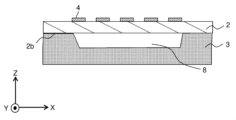
本発明の一実施形態に係る弾性波共振子1において、支持基板3は、図1に記載の構成としたが、この例に限定されない。例えば、図6Aに示した別の実施形態のように、支持基板3は、上面に空隙8を有していてもよい。この時、圧電体層2は支持基板3の空隙8を、空隙8の内部の空間を空けて、平面視で覆っている。なお、空隙8の大きさ、および深さは適宜に設定されてもよい。
In the elastic wave resonator 1 according to an embodiment of the present invention, the support substrate 3 has the configuration shown in FIG. 1, but is not limited to this example. For example, as in another embodiment shown in FIG. 6A, the support substrate 3 may have a void 8 on the top surface. At this time, the piezoelectric layer 2 covers the gap 8 of the support substrate 3, leaving a space inside the gap 8 in a plan view. Note that the size and depth of the void 8 may be set as appropriate.
図1に記載の、本発明の一実施形態に係る弾性波共振子1において、圧電体層2と支持基板3が直接接する例を示したが、この例に限定されない。圧電体層2の下面2bと支持基板3は、直接的に接していてもよいし、例えば、不図示の中間層および接着層等を介して、間接的に接していてもよい。
In the elastic wave resonator 1 according to an embodiment of the present invention shown in FIG. 1, an example is shown in which the piezoelectric layer 2 and the support substrate 3 are in direct contact with each other, but the present invention is not limited to this example. The lower surface 2b of the piezoelectric layer 2 and the support substrate 3 may be in direct contact with each other, or may be in indirect contact with each other via, for example, an intermediate layer and an adhesive layer (not shown).
このような中間層として、酸化ケイ素(SiO2)、窒化ケイ素(Si3N4)、酸化アルミニウム(Al2O3)等の絶縁性材料が例示できる。このような絶縁性の中間層を設けることにより、不要の電位が形成されたり不要の容量が形成されたりすることを低減することができ、弾性波共振子1の電気特性を向上させることができる。
Examples of such an intermediate layer include insulating materials such as silicon oxide (SiO 2 ), silicon nitride (Si 3 N 4 ), and aluminum oxide (Al 2 O 3 ). By providing such an insulating intermediate layer, it is possible to reduce the formation of unnecessary potential and unnecessary capacitance, and it is possible to improve the electrical characteristics of the acoustic wave resonator 1. .
また、圧電体層2と支持基板3の間に、接着層と中間層の両方が位置していてもよい。例えば、圧電体層2と支持基板3の間に、接着層と中間層の両方が位置する場合、接着層は支持基板3と中間層の間に位置する。このような接着層としてアモルファスシリコン等が例示できる。
Furthermore, both an adhesive layer and an intermediate layer may be located between the piezoelectric layer 2 and the support substrate 3. For example, when both the adhesive layer and the intermediate layer are located between the piezoelectric layer 2 and the support substrate 3, the adhesive layer is located between the support substrate 3 and the intermediate layer. An example of such an adhesive layer is amorphous silicon.
また一例として、中間層と圧電体層2との間に、さらに不図示のアルミナ膜等が位置していてもよい。このようなアルミナ膜が存在する場合、圧電体層2の弾性波が支持基板3側に漏洩することを低減でき、弾性波共振子1の周波数特性を向上することができる。
As an example, an alumina film (not shown) or the like may be further located between the intermediate layer and the piezoelectric layer 2. When such an alumina film is present, it is possible to reduce the leakage of elastic waves from the piezoelectric layer 2 to the support substrate 3 side, and it is possible to improve the frequency characteristics of the elastic wave resonator 1.
図6Bには、さらに別の実施形態に係る弾性波共振子1の模式的な断面図を示している。図6Bに示す実施形態においては、圧電体層2と支持基板3の間に、多層膜層5が位置していてもよい。多層膜層5は、低音響インピーダンス層51と高音響インピーダンス層52とが交互に積層している。低音響インピーダンス層51の音響インピーダンスは、圧電体層2の音響インピーダンスよりも低く、高音響インピーダンス層52の音響インピーダンスは、低音響インピーダンス層51の音響インピーダンスよりも高い。例えば、低音響インピーダンス層51は、酸化ケイ素(SiO2)であり、高音響インピーダンス層52は、酸化ハフニウム(HfO2)である。
FIG. 6B shows a schematic cross-sectional view of an elastic wave resonator 1 according to yet another embodiment. In the embodiment shown in FIG. 6B, a multilayer film layer 5 may be located between the piezoelectric layer 2 and the support substrate 3. In the multilayer film layer 5, low acoustic impedance layers 51 and high acoustic impedance layers 52 are alternately laminated. The acoustic impedance of the low acoustic impedance layer 51 is lower than that of the piezoelectric layer 2 , and the acoustic impedance of the high acoustic impedance layer 52 is higher than that of the low acoustic impedance layer 51 . For example, the low acoustic impedance layer 51 is silicon oxide (SiO 2 ), and the high acoustic impedance layer 52 is hafnium oxide (HfO 2 ).
本発明の一実施形態に係る弾性波共振子1において、第1領域71に位置する電極指412のデューティーdは、一定であってもよい。第1領域71に位置する電極指412のピッチは互いに異なるため、第1領域71に位置する電極指412のデューティーdの値が一定である場合は、デューティーdが異なる場合に比べて、想定しなかった共振によりスプリアスが発生する可能性を低減し、効果的にスプリアスを低減することができる。例えば、第1領域71に位置する電極指412のデューティーdの値は、0.6以下である。なお、デューティーdの値が一定であるとは、必ずしも厳密に一定であることを指さず、例えば0.01以下の範囲において多少の変動を許容する。
In the elastic wave resonator 1 according to an embodiment of the present invention, the duty d of the electrode fingers 412 located in the first region 71 may be constant. Since the pitches of the electrode fingers 412 located in the first region 71 are different from each other, when the value of the duty d of the electrode fingers 412 located in the first region 71 is constant, the expected value is lower than when the duty d is different. It is possible to reduce the possibility that spurious will occur due to resonance that was not present, and to effectively reduce spurious. For example, the value of the duty d of the electrode finger 412 located in the first region 71 is 0.6 or less. Note that the constant value of the duty d does not necessarily mean that it is strictly constant, but allows for some variation within a range of, for example, 0.01 or less.
本発明の一実施形態に係る弾性波共振子1において、第1領域71に位置する電極指412の厚みは、一定であってもよいし、電極指412ごとに異なる厚みで適宜設定されてもよい。
In the elastic wave resonator 1 according to the embodiment of the present invention, the thickness of the electrode fingers 412 located in the first region 71 may be constant, or may be set to a different thickness for each electrode finger 412 as appropriate. good.
本発明の一実施形態に係る弾性波共振子1において、第1領域71は、電極指配置領域7の半分以上の面積を占めていてもよいとしたが、この例に限定されない。例えば、第1領域71に位置する電極指412の本数は、電極指配置領域7に位置する複数の電極指412の総本数の半分以上の本数であってもよい。このような構成とすることで、電極指412のピッチが異なる領域が支配的となり、より効果的に、スプリアスの発生を低減することができる。
In the elastic wave resonator 1 according to the embodiment of the present invention, the first region 71 may occupy half or more of the area of the electrode finger arrangement region 7, but the present invention is not limited to this example. For example, the number of electrode fingers 412 located in the first region 71 may be half or more of the total number of the plurality of electrode fingers 412 located in the electrode finger arrangement region 7. With such a configuration, the regions in which the electrode fingers 412 have different pitches become dominant, and it is possible to more effectively reduce the occurrence of spurious noise.
第1領域71に位置する電極指412の本数の具体的な値は特に限定されない。当該本数は、理論上は、2以上のピッチが構成される3本以上であり、実用上は、例えば、5本以上、10本以上、30本以上、50本以上又は100本以上とされてよい。
The specific value of the number of electrode fingers 412 located in the first region 71 is not particularly limited. Theoretically, the number is 3 or more, which constitutes a pitch of 2 or more, and in practice, for example, it is 5 or more, 10 or more, 30 or more, 50 or more, or 100 or more. good.
本発明の一実施形態に係る弾性波共振子1において、第1領域71の全ての電極指412のピッチが互いに異なっていてもよいとしたが、この例に限定されない。例えば、電極指配置領域7を3等分した場合における中央側領域では、第1方向(電極指412の配列方向)の一方の側へ向かうにつれて、電極指412のピッチが大きくなっていてよい。このようにいうとき、中央側領域は、ピッチが一定の部分を含んでいても構わない。別の観点では、中央側領域の一部又は全部において、ピッチは、連続的に大きくなっていくのではなく、段階的(階段状)に大きくなっていってもよい。この場合であっても、ブロードニング等の効果が得られることに変わりはない。
In the elastic wave resonator 1 according to the embodiment of the present invention, the pitches of all the electrode fingers 412 in the first region 71 may be different from each other, but the pitch is not limited to this example. For example, in the central region when the electrode finger arrangement region 7 is divided into three equal parts, the pitch of the electrode fingers 412 may increase toward one side in the first direction (the direction in which the electrode fingers 412 are arranged). In this case, the central region may include a portion where the pitch is constant. From another point of view, the pitch may not increase continuously in a part or all of the central region, but may increase stepwise (stepwise). Even in this case, effects such as broadening can still be obtained.
中央側領域におけるピッチの変化の回数は特に限定されない。当該変化の回数は、理論上は、1以上であり、実用上は、例えば、5回以上、10回以上、30回以上、50回以上又は100回以上とされてよい。
The number of pitch changes in the central region is not particularly limited. Theoretically, the number of changes is 1 or more, and in practice, it may be, for example, 5 or more, 10 or more, 30 or more, 50 or more, or 100 or more.
(弾性波共振子1の利用例:弾性波フィルタ)
図7は、弾性波共振子1の利用例としての弾性波フィルタ101の構成を模式的に示す回路図である。この図の紙面左上に示された符号から理解されるように、この図では、櫛歯状電極41が二叉のフォーク形状によって模式的に示され、反射器42は両端が屈曲した1本の線で表わされている。 (Example of use of elastic wave resonator 1: elastic wave filter)
FIG. 7 is a circuit diagram schematically showing the configuration of anelastic wave filter 101 as an example of how the elastic wave resonator 1 is used. As can be understood from the reference numerals shown at the top left of the drawing, the comb-shaped electrode 41 is schematically shown in the form of a forked fork in this drawing, and the reflector 42 is a single piece with bent ends. It is represented by a line.
図7は、弾性波共振子1の利用例としての弾性波フィルタ101の構成を模式的に示す回路図である。この図の紙面左上に示された符号から理解されるように、この図では、櫛歯状電極41が二叉のフォーク形状によって模式的に示され、反射器42は両端が屈曲した1本の線で表わされている。 (Example of use of elastic wave resonator 1: elastic wave filter)
FIG. 7 is a circuit diagram schematically showing the configuration of an
弾性波フィルタ101は、例えば、入力端子102からの入力された信号をフィルタリングして出力端子103へ出力する。
For example, the elastic wave filter 101 filters a signal input from the input terminal 102 and outputs the filtered signal to the output terminal 103.
弾性波フィルタ101は、例えば、複数の共振子がラダー型に接続されて構成された、ラダー型フィルタによって構成されている。すなわち、弾性波フィルタ101は、入力端子102と出力端子103との間に直列に接続された複数(1つでも可)の共振子(直列共振子)と、その直列のラインと基準電位とを接続する複数(1つでも可)の共振子(並列共振子)とを有している。
The elastic wave filter 101 is configured by, for example, a ladder type filter in which a plurality of resonators are connected in a ladder type. That is, the elastic wave filter 101 includes a plurality of resonators (series resonators) connected in series between an input terminal 102 and an output terminal 103, and a line in series with the reference potential. It has a plurality of (or even one) resonators (parallel resonators) to be connected.
本実施形態における弾性波フィルタ101が有する共振子のうち、少なくとも一つは、本実施形態における弾性波共振子1である。便宜上、弾性波共振子1で構成された共振子を、第1弾性波共振子11という。
At least one of the resonators included in the elastic wave filter 101 in this embodiment is the elastic wave resonator 1 in this embodiment. For convenience, a resonator made up of the elastic wave resonator 1 will be referred to as a first elastic wave resonator 11.
さらに弾性波フィルタ101は、第2弾性波共振子12を有する。例えば、第1弾性波共振子11と第2弾性波共振子12が直列共振子である場合、第2弾性波共振子12の反共振周波数は、第1弾性波共振子11の反共振周波数よりも弾性波フィルタ101の通過帯域の近くに位置していてもよい。
Further, the elastic wave filter 101 includes a second elastic wave resonator 12. For example, when the first elastic wave resonator 11 and the second elastic wave resonator 12 are series resonators, the anti-resonant frequency of the second elastic wave resonator 12 is lower than the anti-resonant frequency of the first elastic wave resonator 11. may also be located near the passband of the elastic wave filter 101.
第1弾性波共振子11が有するIDT電極4において、第1領域71に位置する電極指412のピッチのうち、最も大きいピッチをP1max、最も小さいピッチをP1minと定義し、第2弾性波共振子12が有するIDT電極4の複数の電極指のピッチのうち、最も大きいピッチをP2maxとし、最も小さいピッチをP2minと定義する。この場合、弾性波フィルタ101の設計を、(P2max-P2min)が(P1max-P1min)よりも小さくなるように設計してもよい。
In the IDT electrode 4 of the first elastic wave resonator 11, among the pitches of the electrode fingers 412 located in the first region 71, the largest pitch is defined as P1max, the smallest pitch is defined as P1min, and the second elastic wave resonator Among the pitches of the plurality of electrode fingers of the IDT electrode 4 of the IDT electrode 12, the largest pitch is defined as P2max, and the smallest pitch is defined as P2min. In this case, the elastic wave filter 101 may be designed so that (P2max-P2min) is smaller than (P1max-P1min).
このような構成とすることで、第2弾性波共振子12は、第1弾性波共振子11よりもピッチ差が小さくなる。一般的に、ピッチ差が小さい共振子は、ピッチ差が大きい共振子に比べて、メインモードの共振のロスが小さくなる。したがって、第1弾性波共振子11の反共振周波数と弾性波フィルタ101の通過帯域の間に、第1弾性波共振子11よりもピッチ差が小さい第2弾性波共振子12の反共振周波数が位置することにより、フィルタの通過帯域の近くに位置する共振子のメインモードのロスを小さくことができる。したがって、急峻性の高いフィルタ特性をもった弾性波フィルタを提供することができる。
With such a configuration, the second elastic wave resonator 12 has a smaller pitch difference than the first elastic wave resonator 11. Generally, a resonator with a small pitch difference has less main mode resonance loss than a resonator with a large pitch difference. Therefore, between the anti-resonant frequency of the first elastic wave resonator 11 and the passband of the elastic wave filter 101, the anti-resonant frequency of the second elastic wave resonator 12, which has a pitch difference smaller than that of the first elastic wave resonator 11, is generated. By locating the main mode of the resonator near the passband of the filter, the loss of the main mode of the resonator can be reduced. Therefore, it is possible to provide an elastic wave filter with highly steep filter characteristics.
また、第1弾性波共振子11と第2弾性波共振子12が並列共振子である場合、第2弾性波共振子12の共振周波数は、第1弾性波共振子11の共振周波数よりも弾性波フィルタ101の通過帯域の近くに位置していてもよい。この場合、弾性波フィルタ101の設計を、(P2max-P2min)が(P1max-P1min)よりも小さくなるように設計してもよい。
Further, when the first elastic wave resonator 11 and the second elastic wave resonator 12 are parallel resonators, the resonant frequency of the second elastic wave resonator 12 is more elastic than the resonant frequency of the first elastic wave resonator 11. It may be located near the passband of wave filter 101. In this case, the elastic wave filter 101 may be designed so that (P2max-P2min) is smaller than (P1max-P1min).
このような構成とすることで、第2弾性波共振子12は、第1弾性波共振子11よりもピッチ差が小さくなる。したがって、第1弾性波共振子11の反共振周波数と弾性波フィルタ101の通過帯域の間に、第1弾性波共振子11よりもピッチ差が小さい第2弾性波共振子12の反共振周波数が位置することにより、フィルタの通過帯域の近くに位置する共振子のメインモードのロスを小さくことができる。したがって、急峻性の高いフィルタ特性をもった弾性波フィルタを提供することができる。
With such a configuration, the second elastic wave resonator 12 has a smaller pitch difference than the first elastic wave resonator 11. Therefore, between the anti-resonant frequency of the first elastic wave resonator 11 and the passband of the elastic wave filter 101, the anti-resonant frequency of the second elastic wave resonator 12, which has a pitch difference smaller than that of the first elastic wave resonator 11, is generated. By locating the main mode of the resonator near the passband of the filter, the loss of the main mode of the resonator can be reduced. Therefore, it is possible to provide an elastic wave filter with highly steep filter characteristics.
また、弾性波フィルタ101がバンドエリミネーションフィルタである場合、弾性波フィルタ101の通過帯域に存在する、第1弾性波共振子11に由来するスプリアスの最大位相は、-70°以下であってもよい。例えば、弾性波フィルタ101の通過帯域に存在する、第1弾性波共振子11に由来するスプリアスの最大位相は、-80°~-70°の範囲に位置していてもよい。
Further, when the elastic wave filter 101 is a band elimination filter, the maximum phase of the spurious generated from the first elastic wave resonator 11 that exists in the pass band of the elastic wave filter 101 may be -70° or less. good. For example, the maximum phase of the spurious generated from the first elastic wave resonator 11 that exists in the passband of the elastic wave filter 101 may be located in the range of −80° to −70°.
このような構成とすることで、弾性波フィルタ101の通過帯域に、位相の小さなスプリアスが位置することになり、スプリアスによるフィルタへの影響を低減することができる。
With such a configuration, a spurious signal with a small phase is located in the passband of the elastic wave filter 101, and the influence of the spurious signal on the filter can be reduced.
なお、弾性波フィルタ101は、ラダー型フィルタである例を示したが、この例に限定されない。例えば弾性波フィルタ101は、多重モード型フィルタ(ダブルモード型フィルタを含むものとする)であってもよい。多重モード型フィルタは、弾性波の伝搬方向に配列された複数のIDT電極4と、その両側に配置された1対の反射器42とを有している。
Note that although the elastic wave filter 101 is a ladder type filter, it is not limited to this example. For example, the elastic wave filter 101 may be a multimode filter (including a double mode filter). The multimode filter includes a plurality of IDT electrodes 4 arranged in the propagation direction of elastic waves and a pair of reflectors 42 arranged on both sides of the IDT electrodes 4.
(弾性波共振子1の利用例:通信装置)
図8は、弾性波共振子1および弾性波フィルタ101の利用例としての通信装置111の要部を示すブロック図である。通信装置111は、電波を利用した無線通信を行うものであり、分波器116を含む。分波器116は、送信フィルタ101aと、受信フィルタ101bとを含む。送信フィルタ101aおよび受信フィルタ101bの少なくとも一方は、弾性波フィルタ101によって構成されている。送信フィルタ101aの出力側と受信フィルタ101bの入力側とは共にアンテナ112に接続されている。 (Example of use of elastic wave resonator 1: communication device)
FIG. 8 is a block diagram showing main parts of acommunication device 111 as an example of using the elastic wave resonator 1 and the elastic wave filter 101. The communication device 111 performs wireless communication using radio waves, and includes a duplexer 116. The duplexer 116 includes a transmission filter 101a and a reception filter 101b. At least one of the transmission filter 101a and the reception filter 101b is configured by an elastic wave filter 101. Both the output side of the transmission filter 101a and the input side of the reception filter 101b are connected to an antenna 112.
図8は、弾性波共振子1および弾性波フィルタ101の利用例としての通信装置111の要部を示すブロック図である。通信装置111は、電波を利用した無線通信を行うものであり、分波器116を含む。分波器116は、送信フィルタ101aと、受信フィルタ101bとを含む。送信フィルタ101aおよび受信フィルタ101bの少なくとも一方は、弾性波フィルタ101によって構成されている。送信フィルタ101aの出力側と受信フィルタ101bの入力側とは共にアンテナ112に接続されている。 (Example of use of elastic wave resonator 1: communication device)
FIG. 8 is a block diagram showing main parts of a
通信装置111において、送信すべき情報を含む送信情報信号TISは、RF-IC(Radio Frequency Integrated Circuit)113によって変調および周波数の引き上げ(搬送波周波数の高周波信号への変換)がなされて送信信号TSとされる。送信信号TSは、バンドパスフィルタ115aによって送信用の通過帯以外の不要成分が除去され、増幅器114aによって増幅されて分波器116(送信フィルタ101a)に入力される。そして、分波器116(送信フィルタ101a)は、入力された送信信号TSから送信用の通過帯以外の不要成分を除去し、その除去後の送信信号TSをアンテナ112に出力する。アンテナ112は、入力された電気信号(送信信号TS)を無線信号(電波)に変換して送信する。
In the communication device 111, a transmission information signal TIS containing information to be transmitted is modulated and frequency-increased (conversion of carrier frequency to a high-frequency signal) by an RF-IC (Radio Frequency Integrated Circuit) 113, and is converted into a transmission signal TS. be done. The transmission signal TS has unnecessary components outside the transmission passband removed by the bandpass filter 115a, is amplified by the amplifier 114a, and is input to the duplexer 116 (transmission filter 101a). Then, the duplexer 116 (transmission filter 101a) removes unnecessary components outside the transmission passband from the input transmission signal TS, and outputs the removed transmission signal TS to the antenna 112. The antenna 112 converts the input electrical signal (transmission signal TS) into a wireless signal (radio wave) and transmits the signal.
また、通信装置111において、アンテナ112によって受信された無線信号(電波)は、アンテナ112によって電気信号(受信信号RS)に変換されて分波器116に入力される。分波器116(受信フィルタ101b)は、入力された受信信号RSから受信用の通過帯以外の不要成分を除去して増幅器114bへ出力する。出力された受信信号RSは、増幅器114bによって増幅され、バンドパスフィルタ115bによって受信用の通過帯以外の不要成分が除去される。そして、受信信号RSは、RF-IC113によって周波数の引き下げおよび復調がなされて受信情報信号RISとされる。
Furthermore, in the communication device 111 , a wireless signal (radio wave) received by the antenna 112 is converted into an electric signal (received signal RS) by the antenna 112 and input to the duplexer 116 . The duplexer 116 (reception filter 101b) removes unnecessary components outside the reception passband from the input reception signal RS, and outputs the removed signal to the amplifier 114b. The output received signal RS is amplified by the amplifier 114b, and unnecessary components outside the receiving passband are removed by the bandpass filter 115b. Then, the received signal RS is lowered in frequency and demodulated by the RF-IC 113 to become a received information signal RIS.
なお、送信情報信号TISおよび受信情報信号RISは、適宜な情報を含む低周波信号(ベースバンド信号)でよく、例えば、アナログの音声信号もしくはデジタル化された音声信号である。無線信号の通過帯は、適宜に設定されてよく、本実施形態では、比較的高周波の通過帯(例えば5GHz以上)も可能である。変調方式は、位相変調、振幅変調、周波数変調もしくはこれらのいずれか2つ以上の組み合わせのいずれであってもよい。回路方式は、図8では、ダイレクトコンバージョン方式を例示したが、それ以外の適宜なものとされてよく、例えば、ダブルスーパーヘテロダイン方式であってもよい。また、図8は、要部のみを模式的に示すものであり、適宜な位置にローパスフィルタまたはアイソレータ等が追加されてもよいし、また、増幅器等の位置が変更されてもよい。
Note that the transmission information signal TIS and the reception information signal RIS may be low frequency signals (baseband signals) containing appropriate information, such as analog audio signals or digitized audio signals. The passband of the wireless signal may be set as appropriate, and in this embodiment, a relatively high frequency passband (for example, 5 GHz or higher) is also possible. The modulation method may be phase modulation, amplitude modulation, frequency modulation, or a combination of two or more of these. Although the direct conversion system is illustrated as an example of the circuit system in FIG. 8, it may be any other suitable circuit system, for example, a double superheterodyne system. Further, FIG. 8 schematically shows only the main parts, and a low-pass filter or isolator or the like may be added at an appropriate position, or the position of an amplifier or the like may be changed.
1:弾性波共振子
2:圧電体層
2a:上面
2b:下面
3:支持基板
4:IDT電極
41:櫛歯状電極
411:バスバー
412:電極指
42:反射器
5:多層膜層
7:電極指配置領域
71:第1領域
72:第2領域
8:空隙
11:第1弾性波共振子
12:第2弾性波共振子
101:弾性波フィルタ
102:入力端子
103:出力端子
111:通信装置
112:アンテナ
113:RF-IC
114a,114b:増幅器
115a,115b:バンドパスフィルタ 1: Acoustic wave resonator 2:Piezoelectric layer 2a: Upper surface 2b: Lower surface 3: Support substrate 4: IDT electrode 41: Comb-shaped electrode 411: Bus bar 412: Electrode finger 42: Reflector 5: Multilayer film layer 7: Electrode Finger placement area 71: First area 72: Second area 8: Gap 11: First elastic wave resonator 12: Second elastic wave resonator 101: Elastic wave filter 102: Input terminal 103: Output terminal 111: Communication device 112 :Antenna 113:RF-IC
114a, 114b: Amplifier 115a, 115b: Bandpass filter
2:圧電体層
2a:上面
2b:下面
3:支持基板
4:IDT電極
41:櫛歯状電極
411:バスバー
412:電極指
42:反射器
5:多層膜層
7:電極指配置領域
71:第1領域
72:第2領域
8:空隙
11:第1弾性波共振子
12:第2弾性波共振子
101:弾性波フィルタ
102:入力端子
103:出力端子
111:通信装置
112:アンテナ
113:RF-IC
114a,114b:増幅器
115a,115b:バンドパスフィルタ 1: Acoustic wave resonator 2:
114a, 114b:
Claims (18)
- 圧電性を有する圧電体層と、
前記圧電体層の第1面に位置し、第1方向に配列された複数の電極指を有する、IDT電極と、
を有し、
前記複数の電極指の全体は、電極指配置領域に位置し、
前記第1方向における、1つの電極指の一方の側から、当該1つの電極指に隣り合う電極指の前記一方の側までの距離を、当該1つの電極指のピッチと定義すると、
前記電極指配置領域は、全ての電極指のピッチが互いに異なる、第1領域を有し、
前記電極指配置領域を伝搬する弾性波として、板波又はバルク波を利用するように構成された、
弾性波共振子。 a piezoelectric layer having piezoelectricity,
an IDT electrode located on a first surface of the piezoelectric layer and having a plurality of electrode fingers arranged in a first direction;
has
All of the plurality of electrode fingers are located in the electrode finger arrangement area,
When the distance from one side of one electrode finger to the one side of the electrode finger adjacent to the one electrode finger in the first direction is defined as the pitch of the one electrode finger,
The electrode finger arrangement region has a first region in which all the electrode fingers have different pitches,
configured to use a plate wave or a bulk wave as an elastic wave propagating in the electrode finger arrangement region;
elastic wave resonator. - 前記第1領域は、前記電極指配置領域の半分以上の面積を占める、
請求項1に記載の弾性波共振子。 The first region occupies an area of more than half of the electrode finger arrangement region,
The elastic wave resonator according to claim 1. - 前記電極指配置領域の、前記第1方向における中央近傍は、前記第1領域に属する、
請求項1又は2に記載の弾性波共振子。 The vicinity of the center of the electrode finger arrangement region in the first direction belongs to the first region;
The elastic wave resonator according to claim 1 or 2. - 前記電極指配置領域の全体が、前記第1領域に属する、
請求項1~3のいずれか1項に記載の弾性波共振子。 The entire electrode finger arrangement region belongs to the first region.
The elastic wave resonator according to any one of claims 1 to 3. - 前記第1領域に位置する複数の電極指のピッチは、前記第1方向に向かって同じ増加量または同じ増加率で増加する、
請求項1~4のいずれか1項に記載の弾性波共振子。 The pitch of the plurality of electrode fingers located in the first region increases by the same amount or rate of increase in the first direction.
The elastic wave resonator according to any one of claims 1 to 4. - 前記第1領域に位置する複数の電極指のピッチのうち、最も大きいピッチをPmaxとし、最も小さいピッチをPminとすると、
100×(Pmax-Pmin)/Pmax≧3.0 である、
請求項1~5のいずれか1項に記載の弾性波共振子。 Among the pitches of the plurality of electrode fingers located in the first region, if the largest pitch is Pmax and the smallest pitch is Pmin,
100×(Pmax-Pmin)/Pmax≧3.0,
The elastic wave resonator according to any one of claims 1 to 5. - 前記弾性波は、前記板波であり、Lamb波A1モードである、
請求項1~6のいずれか1項に記載の弾性波共振子。 The elastic wave is the plate wave and is a Lamb wave A1 mode,
The elastic wave resonator according to any one of claims 1 to 6. - 前記弾性波は、前記バルク波であり、厚みすべり波である、
請求項1~6のいずれか1項に記載の弾性波共振子。 The elastic wave is the bulk wave and is a thickness shear wave,
The elastic wave resonator according to any one of claims 1 to 6. - 前記第1方向における、1つの電極指の幅を、当該1つの電極指の幅と定義し、
幅/ピッチを当該1つの電極指のデューティーdと定義すると、
前記第1領域に位置する複数の電極指のデューティーdは一定である、
請求項1~8のいずれか1項に記載の弾性波共振子。 The width of one electrode finger in the first direction is defined as the width of the one electrode finger,
When width/pitch is defined as duty d of one electrode finger,
The duty d of the plurality of electrode fingers located in the first region is constant;
The elastic wave resonator according to any one of claims 1 to 8. - 前記第1領域に位置する複数の電極指において、前記デューティーdは、0.6以下である、
請求項9に記載の弾性波共振子。 In the plurality of electrode fingers located in the first region, the duty d is 0.6 or less;
The elastic wave resonator according to claim 9. - 前記第1領域に位置する複数の電極指の厚みは、一定である、
請求項1~10のいずれか1項に記載の弾性波共振子。 The thickness of the plurality of electrode fingers located in the first region is constant;
The elastic wave resonator according to any one of claims 1 to 10. - 平面視で、前記第1領域と重なる前記圧電体層の厚みは、一定である、
請求項1~11のいずれか1項に記載の弾性波共振子。 In plan view, the thickness of the piezoelectric layer overlapping with the first region is constant;
The elastic wave resonator according to any one of claims 1 to 11. - 前記第1領域に位置する複数の電極指のピッチのうち、最も大きいピッチの2倍をλと定義すると、
前記圧電体層の厚みは、2λ以下である、
請求項12に記載の弾性波共振子。 If λ is defined as twice the largest pitch among the pitches of the plurality of electrode fingers located in the first region,
The thickness of the piezoelectric layer is 2λ or less,
The elastic wave resonator according to claim 12. - 圧電性を有する圧電体層と、
前記圧電体層の第1面に位置し、第1方向に配列された複数の電極指を有する、IDT電極と、
を有し、
前記複数の電極指の全体は、電極指配置領域に位置し、
前記第1方向における、1つの電極指の一方の側から、当該1つの電極指に隣り合う電極指の前記一方の側までの距離を、当該1つの電極指のピッチと定義すると、
前記電極指配置領域を前記第1方向に3等分した場合における中央側領域では、前記一方の側へ向かうにつれて電極指のピッチが大きくなっている
弾性波共振子。 a piezoelectric layer having piezoelectricity;
an IDT electrode located on a first surface of the piezoelectric layer and having a plurality of electrode fingers arranged in a first direction;
has
All of the plurality of electrode fingers are located in the electrode finger arrangement area,
When the distance from one side of one electrode finger to the one side of the electrode finger adjacent to the one electrode finger in the first direction is defined as the pitch of the one electrode finger,
An elastic wave resonator in which, in a central region where the electrode finger arrangement region is divided into three equal parts in the first direction, the pitch of the electrode fingers increases toward the one side. - 請求項1~14のいずれか1項に記載の弾性波共振子と、第2弾性波共振子を含み、直列に接続された複数の直列腕共振子と、
前記直列腕共振子に並列に接続された並列腕共振子と、
を有するラダー型の弾性波フィルタであって、
前記第2弾性波共振子の反共振周波数は、前記弾性波共振子の反共振周波数よりも、前記弾性波フィルタの通過帯域の近くに位置し、
前記弾性波共振子が有するIDT電極の複数の電極指のピッチのうち、最も大きいピッチをP1maxとし、最も小さいピッチをP1minと定義し、
前記第2弾性波共振子が有するIDT電極の複数の電極指のピッチのうち、最も大きいピッチをP2maxとし、最も小さいピッチをP2minと定義すると、
(P2max-P2min)は(P1max-P1min)よりも小さい
弾性波フィルタ。 The elastic wave resonator according to any one of claims 1 to 14, and a plurality of series arm resonators connected in series, including a second elastic wave resonator;
a parallel arm resonator connected in parallel to the series arm resonator;
A ladder-type elastic wave filter having
The anti-resonant frequency of the second elastic wave resonator is located closer to the passband of the elastic wave filter than the anti-resonant frequency of the elastic wave resonator,
Among the pitches of the plurality of electrode fingers of the IDT electrode of the elastic wave resonator, the largest pitch is defined as P1max, the smallest pitch is defined as P1min,
Among the pitches of the plurality of electrode fingers of the IDT electrode of the second acoustic wave resonator, the largest pitch is defined as P2max, and the smallest pitch is defined as P2min,
(P2max-P2min) is smaller than (P1max-P1min) Acoustic wave filter. - 直列に接続された直列腕共振子と、
請求項1~14のいずれか1項に記載の弾性波共振子と、第2弾性波共振子を含み、前記直列腕共振子に並列に接続された、複数の並列腕共振子と、
を有するラダー型の弾性波フィルタであって、
前記第2弾性波共振子の共振周波数は、前記弾性波共振子の共振周波数よりも、前記弾性波フィルタの通過帯域の近くに位置し、
前記弾性波共振子が有するIDT電極の複数の電極指のピッチのうち、最も大きいピッチをP1maxとし、最も小さいピッチをP1minと定義し、
前記第2弾性波共振子が有するIDT電極の複数の電極指のピッチのうち、最も大きいピッチをP2maxとし、最も小さいピッチをP2minと定義すると、
(P2max-P2min)は(P1max-P1min)よりも小さい
弾性波フィルタ。 a series arm resonator connected in series;
The elastic wave resonator according to any one of claims 1 to 14, and a plurality of parallel arm resonators including a second elastic wave resonator and connected in parallel to the series arm resonator;
A ladder-type elastic wave filter having
The resonant frequency of the second elastic wave resonator is located closer to the passband of the elastic wave filter than the resonant frequency of the elastic wave resonator,
Among the pitches of the plurality of electrode fingers of the IDT electrode of the elastic wave resonator, the largest pitch is defined as P1max, the smallest pitch is defined as P1min,
Among the pitches of the plurality of electrode fingers of the IDT electrode of the second acoustic wave resonator, the largest pitch is defined as P2max, and the smallest pitch is defined as P2min,
(P2max-P2min) is smaller than (P1max-P1min) Acoustic wave filter. - 請求項1~14のいずれか1項に記載の弾性波共振子を有する弾性波フィルタであって、
前記弾性波フィルタの通過帯域に存在する、前記弾性波共振子に由来するスプリアスの最大位相は、-70°以下である、
弾性波フィルタ。 An elastic wave filter comprising the elastic wave resonator according to any one of claims 1 to 14,
The maximum phase of the spurious generated from the elastic wave resonator that exists in the passband of the elastic wave filter is −70° or less,
elastic wave filter. - アンテナと、
前記アンテナに接続されている弾性波フィルタと、
前記弾性波フィルタに接続されているICと、を有し、
前記弾性波フィルタは、請求項1~14のいずれか1項に記載の弾性波共振子を含む、
通信装置。 antenna and
an elastic wave filter connected to the antenna;
an IC connected to the elastic wave filter,
The elastic wave filter includes the elastic wave resonator according to any one of claims 1 to 14,
Communication device.
Applications Claiming Priority (2)
| Application Number | Priority Date | Filing Date | Title |
|---|---|---|---|
| JP2022121813 | 2022-07-29 | ||
| JP2022-121813 | 2022-07-29 |
Publications (1)
| Publication Number | Publication Date |
|---|---|
| WO2024024778A1 true WO2024024778A1 (en) | 2024-02-01 |
Family
ID=89706411
Family Applications (1)
| Application Number | Title | Priority Date | Filing Date |
|---|---|---|---|
| PCT/JP2023/027168 WO2024024778A1 (en) | 2022-07-29 | 2023-07-25 | Elastic wave resonator, elastic wave filter, and communication device |
Country Status (1)
| Country | Link |
|---|---|
| WO (1) | WO2024024778A1 (en) |
Cited By (1)
| Publication number | Priority date | Publication date | Assignee | Title |
|---|---|---|---|---|
| CN118353414A (en) * | 2024-06-17 | 2024-07-16 | 天通瑞宏科技有限公司 | Surface acoustic wave resonator and surface acoustic wave filter |
Citations (6)
| Publication number | Priority date | Publication date | Assignee | Title |
|---|---|---|---|---|
| JPH09261001A (en) * | 1996-03-25 | 1997-10-03 | Mitsui Mining & Smelting Co Ltd | Surface acoustic wave converter |
| JP2005176254A (en) * | 2003-12-15 | 2005-06-30 | Kyocera Corp | Surface acoustic wave equipment and communication equipment |
| WO2019117133A1 (en) * | 2017-12-12 | 2019-06-20 | 株式会社村田製作所 | Multiplexer, high frequency front end circuit, and communication device |
| JP2021100280A (en) * | 2018-11-14 | 2021-07-01 | 京セラ株式会社 | Elastic wave device, splitter, and communication device |
| WO2021177108A1 (en) * | 2020-03-06 | 2021-09-10 | 京セラ株式会社 | Elastic wave resonator, elastic wave filter, demultiplexer, and communication device |
| WO2022085581A1 (en) * | 2020-10-23 | 2022-04-28 | 株式会社村田製作所 | Acoustic wave device |
-
2023
- 2023-07-25 WO PCT/JP2023/027168 patent/WO2024024778A1/en unknown
Patent Citations (6)
| Publication number | Priority date | Publication date | Assignee | Title |
|---|---|---|---|---|
| JPH09261001A (en) * | 1996-03-25 | 1997-10-03 | Mitsui Mining & Smelting Co Ltd | Surface acoustic wave converter |
| JP2005176254A (en) * | 2003-12-15 | 2005-06-30 | Kyocera Corp | Surface acoustic wave equipment and communication equipment |
| WO2019117133A1 (en) * | 2017-12-12 | 2019-06-20 | 株式会社村田製作所 | Multiplexer, high frequency front end circuit, and communication device |
| JP2021100280A (en) * | 2018-11-14 | 2021-07-01 | 京セラ株式会社 | Elastic wave device, splitter, and communication device |
| WO2021177108A1 (en) * | 2020-03-06 | 2021-09-10 | 京セラ株式会社 | Elastic wave resonator, elastic wave filter, demultiplexer, and communication device |
| WO2022085581A1 (en) * | 2020-10-23 | 2022-04-28 | 株式会社村田製作所 | Acoustic wave device |
Cited By (1)
| Publication number | Priority date | Publication date | Assignee | Title |
|---|---|---|---|---|
| CN118353414A (en) * | 2024-06-17 | 2024-07-16 | 天通瑞宏科技有限公司 | Surface acoustic wave resonator and surface acoustic wave filter |
Similar Documents
| Publication | Publication Date | Title |
|---|---|---|
| WO2016208677A1 (en) | Elastic wave filter, multiplexer, duplexer, high-frequency front-end circuit, and communication device | |
| JP6870684B2 (en) | Multiplexer | |
| US10193529B2 (en) | Elastic wave device | |
| JP6760480B2 (en) | Extractor | |
| JP6530494B2 (en) | Surface acoustic wave device | |
| JP7278305B2 (en) | Acoustic wave device, branching filter and communication device | |
| WO2019198594A1 (en) | Acoustic wave element, acoustic wave filter, splitter, and communication device | |
| US11569433B2 (en) | Acoustic wave resonator, filter, and multiplexer | |
| WO2018070273A1 (en) | Acoustic wave filter device | |
| CN114270707A (en) | Elastic wave device | |
| CN110710106A (en) | Elastic wave device, branching filter, and communication device | |
| WO2024024778A1 (en) | Elastic wave resonator, elastic wave filter, and communication device | |
| JP7386741B2 (en) | Filters, duplexers and communication equipment | |
| JP2018137517A (en) | Surface acoustic wave resonator, demultiplexer and communication apparatus | |
| JP7117880B2 (en) | Acoustic wave filters, demultiplexers and communication devices | |
| US20230308078A1 (en) | Elastic wave resonator, elastic wave filter, demultiplexer, and communication device | |
| JP7431702B2 (en) | Acoustic wave device, communication device, and method for manufacturing an acoustic wave device | |
| CN115360994A (en) | Ladder filter and multiplexer | |
| WO2024190677A1 (en) | Elastic wave resonator and communication device | |
| JP4995923B2 (en) | Boundary acoustic wave device and communication device using the same | |
| WO2023132354A1 (en) | Filter device, splitter, and communication device | |
| WO2023033032A1 (en) | Elastic wave element, demultiplexer, and communication device | |
| JP7416080B2 (en) | Acoustic wave devices, filter devices and multiplexers | |
| WO2024128020A1 (en) | Elastic wave resonator, filter device, and communication apparatus | |
| WO2023171715A1 (en) | Elastic wave device, branching filter, communication device, and method for manufacturing elastic wave device |
Legal Events
| Date | Code | Title | Description |
|---|---|---|---|
| 121 | Ep: the epo has been informed by wipo that ep was designated in this application |
Ref document number: 23846508 Country of ref document: EP Kind code of ref document: A1 |