WO2024024744A1 - 距離計測装置及び距離計測方法 - Google Patents
距離計測装置及び距離計測方法 Download PDFInfo
- Publication number
- WO2024024744A1 WO2024024744A1 PCT/JP2023/027058 JP2023027058W WO2024024744A1 WO 2024024744 A1 WO2024024744 A1 WO 2024024744A1 JP 2023027058 W JP2023027058 W JP 2023027058W WO 2024024744 A1 WO2024024744 A1 WO 2024024744A1
- Authority
- WO
- WIPO (PCT)
- Prior art keywords
- light
- pixel
- timing
- time information
- light component
- Prior art date
- Legal status (The legal status is an assumption and is not a legal conclusion. Google has not performed a legal analysis and makes no representation as to the accuracy of the status listed.)
- Ceased
Links
Images


Classifications
-
- G—PHYSICS
- G01—MEASURING; TESTING
- G01C—MEASURING DISTANCES, LEVELS OR BEARINGS; SURVEYING; NAVIGATION; GYROSCOPIC INSTRUMENTS; PHOTOGRAMMETRY OR VIDEOGRAMMETRY
- G01C3/00—Measuring distances in line of sight; Optical rangefinders
- G01C3/02—Details
- G01C3/06—Use of electric means to obtain final indication
-
- G—PHYSICS
- G01—MEASURING; TESTING
- G01S—RADIO DIRECTION-FINDING; RADIO NAVIGATION; DETERMINING DISTANCE OR VELOCITY BY USE OF RADIO WAVES; LOCATING OR PRESENCE-DETECTING BY USE OF THE REFLECTION OR RERADIATION OF RADIO WAVES; ANALOGOUS ARRANGEMENTS USING OTHER WAVES
- G01S7/00—Details of systems according to groups G01S13/00, G01S15/00, G01S17/00
- G01S7/48—Details of systems according to groups G01S13/00, G01S15/00, G01S17/00 of systems according to group G01S17/00
- G01S7/483—Details of pulse systems
- G01S7/486—Receivers
- G01S7/4865—Time delay measurement, e.g. time-of-flight measurement, time of arrival measurement or determining the exact position of a peak
Definitions
- the present invention relates to a distance measuring device and a distance measuring method that generate distance information for each pixel.
- Patent Document 1 Conventionally, devices have been used that generate image signals including distance information using the flight time of light (for example, see Patent Document 1 below).
- the device described in Patent Document 1 below irradiates a target object with pulsed light from a light source, and accumulates the charges generated in response within pixels in different periods set by control pulses.
- Distance information is obtained by reading electrical signals corresponding to each charge and calculating the distance for each pixel based on these electrical signals. Note that in the above device, when attempting to achieve a distance accuracy of over 100 ⁇ m, jitter in the driver circuit for applying control pulses to pixels becomes a problem.
- the light-receiving surface on which pixels are arranged two-dimensionally is divided into two, and the pulsed light reflected by the object is incident on one light-receiving surface, and the pulsed light is reflected from the reference surface on the other light-receiving surface. It is configured to reduce the influence of jitter on the distance calculation value by inputting the pulsed light and calculating a difference between the distance calculation values calculated based on the respective pulsed lights.
- the present invention has been made in view of the above problems, and provides a distance measuring device and a distance measuring method that are capable of generating highly accurate distance information in which the influence of jitter is reduced without complicating the optical system.
- the purpose is to provide
- a distance measuring device includes a light source that generates pulsed light, a light source control circuit that controls the generation timing of the pulsed light, and a light source that detects the arrival timing of the pulsed light and detects the arrival timing of the pulsed light.
- a pixel that outputs an electrical signal corresponding to the timing, a first light component that reflects pulsed light from a light source and enters the pixel, and a second light component that enters the pixel without passing through the object.
- An optical system that divides the light into two light components, a driver circuit that applies a control signal to the pixel that controls the detection operation of the pixel, and an electrical signal output by the pixel that corresponds to the flight time of the light to the target object.
- an arithmetic processing circuit that generates distance information based on the plurality of electrical signals output from the pixels, and the arithmetic processing circuit that generates first time information corresponding to the arrival timing of the first light component; second time information corresponding to the arrival timing of the second light component, and distance information is generated by calculating the difference between the first time information and the second time information.
- a distance measuring method includes a light source control step in which a light source control circuit controls the light source to generate pulsed light; and an optical system that directs the pulsed light generated from the light source toward the object.
- a light splitting step of dividing the light into a first light component that reflects and enters the pixel and a second light component that enters the pixel without passing through the object, and detecting the arrival timing of the pulsed light and detecting the arrival timing of the pulsed light.
- a signal application step in which the driver circuit applies a control signal to the pixel to control the detection operation of the pixel, and an arithmetic processing circuit applies the electric signal output by the pixel to the pixel that outputs the electric signal corresponding to the timing.
- the first time information corresponding to the arrival timing of the second light component and the second time information corresponding to the arrival timing of the second light component are calculated, and the difference between the first time information and the second time information is calculated.
- the first light component which is the reflected light generated from the object in response to the pulsed light from the light source, and the first light component that does not pass through the object.
- the second light component of the pulsed light that is directly incident on the pixel enters the pixel, and the pixel, which operates according to the control signal applied from the driver circuit, changes the arrival timing of the first light component and the second light component accordingly.
- a plurality of electrical signals corresponding to the arrival timing of the optical components are output.
- first and second time information corresponding to the respective arrival timings of the first and second light components are calculated using the plurality of electrical signals output from the pixels, and the two Distance information corresponding to the flight time of light to the target object is generated by taking the difference in time information.
- jitter components caused by driver circuits and light sources in distance information can be removed without spatially separating pulsed light on multiple pixels. can be deleted.
- highly accurate distance information with reduced jitter effects can be generated without complicating the optical system.
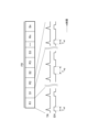
- FIG. 1 is a diagram showing a schematic configuration of a measurement system 100 according to a first embodiment of a distance measurement device of the present disclosure.
- 2 is a block diagram showing the functional configuration of a pixel 25 of the image sensor 1.
- FIG. 2 is a circuit diagram showing a circuit configuration of a pixel 25.
- FIG. 3 is a timing chart showing temporal changes in various signals for explaining the operation of the pixel 25.
- FIG. 5 is a timing chart showing time waveforms of an enable signal EN and a trigger signal TR generated by the pixel driver circuit 13 and the light source driver circuit 17.
- FIG. 7 is a graph showing histogram data created by the arithmetic circuit 7 for each pixel 25 over the frame period FR.
- FIG. 2 is a plan view showing the structure of a pixel 25A of the image sensor 1A.
- FIG. 2 is a timing chart illustrating the relationship between the timing of the gate pulse generated by the pixel driver circuit 13A and the arrival timing of the first light component L P1 and the second light component L P2 to the pixel 25.
- It is a diagram showing a schematic configuration of a measurement system 100B according to a third embodiment of the distance measurement device of the present disclosure.
- It is a figure showing the schematic structure of measurement system 100C concerning a 4th embodiment of the distance measurement device of this indication.
- It is a diagram showing a schematic configuration of a measurement system 100D according to a fifth embodiment of the distance measurement device of the present disclosure.
- the measurement system 100 shown in FIG. 1 detects the distance to the target object Sa two-dimensionally using the direct TOF (Time Of Flight) method, and uses the detection results to create a two-dimensional distance image or a three-dimensional Used to generate original CAD data.
- This measurement system 100 includes an image sensor (imaging device) 1, a light source 3 that emits pulsed light, an optical system (optical system) 5 that guides the pulsed light to the object Sa and the image sensor 1, and a distance information It is configured to include an arithmetic circuit (arithmetic processing circuit) 7 that performs calculations and a delay adjustment circuit 9.
- the light source 3 is a device that generates pulsed light LP that is irradiated onto the object Sa in order to perform distance measurement using the TOF method.
- the light source 3 is constituted by, for example, a semiconductor light emitting element such as a light emitting diode or a laser diode, and a drive circuit that drives the semiconductor light emitting element.
- a semiconductor light emitting element such as a light emitting diode or a laser diode
- a drive circuit that drives the semiconductor light emitting element.
- an element that generates light in a wavelength region such as a near-infrared region or a visible light region can be used.
- This light source 3 is configured to be able to emit pulsed light with a pulse width of 100 psec, for example. Note that the pulse width of the light emitted by the light source 3 is not limited to the above value, and can be set to various values.
- the image sensor 1 includes a light receiving surface 11, a pixel driver circuit 13, and a light source driver circuit (light source control circuit) 17, and these circuits are arranged on the same semiconductor chip or three-dimensionally stacked. It is integrated and configured on a chip. Note that although the arithmetic circuit 7 is configured on a circuit outside the image sensor 1, it may be integrated on the same semiconductor chip together with the image sensor 1.
- the light receiving surface 11 has a plurality of pixels 25 arranged two-dimensionally. Specifically, the light-receiving surface 11 is composed of a plurality of pixels 25 arranged in a two-dimensional matrix in N V rows and N H columns (N V and N H are integers of 2 or more), and forms a rectangular imaging area. Configure. A control signal for controlling the detection operation of the pixels 25 is applied from the pixel driver circuit 13 to each of these pixels 25 .
- the pixel driver circuit 13 generates a plurality of enable signals (control signals) for enabling (controlling) the pulsed light detection operation in each pixel 25 of the light receiving surface 11 based on the clock pulse CL input from the outside of the image sensor 1. ) generate and output EN.
- the pixel driver circuit 13 repeatedly generates a plurality of enable signals EN common to all pixels 25 as pulse-like voltage signals within a periodic frame period.
- the pulse width of the enable signal EN is set to such a time width that the pixel 25 can be controlled to detect photons.
- the pixel driver circuit 13 generates a common enable signal EN for each column of pixels 25 on the light-receiving surface 11, and applies the enable signal EN to each column of pixels 25.
- the light source driver circuit 17 generates a trigger signal TR that controls the irradiation (generation) timing of the pulsed light LP by the light source 3 based on the clock pulse CL input from the outside, and supplies the trigger signal TR to the light source 3. do.
- the light source driver circuit 17 repeatedly generates the trigger signal TR, which is a pulsed voltage signal synchronized with the plurality of enable signals EN, within the periodic frame period described above. Further, the light source driver circuit 17 supplies the trigger signal TR to the light source 3 and also to the pixels 25 on the light receiving surface 11 in order to control the detection operation of the pixels 25.
- the delay adjustment circuit 9 is electrically connected between the light source driver circuit 17 of the image sensor 1 and the light source 3. This delay adjustment circuit 9 causes a delay in the trigger signal TR output from the image sensor 1, and variably adjusts the time width of this delay.
- the delay adjustment circuit 9 is provided to adjust the emission timing of the pulsed light LP in response to signal delays of the enable signal EN and the trigger signal TR occurring within the image sensor 1.
- This delay adjustment circuit 9 may be integrated within the semiconductor chip constituting the image sensor 1, or may be integrated into a circuit outside the semiconductor chip.
- Optical system 5 includes a beam splitter 19, an optical waveguide 21, and lenses 23 and 27.
- the beam splitter 19 splits the pulsed light L P emitted from the light source 3 into a first light component L P1 that is incident on the object Sa and a second light component L P1 that is directly incident on the light receiving surface 11 without passing through the object Sa.
- This is a light splitting element that splits the light into light components L and P2 .
- the beam splitter 19 is, for example, a half mirror having a predetermined splitting ratio (reflectance, transmittance).
- the lens 23 is a lens that sets the irradiation range of the first light component L P1 divided by the beam splitter 19 to the range where the object Sa exists.
- the lens 27 is a lens that condenses the first light component L P1 reflected and returned by the object Sa so that it enters at least some of the pixels 25 on the light receiving surface 11 .
- the optical waveguide 21 directs the second light component L P2 split by the beam splitter 19 to at least some of the pixels 25 on the light receiving surface 11, into which the first light component L P1 is incident.
- This is an optical element that guides light to the same plurality of pixels 25 as the pixel 25.
- an optical fiber is used as the optical waveguide 21.
- an optical isolator or the like may be used to propagate light in one direction.
- FIG. 2 is a block diagram showing the functional configuration of the pixel 25
- FIG. 3 is a circuit diagram showing the circuit configuration of the pixel 25.
- the pixel 25 includes a SPAD (Single Photon Avalanche Diode) 29, which is a photoelectric conversion element, a waveform shaper 31, and a TDC (Time to Digital Converter) 33.
- the SPAD 29 is a light receiving element that photoelectrically converts incident photons to generate a pulse voltage (electrical signal).
- the waveform shaper 31 is electrically connected after the SPAD 29 and amplifies and shapes the pulse voltage generated by the SPAD 29 to generate an amplified pulse voltage (electrical signal).
- the TDC 33 counts the time from the timing of the trigger signal TR input from the light source driver circuit 17 to the timing of the amplified pulse voltage generated by the waveform shaper 31, and converts the count value into a digital signal (electrical signal) DC.
- the pixel 25 having such a configuration can detect the arrival timing of the first light component L P1 and the second light component L P2 that are incident on the pixel 25 based on the irradiation timing of the light source 3. The result can be output as a digital signal (electrical signal) DC .
- the pixel 25 is configured such that a plurality of enable signals EN are input from the pixel driver circuit 13 to the SPAD 29.
- the SPAD 29 detects incident photons and generates a pulse voltage during a period when the input enable signal EN is on, and does not generate a pulse voltage (photons) during a period when the input enable signal EN is off. configured so as not to detect
- the pixel 25 only needs to be configured so that the detection operation of the first light component L P1 and the second light component L P2 is enabled by the enable signal EN, and the pixel 25 is configured so that the detection operation of the first light component L P1 and the second light component L P2 is enabled by the enable signal EN.
- the operation may be configured to be enabled by an enable signal EN.
- the configuration shown in FIG. 3 can be adopted.
- the SPAD 29 is constituted by an avalanche diode.
- a cathode potential V DD_SPAD set higher than the anode potential is applied to the cathode of the SPAD 29 via a switching element 35 which is an N-channel MOS transistor.
- the cathode of the SPAD 29 is connected to the input of the waveform shaper 31 via a switching element 37 that is an N-channel MOS transistor.
- the switching element 35 is configured to switch in response to an enable signal EN
- the switching element 37 is configured to switch in response to an enable signal ENd generated in synchronization with the enable signal.
- the waveform shaper 31 is configured as an inverting amplifier that inverts and amplifies the cathode voltage of the SPAD 29.
- FIG. 4 is a timing chart showing temporal changes in various signals for explaining the operation of the pixel 25.
- the TDC 33 starts counting time at the timing when the trigger signal TR is turned on.
- the enable signal EN becomes a high state
- the enable signal ENd is delayed and becomes a high state in synchronization with it
- the switching elements 35 and 37 are made conductive
- the cathode potential VK of the SPAD 29 is set high to the potential VDD_SPAD . .
- the cathode potential VK decreases due to the avalanche-multiplied photocurrent, and the cathode potential VK is input to the waveform shaper 31 via the switching element 37, causing the waveform shaper to 31 outputs an amplified pulse voltage VP whose potential increases in a pulsed manner.
- the TDC 33 stops counting at the voltage rise timing of this amplified pulse voltage VP , measures the time difference T tot between the timing of the trigger signal TR and the timing of incidence of the photon, and outputs it as a digital signal DC .
- FIG. 5 is a timing chart showing the time waveforms of the enable signal EN and trigger signal TR generated by the pixel driver circuit 13 and the light source driver circuit 17.
- the pixel driver circuit 13 and the light source driver circuit 17 have a function of generating an enable signal EN and a trigger signal TR at a predetermined timing for each frame period FR that is repeated at a predetermined cycle. That is, the light source driver circuit 17 determines that the timing of generation of the pulsed light LP in the light source 3 is determined by sub-frame periods R1, S1, R2, S2, R3, S3,...Rn, which are temporally sequentially divided frame periods FR. At Sn (n is an integer of 2 or more), the trigger signal TR is generated at a repeating timing of a predetermined period.
- the pixel driver circuit 13 sets the on-period of the enable signal EN so as to overlap the period Tref including the arrival timing of the second light component LP2 with respect to the generation timing of the pulsed light LP .
- (period 2) R1, R2, R3,...Rn, and the on-period of the enable signal EN is set so as to overlap with the period Tsig that includes the arrival timing of the first optical component L P1 with respect to the generation timing of the pulsed light L P
- the enable signal EN is generated so that the subframe periods (first periods) S1, S2, S3, . . . Sn are set separately in time.
- the detection operation of the pixel 25 is enabled at the arrival timing of the second light component L P2 , and the second light component L P2 is activated.
- the arrival timing of the light component L P2 is detected, and in subframe periods (first periods) S1, S2, S3, ... Sn, the detection operation of the pixel 25 is enabled at the arrival timing of the first light component L P1 .
- the arrival timing of the first light component L P1 is detected.
- the pixel driver circuit 13 sets the enable signal EN so that the subframe periods R1, R2, R3, ...Rn and the subframe periods S1, S2, S3, ...Sn are alternately and repeatedly set. generate.
- the arithmetic circuit 7 determines the distance corresponding to the flight time of the pulsed light LP to the object Sa based on the digital signal DC output from each of the plurality of pixels 25 during the frame period FR. Information is generated for each plurality of pixels. That is, the arithmetic circuit 7 calculates histogram data obtained by summing up the frequencies of count values indicated by the digital signals DC for the plurality of digital signals DC repeatedly output from each of the plurality of pixels 25 during the frame period FR. create.
- FIG. 6 is a graph showing histogram data created by the arithmetic circuit 7 for each pixel 25 over the frame period FR.
- a distribution DT 1 corresponding to the arrival timing of the first light component L P1 and a distribution DT 2 corresponding to the arrival timing of the second light component L P2 appear.
- the arithmetic circuit 7 calculates a representative value for the distribution DT2 with the smaller count value, and based on the representative value, corresponds to the flight time of the second light component L P2 .
- the arithmetic circuit 7 calculates a representative value for the distribution DT1 with the larger count value, and based on the representative value, calculates time information TOF sig corresponding to the flight time of the first light component L P1 . get.
- the arithmetic circuit 7 may calculate an average value as a representative value in the distributions DT 1 and DT 2 , or may calculate another representative value such as a median value. Furthermore, the arithmetic circuit 7 generates distance information by taking the difference between the time information TOF sig and the time information TOF ref acquired for each pixel 25. The arithmetic circuit 7 finally generates and outputs a two-dimensional distance image or three-dimensional CAD data based on the distance information of all pixels 25 calculated for the frame period FR.
- the arithmetic circuit 7 creates one histogram data based on the digital signal DC detected during the sub-frame periods R1, R2, R3,...Rn within one frame period FR, and applies the histogram data to the histogram data. It is also possible to acquire the time information TOF ref for the distribution DT 2 corresponding to the arrival timing of the appearing second light component L P2 . Further, the arithmetic circuit 7 creates another histogram data based on the digital signal DC detected during the sub-frame periods S1, S2, S3,...Sn within one frame period FR, and uses the histogram data as It is also possible to obtain the time information TOF sig for the distribution DT 1 corresponding to the arrival timing of the first light component L P1 that appears.
- the distance measuring method of this embodiment includes the following steps.
- the light source driver circuit 17 controls the light source 3 to repeatedly generate pulsed light LP within the frame period FR (light source control step).
- the pulsed light L P generated from the light source 3 is divided into a first light component L P1 and a second light component L P2 by an optical system 5
- the first light component L P1 is divided into a first light component L P1 and a second light component L P2 .
- the second light component L P2 is directly guided toward the pixel 25 without passing through the object Sa (light splitting step).
- the pixel driver circuit 13 controls the enable timing so that the repetition timing of a predetermined period is reached in the sub-frame periods R1, S1, R2, S2, R3, S3, ... Rn, Sn that temporally divide the frame period FR.
- a signal EN is generated and the enable signal EN is applied to the plurality of pixels 25 (signal application step).
- the arithmetic circuit 7 generates histogram data based on the digital signal DC output for each of the plurality of pixels 25 corresponding to the frame period FR, and uses the histogram data to generate two time information TOF sig and TOF. A ref is obtained.
- Distance information is then generated by the arithmetic circuit 7 by taking the difference between the two time information TOF sig and TOF ref for each pixel, and two-dimensional information is generated based on the distance information of all pixels 25 calculated for the frame period FR.
- a distance image or three-dimensional CAD data is generated and output (computation processing step).
- the first light component L P1 which is the reflected light generated from the object Sa in response to the pulsed light L P from the light source 3
- the second light component L P2 of the pulsed light L P directly enters the plurality of pixels 25 , and in each of the plurality of pixels 25 operated by the enable signal EN applied from the pixel driver circuit 13 . Accordingly, a plurality of digital signals DC corresponding to the arrival timing of the first optical component L P1 and the arrival timing of the second optical component L P2 are output.
- a signal is generated corresponding to the arrival timing of each of the first light component L P1 and the second light component L P2 .
- the first time information TOF sig and the second time information TOF ref are calculated, and distance information corresponding to the flight time of the light to the object Sa is generated by taking the difference between the two time information TOF sig and TOF ref . be done.
- distance information can be obtained without spatially separating the pulsed light LP on the plurality of pixels 25.
- clock jitter occurs in the trigger signal TR given to the light source 3 from the light source driver circuit 17 and the delay adjustment circuit 9, and in the trigger signal TR given from the light source driver circuit 17 to the light receiving surface 11. Fluctuations in distance calculation values can be removed. That is, the clock jitter is caused by fluctuations ⁇ LM occurring in the trigger receiving circuit in the light source 3 and the driving circuit of the light emitting element such as a laser diode, fluctuations ⁇ DLC in the delay adjustment circuit 9 , and fluctuations ⁇ DLC in the light source driver circuit 17 in the image sensor 1 .
- the main cause is the fluctuation ⁇ TRIG .
- clock jitter with 1/f fluctuation cannot be reduced even by using frame averaging, which averages distance information between multiple frame periods FR to obtain the final distance, so the measurement accuracy of conventional distance measuring devices cannot be reduced. tends to be speed-limited by clock jitter.
- the change in the time information TOF ref calculated by detecting the second light component L P2 is caused by clock jitter because the optical path length of the second light component L P2 is fixed. It matches the fluctuation component given by . Therefore, by taking the difference between the two time information TOF sig and TOF ref , the clock jitter component in the common part can be removed, and the distance resolution can be improved to the theoretical limit determined only by the shot noise in the pixel.
- the light source driver circuit 17 controls the generation timing of the pulsed light LP within the frame period FR so that the timing is repeated, and the pixel driver circuit 13 controls the generation of the pulsed light LP .
- Sub-frame periods S1, S2, S3,...Sn in which the first light component L P1 is detected with respect to the timing, and sub-frame periods in which the second light component L P2 is detected in relation to the generation timing of the pulsed light L P R1, R2, R3, . . . Rn are set to be divided in time and repeated alternately.
- each of the plurality of pixels 25 alternately detects the arrival timing of the first light component L P1 and detects the arrival timing of the second light component L P2 in a temporally divided manner.
- the arithmetic circuit 7 of this embodiment calculates the first time information TOF sig based on the digital signal DC detected in the subframe periods S1, S2, S3,...Sn, and calculates the first time information TOF sig in the subframe periods R1, R2. , R3 , .
- the arithmetic circuit 7 of this embodiment calculates the first time information TOF sig based on the digital signal DC detected in the subframe periods S1, S2, S3,...Sn, and calculates the first time information TOF sig in the subframe periods R1, R2. , R3 , .
- each of the plurality of pixels 25 in this embodiment includes a photoelectric conversion element and a TDC (converter). According to such a configuration, it is possible to output digital signals D C that detect the arrival timings of the first and second light components L P1 and L P2 from the plurality of pixels 25, and these digital signals D C can be outputted. Through electrical processing, jitter components in distance information can be removed.
- the plurality of pixels 25 in this embodiment are configured such that the pulsed light detection operation can be enabled by an enable signal EN applied from the pixel driver circuit 13.
- the detection of the arrival timing of the first light component L P1 and the detection of the arrival timing of the second light component L P2 can be operated temporally separately for the plurality of pixels 25. It becomes easier. As a result, highly accurate distance information with reduced jitter effects can be generated without requiring a complicated control circuit.
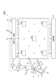
- the measurement system 100A shown in FIG. 7 two-dimensionally detects the distance to the target object Sa using the indirect TOF method, and compared to the measurement system 100 according to the first embodiment, the image sensor 1A
- the configuration and the function of the arithmetic circuit 7A are different.
- only the physical and functional configurations of the measurement system 100A that are different from the measurement system 100 will be described.
- a gate pulse (control pulse) that controls the pulsed light detection operation of the plurality of pixels 25A is applied from the pixel driver circuit 13A to each of the plurality of pixels 25A arranged on the light receiving surface 11A of the image sensor 1A.
- the pixel driver circuit 13A generates and outputs a plurality of gate pulses for controlling the timing of exposure (charge transfer) and charge discharge in each pixel 25A of the light receiving surface 11A based on the clock pulse CL.
- the pixel driver circuit 13A generates four gate pulses D G1 , D G2 , D G3 , and D G4 .
- the pixel driver circuit 13A similarly to the first embodiment, the pixel driver circuit 13A generates four gate pulses D G1 , D G2 at four types of predetermined delay times synchronized with the trigger signal TR within the frame period FR. , D G3 , and D G4 are repeatedly generated. Then, the pixel driver circuit 13A applies the four generated gate pulses D G1 , D G2 , D G3 , and D G4 to the corresponding control electrodes of all the pixels 25A.
- FIG. 8 is a plan view showing the structure of each of the plurality of pixels 25A.
- a photoelectric conversion region 41 that converts pulsed light incident at the center into electric charges is provided, and the four corners of the pixel 25A around the photoelectric conversion region 41 are spaced apart from each other and close to the photoelectric conversion region 41.
- Four charge readout regions 43 1 to 43 4 are arranged.
- a charge discharge region for discharging the pixel from the photoelectric conversion region 41 is also arranged in the pixel 25A (not shown).
- control electrodes G1 to G4 are provided on both sides of the charge transfer path 45 between the photoelectric conversion region 41 and each of the charge readout regions 43 1 to 43 4 , and a charge discharge region is provided from the photoelectric conversion region 41 to the charge discharge region.
- a control electrode (not shown) is provided on the charge transfer path between the two.
- These four pairs of control electrodes G1 to G4 are connected to each other via the charge transfer path 45 from the photoelectric conversion region 41 when gate pulses D G1 , D G2 , D G3 , and D G4 are applied from the pixel driver circuit 13A. It functions as a potential forming means for forming a potential that transfers charges toward each of the charge readout regions 43 1 to 43 4 .
- the pixel 25A also includes a circuit (not shown) that reads out a charge signal (electrical signal) corresponding to the amount of accumulated charge from each of the charge readout regions 43 1 to 43 4 .
- the pixels 25A accumulate charge in the charge readout regions 43 1 to 43 4 at a predetermined timing such as the end of the frame period FR in accordance with a control signal given from a control circuit (not shown) in the image sensor 1A.
- a charge signal having a potential corresponding to the amount of charge thus obtained is outputted to the arithmetic circuit 7.
- the pixel 25A resets the charges accumulated in the charge readout regions 43 1 to 43 4 at the same time as outputting the charge signal.
- FIG. 9 shows the timing of the gate pulses D G1 , D G2 , D G3 , and D G4 generated by the pixel driver circuit 13A, and the arrival of the first light component L P1 and the second light component L P2 to the pixel 25. It is a timing chart explaining the relationship with timing.
- the pulsed light L P is irradiated from the light source 3 to the object Sa at a timing based on the clock pulse CL inputted from the outside, the first light component L P1 reflected by the object Sa, The directly incident second light component L P2 enters each pixel 25A of the image sensor 1A, and at the timing corresponding to the first light component L P1 and the second light component L P2 , the photoelectric current of each pixel 25A is generated.
- a photocurrent I PH is generated in the conversion region 41 .
- the pixel driver circuit 13A applies gate pulses D G1 and D G2 to each of the control electrodes G1 and G2 of each pixel 25A based on the irradiation timing of the pulsed light LP (timing of the trigger signal TR ) .
- the timings of the on-periods are set in advance so as to straddle the timing of generation of the photocurrent IPH by the second light component L P2 so as not to overlap with each other. Thereby, charges generated by the photocurrent I PH due to the second light component L P2 are distributed to the charge readout regions 43 1 and 43 2 of each pixel 25 .
- the pixel driver circuit 13A also controls the gate pulses D G3 and D G4 applied to the control electrodes G3 and G4 of each pixel 25A based on the irradiation timing of the pulsed light LP (timing of the trigger signal TR).
- the timing of the on-period is set in advance so as to span the generation timing of the photocurrent IPH by the first light component L P1 so as not to overlap with each other. Thereby, charges generated by the photocurrent I PH caused by the first light component L P1 are distributed to the charge readout regions 43 3 and 43 4 of each pixel 25 .
- the arithmetic circuit 7A selects the charge readout area 43 1 based on a set of charge signals corresponding to the amount of charge accumulated in the charge readout area 43 1 , 43 2 among the plurality of charge signals output from each pixel 25A . , 43 2 , the second time information TOF ref is calculated. Further, the arithmetic circuit 7A calculates the charge readout area based on a set of charge signals corresponding to the amount of charge accumulated in the charge readout areas 43 3 and 43 4 among the plurality of charge signals output from each pixel 25A.
- the first time information TOF sig is calculated by calculating the ratio of the amount of charge distributed to 43 3 and 43 4 .
- pulsed light is emitted at timings corresponding to the gate pulses D G1 , D G2 , D G3 , and D G4 under the control of the pixel driver circuit 13A.
- Charges converted from are accumulated in a plurality of charge readout regions 43 1 , 43 2 , 43 3 , 43 4 , and in the arithmetic circuit 7A, charges converted from the plurality of charge readout regions 43 1 , 43 2 , output from each pixel 25A are stored.
- First time information TOF sig and second time information TOF ref are calculated using a plurality of charge signals corresponding to the charges of 43 3 and 43 4 , and distance information is generated by taking the difference between them. . This makes it possible to generate highly accurate distance information with reduced effects of jitter.
- the arithmetic circuit 7A calculates first time information TOF sig based on a set of charge signals among the plurality of charge signals output from each pixel 25A, and The second time information TOF ref is calculated based on the set of .
- the time information TOF sig and TOF ref can be calculated based on the difference in the amount of charge accumulated at different timings in one set of charge readout regions in the pixel 25A, and the time information TOF sig and TOF ref can be calculated based on the time information. Highly accurate distance information can be generated.
- the detection operation of the plurality of pixels 25 may be continuously enabled without intermittently enabling the detection operation of the plurality of pixels 25 by the enable signal EN. good.
- the pixel 25 does not need to have an enabling function using the enable signal EN.
- the division ratio of the beam splitter 19 of the optical system 5 is set in advance so that two peak distributions appear in the histogram data created by the arithmetic circuit 7. According to such a modification, the configuration of the image sensor 1 can be simplified.
- each pixel 25A may have a configuration in which less than four sets of charge readout regions and control electrodes are provided.
- the pixel 25A may have two sets of charge readout regions and control electrodes.
- the pixel driver circuit 13A controls the phase of the gate pulse for each column of the pixels 25A in the sub-frame periods R1, S1, R2, S2, R3, S3,...Rn, Sn that temporally divide the frame period FR in order.
- the timing of the gate pulse is set to correspond to the arrival timing of the second light component L P2 in the subframe periods R1, R2, R3, ..., Rn
- the timing of the gate pulse is The timing of the gate pulse may be set to correspond to the arrival timing of the first optical component L P1 during the periods S1, S2, S3, . . . , Sn.
- the arithmetic circuit 7A calculates the second time information TOF ref based on a set of charge signals detected in the subframe periods R1, R2, R3, ..., Rn, and calculates the second time information TOF ref in the subframe periods S1, S2.
- S3, . . . , Sn can be used to calculate the first time information TOF sig , and highly accurate distance information can be generated based on the difference between the time information.
- the pixel driver circuit 13A sets the timing of the gate pulse for each row of the pixels 25A in addition to setting the timing of the gate pulse for each column of the pixels 25A.
- the acquisition of the first light component L P1 and the second light component L P2 may be switched over in time.
- the distance measuring device is not limited to one having a plurality of pixels, but can also be applied to a sensor having a single pixel.
- the configuration of an embodiment of a distance measuring device including a single pixel will be described below.
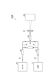
- FIG. 10 shows the configuration of a measurement system 100B according to the third embodiment.
- the measurement system 100B includes a sensor 1B composed of a single pixel, a light source 3, a waveguide 51 that optically connects the sensor 1B and the light source 3, optical elements A3, A4, A5, and A6, and a light projector. and a lens A7 with an integrated light receiving section.
- the pulsed light L P from the light source 3 is branched into a first light component L P1 and a second light component L P2 by an optical element A3 such as a coupler.
- the light emitting path to the object Sa and the light receiving path to the sensor 1B are combined by an optical element A6 such as a coupler, and the first light component L P1 is emitted to the object Sa using the lens A7.
- the reflected light of the first light component L P1 is received by using the light beam.
- the received first light component L P1 is combined with the second light component L P2 by an optical element A5 such as a coupler, and then input to the sensor 1B.
- the propagation direction of light may be limited by using a circulator or the like as the optical element A6.
- an isolator may be provided between the optical elements A3 to A6 to suppress return light.
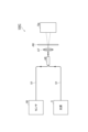
- FIG. 11 shows the configuration of a measurement system 100C according to the fourth embodiment
- FIG. 12 shows the configuration of a measurement system 100D according to the fifth embodiment
- the second light component L P2 is not formed by a waveguide but by an optical element A8 such as a cover glass disposed between the lens A7 and the object Sa. It may also be generated as return light by, for example.
- a histogram as shown in FIG. 6 is created based on the first light component L P1 reflected by the object Sa and the second light component L P2 generated as return light. is generated, and differential processing is performed based on the histogram.
- the measurement system 100D is configured to measure the distance of a transparent or translucent object, such as a liquid level, as the object Sa.
- an optical element A8 such as a cover glass is placed away from the object Sa on the opposite side of the lens A7 in order to generate return light based on the light that has passed through the object Sa.
- a histogram is generated based on the first light component L P1 reflected by the object Sa and the second light component L P2 generated as return light.
- the light source control circuit controls the generation timing to be a repeating timing, and the driver circuit controls a first period in which the first light component is detected with respect to the generation timing; It is preferable to apply the control signal so that the second period for detecting the second light component is set to be temporally separated from the generation timing. If such a configuration is adopted, the pixel is controlled to temporally separate the detection of the arrival timing of the first light component and the detection of the arrival timing of the second light component, and the difference between these detection results is calculated. This makes it possible to generate highly accurate distance information with reduced effects of jitter.
- the driver circuit apply a control signal so as to alternately and repeatedly set the first period and the second period.
- the pixel is controlled to alternately detect the arrival timing of the first light component and the arrival timing of the second light component, and by taking the difference between these detection results, the jitter is eliminated. It is possible to generate highly accurate distance information in which the influence of
- the arithmetic processing circuit calculates first time information based on the electrical signal detected in the first period, and calculates second time information based on the electrical signal detected in the second period. , is also preferable. According to such a configuration, by taking the difference between the first and second time information, it is possible to generate highly accurate distance information in which the influence of jitter is reduced.
- the pixel includes a photoelectric conversion element that photoelectrically converts pulsed light and a converter that converts the timing of the photoelectrically converted pulsed light into a digital signal, and outputs the digital signal as an electrical signal.
- a photoelectric conversion element that photoelectrically converts pulsed light
- a converter that converts the timing of the photoelectrically converted pulsed light into a digital signal
- the digital signal as an electrical signal.
- the light source control circuit controls the generation timing to be a repeating timing
- the driver circuit controls a first period in which the operation of the pixel is enabled at the arrival timing of the first light component with respect to the generation timing
- the control signal so that the second period for validating the pixel operation is set to be temporally separate from the arrival timing of the second light component relative to the generation timing.
- the pixel is controlled to temporally separate the detection of the arrival timing of the first light component and the detection of the arrival timing of the second light component, and the difference between the digital signals that are the results of these detections is controlled.
- the pixel corresponds to a photoelectric conversion region that converts pulsed light into charges, a plurality of charge readout regions provided close to the photoelectric conversion region and separated from each other, and a photoelectric conversion region and a plurality of charge readout regions. They each have a plurality of control electrodes for applying a plurality of control pulses for charge transfer between the photoelectric conversion region and the plurality of charge readout regions, and have a plurality of control electrodes for applying a plurality of control pulses for charge transfer between the photoelectric conversion region and the plurality of charge readout regions.
- the driver circuit applies a plurality of control pulses to the plurality of control electrodes, respectively, and the arithmetic processing circuit outputs the plurality of charge signals output from the pixels as electrical signals.
- the first time information based on the charge signals and calculate the second time information based on the plurality of charge signals.
- the charges converted from the pulsed light are accumulated in a plurality of charge readout areas at the timing corresponding to the control pulse, and the arithmetic processing circuit stores the charges output from the pixel.
- First and second time information are calculated using a plurality of charge signals corresponding to the charges in the readout region, and distance information is generated by taking the difference between them. This makes it possible to generate highly accurate distance information with reduced effects of jitter.
- the arithmetic processing circuit calculates first time information based on a set of charge signals among the plurality of charge signals, and calculates second time information based on a different set of charge signals among the plurality of charge signals. It is also preferable to calculate. According to this configuration, time information can be calculated based on the difference in the amount of charge accumulated at different timings in one set of charge readout areas, and highly accurate distance information can be generated based on the time information. .
- the light source control circuit controls the generation timing to be a repeating timing
- the driver circuit sets the timing of the plurality of control pulses to correspond to the arrival timing of the first light component with respect to the generation timing.
- the first period and the second period in which the timing of the plurality of control pulses is set to correspond to the arrival timing of the second light component with respect to the generation timing are set separately in time, and the arithmetic processing circuit
- the first time information may be calculated based on the plurality of charge signals detected in the first period
- the second time information may be calculated based on the plurality of charge signals detected in the second period. preferable.
- the pixel is controlled to temporally separate the detection of the arrival timing of the first light component and the detection of the arrival timing of the second light component, and the plurality of detection results are By taking the difference between the time information calculated based on the charge signal, it is possible to generate highly accurate distance information in which the influence of jitter is reduced.
- the distance measuring device of the present disclosure includes [1] a light source that generates pulsed light, a light source control circuit that controls the generation timing of the pulsed light, detects the arrival timing of the pulsed light, and generates an electrical signal corresponding to the arrival timing. Divide the output pixel and the pulsed light generated from the light source into a first light component that reflects off the object and enters the pixel, and a second light component that enters the pixel without passing through the object.
- An optical system, a driver circuit that applies a control signal to the pixel to control the detection operation of the pixel, and a calculation that generates distance information corresponding to the flight time of light to the target object based on the electrical signal output by the pixel.
- the arithmetic processing circuit is configured to generate first time information corresponding to the arrival timing of the first light component and arrival timing of the second light component based on the plurality of electrical signals output from the pixels. and second time information corresponding to the timing, and generates distance information by calculating the difference between the first time information and the second time information.
- the distance measuring device of the present disclosure has the following features: [2] “The light source control circuit controls the generation timing to be a repeating timing, and the driver circuit controls the first light component to detect the first light component with respect to the generation timing. and the second period for detecting the second light component with respect to the generation timing, which applies a control signal so as to set the period separately in time, and the distance measuring device according to [1] above. There may be.
- the distance measuring device of the present disclosure provides the distance measuring device according to [3] “The driver circuit applies the control signal so as to alternately and repeatedly set the first period and the second period. It may also be a “device”.
- the distance measuring device of the present disclosure includes [4] "The arithmetic processing circuit calculates first time information based on the electrical signal detected in the first period, and calculates the first time information based on the electrical signal detected in the second period.
- the distance measuring device according to [2] or [3] above, which calculates the second time information based on the distance measuring device.
- the distance measuring device of the present disclosure includes [5] "The pixel includes a photoelectric conversion element that photoelectrically converts pulsed light and a converter that converts the timing of the photoelectrically converted pulsed light into a digital signal, and the pixel converts the digital signal into an electrical signal.
- the distance measuring device according to any one of [1] to [4] above, which outputs a signal as a signal.
- the distance measuring device of the present disclosure has the following features: [6] "The light source control circuit controls the generation timing to be a repeating timing, and the driver circuit controls the operation of the pixel at the arrival timing of the first light component with respect to the generation timing. Applying a control signal so as to set a first period of activation and a second period of activation of the pixel at the arrival timing of the second light component with respect to the generation timing to be separated in time; The distance measuring device according to any one of [1] to [5] above may be used.
- the distance measuring device of the present disclosure includes [7] “The pixel includes a photoelectric conversion region that converts pulsed light into charges, a plurality of charge readout regions provided close to the photoelectric conversion region and spaced apart from each other, and a photoelectric conversion region.
- the driver circuit outputs a plurality of charge signals corresponding to the charges accumulated in the plurality of charge readout regions as electrical signals, the driver circuit applies a plurality of control pulses to the plurality of control electrodes, and the arithmetic processing circuit: Any of the above [1] to [4], wherein the first time information is calculated based on a plurality of charge signals output from a pixel, and the second time information is calculated based on the plurality of charge signals.
- the distance measuring device described in the above may be used.
- the distance measuring device of the present disclosure includes [8] "The arithmetic processing circuit calculates first time information based on a set of charge signals among the plurality of charge signals, and calculates first time information based on a set of charge signals among the plurality of charge signals, and The distance measuring device according to [7] above may calculate the second time information based on the set of .
- the distance measuring device of the present disclosure has the following features: [9] “The light source control circuit controls the generation timing to be a repeating timing, and the driver circuit controls the generation timing to correspond to the arrival timing of the first light component with respect to the generation timing. A first period in which the timing of the plurality of control pulses is set and a second period in which the timing of the plurality of control pulses is set so as to correspond to the arrival timing of the second light component with respect to the generation timing are temporally divided.
- the arithmetic processing circuit calculates first time information based on the plurality of charge signals detected in the first period, and calculates the second time information based on the plurality of charge signals detected in the second period.
- the distance measuring device described in [7] or [8] above may be used.
Landscapes
- Engineering & Computer Science (AREA)
- Physics & Mathematics (AREA)
- General Physics & Mathematics (AREA)
- Radar, Positioning & Navigation (AREA)
- Remote Sensing (AREA)
- Computer Networks & Wireless Communication (AREA)
- Electromagnetism (AREA)
- Optical Radar Systems And Details Thereof (AREA)
Priority Applications (1)
| Application Number | Priority Date | Filing Date | Title |
|---|---|---|---|
| JP2024537722A JPWO2024024744A1 (https=) | 2022-07-28 | 2023-07-24 |
Applications Claiming Priority (2)
| Application Number | Priority Date | Filing Date | Title |
|---|---|---|---|
| JP2022120331 | 2022-07-28 | ||
| JP2022-120331 | 2022-07-28 |
Publications (1)
| Publication Number | Publication Date |
|---|---|
| WO2024024744A1 true WO2024024744A1 (ja) | 2024-02-01 |
Family
ID=89706628
Family Applications (1)
| Application Number | Title | Priority Date | Filing Date |
|---|---|---|---|
| PCT/JP2023/027058 Ceased WO2024024744A1 (ja) | 2022-07-28 | 2023-07-24 | 距離計測装置及び距離計測方法 |
Country Status (2)
| Country | Link |
|---|---|
| JP (1) | JPWO2024024744A1 (https=) |
| WO (1) | WO2024024744A1 (https=) |
Citations (4)
| Publication number | Priority date | Publication date | Assignee | Title |
|---|---|---|---|---|
| US20140071433A1 (en) * | 2011-03-17 | 2014-03-13 | Robert Bosch Gmbh | Measurement Device for Measuring a Distance between the Measurement Device and a Target Object using an Optical Measurement Beam |
| US20170366737A1 (en) * | 2016-06-15 | 2017-12-21 | Stmicroelectronics, Inc. | Glass detection with time of flight sensor |
| JP2019527830A (ja) * | 2016-08-11 | 2019-10-03 | クアルコム,インコーポレイテッド | 光学システムにおいて参照および戻された光ビームを測定するためのシステムおよび方法 |
| WO2021193532A1 (ja) * | 2020-03-23 | 2021-09-30 | 国立大学法人静岡大学 | 距離画像取得装置 |
-
2023
- 2023-07-24 JP JP2024537722A patent/JPWO2024024744A1/ja active Pending
- 2023-07-24 WO PCT/JP2023/027058 patent/WO2024024744A1/ja not_active Ceased
Patent Citations (4)
| Publication number | Priority date | Publication date | Assignee | Title |
|---|---|---|---|---|
| US20140071433A1 (en) * | 2011-03-17 | 2014-03-13 | Robert Bosch Gmbh | Measurement Device for Measuring a Distance between the Measurement Device and a Target Object using an Optical Measurement Beam |
| US20170366737A1 (en) * | 2016-06-15 | 2017-12-21 | Stmicroelectronics, Inc. | Glass detection with time of flight sensor |
| JP2019527830A (ja) * | 2016-08-11 | 2019-10-03 | クアルコム,インコーポレイテッド | 光学システムにおいて参照および戻された光ビームを測定するためのシステムおよび方法 |
| WO2021193532A1 (ja) * | 2020-03-23 | 2021-09-30 | 国立大学法人静岡大学 | 距離画像取得装置 |
Also Published As
| Publication number | Publication date |
|---|---|
| JPWO2024024744A1 (https=) | 2024-02-01 |
Similar Documents
| Publication | Publication Date | Title |
|---|---|---|
| US11140340B2 (en) | Single-chip RGB-D camera | |
| US8767189B2 (en) | Solid state imaging device and distance image measurement device | |
| TWI780462B (zh) | 距離影像攝像裝置及距離影像攝像方法 | |
| JP6741680B2 (ja) | 撮像装置、およびそれに用いられる固体撮像素子 | |
| US7436496B2 (en) | Distance image sensor | |
| JP5107440B2 (ja) | 三次元アクティブ画像処理デバイス | |
| CN112114328B (zh) | 飞时测距装置 | |
| JP7082404B2 (ja) | 距離計測装置 | |
| KR20170015941A (ko) | 측거 장치 | |
| JP2024041961A (ja) | 距離画像撮像装置、及び距離画像撮像方法 | |
| WO2025211035A1 (ja) | 測距装置 | |
| WO2024024744A1 (ja) | 距離計測装置及び距離計測方法 | |
| JP7739719B2 (ja) | 距離画像撮像装置、及び距離画像撮像方法 | |
| GB2620898A (en) | Light receiving device and distance measuring device | |
| CN113820725A (zh) | 一种执行飞行时间测量的系统、方法及电子设备 | |
| CN115136023A (zh) | 距离测定装置及距离测定方法 | |
| JP7604907B2 (ja) | 距離画像撮像装置、及び距離画像撮像方法 | |
| JP2023147558A (ja) | 距離画像撮像装置、及び距離画像撮像方法 | |
| US20250155558A1 (en) | Distance measuring device and distance measuring method | |
| JP7516146B2 (ja) | 光検出システム | |
| WO2021156446A1 (en) | A light pixel projection module | |
| JP2026010609A (ja) | 測距装置 | |
| JP2025089961A (ja) | 距離画像撮像装置、及び距離画像撮像方法 | |
| WO2023234253A1 (ja) | 距離画像撮像装置、及び距離画像撮像方法 | |
| CN120201275A (zh) | 距离图像摄像装置以及距离图像摄像方法 |
Legal Events
| Date | Code | Title | Description |
|---|---|---|---|
| 121 | Ep: the epo has been informed by wipo that ep was designated in this application |
Ref document number: 23846474 Country of ref document: EP Kind code of ref document: A1 |
|
| WWE | Wipo information: entry into national phase |
Ref document number: 2024537722 Country of ref document: JP |
|
| NENP | Non-entry into the national phase |
Ref country code: DE |
|
| 122 | Ep: pct application non-entry in european phase |
Ref document number: 23846474 Country of ref document: EP Kind code of ref document: A1 |