WO2024024744A1 - Distance measuring device and distance measuring method - Google Patents
Distance measuring device and distance measuring method Download PDFInfo
- Publication number
- WO2024024744A1 WO2024024744A1 PCT/JP2023/027058 JP2023027058W WO2024024744A1 WO 2024024744 A1 WO2024024744 A1 WO 2024024744A1 JP 2023027058 W JP2023027058 W JP 2023027058W WO 2024024744 A1 WO2024024744 A1 WO 2024024744A1
- Authority
- WO
- WIPO (PCT)
- Prior art keywords
- light
- pixel
- timing
- time information
- light component
- Prior art date
Links
- 238000000034 method Methods 0.000 title description 9
- 230000003287 optical effect Effects 0.000 claims abstract description 42
- 238000001514 detection method Methods 0.000 claims abstract description 31
- 238000012545 processing Methods 0.000 claims description 33
- 238000006243 chemical reaction Methods 0.000 claims description 28
- 238000012546 transfer Methods 0.000 claims description 9
- 238000000691 measurement method Methods 0.000 claims description 3
- 238000005259 measurement Methods 0.000 description 34
- 238000010586 diagram Methods 0.000 description 9
- 238000009826 distribution Methods 0.000 description 9
- 230000000694 effects Effects 0.000 description 8
- 230000004044 response Effects 0.000 description 6
- 239000004065 semiconductor Substances 0.000 description 6
- 238000003384 imaging method Methods 0.000 description 3
- 230000004913 activation Effects 0.000 description 2
- 239000006059 cover glass Substances 0.000 description 2
- 238000012986 modification Methods 0.000 description 2
- 230000004048 modification Effects 0.000 description 2
- 239000013307 optical fiber Substances 0.000 description 2
- 230000000737 periodic effect Effects 0.000 description 2
- 230000001360 synchronised effect Effects 0.000 description 2
- 230000002123 temporal effect Effects 0.000 description 2
- 238000002366 time-of-flight method Methods 0.000 description 2
- 238000012935 Averaging Methods 0.000 description 1
- 230000008859 change Effects 0.000 description 1
- 230000007423 decrease Effects 0.000 description 1
- 230000001934 delay Effects 0.000 description 1
- 230000003111 delayed effect Effects 0.000 description 1
- 238000007599 discharging Methods 0.000 description 1
- 230000007274 generation of a signal involved in cell-cell signaling Effects 0.000 description 1
- 239000004615 ingredient Substances 0.000 description 1
- 239000007788 liquid Substances 0.000 description 1
- 239000011159 matrix material Substances 0.000 description 1
- 238000002834 transmittance Methods 0.000 description 1
Images


Classifications
-
- G—PHYSICS
- G01—MEASURING; TESTING
- G01C—MEASURING DISTANCES, LEVELS OR BEARINGS; SURVEYING; NAVIGATION; GYROSCOPIC INSTRUMENTS; PHOTOGRAMMETRY OR VIDEOGRAMMETRY
- G01C3/00—Measuring distances in line of sight; Optical rangefinders
- G01C3/02—Details
- G01C3/06—Use of electric means to obtain final indication
-
- G—PHYSICS
- G01—MEASURING; TESTING
- G01S—RADIO DIRECTION-FINDING; RADIO NAVIGATION; DETERMINING DISTANCE OR VELOCITY BY USE OF RADIO WAVES; LOCATING OR PRESENCE-DETECTING BY USE OF THE REFLECTION OR RERADIATION OF RADIO WAVES; ANALOGOUS ARRANGEMENTS USING OTHER WAVES
- G01S7/00—Details of systems according to groups G01S13/00, G01S15/00, G01S17/00
- G01S7/48—Details of systems according to groups G01S13/00, G01S15/00, G01S17/00 of systems according to group G01S17/00
- G01S7/483—Details of pulse systems
- G01S7/486—Receivers
- G01S7/4865—Time delay measurement, e.g. time-of-flight measurement, time of arrival measurement or determining the exact position of a peak
Definitions
- the present invention relates to a distance measuring device and a distance measuring method that generate distance information for each pixel.
- Patent Document 1 Conventionally, devices have been used that generate image signals including distance information using the flight time of light (for example, see Patent Document 1 below).
- the device described in Patent Document 1 below irradiates a target object with pulsed light from a light source, and accumulates the charges generated in response within pixels in different periods set by control pulses.
- Distance information is obtained by reading electrical signals corresponding to each charge and calculating the distance for each pixel based on these electrical signals. Note that in the above device, when attempting to achieve a distance accuracy of over 100 ⁇ m, jitter in the driver circuit for applying control pulses to pixels becomes a problem.
- the light-receiving surface on which pixels are arranged two-dimensionally is divided into two, and the pulsed light reflected by the object is incident on one light-receiving surface, and the pulsed light is reflected from the reference surface on the other light-receiving surface. It is configured to reduce the influence of jitter on the distance calculation value by inputting the pulsed light and calculating a difference between the distance calculation values calculated based on the respective pulsed lights.
- the present invention has been made in view of the above problems, and provides a distance measuring device and a distance measuring method that are capable of generating highly accurate distance information in which the influence of jitter is reduced without complicating the optical system.
- the purpose is to provide
- a distance measuring device includes a light source that generates pulsed light, a light source control circuit that controls the generation timing of the pulsed light, and a light source that detects the arrival timing of the pulsed light and detects the arrival timing of the pulsed light.
- a pixel that outputs an electrical signal corresponding to the timing, a first light component that reflects pulsed light from a light source and enters the pixel, and a second light component that enters the pixel without passing through the object.
- An optical system that divides the light into two light components, a driver circuit that applies a control signal to the pixel that controls the detection operation of the pixel, and an electrical signal output by the pixel that corresponds to the flight time of the light to the target object.
- an arithmetic processing circuit that generates distance information based on the plurality of electrical signals output from the pixels, and the arithmetic processing circuit that generates first time information corresponding to the arrival timing of the first light component; second time information corresponding to the arrival timing of the second light component, and distance information is generated by calculating the difference between the first time information and the second time information.
- a distance measuring method includes a light source control step in which a light source control circuit controls the light source to generate pulsed light; and an optical system that directs the pulsed light generated from the light source toward the object.
- a light splitting step of dividing the light into a first light component that reflects and enters the pixel and a second light component that enters the pixel without passing through the object, and detecting the arrival timing of the pulsed light and detecting the arrival timing of the pulsed light.
- a signal application step in which the driver circuit applies a control signal to the pixel to control the detection operation of the pixel, and an arithmetic processing circuit applies the electric signal output by the pixel to the pixel that outputs the electric signal corresponding to the timing.
- the first time information corresponding to the arrival timing of the second light component and the second time information corresponding to the arrival timing of the second light component are calculated, and the difference between the first time information and the second time information is calculated.
- the first light component which is the reflected light generated from the object in response to the pulsed light from the light source, and the first light component that does not pass through the object.
- the second light component of the pulsed light that is directly incident on the pixel enters the pixel, and the pixel, which operates according to the control signal applied from the driver circuit, changes the arrival timing of the first light component and the second light component accordingly.
- a plurality of electrical signals corresponding to the arrival timing of the optical components are output.
- first and second time information corresponding to the respective arrival timings of the first and second light components are calculated using the plurality of electrical signals output from the pixels, and the two Distance information corresponding to the flight time of light to the target object is generated by taking the difference in time information.
- jitter components caused by driver circuits and light sources in distance information can be removed without spatially separating pulsed light on multiple pixels. can be deleted.
- highly accurate distance information with reduced jitter effects can be generated without complicating the optical system.
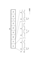
- FIG. 1 is a diagram showing a schematic configuration of a measurement system 100 according to a first embodiment of a distance measurement device of the present disclosure.
- 2 is a block diagram showing the functional configuration of a pixel 25 of the image sensor 1.
- FIG. 2 is a circuit diagram showing a circuit configuration of a pixel 25.
- FIG. 3 is a timing chart showing temporal changes in various signals for explaining the operation of the pixel 25.
- FIG. 5 is a timing chart showing time waveforms of an enable signal EN and a trigger signal TR generated by the pixel driver circuit 13 and the light source driver circuit 17.
- FIG. 7 is a graph showing histogram data created by the arithmetic circuit 7 for each pixel 25 over the frame period FR.
- FIG. 2 is a plan view showing the structure of a pixel 25A of the image sensor 1A.
- FIG. 2 is a timing chart illustrating the relationship between the timing of the gate pulse generated by the pixel driver circuit 13A and the arrival timing of the first light component L P1 and the second light component L P2 to the pixel 25.
- It is a diagram showing a schematic configuration of a measurement system 100B according to a third embodiment of the distance measurement device of the present disclosure.
- It is a figure showing the schematic structure of measurement system 100C concerning a 4th embodiment of the distance measurement device of this indication.
- It is a diagram showing a schematic configuration of a measurement system 100D according to a fifth embodiment of the distance measurement device of the present disclosure.
- the measurement system 100 shown in FIG. 1 detects the distance to the target object Sa two-dimensionally using the direct TOF (Time Of Flight) method, and uses the detection results to create a two-dimensional distance image or a three-dimensional Used to generate original CAD data.
- This measurement system 100 includes an image sensor (imaging device) 1, a light source 3 that emits pulsed light, an optical system (optical system) 5 that guides the pulsed light to the object Sa and the image sensor 1, and a distance information It is configured to include an arithmetic circuit (arithmetic processing circuit) 7 that performs calculations and a delay adjustment circuit 9.
- the light source 3 is a device that generates pulsed light LP that is irradiated onto the object Sa in order to perform distance measurement using the TOF method.
- the light source 3 is constituted by, for example, a semiconductor light emitting element such as a light emitting diode or a laser diode, and a drive circuit that drives the semiconductor light emitting element.
- a semiconductor light emitting element such as a light emitting diode or a laser diode
- a drive circuit that drives the semiconductor light emitting element.
- an element that generates light in a wavelength region such as a near-infrared region or a visible light region can be used.
- This light source 3 is configured to be able to emit pulsed light with a pulse width of 100 psec, for example. Note that the pulse width of the light emitted by the light source 3 is not limited to the above value, and can be set to various values.
- the image sensor 1 includes a light receiving surface 11, a pixel driver circuit 13, and a light source driver circuit (light source control circuit) 17, and these circuits are arranged on the same semiconductor chip or three-dimensionally stacked. It is integrated and configured on a chip. Note that although the arithmetic circuit 7 is configured on a circuit outside the image sensor 1, it may be integrated on the same semiconductor chip together with the image sensor 1.
- the light receiving surface 11 has a plurality of pixels 25 arranged two-dimensionally. Specifically, the light-receiving surface 11 is composed of a plurality of pixels 25 arranged in a two-dimensional matrix in N V rows and N H columns (N V and N H are integers of 2 or more), and forms a rectangular imaging area. Configure. A control signal for controlling the detection operation of the pixels 25 is applied from the pixel driver circuit 13 to each of these pixels 25 .
- the pixel driver circuit 13 generates a plurality of enable signals (control signals) for enabling (controlling) the pulsed light detection operation in each pixel 25 of the light receiving surface 11 based on the clock pulse CL input from the outside of the image sensor 1. ) generate and output EN.
- the pixel driver circuit 13 repeatedly generates a plurality of enable signals EN common to all pixels 25 as pulse-like voltage signals within a periodic frame period.
- the pulse width of the enable signal EN is set to such a time width that the pixel 25 can be controlled to detect photons.
- the pixel driver circuit 13 generates a common enable signal EN for each column of pixels 25 on the light-receiving surface 11, and applies the enable signal EN to each column of pixels 25.
- the light source driver circuit 17 generates a trigger signal TR that controls the irradiation (generation) timing of the pulsed light LP by the light source 3 based on the clock pulse CL input from the outside, and supplies the trigger signal TR to the light source 3. do.
- the light source driver circuit 17 repeatedly generates the trigger signal TR, which is a pulsed voltage signal synchronized with the plurality of enable signals EN, within the periodic frame period described above. Further, the light source driver circuit 17 supplies the trigger signal TR to the light source 3 and also to the pixels 25 on the light receiving surface 11 in order to control the detection operation of the pixels 25.
- the delay adjustment circuit 9 is electrically connected between the light source driver circuit 17 of the image sensor 1 and the light source 3. This delay adjustment circuit 9 causes a delay in the trigger signal TR output from the image sensor 1, and variably adjusts the time width of this delay.
- the delay adjustment circuit 9 is provided to adjust the emission timing of the pulsed light LP in response to signal delays of the enable signal EN and the trigger signal TR occurring within the image sensor 1.
- This delay adjustment circuit 9 may be integrated within the semiconductor chip constituting the image sensor 1, or may be integrated into a circuit outside the semiconductor chip.
- Optical system 5 includes a beam splitter 19, an optical waveguide 21, and lenses 23 and 27.
- the beam splitter 19 splits the pulsed light L P emitted from the light source 3 into a first light component L P1 that is incident on the object Sa and a second light component L P1 that is directly incident on the light receiving surface 11 without passing through the object Sa.
- This is a light splitting element that splits the light into light components L and P2 .
- the beam splitter 19 is, for example, a half mirror having a predetermined splitting ratio (reflectance, transmittance).
- the lens 23 is a lens that sets the irradiation range of the first light component L P1 divided by the beam splitter 19 to the range where the object Sa exists.
- the lens 27 is a lens that condenses the first light component L P1 reflected and returned by the object Sa so that it enters at least some of the pixels 25 on the light receiving surface 11 .
- the optical waveguide 21 directs the second light component L P2 split by the beam splitter 19 to at least some of the pixels 25 on the light receiving surface 11, into which the first light component L P1 is incident.
- This is an optical element that guides light to the same plurality of pixels 25 as the pixel 25.
- an optical fiber is used as the optical waveguide 21.
- an optical isolator or the like may be used to propagate light in one direction.
- FIG. 2 is a block diagram showing the functional configuration of the pixel 25
- FIG. 3 is a circuit diagram showing the circuit configuration of the pixel 25.
- the pixel 25 includes a SPAD (Single Photon Avalanche Diode) 29, which is a photoelectric conversion element, a waveform shaper 31, and a TDC (Time to Digital Converter) 33.
- the SPAD 29 is a light receiving element that photoelectrically converts incident photons to generate a pulse voltage (electrical signal).
- the waveform shaper 31 is electrically connected after the SPAD 29 and amplifies and shapes the pulse voltage generated by the SPAD 29 to generate an amplified pulse voltage (electrical signal).
- the TDC 33 counts the time from the timing of the trigger signal TR input from the light source driver circuit 17 to the timing of the amplified pulse voltage generated by the waveform shaper 31, and converts the count value into a digital signal (electrical signal) DC.
- the pixel 25 having such a configuration can detect the arrival timing of the first light component L P1 and the second light component L P2 that are incident on the pixel 25 based on the irradiation timing of the light source 3. The result can be output as a digital signal (electrical signal) DC .
- the pixel 25 is configured such that a plurality of enable signals EN are input from the pixel driver circuit 13 to the SPAD 29.
- the SPAD 29 detects incident photons and generates a pulse voltage during a period when the input enable signal EN is on, and does not generate a pulse voltage (photons) during a period when the input enable signal EN is off. configured so as not to detect
- the pixel 25 only needs to be configured so that the detection operation of the first light component L P1 and the second light component L P2 is enabled by the enable signal EN, and the pixel 25 is configured so that the detection operation of the first light component L P1 and the second light component L P2 is enabled by the enable signal EN.
- the operation may be configured to be enabled by an enable signal EN.
- the configuration shown in FIG. 3 can be adopted.
- the SPAD 29 is constituted by an avalanche diode.
- a cathode potential V DD_SPAD set higher than the anode potential is applied to the cathode of the SPAD 29 via a switching element 35 which is an N-channel MOS transistor.
- the cathode of the SPAD 29 is connected to the input of the waveform shaper 31 via a switching element 37 that is an N-channel MOS transistor.
- the switching element 35 is configured to switch in response to an enable signal EN
- the switching element 37 is configured to switch in response to an enable signal ENd generated in synchronization with the enable signal.
- the waveform shaper 31 is configured as an inverting amplifier that inverts and amplifies the cathode voltage of the SPAD 29.
- FIG. 4 is a timing chart showing temporal changes in various signals for explaining the operation of the pixel 25.
- the TDC 33 starts counting time at the timing when the trigger signal TR is turned on.
- the enable signal EN becomes a high state
- the enable signal ENd is delayed and becomes a high state in synchronization with it
- the switching elements 35 and 37 are made conductive
- the cathode potential VK of the SPAD 29 is set high to the potential VDD_SPAD . .
- the cathode potential VK decreases due to the avalanche-multiplied photocurrent, and the cathode potential VK is input to the waveform shaper 31 via the switching element 37, causing the waveform shaper to 31 outputs an amplified pulse voltage VP whose potential increases in a pulsed manner.
- the TDC 33 stops counting at the voltage rise timing of this amplified pulse voltage VP , measures the time difference T tot between the timing of the trigger signal TR and the timing of incidence of the photon, and outputs it as a digital signal DC .
- FIG. 5 is a timing chart showing the time waveforms of the enable signal EN and trigger signal TR generated by the pixel driver circuit 13 and the light source driver circuit 17.
- the pixel driver circuit 13 and the light source driver circuit 17 have a function of generating an enable signal EN and a trigger signal TR at a predetermined timing for each frame period FR that is repeated at a predetermined cycle. That is, the light source driver circuit 17 determines that the timing of generation of the pulsed light LP in the light source 3 is determined by sub-frame periods R1, S1, R2, S2, R3, S3,...Rn, which are temporally sequentially divided frame periods FR. At Sn (n is an integer of 2 or more), the trigger signal TR is generated at a repeating timing of a predetermined period.
- the pixel driver circuit 13 sets the on-period of the enable signal EN so as to overlap the period Tref including the arrival timing of the second light component LP2 with respect to the generation timing of the pulsed light LP .
- (period 2) R1, R2, R3,...Rn, and the on-period of the enable signal EN is set so as to overlap with the period Tsig that includes the arrival timing of the first optical component L P1 with respect to the generation timing of the pulsed light L P
- the enable signal EN is generated so that the subframe periods (first periods) S1, S2, S3, . . . Sn are set separately in time.
- the detection operation of the pixel 25 is enabled at the arrival timing of the second light component L P2 , and the second light component L P2 is activated.
- the arrival timing of the light component L P2 is detected, and in subframe periods (first periods) S1, S2, S3, ... Sn, the detection operation of the pixel 25 is enabled at the arrival timing of the first light component L P1 .
- the arrival timing of the first light component L P1 is detected.
- the pixel driver circuit 13 sets the enable signal EN so that the subframe periods R1, R2, R3, ...Rn and the subframe periods S1, S2, S3, ...Sn are alternately and repeatedly set. generate.
- the arithmetic circuit 7 determines the distance corresponding to the flight time of the pulsed light LP to the object Sa based on the digital signal DC output from each of the plurality of pixels 25 during the frame period FR. Information is generated for each plurality of pixels. That is, the arithmetic circuit 7 calculates histogram data obtained by summing up the frequencies of count values indicated by the digital signals DC for the plurality of digital signals DC repeatedly output from each of the plurality of pixels 25 during the frame period FR. create.
- FIG. 6 is a graph showing histogram data created by the arithmetic circuit 7 for each pixel 25 over the frame period FR.
- a distribution DT 1 corresponding to the arrival timing of the first light component L P1 and a distribution DT 2 corresponding to the arrival timing of the second light component L P2 appear.
- the arithmetic circuit 7 calculates a representative value for the distribution DT2 with the smaller count value, and based on the representative value, corresponds to the flight time of the second light component L P2 .
- the arithmetic circuit 7 calculates a representative value for the distribution DT1 with the larger count value, and based on the representative value, calculates time information TOF sig corresponding to the flight time of the first light component L P1 . get.
- the arithmetic circuit 7 may calculate an average value as a representative value in the distributions DT 1 and DT 2 , or may calculate another representative value such as a median value. Furthermore, the arithmetic circuit 7 generates distance information by taking the difference between the time information TOF sig and the time information TOF ref acquired for each pixel 25. The arithmetic circuit 7 finally generates and outputs a two-dimensional distance image or three-dimensional CAD data based on the distance information of all pixels 25 calculated for the frame period FR.
- the arithmetic circuit 7 creates one histogram data based on the digital signal DC detected during the sub-frame periods R1, R2, R3,...Rn within one frame period FR, and applies the histogram data to the histogram data. It is also possible to acquire the time information TOF ref for the distribution DT 2 corresponding to the arrival timing of the appearing second light component L P2 . Further, the arithmetic circuit 7 creates another histogram data based on the digital signal DC detected during the sub-frame periods S1, S2, S3,...Sn within one frame period FR, and uses the histogram data as It is also possible to obtain the time information TOF sig for the distribution DT 1 corresponding to the arrival timing of the first light component L P1 that appears.
- the distance measuring method of this embodiment includes the following steps.
- the light source driver circuit 17 controls the light source 3 to repeatedly generate pulsed light LP within the frame period FR (light source control step).
- the pulsed light L P generated from the light source 3 is divided into a first light component L P1 and a second light component L P2 by an optical system 5
- the first light component L P1 is divided into a first light component L P1 and a second light component L P2 .
- the second light component L P2 is directly guided toward the pixel 25 without passing through the object Sa (light splitting step).
- the pixel driver circuit 13 controls the enable timing so that the repetition timing of a predetermined period is reached in the sub-frame periods R1, S1, R2, S2, R3, S3, ... Rn, Sn that temporally divide the frame period FR.
- a signal EN is generated and the enable signal EN is applied to the plurality of pixels 25 (signal application step).
- the arithmetic circuit 7 generates histogram data based on the digital signal DC output for each of the plurality of pixels 25 corresponding to the frame period FR, and uses the histogram data to generate two time information TOF sig and TOF. A ref is obtained.
- Distance information is then generated by the arithmetic circuit 7 by taking the difference between the two time information TOF sig and TOF ref for each pixel, and two-dimensional information is generated based on the distance information of all pixels 25 calculated for the frame period FR.
- a distance image or three-dimensional CAD data is generated and output (computation processing step).
- the first light component L P1 which is the reflected light generated from the object Sa in response to the pulsed light L P from the light source 3
- the second light component L P2 of the pulsed light L P directly enters the plurality of pixels 25 , and in each of the plurality of pixels 25 operated by the enable signal EN applied from the pixel driver circuit 13 . Accordingly, a plurality of digital signals DC corresponding to the arrival timing of the first optical component L P1 and the arrival timing of the second optical component L P2 are output.
- a signal is generated corresponding to the arrival timing of each of the first light component L P1 and the second light component L P2 .
- the first time information TOF sig and the second time information TOF ref are calculated, and distance information corresponding to the flight time of the light to the object Sa is generated by taking the difference between the two time information TOF sig and TOF ref . be done.
- distance information can be obtained without spatially separating the pulsed light LP on the plurality of pixels 25.
- clock jitter occurs in the trigger signal TR given to the light source 3 from the light source driver circuit 17 and the delay adjustment circuit 9, and in the trigger signal TR given from the light source driver circuit 17 to the light receiving surface 11. Fluctuations in distance calculation values can be removed. That is, the clock jitter is caused by fluctuations ⁇ LM occurring in the trigger receiving circuit in the light source 3 and the driving circuit of the light emitting element such as a laser diode, fluctuations ⁇ DLC in the delay adjustment circuit 9 , and fluctuations ⁇ DLC in the light source driver circuit 17 in the image sensor 1 .
- the main cause is the fluctuation ⁇ TRIG .
- clock jitter with 1/f fluctuation cannot be reduced even by using frame averaging, which averages distance information between multiple frame periods FR to obtain the final distance, so the measurement accuracy of conventional distance measuring devices cannot be reduced. tends to be speed-limited by clock jitter.
- the change in the time information TOF ref calculated by detecting the second light component L P2 is caused by clock jitter because the optical path length of the second light component L P2 is fixed. It matches the fluctuation component given by . Therefore, by taking the difference between the two time information TOF sig and TOF ref , the clock jitter component in the common part can be removed, and the distance resolution can be improved to the theoretical limit determined only by the shot noise in the pixel.
- the light source driver circuit 17 controls the generation timing of the pulsed light LP within the frame period FR so that the timing is repeated, and the pixel driver circuit 13 controls the generation of the pulsed light LP .
- Sub-frame periods S1, S2, S3,...Sn in which the first light component L P1 is detected with respect to the timing, and sub-frame periods in which the second light component L P2 is detected in relation to the generation timing of the pulsed light L P R1, R2, R3, . . . Rn are set to be divided in time and repeated alternately.
- each of the plurality of pixels 25 alternately detects the arrival timing of the first light component L P1 and detects the arrival timing of the second light component L P2 in a temporally divided manner.
- the arithmetic circuit 7 of this embodiment calculates the first time information TOF sig based on the digital signal DC detected in the subframe periods S1, S2, S3,...Sn, and calculates the first time information TOF sig in the subframe periods R1, R2. , R3 , .
- the arithmetic circuit 7 of this embodiment calculates the first time information TOF sig based on the digital signal DC detected in the subframe periods S1, S2, S3,...Sn, and calculates the first time information TOF sig in the subframe periods R1, R2. , R3 , .
- each of the plurality of pixels 25 in this embodiment includes a photoelectric conversion element and a TDC (converter). According to such a configuration, it is possible to output digital signals D C that detect the arrival timings of the first and second light components L P1 and L P2 from the plurality of pixels 25, and these digital signals D C can be outputted. Through electrical processing, jitter components in distance information can be removed.
- the plurality of pixels 25 in this embodiment are configured such that the pulsed light detection operation can be enabled by an enable signal EN applied from the pixel driver circuit 13.
- the detection of the arrival timing of the first light component L P1 and the detection of the arrival timing of the second light component L P2 can be operated temporally separately for the plurality of pixels 25. It becomes easier. As a result, highly accurate distance information with reduced jitter effects can be generated without requiring a complicated control circuit.
- the measurement system 100A shown in FIG. 7 two-dimensionally detects the distance to the target object Sa using the indirect TOF method, and compared to the measurement system 100 according to the first embodiment, the image sensor 1A
- the configuration and the function of the arithmetic circuit 7A are different.
- only the physical and functional configurations of the measurement system 100A that are different from the measurement system 100 will be described.
- a gate pulse (control pulse) that controls the pulsed light detection operation of the plurality of pixels 25A is applied from the pixel driver circuit 13A to each of the plurality of pixels 25A arranged on the light receiving surface 11A of the image sensor 1A.
- the pixel driver circuit 13A generates and outputs a plurality of gate pulses for controlling the timing of exposure (charge transfer) and charge discharge in each pixel 25A of the light receiving surface 11A based on the clock pulse CL.
- the pixel driver circuit 13A generates four gate pulses D G1 , D G2 , D G3 , and D G4 .
- the pixel driver circuit 13A similarly to the first embodiment, the pixel driver circuit 13A generates four gate pulses D G1 , D G2 at four types of predetermined delay times synchronized with the trigger signal TR within the frame period FR. , D G3 , and D G4 are repeatedly generated. Then, the pixel driver circuit 13A applies the four generated gate pulses D G1 , D G2 , D G3 , and D G4 to the corresponding control electrodes of all the pixels 25A.
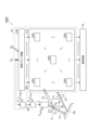
- FIG. 8 is a plan view showing the structure of each of the plurality of pixels 25A.
- a photoelectric conversion region 41 that converts pulsed light incident at the center into electric charges is provided, and the four corners of the pixel 25A around the photoelectric conversion region 41 are spaced apart from each other and close to the photoelectric conversion region 41.
- Four charge readout regions 43 1 to 43 4 are arranged.
- a charge discharge region for discharging the pixel from the photoelectric conversion region 41 is also arranged in the pixel 25A (not shown).
- control electrodes G1 to G4 are provided on both sides of the charge transfer path 45 between the photoelectric conversion region 41 and each of the charge readout regions 43 1 to 43 4 , and a charge discharge region is provided from the photoelectric conversion region 41 to the charge discharge region.
- a control electrode (not shown) is provided on the charge transfer path between the two.
- These four pairs of control electrodes G1 to G4 are connected to each other via the charge transfer path 45 from the photoelectric conversion region 41 when gate pulses D G1 , D G2 , D G3 , and D G4 are applied from the pixel driver circuit 13A. It functions as a potential forming means for forming a potential that transfers charges toward each of the charge readout regions 43 1 to 43 4 .
- the pixel 25A also includes a circuit (not shown) that reads out a charge signal (electrical signal) corresponding to the amount of accumulated charge from each of the charge readout regions 43 1 to 43 4 .
- the pixels 25A accumulate charge in the charge readout regions 43 1 to 43 4 at a predetermined timing such as the end of the frame period FR in accordance with a control signal given from a control circuit (not shown) in the image sensor 1A.
- a charge signal having a potential corresponding to the amount of charge thus obtained is outputted to the arithmetic circuit 7.
- the pixel 25A resets the charges accumulated in the charge readout regions 43 1 to 43 4 at the same time as outputting the charge signal.
- FIG. 9 shows the timing of the gate pulses D G1 , D G2 , D G3 , and D G4 generated by the pixel driver circuit 13A, and the arrival of the first light component L P1 and the second light component L P2 to the pixel 25. It is a timing chart explaining the relationship with timing.
- the pulsed light L P is irradiated from the light source 3 to the object Sa at a timing based on the clock pulse CL inputted from the outside, the first light component L P1 reflected by the object Sa, The directly incident second light component L P2 enters each pixel 25A of the image sensor 1A, and at the timing corresponding to the first light component L P1 and the second light component L P2 , the photoelectric current of each pixel 25A is generated.
- a photocurrent I PH is generated in the conversion region 41 .
- the pixel driver circuit 13A applies gate pulses D G1 and D G2 to each of the control electrodes G1 and G2 of each pixel 25A based on the irradiation timing of the pulsed light LP (timing of the trigger signal TR ) .
- the timings of the on-periods are set in advance so as to straddle the timing of generation of the photocurrent IPH by the second light component L P2 so as not to overlap with each other. Thereby, charges generated by the photocurrent I PH due to the second light component L P2 are distributed to the charge readout regions 43 1 and 43 2 of each pixel 25 .
- the pixel driver circuit 13A also controls the gate pulses D G3 and D G4 applied to the control electrodes G3 and G4 of each pixel 25A based on the irradiation timing of the pulsed light LP (timing of the trigger signal TR).
- the timing of the on-period is set in advance so as to span the generation timing of the photocurrent IPH by the first light component L P1 so as not to overlap with each other. Thereby, charges generated by the photocurrent I PH caused by the first light component L P1 are distributed to the charge readout regions 43 3 and 43 4 of each pixel 25 .
- the arithmetic circuit 7A selects the charge readout area 43 1 based on a set of charge signals corresponding to the amount of charge accumulated in the charge readout area 43 1 , 43 2 among the plurality of charge signals output from each pixel 25A . , 43 2 , the second time information TOF ref is calculated. Further, the arithmetic circuit 7A calculates the charge readout area based on a set of charge signals corresponding to the amount of charge accumulated in the charge readout areas 43 3 and 43 4 among the plurality of charge signals output from each pixel 25A.
- the first time information TOF sig is calculated by calculating the ratio of the amount of charge distributed to 43 3 and 43 4 .
- pulsed light is emitted at timings corresponding to the gate pulses D G1 , D G2 , D G3 , and D G4 under the control of the pixel driver circuit 13A.
- Charges converted from are accumulated in a plurality of charge readout regions 43 1 , 43 2 , 43 3 , 43 4 , and in the arithmetic circuit 7A, charges converted from the plurality of charge readout regions 43 1 , 43 2 , output from each pixel 25A are stored.
- First time information TOF sig and second time information TOF ref are calculated using a plurality of charge signals corresponding to the charges of 43 3 and 43 4 , and distance information is generated by taking the difference between them. . This makes it possible to generate highly accurate distance information with reduced effects of jitter.
- the arithmetic circuit 7A calculates first time information TOF sig based on a set of charge signals among the plurality of charge signals output from each pixel 25A, and The second time information TOF ref is calculated based on the set of .
- the time information TOF sig and TOF ref can be calculated based on the difference in the amount of charge accumulated at different timings in one set of charge readout regions in the pixel 25A, and the time information TOF sig and TOF ref can be calculated based on the time information. Highly accurate distance information can be generated.
- the detection operation of the plurality of pixels 25 may be continuously enabled without intermittently enabling the detection operation of the plurality of pixels 25 by the enable signal EN. good.
- the pixel 25 does not need to have an enabling function using the enable signal EN.
- the division ratio of the beam splitter 19 of the optical system 5 is set in advance so that two peak distributions appear in the histogram data created by the arithmetic circuit 7. According to such a modification, the configuration of the image sensor 1 can be simplified.
- each pixel 25A may have a configuration in which less than four sets of charge readout regions and control electrodes are provided.
- the pixel 25A may have two sets of charge readout regions and control electrodes.
- the pixel driver circuit 13A controls the phase of the gate pulse for each column of the pixels 25A in the sub-frame periods R1, S1, R2, S2, R3, S3,...Rn, Sn that temporally divide the frame period FR in order.
- the timing of the gate pulse is set to correspond to the arrival timing of the second light component L P2 in the subframe periods R1, R2, R3, ..., Rn
- the timing of the gate pulse is The timing of the gate pulse may be set to correspond to the arrival timing of the first optical component L P1 during the periods S1, S2, S3, . . . , Sn.
- the arithmetic circuit 7A calculates the second time information TOF ref based on a set of charge signals detected in the subframe periods R1, R2, R3, ..., Rn, and calculates the second time information TOF ref in the subframe periods S1, S2.
- S3, . . . , Sn can be used to calculate the first time information TOF sig , and highly accurate distance information can be generated based on the difference between the time information.
- the pixel driver circuit 13A sets the timing of the gate pulse for each row of the pixels 25A in addition to setting the timing of the gate pulse for each column of the pixels 25A.
- the acquisition of the first light component L P1 and the second light component L P2 may be switched over in time.
- the distance measuring device is not limited to one having a plurality of pixels, but can also be applied to a sensor having a single pixel.
- the configuration of an embodiment of a distance measuring device including a single pixel will be described below.
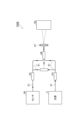
- FIG. 10 shows the configuration of a measurement system 100B according to the third embodiment.
- the measurement system 100B includes a sensor 1B composed of a single pixel, a light source 3, a waveguide 51 that optically connects the sensor 1B and the light source 3, optical elements A3, A4, A5, and A6, and a light projector. and a lens A7 with an integrated light receiving section.
- the pulsed light L P from the light source 3 is branched into a first light component L P1 and a second light component L P2 by an optical element A3 such as a coupler.
- the light emitting path to the object Sa and the light receiving path to the sensor 1B are combined by an optical element A6 such as a coupler, and the first light component L P1 is emitted to the object Sa using the lens A7.
- the reflected light of the first light component L P1 is received by using the light beam.
- the received first light component L P1 is combined with the second light component L P2 by an optical element A5 such as a coupler, and then input to the sensor 1B.
- the propagation direction of light may be limited by using a circulator or the like as the optical element A6.
- an isolator may be provided between the optical elements A3 to A6 to suppress return light.
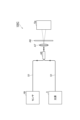
- FIG. 11 shows the configuration of a measurement system 100C according to the fourth embodiment
- FIG. 12 shows the configuration of a measurement system 100D according to the fifth embodiment
- the second light component L P2 is not formed by a waveguide but by an optical element A8 such as a cover glass disposed between the lens A7 and the object Sa. It may also be generated as return light by, for example.
- a histogram as shown in FIG. 6 is created based on the first light component L P1 reflected by the object Sa and the second light component L P2 generated as return light. is generated, and differential processing is performed based on the histogram.
- the measurement system 100D is configured to measure the distance of a transparent or translucent object, such as a liquid level, as the object Sa.
- an optical element A8 such as a cover glass is placed away from the object Sa on the opposite side of the lens A7 in order to generate return light based on the light that has passed through the object Sa.
- a histogram is generated based on the first light component L P1 reflected by the object Sa and the second light component L P2 generated as return light.
- the light source control circuit controls the generation timing to be a repeating timing, and the driver circuit controls a first period in which the first light component is detected with respect to the generation timing; It is preferable to apply the control signal so that the second period for detecting the second light component is set to be temporally separated from the generation timing. If such a configuration is adopted, the pixel is controlled to temporally separate the detection of the arrival timing of the first light component and the detection of the arrival timing of the second light component, and the difference between these detection results is calculated. This makes it possible to generate highly accurate distance information with reduced effects of jitter.
- the driver circuit apply a control signal so as to alternately and repeatedly set the first period and the second period.
- the pixel is controlled to alternately detect the arrival timing of the first light component and the arrival timing of the second light component, and by taking the difference between these detection results, the jitter is eliminated. It is possible to generate highly accurate distance information in which the influence of
- the arithmetic processing circuit calculates first time information based on the electrical signal detected in the first period, and calculates second time information based on the electrical signal detected in the second period. , is also preferable. According to such a configuration, by taking the difference between the first and second time information, it is possible to generate highly accurate distance information in which the influence of jitter is reduced.
- the pixel includes a photoelectric conversion element that photoelectrically converts pulsed light and a converter that converts the timing of the photoelectrically converted pulsed light into a digital signal, and outputs the digital signal as an electrical signal.
- a photoelectric conversion element that photoelectrically converts pulsed light
- a converter that converts the timing of the photoelectrically converted pulsed light into a digital signal
- the digital signal as an electrical signal.
- the light source control circuit controls the generation timing to be a repeating timing
- the driver circuit controls a first period in which the operation of the pixel is enabled at the arrival timing of the first light component with respect to the generation timing
- the control signal so that the second period for validating the pixel operation is set to be temporally separate from the arrival timing of the second light component relative to the generation timing.
- the pixel is controlled to temporally separate the detection of the arrival timing of the first light component and the detection of the arrival timing of the second light component, and the difference between the digital signals that are the results of these detections is controlled.
- the pixel corresponds to a photoelectric conversion region that converts pulsed light into charges, a plurality of charge readout regions provided close to the photoelectric conversion region and separated from each other, and a photoelectric conversion region and a plurality of charge readout regions. They each have a plurality of control electrodes for applying a plurality of control pulses for charge transfer between the photoelectric conversion region and the plurality of charge readout regions, and have a plurality of control electrodes for applying a plurality of control pulses for charge transfer between the photoelectric conversion region and the plurality of charge readout regions.
- the driver circuit applies a plurality of control pulses to the plurality of control electrodes, respectively, and the arithmetic processing circuit outputs the plurality of charge signals output from the pixels as electrical signals.
- the first time information based on the charge signals and calculate the second time information based on the plurality of charge signals.
- the charges converted from the pulsed light are accumulated in a plurality of charge readout areas at the timing corresponding to the control pulse, and the arithmetic processing circuit stores the charges output from the pixel.
- First and second time information are calculated using a plurality of charge signals corresponding to the charges in the readout region, and distance information is generated by taking the difference between them. This makes it possible to generate highly accurate distance information with reduced effects of jitter.
- the arithmetic processing circuit calculates first time information based on a set of charge signals among the plurality of charge signals, and calculates second time information based on a different set of charge signals among the plurality of charge signals. It is also preferable to calculate. According to this configuration, time information can be calculated based on the difference in the amount of charge accumulated at different timings in one set of charge readout areas, and highly accurate distance information can be generated based on the time information. .
- the light source control circuit controls the generation timing to be a repeating timing
- the driver circuit sets the timing of the plurality of control pulses to correspond to the arrival timing of the first light component with respect to the generation timing.
- the first period and the second period in which the timing of the plurality of control pulses is set to correspond to the arrival timing of the second light component with respect to the generation timing are set separately in time, and the arithmetic processing circuit
- the first time information may be calculated based on the plurality of charge signals detected in the first period
- the second time information may be calculated based on the plurality of charge signals detected in the second period. preferable.
- the pixel is controlled to temporally separate the detection of the arrival timing of the first light component and the detection of the arrival timing of the second light component, and the plurality of detection results are By taking the difference between the time information calculated based on the charge signal, it is possible to generate highly accurate distance information in which the influence of jitter is reduced.
- the distance measuring device of the present disclosure includes [1] a light source that generates pulsed light, a light source control circuit that controls the generation timing of the pulsed light, detects the arrival timing of the pulsed light, and generates an electrical signal corresponding to the arrival timing. Divide the output pixel and the pulsed light generated from the light source into a first light component that reflects off the object and enters the pixel, and a second light component that enters the pixel without passing through the object.
- An optical system, a driver circuit that applies a control signal to the pixel to control the detection operation of the pixel, and a calculation that generates distance information corresponding to the flight time of light to the target object based on the electrical signal output by the pixel.
- the arithmetic processing circuit is configured to generate first time information corresponding to the arrival timing of the first light component and arrival timing of the second light component based on the plurality of electrical signals output from the pixels. and second time information corresponding to the timing, and generates distance information by calculating the difference between the first time information and the second time information.
- the distance measuring device of the present disclosure has the following features: [2] “The light source control circuit controls the generation timing to be a repeating timing, and the driver circuit controls the first light component to detect the first light component with respect to the generation timing. and the second period for detecting the second light component with respect to the generation timing, which applies a control signal so as to set the period separately in time, and the distance measuring device according to [1] above. There may be.
- the distance measuring device of the present disclosure provides the distance measuring device according to [3] “The driver circuit applies the control signal so as to alternately and repeatedly set the first period and the second period. It may also be a “device”.
- the distance measuring device of the present disclosure includes [4] "The arithmetic processing circuit calculates first time information based on the electrical signal detected in the first period, and calculates the first time information based on the electrical signal detected in the second period.
- the distance measuring device according to [2] or [3] above, which calculates the second time information based on the distance measuring device.
- the distance measuring device of the present disclosure includes [5] "The pixel includes a photoelectric conversion element that photoelectrically converts pulsed light and a converter that converts the timing of the photoelectrically converted pulsed light into a digital signal, and the pixel converts the digital signal into an electrical signal.
- the distance measuring device according to any one of [1] to [4] above, which outputs a signal as a signal.
- the distance measuring device of the present disclosure has the following features: [6] "The light source control circuit controls the generation timing to be a repeating timing, and the driver circuit controls the operation of the pixel at the arrival timing of the first light component with respect to the generation timing. Applying a control signal so as to set a first period of activation and a second period of activation of the pixel at the arrival timing of the second light component with respect to the generation timing to be separated in time; The distance measuring device according to any one of [1] to [5] above may be used.
- the distance measuring device of the present disclosure includes [7] “The pixel includes a photoelectric conversion region that converts pulsed light into charges, a plurality of charge readout regions provided close to the photoelectric conversion region and spaced apart from each other, and a photoelectric conversion region.
- the driver circuit outputs a plurality of charge signals corresponding to the charges accumulated in the plurality of charge readout regions as electrical signals, the driver circuit applies a plurality of control pulses to the plurality of control electrodes, and the arithmetic processing circuit: Any of the above [1] to [4], wherein the first time information is calculated based on a plurality of charge signals output from a pixel, and the second time information is calculated based on the plurality of charge signals.
- the distance measuring device described in the above may be used.
- the distance measuring device of the present disclosure includes [8] "The arithmetic processing circuit calculates first time information based on a set of charge signals among the plurality of charge signals, and calculates first time information based on a set of charge signals among the plurality of charge signals, and The distance measuring device according to [7] above may calculate the second time information based on the set of .
- the distance measuring device of the present disclosure has the following features: [9] “The light source control circuit controls the generation timing to be a repeating timing, and the driver circuit controls the generation timing to correspond to the arrival timing of the first light component with respect to the generation timing. A first period in which the timing of the plurality of control pulses is set and a second period in which the timing of the plurality of control pulses is set so as to correspond to the arrival timing of the second light component with respect to the generation timing are temporally divided.
- the arithmetic processing circuit calculates first time information based on the plurality of charge signals detected in the first period, and calculates the second time information based on the plurality of charge signals detected in the second period.
- the distance measuring device described in [7] or [8] above may be used.
Abstract
A measuring system 100 comprises: a light source 3; a light source driver circuit 17; a plurality of pixels 25 that respectively output electrical signals corresponding to the arrival timing of pulsed light LP; an optical system 5 that splits the pulsed light LP into a first light component LP1 that reflects off of an object Sa and is incident on the pixels 25, and a second light component LP2 that is directly incident on the pixels 25; a pixel driver circuit 13 that applies a control signal for controlling a detection operation of the pixels 25; and a computation circuit 7 that generates distance information corresponding to the object Sa for each of the pixels 25. The computation circuit 7 calculates, on the basis of a plurality of electrical signals output from one pixel 25, time information TOFsig corresponding to the arrival timing of the first light component LP1, and time information TOFref corresponding to the arrival timing of the second light component LP2, and generates distance information by taking the difference between the two pieces of time information TOFsig and TOFref.
Description
本発明は、画素毎に距離情報を生成する距離計測装置及び距離計測方法に関する。
The present invention relates to a distance measuring device and a distance measuring method that generate distance information for each pixel.
従来から、光の飛行時間を用いて距離情報を含む画像信号を生成する装置が用いられている(例えば、下記特許文献1参照)。この下記特許文献1に記載の装置は、光源からパルス光を対象物に向けて照射させ、それに応じて発生した電荷を、制御パルスによって設定される異なる期間で画素内に蓄積し、蓄積されたそれぞれの電荷に対応した電気信号を読み出し、それらの電気信号を基に画素ごとの距離を計算することにより距離情報を取得する。なお、上記装置では、100μmを超える距離精度を実現しようとすると、制御パルスを画素に印加するためのドライバ回路におけるジッタが問題となる。そのため、上記装置は、画素が二次元的に配列された受光面が2つに分割され、一方の受光面に対象物で反射されたパルス光を入射させ、他方の受光面に基準面で反射されたパルス光を入射させ、それそれのパルス光を基に計算された距離演算値を差分することにより、距離演算値におけるジッタの影響を低減するように構成されている。
Conventionally, devices have been used that generate image signals including distance information using the flight time of light (for example, see Patent Document 1 below). The device described in Patent Document 1 below irradiates a target object with pulsed light from a light source, and accumulates the charges generated in response within pixels in different periods set by control pulses. Distance information is obtained by reading electrical signals corresponding to each charge and calculating the distance for each pixel based on these electrical signals. Note that in the above device, when attempting to achieve a distance accuracy of over 100 μm, jitter in the driver circuit for applying control pulses to pixels becomes a problem. Therefore, in the above device, the light-receiving surface on which pixels are arranged two-dimensionally is divided into two, and the pulsed light reflected by the object is incident on one light-receiving surface, and the pulsed light is reflected from the reference surface on the other light-receiving surface. It is configured to reduce the influence of jitter on the distance calculation value by inputting the pulsed light and calculating a difference between the distance calculation values calculated based on the respective pulsed lights.
上述した従来の装置においては、パルス光を空間的に分離して分離した成分を受光面上の別々の画素群に入射させる必要があり、複雑な光学系が必要になる傾向にあった。
In the conventional device described above, it is necessary to spatially separate the pulsed light and make the separated components enter separate pixel groups on the light receiving surface, which tends to require a complicated optical system.
本発明は、上記課題に鑑みて為されたものであり、光学系を複雑化させること無くジッタの影響が低減された高精度の距離情報を生成することが可能な距離計測装置及び距離計測方法を提供することを目的とする。
The present invention has been made in view of the above problems, and provides a distance measuring device and a distance measuring method that are capable of generating highly accurate distance information in which the influence of jitter is reduced without complicating the optical system. The purpose is to provide
上記課題を解決するため、本開示の一形態にかかる距離計測装置は、パルス光を発生させる光源と、パルス光の発生タイミングを制御する光源制御回路と、パルス光の到来タイミングを検出し、到来タイミングに対応した電気信号を出力する画素と、光源から発生したパルス光を、対象物を反射して画素に入射する第1の光成分と、画素に対象物を経由せずに入射する第2の光成分とに分割する光学系と、画素の検出動作を制御する制御信号を画素に印加するドライバ回路と、画素によって出力された電気信号を基に、対象物までの光の飛行時間に対応する距離情報を生成する演算処理回路と、を備え、演算処理回路は、画素から出力された複数の電気信号を基に、第1の光成分の到来タイミングに対応した第1の時間情報と、第2の光成分の到来タイミングに対応した第2の時間情報と、を計算し、第1の時間情報と第2の時間情報との差分を取ることにより距離情報を生成する。
In order to solve the above problems, a distance measuring device according to an embodiment of the present disclosure includes a light source that generates pulsed light, a light source control circuit that controls the generation timing of the pulsed light, and a light source that detects the arrival timing of the pulsed light and detects the arrival timing of the pulsed light. A pixel that outputs an electrical signal corresponding to the timing, a first light component that reflects pulsed light from a light source and enters the pixel, and a second light component that enters the pixel without passing through the object. An optical system that divides the light into two light components, a driver circuit that applies a control signal to the pixel that controls the detection operation of the pixel, and an electrical signal output by the pixel that corresponds to the flight time of the light to the target object. an arithmetic processing circuit that generates distance information based on the plurality of electrical signals output from the pixels, and the arithmetic processing circuit that generates first time information corresponding to the arrival timing of the first light component; second time information corresponding to the arrival timing of the second light component, and distance information is generated by calculating the difference between the first time information and the second time information.
あるいは、本開示の他の形態にかかる距離計測方法は、光源制御回路が、パルス光を発生させるように光源を制御する光源制御ステップと、光学系が、光源から発生したパルス光を、対象物を反射して画素に入射する第1の光成分と、画素に対象物を経由せずに入射する第2の光成分とに分割する光分割ステップと、パルス光の到来タイミングを検出し、到来タイミングに対応した電気信号を出力する画素を対象に、ドライバ回路が、画素の検出動作を制御する制御信号を画素に印加する信号印加ステップと、演算処理回路が、画素によって出力された電気信号を基に、対象物までの光の飛行時間に対応する距離情報を生成する演算処理ステップと、を備え、演算処理ステップでは、画素から出力された複数の電気信号を基に、第1の光成分の到来タイミングに対応した第1の時間情報と、第2の光成分の到来タイミングに対応した第2の時間情報と、を計算し、第1の時間情報と第2の時間情報との差分を取ることにより距離情報を生成する。
Alternatively, a distance measuring method according to another embodiment of the present disclosure includes a light source control step in which a light source control circuit controls the light source to generate pulsed light; and an optical system that directs the pulsed light generated from the light source toward the object. A light splitting step of dividing the light into a first light component that reflects and enters the pixel and a second light component that enters the pixel without passing through the object, and detecting the arrival timing of the pulsed light and detecting the arrival timing of the pulsed light. A signal application step in which the driver circuit applies a control signal to the pixel to control the detection operation of the pixel, and an arithmetic processing circuit applies the electric signal output by the pixel to the pixel that outputs the electric signal corresponding to the timing. and a calculation processing step for generating distance information corresponding to the flight time of light to the target object based on the plurality of electrical signals output from the pixels. The first time information corresponding to the arrival timing of the second light component and the second time information corresponding to the arrival timing of the second light component are calculated, and the difference between the first time information and the second time information is calculated. Generate distance information by taking
上記一形態の距離計測装置あるいは上記他の形態の距離計測方法によれば、光源からのパルス光に応じて対象物から生じた反射光である第1の光成分と、対象物を経由せずに直接入射する当該パルス光の第2の光成分とが画素に入射し、ドライバ回路から印加される制御信号によって動作する画素において、それに応じて、第1の光成分の到来タイミング及び第2の光成分の到来タイミングに対応した複数の電気信号が出力される。そして、演算処理回路において、画素から出力された複数の電気信号を用いて、第1及び第2の光成分のそれぞれの到来タイミングに対応した第1及び第2の時間情報が計算され、2つの時間情報の差分を取ることによって対象物までの光の飛行時間に対応する距離情報が生成される。このように、画素から出力された電気信号を対象とした電気的な処理により、パルス光を複数の画素上において空間的に分離すること無しに、距離情報におけるドライバ回路及び光源に起因するジッタ成分を削除することができる。その結果、光学系を複雑化させること無くジッタの影響が低減された高精度の距離情報を生成することができる。
According to the above-mentioned one form of distance measuring device or the above-mentioned other form of distance measuring method, the first light component, which is the reflected light generated from the object in response to the pulsed light from the light source, and the first light component that does not pass through the object. The second light component of the pulsed light that is directly incident on the pixel enters the pixel, and the pixel, which operates according to the control signal applied from the driver circuit, changes the arrival timing of the first light component and the second light component accordingly. A plurality of electrical signals corresponding to the arrival timing of the optical components are output. Then, in the arithmetic processing circuit, first and second time information corresponding to the respective arrival timings of the first and second light components are calculated using the plurality of electrical signals output from the pixels, and the two Distance information corresponding to the flight time of light to the target object is generated by taking the difference in time information. In this way, by electrical processing of electrical signals output from pixels, jitter components caused by driver circuits and light sources in distance information can be removed without spatially separating pulsed light on multiple pixels. can be deleted. As a result, highly accurate distance information with reduced jitter effects can be generated without complicating the optical system.
本発明によれば、光学系を複雑化させること無くジッタの影響が低減された高精度の距離情報を生成することができる。
According to the present invention, highly accurate distance information with reduced effects of jitter can be generated without complicating the optical system.
以下、図面を参照しつつ本発明に係る距離計測装置の好適な実施形態について詳細に説明する。なお、図面の説明においては、同一又は相当部分には同一符号を付し、重複する説明を省略する。
[第1実施形態] Hereinafter, preferred embodiments of a distance measuring device according to the present invention will be described in detail with reference to the drawings. In the description of the drawings, the same or corresponding parts are denoted by the same reference numerals, and redundant description will be omitted.
[First embodiment]
まず、図1を参照して、本開示の距離計測装置の第1実施形態に係る測定システム100の機能および構成の概要を説明する。図1に示す測定システム100は、対象物Saまでの距離をダイレクトTOF(Time Of Flight)法を用いて二次元的に検出するものであり、その検出結果を用いて二次元距離画像、あるいは三次元CADデータを生成するために用いられる。この測定システム100は、イメージセンサ(撮像素子)1と、パルス光を照射する光源3と、パルス光を対象物Sa及びイメージセンサ1に導くための光学システム(光学系)5と、距離情報を演算する演算回路(演算処理回路)7と、遅延調整回路9と、を含んで構成されている。
First, with reference to FIG. 1, an overview of the functions and configuration of a measurement system 100 according to a first embodiment of a distance measurement device of the present disclosure will be described. The measurement system 100 shown in FIG. 1 detects the distance to the target object Sa two-dimensionally using the direct TOF (Time Of Flight) method, and uses the detection results to create a two-dimensional distance image or a three-dimensional Used to generate original CAD data. This measurement system 100 includes an image sensor (imaging device) 1, a light source 3 that emits pulsed light, an optical system (optical system) 5 that guides the pulsed light to the object Sa and the image sensor 1, and a distance information It is configured to include an arithmetic circuit (arithmetic processing circuit) 7 that performs calculations and a delay adjustment circuit 9.
光源3は、TOF法による距離計測を行うために、対象物Saに照射するパルス光LPを発生させる装置である。光源3は、例えば、発光ダイオードあるいはレーザダイオード等の半導体発光素子とその半導体発光素子を駆動する駆動回路とによって構成される。光源3としては、近赤外領域、可視光領域等の波長領域の光を発生させる素子を用いることができる。この光源3は、例えば、パルス幅100psecのパルス光を照射可能に構成されている。なお、光源3の照射する光のパルス幅は上記値には限定されず、様々な値に設定され得る。
The light source 3 is a device that generates pulsed light LP that is irradiated onto the object Sa in order to perform distance measurement using the TOF method. The light source 3 is constituted by, for example, a semiconductor light emitting element such as a light emitting diode or a laser diode, and a drive circuit that drives the semiconductor light emitting element. As the light source 3, an element that generates light in a wavelength region such as a near-infrared region or a visible light region can be used. This light source 3 is configured to be able to emit pulsed light with a pulse width of 100 psec, for example. Note that the pulse width of the light emitted by the light source 3 is not limited to the above value, and can be set to various values.
イメージセンサ1は、受光面11と、画素ドライバ回路13と、光源ドライバ回路(光源制御回路)17とを含んで構成され、これらの回路は同一の半導体チップ上、もしくは3次元的に積層されたチップ上に集積化されて構成される。なお、演算回路7は、イメージセンサ1の外部の回路上に構成されているが、イメージセンサ1とともに同一の半導体チップ上に集積化されていてもよい。
The image sensor 1 includes a light receiving surface 11, a pixel driver circuit 13, and a light source driver circuit (light source control circuit) 17, and these circuits are arranged on the same semiconductor chip or three-dimensionally stacked. It is integrated and configured on a chip. Note that although the arithmetic circuit 7 is configured on a circuit outside the image sensor 1, it may be integrated on the same semiconductor chip together with the image sensor 1.
受光面11は、二次元的に配置された複数の画素25を有する。詳細には、受光面11は、NV行NH列(NV,NHは2以上の整数)で2次元マトリクス状に配列された複数の画素25によって構成され、方形状の撮像領域を構成する。これらの画素25には、それぞれ、画素ドライバ回路13から画素25の検出動作を制御する制御信号が印加される。
The light receiving surface 11 has a plurality of pixels 25 arranged two-dimensionally. Specifically, the light-receiving surface 11 is composed of a plurality of pixels 25 arranged in a two-dimensional matrix in N V rows and N H columns (N V and N H are integers of 2 or more), and forms a rectangular imaging area. Configure. A control signal for controlling the detection operation of the pixels 25 is applied from the pixel driver circuit 13 to each of these pixels 25 .
画素ドライバ回路13は、イメージセンサ1の外部から入力されたクロックパルスCLを基に受光面11の各画素25におけるパルス光の検出動作を有効化(制御)するための複数のイネーブル信号(制御信号)ENを生成および出力する。本実施形態では、画素ドライバ回路13は、全画素25に共通な複数のイネーブル信号ENを、周期的なフレーム期間内でパルス状の電圧信号として繰り返し生成する。このイネーブル信号ENのパルス幅は、画素25に対してフォトンを検出可能に制御できる程度の時間幅に設定される。例えば、画素ドライバ回路13は、受光面11上の画素25の列毎に共通のイネーブル信号ENを生成し、画素25の列毎にイネーブル信号ENを印加する。
The pixel driver circuit 13 generates a plurality of enable signals (control signals) for enabling (controlling) the pulsed light detection operation in each pixel 25 of the light receiving surface 11 based on the clock pulse CL input from the outside of the image sensor 1. ) generate and output EN. In this embodiment, the pixel driver circuit 13 repeatedly generates a plurality of enable signals EN common to all pixels 25 as pulse-like voltage signals within a periodic frame period. The pulse width of the enable signal EN is set to such a time width that the pixel 25 can be controlled to detect photons. For example, the pixel driver circuit 13 generates a common enable signal EN for each column of pixels 25 on the light-receiving surface 11, and applies the enable signal EN to each column of pixels 25.
光源ドライバ回路17は、外部から入力されたクロックパルスCLを基に、光源3によるパルス光LPの照射(発生)タイミングを制御するトリガー信号TRを生成し、そのトリガー信号TRを光源3に供給する。ここで、光源ドライバ回路17は、上述した周期的なフレーム期間内で複数のイネーブル信号ENに同期したパルス状の電圧信号であるトリガー信号TRを繰り返し生成する。また、光源ドライバ回路17は、トリガー信号TRを、光源3に供給すると同時に、画素25の検出動作の制御のために、受光面11上の画素25に対しても供給する。
The light source driver circuit 17 generates a trigger signal TR that controls the irradiation (generation) timing of the pulsed light LP by the light source 3 based on the clock pulse CL input from the outside, and supplies the trigger signal TR to the light source 3. do. Here, the light source driver circuit 17 repeatedly generates the trigger signal TR, which is a pulsed voltage signal synchronized with the plurality of enable signals EN, within the periodic frame period described above. Further, the light source driver circuit 17 supplies the trigger signal TR to the light source 3 and also to the pixels 25 on the light receiving surface 11 in order to control the detection operation of the pixels 25.
遅延調整回路9は、イメージセンサ1の光源ドライバ回路17と光源3との間に電気的に接続されている。この遅延調整回路9は、イメージセンサ1から出力されるトリガー信号TRに遅延を生じさせ、この遅延の時間幅を可変に調整する。遅延調整回路9は、イメージセンサ1内で生じるイネーブル信号EN及びトリガー信号TRの信号遅延に対応してパルス光LPの発光タイミングを調整するために設けられる。この遅延調整回路9は、イメージセンサ1を構成する半導体チップ内に集積化されていてもよいし、その半導体チップ外の回路に集積化されていてもよい。
The delay adjustment circuit 9 is electrically connected between the light source driver circuit 17 of the image sensor 1 and the light source 3. This delay adjustment circuit 9 causes a delay in the trigger signal TR output from the image sensor 1, and variably adjusts the time width of this delay. The delay adjustment circuit 9 is provided to adjust the emission timing of the pulsed light LP in response to signal delays of the enable signal EN and the trigger signal TR occurring within the image sensor 1. This delay adjustment circuit 9 may be integrated within the semiconductor chip constituting the image sensor 1, or may be integrated into a circuit outside the semiconductor chip.
光学システム5は、ビームスプリッタ19、光導波路21、及びレンズ23,27を含んでいる。ビームスプリッタ19は、光源3から照射されたパルス光LPを、対象物Saに入射する第1の光成分LP1と、対象物Saを経由せずに直接受光面11に入射する第2の光成分LP2とに分割する光分割素子である。ビームスプリッタ19としては、例えば、所定の分割割合(反射率、透過率)を有するハーフミラーである。レンズ23は、ビームスプリッタ19によって分割された第1の光成分LP1の照射範囲を、対象物Saの存在する範囲に設定するレンズである。レンズ27は、対象物Saによって反射されて戻ってきた第1の光成分LP1を、受光面11上の少なくとも一部の複数の画素25に入射するように集光するレンズである。光導波路21は、ビームスプリッタ19によって分割された第2の光成分LP2を、受光面11上の少なくとも一部の複数の画素25であって、第1の光成分LP1が入射する複数の画素25と同一の複数の画素25に導光する光学素子である。光導波路21としては、例えば、光ファイバが用いられる。光ファイバで光導波路21を構築する際には,光アイソレータなどを用いて光を一方向に伝播するように構成されてもよい。
Optical system 5 includes a beam splitter 19, an optical waveguide 21, and lenses 23 and 27. The beam splitter 19 splits the pulsed light L P emitted from the light source 3 into a first light component L P1 that is incident on the object Sa and a second light component L P1 that is directly incident on the light receiving surface 11 without passing through the object Sa. This is a light splitting element that splits the light into light components L and P2 . The beam splitter 19 is, for example, a half mirror having a predetermined splitting ratio (reflectance, transmittance). The lens 23 is a lens that sets the irradiation range of the first light component L P1 divided by the beam splitter 19 to the range where the object Sa exists. The lens 27 is a lens that condenses the first light component L P1 reflected and returned by the object Sa so that it enters at least some of the pixels 25 on the light receiving surface 11 . The optical waveguide 21 directs the second light component L P2 split by the beam splitter 19 to at least some of the pixels 25 on the light receiving surface 11, into which the first light component L P1 is incident. This is an optical element that guides light to the same plurality of pixels 25 as the pixel 25. As the optical waveguide 21, for example, an optical fiber is used. When constructing the optical waveguide 21 using an optical fiber, an optical isolator or the like may be used to propagate light in one direction.
ここで、イメージセンサ1のそれぞれの画素25の構成について詳細に説明する。図2は、画素25の機能構成を示すブロック図であり、図3は、画素25の回路構成を示す回路図である。
Here, the configuration of each pixel 25 of the image sensor 1 will be described in detail. FIG. 2 is a block diagram showing the functional configuration of the pixel 25, and FIG. 3 is a circuit diagram showing the circuit configuration of the pixel 25.
図2に示すように、画素25は、光電変換素子であるSPAD(Single Photon Avalanche Diode)29と波形整形器31とTDC(Time to Digital Converter、変換器)33とを含んで構成される。SPAD29は、入射するフォトンに応じて光電変換してパルス電圧(電気信号)を生成する受光素子である。波形整形器31は、SPAD29の後段に電気的に接続され、SPAD29によって生成されたパルス電圧を増幅および整形して増幅パルス電圧(電気信号)を生成する。TDC33は、光源ドライバ回路17から入力されたトリガー信号TRのタイミングから、波形整形器31によって生成された増幅パルス電圧のタイミングまでの時間をカウントし、そのカウント値をデジタル信号(電気信号)DCに変換して出力する。このような構成の画素25は、光源3の照射タイミングを基準とした、画素25に入射する第1の光成分LP1及び第2の光成分LP2の到来タイミングを検出することができ、検出結果をデジタル信号(電気信号)DCとして出力することができる。
As shown in FIG. 2, the pixel 25 includes a SPAD (Single Photon Avalanche Diode) 29, which is a photoelectric conversion element, a waveform shaper 31, and a TDC (Time to Digital Converter) 33. The SPAD 29 is a light receiving element that photoelectrically converts incident photons to generate a pulse voltage (electrical signal). The waveform shaper 31 is electrically connected after the SPAD 29 and amplifies and shapes the pulse voltage generated by the SPAD 29 to generate an amplified pulse voltage (electrical signal). The TDC 33 counts the time from the timing of the trigger signal TR input from the light source driver circuit 17 to the timing of the amplified pulse voltage generated by the waveform shaper 31, and converts the count value into a digital signal (electrical signal) DC. Convert and output. The pixel 25 having such a configuration can detect the arrival timing of the first light component L P1 and the second light component L P2 that are incident on the pixel 25 based on the irradiation timing of the light source 3. The result can be output as a digital signal (electrical signal) DC .
また、画素25は、画素ドライバ回路13からSPAD29に対して複数のイネーブル信号ENが入力されるように構成されている。SPAD29は、入力されたイネーブル信号ENがオンの期間において、入射するフォトンを検出してパルス電圧を生成し、入力されたイネーブル信号ENがオフの期間においては、パルス電圧を生成しないように(フォトンを検出しないように)構成される。ただし、画素25は、イネーブル信号ENによって、第1の光成分LP1及び第2の光成分LP2の検出動作が有効化されるように構成されていればよく、TDC33あるいは波形整形器31の動作がイネーブル信号ENによって有効化されるように構成されていてもよい。
Furthermore, the pixel 25 is configured such that a plurality of enable signals EN are input from the pixel driver circuit 13 to the SPAD 29. The SPAD 29 detects incident photons and generates a pulse voltage during a period when the input enable signal EN is on, and does not generate a pulse voltage (photons) during a period when the input enable signal EN is off. configured so as not to detect However, the pixel 25 only needs to be configured so that the detection operation of the first light component L P1 and the second light component L P2 is enabled by the enable signal EN, and the pixel 25 is configured so that the detection operation of the first light component L P1 and the second light component L P2 is enabled by the enable signal EN. The operation may be configured to be enabled by an enable signal EN.
画素25の具体的回路構成としては、図3に示す構成を採用することができる。詳細には、SPAD29は、アバランシェダイオードによって構成される。SPAD29のカソードには、NチャネルMOSトランジスタであるスイッチング素子35を介してアノード電位よりも高く設定されたカソード電位VDD_SPADが印加される。さらに、SPAD29のカソードは、NチャネルMOSトランジスタであるスイッチング素子37を介して波形整形器31の入力に接続される。スイッチング素子35は、イネーブル信号ENに応じてスイッチングするように構成され、スイッチング素子37は、イネーブル信号に同期するように生成されたイネーブル信号ENdに応じてスイッチングするように構成される。波形整形器31は、SPAD29のカソード電圧を反転して増幅する反転増幅器として構成される。
As a specific circuit configuration of the pixel 25, the configuration shown in FIG. 3 can be adopted. Specifically, the SPAD 29 is constituted by an avalanche diode. A cathode potential V DD_SPAD set higher than the anode potential is applied to the cathode of the SPAD 29 via a switching element 35 which is an N-channel MOS transistor. Further, the cathode of the SPAD 29 is connected to the input of the waveform shaper 31 via a switching element 37 that is an N-channel MOS transistor. The switching element 35 is configured to switch in response to an enable signal EN, and the switching element 37 is configured to switch in response to an enable signal ENd generated in synchronization with the enable signal. The waveform shaper 31 is configured as an inverting amplifier that inverts and amplifies the cathode voltage of the SPAD 29.
図3に示す構成の画素25の動作を、波形図を参照して説明する。図4は、画素25の動作を説明するための各種信号の時間変化を示すタイミングチャートである。TDC33は、トリガー信号TRがオンされたタイミングで時間のカウントを開始する。イネーブル信号ENがハイ状態になると、それに同期してイネーブル信号ENdが遅延してハイ状態となり、スイッチング素子35,37が導通状態とされ、SPAD29のカソード電位VKが電位VDD_SPADに高く設定される。この状態でSPAD29にフォトンが入射すると、アバランシェ増倍した光電流によってカソード電位VKが低下し、スイッチング素子37を介してカソード電位VKが波形整形器31に入力されることにより、波形整形器31からパルス状に電位が上昇する増幅パルス電圧VPが出力される。TDC33は、この増幅パルス電圧VPの電圧上昇タイミングでカウントを停止し、トリガー信号TRのタイミングからフォトンの入射タイミングの間の時間差Ttotを計測し、デジタル信号DCとして出力する。一方で、イネーブル信号ENがロー状態の場合には、SPAD29にフォトンが入射しても、カソード電位VKがスイッチング素子37によって遮断される結果、TDC33に入力される増幅パルス電圧VPには反映されないため、その際のフォトンの入射に応じたカウント値は出力されない。
The operation of the pixel 25 having the configuration shown in FIG. 3 will be explained with reference to waveform diagrams. FIG. 4 is a timing chart showing temporal changes in various signals for explaining the operation of the pixel 25. As shown in FIG. The TDC 33 starts counting time at the timing when the trigger signal TR is turned on. When the enable signal EN becomes a high state, the enable signal ENd is delayed and becomes a high state in synchronization with it, the switching elements 35 and 37 are made conductive, and the cathode potential VK of the SPAD 29 is set high to the potential VDD_SPAD . . When a photon enters the SPAD 29 in this state, the cathode potential VK decreases due to the avalanche-multiplied photocurrent, and the cathode potential VK is input to the waveform shaper 31 via the switching element 37, causing the waveform shaper to 31 outputs an amplified pulse voltage VP whose potential increases in a pulsed manner. The TDC 33 stops counting at the voltage rise timing of this amplified pulse voltage VP , measures the time difference T tot between the timing of the trigger signal TR and the timing of incidence of the photon, and outputs it as a digital signal DC . On the other hand, when the enable signal EN is in a low state, even if a photon is incident on the SPAD 29, the cathode potential VK is blocked by the switching element 37, so that it is not reflected in the amplified pulse voltage VP input to the TDC 33. Therefore, the count value corresponding to the incident photon at that time is not output.
次に、画素ドライバ回路13及び光源ドライバ回路17による制御信号の生成機能について説明する。図5は、画素ドライバ回路13及び光源ドライバ回路17によって生成されるイネーブル信号EN及びトリガー信号TRの時間波形を示すタイミングチャートである。
Next, the control signal generation function by the pixel driver circuit 13 and the light source driver circuit 17 will be explained. FIG. 5 is a timing chart showing the time waveforms of the enable signal EN and trigger signal TR generated by the pixel driver circuit 13 and the light source driver circuit 17.
図5に示されるように、画素ドライバ回路13及び光源ドライバ回路17は、所定周期で繰り返されるフレーム期間FRごとに所定のタイミングでイネーブル信号EN及びトリガー信号TRを生成する機能を有する。すなわち、光源ドライバ回路17は、光源3でのパルス光LPの発生タイミングが、フレーム期間FRを時間的に順番に区切ったサブフレーム期間R1,S1,R2,S2,R3,S3,…Rn,Sn(nは、2以上の整数)において、所定周期の繰り返しのタイミングになるように、トリガー信号TRを生成する。また、画素ドライバ回路13は、パルス光LPの発生タイミングに対して第2の光成分LP2の到来タイミングを含む期間Trefに重なるようにイネーブル信号ENのオン期間を設定するサブフレーム期間(第2の期間)R1,R2,R3,…Rnと、パルス光LPの発生タイミングに対して第1の光成分LP1の到来タイミングを含む期間Tsigに重なるようにイネーブル信号ENのオン期間を設定するサブフレーム期間(第1の期間)S1,S2,S3,…Snとが時間的に分けて設定されるように、イネーブル信号ENを生成する。このような機能により、サブフレーム期間(第2の期間)R1,R2,R3,…Rnにおいては、第2の光成分LP2の到来タイミングにおいて画素25の検出動作が有効化されて第2の光成分LP2の到来タイミングが検出され、サブフレーム期間(第1の期間)S1,S2,S3,…Snにおいては、第1の光成分LP1の到来タイミングにおいて画素25の検出動作が有効化されて第1の光成分LP1の到来タイミングが検出される。より詳細には、画素ドライバ回路13は、サブフレーム期間R1,R2,R3,…Rnとサブフレーム期間S1,S2,S3,…Snとが、交互に繰り返し設定されるように、イネーブル信号ENを生成する。
As shown in FIG. 5, the pixel driver circuit 13 and the light source driver circuit 17 have a function of generating an enable signal EN and a trigger signal TR at a predetermined timing for each frame period FR that is repeated at a predetermined cycle. That is, the light source driver circuit 17 determines that the timing of generation of the pulsed light LP in the light source 3 is determined by sub-frame periods R1, S1, R2, S2, R3, S3,...Rn, which are temporally sequentially divided frame periods FR. At Sn (n is an integer of 2 or more), the trigger signal TR is generated at a repeating timing of a predetermined period. Further, the pixel driver circuit 13 sets the on-period of the enable signal EN so as to overlap the period Tref including the arrival timing of the second light component LP2 with respect to the generation timing of the pulsed light LP . (period 2) R1, R2, R3,...Rn, and the on-period of the enable signal EN is set so as to overlap with the period Tsig that includes the arrival timing of the first optical component L P1 with respect to the generation timing of the pulsed light L P The enable signal EN is generated so that the subframe periods (first periods) S1, S2, S3, . . . Sn are set separately in time. With such a function, in the subframe periods (second periods) R1, R2, R3,...Rn, the detection operation of the pixel 25 is enabled at the arrival timing of the second light component L P2 , and the second light component L P2 is activated. The arrival timing of the light component L P2 is detected, and in subframe periods (first periods) S1, S2, S3, ... Sn, the detection operation of the pixel 25 is enabled at the arrival timing of the first light component L P1 . Then, the arrival timing of the first light component L P1 is detected. More specifically, the pixel driver circuit 13 sets the enable signal EN so that the subframe periods R1, R2, R3, ...Rn and the subframe periods S1, S2, S3, ...Sn are alternately and repeatedly set. generate.
図1に戻って、演算回路7は、複数の画素25のそれぞれからフレーム期間FRの間に出力されたデジタル信号DCを基に対象物Saまでのパルス光LPの飛行時間に対応する距離情報を、複数の画素毎に生成する。すなわち、演算回路7は、複数の画素25のそれぞれからフレーム期間FRの間に繰り返し出力された複数のデジタル信号DCを対象に、デジタル信号DCの示すカウント値の度数を集計したヒストグラムデータを作成する。図6は、演算回路7によって画素25毎にフレーム期間FRを対象に作成されたヒストグラムデータを示すグラフである。このように、ヒストグラムデータにおいては、第1の光成分LP1の到来タイミングに対応する分布DT1と、第2の光成分LP2の到来タイミングに対応する分布DT2とが現れる。このような性質を利用し、演算回路7は、カウント値が小さい方の分布DT2を対象に代表値を計算し、その代表値を基に第2の光成分LP2の飛行時間に対応する時間情報TOFrefを取得する。加えて、演算回路7は、カウント値が大きい方の分布DT1を対象に代表値を計算し、その代表値を基に第1の光成分LP1の飛行時間に対応する時間情報TOFsigを取得する。ここで、演算回路7は、分布DT1,DT2における代表値として平均値を計算してもよいし、中央値のような他の代表値を計算してもよい。さらに、演算回路7は、画素25毎に取得した時間情報TOFsigと時間情報TOFrefとの差分を取ることにより、距離情報を生成する。演算回路7は、フレーム期間FRを対象に計算した全画素25の距離情報を基に、最終的に二次元距離画像あるいは三次元CADデータを生成および出力する。
Returning to FIG. 1, the arithmetic circuit 7 determines the distance corresponding to the flight time of the pulsed light LP to the object Sa based on the digital signal DC output from each of the plurality of pixels 25 during the frame period FR. Information is generated for each plurality of pixels. That is, the arithmetic circuit 7 calculates histogram data obtained by summing up the frequencies of count values indicated by the digital signals DC for the plurality of digital signals DC repeatedly output from each of the plurality of pixels 25 during the frame period FR. create. FIG. 6 is a graph showing histogram data created by the arithmetic circuit 7 for each pixel 25 over the frame period FR. In this way, in the histogram data, a distribution DT 1 corresponding to the arrival timing of the first light component L P1 and a distribution DT 2 corresponding to the arrival timing of the second light component L P2 appear. Utilizing such properties, the arithmetic circuit 7 calculates a representative value for the distribution DT2 with the smaller count value, and based on the representative value, corresponds to the flight time of the second light component L P2 . Obtain time information TOF ref . In addition, the arithmetic circuit 7 calculates a representative value for the distribution DT1 with the larger count value, and based on the representative value, calculates time information TOF sig corresponding to the flight time of the first light component L P1 . get. Here, the arithmetic circuit 7 may calculate an average value as a representative value in the distributions DT 1 and DT 2 , or may calculate another representative value such as a median value. Furthermore, the arithmetic circuit 7 generates distance information by taking the difference between the time information TOF sig and the time information TOF ref acquired for each pixel 25. The arithmetic circuit 7 finally generates and outputs a two-dimensional distance image or three-dimensional CAD data based on the distance information of all pixels 25 calculated for the frame period FR.
なお、演算回路7は、1つのフレーム期間FR内のサブフレーム期間R1,R2,R3,…Rnの間に検出されたデジタル信号DCを基に1つのヒストグラムデータを作成し、そのヒストグラムデータに現れる第2の光成分LP2の到来タイミングに対応する分布DT2を対象に時間情報TOFrefを取得することもできる。また、演算回路7は、1つのフレーム期間FR内のサブフレーム期間S1,S2,S3,…Snの間に検出されたデジタル信号DCを基に別のヒストグラムデータを作成し、そのヒストグラムデータに現れる第1の光成分LP1の到来タイミングに対応する分布DT1を対象に時間情報TOFsigを取得することもできる。
Note that the arithmetic circuit 7 creates one histogram data based on the digital signal DC detected during the sub-frame periods R1, R2, R3,...Rn within one frame period FR, and applies the histogram data to the histogram data. It is also possible to acquire the time information TOF ref for the distribution DT 2 corresponding to the arrival timing of the appearing second light component L P2 . Further, the arithmetic circuit 7 creates another histogram data based on the digital signal DC detected during the sub-frame periods S1, S2, S3,...Sn within one frame period FR, and uses the histogram data as It is also possible to obtain the time information TOF sig for the distribution DT 1 corresponding to the arrival timing of the first light component L P1 that appears.
次に、本実施形態に係る距離計測方法の手順を説明する。本実施形態の距離計測方法は、次のステップを含む。まず、光源ドライバ回路17が、フレーム期間FR内で繰り返しパルス光LPを発生させるように光源3を制御する(光源制御ステップ)。光源3から発生したパルス光LPは、光学システム5によって、第1の光成分LP1及び第2の光成分LP2に分割された後に、第1の光成分LP1は対象物Saの存在する範囲に向けて照射され、第2の光成分LP2は対象物Saを経由せずに画素25に向けて直接導光される(光分割ステップ)。また、画素ドライバ回路13によって、フレーム期間FRを時間的に区切ったサブフレーム期間R1,S1,R2,S2,R3,S3,…Rn,Snにおいて、所定周期の繰り返しのタイミングになるように、イネーブル信号ENが生成され、イネーブル信号ENが複数の画素25に印加される(信号印加ステップ)。さらに、演算回路7により、複数の画素25毎にフレーム期間FRに対応して出力されたデジタル信号DCを基に、ヒストグラムデータが生成され、ヒストグラムデータを用いて2つの時間情報TOFsig,TOFrefが取得される。そして、演算回路7により、画素毎の2つの時間情報TOFsig,TOFrefの差分を取ることにより距離情報が生成され、フレーム期間FRを対象に計算した全画素25の距離情報を基に二次元距離画像あるいは三次元CADデータが生成および出力される(演算処理ステップ)。
Next, the procedure of the distance measuring method according to this embodiment will be explained. The distance measuring method of this embodiment includes the following steps. First, the light source driver circuit 17 controls the light source 3 to repeatedly generate pulsed light LP within the frame period FR (light source control step). After the pulsed light L P generated from the light source 3 is divided into a first light component L P1 and a second light component L P2 by an optical system 5, the first light component L P1 is divided into a first light component L P1 and a second light component L P2 . The second light component L P2 is directly guided toward the pixel 25 without passing through the object Sa (light splitting step). In addition, the pixel driver circuit 13 controls the enable timing so that the repetition timing of a predetermined period is reached in the sub-frame periods R1, S1, R2, S2, R3, S3, ... Rn, Sn that temporally divide the frame period FR. A signal EN is generated and the enable signal EN is applied to the plurality of pixels 25 (signal application step). Further, the arithmetic circuit 7 generates histogram data based on the digital signal DC output for each of the plurality of pixels 25 corresponding to the frame period FR, and uses the histogram data to generate two time information TOF sig and TOF. A ref is obtained. Distance information is then generated by the arithmetic circuit 7 by taking the difference between the two time information TOF sig and TOF ref for each pixel, and two-dimensional information is generated based on the distance information of all pixels 25 calculated for the frame period FR. A distance image or three-dimensional CAD data is generated and output (computation processing step).
ここで、本実施形態の測定システム100及びそれを用いた距離計測方法の作用効果について説明する。
Here, the effects of the measurement system 100 of this embodiment and the distance measurement method using the same will be explained.
測定システム100及びそれを用いた距離計測方法によれば、光源3からのパルス光LPに応じて対象物Saから生じた反射光である第1の光成分LP1と、対象物Saを経由せずに直接入射する当該パルス光LPの第2の光成分LP2とが複数の画素25に入射し、画素ドライバ回路13から印加されるイネーブル信号ENによって動作する複数の画素25のそれぞれにおいて、それに応じて、第1の光成分LP1の到来タイミング及び第2の光成分LP2の到来タイミングに対応した複数のデジタル信号DCが出力される。そして、演算回路7において、複数の画素25のそれぞれから出力された複数のデジタル信号DCを用いて、第1の光成分LP1及び第2の光成分LP2のそれぞれの到来タイミングに対応した第1の時間情報TOFsig及び第2の時間情報TOFrefが計算され、2つの時間情報TOFsig,TOFrefの差分を取ることによって対象物Saまでの光の飛行時間に対応する距離情報が生成される。このように、画素25のそれぞれから出力された複数のデジタル信号DCを対象とした電気的な処理により、パルス光LPを複数の画素25上において空間的に分離すること無しに、距離情報における光源ドライバ回路17、遅延調整回路9、光源3、及びイメージセンサ1内の制御信号分配回路に起因するジッタ成分あるいは温度ドリフト成分を削除することができる。その結果、光学系を複雑化させること無くジッタの影響が低減された高精度の距離情報を生成することができる。特に、パルス光を空間的に分離する複雑な光学系、あるいは、分離したパルス光の受光面11への入射範囲を互いに制限するマスク等の光学部材が不要とされる。
According to the measurement system 100 and the distance measurement method using the same, the first light component L P1 , which is the reflected light generated from the object Sa in response to the pulsed light L P from the light source 3, The second light component L P2 of the pulsed light L P directly enters the plurality of pixels 25 , and in each of the plurality of pixels 25 operated by the enable signal EN applied from the pixel driver circuit 13 . Accordingly, a plurality of digital signals DC corresponding to the arrival timing of the first optical component L P1 and the arrival timing of the second optical component L P2 are output. Then, in the arithmetic circuit 7, using the plurality of digital signals DC output from each of the plurality of pixels 25, a signal is generated corresponding to the arrival timing of each of the first light component L P1 and the second light component L P2 . The first time information TOF sig and the second time information TOF ref are calculated, and distance information corresponding to the flight time of the light to the object Sa is generated by taking the difference between the two time information TOF sig and TOF ref . be done. In this way, by electrically processing the plurality of digital signals DC output from each of the pixels 25, distance information can be obtained without spatially separating the pulsed light LP on the plurality of pixels 25. It is possible to eliminate jitter components or temperature drift components caused by the light source driver circuit 17, the delay adjustment circuit 9, the light source 3, and the control signal distribution circuit in the image sensor 1. As a result, highly accurate distance information with reduced jitter effects can be generated without complicating the optical system. In particular, a complicated optical system that spatially separates the pulsed lights or an optical member such as a mask that limits the range of incidence of the separated pulsed lights on the light-receiving surface 11 is not required.
具体的には、本実施形態によれば、光源ドライバ回路17及び遅延調整回路9から光源3に与えるトリガー信号TR、及び、光源ドライバ回路17から受光面11に与えるトリガー信号TRにおいて生じるクロックジッタによる距離演算値の揺らぎを除去することができる。すなわち、クロックジッタは、光源3内のトリガー受信回路及びレーザダイオード等の発光素子の駆動回路において生じるゆらぎδLMと、遅延調整回路9におけるゆらぎδDLCと、イメージセンサ1内の光源ドライバ回路17におけるゆらぎδTRIGとが主な原因となる。特に、1/fゆらぎをもつクロックジッタは複数のフレーム期間FRの間で距離情報を平均して最終的な距離を求めるフレーム平均を用いても低減ができないため、従来の距離計測装置における計測精度はクロックジッタで律速されてしまう傾向にあった。本実施形態においては、第2の光成分LP2を検出して計算される時間情報TOFrefにおける変化は、第2の光成分LP2の光路長が固定されているために、クロックジッタを要因とするゆらぎの成分と一致する。そのため、2つの時間情報TOFsig,TOFrefの差分をとれば、共通部分のクロックジッタの成分を除去することができ、距離分解能を画素におけるショットノイズのみで決まる理論限界までに向上できる。
Specifically, according to the present embodiment, clock jitter occurs in the trigger signal TR given to the light source 3 from the light source driver circuit 17 and the delay adjustment circuit 9, and in the trigger signal TR given from the light source driver circuit 17 to the light receiving surface 11. Fluctuations in distance calculation values can be removed. That is, the clock jitter is caused by fluctuations δ LM occurring in the trigger receiving circuit in the light source 3 and the driving circuit of the light emitting element such as a laser diode, fluctuations δ DLC in the delay adjustment circuit 9 , and fluctuations δ DLC in the light source driver circuit 17 in the image sensor 1 . The main cause is the fluctuation δ TRIG . In particular, clock jitter with 1/f fluctuation cannot be reduced even by using frame averaging, which averages distance information between multiple frame periods FR to obtain the final distance, so the measurement accuracy of conventional distance measuring devices cannot be reduced. tends to be speed-limited by clock jitter. In this embodiment, the change in the time information TOF ref calculated by detecting the second light component L P2 is caused by clock jitter because the optical path length of the second light component L P2 is fixed. It matches the fluctuation component given by . Therefore, by taking the difference between the two time information TOF sig and TOF ref , the clock jitter component in the common part can be removed, and the distance resolution can be improved to the theoretical limit determined only by the shot noise in the pixel.
ここで、本実施形態においては、光源ドライバ回路17により、フレーム期間FR内でパルス光LPの発生タイミングが繰り返しのタイミングとなるように制御され、画素ドライバ回路13により、パルス光LPの発生タイミングに対して第1の光成分LP1を検出するサブフレーム期間S1,S2,S3,…Snと、パルス光LPの発生タイミングに対して第2の光成分LP2を検出するサブフレーム期間R1,R2,R3,…Rnとが、時間的に分けて交互に繰り返されるように設定される。かかる構成を採れば、複数の画素25のそれぞれが、第1の光成分LP1の到来タイミングの検出と、第2の光成分LP2の到来タイミングの検出とを時間的に分けて交互に繰り返すように制御され、これらの検出結果の差分を取ることにより、ジッタの影響が効率的に低減された高精度の距離情報を生成することができる。
Here, in this embodiment, the light source driver circuit 17 controls the generation timing of the pulsed light LP within the frame period FR so that the timing is repeated, and the pixel driver circuit 13 controls the generation of the pulsed light LP . Sub-frame periods S1, S2, S3,...Sn in which the first light component L P1 is detected with respect to the timing, and sub-frame periods in which the second light component L P2 is detected in relation to the generation timing of the pulsed light L P R1, R2, R3, . . . Rn are set to be divided in time and repeated alternately. With this configuration, each of the plurality of pixels 25 alternately detects the arrival timing of the first light component L P1 and detects the arrival timing of the second light component L P2 in a temporally divided manner. By controlling and taking the difference between these detection results, it is possible to generate highly accurate distance information in which the influence of jitter is efficiently reduced.
さらに、本実施形態の演算回路7は、サブフレーム期間S1,S2,S3,…Snにおいて検出されたデジタル信号DCを基に第1の時間情報TOFsigを計算し、サブフレーム期間R1,R2,R3,…Rnにおいて検出されたデジタル信号DCを基に第2の時間情報TOFrefを計算する。このような構成によれば、第1及び第2の時間情報TOFsig,TOFrefの差分を取ることにより、ジッタの影響が低減された高精度の距離情報を生成することができる。
Furthermore, the arithmetic circuit 7 of this embodiment calculates the first time information TOF sig based on the digital signal DC detected in the subframe periods S1, S2, S3,...Sn, and calculates the first time information TOF sig in the subframe periods R1, R2. , R3 , . According to such a configuration, by taking the difference between the first and second time information TOF sig and TOF ref , it is possible to generate highly accurate distance information in which the influence of jitter is reduced.
また、本実施形態における複数の画素25は、それぞれ、光電変換素子とTDC(変換器)とを含む構成とされている。このような構成によれば、複数の画素25から第1及び第2の光成分LP1,LP2の到来タイミングを検出したデジタル信号DCが出力可能とされ、それらのデジタル信号DCを対象とした電気的な処理により、距離情報におけるジッタ成分を削除することができる。
Furthermore, each of the plurality of pixels 25 in this embodiment includes a photoelectric conversion element and a TDC (converter). According to such a configuration, it is possible to output digital signals D C that detect the arrival timings of the first and second light components L P1 and L P2 from the plurality of pixels 25, and these digital signals D C can be outputted. Through electrical processing, jitter components in distance information can be removed.
また、本実施形態における複数の画素25は、画素ドライバ回路13から印加されるイネーブル信号ENにより、パルス光の検出動作を有効化することが可能に構成されている。こうすれば、複数の画素25を対象に、第1の光成分LP1の到来タイミングの検出と、第2の光成分LP2の到来タイミングの検出とを時間的に分けるように動作させることが容易となる。その結果、複雑な制御回路を必要とせずに、ジッタの影響が低減された高精度の距離情報を生成することができる。
[第2実施形態] Further, the plurality ofpixels 25 in this embodiment are configured such that the pulsed light detection operation can be enabled by an enable signal EN applied from the pixel driver circuit 13. In this way, the detection of the arrival timing of the first light component L P1 and the detection of the arrival timing of the second light component L P2 can be operated temporally separately for the plurality of pixels 25. It becomes easier. As a result, highly accurate distance information with reduced jitter effects can be generated without requiring a complicated control circuit.
[Second embodiment]
[第2実施形態] Further, the plurality of
[Second embodiment]
図7を参照して、本開示の距離計測装置の第2実施形態に係る測定システム100Aについて説明する。図7に示す測定システム100Aは、対象物Saまでの距離をインダイレクトTOF法を用いて二次元的に検出するものであり、第1実施形態に係る測定システム100に比較して、イメージセンサ1Aの構成、及び演算回路7Aの機能が異なる。以下、測定システム100Aの物理的構成及び機能的構成について、測定システム100と異なる点についてのみ説明する。
With reference to FIG. 7, a measurement system 100A according to a second embodiment of the distance measurement device of the present disclosure will be described. The measurement system 100A shown in FIG. 7 two-dimensionally detects the distance to the target object Sa using the indirect TOF method, and compared to the measurement system 100 according to the first embodiment, the image sensor 1A The configuration and the function of the arithmetic circuit 7A are different. Hereinafter, only the physical and functional configurations of the measurement system 100A that are different from the measurement system 100 will be described.
すなわち、イメージセンサ1Aの受光面11Aに配置された複数の画素25Aには、それぞれ、画素ドライバ回路13Aから複数の画素25Aのパルス光の検出動作を制御するゲートパルス(制御パルス)が印加される。画素ドライバ回路13Aは、クロックパルスCLを基に受光面11Aの各画素25Aにおける露光(電荷転送)及び電荷排出のタイミングを制御するための複数のゲートパルスを生成および出力する。本実施形態では、画素ドライバ回路13Aは、4つのゲートパルスDG1,DG2,DG3,DG4を生成する。ここで、画素ドライバ回路13Aは、第1実施形態と同様に、フレーム期間FR内で、トリガー信号TRに対して同期したタイミングの4種類の所定の遅れ時間で4つのゲートパルスDG1,DG2,DG3,DG4を繰り返し生成する。そして、画素ドライバ回路13Aは、生成した4つのゲートパルスDG1,DG2,DG3,DG4を、全ての画素25Aの対応する制御電極に印加する。
That is, a gate pulse (control pulse) that controls the pulsed light detection operation of the plurality of pixels 25A is applied from the pixel driver circuit 13A to each of the plurality of pixels 25A arranged on the light receiving surface 11A of the image sensor 1A. . The pixel driver circuit 13A generates and outputs a plurality of gate pulses for controlling the timing of exposure (charge transfer) and charge discharge in each pixel 25A of the light receiving surface 11A based on the clock pulse CL. In this embodiment, the pixel driver circuit 13A generates four gate pulses D G1 , D G2 , D G3 , and D G4 . Here, similarly to the first embodiment, the pixel driver circuit 13A generates four gate pulses D G1 , D G2 at four types of predetermined delay times synchronized with the trigger signal TR within the frame period FR. , D G3 , and D G4 are repeatedly generated. Then, the pixel driver circuit 13A applies the four generated gate pulses D G1 , D G2 , D G3 , and D G4 to the corresponding control electrodes of all the pixels 25A.
図8は、複数の画素25Aのそれぞれの構造を示す平面図である。画素25Aにおいては、中央に入射するパルス光を電荷に変換する光電変換領域41が設けられ、光電変換領域41の周りの画素25Aの四隅において互いに離間して光電変換領域41に近接するように、4つの電荷読出領域431~434が配置される。また、画素25Aには、光電変換領域41から画素を排出する電荷排出領域も配置される(図示せず)。さらに、光電変換領域41とそれぞれの電荷読出領域431~434との間の電荷移動経路45を両側から挟むように4対の制御電極G1~G4と、光電変換領域41から電荷排出領域との間の電荷移動経路上の制御電極(図示せず)とが設けられる。これらの4対の制御電極G1~G4は、それぞれ、画素ドライバ回路13AからゲートパルスDG1,DG2,DG3,DG4が印加された際に、光電変換領域41から電荷移動経路45を経由して電荷読出領域431~434のそれぞれに向けて電荷を転送させるような電位を形成する電位形成手段として機能する。
FIG. 8 is a plan view showing the structure of each of the plurality of pixels 25A. In the pixel 25A, a photoelectric conversion region 41 that converts pulsed light incident at the center into electric charges is provided, and the four corners of the pixel 25A around the photoelectric conversion region 41 are spaced apart from each other and close to the photoelectric conversion region 41. Four charge readout regions 43 1 to 43 4 are arranged. Further, a charge discharge region for discharging the pixel from the photoelectric conversion region 41 is also arranged in the pixel 25A (not shown). Further, four pairs of control electrodes G1 to G4 are provided on both sides of the charge transfer path 45 between the photoelectric conversion region 41 and each of the charge readout regions 43 1 to 43 4 , and a charge discharge region is provided from the photoelectric conversion region 41 to the charge discharge region. A control electrode (not shown) is provided on the charge transfer path between the two. These four pairs of control electrodes G1 to G4 are connected to each other via the charge transfer path 45 from the photoelectric conversion region 41 when gate pulses D G1 , D G2 , D G3 , and D G4 are applied from the pixel driver circuit 13A. It functions as a potential forming means for forming a potential that transfers charges toward each of the charge readout regions 43 1 to 43 4 .
また、画素25Aは、電荷読出領域431~434のそれぞれから、蓄積された電荷の量に相当する電荷信号(電気信号)を読み出す回路(図示せず)も含んでいる。画素25Aは、イメージセンサ1A内の制御回路(図示せず)から与えられた制御信号に応じて、フレーム期間FRの終期等の予め定められたタイミングで、電荷読出領域431~434に蓄積された電荷量に対応する電位の電荷信号を演算回路7に向けて出力する。その一方、画素25Aは、電荷信号の出力と同時に、電荷読出領域431~434に蓄積された電荷をリセットする。
The pixel 25A also includes a circuit (not shown) that reads out a charge signal (electrical signal) corresponding to the amount of accumulated charge from each of the charge readout regions 43 1 to 43 4 . The pixels 25A accumulate charge in the charge readout regions 43 1 to 43 4 at a predetermined timing such as the end of the frame period FR in accordance with a control signal given from a control circuit (not shown) in the image sensor 1A. A charge signal having a potential corresponding to the amount of charge thus obtained is outputted to the arithmetic circuit 7. On the other hand, the pixel 25A resets the charges accumulated in the charge readout regions 43 1 to 43 4 at the same time as outputting the charge signal.
図9は、画素ドライバ回路13Aによって生成されるゲートパルスDG1,DG2,DG3,DG4のタイミングと、第1の光成分LP1及び第2の光成分LP2の画素25への到来タイミングとの関係を説明するタイミングチャートである。外部から入力されたクロックパルスCLを基準にしたタイミングで光源3から対象物Saにパルス光LPが照射されると、それに応じて、対象物Saで反射した第1の光成分LP1と、直接入射する第2の光成分LP2とが、イメージセンサ1Aの各画素25Aに入射し、第1の光成分LP1及び第2の光成分LP2に対応したタイミングで、各画素25Aの光電変換領域41において光電流IPHが発生する。ここで、画素ドライバ回路13Aは、パルス光LPの照射タイミング(トリガー信号TRのタイミング)を基準にして、各画素25Aの制御電極G1,G2のそれぞれに印加されるゲートパルスDG1,DG2のオン期間のタイミングを、第2の光成分LP2による光電流IPHの発生タイミングにまたがるように、互いに重ならないように予め設定する。これにより、第2の光成分LP2による光電流IPHより生じた電荷が各画素25の電荷読出領域431,432に振り分けられる。また、画素ドライバ回路13Aは、パルス光LPの照射タイミング(トリガー信号TRのタイミング)を基準にして、各画素25Aの制御電極G3,G4のそれぞれに印加されるゲートパルスDG3,DG4のオン期間のタイミングを、第1の光成分LP1による光電流IPHの発生タイミングにまたがるように、互いに重ならないように予め設定する。これにより、第1の光成分LP1による光電流IPHより生じた電荷が各画素25の電荷読出領域433,434に振り分けられる。
FIG. 9 shows the timing of the gate pulses D G1 , D G2 , D G3 , and D G4 generated by the pixel driver circuit 13A, and the arrival of the first light component L P1 and the second light component L P2 to the pixel 25. It is a timing chart explaining the relationship with timing. When the pulsed light L P is irradiated from the light source 3 to the object Sa at a timing based on the clock pulse CL inputted from the outside, the first light component L P1 reflected by the object Sa, The directly incident second light component L P2 enters each pixel 25A of the image sensor 1A, and at the timing corresponding to the first light component L P1 and the second light component L P2 , the photoelectric current of each pixel 25A is generated. A photocurrent I PH is generated in the conversion region 41 . Here, the pixel driver circuit 13A applies gate pulses D G1 and D G2 to each of the control electrodes G1 and G2 of each pixel 25A based on the irradiation timing of the pulsed light LP (timing of the trigger signal TR ) . The timings of the on-periods are set in advance so as to straddle the timing of generation of the photocurrent IPH by the second light component L P2 so as not to overlap with each other. Thereby, charges generated by the photocurrent I PH due to the second light component L P2 are distributed to the charge readout regions 43 1 and 43 2 of each pixel 25 . The pixel driver circuit 13A also controls the gate pulses D G3 and D G4 applied to the control electrodes G3 and G4 of each pixel 25A based on the irradiation timing of the pulsed light LP (timing of the trigger signal TR). The timing of the on-period is set in advance so as to span the generation timing of the photocurrent IPH by the first light component L P1 so as not to overlap with each other. Thereby, charges generated by the photocurrent I PH caused by the first light component L P1 are distributed to the charge readout regions 43 3 and 43 4 of each pixel 25 .
演算回路7Aは、それぞれの画素25Aから出力された複数の電荷信号のうちの電荷読出領域431,432に蓄積された電荷量に対応する電荷信号の組を基に、電荷読出領域431,432に振り分けられた電荷の量の割合を計算することにより、第2の時間情報TOFrefを計算する。また、演算回路7Aは、それぞれの画素25Aから出力された複数の電荷信号のうちの電荷読出領域433,434に蓄積された電荷量に対応する電荷信号の組を基に、電荷読出領域433,434に振り分けられた電荷の量の割合を計算することにより、第1の時間情報TOFsigを計算する。
The arithmetic circuit 7A selects the charge readout area 43 1 based on a set of charge signals corresponding to the amount of charge accumulated in the charge readout area 43 1 , 43 2 among the plurality of charge signals output from each pixel 25A . , 43 2 , the second time information TOF ref is calculated. Further, the arithmetic circuit 7A calculates the charge readout area based on a set of charge signals corresponding to the amount of charge accumulated in the charge readout areas 43 3 and 43 4 among the plurality of charge signals output from each pixel 25A. The first time information TOF sig is calculated by calculating the ratio of the amount of charge distributed to 43 3 and 43 4 .
以上説明した第2実施形態に係る測定システム100Aによれば、複数の画素25Aにおいて、画素ドライバ回路13Aによる制御により、ゲートパルスDG1,DG2,DG3,DG4に対応したタイミングでパルス光から変換された電荷が複数の電荷読出領域431,432,433,434に蓄積され、演算回路7Aにおいて、それぞれの画素25Aから出力された複数の電荷読出領域431,432,433,434の電荷に対応した複数の電荷信号を用いて、第1の時間情報TOFsig及び第2の時間情報TOFrefが計算され、それらの差分を取ることにより距離情報が生成される。これにより、ジッタの影響が低減された高精度の距離情報を生成することができる。
According to the measurement system 100A according to the second embodiment described above, in the plurality of pixels 25A, pulsed light is emitted at timings corresponding to the gate pulses D G1 , D G2 , D G3 , and D G4 under the control of the pixel driver circuit 13A. Charges converted from are accumulated in a plurality of charge readout regions 43 1 , 43 2 , 43 3 , 43 4 , and in the arithmetic circuit 7A, charges converted from the plurality of charge readout regions 43 1 , 43 2 , output from each pixel 25A are stored. First time information TOF sig and second time information TOF ref are calculated using a plurality of charge signals corresponding to the charges of 43 3 and 43 4 , and distance information is generated by taking the difference between them. . This makes it possible to generate highly accurate distance information with reduced effects of jitter.
さらに、演算回路7Aは、それぞれの画素25Aから出力された複数の電荷信号のうちの電荷信号の組を基に第1の時間情報TOFsigを計算し、複数の電荷信号のうちの異なる電荷信号の組を基に第2の時間情報TOFrefを計算している。かかる構成によれば、画素25A内の1組の電荷読出領域に異なるタイミングで蓄積された電荷の量の違いを基に時間情報TOFsig,TOFrefを計算することができ、その時間情報を基に高精度の距離情報が生成できる。
Further, the arithmetic circuit 7A calculates first time information TOF sig based on a set of charge signals among the plurality of charge signals output from each pixel 25A, and The second time information TOF ref is calculated based on the set of . According to this configuration, the time information TOF sig and TOF ref can be calculated based on the difference in the amount of charge accumulated at different timings in one set of charge readout regions in the pixel 25A, and the time information TOF sig and TOF ref can be calculated based on the time information. Highly accurate distance information can be generated.
なお、本発明は、上述した実施形態の態様に限定されるものではない。
Note that the present invention is not limited to the aspects of the embodiments described above.
例えば、第1実施形態にかかるイメージセンサ1においては、複数の画素25をイネーブル信号ENによって検出動作を間欠的に有効化することなく、複数の画素25の検出動作を継続的に有効化してもよい。つまり、画素25はイネーブル信号ENを用いた有効化機能を有していなくてもよい。このような構成のイメージセンサを含む測定システム100においては、演算回路7によって作成されるヒストグラムデータにおいて2つのピーク分布が現れるように、光学システム5のビームスプリッタ19の分割割合が予め設定される。このような変形例によれば、イメージセンサ1の構成を簡素化することができる。
For example, in the image sensor 1 according to the first embodiment, the detection operation of the plurality of pixels 25 may be continuously enabled without intermittently enabling the detection operation of the plurality of pixels 25 by the enable signal EN. good. In other words, the pixel 25 does not need to have an enabling function using the enable signal EN. In the measurement system 100 including the image sensor configured as described above, the division ratio of the beam splitter 19 of the optical system 5 is set in advance so that two peak distributions appear in the histogram data created by the arithmetic circuit 7. According to such a modification, the configuration of the image sensor 1 can be simplified.
また、第2実施形態にかかるイメージセンサ1Aにおいては、それぞれの画素25Aが電荷読出領域及び制御電極を4組未満で有する構成であってもよい。例えば、画素25Aは電荷読出領域及び制御電極を2組有する構成が採用されてもよい。この場合、画素ドライバ回路13Aは、フレーム期間FRを時間的に順番に区切ったサブフレーム期間R1,S1,R2,S2,R3,S3,…Rn,Snにおいて画素25Aの列毎にゲートパルスの位相を調整し、第1実施形態と同様に、サブフレーム期間R1,R2,R3,…,Rnにおいて第2の光成分LP2の到来タイミングに対応するようにゲートパルスのタイミングを設定し、サブフレーム期間S1,S2,S3,…,Snにおいて第1の光成分LP1の到来タイミングに対応するようにゲートパルスのタイミングを設定してもよい。こうすれば、演算回路7Aにおいて、サブフレーム期間R1,R2,R3,…,Rnにおいて検出された1組の電荷信号を基に第2の時間情報TOFrefを計算し、サブフレーム期間S1,S2,S3,…,Snにおいて検出された1組の電荷信号を基に第1の時間情報TOFsigを計算することができ、それらの時間情報の差分を基に高精度の距離情報が生成できる。
Further, in the image sensor 1A according to the second embodiment, each pixel 25A may have a configuration in which less than four sets of charge readout regions and control electrodes are provided. For example, the pixel 25A may have two sets of charge readout regions and control electrodes. In this case, the pixel driver circuit 13A controls the phase of the gate pulse for each column of the pixels 25A in the sub-frame periods R1, S1, R2, S2, R3, S3,...Rn, Sn that temporally divide the frame period FR in order. Similarly to the first embodiment, the timing of the gate pulse is set to correspond to the arrival timing of the second light component L P2 in the subframe periods R1, R2, R3, ..., Rn, and the timing of the gate pulse is The timing of the gate pulse may be set to correspond to the arrival timing of the first optical component L P1 during the periods S1, S2, S3, . . . , Sn. In this way, the arithmetic circuit 7A calculates the second time information TOF ref based on a set of charge signals detected in the subframe periods R1, R2, R3, ..., Rn, and calculates the second time information TOF ref in the subframe periods S1, S2. , S3, . . . , Sn can be used to calculate the first time information TOF sig , and highly accurate distance information can be generated based on the difference between the time information.
また、上記の変形例にかかるイメージセンサ1Aにおいては、画素ドライバ回路13Aは、画素25Aの列毎にゲートパルスのタイミングを設定することに加えて、画素25Aの行毎にゲートパルスのタイミングを設定し、第1の光成分LP1及び第2の光成分LP2の取得を時間的に切り替えてもよい。
In the image sensor 1A according to the above modification, the pixel driver circuit 13A sets the timing of the gate pulse for each row of the pixels 25A in addition to setting the timing of the gate pulse for each column of the pixels 25A. However, the acquisition of the first light component L P1 and the second light component L P2 may be switched over in time.
本開示にかかる距離計測装置は、複数の画素を備えるものには限定されず、単一の画素を有するセンサにも適用可能である。以下、単一の画素を備える距離計測装置の実施形態の構成を説明する。
The distance measuring device according to the present disclosure is not limited to one having a plurality of pixels, but can also be applied to a sensor having a single pixel. The configuration of an embodiment of a distance measuring device including a single pixel will be described below.
図10は、第3実施形態に係る測定システム100Bの構成を示す。測定システム100Bは、単一画素によって構成されたセンサ1Bと、光源3と、センサ1Bと光源3とを光学的に接続する導波路51及び光学素子A3,A4,A5,A6と、投光部及び受光部が一体化されたレンズA7とを含む。このような構成においては、光源3からのパルス光LPをカプラ等の光学素子A3によって第1の光成分LP1と第2の光成分LP2とに分岐する。対象物Saへの投光経路とセンサ1Bへの受光経路はカプラ等の光学素子A6で結合し、レンズA7を用いて対象物Saへ第1の光成分LP1を投光し、レンズA7を利用して第1の光成分LP1の反射光を受光する。受光された第1の光成分LP1は、カプラ等の光学素子A5によって第2の光成分LP2と結合されてからセンサ1Bへ入力される。光学素子A6としてサーキュレータ等を用いることにより、光の伝搬方向が限定されてもよい。また、光学素子A3~A6の間には、戻り光を抑制するためのアイソレータが設けられていてもよい。
FIG. 10 shows the configuration of a measurement system 100B according to the third embodiment. The measurement system 100B includes a sensor 1B composed of a single pixel, a light source 3, a waveguide 51 that optically connects the sensor 1B and the light source 3, optical elements A3, A4, A5, and A6, and a light projector. and a lens A7 with an integrated light receiving section. In such a configuration, the pulsed light L P from the light source 3 is branched into a first light component L P1 and a second light component L P2 by an optical element A3 such as a coupler. The light emitting path to the object Sa and the light receiving path to the sensor 1B are combined by an optical element A6 such as a coupler, and the first light component L P1 is emitted to the object Sa using the lens A7. The reflected light of the first light component L P1 is received by using the light beam. The received first light component L P1 is combined with the second light component L P2 by an optical element A5 such as a coupler, and then input to the sensor 1B. The propagation direction of light may be limited by using a circulator or the like as the optical element A6. Furthermore, an isolator may be provided between the optical elements A3 to A6 to suppress return light.
図11は、第4実施形態に係る測定システム100Cの構成を示し、図12は、第5実施形態に係る測定システム100Dの構成を示す。第4実施形態に係る測定システム100Cのように、第2の光成分LP2が、導波路によって形成されずに、レンズA7と対象物Saとの間に配置されたカバーガラス等の光学素子A8などによって戻り光として生成されてもよい。このような形態においては、対象物Saによって反射された第1の光成分LP1と、戻り光として生成された第2の光成分LP2とを基に、図6に示したようなヒストグラムが生成され、ヒストグラムを基に差分処理が実行される。第5実施形態に係る測定システム100Dは、対象物Saとして透明あるいは半透明の物体、例えば液面などの距離を測るための形態である。測定システム100Dにおいては、対象物Saを透過した光を基に戻り光を生成するために、カバーガラス等の光学素子A8が、対象物SaからレンズA7の反対側に離れて配置される。このような形態においても、対象物Saによって反射された第1の光成分LP1と、戻り光として生成された第2の光成分LP2とを基にヒストグラムが生成される。
FIG. 11 shows the configuration of a measurement system 100C according to the fourth embodiment, and FIG. 12 shows the configuration of a measurement system 100D according to the fifth embodiment. As in the measurement system 100C according to the fourth embodiment, the second light component L P2 is not formed by a waveguide but by an optical element A8 such as a cover glass disposed between the lens A7 and the object Sa. It may also be generated as return light by, for example. In such a form, a histogram as shown in FIG. 6 is created based on the first light component L P1 reflected by the object Sa and the second light component L P2 generated as return light. is generated, and differential processing is performed based on the histogram. The measurement system 100D according to the fifth embodiment is configured to measure the distance of a transparent or translucent object, such as a liquid level, as the object Sa. In the measurement system 100D, an optical element A8 such as a cover glass is placed away from the object Sa on the opposite side of the lens A7 in order to generate return light based on the light that has passed through the object Sa. Also in this form, a histogram is generated based on the first light component L P1 reflected by the object Sa and the second light component L P2 generated as return light.
ここで、上記実施形態においては、光源制御回路は、発生タイミングが繰り返しのタイミングとなるように制御し、ドライバ回路は、発生タイミングに対して第1の光成分を検出する第1の期間と、発生タイミングに対して第2の光成分を検出する第2の期間とを時間的に分けて設定するように、制御信号を印加する、ことが好ましい。かかる構成を採れば、画素が、第1の光成分の到来タイミングの検出と、第2の光成分の到来タイミングの検出とを時間的に分けるように制御され、これらの検出結果の差分を取ることにより、ジッタの影響が低減された高精度の距離情報を生成することができる。
Here, in the above embodiment, the light source control circuit controls the generation timing to be a repeating timing, and the driver circuit controls a first period in which the first light component is detected with respect to the generation timing; It is preferable to apply the control signal so that the second period for detecting the second light component is set to be temporally separated from the generation timing. If such a configuration is adopted, the pixel is controlled to temporally separate the detection of the arrival timing of the first light component and the detection of the arrival timing of the second light component, and the difference between these detection results is calculated. This makes it possible to generate highly accurate distance information with reduced effects of jitter.
また、ドライバ回路は、第1の期間と第2の期間とを交互に繰り返し設定するように、制御信号を印加する、ことも好ましい。この場合、画素が、第1の光成分の到来タイミングの検出と、第2の光成分の到来タイミングの検出とを交互に繰り返すように制御され、これらの検出結果の差分を取ることにより、ジッタの影響が効率的に低減された高精度の距離情報を生成することができる。
It is also preferable that the driver circuit apply a control signal so as to alternately and repeatedly set the first period and the second period. In this case, the pixel is controlled to alternately detect the arrival timing of the first light component and the arrival timing of the second light component, and by taking the difference between these detection results, the jitter is eliminated. It is possible to generate highly accurate distance information in which the influence of
さらに、演算処理回路は、第1の期間において検出された電気信号を基に第1の時間情報を計算し、第2の期間において検出された電気信号を基に第2の時間情報を計算する、ことも好ましい。このような構成によれば、第1及び第2の時間情報の差分を取ることにより、ジッタの影響が低減された高精度の距離情報を生成することができる。
Furthermore, the arithmetic processing circuit calculates first time information based on the electrical signal detected in the first period, and calculates second time information based on the electrical signal detected in the second period. , is also preferable. According to such a configuration, by taking the difference between the first and second time information, it is possible to generate highly accurate distance information in which the influence of jitter is reduced.
またさらに、画素は、パルス光を光電変換する光電変換素子と、光電変換されたパルス光のタイミングをデジタル信号に変換する変換器とを含み、デジタル信号を電気信号として出力する、ことも好ましい。このような構成によれば、画素から第1及び第2の光成分の到来タイミングを検出したデジタル信号が出力可能とされ、それらのデジタル信号を対象とした電気的な処理により、距離情報におけるジッタ成分を削除することができる。
Furthermore, it is also preferable that the pixel includes a photoelectric conversion element that photoelectrically converts pulsed light and a converter that converts the timing of the photoelectrically converted pulsed light into a digital signal, and outputs the digital signal as an electrical signal. According to such a configuration, it is possible to output a digital signal that detects the arrival timing of the first and second light components from the pixel, and electrical processing of these digital signals can eliminate jitter in distance information. Ingredients can be removed.
さらにまた、光源制御回路は、発生タイミングが繰り返しのタイミングとなるように制御し、ドライバ回路は、発生タイミングに対する第1の光成分の到来タイミングにおいて画素の動作を有効化する第1の期間と、発生タイミングに対する第2の光成分の到来タイミングにおいて画素の動作を有効化する第2の期間とを時間的に分けて設定するように、制御信号を印加する、ことも好ましい。こうすれば、画素が、第1の光成分の到来タイミングの検出と、第2の光成分の到来タイミングの検出とを時間的に分けるように制御され、これらの検出結果であるデジタル信号の差分を取ることにより、ジッタの影響が低減された高精度の距離情報を生成することができる。
Furthermore, the light source control circuit controls the generation timing to be a repeating timing, and the driver circuit controls a first period in which the operation of the pixel is enabled at the arrival timing of the first light component with respect to the generation timing; It is also preferable to apply the control signal so that the second period for validating the pixel operation is set to be temporally separate from the arrival timing of the second light component relative to the generation timing. In this way, the pixel is controlled to temporally separate the detection of the arrival timing of the first light component and the detection of the arrival timing of the second light component, and the difference between the digital signals that are the results of these detections is controlled. By taking , it is possible to generate highly accurate distance information in which the influence of jitter is reduced.
また、画素は、パルス光を電荷に変換する光電変換領域、光電変換領域に近接して互いに離間して設けられた複数の電荷読出領域、及び光電変換領域と複数の電荷読出領域とに対応してそれぞれ設けられ、光電変換領域と複数の電荷読出領域との間における電荷転送のための複数の制御パルスを印加するための複数の制御電極を有し、複数の電荷読出領域に蓄積された電荷に対応した複数の電荷信号を電気信号として出力し、ドライバ回路は、複数の制御電極に対して、複数の制御パルスをそれぞれ印加し、演算処理回路は、画素から出力された複数の電荷信号を基に、第1の時間情報を計算し、当該複数の電荷信号を基に、第2の時間情報を計算する、ことも好ましい。この場合、画素においては、ドライバ回路による制御により、制御パルスに対応したタイミングでパルス光から変換された電荷が複数の電荷読出領域に蓄積され、演算処理回路において、画素から出力された複数の電荷読出領域の電荷に対応した複数の電荷信号を用いて、第1及び第2の時間情報が計算され、それらの差分を取ることにより距離情報が生成される。これにより、ジッタの影響が低減された高精度の距離情報を生成することができる。
Furthermore, the pixel corresponds to a photoelectric conversion region that converts pulsed light into charges, a plurality of charge readout regions provided close to the photoelectric conversion region and separated from each other, and a photoelectric conversion region and a plurality of charge readout regions. They each have a plurality of control electrodes for applying a plurality of control pulses for charge transfer between the photoelectric conversion region and the plurality of charge readout regions, and have a plurality of control electrodes for applying a plurality of control pulses for charge transfer between the photoelectric conversion region and the plurality of charge readout regions. The driver circuit applies a plurality of control pulses to the plurality of control electrodes, respectively, and the arithmetic processing circuit outputs the plurality of charge signals output from the pixels as electrical signals. It is also preferable to calculate the first time information based on the charge signals, and calculate the second time information based on the plurality of charge signals. In this case, in the pixel, under the control of the driver circuit, the charges converted from the pulsed light are accumulated in a plurality of charge readout areas at the timing corresponding to the control pulse, and the arithmetic processing circuit stores the charges output from the pixel. First and second time information are calculated using a plurality of charge signals corresponding to the charges in the readout region, and distance information is generated by taking the difference between them. This makes it possible to generate highly accurate distance information with reduced effects of jitter.
さらに、演算処理回路は、複数の電荷信号のうちの電荷信号の組を基に第1の時間情報を計算し、複数の電荷信号のうちの異なる電荷信号の組を基に第2の時間情報を計算する、ことも好ましい。かかる構成によれば、1組の電荷読出領域に異なるタイミングで蓄積された電荷の量の違いを基に時間情報を計算することができ、その時間情報を基に高精度の距離情報が生成できる。
Further, the arithmetic processing circuit calculates first time information based on a set of charge signals among the plurality of charge signals, and calculates second time information based on a different set of charge signals among the plurality of charge signals. It is also preferable to calculate. According to this configuration, time information can be calculated based on the difference in the amount of charge accumulated at different timings in one set of charge readout areas, and highly accurate distance information can be generated based on the time information. .
またさらに、光源制御回路は、発生タイミングが繰り返しのタイミングとなるように制御し、ドライバ回路は、発生タイミングに対する第1の光成分の到来タイミングに対応するように複数の制御パルスのタイミングを設定する第1の期間と、発生タイミングに対する第2の光成分の到来タイミングに対応するように複数の制御パルスのタイミングを設定する第2の期間とを時間的に分けて設定し、演算処理回路は、第1の期間において検出された複数の電荷信号を基に第1の時間情報を計算し、第2の期間において検出された複数の電荷信号を基に第2の時間情報を計算する、ことも好ましい。かかる構成によれば、画素が、第1の光成分の到来タイミングの検出と、第2の光成分の到来タイミングの検出とを時間的に分けるように制御され、これらの検出結果である複数の電荷信号を基に計算された時間情報の差分を取ることにより、ジッタの影響が低減された高精度の距離情報を生成することができる。
Furthermore, the light source control circuit controls the generation timing to be a repeating timing, and the driver circuit sets the timing of the plurality of control pulses to correspond to the arrival timing of the first light component with respect to the generation timing. The first period and the second period in which the timing of the plurality of control pulses is set to correspond to the arrival timing of the second light component with respect to the generation timing are set separately in time, and the arithmetic processing circuit The first time information may be calculated based on the plurality of charge signals detected in the first period, and the second time information may be calculated based on the plurality of charge signals detected in the second period. preferable. According to this configuration, the pixel is controlled to temporally separate the detection of the arrival timing of the first light component and the detection of the arrival timing of the second light component, and the plurality of detection results are By taking the difference between the time information calculated based on the charge signal, it is possible to generate highly accurate distance information in which the influence of jitter is reduced.
本開示の距離計測装置は、[1]「パルス光を発生させる光源と、パルス光の発生タイミングを制御する光源制御回路と、パルス光の到来タイミングを検出し、到来タイミングに対応した電気信号を出力する画素と、光源から発生したパルス光を、対象物を反射して画素に入射する第1の光成分と、画素に対象物を経由せずに入射する第2の光成分とに分割する光学系と、画素の検出動作を制御する制御信号を画素に印加するドライバ回路と、画素によって出力された電気信号を基に、対象物までの光の飛行時間に対応する距離情報を生成する演算処理回路と、を備え、演算処理回路は、画素から出力された複数の電気信号を基に、第1の光成分の到来タイミングに対応した第1の時間情報と、第2の光成分の到来タイミングに対応した第2の時間情報と、を計算し、第1の時間情報と第2の時間情報との差分を取ることにより距離情報を生成する距離計測装置」である。
The distance measuring device of the present disclosure includes [1] a light source that generates pulsed light, a light source control circuit that controls the generation timing of the pulsed light, detects the arrival timing of the pulsed light, and generates an electrical signal corresponding to the arrival timing. Divide the output pixel and the pulsed light generated from the light source into a first light component that reflects off the object and enters the pixel, and a second light component that enters the pixel without passing through the object. An optical system, a driver circuit that applies a control signal to the pixel to control the detection operation of the pixel, and a calculation that generates distance information corresponding to the flight time of light to the target object based on the electrical signal output by the pixel. a processing circuit, the arithmetic processing circuit is configured to generate first time information corresponding to the arrival timing of the first light component and arrival timing of the second light component based on the plurality of electrical signals output from the pixels. and second time information corresponding to the timing, and generates distance information by calculating the difference between the first time information and the second time information.''
本開示の距離計測装置は、[2]「光源制御回路は、発生タイミングが繰り返しのタイミングとなるように制御し、ドライバ回路は、発生タイミングに対して第1の光成分を検出する第1の期間と、発生タイミングに対して第2の光成分を検出する第2の期間とを時間的に分けて設定するように、制御信号を印加する、上記[1]に記載の距離計測装置」であってもよい。
The distance measuring device of the present disclosure has the following features: [2] “The light source control circuit controls the generation timing to be a repeating timing, and the driver circuit controls the first light component to detect the first light component with respect to the generation timing. and the second period for detecting the second light component with respect to the generation timing, which applies a control signal so as to set the period separately in time, and the distance measuring device according to [1] above. There may be.
本開示の距離計測装置は、[3]「ドライバ回路は、第1の期間と第2の期間とを交互に繰り返し設定するように、制御信号を印加する、上記[2]に記載の距離計測装置」であってもよい。
The distance measuring device of the present disclosure provides the distance measuring device according to [3] “The driver circuit applies the control signal so as to alternately and repeatedly set the first period and the second period. It may also be a “device”.
本開示の距離計測装置は、[4]「演算処理回路は、第1の期間において検出された電気信号を基に第1の時間情報を計算し、第2の期間において検出された電気信号を基に第2の時間情報を計算する、上記[2]又は[3]に記載の距離計測装置」であってもよい。
The distance measuring device of the present disclosure includes [4] "The arithmetic processing circuit calculates first time information based on the electrical signal detected in the first period, and calculates the first time information based on the electrical signal detected in the second period. The distance measuring device according to [2] or [3] above, which calculates the second time information based on the distance measuring device.
本開示の距離計測装置は、[5]「画素は、パルス光を光電変換する光電変換素子と、光電変換されたパルス光のタイミングをデジタル信号に変換する変換器とを含み、デジタル信号を電気信号として出力する、上記[1]~[4]のいずれかに記載の距離計測装置」であってもよい。
The distance measuring device of the present disclosure includes [5] "The pixel includes a photoelectric conversion element that photoelectrically converts pulsed light and a converter that converts the timing of the photoelectrically converted pulsed light into a digital signal, and the pixel converts the digital signal into an electrical signal. The distance measuring device according to any one of [1] to [4] above, which outputs a signal as a signal.
本開示の距離計測装置は、[6]「光源制御回路は、発生タイミングが繰り返しのタイミングとなるように制御し、ドライバ回路は、発生タイミングに対する第1の光成分の到来タイミングにおいて画素の動作を有効化する第1の期間と、発生タイミングに対する第2の光成分の到来タイミングにおいて画素の動作を有効化する第2の期間とを時間的に分けて設定するように、制御信号を印加する、上記[1]~[5]のいずれかに記載の距離計測装置」であってもよい。
The distance measuring device of the present disclosure has the following features: [6] "The light source control circuit controls the generation timing to be a repeating timing, and the driver circuit controls the operation of the pixel at the arrival timing of the first light component with respect to the generation timing. Applying a control signal so as to set a first period of activation and a second period of activation of the pixel at the arrival timing of the second light component with respect to the generation timing to be separated in time; The distance measuring device according to any one of [1] to [5] above may be used.
本開示の距離計測装置は、[7]「画素は、パルス光を電荷に変換する光電変換領域、光電変換領域に近接して互いに離間して設けられた複数の電荷読出領域、及び光電変換領域と複数の電荷読出領域とに対応してそれぞれ設けられ、光電変換領域と複数の電荷読出領域との間における電荷転送のための複数の制御パルスを印加するための複数の制御電極を有し、複数の電荷読出領域に蓄積された電荷に対応した複数の電荷信号を電気信号として出力し、ドライバ回路は、複数の制御電極に対して、複数の制御パルスをそれぞれ印加し、演算処理回路は、画素から出力された複数の電荷信号を基に、第1の時間情報を計算し、当該複数の電荷信号を基に、第2の時間情報を計算する、上記[1]~[4]のいずれかに記載の距離計測装置」であってもよい。
The distance measuring device of the present disclosure includes [7] “The pixel includes a photoelectric conversion region that converts pulsed light into charges, a plurality of charge readout regions provided close to the photoelectric conversion region and spaced apart from each other, and a photoelectric conversion region. and a plurality of charge readout regions, each having a plurality of control electrodes for applying a plurality of control pulses for charge transfer between the photoelectric conversion region and the plurality of charge readout regions; The driver circuit outputs a plurality of charge signals corresponding to the charges accumulated in the plurality of charge readout regions as electrical signals, the driver circuit applies a plurality of control pulses to the plurality of control electrodes, and the arithmetic processing circuit: Any of the above [1] to [4], wherein the first time information is calculated based on a plurality of charge signals output from a pixel, and the second time information is calculated based on the plurality of charge signals. The distance measuring device described in the above may be used.
本開示の距離計測装置は、[8]「演算処理回路は、複数の電荷信号のうちの電荷信号の組を基に第1の時間情報を計算し、複数の電荷信号のうちの異なる電荷信号の組を基に第2の時間情報を計算する、上記[7]に記載の距離計測装置」であってもよい。
The distance measuring device of the present disclosure includes [8] "The arithmetic processing circuit calculates first time information based on a set of charge signals among the plurality of charge signals, and calculates first time information based on a set of charge signals among the plurality of charge signals, and The distance measuring device according to [7] above may calculate the second time information based on the set of .
本開示の距離計測装置は、[9]「光源制御回路は、発生タイミングが繰り返しのタイミングとなるように制御し、ドライバ回路は、発生タイミングに対する第1の光成分の到来タイミングに対応するように複数の制御パルスのタイミングを設定する第1の期間と、発生タイミングに対する第2の光成分の到来タイミングに対応するように複数の制御パルスのタイミングを設定する第2の期間とを時間的に分けて設定し、演算処理回路は、第1の期間において検出された複数の電荷信号を基に第1の時間情報を計算し、第2の期間において検出された複数の電荷信号を基に第2の時間情報を計算する、上記[7]又は[8]に記載の距離計測装置」であってもよい。
The distance measuring device of the present disclosure has the following features: [9] “The light source control circuit controls the generation timing to be a repeating timing, and the driver circuit controls the generation timing to correspond to the arrival timing of the first light component with respect to the generation timing. A first period in which the timing of the plurality of control pulses is set and a second period in which the timing of the plurality of control pulses is set so as to correspond to the arrival timing of the second light component with respect to the generation timing are temporally divided. The arithmetic processing circuit calculates first time information based on the plurality of charge signals detected in the first period, and calculates the second time information based on the plurality of charge signals detected in the second period. The distance measuring device described in [7] or [8] above may be used.
1,1A…イメージセンサ(撮像素子)、1B…センサ、3…光源、5…光学システム(光学系)、7,7A…演算回路(演算処理回路)、11,11A…受光面、13,13A…画素ドライバ回路、17…光源ドライバ回路(光源制御回路)、25,25A…画素、29…SPAD(光電変換素子)、33…TDC(変換器)、41…光電変換領域、431~434…電荷読出領域、100,100A,100B,100C,100D…測定システム、G1~G4…制御電極、LP…パルス光、LP1…第1の光成分、LP2…第2の光成分、TOFref,TOFsig…時間情報、Sa…対象物。
1, 1A... Image sensor (imaging element), 1B... Sensor, 3... Light source, 5... Optical system (optical system), 7, 7A... Arithmetic circuit (arithmetic processing circuit), 11, 11A... Light receiving surface, 13, 13A ... Pixel driver circuit, 17... Light source driver circuit (light source control circuit), 25, 25A... Pixel, 29... SPAD (photoelectric conversion element), 33... TDC (converter), 41... Photoelectric conversion area, 43 1 to 43 4 ...Charge readout area, 100, 100A, 100B, 100C, 100D...Measurement system, G1 to G4...Control electrode, L P ...Pulsed light, L P1 ...First light component, L P2 ...Second light component, TOF ref , TOF sig ...Time information, Sa...Object.
1, 1A... Image sensor (imaging element), 1B... Sensor, 3... Light source, 5... Optical system (optical system), 7, 7A... Arithmetic circuit (arithmetic processing circuit), 11, 11A... Light receiving surface, 13, 13A ... Pixel driver circuit, 17... Light source driver circuit (light source control circuit), 25, 25A... Pixel, 29... SPAD (photoelectric conversion element), 33... TDC (converter), 41... Photoelectric conversion area, 43 1 to 43 4 ...Charge readout area, 100, 100A, 100B, 100C, 100D...Measurement system, G1 to G4...Control electrode, L P ...Pulsed light, L P1 ...First light component, L P2 ...Second light component, TOF ref , TOF sig ...Time information, Sa...Object.
Claims (10)
- パルス光を発生させる光源と、
前記パルス光の発生タイミングを制御する光源制御回路と、
前記パルス光の到来タイミングを検出し、前記到来タイミングに対応した電気信号を出力する画素と、
前記光源から発生した前記パルス光を、対象物を反射して前記画素に入射する第1の光成分と、前記画素に前記対象物を経由せずに入射する第2の光成分とに分割する光学系と、
前記画素の検出動作を制御する制御信号を前記画素に印加するドライバ回路と、
前記画素によって出力された前記電気信号を基に、前記対象物までの光の飛行時間に対応する距離情報を生成する演算処理回路と、を備え、
前記演算処理回路は、前記画素から出力された複数の前記電気信号を基に、前記第1の光成分の到来タイミングに対応した第1の時間情報と、前記第2の光成分の到来タイミングに対応した第2の時間情報と、を計算し、前記第1の時間情報と前記第2の時間情報との差分を取ることにより前記距離情報を生成する、
距離計測装置。 a light source that generates pulsed light;
a light source control circuit that controls the generation timing of the pulsed light;
a pixel that detects the arrival timing of the pulsed light and outputs an electrical signal corresponding to the arrival timing;
The pulsed light generated from the light source is divided into a first light component that is reflected from a target object and enters the pixel, and a second light component that enters the pixel without passing through the target object. optical system and
a driver circuit that applies a control signal to the pixel to control a detection operation of the pixel;
an arithmetic processing circuit that generates distance information corresponding to a flight time of light to the target object based on the electric signal output by the pixel;
The arithmetic processing circuit calculates first time information corresponding to the arrival timing of the first light component and the arrival timing of the second light component based on the plurality of electrical signals output from the pixels. corresponding second time information, and generating the distance information by taking a difference between the first time information and the second time information;
Distance measuring device. - 前記光源制御回路は、前記発生タイミングが繰り返しのタイミングとなるように制御し、
前記ドライバ回路は、前記発生タイミングに対して前記第1の光成分を検出する第1の期間と、前記発生タイミングに対して前記第2の光成分を検出する第2の期間とを時間的に分けて設定するように、前記制御信号を印加する、
請求項1に記載の距離計測装置。 The light source control circuit controls the generation timing to be a repetition timing,
The driver circuit temporally divides a first period in which the first light component is detected with respect to the generation timing and a second period in which the second light component is detected with respect to the generation timing. applying the control signal so as to set it separately;
The distance measuring device according to claim 1. - 前記ドライバ回路は、前記第1の期間と前記第2の期間とを交互に繰り返し設定するように、前記制御信号を印加する、
請求項2に記載の距離計測装置。 The driver circuit applies the control signal so as to alternately and repeatedly set the first period and the second period.
The distance measuring device according to claim 2. - 前記演算処理回路は、前記第1の期間において検出された前記電気信号を基に前記第1の時間情報を計算し、前記第2の期間において検出された前記電気信号を基に前記第2の時間情報を計算する、
請求項2又は3に記載の距離計測装置。 The arithmetic processing circuit calculates the first time information based on the electrical signal detected in the first period, and calculates the second time information based on the electrical signal detected in the second period. calculate time information,
The distance measuring device according to claim 2 or 3. - 前記画素は、前記パルス光を光電変換する光電変換素子と、光電変換された前記パルス光のタイミングをデジタル信号に変換する変換器とを含み、前記デジタル信号を前記電気信号として出力する、
請求項1~3のいずれか1項に記載の距離計測装置。 The pixel includes a photoelectric conversion element that photoelectrically converts the pulsed light, and a converter that converts the timing of the photoelectrically converted pulsed light into a digital signal, and outputs the digital signal as the electrical signal.
The distance measuring device according to any one of claims 1 to 3. - 前記光源制御回路は、前記発生タイミングが繰り返しのタイミングとなるように制御し、
前記ドライバ回路は、前記発生タイミングに対する前記第1の光成分の到来タイミングにおいて前記画素の動作を有効化する第1の期間と、前記発生タイミングに対する前記第2の光成分の到来タイミングにおいて前記画素の動作を有効化する第2の期間とを時間的に分けて設定するように、前記制御信号を印加する、
請求項1~3のいずれか1項に記載の距離計測装置。 The light source control circuit controls the generation timing to be a repetition timing,
The driver circuit includes a first period in which the operation of the pixel is enabled at the arrival timing of the first light component with respect to the generation timing, and a first period in which the operation of the pixel is enabled at the arrival timing of the second light component with respect to the generation timing. Applying the control signal so as to set the second period for validating the operation separately in time;
The distance measuring device according to any one of claims 1 to 3. - 前記画素は、前記パルス光を電荷に変換する光電変換領域、前記光電変換領域に近接して互いに離間して設けられた複数の電荷読出領域、及び前記光電変換領域と前記複数の電荷読出領域とに対応してそれぞれ設けられ、前記光電変換領域と前記複数の電荷読出領域との間における電荷転送のための複数の制御パルスを印加するための複数の制御電極を有し、前記複数の電荷読出領域に蓄積された電荷に対応した複数の電荷信号を前記電気信号として出力し、
前記ドライバ回路は、前記複数の制御電極に対して、前記複数の制御パルスをそれぞれ印加し、
前記演算処理回路は、前記画素から出力された前記複数の電荷信号を基に、前記第1の時間情報を計算し、当該複数の電荷信号を基に、前記第2の時間情報を計算する、
請求項1~3のいずれか1項に記載の距離計測装置。 The pixel includes a photoelectric conversion region that converts the pulsed light into charges, a plurality of charge readout regions provided close to the photoelectric conversion region and spaced apart from each other, and the photoelectric conversion region and the plurality of charge readout regions. and a plurality of control electrodes for applying a plurality of control pulses for charge transfer between the photoelectric conversion region and the plurality of charge readout regions; outputting a plurality of charge signals corresponding to the charges accumulated in the region as the electrical signals;
The driver circuit applies each of the plurality of control pulses to the plurality of control electrodes,
The arithmetic processing circuit calculates the first time information based on the plurality of charge signals output from the pixel, and calculates the second time information based on the plurality of charge signals.
The distance measuring device according to any one of claims 1 to 3. - 前記演算処理回路は、前記複数の電荷信号のうちの電荷信号の組を基に前記第1の時間情報を計算し、前記複数の電荷信号のうちの異なる電荷信号の組を基に前記第2の時間情報を計算する、
請求項7に記載の距離計測装置。 The arithmetic processing circuit calculates the first time information based on a set of charge signals among the plurality of charge signals, and calculates the second time information based on a different set of charge signals among the plurality of charge signals. calculate the time information of,
The distance measuring device according to claim 7. - 前記光源制御回路は、前記発生タイミングが繰り返しのタイミングとなるように制御し、
前記ドライバ回路は、前記発生タイミングに対する前記第1の光成分の到来タイミングに対応するように前記複数の制御パルスのタイミングを設定する第1の期間と、前記発生タイミングに対する前記第2の光成分の到来タイミングに対応するように前記複数の制御パルスのタイミングを設定する第2の期間とを時間的に分けて設定し、
前記演算処理回路は、前記第1の期間において検出された前記複数の電荷信号を基に前記第1の時間情報を計算し、前記第2の期間において検出された前記複数の電荷信号を基に前記第2の時間情報を計算する、
請求項7に記載の距離計測装置。 The light source control circuit controls the generation timing to be a repetition timing,
The driver circuit includes a first period in which the timing of the plurality of control pulses is set to correspond to the arrival timing of the first optical component with respect to the generation timing, and a first period in which the timing of the plurality of control pulses is set to correspond to the arrival timing of the first optical component with respect to the generation timing. a second period for setting the timing of the plurality of control pulses so as to correspond to the arrival timing;
The arithmetic processing circuit calculates the first time information based on the plurality of charge signals detected in the first period, and calculates the first time information based on the plurality of charge signals detected in the second period. calculating the second time information;
The distance measuring device according to claim 7. - 光源制御回路が、パルス光を発生させるように光源を制御する光源制御ステップと、
光学系が、前記光源から発生した前記パルス光を、対象物を反射して画素に入射する第1の光成分と、前記画素に前記対象物を経由せずに入射する第2の光成分とに分割する光分割ステップと、
前記パルス光の到来タイミングを検出し、前記到来タイミングに対応した電気信号を出力する前記画素を対象に、ドライバ回路が、前記画素の検出動作を制御する制御信号を前記画素に印加する信号印加ステップと、
演算処理回路が、前記画素によって出力された前記電気信号を基に、前記対象物までの光の飛行時間に対応する距離情報を生成する演算処理ステップと、を備え、
前記演算処理ステップでは、前記画素から出力された複数の前記電気信号を基に、前記第1の光成分の到来タイミングに対応した第1の時間情報と、前記第2の光成分の到来タイミングに対応した第2の時間情報と、を計算し、前記第1の時間情報と前記第2の時間情報との差分を取ることにより前記距離情報を生成する、
距離計測方法。
a light source control step in which the light source control circuit controls the light source to generate pulsed light;
An optical system converts the pulsed light generated from the light source into a first light component that is reflected from a target object and enters the pixel, and a second light component that enters the pixel without passing through the target object. a light splitting step for splitting into
A signal applying step in which the driver circuit applies a control signal to the pixel that detects the arrival timing of the pulsed light and outputs an electric signal corresponding to the arrival timing, and controls the detection operation of the pixel. and,
an arithmetic processing step in which an arithmetic processing circuit generates distance information corresponding to a flight time of light to the target object based on the electrical signal output by the pixel;
In the arithmetic processing step, first time information corresponding to the arrival timing of the first light component and arrival timing of the second light component are calculated based on the plurality of electrical signals output from the pixels. corresponding second time information, and generating the distance information by taking a difference between the first time information and the second time information;
Distance measurement method.
Applications Claiming Priority (2)
| Application Number | Priority Date | Filing Date | Title |
|---|---|---|---|
| JP2022120331 | 2022-07-28 | ||
| JP2022-120331 | 2022-07-28 |
Publications (1)
| Publication Number | Publication Date |
|---|---|
| WO2024024744A1 true WO2024024744A1 (en) | 2024-02-01 |
Family
ID=89706628
Family Applications (1)
| Application Number | Title | Priority Date | Filing Date |
|---|---|---|---|
| PCT/JP2023/027058 WO2024024744A1 (en) | 2022-07-28 | 2023-07-24 | Distance measuring device and distance measuring method |
Country Status (1)
| Country | Link |
|---|---|
| WO (1) | WO2024024744A1 (en) |
Citations (4)
| Publication number | Priority date | Publication date | Assignee | Title |
|---|---|---|---|---|
| US20140071433A1 (en) * | 2011-03-17 | 2014-03-13 | Robert Bosch Gmbh | Measurement Device for Measuring a Distance between the Measurement Device and a Target Object using an Optical Measurement Beam |
| US20170366737A1 (en) * | 2016-06-15 | 2017-12-21 | Stmicroelectronics, Inc. | Glass detection with time of flight sensor |
| JP2019527830A (en) * | 2016-08-11 | 2019-10-03 | クアルコム,インコーポレイテッド | System and method for measuring a referenced and returned light beam in an optical system |
| WO2021193532A1 (en) * | 2020-03-23 | 2021-09-30 | 国立大学法人静岡大学 | Range image acquisition device |
-
2023
- 2023-07-24 WO PCT/JP2023/027058 patent/WO2024024744A1/en unknown
Patent Citations (4)
| Publication number | Priority date | Publication date | Assignee | Title |
|---|---|---|---|---|
| US20140071433A1 (en) * | 2011-03-17 | 2014-03-13 | Robert Bosch Gmbh | Measurement Device for Measuring a Distance between the Measurement Device and a Target Object using an Optical Measurement Beam |
| US20170366737A1 (en) * | 2016-06-15 | 2017-12-21 | Stmicroelectronics, Inc. | Glass detection with time of flight sensor |
| JP2019527830A (en) * | 2016-08-11 | 2019-10-03 | クアルコム,インコーポレイテッド | System and method for measuring a referenced and returned light beam in an optical system |
| WO2021193532A1 (en) * | 2020-03-23 | 2021-09-30 | 国立大学法人静岡大学 | Range image acquisition device |
Similar Documents
| Publication | Publication Date | Title |
|---|---|---|
| US10686994B2 (en) | Imaging device, and solid-state imaging element used for same | |
| US10764518B2 (en) | Pixel structure | |
| US7436496B2 (en) | Distance image sensor | |
| JP6045963B2 (en) | Optical distance measuring device | |
| EP2187237B1 (en) | Solid state imaging device and distance image measurement device | |
| US11140340B2 (en) | Single-chip RGB-D camera | |
| EP3881098A2 (en) | High dynamic range direct time of flight sensor with signal-dependent effective readout rate | |
| JP5107440B2 (en) | 3D active image processing device | |
| KR20190055238A (en) | System and method for determining distance to an object | |
| WO2021020496A1 (en) | Distance-image capturing apparatus and distance-image capturing method | |
| JP2007170856A (en) | Distance data generating method, distance image generating apparatus and photoelectronic sensor | |
| KR20190057124A (en) | A system for determining the distance to an object | |
| JP6265346B2 (en) | Distance measuring device | |
| CN111796295A (en) | Collector, manufacturing method of collector and distance measuring system | |
| KR20160092137A (en) | Controlling method in distance measuring device using TOF | |
| US20220350024A1 (en) | Distance image capturing device and distance image capturing method | |
| JP7082404B2 (en) | Distance measuring device | |
| JP2003247809A (en) | Distance information input device | |
| WO2024024744A1 (en) | Distance measuring device and distance measuring method | |
| WO2023153375A1 (en) | Distance measuring device and distance measuring method | |
| WO2023234253A1 (en) | Distance image capturing device and distance image capturing method | |
| WO2023199804A1 (en) | Distance measuring device and distance measuring method | |
| US20230116903A1 (en) | Light pixel projection module | |
| JP2023147558A (en) | Distance image capturing device, and distance image capturing method | |
| US11194026B2 (en) | Light detection device |
Legal Events
| Date | Code | Title | Description |
|---|---|---|---|
| 121 | Ep: the epo has been informed by wipo that ep was designated in this application |
Ref document number: 23846474 Country of ref document: EP Kind code of ref document: A1 |