JP6045963B2 - Optical distance measuring device - Google Patents
Optical distance measuring device Download PDFInfo
- Publication number
- JP6045963B2 JP6045963B2 JP2013079114A JP2013079114A JP6045963B2 JP 6045963 B2 JP6045963 B2 JP 6045963B2 JP 2013079114 A JP2013079114 A JP 2013079114A JP 2013079114 A JP2013079114 A JP 2013079114A JP 6045963 B2 JP6045963 B2 JP 6045963B2
- Authority
- JP
- Japan
- Prior art keywords
- light
- distance measuring
- measuring device
- light receiving
- optical distance
- Prior art date
- Legal status (The legal status is an assumption and is not a legal conclusion. Google has not performed a legal analysis and makes no representation as to the accuracy of the status listed.)
- Active
Links
- 230000003287 optical effect Effects 0.000 title claims description 26
- 230000003321 amplification Effects 0.000 claims description 23
- 238000003199 nucleic acid amplification method Methods 0.000 claims description 23
- 238000005259 measurement Methods 0.000 claims description 22
- 230000035945 sensitivity Effects 0.000 claims description 7
- 206010034960 Photophobia Diseases 0.000 claims 1
- 208000013469 light sensitivity Diseases 0.000 claims 1
- 238000010586 diagram Methods 0.000 description 24
- 238000000034 method Methods 0.000 description 9
- 230000008859 change Effects 0.000 description 7
- 238000001514 detection method Methods 0.000 description 7
- 239000000758 substrate Substances 0.000 description 6
- 238000002310 reflectometry Methods 0.000 description 5
- 239000003990 capacitor Substances 0.000 description 4
- 238000006243 chemical reaction Methods 0.000 description 4
- 238000003672 processing method Methods 0.000 description 3
- 230000004044 response Effects 0.000 description 3
- 230000004069 differentiation Effects 0.000 description 2
- 230000007274 generation of a signal involved in cell-cell signaling Effects 0.000 description 2
- 238000000691 measurement method Methods 0.000 description 2
- 230000007704 transition Effects 0.000 description 2
- 230000000694 effects Effects 0.000 description 1
Images


Classifications
-
- G—PHYSICS
- G01—MEASURING; TESTING
- G01S—RADIO DIRECTION-FINDING; RADIO NAVIGATION; DETERMINING DISTANCE OR VELOCITY BY USE OF RADIO WAVES; LOCATING OR PRESENCE-DETECTING BY USE OF THE REFLECTION OR RERADIATION OF RADIO WAVES; ANALOGOUS ARRANGEMENTS USING OTHER WAVES
- G01S17/00—Systems using the reflection or reradiation of electromagnetic waves other than radio waves, e.g. lidar systems
- G01S17/02—Systems using the reflection of electromagnetic waves other than radio waves
- G01S17/06—Systems determining position data of a target
- G01S17/42—Simultaneous measurement of distance and other co-ordinates
-
- G—PHYSICS
- G01—MEASURING; TESTING
- G01S—RADIO DIRECTION-FINDING; RADIO NAVIGATION; DETERMINING DISTANCE OR VELOCITY BY USE OF RADIO WAVES; LOCATING OR PRESENCE-DETECTING BY USE OF THE REFLECTION OR RERADIATION OF RADIO WAVES; ANALOGOUS ARRANGEMENTS USING OTHER WAVES
- G01S17/00—Systems using the reflection or reradiation of electromagnetic waves other than radio waves, e.g. lidar systems
- G01S17/02—Systems using the reflection of electromagnetic waves other than radio waves
- G01S17/06—Systems determining position data of a target
- G01S17/08—Systems determining position data of a target for measuring distance only
-
- G—PHYSICS
- G01—MEASURING; TESTING
- G01S—RADIO DIRECTION-FINDING; RADIO NAVIGATION; DETERMINING DISTANCE OR VELOCITY BY USE OF RADIO WAVES; LOCATING OR PRESENCE-DETECTING BY USE OF THE REFLECTION OR RERADIATION OF RADIO WAVES; ANALOGOUS ARRANGEMENTS USING OTHER WAVES
- G01S7/00—Details of systems according to groups G01S13/00, G01S15/00, G01S17/00
- G01S7/48—Details of systems according to groups G01S13/00, G01S15/00, G01S17/00 of systems according to group G01S17/00
- G01S7/4808—Evaluating distance, position or velocity data
-
- G—PHYSICS
- G01—MEASURING; TESTING
- G01S—RADIO DIRECTION-FINDING; RADIO NAVIGATION; DETERMINING DISTANCE OR VELOCITY BY USE OF RADIO WAVES; LOCATING OR PRESENCE-DETECTING BY USE OF THE REFLECTION OR RERADIATION OF RADIO WAVES; ANALOGOUS ARRANGEMENTS USING OTHER WAVES
- G01S7/00—Details of systems according to groups G01S13/00, G01S15/00, G01S17/00
- G01S7/48—Details of systems according to groups G01S13/00, G01S15/00, G01S17/00 of systems according to group G01S17/00
- G01S7/483—Details of pulse systems
- G01S7/486—Receivers
- G01S7/4868—Controlling received signal intensity or exposure of sensor
-
- G—PHYSICS
- G01—MEASURING; TESTING
- G01S—RADIO DIRECTION-FINDING; RADIO NAVIGATION; DETERMINING DISTANCE OR VELOCITY BY USE OF RADIO WAVES; LOCATING OR PRESENCE-DETECTING BY USE OF THE REFLECTION OR RERADIATION OF RADIO WAVES; ANALOGOUS ARRANGEMENTS USING OTHER WAVES
- G01S7/00—Details of systems according to groups G01S13/00, G01S15/00, G01S17/00
- G01S7/48—Details of systems according to groups G01S13/00, G01S15/00, G01S17/00 of systems according to group G01S17/00
- G01S7/497—Means for monitoring or calibrating
Description
本発明は、レーザ光等の測距光を測定対象物に照射し、測定対象物からの反射光を受光して、対象物までの距離測定をおこなう光測距装置に係り、受光回路構成および測距制御方法に関する。 The present invention relates to an optical distance measuring device that irradiates distance measuring light such as laser light onto a measurement object, receives reflected light from the measurement object, and measures a distance to the object, and includes a light receiving circuit configuration and The present invention relates to a distance measurement control method.
従来から、距離測定方法のひとつとして、測距対象にレーザ光を照射するとともに対象物からのレーザ反射光を受光する構成とし、レーザの照射時刻からレーザ反射光の受光時刻までの時間差を求めて対象物までの距離を求めるTOF(Time of Flight)方式の距離測定方法が、知られている。これらのレーザ測距装置では、反射レーザ光を高感度に受光する必要があり、受光素子のなかでも、APD(Avalanche Photo Diode)と呼ばれる高感度のフォトダイオードを採用したものがある。 Conventionally, as one of the distance measurement methods, the object to be measured is irradiated with laser light and the laser reflected light from the object is received, and the time difference from the laser irradiation time to the laser reflected light reception time is obtained. 2. Description of the Related Art A TOF (Time of Flight) type distance measurement method for obtaining a distance to an object is known. In these laser distance measuring devices, it is necessary to receive reflected laser light with high sensitivity, and among the light receiving elements, there is one that employs a highly sensitive photodiode called APD (Avalanche Photo Diode).
APDは、アバランシェ増倍と呼ばれる現象を利用して受光感度を高めたフォトダイオードであるが、温度変化による増倍率変化が大きく距離検出誤差を生じる場合があった。特許文献1には、検出誤差を軽減するためAPDの温度変化による増倍率を制御し温度補償する光測距装置の技術が開示されている。
The APD is a photodiode whose light receiving sensitivity is increased by utilizing a phenomenon called avalanche multiplication. However, the change in multiplication factor due to a temperature change may be large, resulting in a distance detection error.
特許文献1によれば、APDの温度変化による増倍率を制御し補正するので、光測距装置の検出誤差を軽減することができる。しかし、測定対象物の反射率が異なる場合反射光の強度が異なるため、同距離でも反射率の異なる対象物に対し高い距離測定精度を実現することは困難であった。
According to
また、受光素子の微弱な信号を増幅するため後段回路にアンプを用いるが、アンプによりオフセットが生じる。このオフセットを除去するためコンデンサ等を用いるが、反射光の強度によってオフセットレベルが変動し、受光信号の電圧と参照電圧を比較しパルスを出力する回路構成において、距離測定精度に大きく影響するという問題があった。そのため後段アンプに入力する前段階で受光信号レベルを合わせ、受光強度差を抑制するという課題があった。 In addition, an amplifier is used in the subsequent circuit in order to amplify a weak signal of the light receiving element, but an offset is generated by the amplifier. A capacitor is used to remove this offset, but the offset level fluctuates depending on the intensity of the reflected light, and the distance measurement accuracy is greatly affected in the circuit configuration that compares the voltage of the received light signal with the reference voltage and outputs a pulse. was there. For this reason, there is a problem that the received light signal level is adjusted before the input to the subsequent amplifier to suppress the difference in received light intensity.
上記課題を解決するために、本発明の測距光を測定対象物に照射し、測定対象物からの反射光を受光して測定対象物までの距離を測定する光測距装置は、測距光を発光する光源と、測定対象物に前記測距光を走査する反射角度可変ミラーと、前記測距光の測定対象物からの反射光を受光する受光手段と、前記受光手段により得られた受光信号を検出する光量受光部と、前記光量受光部で検出した反射光の光量に基づいて前記受光手段の受光感度の設定目標値の検出あるいは前記受光手段の受光感度を設定する増幅率制御部と、前記光量受光部で検出した発光信号から測距光の飛行時間を検出し、測定対象物までの距離を算出する距離算出部と、を備える構成とし、第1の走査期間に、前記増幅率制御部は前記光量受光部で検出した反射光の光量に基づいて前記受光手段の設定目標値を検出し、第2の走査期間に、前記増幅率制御部は前記受光手段の感度を前記第1の走査期間で検出した設定目標値に設定し、前記距離算出部が測定対象物までの距離を算出するようにした。 In order to solve the above-described problem, an optical distance measuring device that irradiates a distance measuring light of the present invention to a measurement object, receives reflected light from the measurement object, and measures a distance to the measurement object. A light source that emits light, a reflection angle variable mirror that scans the distance measuring light onto the object to be measured, a light receiving unit that receives reflected light from the object to be measured of the distance measuring light, and a light receiving unit A light quantity light receiving part for detecting a light reception signal, and an amplification factor control part for detecting a set target value of the light receiving sensitivity of the light receiving means or setting the light receiving sensitivity of the light receiving means based on the light quantity of the reflected light detected by the light quantity light receiving part And a distance calculation unit that detects a flight time of ranging light from a light emission signal detected by the light quantity light receiving unit and calculates a distance to a measurement object, and the amplification is performed during a first scanning period. The rate control unit is the reflected light detected by the light receiving unit. Based on the above, the set target value of the light receiving means is detected, and in the second scanning period, the amplification factor control unit sets the sensitivity of the light receiving means to the set target value detected in the first scanning period, and The distance calculation unit calculates the distance to the measurement object.
さらに、前記光量受光部は増幅部及び/またはオフセット除去部を含むように構成するか、または、前記増幅率制御部は微分回路を含むようにした。 Furthermore, the light quantity light receiving unit is configured to include an amplifying unit and / or an offset removing unit, or the amplification factor control unit includes a differentiating circuit.
本発明により測定対象物の反射率に関わらず高精度な光測距装置を提供できる。 According to the present invention, it is possible to provide a highly accurate optical distance measuring device regardless of the reflectance of a measurement object.
以下、本発明の光源にレーザを用い、受光素子にAPDを用いた光測距装置の距離測定原理、構成及びその駆動方法に関する実施例を、図面を用いて説明する。 DETAILED DESCRIPTION OF THE PREFERRED EMBODIMENTS Embodiments relating to a distance measuring principle, configuration, and driving method of an optical distance measuring device using a laser as a light source and an APD as a light receiving element will be described below with reference to the drawings.
図1aと図1bは、本発明の距離測定原理を説明する図である。図に示すように、レーザ光源1の光の出射時間と、対象物14から反射する光の受光手段3における光の受光時間の差を用いて測定を行うTOF(Time of Flight)方式を記載している。レーザ光源1から出射した光は対象物14に照射する。対象物14に照射した光は散乱し1部の光を受光手段3で検出する。この時間差をt[s]とすると距離L[m]は光速3.0x10⁸[m]から、
L[m]=光速3.0x10⁸[m]x t[s]/2 (1)
と表される。上記式による距離算出を行うことで光測距装置を実現している。
1a and 1b are diagrams illustrating the principle of distance measurement according to the present invention. As shown in the figure, a TOF (Time of Flight) method is described in which measurement is performed using the difference between the light emission time of the
L [m] = Speed of light 3.0x10⁸ [m] xt [s] / 2 (1)
It is expressed. An optical distance measuring device is realized by calculating the distance according to the above formula.
次に、図2により光測距装置の構成及びその駆動方法に関して説明する。
光測距装置はレーザモジュール12と駆動基板13から構成される。レーザモジュール12はレーザ光源1、反射角度可変ミラー2、受光手段3からなる。駆動基板13はミラー駆動部4、レーザ光源駆動部5、光量受光部6、増幅率制御部7、制御信号生成部9、パルス生成部10と距離算出部11からなる。受光手段3はレーザモジュール12の筐体外側に配置しているが、それに限らず、レンズ、ミラー等を用いレーザモジュール12内に配置してもよい。光を受光可能な構成であればよい。
Next, the configuration of the optical distance measuring device and the driving method thereof will be described with reference to FIG.
The optical distance measuring device includes a
次に駆動基板13の動作に関し説明する。
駆動基板13における制御信号生成部9は、ミラー駆動部制御信号100、レーザ光源駆動部制御信号101、バイアス電圧制御信号102、同期信号200を生成する。レーザ光源駆動部制御信号101と同期信号200はレーザ光源駆動部5に入力される。レーザ光源駆動部5は入力されたレーザ光源駆動部制御信号101と同期信号200に応じレーザ駆動信号203を生成し、レーザ駆動信号203の信号レベルやその印加時間によりレーザ光源1の光量を調整する。また、ミラー駆動部制御信号100と同期信号200はミラー駆動部4に入力される。ミラー駆動部4はミラー駆動部制御信号100と同期信号200に応じ水平方向駆動信号201と垂直駆動信号202を生成する。水平方向駆動信号201と垂直駆動信号202はそれぞれ反射角度可変ミラー2の水平方向、垂直方向の角度を制御する。バイアス電圧制御信号102と同期信号200は増幅率制御部7に入力される。増幅率制御部7はバイアス電圧制御信号102と同期信号200に応じバイアス電圧を受光手段3に印加する。
Next, the operation of the
The control
以上のような駆動基板13の回路動作により、レーザ光源1の光量と反射角度可変ミラー2の角度を調整しレーザをスキャンする。なお図1においてレーザ光源1は1つしか記載していないが、複数のレーザを使用しスキャンすることも可能である。
By the circuit operation of the
一方受光手段3側に着目すると、対象物14から反射し受光手段3で検出した信号は、光量受光部6および増幅率制御部7に入力される。光量受光部6の信号はパルス生成部10に入力される。光量受光部6は微小信号の増幅を行う。パルス生成部10では入力信号と参照電圧を比較しアナログ信号をパルスに変換する。パルス生成部10で生成されたパルスは距離算出部11でレーザ光源駆動部5のレーザパルス出射タイミング信号103との時間差により距離データを出力する。
On the other hand, focusing on the light receiving means 3 side, a signal reflected from the
以上のような駆動基板13の回路動作により、レーザ光源1の光量と反射角度可変ミラー2の角度を調整しレーザをスキャンする。なお図1においてレーザ光源1は1つしか記載していないが、複数のレーザを使用しスキャンすることも可能である。
以上が本実施例の距離測定原理、構成及びその駆動方法である。
By the circuit operation of the driving
The above is the distance measurement principle, configuration and driving method of this embodiment.
以下APDの特性、検出信号処理回路、回路の処理方法により生じる問題点と本実施例の具体的な駆動方法に関し記載する。
まずAPDの特性に関して説明する。
The following describes the APD characteristics, detection signal processing circuit, problems caused by the circuit processing method, and a specific driving method of this embodiment.
First, the characteristics of APD will be described.
図3はAPDの温度毎のバイアス電圧と増倍率の関係を示した図である。バイアス電圧が高いほど増倍率が高くなり、あるバイアス電圧から急激に増倍率が増加する。同じバイアス電圧でも温度が低い方が増倍率が高い。先行文献1は増倍率を一定とするため、APDの温度による増倍率の変化をバイアス電圧により制御している。
FIG. 3 is a diagram showing the relationship between the bias voltage for each APD temperature and the multiplication factor. The higher the bias voltage, the higher the multiplication factor, and the multiplication factor increases rapidly from a certain bias voltage. Even at the same bias voltage, the lower the temperature, the higher the multiplication factor. In
次に検出信号処理回路に関して説明する。
図4は光量受光部6の構成を示した図である。
光量受光部6は、受光手段3への入射光により生じた電流を電圧に変換する電流電圧変換部61、微小な電圧を増幅する増幅部62、アンプのオフセット成分を除去するオフセット除去部63から構成される。増幅部62とオフセット除去部は例えばオフセット除去部→増幅部のように順番が入れ替わってもよいし、増幅部→オフセット除去部→増幅部→オフセット除去部のように複数のブロックを使用してもよい。求める効果に応じ柔軟に変更してよい。
Next, the detection signal processing circuit will be described.
FIG. 4 is a diagram showing the configuration of the light quantity
The light quantity
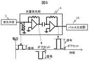
図5は光量受光部6の詳細回路構成を示した図である。
上段に回路図、下段に各位置に対応した電圧を示している。
回路構成は、受光手段3から流れ込む電流を抵抗により電圧に変換し、微小電圧を増幅器62により増幅する。さらにアンプによって生じたオフセット成分をコンデンサで除去し、最後に電圧を増幅し信号をパルス生成部10に出力する構成となっている。
FIG. 5 is a diagram showing a detailed circuit configuration of the light quantity
The upper diagram shows a circuit diagram, and the lower diagram shows the voltage corresponding to each position.
In the circuit configuration, a current flowing from the light receiving means 3 is converted into a voltage by a resistor, and a minute voltage is amplified by an
図6は電流電圧変換部61をアンプを用い構成した図を示している。図5では電流電圧変換部61を抵抗のみで構成しているが、図6のようにアンプを用いて構成してもよい。電流を電圧に変換する手段であればよい。
FIG. 6 shows a diagram in which the current-
増幅部62は帰還抵抗にコンデンサを並列に接続しフィルタとして使用してもよい。またオフセット除去部63はコンデンサのみでなく、抵抗を用いハイパスフィルタを形成してもよい。電流電圧変換部61、増幅部62、オフセット除去部63はそれぞれの機能を満たす構成であれば、フィルタ機能等性能を向上する機能を付加してもよい。
The amplifying
次に回路処理方法により生じる問題点について説明する。
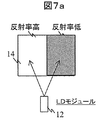
図7aと図7bは回路処理方法により生じる問題点を示した図である。
図7aは同距離で反射率が異なる対象物14にレーザモジュール12から光を照射した図であり、図7bは対象物14から受光手段3に検出される光(以下戻り光)の受光強度を示した図である。
Next, problems caused by the circuit processing method will be described.
7a and 7b are diagrams showing problems caused by the circuit processing method.
FIG. 7a is a diagram in which light is irradiated from the
図7bに示すように、反射率高の波形と反射率低の波形は検出波形が異なるため、基準電圧と比較しパルスを出力する際時間差を生じる。受光強度によるズレに加え、後段で使用するアンプは受光強度によりオフセットレベルが異なるため、さらにパルスのズレを生じる。 As shown in FIG. 7b, a waveform with a high reflectance and a waveform with a low reflectance have different detection waveforms, so that a time difference is generated when a pulse is output compared to a reference voltage. In addition to the shift due to the received light intensity, the amplifier used in the subsequent stage has an offset level that differs depending on the received light intensity, and thus further shifts in the pulse.
つぎに後段のアンプにより生じる問題点を以下に示す。
図8aと図8bは、受光手段3、光量受光部6、パルス生成部10の構成とそれぞれの出力信号の遷移を示した図である。図8aのAは受光手段3の出力、Bは光量受光部6の出力、Cはパルス生成部10の出力を示している。パルス生成部10は入力信号と基準電圧を比較しパルス変換を行う。A,B,C各パルスは、出射開始時は反射率高の面からの戻り光、後半は反射率低の面からの戻り光に対応している。
Next, problems caused by the subsequent amplifier are shown below.
FIGS. 8a and 8b are diagrams showing the configuration of the light receiving means 3, the light amount
ここで反射率低の面からの信号は受光手段3の出力信号として検出されているが、オフセットレベルが変化することでパルス生成部10から出力されない。そのため反射率低の領域で距離測定不能となる場合が生じる。
Here, the signal from the surface with low reflectivity is detected as the output signal of the light receiving means 3, but is not output from the
以上受光手段3の検出波形、強度の相違により、出力パルスにズレを生じるため、受光手段3で光を検出する段階で受光レベルを合わせておく必要がある。例として同距離で反射率が異なる場合を示したが、上記問題はこの場合に限らず光量差がある場合生じる。例えば距離が異なる場合でも光量が異なるため生じる問題である。 As described above, since the output pulse is shifted due to the difference in the detection waveform and intensity of the light receiving means 3, it is necessary to adjust the light receiving level when the light is detected by the light receiving means 3. As an example, the case where the reflectance is different at the same distance has been shown. However, the above problem is not limited to this case, and occurs when there is a light amount difference. For example, even when the distance is different, the problem arises because the light quantity is different.
次に本発明の具体的な駆動方法に関し説明する。説明では受光手段3から取り込んだ信号を微分し、信号の微分値を基にバイアス電圧を制御し受光手段3の受光レベルを調整する方法を記載する。 Next, a specific driving method of the present invention will be described. In the description, a method of differentiating the signal taken from the light receiving means 3 and controlling the bias voltage based on the differential value of the signal to adjust the light receiving level of the light receiving means 3 will be described.
図9はバイアス電圧制御シーケンスを示した図である。ここでは反射角度可変ミラー2を2次元にスキャンし、1フレーム毎にバイアス電圧を制御する場合を例に説明する。
FIG. 9 is a diagram showing a bias voltage control sequence. Here, an example will be described in which the reflection angle
まずバイアス電圧制御シーケンスは、読み込み期間、バイアス電圧制御期間から構成される。読み込み期間では受光手段3の信号を基に算出した値と印加したバイアス電圧の関係から次フレームに印加する目標バイアス電圧をデータとして格納する。バイアス電圧制御期間では、読み込み期間で得た目標バイアス電圧を受光手段3に印加する。 First, the bias voltage control sequence includes a reading period and a bias voltage control period. In the reading period, the target bias voltage to be applied to the next frame is stored as data from the relationship between the value calculated based on the signal of the light receiving means 3 and the applied bias voltage. In the bias voltage control period, the target bias voltage obtained in the reading period is applied to the light receiving means 3.
図10は増幅率制御部の回路構成を示した図である。増幅率制御部7の構成を示した図である。増幅率制御部は微分回路71、目標バイアス算出部72、バイアス電圧生成部73から構成される。受光手段3の出力は微分回路71に入力され、入力波形の微分値を目標バイアス電圧算出部72に出力する。目標バイアス電圧算出部72は微分回路71の出力信号、目標微分値さらにバイアス電圧から目標バイアス電圧生成信号を算出する。目標電圧生成部73はバイアス電圧制御期間に目標バイアス電圧生成信号に応じたバイアス電圧を生成する。
FIG. 10 is a diagram illustrating a circuit configuration of the amplification factor control unit. 6 is a diagram showing a configuration of an amplification factor control unit 7. FIG. The amplification factor control unit includes a
ここで図10における目標微分値をA、バイアス電圧値Vij(n)、目標バイアス電圧Vij(n+1)とする。i,jは解像度を示しており、i列番号、jは行番号,nはフレーム数を示している。つつまりVij(n)はi列j行にレーザを照射する際のnフレーム目のバイアス電圧を示している。目標バイアス電圧算出部72は、入力信号をADコンバータによりデジタル値に変換し、その値を用い目標バイアス電圧生成信号を算出してもよいし、入力信号の最大値のみを使用し算出してもよい。
Here, the target differential value in FIG. 10 is A, the bias voltage value Vij (n), and the target bias voltage Vij (n + 1). i, j indicates the resolution, i column number, j indicates the row number, and n indicates the number of frames. That is, Vij (n) indicates the bias voltage of the nth frame when the laser is irradiated to the i column and the j row. The target bias
図11は読み込み期間及びバイアス電圧制御期間におけるバイアス電圧Vij(n)の制御方法を示した図である。縦列は偶数フレームの読み込み期間、奇数フレームのバイアス電圧制御期間におけるバイアス電圧を示しており、横軸はi列の値を示している。 FIG. 11 is a diagram illustrating a control method of the bias voltage Vij (n) in the reading period and the bias voltage control period. The vertical column indicates the bias voltage during the even frame reading period and the odd frame bias voltage control period, and the horizontal axis indicates the i column value.
まず(n)フレーム目でどの列にも一定のバイアス電圧を印加する。次に(n+1)フレームで(n)フレーム目の印加電圧を基に増幅率制御部7で生成したバイアス電圧を印加する。(n+2)フレーム目の読み込み期間では、一定電圧を使用してもよいし、(n+1)フレームの電圧を使用してもよい。 First, a constant bias voltage is applied to every column in the (n) frame. Next, a bias voltage generated by the amplification factor controller 7 is applied in the (n + 1) frame based on the applied voltage in the (n) frame. In the reading period of the (n + 2) frame, a constant voltage may be used, or a voltage of the (n + 1) frame may be used.
上記実施例ではフレーム毎に制御を行ったが、1フレームおきにバイアス電圧制御期間を設けることは、一点毎のデータを正確に測定でき解像度は高い。しかし2フレームに1回制御を行うため応答速度が半減する。 In the above embodiment, control is performed for each frame. However, providing a bias voltage control period every other frame enables accurate measurement of data for each point and high resolution. However, since the control is performed once every two frames, the response speed is halved.
応答速度が求められるアプリケーションに対してはライン毎、または画素毎に行ってもよい。例えばj行(またはi列)目で読み込んだデータをj+1行(またはi+1列)目にバイアス電圧として印加してもよい。この場合解像度がi*j/2(またはi/2*j)となるが、1フレーム毎に最適なバイアス電圧を印加するため、応答速度を求められるアプリケーションに適している。 For an application for which a response speed is required, it may be performed for each line or for each pixel. For example, data read in the j-th row (or i-th column) may be applied as a bias voltage to the j + 1-th row (or i + 1-th column). In this case, the resolution is i * j / 2 (or i / 2 * j), but since an optimum bias voltage is applied every frame, it is suitable for applications that require a response speed.
本発明の第2の実施例を図12により説明する。本実施例は実施例1と異なり光源1の強度を制御し受光手段3の受光レベルを調整する。
A second embodiment of the present invention will be described with reference to FIG. Unlike the first embodiment, the present embodiment controls the intensity of the
図12は実施例2の構成を示した図である。実施例1と異なる点は、増幅率制御部7の出力であるレーザ強度制御信号104がレーザ光源駆動部5に入力されている点である。以下実施例2における増幅率制御部7の構成を図13により説明する。
FIG. 12 is a diagram showing the configuration of the second embodiment. The difference from the first embodiment is that a laser
図13は実施例2における増幅率制御部7の構成を示した図である。実施例1と異なる点は、レーザ強度制御部74が追加された点である。レーザ強度制御部74は目標バイアス電圧生成信号からレーザ光源駆動部5を動作させる信号を生成する。
FIG. 13 is a diagram showing a configuration of the amplification factor control unit 7 in the second embodiment. The difference from the first embodiment is that a laser
レーザ強度制御部74はレーザ光源駆動部5に付加する信号を送り電流を制御してもよいし、光源1のアノードの印加電圧を制御してもよい。また目標バイアス生成信号に応じた電流をレーザ強度制御部74で生成してもよい。レーザ強度を制御する手段であればよい。
The laser
またレーザ強度を制御する手段だけでなく、同時に受光手段3のバイアス電圧を制御してもよい。受光手段3での受光レベルを調整する手段であれば複数の手段を用いてもよい。 In addition to the means for controlling the laser intensity, the bias voltage of the light receiving means 3 may be controlled simultaneously. A plurality of means may be used as long as the light receiving level at the light receiving means 3 is adjusted.
上述の実施例では受光手段3がAPDの場合について記述したが、外部より受光手段の増幅率、言い換えれば、受光手段3は感度を調整できる受光センサであればよく、APDに限定されるものではない。 In the above-described embodiment, the case where the light receiving means 3 is an APD has been described. However, the gain of the light receiving means from the outside, in other words, the light receiving means 3 may be any light receiving sensor capable of adjusting the sensitivity, and is not limited to the APD. Absent.
1 レーザ光源
2 反射角度可変ミラー
3 受光手段
4 ミラー駆動部
5 レーザ光源駆動部
6 光量受光部
7 増幅率制御部
8 同期信号生成部
9 制御信号生成部
10 パルス生成部
11 距離算出部
12 レーザモジュール
13 駆動基板
14 対象物
61 電流電圧変換部
62 増幅部
63 オフセット除去部
71 微分回路
72 目標バイアス電圧算出部
73 バイアス電圧生成部
74 レーザ強度制御部
100ミラー駆動部制御信号
100レーザ光源駆動部制御信号
102バイアス電圧制御信号
103レーザパルス出射タイミング信号
104レーザ制御信号
200同期信号
203レーザ駆動信号
201水平方向駆動信号
202垂直駆動信号
1 Laser light source
2 Variable reflection angle mirror
3 Light receiving means
4 Mirror drive unit
5 Laser light source driver
6 Light receiver
7 Gain control section
8 Sync signal generator
9 Control signal generator
10 Pulse generator
11 Distance calculator
12 Laser module
13 Drive board
14 Object
61 Current-voltage converter
62 Amplifier
63 Offset remover
71 Differentiation circuit
72 Target bias voltage calculator
73 Bias voltage generator
74 Laser intensity controller
100 mirror drive control signal
100 Laser light source driver control signal
102 Bias voltage control signal
103 Laser pulse emission timing signal
104 Laser control signal
200 sync signal
203 Laser drive signal
201 Horizontal drive signal
202 vertical drive signal
Claims (8)
前記測距光を発光する光源と、
前記測定対象物に前記測距光を走査する反射角度可変ミラーと、
前記測距光の前記測定対象物からの前記反射光を受光し、該反射光の強度或いは光量に応じた信号を出力する受光手段と、
前記受光手段からの出力信号を増幅する増幅部と、
前記受光手段からの前記出力信号に基づいて前記受光手段の受光感度を制御するための目標バイアス電圧を生成する増幅率制御部と、
前記増幅部からの出力信号に基づいて前記測距光の飛行時間を検出し、前記測定対象物までの距離を算出する距離算出部と、を備え、
第1の走査期間に、前記増幅率制御部は前記受光手段からの前記出力信号に基づいて前記目標バイアス電圧を生成し、
第2の走査期間に、前記増幅率制御部は前記受光手段の前記受光感度を前記第1の走査期間で生成した前記目標バイアス電圧により制御し、前記距離算出部が前記測定対象物までの距離を算出し、
前記増幅率制御部は、前記受光手段により得られた前記出力信号を微分する微分回路を含み、更に、該微分回路からの出力信号に基づいて前記目標バイアス電圧を生成する、
光測距装置。 An optical distance measuring device that irradiates a measuring object with a ranging light, receives a reflected light from the measuring object, and measures a distance to the measuring object,
A light source that emits the distance measuring light;
A reflection angle variable mirror that scans the distance measuring light on the measurement object;
A light receiving means for receiving the reflected light from the measurement object of the distance measuring light and outputting a signal corresponding to the intensity or the amount of the reflected light ;
An amplifier for amplifying an output signal from the light receiving means;
A gain controller for generating a target bias voltage for controlling the light sensitivity of the light receiving means based on the said output signal from said light receiving means,
A distance calculation unit that detects a flight time of the ranging light based on an output signal from the amplification unit, and calculates a distance to the measurement object;
In the first scanning period, the amplification factor controller generates the target bias voltage based on the output signal from the light receiving means ,
In the second scanning period, the amplification factor control unit controls the light receiving sensitivity of the light receiving means by the target bias voltage generated in the first scanning period, and the distance calculation unit measures the distance to the measurement object. is calculated,
The amplification factor control unit includes a differentiating circuit that differentiates the output signal obtained by the light receiving means, and further generates the target bias voltage based on an output signal from the differentiating circuit.
Optical distance measuring device.
前記反射角度可変ミラーは2次元に前記測距光を走査し、
前記第1の走査期間と前記第2の走査期間は、前記2次元の走査フレームごとに切り替える、
光測距装置。 The optical distance measuring device according to claim 1,
The reflection angle variable mirror scans the distance measuring light in two dimensions,
The first scanning period and the second scanning period are switched for each of the two-dimensional scanning frames.
Optical distance measuring device.
前記反射角度可変ミラーは2次元に前記測距光を走査し、
前記第1の走査期間と前記第2の走査期間は、前記2次元の走査フレームの所定の解像度ごとに切り替える、
光測距装置。 The optical distance measuring device according to claim 1,
The reflection angle variable mirror scans the distance measuring light in two dimensions,
The first scanning period and the second scanning period are switched for each predetermined resolution of the two-dimensional scanning frame.
Optical distance measuring device.
前記反射角度可変ミラーは1次元に前記測距光を走査し、
前記第1の走査期間と前記第2の走査期間は、前記1次元の走査フレームごとに切り替える、
光測距装置。 The optical distance measuring device according to claim 1,
The reflection angle variable mirror scans the distance measuring light in one dimension,
The first scanning period and the second scanning period are switched for each one-dimensional scanning frame.
Optical distance measuring device.
前記反射角度可変ミラーは1次元に前記測距光を走査し、
前記第1の走査期間と前記第2の走査期間は、前記1次元の走査フレームの所定の解像度ごとに切り替える、
光測距装置。 The optical distance measuring device according to claim 1,
The reflection angle variable mirror scans the distance measuring light in one dimension,
The first scanning period and the second scanning period are switched for each predetermined resolution of the one-dimensional scanning frame.
Optical distance measuring device.
前記出力信号のオフセット成分を除去するオフセット除去部を含む、
光測距装置。 In the optical ranging apparatus in any one of Claim 1 to 5,
An offset removing unit for removing an offset component of the output signal ;
Optical distance measuring device.
前記受光手段はアバランシェフォトダイオードである、
光測距装置。 The optical distance measuring device according to any one of claims 1 to 6 ,
The light receiving means is an avalanche photodiode;
Optical distance measuring device.
前記光源はレーザである、
光測距装置。 The optical distance measuring device according to any one of claims 1 to 6 ,
The light source is a laser;
Optical distance measuring device.
Priority Applications (4)
| Application Number | Priority Date | Filing Date | Title |
|---|---|---|---|
| JP2013079114A JP6045963B2 (en) | 2013-04-05 | 2013-04-05 | Optical distance measuring device |
| EP14163155.6A EP2787368B1 (en) | 2013-04-05 | 2014-04-02 | Optical distance measuring apparatus |
| US14/242,908 US9696425B2 (en) | 2013-04-05 | 2014-04-02 | Optical distance measuring apparatus |
| CN201410133953.5A CN104101880B (en) | 2013-04-05 | 2014-04-03 | Optical distance measuring apparatus |
Applications Claiming Priority (1)
| Application Number | Priority Date | Filing Date | Title |
|---|---|---|---|
| JP2013079114A JP6045963B2 (en) | 2013-04-05 | 2013-04-05 | Optical distance measuring device |
Publications (3)
| Publication Number | Publication Date |
|---|---|
| JP2014202610A JP2014202610A (en) | 2014-10-27 |
| JP2014202610A5 JP2014202610A5 (en) | 2015-11-12 |
| JP6045963B2 true JP6045963B2 (en) | 2016-12-14 |
Family
ID=50391102
Family Applications (1)
| Application Number | Title | Priority Date | Filing Date |
|---|---|---|---|
| JP2013079114A Active JP6045963B2 (en) | 2013-04-05 | 2013-04-05 | Optical distance measuring device |
Country Status (4)
| Country | Link |
|---|---|
| US (1) | US9696425B2 (en) |
| EP (1) | EP2787368B1 (en) |
| JP (1) | JP6045963B2 (en) |
| CN (1) | CN104101880B (en) |
Families Citing this family (27)
| Publication number | Priority date | Publication date | Assignee | Title |
|---|---|---|---|---|
| US9510505B2 (en) * | 2014-10-10 | 2016-12-06 | Irobot Corporation | Autonomous robot localization |
| JP2016170114A (en) * | 2015-03-13 | 2016-09-23 | 株式会社東芝 | Distance measuring device and photodetector |
| CN106291568A (en) * | 2015-05-27 | 2017-01-04 | 上海诺司纬光电仪器有限公司 | Improve the system and method for accuracy of laser distance measuring instrument |
| JP6557516B2 (en) | 2015-06-04 | 2019-08-07 | 株式会社トプコン | 3D surveying apparatus and 3D surveying method |
| WO2016199267A1 (en) * | 2015-06-11 | 2016-12-15 | 日立マクセル株式会社 | Optical distance measurement device, control method therefor, and gesture detection device using same |
| EP3356845B1 (en) * | 2015-09-30 | 2019-11-20 | Trimble AB | Geodetic instrument with improved dynamic range |
| WO2017060943A1 (en) * | 2015-10-05 | 2017-04-13 | 日立マクセル株式会社 | Optical ranging device and image projection apparatus |
| JP2017150893A (en) * | 2016-02-23 | 2017-08-31 | ソニー株式会社 | Ranging module, ranging system, and control method of ranging module |
| KR20180014617A (en) * | 2016-08-01 | 2018-02-09 | 엘지전자 주식회사 | Asymmetry optical sensor apparatus |
| JP2018031607A (en) * | 2016-08-23 | 2018-03-01 | ソニーセミコンダクタソリューションズ株式会社 | Distance measuring device, electronic device, and method for controlling distance measuring device |
| JP6732634B2 (en) * | 2016-11-08 | 2020-07-29 | 株式会社東芝 | Distance measuring device |
| JP6775119B2 (en) * | 2017-03-23 | 2020-10-28 | パナソニックIpマネジメント株式会社 | Distance measuring device |
| JP6743761B2 (en) * | 2017-05-29 | 2020-08-19 | 株式会社デンソー | Ranging sensor |
| KR102506438B1 (en) * | 2017-07-06 | 2023-03-06 | 삼성전자주식회사 | Distance measuring device and method for measuring distance by using thereof |
| JP2019028013A (en) * | 2017-08-03 | 2019-02-21 | オムロンオートモーティブエレクトロニクス株式会社 | Object detection device |
| CN107566065A (en) * | 2017-08-25 | 2018-01-09 | 中山大学深圳研究院 | TOF localization methods based on UWB |
| WO2019044487A1 (en) * | 2017-08-28 | 2019-03-07 | ソニーセミコンダクタソリューションズ株式会社 | Distance measuring device and distance measuring method |
| KR102429879B1 (en) * | 2017-09-13 | 2022-08-05 | 삼성전자주식회사 | LiDAR apparatus and method of operating LiDAR apparatus |
| CN112105955A (en) * | 2018-04-09 | 2020-12-18 | 感应光子公司 | LIDAR automatic gain control for autonomous vehicles |
| JP7178819B2 (en) * | 2018-07-18 | 2022-11-28 | 浜松ホトニクス株式会社 | Semiconductor photodetector |
| JP6990356B2 (en) * | 2018-10-30 | 2022-01-12 | オムロン株式会社 | Sensor device and detection method |
| JP2020076653A (en) * | 2018-11-08 | 2020-05-21 | オムロン株式会社 | Optical measuring device and optical measuring method |
| JP7337517B2 (en) * | 2019-03-14 | 2023-09-04 | 株式会社東芝 | Photodetector and distance measuring device |
| CN110127478B (en) * | 2019-04-02 | 2020-10-23 | 日立楼宇技术(广州)有限公司 | Method and device for determining position of elevator car and elevator distance measuring system |
| CN110471072B (en) * | 2019-08-19 | 2021-04-02 | 华晟(青岛)智能装备科技有限公司 | Method and system for identifying position of reflecting column |
| JP2021173978A (en) * | 2020-04-30 | 2021-11-01 | キヤノン株式会社 | Image forming apparatus |
| EP4212907A4 (en) | 2020-10-14 | 2023-11-01 | NEC Corporation | Optical distance measurement device and optical distance measurement method |
Family Cites Families (14)
| Publication number | Priority date | Publication date | Assignee | Title |
|---|---|---|---|---|
| JPH0562883U (en) * | 1992-01-30 | 1993-08-20 | 株式会社ニコン | Distance measuring device |
| JP3042278B2 (en) * | 1993-09-17 | 2000-05-15 | 三菱電機株式会社 | Distance measuring device |
| JP4630413B2 (en) * | 1999-12-07 | 2011-02-09 | 株式会社トプコン | Distance measuring machine and light receiving unit adjusting method of distance measuring machine |
| FR2817339B1 (en) * | 2000-11-24 | 2004-05-14 | Mensi | THREE-DIMENSIONAL LIFTING DEVICE OF A LASER EMISSION SCENE |
| EP1842082A2 (en) * | 2005-01-20 | 2007-10-10 | Elbit Systems Electro-Optics Elop Ltd. | Laser obstacle detection and display |
| JP4979916B2 (en) * | 2005-09-12 | 2012-07-18 | 株式会社トプコン | Surveying device and surveying method |
| JP4898176B2 (en) * | 2005-09-26 | 2012-03-14 | 株式会社トプコン | Surveying device and surveying method |
| JP4888065B2 (en) * | 2005-12-08 | 2012-02-29 | オムロン株式会社 | Laser scanning device |
| JP5173017B2 (en) * | 2008-03-20 | 2013-03-27 | トリムブレ、アクチボラグ | Efficient geodetic scanner |
| JP5723517B2 (en) | 2009-06-15 | 2015-05-27 | 日本信号株式会社 | Optical distance measuring device |
| WO2010149219A1 (en) * | 2009-06-26 | 2010-12-29 | Trimble Ab | Distance measuring device |
| JP2011089874A (en) * | 2009-10-22 | 2011-05-06 | Toyota Central R&D Labs Inc | Distance image data acquisition device |
| JP5516145B2 (en) | 2010-06-30 | 2014-06-11 | セイコーエプソン株式会社 | Optical detection device, display device, and electronic apparatus |
| JP5711925B2 (en) * | 2010-09-22 | 2015-05-07 | 日本信号株式会社 | Optical distance measuring device |
-
2013
- 2013-04-05 JP JP2013079114A patent/JP6045963B2/en active Active
-
2014
- 2014-04-02 EP EP14163155.6A patent/EP2787368B1/en active Active
- 2014-04-02 US US14/242,908 patent/US9696425B2/en active Active
- 2014-04-03 CN CN201410133953.5A patent/CN104101880B/en active Active
Also Published As
| Publication number | Publication date |
|---|---|
| US20140300887A1 (en) | 2014-10-09 |
| EP2787368B1 (en) | 2020-02-12 |
| JP2014202610A (en) | 2014-10-27 |
| EP2787368A1 (en) | 2014-10-08 |
| CN104101880B (en) | 2017-05-17 |
| CN104101880A (en) | 2014-10-15 |
| US9696425B2 (en) | 2017-07-04 |
Similar Documents
| Publication | Publication Date | Title |
|---|---|---|
| JP6045963B2 (en) | Optical distance measuring device | |
| JP6633197B2 (en) | Photodetector and electronic equipment | |
| AU2019268121B2 (en) | LiDAR scanner calibration | |
| US20170082746A1 (en) | Distance measuring device | |
| CN109521435B (en) | Distance measuring device | |
| US7630062B2 (en) | Distance measuring apparatus | |
| JP6933473B2 (en) | Distance measuring device and distance imaging device | |
| JP2021107832A (en) | Distance measuring device | |
| JP2019052978A (en) | Distance measuring device | |
| JP4837413B2 (en) | Ranging method and ranging device | |
| KR20160092137A (en) | Controlling method in distance measuring device using TOF | |
| US11525913B2 (en) | Light detection device and electronic apparatus comprising plural SPAD arrays with a photon detection rate controller | |
| US11391824B2 (en) | Distance measuring device and distance measuring method | |
| JP5391127B2 (en) | Time measuring device and distance measuring device | |
| JP2019158604A (en) | Light detection device, light detection method and lidar device | |
| JP7303671B2 (en) | Electronic device and distance measurement method | |
| JP7253846B2 (en) | Range image sensor and range image pickup device | |
| JP5191107B2 (en) | Ranging device | |
| JP2007212157A (en) | Optical range finder | |
| JP2001050711A (en) | Optical displacement meter |
Legal Events
| Date | Code | Title | Description |
|---|---|---|---|
| A711 | Notification of change in applicant |
Free format text: JAPANESE INTERMEDIATE CODE: A712 Effective date: 20140917 |
|
| A521 | Request for written amendment filed |
Free format text: JAPANESE INTERMEDIATE CODE: A523 Effective date: 20150925 |
|
| A621 | Written request for application examination |
Free format text: JAPANESE INTERMEDIATE CODE: A621 Effective date: 20150925 |
|
| A131 | Notification of reasons for refusal |
Free format text: JAPANESE INTERMEDIATE CODE: A131 Effective date: 20160830 |
|
| A977 | Report on retrieval |
Free format text: JAPANESE INTERMEDIATE CODE: A971007 Effective date: 20160831 |
|
| A521 | Request for written amendment filed |
Free format text: JAPANESE INTERMEDIATE CODE: A523 Effective date: 20161021 |
|
| TRDD | Decision of grant or rejection written | ||
| A01 | Written decision to grant a patent or to grant a registration (utility model) |
Free format text: JAPANESE INTERMEDIATE CODE: A01 Effective date: 20161108 |
|
| A61 | First payment of annual fees (during grant procedure) |
Free format text: JAPANESE INTERMEDIATE CODE: A61 Effective date: 20161116 |
|
| R150 | Certificate of patent or registration of utility model |
Ref document number: 6045963 Country of ref document: JP Free format text: JAPANESE INTERMEDIATE CODE: R150 |
|
| S111 | Request for change of ownership or part of ownership |
Free format text: JAPANESE INTERMEDIATE CODE: R313111 |
|
| R350 | Written notification of registration of transfer |
Free format text: JAPANESE INTERMEDIATE CODE: R350 |
|
| R250 | Receipt of annual fees |
Free format text: JAPANESE INTERMEDIATE CODE: R250 |
|
| R250 | Receipt of annual fees |
Free format text: JAPANESE INTERMEDIATE CODE: R250 |
|
| S111 | Request for change of ownership or part of ownership |
Free format text: JAPANESE INTERMEDIATE CODE: R313111 |
|
| R250 | Receipt of annual fees |
Free format text: JAPANESE INTERMEDIATE CODE: R250 |
|
| R350 | Written notification of registration of transfer |
Free format text: JAPANESE INTERMEDIATE CODE: R350 |
|
| R250 | Receipt of annual fees |
Free format text: JAPANESE INTERMEDIATE CODE: R250 |
|
| R250 | Receipt of annual fees |
Free format text: JAPANESE INTERMEDIATE CODE: R250 |