WO2024024697A1 - マイクロ流体デバイス、マイクロ流体デバイスの観察装置、マイクロ流体デバイスの観察方法 - Google Patents
マイクロ流体デバイス、マイクロ流体デバイスの観察装置、マイクロ流体デバイスの観察方法 Download PDFInfo
- Publication number
- WO2024024697A1 WO2024024697A1 PCT/JP2023/026894 JP2023026894W WO2024024697A1 WO 2024024697 A1 WO2024024697 A1 WO 2024024697A1 JP 2023026894 W JP2023026894 W JP 2023026894W WO 2024024697 A1 WO2024024697 A1 WO 2024024697A1
- Authority
- WO
- WIPO (PCT)
- Prior art keywords
- microfluidic device
- observation
- optically transparent
- transparent portion
- light
- Prior art date
- Legal status (The legal status is an assumption and is not a legal conclusion. Google has not performed a legal analysis and makes no representation as to the accuracy of the status listed.)
- Ceased
Links
Images





Classifications
-
- G—PHYSICS
- G01—MEASURING; TESTING
- G01N—INVESTIGATING OR ANALYSING MATERIALS BY DETERMINING THEIR CHEMICAL OR PHYSICAL PROPERTIES
- G01N21/00—Investigating or analysing materials by the use of optical means, i.e. using sub-millimetre waves, infrared, visible or ultraviolet light
- G01N21/01—Arrangements or apparatus for facilitating the optical investigation
- G01N21/03—Cuvette constructions
-
- G—PHYSICS
- G01—MEASURING; TESTING
- G01N—INVESTIGATING OR ANALYSING MATERIALS BY DETERMINING THEIR CHEMICAL OR PHYSICAL PROPERTIES
- G01N21/00—Investigating or analysing materials by the use of optical means, i.e. using sub-millimetre waves, infrared, visible or ultraviolet light
- G01N21/62—Systems in which the material investigated is excited whereby it emits light or causes a change in wavelength of the incident light
- G01N21/63—Systems in which the material investigated is excited whereby it emits light or causes a change in wavelength of the incident light optically excited
- G01N21/64—Fluorescence; Phosphorescence
Definitions
- the present invention relates to a microfluidic device, a microfluidic device observation apparatus, and a microfluidic device observation method.
- Patent Document 1 describes a microfluidic device observation apparatus and a microfluidic device observation method for observing a specimen existing inside the channels of a microfluidic device in which one or more channels are arranged. Are listed. [Prior art documents] [Patent document] [Patent Document 1] International Publication No. 2020/021604 [General Disclosure]
- a microfluidic device having a top surface, a bottom surface, and a plurality of side surfaces, wherein at least one of the plurality of side surfaces is an optical device that transmits illumination light from the outside.
- a microfluidic device is provided having a permeable portion.
- the optically transparent portion may be formed corresponding to an observation area to be observed.
- a plurality of the optically transparent parts may be formed on the at least one side surface.
- the one side surface may include a marker for searching or specifying the position of the optically transparent portion.
- the optically transparent portion may have an optical function.
- the optical function may be a convex lens function.
- the optical function may be a concave lens function.
- the optical function may be a function of separating the illumination light into multiple directions.
- a mask may be formed on the optically transparent portion to block part of the illumination light.
- the optically transparent portion may have a mark formed corresponding to an observation area to be observed.
- At least one of the top surface and the bottom surface may have an optically transparent portion that transmits output light output from within the microfluidic device.
- an observation apparatus for a microfluidic device which has a top surface, a bottom surface, and a plurality of side surfaces, and at least one of the plurality of side surfaces receives illumination light from the outside.
- An illumination optical system that illuminates illumination light from the optically transparent portion, and an observation optical system that receives output light from at least one of the top surface and the bottom surface, are provided for a microfluidic device having an optically transparent portion that transmits the microfluidic device.
- an observation apparatus for a microfluidic device is provided.
- the angle of incidence of the illumination light onto the optically transparent portion may be variable.
- the one side may include a marker for searching or specifying the position of the optically transparent portion, and may include a marker observation optical system for observing the marker, and a light source for irradiating the marker with illumination light. It may further include.
- control device may control the illumination optical system to form the illumination light based on information regarding the observation area corresponding to the optically transparent portion.
- a method for observing a microfluidic device which has a top surface, a bottom surface, and a plurality of side surfaces, and at least one of the plurality of side surfaces is illuminated by external illumination light.
- a microfluidic device having an optically transparent portion that transmits the microfluidic device, an illumination stage that illuminates the illumination light from the optically transparent portion, and an observation stage that receives output light from at least one of the top surface and the bottom surface;
- a method for observing a microfluidic device is provided.
- the angle of incidence of the illumination light onto the optically transparent portion may be variable.
- FIG. 1 is a perspective view showing an example of a schematic configuration of a microfluidic device 100 in a first embodiment.
- FIG. 1 is a side view showing an example of a schematic configuration of a microfluidic device 100 in a first embodiment.
- An example of a schematic configuration of an observation device 200 of a microfluidic device 100 in the first embodiment is shown.
- FIG. 3 is an explanatory diagram of angle adjustment of sheet light L1 of the microfluidic device 100 in the first embodiment. It is a flowchart showing the operation of the observation device 200 of the microfluidic device 100 in the first embodiment.
- FIG. 2 is a perspective view showing an example of a schematic configuration of a microfluidic device 110 in a second embodiment.
- FIG. 3 is a side view showing an example of a schematic configuration of a microfluidic device 110 in a second embodiment.
- An example of a schematic configuration of an observation device 270 of the microfluidic device 110 in the second embodiment is shown. It is a flowchart showing the operation of the observation device 270 of the microfluidic device 110 in the second embodiment.
- a transmission window 131 in a first modification is shown.
- a transmission window 141 in a second modification is shown.
- a transmission window 151 in a third modification is shown.
- a transmission window 161 in a fourth modification is shown. It is a figure which shows the modification of an illumination method.
- An example of a computer 2200 is shown.
- FIG. 1 is a perspective view showing an example of a schematic configuration of a microfluidic device 100 in the first embodiment.
- microfluidic devices 100 have a top surface 100a, a bottom surface 100b, and four side surfaces 100c to 100f.
- the top surface 100a is a surface facing in the direction opposite to the direction of gravity when the microfluidic device 100 is placed for observation
- the bottom surface 100b is a surface facing in the direction opposite to the direction of gravity when the microfluidic device 100 is placed for observation.
- the side facing The four side surfaces 100c to 100f are surfaces perpendicular to the top surface 100a and the bottom surface 100b.
- the side surface 100c is a side surface of the microfluidic device 100 facing in the -X direction
- the side surface 100d is a side surface facing the +Y direction of the microfluidic device 100
- the side surface 100e is a side surface facing the +X direction of the microfluidic device 100.
- the side face 100f is the side face of the microfluidic device 100 facing in the -Y direction.
- the microfluidic device 100 has a plurality of layers, and each layer of the microfluidic device 100 has a plurality of structures 101 such as microchannels and injection ports through which cells can be injected.
- the microfluidic device 100 has a substantially rectangular parallelepiped shape, but the present invention is also applicable to microfluidic devices having other three-dimensional shapes.
- the microfluidic device 100 has a transmission surface 102 on which at least one of the plurality of sides is an optically transparent portion that transmits illumination light from the outside.
- the illumination light is, for example, excitation light in the visible or infrared region for fluorescence observation, and illumination light in the visible region for observation by transmission or reflection.
- the top surface 101a or bottom surface 100b of the microfluidic device 100 has an optically transparent portion that transmits observation light.
- the observation light is, for example, fluorescence in the visible range for fluorescence observation, and observation light in the visible range for observation by transmission or reflection.
- the microfluidic device 100 is a microfluidic device in which samples corresponding to minute biological substances such as DNA, proteins, cells, cell masses (spheroids, organoids, etc.), tissues, etc. are placed on a small substrate to detect genetic defects, protein distribution, and reactions.
- the microfluidic device 100 in this embodiment includes an organ chip (organ on a chip), a biological function chip (organ on a chip), an MPS (microphysical systems), a biochip (biochip), a microfluidic chip (mic rofluidic chip) , microchip, cell culture chip, microchannel chip, etc.
- the microfluidic device 100 is used, for example, for culturing and analyzing cells and tissues. Furthermore, chemical substances (drugs) are added to the mixture and used for reaction evaluation or analysis with cultured cells.
- the microfluidic device 100 may include both a device in which organ cells are cultured to express a biological function and an "empty" device body in which organ cells are not yet cultured.
- the microfluidic device 100 can be manufactured using, for example, stereolithography three-dimensional printing technology and a solution cast molding process. In addition to the above techniques, the microfluidic device 100 can be manufactured using other microfabrication techniques such as MEMS (Micro Electro Mechanical Systems).
- MEMS Micro Electro Mechanical Systems
- Each layer of the microfluidic device 100 is composed of, for example, a substrate.
- the substrate may be made of glass, for example.
- the substrate may be made of a resin material such as polymethyl methacrylate (PMMA), polycarbonate (PC), cycloolefin copolymer (COC), cycloolefin polymer (COP), polystyrene (PS), silicone, or the like.
- Microfluidic device 100 may have a cover that covers the entire microfluidic device 100.
- FIG. 2 is a side view showing an example of a schematic configuration of the microfluidic device 100 in the first embodiment.
- FIG. 2 is a diagram of the microfluidic device 100 in FIG. 1 viewed from the ⁇ X direction, and shows a side surface 100c of the microfluidic device 100.
- the entire side surface 100c is a transmitting surface 102 that transmits illumination light from the outside.
- External illumination light is light that illuminates the microfluidic device 100 to illuminate the microfluidic device 100 when observing the microfluidic device 100 with an observation device such as a microscope. Therefore, the transmission surface 102 transmits illumination light from the outside.
- the transmitting surface 102 is made of a material that transmits illumination light from the outside, and is made of glass, for example.
- the side surface 100c which is the transmission surface 102, may have a mark formed corresponding to an observation area to be observed. For example, although not shown in FIG. 2, if there is an observation area 300 as shown in FIG. may be formed. This facilitates searching and specifying the position of the observation area.
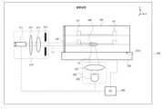
- FIG. 3 shows an example of a schematic configuration of the observation device 200 of the microfluidic device 100 in the first embodiment.
- the observation device 200 in this embodiment is an inverted microscope, for example. However, an upright microscope is also applicable.
- the observation device 200 acquires an image of the observation device 200 by illuminating the microfluidic device 100 with sheet light L1, which is excitation light, and capturing fluorescence excited from the fluorescent dye of the observation device 200.
- the sheet light L1 is illumination light having a sheet-shaped illumination area.
- the observation device 200 includes a sheet illumination optical system 210, an observation optical system 220, a stage 230, and a PC (control device) 240.
- the microfluidic device 100 is arranged on a stage 230 of the observation apparatus 200, and by moving the stage 230 in the vertical direction and the horizontal direction (XYZ direction), the microfluidic device 100 is moved in the vertical direction and the horizontal direction (XYZ direction). It is movable.
- the sheet illumination optical system 210, observation optical system 220, and stage 230 are connected to the PC 240 and can be automatically controlled.
- the sheet illumination optical system 210 includes an optical fiber 211 that propagates laser light emitted from a laser light source (not shown), a collector lens 212, a cylindrical lens 213, and a variable aperture 214.
- the sheet illumination optical system 210 is an illumination optical system that illuminates cells and the like inside the microfluidic device 100.
- the sheet illumination optical system 210 is arranged on the -X direction side of the side surface of the microfluidic device 100, and illuminates the sheet light L1 toward the microfluidic device 100.
- the output end face of the optical fiber 211 which is a component of the sheet illumination optical system 210, constitutes a point light source and is irradiated with laser light.
- the laser light is shaped into a sheet light L1 having a sheet-like shape by the cylindrical lens 213, and the sheet light is limited by the variable aperture 214 and illuminated toward the observation region 300 of the microfluidic device 100.
- the sheet light L1 has a longitudinal direction in a direction perpendicular to the optical axis of the sheet illumination optical system 210.
- the observation area 300 is an area of the microfluidic device 100 that the user wants to observe with a microscope.
- the sheet light L1 enters the inside of the microfluidic device 100 from the side surface 100c of the microfluidic device 100 and illuminates cells and the like inside the microfluidic device 100.
- sheet light L1 is illuminated toward the microfluidic device 100 in parallel to the X axis.
- the output end of the optical fiber 211 is configured to be movable (shiftable) in the height direction ( ⁇ Z direction) from the optical axis of the sheet illumination optical system 210.
- the illumination area of the sheet light L1 can be configured to be movable in the height direction ( ⁇ Z direction). It is desirable that the intensity and longitudinal width of the sheet light L1 be automatically finely adjusted so as to minimize ghosts caused by diffused reflection on the structures 101 inside the microfluidic device 100.
- the observation optical system 220 includes an objective lens 221, a second objective lens (imaging lens) not shown, and a two-dimensional detector 222.
- the objective lens 221 may have a configuration in which low magnification/medium/high magnification can be electrically switched.
- the sheet light L1 emitted from the sheet illumination optical system 210 illuminates cells in the observation region 300 of the microfluidic device 100.
- the observation area 300 is not limited to cells, and may include cell clusters and tissues.
- the cells in the observation area 300 are excited by the sheet light L1 and emit fluorescence L2 as output light. Fluorescence L2 is emitted from the bottom surface 100b of the microfluidic device 100.
- the bottom surface 100b of the microfluidic device 100 is made of a material that transmits the fluorescence L2. Note that the observation may be performed from the direction of the top surface 100a of the microfluidic device 100, in which case the observation optical system 220 is arranged in the direction of the top surface 100a of the microfluidic device 100, and the top surface 100a is made of a material that transmits the fluorescence L2. .
- the fluorescence L2 emitted from the bottom surface 100b of the microfluidic device 100 is focused by the objective lens 221 and detected by the two-dimensional detector 222.
- the two-dimensional detector 222 is, for example, an image sensor such as a CCD (Charge Coupled Device) image sensor or an sCMOS (Scientific Complementary Metal Oxide Semiconductor) image sensor.
- the observation optical system 220 may further include other optical members such as a condenser lens and a dichroic mirror.
- the PC (control device) 240 includes a CPU and a memory (storage unit), and the CPU controls the operation of the observation device 200 by reading and executing a control program stored in the memory. As shown by the dashed line in FIG. 3, the PC 240 is connected to the stage 230 of the microscope, etc., and can control the operation of the entire microscope.
- the PC 240 includes an input unit that receives various instructions and settings from the user and sends them to the control unit of the PC 240, and a GUI (Graphical User Interface) screen and a It has a display section that displays various dialogs and the like.
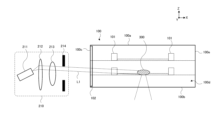
- FIG. 4 is an explanatory diagram of the angle adjustment of the sheet light L1 of the microfluidic device 100 in the first embodiment.
- FIG. 4 is a partially enlarged view of the observation device 200, and only some of the components of the observation device 200 are illustrated.
- the sheet light L1 entering the microfluidic device 100 from the sheet illumination optical system 210 was parallel to the X axis.
- the output end of the optical fiber 211 faces diagonally upward, and the sheet light L1 illuminates the observation area 300 at a diagonally downward angle by passing through the collector lens 212 and the cylindrical lens 213. ing.
- the observation area 300 can be illuminated from an appropriate angle, for example.
- the observation area 300 can be illuminated while avoiding the obstacle. Adjustment of the direction (tilt) of the output end of the optical fiber 211 and adjustment of the height position (shift) (position in the Z direction) of the output end of the optical fiber 211 can be performed in combination.
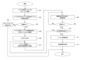
- FIG. 5 is a flowchart showing the operation of the observation apparatus 200 of the microfluidic device 100 in the first embodiment.
- step S01 the user places the microfluidic device 100 on the stage 230 of the microscope.
- step S02 the user selects the type of microfluidic device 100 on the GUI.
- step S03 based on the type of microfluidic device 100 selected by the user, the PC 240 determines whether or not it has information on the microfluidic device 100 of the selected type.
- the information on the microfluidic device 100 provides at least one of the shape, structure, size, manufacturer, cultured cell information, and model number of the microfluidic device 100, for example. If the PC 240 has information on the microfluidic device 100 (step S03: YES), the process advances to step S05, reads out the information on the microfluidic device 100, and allows the user to select the relevant one from among multiple assays displayed on the GUI. Select an assay that is compatible with microfluidic device 100.
- step S03 If the PC 240 does not have information about the microfluidic device 100 (step S03: NO), the process proceeds to step S04, and an error message indicating that the microfluidic device 100 is an incompatible microfluidic device is displayed on the GUI.
- An assay is an image acquisition and analysis routine that obtains a predetermined result by acquiring an image and performing predetermined analysis and evaluation processing on the obtained cell image. There are calculations, cell viability determination, etc.
- step S06 when the user presses the GO button on the GUI, the process proceeds to step S07, where the observation device 200 moves the stage 230 and moves the field of view of the objective lens 221 to the first observation area 300.
- the position of the observation area 300 can be specified by the user with respect to the three-dimensional image of the entire microfluidic device 100 displayed on the GUI, and based on the specified position, the process of step S07 is performed by the observation apparatus 200. done automatically.
- the process in step S07 may be performed manually by the user.
- step S08 the observation conditions (including illumination conditions, magnification of the objective lens 221, relative position between the objective lens 221 and the observation area 300, etc.) are changed in order to acquire an image of the observation area 300, and the observation area 300 is Get the image of.
- the user refers to the three-dimensional image of the entire microfluidic device 100 displayed on the GUI, takes into consideration the structure 101, and selects the optimal transmission window for the first observation area 300. Set the lighting conditions and irradiate the sheet light. Note that by linking information regarding the observation area 300, information regarding the structure 101, and information regarding the transmission window and storing it in the PC 240, the user can perform the first observation simply by specifying the observation area 300.
- the transmission window corresponding to the region 300 may be irradiated with sheet light under optimal illumination conditions.
- the illumination conditions include, for example, the intensity of the sheet light, the width in the longitudinal direction of the sheet light, the illumination position, the illumination angle, the illumination wavelength, the size of a variable aperture corresponding to the longitudinal width of the sheet light, and the like.
- step S09 it is confirmed whether the image quality of the acquired image of the observation area 300 is good, and if it is good (step S09: YES), the process proceeds to the next step S10. If the image quality is not good (step S09: NO), the process returns to step S08 and the observation conditions are reset.
- step S10 it is determined whether there is a next observation area. If there is another observation area (step S10: YES), the process returns to step S07 and the processes from steps S07 to S09 are repeated. If there is no next observation area (step S10: NO), the process proceeds to the next steps S11 and S12.
- step S11 assay image processing (image analysis) is performed, and in step S12, the processing results (analysis results) are saved.
- the side surface 100c of the microfluidic device 100 has the transmission surface 102, which is an optically transparent portion that transmits illumination light from the outside.
- the sheet light L1 for observing the microfluidic device 100 can enter the inside of the microfluidic device 100 from the side surface 100c of the microfluidic device 100. Therefore, for example, even if a structure 101 such as a microchannel is installed on the top surface 101a of the microfluidic device 100 and it is difficult to perform transmission observation of the desired observation area 300 from the top, the sheet light L1 is transmitted from the side surface 100c. can be observed by making it incident.
- the internal structures 101 of the microfluidic device 100 overlap in the height direction, making it difficult to pinpoint the desired observation area 300 from above, or the microfluidic device 100 has many layers. Even if it is difficult to transparently observe the desired observation area 300 from the top because it is thick in the height direction, the sheet light L1 can be incident on the side surface 100c to perform observation.
- the incident angle of the sheet light L1 to the transmission window for observing the microfluidic device 100 can be adjusted.
- the observation region 300 can be observed with good contrast while avoiding the structures 101 such as microchannels in the microfluidic device 100.
- the same effects as the microfluidic device 100 in the first embodiment can be achieved.
- FIG. 6 is a perspective view showing an example of a schematic configuration of the microfluidic device 110 in the second embodiment.
- the same components as the microfluidic device 100 of the first embodiment will be given the same reference numerals and the explanation will be omitted.
- a transmission window 121 and a transmission window 123 which are optical transmission portions that transmit illumination light from the outside, are formed on a side surface 100c.
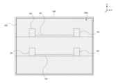
- FIG. 7 is a side view showing an example of a schematic configuration of the microfluidic device 110 in the second embodiment.
- FIG. 7 is a diagram of the microfluidic device 110 of FIG. 6 viewed from the ⁇ X direction, and shows a side surface 100c of the microfluidic device 110.
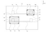
- a transmission window 121 and a transmission window 123 are formed on the side surface 100c of the microfluidic device 100 in the second embodiment.
- the transmission window 121 is provided at the lower left of the side surface 100c, and the transmission window 123 is provided at the upper right of the side surface 100c.
- the transmission window 121 and the transmission window 123 are provided corresponding to the position of the region to be observed in the microfluidic device 110.
- the transmission window 121 and the transmission window 123 are made of a material that transmits illumination light from the outside for observation of the microfluidic device 110, and are made of glass, for example.
- the transmission window 121 and the transmission window 123 in the second embodiment have a flat shape with a constant thickness in the X direction.
- a positioning marker 122 and a positioning marker 124 are formed near the transparent window 121 and the transparent window 123 (for example, near the four corners).
- the vicinity of the transmission window refers to the outside or inside of the transmission window. It is not limited to the vicinity of the four corners, but may be two corners on the diagonal line.
- the positioning marker 122 and the positioning marker 124 are used to search and specify the positions of the transparent window 121 and the transparent window 123.
- the positioning marker 122 and the positioning marker 124 may be formed of a material (metal deposited film, dielectric multilayer film) that has a reflective property for IR (infrared) light emitted from an IR illumination light source 250, which will be described later. Alternatively, it may be made of a material that scatters IR light, or it may be processed with frosted glass that scatters IR light.
- the positioning marker 122 and the positioning marker 124 are different in shape, color, or material.
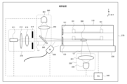
- FIG. 8 shows an example of a schematic configuration of the observation device 270 of the microfluidic device 110 in the second embodiment.
- the observation device 270 includes a sheet illumination optical system 210, an observation optical system 220, a stage 230, a PC 240, an IR illumination light source 250, and a marker observation optical system 260.
- the microfluidic device 110 in the second embodiment further includes an IR illumination light source 250 and a marker observation optical system 260, compared to the microfluidic device 100 in the first embodiment.
- the IR illumination light source 250 and the marker observation optical system 260 are used to confirm the illumination mode of the sheet light L1 from the sheet illumination optical system 210.
- the IR illumination light source 250 illuminates IR light toward at least one of the transmission window 121 and the transmission window 123 in which the positioning marker 122 and the positioning marker 124 are provided.
- IR illumination source 250 includes, for example, at least one infrared light emitting diode (LED).
- LED infrared light emitting diode
- IR illumination source 250 may include multiple LEDs. The IR light is reflected or partially absorbed by at least one of the positioning marker 122 of the transmission window 121 and the positioning marker 124 of the transmission window 123 illuminated with the IR light, and enters the marker observation optical system 260.
- the marker observation optical system 260 includes an IR detector 261, a lens 262, and a dichroic mirror 263.
- the dichroic mirror 263 has a characteristic of transmitting the sheet light L1 and reflecting the IR light.
- the range that can be detected by the marker observation optical system 260 at once is the range that includes the largest transmission window 121 and its positioning marker 122.
- the IR detector 261 is a detector that detects IR light, and is, for example, an image sensor such as an IR-CCD (Charge Coupled Device) image sensor or an IR-CMOS (Complementary Metal Oxide Semiconductor) image sensor.
- the IR light incident on the marker observation optical system 260 is reflected by the dichroic mirror 263, focused by the lens 262, and incident on the IR detector 261.
- Each of the positioning marker 122 and the positioning marker 124 is composed of a plurality of members, but since the plurality of members can be illuminated and observed at once, the respective positions of the transmission window 121 and the transmission window 123 can be adjusted. can be quickly identified.
- the position of the transmission window 121 can be specified. Therefore, for example, if the sheet light L1 travels on the optical axis of the sheet illumination optical system 210 and is incident on the ⁇ Z direction side with respect to the position of the transmission window 121, the desired observation area 300 cannot be illuminated. To do this, the sheet light L1 is transmitted through the transmission window 121 by moving the stage 230 in the -Z direction or by moving the height position of the end face of the optical fiber 211 of the sheet illumination optical system 210 in the +Z direction. The desired observation area 300 can be illuminated using the same method.
- FIG. 9 is a flowchart showing the operation of the observation device 270 of the microfluidic device 110 in the second embodiment.
- the operations of steps S01 to S12 of the observation device 270 in the second embodiment are the same as the operations of steps S01 to S12 of the observation device 200 in the first embodiment.
- the observation device 270 in the second embodiment further includes operations in steps S13 and S14.
- the marker observation optical system 260 detects a positioning marker (for example, positioning marker 122) on a transmission window (for example, transmission window 121). By detecting the positioning marker 122, the position of the transmission window 121 can be specified.
- optimal illumination conditions are set based on information regarding the structure 101 linked to the identified transmission window 121 and information regarding the observation area 300.
- the illumination conditions include, for example, the intensity of the sheet light, the width in the longitudinal direction of the sheet light, the illumination position, the illumination angle, the illumination wavelength, the size of a variable aperture corresponding to the longitudinal width of the sheet light, and the like.
- At least one of the transmission windows 121 and 123 may have an optical function of condensing the sheet light L1 or controlling the traveling direction of the sheet light L1.
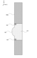
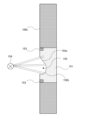
- FIG. 10 shows a transmission window 131 in a first modification.
- FIG. 10 shows a cross-sectional view of the side surface 100c.
- a convex portion 132 having a convex lens function is integrally formed in the transmission window 131 in the first modification, so that the transmission window 131 has a convex lens function as an example of an optical function. Since the transmission window 131 has a convex lens function, it is possible to collimate light from an optical fiber or the like, for example.
- Positioning markers 133 are formed at the four corners of the transmission window 131.
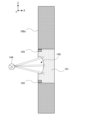
- FIG. 11 shows a transmission window 141 in a second modification.
- FIG. 11 only the side surface 100c of the microfluidic device 110 is illustrated, and other components are omitted.
- FIG. 11 shows a cross-sectional view of the side surface 100c.
- a concave portion 142 having a concave lens function is integrally formed in the transmission window 141 in the second modification, and thus the transmission window 141 has a concave lens function as an example of an optical function.
- An optical scanner 144 that scans the sheet light L1 incident on the transmission window 141 is arranged on the ⁇ X direction side of the transmission window 141, and can scan the sheet light L1 and deflect the sheet light L1 in multiple directions. can.
- the transmission window 141 has a concave lens function, for example, when the sheet light L1 is scanned by the optical scanner 144, the light beam is not refracted at the interface, so that the incident angle of the sheet light L1 can be changed as scanned, and This has the effect of keeping the thickness of the sheet light L1 constant. Further, when it is desired to illuminate with a wide range of illumination light, the light beam of the sheet light L1 can be expanded. Positioning markers 143 are formed at the four corners of the transmission window 141.
- FIG. 12 shows a transmission window 151 in a third modification.
- the transmission window 151 in the third modification is integrally formed with a concave portion 152 consisting of an inclined plane 152a and a curved surface 152b that are inclined with respect to the side surface.
- the inclined plane 152a has a function of allowing illumination light from a specific direction to enter without being refracted.
- the curved surface 152b has a concave lens function as an example of an optical function.
- An optical scanner 154 that scans the sheet light L1 incident on the transmission window 151 is arranged on the ⁇ X direction side of the transmission window 151, and can change the incident angle by scanning the sheet light L1. Since the curved surface 152b of the transmission window 151 has a concave lens function, it can have the same function as the transmission window 141 in the second modification. Further, a plurality of observation areas 300 can be collectively illuminated from the transmission window 151 at a desired angle. Positioning markers 153 are formed at the four corners of the transmission window 151.
- FIG. 13 shows a transmission window 161 in a fourth modification.
- FIG. 13 shows a cross-sectional view of the side surface 100c.
- a plurality of masks 162 are formed in the transmission window 161 in the fourth modification to block part of the sheet light L1 (in a direction that is not desired to be irradiated).
- a plurality of observation regions 300 can be collectively illuminated.
- Positioning markers 163 are formed at the four corners of the transmission window 161.
- the transmission windows 131 to 161 shown in FIGS. 10 to 13 may be combined arbitrarily.
- the mask 162 may be combined with the transmission window 141 having a concave lens function.
- the mask 162 may be combined with the transmission window 151 having a plurality of inclined planes 152a and curved surfaces 152b.
- microfluidic device 110 in the second embodiment the same effects as the microfluidic device 100 in the first embodiment can be achieved.
- a plurality of transmission windows 121 and transmission windows 123 are formed on the side surface 101c. This makes it easy to observe multiple observation areas 300 at different positions.
- the entire side surface 101c is not a transmission surface, but a plurality of transmission windows 121 and transmission windows 123 are formed in a part of the side surface 101c.
- the other parts of the side surface 101c can be made of any material, and material costs can be reduced.
- the four corners of the transmission window 121 and the transmission window 123 are provided with positioning markers 122 and positioning markers for specifying the positions of the transmission window 121 and the transmission window 123.
- 124 is formed, and the observation device 270 further includes an IR illumination light source 250 and a marker observation optical system 260 for detecting the positioning marker 122 and the positioning marker 124.
- the transmission windows 131 to 161 of the first modification to the fourth modification have various optical functions.
- the sheet light L1 from the sheet illumination optical system 210 can be optically manipulated.
- the transmitting surface 102 of the first embodiment may be provided with an optical function.
- the same effects as the microfluidic device 110 in the second embodiment can be achieved.
- an optically transparent portion was provided on the side surface 101c of the microfluidic devices 100, 110, and the observation region 300 was irradiated from the side surface 101c.
- a configuration may also be adopted in which a reflection mirror is provided inside the microfluidic devices 100 and 110 so that the direction of the sheet light L1 irradiated from the side surface 101c can be changed.
- the sheet light L1 irradiated from the side surface 101c is light that travels in a direction generally parallel to the XY plane
- the sheet light L1 irradiated from the side surface 101c may be reflected by a reflective mirror and directed toward the Z direction.
- an optically transparent portion was provided on the side surface 101c of the microfluidic device 100, 110, and the inside was observed by irradiating the sheet light L1 from the side surface 101c.
- the sheet light L1 may be further irradiated from the top surface 101a or the bottom surface 101b of the microfluidic device 100, 110, or the sheet light L1 may be irradiated from the side surface 101c and the top surface 101a or the bottom surface 101b may be combined. good.
- the transmittance of illumination light on the side surfaces other than the side surface 101c on which the transmission surface and the transmission window are formed is actively lowered than on the side surface 101c on which the transmission surface and the transmission window are formed.
- the side surface may be rubbed to make it easier to grip with human hands.
- the side surface may be covered with a light-shielding mask so that external light from the side surface does not affect internal cells.
- two transmission windows 121 and 123 were formed on one side surface 100c of the microfluidic device 110.
- the number of transmission windows formed on one side surface may be three or more.
- a plurality of transmission windows may be formed on each of the plurality of side surfaces. In that case, it is desirable to provide the sheet illumination optical system 210 corresponding to the plurality of side surfaces on which the transmission windows are formed.
- a transmission window was formed on the side surface 100c of the microfluidic device 110, and positioning markers were formed at the four corners of the transmission window.
- the positioning marker may be formed inside the microfluidic device 110 instead of being formed near the transmission window.
- the markers may be formed at parts other than the four corners of the transmission window. The number of markers to be formed does not have to be four.
- FIG. 14 is a diagram showing a modification of the lighting method.
- the sheet illumination optical system 210 was provided in the side direction of the microfluidic devices 100, 110, and the sheet light L1 was irradiated from the side of the microfluidic devices 100, 110 to observe the inside.
- an optical fiber 301 that emits light entirely or a light source unit in which a plurality of LEDs (not shown) are arranged in a straight line is installed on the side of the microfluidic device 100, 110.
- the interior may be illuminated by arranging them parallel to each other (in the XY plane direction).
- the optical fiber 301 and the light source unit may be configured to be movable in the Z direction depending on the position of the transmission window and the position of the observation area. By adjusting the Z position, dark field illumination and bright field illumination can be realized.
- a computer-readable medium may include any tangible device capable of storing instructions for execution by a suitable device, such that the computer-readable medium having instructions stored thereon is illustrated in a flowchart or block diagram.
- An article of manufacture will be provided that includes instructions that can be executed to create a means for performing the operations.
- Examples of computer readable media may include electronic storage media, magnetic storage media, optical storage media, electromagnetic storage media, semiconductor storage media, and the like.
- Computer readable media include floppy disks, diskettes, hard disks, random access memory (RAM), read only memory (ROM), erasable programmable read only memory (EPROM or flash memory), Electrically Erasable Programmable Read Only Memory (EEPROM), Static Random Access Memory (SRAM), Compact Disc Read Only Memory (CD-ROM), Digital Versatile Disk (DVD), Blu-ray (RTM) Disc, Memory Stick, Integrated Circuit cards etc. may be included.
- RAM random access memory
- ROM read only memory
- EPROM or flash memory erasable programmable read only memory
- EEPROM Electrically Erasable Programmable Read Only Memory
- SRAM Static Random Access Memory
- CD-ROM Compact Disc Read Only Memory
- DVD Digital Versatile Disk
- RTM Blu-ray
- Memory Stick Integrated Circuit cards etc.
- Computer-readable instructions may include assembler instructions, Instruction Set Architecture (ISA) instructions, machine instructions, machine-dependent instructions, microcode, firmware instructions, state configuration data, or instructions such as Smalltalk®, JAVA®, C++, etc. any source code or object code written in any combination of one or more programming languages, including object-oriented programming languages and traditional procedural programming languages, such as the "C" programming language or similar programming languages; may include.
- ISA Instruction Set Architecture
- Computer-readable instructions may be implemented on a processor or programmable circuit of a general purpose computer, special purpose computer, or other programmable data processing device, either locally or over a wide area network (WAN), such as a local area network (LAN), the Internet, etc. ), computer-readable instructions may be executed to create a means for performing the operations specified in the flowchart or block diagrams.
- processors include computer processors, processing units, microprocessors, digital signal processors, controllers, microcontrollers, and the like.
- FIG. 15 illustrates an example computer 2200 in which aspects of the invention may be implemented, in whole or in part.
- a program installed on computer 2200 may cause computer 2200 to function as an operation or one or more sections of an apparatus according to an embodiment of the present invention, or to perform one or more operations associated with an apparatus according to an embodiment of the present invention.
- Sections and/or computer 2200 may be caused to perform a process or a step of a process according to an embodiment of the invention.
- Such programs may be executed by CPU 2212 to cause computer 2200 to perform certain operations associated with some or all of the blocks in the flowcharts and block diagrams described herein.
- the computer 2200 includes a CPU 2212, a RAM 2214, a graphics controller 2216, and a display device 2218, which are interconnected by a host controller 2210.
- the computer 2200 also includes input/output units such as a communication interface 2222, a hard disk drive 2224, a DVD-ROM drive 2226, and an IC card drive, which are connected to the host controller 2210 via an input/output controller 2220.
- input/output units such as a communication interface 2222, a hard disk drive 2224, a DVD-ROM drive 2226, and an IC card drive, which are connected to the host controller 2210 via an input/output controller 2220.
- the computer also includes legacy input/output units, such as ROM 2230 and keyboard 2242, which are connected to input/output controller 2220 via input/output chip 2240.
- the CPU 2212 operates according to programs stored in the ROM 2230 and RAM 2214, thereby controlling each unit.
- Graphics controller 2216 obtains image data generated by CPU 2212, such as in a frame buffer provided in RAM 2214 or itself, and causes the image data to be displayed on display device 2218.
- the communication interface 2222 communicates with other electronic devices via the network.
- Hard disk drive 2224 stores programs and data used by CPU 2212 within computer 2200.
- DVD-ROM drive 2226 reads programs or data from DVD-ROM 2201 and provides the programs or data to hard disk drive 2224 via RAM 2214.
- the IC card drive reads programs and data from and/or writes programs and data to the IC card.
- ROM 2230 stores therein programs such as a boot program executed by computer 2200 upon activation and/or programs dependent on the computer 2200 hardware.
- Input/output chip 2240 may also connect various input/output units to input/output controller 2220 via parallel ports, serial ports, keyboard ports, mouse ports, etc.
- a program is provided by a computer readable medium such as a DVD-ROM 2201 or an IC card.
- the program is read from a computer readable medium, installed on hard disk drive 2224, RAM 2214, or ROM 2230, which are also examples of computer readable media, and executed by CPU 2212.
- the information processing described in these programs is read by the computer 2200 and provides coordination between the programs and the various types of hardware resources described above.
- An apparatus or method may be configured to implement the manipulation or processing of information according to the use of computer 2200.
- the CPU 2212 executes a communication program loaded into the RAM 2214 and sends communication processing to the communication interface 2222 based on the processing written in the communication program. You can give orders.
- the communication interface 2222 reads transmission data stored in a transmission buffer processing area provided in a recording medium such as a RAM 2214, a hard disk drive 2224, a DVD-ROM 2201, or an IC card under the control of the CPU 2212, and transmits the read transmission data. Data is transmitted to the network, or received data received from the network is written to a reception buffer processing area provided on the recording medium.
- the CPU 2212 causes the RAM 2214 to read all or a necessary part of a file or database stored in an external recording medium such as a hard disk drive 2224, a DVD-ROM drive 2226 (DVD-ROM 2201), an IC card, etc. Various types of processing may be performed on data on RAM 2214. The CPU 2212 then writes back the processed data to the external recording medium.
- an external recording medium such as a hard disk drive 2224, a DVD-ROM drive 2226 (DVD-ROM 2201), an IC card, etc.
- Various types of processing may be performed on data on RAM 2214.
- the CPU 2212 then writes back the processed data to the external recording medium.
- the CPU 2212 performs various types of operations, information processing, conditional determination, conditional branching, unconditional branching, and information retrieval on the data read from the RAM 2214 as described elsewhere in this disclosure and specified by the instruction sequence of the program. Various types of processing may be performed, including /substitutions, etc., and the results are written back to RAM 2214. Further, the CPU 2212 may search for information in a file in a recording medium, a database, or the like.
- the CPU 2212 search the plurality of entries for an entry that matches the condition, read the attribute value of the second attribute stored in the entry, and thereby associate it with the first attribute that satisfies the predetermined condition.
- the attribute value of the second attribute may be acquired.
- the programs or software modules described above may be stored on computer readable media on or near computer 2200.
- a recording medium such as a hard disk or RAM provided in a server system connected to a dedicated communication network or the Internet can be used as a computer-readable medium, thereby providing the program to the computer 2200 via the network. do.
- 100 microfluidic device 100a top surface, 100b bottom surface, 100c side surface, 100d side surface, 100e side surface, 100f side surface, 101 structure, 101a top surface, 102 transmission surface, 110 microfluidic device, 121 transmission window, 122 positioning marker Ka, 123 Transmission Window, 124 Positioning marker, 131 Transmission window, 132 Convex portion, 133 Positioning marker, 141 Transmission window, 142 Concave portion, 143 Positioning marker, 144 Light scanner, 151 Transmission window, 152 Concave portion, 152a Inclined plane, 152b Curved surface, 153 Positioning marker, 154 Optical scanner, 161 Transmission window, 162 Mask, 163 Positioning marker, 200 Observation device, 210 Sheet illumination optical system, 211 Optical fiber, 212 Collector lens, 213 Cylindrical lens, 214 Variable aperture, 220 Observation optical system, 221 Objective lens, 222 Two-dimensional detector, 230 Stage, 250 IR illumination light source, 260 Marker observation optical system, 2
Landscapes
- Health & Medical Sciences (AREA)
- General Health & Medical Sciences (AREA)
- Immunology (AREA)
- Chemical & Material Sciences (AREA)
- Analytical Chemistry (AREA)
- Biochemistry (AREA)
- Physics & Mathematics (AREA)
- General Physics & Mathematics (AREA)
- Life Sciences & Earth Sciences (AREA)
- Pathology (AREA)
- Nuclear Medicine, Radiotherapy & Molecular Imaging (AREA)
- Apparatus Associated With Microorganisms And Enzymes (AREA)
- Investigating, Analyzing Materials By Fluorescence Or Luminescence (AREA)
- Optical Measuring Cells (AREA)
- Microscoopes, Condenser (AREA)
Abstract
上面および底面と、複数の側面とを有するマイクロ流体デバイスであって、複数の側面の内の少なくとも1つの側面が、外部からの照明光を透過する光学的透過部分を有する、マイクロ流体デバイスを提供する。マイクロ流体デバイスの観察装置であって、上面および底面と、複数の側面とを有し、複数の側面の内の少なくとも1つの側面が、外部からの照明光を透過する光学的透過部分を有するマイクロ流体デバイスに対して、光学的透過部分から照明光を照明する照明光学系と、上面および底面の少なくとも一方からの出力光を受光する観察光学系と、を有する、マイクロ流体デバイスの観察装置を提供する。
Description
本発明は、マイクロ流体デバイス、マイクロ流体デバイスの観察装置、マイクロ流体デバイスの観察方法に関する。
特許文献1には、1または複数の流路が配設されたマイクロ流体デバイスについて、それら流路の内部に存在する被検物を観察するためのマイクロ流体デバイス観察装置及びマイクロ流体デバイス観察方法が記載されている。
[先行技術文献]
[特許文献]
[特許文献1] 国際公開2020/021604号公報
[一般的開示]
[先行技術文献]
[特許文献]
[特許文献1] 国際公開2020/021604号公報
[一般的開示]
本発明の第1の態様においては、上面および底面と、複数の側面とを有するマイクロ流体デバイスであって、複数の側面の内の少なくとも1つの側面が、外部からの照明光を透過する光学的透過部分を有する、マイクロ流体デバイスを提供する。
上記光学的透過部分は、観察の対象となる観察領域に対応して形成されてよい。
上記光学的透過部分は、上記少なくとも1つの側面に複数形成されてよい。
上記1つの側面は、上記光学的透過部分の位置を探索又は特定するためのマーカを有してよい。
上記光学的透過部分は、光学的機能を有してよい。
上記光学的機能は、凸レンズ機能であってよい。
上記光学的機能は、凹レンズ機能であってよい。
上記光学的機能は、上記照明光を複数方向に分離する機能であってよい。
上記光学的透過部分に形成され、上記照明光の一部を遮るマスクを有してよい。
上記光学的透過部分は、観察の対象となる観察領域に対応して形成されたマークを有してよい。
上記上面および上記底面の少なくとも一方は、上記マイクロ流体デバイス内から出力される出力光を透過する光学的透過部分を有してよい。
本発明の第2の態様においては、マイクロ流体デバイスの観察装置であって、上面および底面と、複数の側面とを有し、複数の側面の内の少なくとも1つの側面が、外部からの照明光を透過する光学的透過部分を有するマイクロ流体デバイスに対して、光学的透過部分から照明光を照明する照明光学系と、上面および底面の少なくとも一方からの出力光を受光する観察光学系と、を有する、マイクロ流体デバイスの観察装置を提供する。
上記照明光の、上記光学的透過部分への入射角度が可変であってよい。
上記1つの側面は、上記光学的透過部分の位置を探索又は特定するためのマーカを有し、てよく、上記マーカを観察するマーカ観察光学系、および、上記マーカに照明光を照射する光源をさらに有してよい。
制御装置をさらに有してよく、上記制御装置は、上記光学的透過部分に対応する観察領域に関する情報に基づいて、上記照明光学系を制御して上記照明光を形成してよい。
本発明の第3の態様においては、マイクロ流体デバイスの観察方法であって、上面および底面と、複数の側面とを有し、複数の側面の内の少なくとも1つの側面が、外部からの照明光を透過する光学的透過部分を有するマイクロ流体デバイスに対して、光学的透過部分から照明光を照明する照明段階と、上面および底面の少なくとも一方からの出力光を受光する観察段階と、を有する、マイクロ流体デバイスの観察方法を提供する。
上記照明光の、上記光学的透過部分への入射角度が可変であってよい。
なお、上記の発明の概要は、本発明の必要な特徴の全てを列挙したものではない。また、これらの特徴群のサブコンビネーションもまた、発明となりうる。
以下、発明の実施の形態を通じて本発明を説明する。以下の実施形態は請求の範囲に係る発明を限定するものではない。実施形態の中で説明されている特徴の組み合わせの全てが発明の解決手段に必須であるとは限らない。
図1は、第1の実施形態におけるマイクロ流体デバイス100の概略構成の一例を示す斜視図である。以下、図には、XYZ座標系が示される。図1に示すように、マイクロ流体デバイス(microfluidic devices)100は、上面100aおよび底面100bと、4つの側面100c~100fを有する。上面100aは、マイクロ流体デバイス100を観察のために載置したときに重力方向と反対方向を向いた面であり、底面100bは、マイクロ流体デバイス100を観察のために載置したときに重力方向を向いた面である。4つの側面100c~100fは、上面100aおよび底面100bと直交する面である。側面100cは、マイクロ流体デバイス100の-X方向側を向いた側面であり、側面100dは、マイクロ流体デバイス100の+Y方向側を向いた側面であり、側面100eは、マイクロ流体デバイス100の+X方向側を向いた側面であり、側面100fは、マイクロ流体デバイス100の-Y方向側を向いた側面である。
マイクロ流体デバイス100は複数の層を有しており、マイクロ流体デバイス100の各層には、マイクロ流路、細胞などを注入できる注入口などの構造物101が複数配置されている。本実施形態では、マイクロ流体デバイス100は略直方体形状を有するが、他の立体形状を有するマイクロ流体デバイスに対しても本発明は適用可能である。マイクロ流体デバイス100は、複数の側面の内の少なくとも1つの側面が、外部からの照明光を透過する光学的透過部分である透過面102を有する。照明光は、例えば、蛍光観察であれば可視域又は赤外域の励起光であり、透過や反射での観察であれば、可視域の照明光である。マイクロ流体デバイス100の上面101aまたは底面100bは、観察光を透過する光学的透過部分を有する。観察光は、例えば、蛍光観察であれば可視域の蛍光であり、透過や反射での観察であれば、可視域の観察光である。
マイクロ流体デバイス100とは、小型基板上にDNA、タンパク質、細胞、細胞塊(スフェロイド、オルガノイド等)、組織などの生物学的微細物質に該当する試料を配置して、遺伝子欠陥、タンパク質分布、反応様相などを分析するチップをいう。本実施形態におけるマイクロ流体デバイス100は、臓器チップ(organ on a chip)、生体機能チップ(organ on a chip)、MPS(micro physiological systems)、バイオチップ(bio chip)、マイクロ流体チップ(microfluidic chip)、マイクロチップ(micro chip)、細胞培養チップ、またはマイクロ流路チップ等とも称される。
マイクロ流体デバイス100は、一例として、細胞や組織の培養及び分析に用いられる。さらに、化学物質(薬剤)を添加して培養細胞との反応評価又は分析等に使用される。マイクロ流体デバイス100には、臓器細胞が培養されて生体機能を発現しているものと、まだ臓器細胞が培養されていない「空の」デバイス本体との両方が含まれてよい。
マイクロ流体デバイス100は、例えばステレオリソグラフィー3次元プリンティング技術と、溶液キャストモールディングプロセスとを用いることにより製造することができる。マイクロ流体デバイス100は、上記技術以外にも、例えばMEMS(Micro Electro Mechanical Systems)のような他の微細加工技術により製造することができる。
マイクロ流体デバイス100の各層は、一例として、基板により構成されている。基板は、例えば、ガラスにより構成されていてもよい。基板は、例えば、ポリメチルメタクリレート(PMMA)、ポリカーボネート(PC)、シクロオレフィンコポリマー(COC)、シクロオレフィンポリマー(COP)、ポリスチレン(PS)、シリコーン等の樹脂材料で構成されていてもよい。マイクロ流体デバイス100は、マイクロ流体デバイス100全体を覆うカバーを有していてもよい。
図2は、第1の実施形態におけるマイクロ流体デバイス100の概略構成の一例を示す側面図である。図2は、図1のマイクロ流体デバイス100を-X方向から見たときの図であり、マイクロ流体デバイス100の側面100cを示す。第1の実施形態におけるマイクロ流体デバイス100は、側面100c全体が外部からの照明光を透過する透過面102となっている。外部からの照明光とは、顕微鏡等の観察装置によりマイクロ流体デバイス100を観察する際に、マイクロ流体デバイス100を照明するためにマイクロ流体デバイス100を照明する光である。したがって、透過面102は外部からの照明光を透過する。透過面102は、外部からの照明光を透過する材料で構成され、例えば、ガラスで構成される。透過面102である側面100cは、観察の対象となる観察領域に対応して形成されたマークを有していてもよい。例えば、図2には不図示であるが、後述する図3のような観察領域300が存在する場合、側面100cは、観察領域300の周囲(近傍)に対応する部分(位置)に複数のマークが形成されていてもよい。これにより、観察領域の位置の探索、特定が容易になる。
図3は、第1の実施形態におけるマイクロ流体デバイス100の観察装置200の概略構成の一例を示す。本実施形態における観察装置200は、一例として倒立顕微鏡である。しかしながら、正立顕微鏡も適用可能である。観察装置200は、励起光であるシート光L1をマイクロ流体デバイス100に向けて照明し、観察装置200の蛍光色素から励起された蛍光を撮像することで観察装置200の画像を取得する。シート光L1とはシート形状の照明領域を有する照明光のことである。
図3に示すように、観察装置200はシート照明光学系210と、観察光学系220と、ステージ230と、PC(制御装置)240とを有する。観察装置200のステージ230上にマイクロ流体デバイス100が配置されており、ステージ230が上下方向および左右方向(XYZ方向)に移動することによってマイクロ流体デバイス100を上下方向および左右方向(XYZ方向)に移動可能である。シート照明光学系210、観察光学系220、ステージ230はPC240と接続されており、自動で制御可能である。
シート照明光学系210は、不図示のレーザ光源から出射されたレーザ光を伝搬する光ファイバ211と、コレクタレンズ212と、シリンドリカルレンズ213と、可変絞り214とを有する。シート照明光学系210は、マイクロ流体デバイス100内部の細胞等を照明する照明光学系である。シート照明光学系210は、マイクロ流体デバイス100の側面の-X方向側に配置され、マイクロ流体デバイス100に向けてシート光L1を照明する。シート照明光学系210の構成要素である光ファイバ211の出射端面は点光源を構成し、レーザ光が照射される。レーザ光は、シリンドリカルレンズ213によりシート状の形状を有するシート光L1に成形され、可変絞り214によりシート光が限定されてマイクロ流体デバイス100の観察領域300に向けて照明される。シート光L1は、シート照明光学系210の光軸に直交する方向に長手方向を有する。観察領域300は、ユーザが顕微鏡で観察したいマイクロ流体デバイス100の領域である。
シート光L1は、マイクロ流体デバイス100の側面100cからマイクロ流体デバイス100内部に入射して、マイクロ流体デバイス100内部の細胞等を照明する。図3において、シート光L1はマイクロ流体デバイス100に向けてX軸に平行に照明される。図3に示すように、光ファイバ211の出射端は、シート照明光学系210の光軸から高さ方向(±Z方向)に移動(シフト)可能に構成される。これにより、シート光L1の照明領域を高さ方向(±Z方向)に移動可能に構成することができる。シート光L1の強度および長手方向の幅は、マイクロ流体デバイス100内部の構造物101での乱反射によるゴーストを最小化するように自動で微調整されることが望ましい。
観察光学系220は、対物レンズ221と、不図示の第2対物レンズ(結像レンズ)と、2次元検出器222とを有する。対物レンズ221は、低倍/中高倍電動切り替え可能な構成を有していてもよい。シート照明光学系210から出射したシート光L1は、マイクロ流体デバイス100の観察領域300の細胞に照明される。観察領域300は、細胞に限らず、細胞塊、組織を配置してもよい。観察領域300の細胞からは、シート光L1により励起されて出力光である蛍光L2が出射する。蛍光L2は、マイクロ流体デバイス100の底面100bから出射する。マイクロ流体デバイス100の底面100bは、蛍光L2を透過する素材で構成される。なお、マイクロ流体デバイス100の上面100a方向から観察してもよく、その場合、観察光学系220がマイクロ流体デバイス100の上面100a方向に配置され、上面100aが蛍光L2を透過する素材で構成される。
マイクロ流体デバイス100の底面100bから出射した蛍光L2は、対物レンズ221により集光されて2次元検出器222で検出される。2次元検出器222は、一例としてCCD(Charge Coupled Device)イメージセンサ、sCMOS(scientific Complementary Metal Oxide Semiconductor)イメージセンサ等のイメージセンサである。観察光学系220は、コンデンサレンズや、ダイクロイックミラーなどの他の光学部材をさらに有していてもよい。
PC(制御装置)240は、CPUとメモリ(記憶部)を含み、CPUがメモリに格納されている制御プログラムを読み出し実行することにより、観察装置200の動作を制御する。図3に一点鎖線で示すように、PC240は、顕微鏡のステージ230などと接続されており、顕微鏡全体の動作を制御可能である。PC240は、ユーザからの各種の指示や設定等を受信してPC240の制御部に送信する入力部と、PC240の制御部からの指令を受信してユーザに対してGUI(Graphical User Interface)画面や各種のダイアログ等を表示する表示部とを有している。
図4は、第1の実施形態におけるマイクロ流体デバイス100のシート光L1の角度調整の説明図である。図4は、観察装置200の部分拡大図であり、観察装置200の一部の構成要素のみ図示している。図3において、シート照明光学系210からマイクロ流体デバイス100に入射するシート光L1はX軸に平行であった。しかしながら、図4に示すように、光ファイバ211の出射端面とシート照明光学系210の光軸とのなす角(向き)(チルト)を調整することにより、シート光L1の角度を調整することが可能である。図4に示す例では、光ファイバ211の出射端が斜め上方向を向いており、コレクタレンズ212、シリンドリカルレンズ213を介することにより、シート光L1が斜め下方向の角度をもって観察領域300に照明されている。図4に示すように、シート光L1の角度を調整することにより、例えば、観察領域300を適切な角度から照明することができる。また、観察領域300とシート照明光学系210との間に構造物101等の障害物がある場合に、当該障害物を避けて観察領域300を照明することができる。光ファイバ211の出射端の向き(チルト)の調整と、光ファイバ211の出射端の高さ位置(シフト)(Z方向の位置)の調整は、組み合わせて行うことができる。
図5は、第1の実施形態におけるマイクロ流体デバイス100の観察装置200の動作を示すフローチャートである。ステップS01において、ユーザがマイクロ流体デバイス100を顕微鏡のステージ230に設置する。続いて、ステップS02において、ユーザがGUIにおいてマイクロ流体デバイス100の種別を選択する。
続いて、ステップS03において、ユーザが選択したマイクロ流体デバイス100の種別に基づいて、PC240が、当該種別のマイクロ流体デバイス100の情報を有しているか否かを判別する。マイクロ流体デバイス100の情報とは、例えば、マイクロ流体デバイス100の形状、構造、大きさ、製造業者、培養細胞の情報、型番の内の少なくとも1つの情報を提供する。PC240がマイクロ流体デバイス100の情報を有している場合(ステップS03:YES)、ステップS05に進み、マイクロ流体デバイス100の情報を読出して、ユーザがGUIにて表示されている複数のアッセイから当該マイクロ流体デバイス100に適合するアッセイを選択する。PC240がマイクロ流体デバイス100の情報を有していない場合(ステップS03:NO)、ステップS04に進み、当該マイクロ流体デバイス100が非対応マイクロ流体デバイスである旨のエラーメッセージをGUIに表示する。アッセイとは、画像を取得し、その取得細胞画像に対して、所定の解析、評価処理を行うことで所定の結果を得る画像取得解析ルーチンであり、例えば、細胞数のカウント、細胞密度分布の算出、細胞の生死判定等がある。
続いて、ステップS06において、ユーザがGUIのGOボタンを押下すると、ステップS07に進み、観察装置200がステージ230を動かして、対物レンズ221の視野を最初の観察領域300へ移動する。観察領域300の位置は、ユーザが、GUIに表示されたマイクロ流体デバイス100全体の3次元画像に対して指定可能であり、指定された位置に基づいて、ステップS07の処理は、観察装置200によって自動的に行われる。ステップS07の処理はユーザによって手動で行われてもよい。
続いて、ステップS08において、観察領域300の画像取得を行うために観察条件(照明条件、対物レンズ221の倍率、対物レンズ221と観察領域300との相対位置等を含む)を切り換え、観察領域300の画像を取得する。画像取得の際、ユーザが、GUIに表示されたマイクロ流体デバイス100全体の3次元画像を参照して構造物101を考慮しつつ、最初の観察領域300に対応する透過窓に対して、最適な照明条件を設定し、シート光を照射する。なお、観察領域300に関する情報と、構造物101に関する情報と、透過窓に関する情報とを紐づけて、PC240に記憶させておくことにより、ユーザが、観察領域300を指定するだけで、最初の観察領域300に対応する透過窓に対して、最適な照明条件のシート光が照射されるようにしてもよい。照明条件には、例えば、シート光の強度、シート光の長手方向の幅、照明位置、照明角度、照明波長、シート光の長手方向の幅に対応する可変絞りの大きさなどが含まれる。ステップS09において、取得した観察領域300の画像の画質が良好であるかを確認して、良好であれば(ステップS09:YES)次のステップS10に進む。画質が良好でない場合(ステップS09:NO)には、ステップS08に戻って観察条件を再設定する。
続いて、ステップS10において、次の観察領域があるか否かを判断する。次の観察領域がある場合(ステップS10:YES)には、ステップS07に戻り、ステップS07からS09までの処理を繰り返す。次の観察領域がない場合(ステップS10:NO)には、次のステップS11およびS12に進む。
ステップS11において、アッセイ画像処理(画像分析)を行い、ステップS12において、処理結果(分析結果)を保存する。
上記第1の実施形態におけるマイクロ流体デバイス100によれば、マイクロ流体デバイス100の側面100cが、外部からの照明光を透過する光学的透過部分である透過面102を有する。これにより、マイクロ流体デバイス100を観察するためのシート光L1が、マイクロ流体デバイス100の側面100cからマイクロ流体デバイス100内部に入射可能である。したがって、例えば、マイクロ流体デバイス100の上面101aにマイクロ流路等の構造物101が設置されており、上部から所望の観察領域300を透過観察することが難しい場合においても、側面100cからシート光L1を入射させて観察を行うことができる。
同様に、マイクロ流体デバイス100の内部の構造物101が高さ方向に重なっており、上部から所望の観察領域300をピンポイントで透過観察することが難しい場合や、マイクロ流体デバイス100が多数の層により構成され、高さ方向に分厚いため、上部から所望の観察領域300を透過観察することが難しい場合あっても、側面100cからシート光L1を入射させて観察を行うことができる。
上記第1の実施形態におけるマイクロ流体デバイス100によれば、マイクロ流体デバイス100を観察するためのシート光L1の透過窓に対する入射角度を調整可能である。これにより、マイクロ流体デバイス100内のマイクロ流路等の構造物101をさけて観察領域300をコントラスト良く観察することができる。
上記第1の実施形態におけるマイクロ流体デバイス100の観察装置200によれば、上記第1の実施形態におけるマイクロ流体デバイス100と同様の効果を奏することができる。
図6は、第2の実施形態におけるマイクロ流体デバイス110の概略構成の一例を示す斜視図である。以下、第2の実施形態のマイクロ流体デバイス110の説明に際して、第1の実施形態のマイクロ流体デバイス100と同一の構成については同一の符号を付して説明を省略する。図6に示すように、第2の実施形態におけるマイクロ流体デバイス110には、側面100cに外部からの照明光を透過する光学的透過部分である透過窓121および透過窓123が形成されている。
図7は、第2の実施形態におけるマイクロ流体デバイス110の概略構成の一例を示す側面図である。図7は、図6のマイクロ流体デバイス110を-X方向から見たときの図であり、マイクロ流体デバイス110の側面100cを示す。第2の実施形態におけるマイクロ流体デバイス100の側面100cには、透過窓121および透過窓123が形成される。透過窓121は側面100cの左下部に設けられ、透過窓123は側面100cの右上部に設けられている。透過窓121および透過窓123は、マイクロ流体デバイス110の観察対象となる領域の位置に対応して設けられる。透過窓121および透過窓123は、マイクロ流体デバイス110の観察するための外部からの照明光を透過する材料で構成され、例えば、ガラスで構成される。第2の実施形態における透過窓121および透過窓123は、X方向の厚みが一定な平坦な形状である。
透過窓121および透過窓123の大きさは、側面100c全体の面積に対して十分小さいため、透過窓121または透過窓123の位置を探索するには時間がかかり、また検出の正確性を担保するのも難しい。そのため、透過窓121および透過窓123の近傍(例えば4隅近傍)には、位置だしマーカ122および位置だしマーカ124が形成される。透過窓の近傍とは、透過窓の外側又は内側をいう。4隅近傍に限らず、対角線上の2隅でもよい。位置だしマーカ122および位置だしマーカ124は、透過窓121および透過窓123の位置を探索、特定するために用いられる。位置だしマーカ122および位置だしマーカ124は、後述するIR照明光源250から照射されるIR(infrared:赤外)光の反射特性を有する材料(金属蒸着膜、誘電体多層膜)で形成してもよいし、またはIR光を散乱する特性の材料で形成してもよいし、IR光を散乱させるすりガラス加工を施してもよい。位置だしマーカ122と位置だしマーカ124とは、形状、色、または材料が異なる。
図8は、第2の実施形態におけるマイクロ流体デバイス110の観察装置270の概略構成の一例を示す。図8に示すように、観察装置270はシート照明光学系210と、観察光学系220と、ステージ230と、PC240と、IR照明光源250と、マーカ観察光学系260とを有する。第2の実施形態におけるマイクロ流体デバイス110は、第1の実施形態におけるマイクロ流体デバイス100と比較して、IR照明光源250と、マーカ観察光学系260とをさらに有する。IR照明光源250と、マーカ観察光学系260とは、シート照明光学系210からのシート光L1の照明態様を確認するために用いられる。
IR照明光源250は、位置だしマーカ122および位置だしマーカ124が設けられた透過窓121、および透過窓123の少なくとも1つに向けてIR光を照明する。IR照明光源250は、例えば、少なくとも1つの赤外線発光ダイオード(LED)を備える。IR照明光源250は、複数のLEDを有していてもよい。IR光が照明された、透過窓121の位置だしマーカ122、および透過窓123の位置だしマーカ124の少なくとも一つで、IR光が反射または一部吸収され、マーカ観察光学系260に入射する。
マーカ観察光学系260は、IR検出器261と、レンズ262と、ダイクロイックミラー263とを有する。ダイクロイックミラー263は、シート光L1を透過し、IR光を反射する特性を有する。マーカ観察光学系260が一括で検出できる範囲は、最も大きい透過窓121とその位置だしマーカ122とを包含する範囲である。IR検出器261は、IR光を検出する検出器であり、一例としてIR-CCD(Charge Coupled Device)イメージセンサ、IR-CMOS(Complementary Metal Oxide Semiconductor)イメージセンサ等のイメージセンサである。マーカ観察光学系260に入射したIR光は、ダイクロイックミラー263により反射され、レンズ262により集光されてIR検出器261に入射する。位置だしマーカ122および位置だしマーカ124のそれぞれは、複数の部材から構成されるが、その複数の部材を一括照明し、一括観察することができるので、透過窓121および透過窓123のそれぞれの位置を速やかに特定できる。
IR検出器261で位置だしマーカ122の像を検出することによって、透過窓121の位置を特定することができる。そのため、例えば、シート光L1が、シート照明光学系210の光軸上を進行し、透過窓121の位置よりも-Z方向側に入射しており、所望の観察領域300を照明できていない場合には、ステージ230を-Z方向側に移動するか、シート照明光学系210の光ファイバ211の端面の高さ位置を+Z方向側に移動することにより、シート光L1を、透過窓121を介して所望の観察領域300に照明することができる。
図9は、第2の実施形態におけるマイクロ流体デバイス110の観察装置270の動作を示すフローチャートである。第2の実施形態における観察装置270のステップS01からS12の動作は、第1の実施形態における観察装置200のステップS01からS12の動作と、同じである。第2の実施形態における観察装置270は、ステップS13およびS14の動作をさらに有する。
ステップS13において、マーカ観察光学系260により、透過窓(例えば、透過窓121)の位置だしマーカ(例えば、位置だしマーカ122)を検出する。位置だしマーカ122を検出することにより、透過窓121の位置を特定することができる。次のステップS14において、特定した透過窓121に紐づけられた構造物101に関する情報、観察領域300に関する情報に基づいて最適な照明条件を設定する。照明条件には、例えば、シート光の強度、シート光の長手方向の幅、照明位置、照明角度、照明波長、シート光の長手方向の幅に対応する可変絞りの大きさなどが含まれる。
透過窓121、123の少なくとも一方は、シート光L1を集光したり、シート光L1の進行方向を制御したりする光学的機能を有するようにしてもよい。以下、このような光学的機能を有する変形例を説明する。
図10は、第1の変形例における透過窓131を示す。図10では、マイクロ流体デバイス110の側面100cのみを図示しており、他の構成要素は省略している。図10は、側面100cの断面図を示している。第1の変形例における透過窓131には、凸レンズ機能を有する凸部分132が一体的に形成されており、これにより、透過窓131は光学的機能の一例としての凸レンズ機能を有する。透過窓131が凸レンズ機能を有することにより、例えば、光ファイバ等からの光をコリメートすることができる。透過窓131の4隅には、位置だしマーカ133が形成される。
図11は、第2の変形例における透過窓141を示す。図11では、マイクロ流体デバイス110の側面100cのみを図示しており、他の構成要素は省略している。図11は、側面100cの断面図を示している。第2の変形例における透過窓141には、凹レンズ機能を有する凹部分142が一体的に形成されており、これにより、透過窓141は、光学的機能の一例としての凹レンズ機能を有する。透過窓141の-X方向側には、透過窓141に入射するシート光L1を走査する光スキャナ144が配置されており、シート光L1を走査してシート光L1を複数方向に偏向させることができる。透過窓141が凹レンズ機能を有することにより、例えば、シート光L1を光スキャナ144で走査したときに光束が界面で屈折しないので、走査した通りにシート光L1の入射角度を変えることができ、またシート光L1の太さを一定に保てるという効果を奏する。また、幅広の照明光で照明したいときに、シート光L1の光束を広げられるという効果を奏する。透過窓141の4隅には、位置だしマーカ143が形成される。
図12は、第3の変形例における透過窓151を示す。図12では、マイクロ流体デバイス110の側面100cのみを図示しており、他の構成要素は省略している。図12は、側面100cの断面図を示している。第3の変形例における透過窓151には、側面に対して傾斜している傾斜平面152aおよび曲面152bからなる凹部分152が一体的に形成されている。傾斜平面152aは、光学的機能の一例として、特定の方向からの照明光を屈折させずに入射する機能を有する。曲面152bは、光学的機能の一例として、凹レンズ機能を有する。透過窓151の-X方向側には、透過窓151に入射するシート光L1を走査する光スキャナ154が配置されており、シート光L1を走査して入射角度を変化させることができる。透過窓151の曲面152bが凹レンズ機能を有することにより、上記第2の変形例における透過窓141と同様の機能を有することができる。また、透過窓151から複数の観察領域300を所望の角度でまとめて照明できる。透過窓151の4隅には、位置だしマーカ153が形成される。
図13は、第4の変形例における透過窓161を示す。図13では、マイクロ流体デバイス110の側面100cのみを図示しており、他の構成要素は省略している。図13は、側面100cの断面図を示している。第4の変形例における透過窓161には、シート光L1の一部(照射したくない方向)を遮るマスク162が複数形成されており、これにより、透過窓161は光学的機能の一例として光遮蔽機能を有する。透過窓161が光遮蔽機能を有することにより、例えば、シート光L1の光束の大きさを調整することができる。また、マイクロ流体デバイス110に対して一括照明を行い、マスク162で、照射した方向に複数の光束を生成することで、複数の観察領域300をまとめて照明できる。透過窓161の4隅には、位置だしマーカ163が形成される。
図10から13に示す透過窓131~161は、任意に組み合わせてもよい。例えば、凹レンズ機能を有する透過窓141に、マスク162を組み合わせてもよい。また、複数の傾斜平面152aおよび曲面152bを有する透過窓151に、マスク162を組み合わせてもよい。
上記第2の実施形態におけるマイクロ流体デバイス110によれば、上記第1の実施形態におけるマイクロ流体デバイス100と同様の効果を奏することができる。
上記第2の実施形態におけるマイクロ流体デバイス110によれば、側面101cに複数の透過窓121および透過窓123が形成される。これにより、異なる位置の複数の観察領域300を観察することが容易となる。
上記第2の実施形態におけるマイクロ流体デバイス110によれば、側面101c全体が透過面ではなく、側面101cの一部に複数の透過窓121および透過窓123が形成される。これにより、側面101cの他の部分は任意の材料で構成することができ、材料費を削減できる。
上記第2の実施形態におけるマイクロ流体デバイス110によれば、透過窓121および透過窓123の4隅には、透過窓121および透過窓123の位置を特定するための位置だしマーカ122および位置だしマーカ124が形成され、観察装置270は、位置だしマーカ122、位置だしマーカ124を検出するための、IR照明光源250と、マーカ観察光学系260をさらに有する。これにより、透過窓121および透過窓123を迅速に検出することができる。
上記第2の実施形態におけるマイクロ流体デバイス110によれば、第1の変形例から第4の変形例の透過窓131~161は様々な光学的機能を有する。これにより、シート照明光学系210からのシート光L1を光学的に操作可能である。なお、第1の実施形態の透過面102に光学的機能を設けてもよい。
上記第2の実施形態におけるマイクロ流体デバイス110の観察装置270によれば、上記第2の実施形態におけるマイクロ流体デバイス110と同様の効果を奏することができる。
上記第1および第2の実施形態において、マイクロ流体デバイス100、110の側面101cに光学的透過部分を設け、側面101cから観察領域300を照射した。しかしながら、マイクロ流体デバイス100、110の内部に反射ミラーを設けて、側面101cから照射されたシート光L1の方向を変更可能な構成としてもよい。例えば、側面101cから照射されたシート光L1は概ねXY平面に平行な方向に進む光であるが、側面101cから照射されたシート光L1を反射ミラーで反射してZ方向に向けてもよい。
上記第1および第2の実施形態において、マイクロ流体デバイス100、110の側面101cに光学的透過部分を設け、側面101cからシート光L1を照射して内部を観察した。しかしながら、マイクロ流体デバイス100、110の上面101aまたは底面101bからさらにシート光L1を照射してもよく、側面101cから照射する態様と上面101aまたは底面101bから照射する態様とを組み合わせて実施してもよい。
上記第1および第2の実施形態において、透過面および透過窓が形成された側面101c以外の側面における照明光の透過率を、透過面及び透過窓が形成された側面101cより積極的に低くしてもよい。例えば、当該側面が、人の手で把持しやすいように擦り加工されていてもよい。また、当該側面からの外光で内部の細胞に影響を与えないように、当該側面を遮光のマスクで覆ってもよい。
上記第2の実施形態において、マイクロ流体デバイス110の1つの側面100cに2つの透過窓121および透過窓123を形成した。しかしながら、1つの側面に形成する透過窓の数は3以上であってもよい。また、複数の側面にそれぞれ複数の透過窓を形成してもよい。その場合、シート照明光学系210を透過窓が形成された複数の側面に対応して設けることが望ましい。
上記第2の実施形態において、マイクロ流体デバイス110の側面100cに透過窓を形成し、透過窓の4隅に位置だしマーカを形成した。しかしながら、位置だしマーカを透過窓の近傍に形成せずに、マイクロ流体デバイス110の内部に形成してもよい。また、マーカは透過窓の4隅以外の部分に形成してもよい。形成するマーカの数は4つでなくてもよい。
図14は、照明方法の変形例を示す図である。上記第1および第2の実施形態において、マイクロ流体デバイス100、110の側面方向にシート照明光学系210を設け、マイクロ流体デバイス100、110の側面からシート光L1を照射して内部を観察した。しかしながら、図14に示すように、シート照明光学系210の代わりに、全体が発光する光ファイバ301、または不図示の複数LEDが直線状に並んだ光源ユニットをマイクロ流体デバイス100、110の側面に沿って平行に(XY平面方向に)配置して内部を照明してもよい。その場合、透過面または透過窓を光ファイバ301が配置された側面に対応して設けることが望ましい。光ファイバ301、光源ユニットは、透過窓の位置、観察領域の位置に応じて、Z方向に移動できるように構成してもよい。Z位置を調整することによって、暗視野照明、明視野照明を実現することができる。
また、本発明の様々な実施形態は、フローチャートおよびブロック図を参照して記載されてよく、ここにおいてブロックは、(1)操作が実行されるプロセスの段階または(2)操作を実行する役割を持つ装置のセクションを表わしてよい。特定の段階およびセクションが、専用回路、コンピュータ可読媒体上に格納されるコンピュータ可読命令と共に供給されるプログラマブル回路、および/またはコンピュータ可読媒体上に格納されるコンピュータ可読命令と共に供給されるプロセッサによって実装されてよい。専用回路は、デジタルおよび/またはアナログハードウェア回路を含んでよく、集積回路(IC)および/またはディスクリート回路を含んでよい。プログラマブル回路は、論理AND、論理OR、論理XOR、論理NAND、論理NOR、および他の論理操作、フリップフロップ、レジスタ、フィールドプログラマブルゲートアレイ(FPGA)、プログラマブルロジックアレイ(PLA)等のようなメモリ要素等を含む、再構成可能なハードウェア回路を含んでよい。
コンピュータ可読媒体は、適切なデバイスによって実行される命令を格納可能な任意の有形なデバイスを含んでよく、その結果、そこに格納される命令を有するコンピュータ可読媒体は、フローチャートまたはブロック図で指定された操作を実行するための手段を作成すべく実行され得る命令を含む、製品を備えることになる。コンピュータ可読媒体の例としては、電子記憶媒体、磁気記憶媒体、光記憶媒体、電磁記憶媒体、半導体記憶媒体等が含まれてよい。コンピュータ可読媒体のより具体的な例としては、フロッピー(登録商標)ディスク、ディスケット、ハードディスク、ランダムアクセスメモリ(RAM)、リードオンリメモリ(ROM)、消去可能プログラマブルリードオンリメモリ(EPROMまたはフラッシュメモリ)、電気的消去可能プログラマブルリードオンリメモリ(EEPROM)、静的ランダムアクセスメモリ(SRAM)、コンパクトディスクリードオンリメモリ(CD-ROM)、デジタル多用途ディスク(DVD)、ブルーレイ(RTM)ディスク、メモリスティック、集積回路カード等が含まれてよい。
コンピュータ可読命令は、アセンブラ命令、命令セットアーキテクチャ(ISA)命令、マシン命令、マシン依存命令、マイクロコード、ファームウェア命令、状態設定データ、またはSmalltalk(登録商標)、JAVA(登録商標)、C++等のようなオブジェクト指向プログラミング言語、および「C」プログラミング言語または同様のプログラミング言語のような従来の手続型プログラミング言語を含む、1または複数のプログラミング言語の任意の組み合わせで記述されたソースコードまたはオブジェクトコードのいずれかを含んでよい。
コンピュータ可読命令は、汎用コンピュータ、特殊目的のコンピュータ、若しくは他のプログラム可能なデータ処理装置のプロセッサまたはプログラマブル回路に対し、ローカルにまたはローカルエリアネットワーク(LAN)、インターネット等のようなワイドエリアネットワーク(WAN)を介して提供され、フローチャートまたはブロック図で指定された操作を実行するための手段を作成すべく、コンピュータ可読命令を実行してよい。プロセッサの例としては、コンピュータプロセッサ、処理ユニット、マイクロプロセッサ、デジタル信号プロセッサ、コントローラ、マイクロコントローラ等を含む。
図15は、本発明の複数の態様が全体的または部分的に具現化されてよいコンピュータ2200の例を示す。コンピュータ2200にインストールされたプログラムは、コンピュータ2200に、本発明の実施形態に係る装置に関連付けられる操作または当該装置の1または複数のセクションとして機能させることができ、または当該操作または当該1または複数のセクションを実行させることができ、および/またはコンピュータ2200に、本発明の実施形態に係るプロセスまたは当該プロセスの段階を実行させることができる。そのようなプログラムは、コンピュータ2200に、本明細書に記載のフローチャートおよびブロック図のブロックのうちのいくつかまたはすべてに関連付けられた特定の操作を実行させるべく、CPU2212によって実行されてよい。
本実施形態によるコンピュータ2200は、CPU2212、RAM2214、グラフィックコントローラ2216、およびディスプレイデバイス2218を含み、それらはホストコントローラ2210によって相互に接続されている。コンピュータ2200はまた、通信インタフェース2222、ハードディスクドライブ2224、DVD-ROMドライブ2226、およびICカードドライブのような入/出力ユニットを含み、それらは入/出力コントローラ2220を介してホストコントローラ2210に接続されている。コンピュータはまた、ROM2230およびキーボード2242のようなレガシの入/出力ユニットを含み、それらは入/出力チップ2240を介して入/出力コントローラ2220に接続されている。
CPU2212は、ROM2230およびRAM2214内に格納されたプログラムに従い動作し、それにより各ユニットを制御する。グラフィックコントローラ2216は、RAM2214内に提供されるフレームバッファ等またはそれ自体の中にCPU2212によって生成されたイメージデータを取得し、イメージデータがディスプレイデバイス2218上に表示されるようにする。
通信インタフェース2222は、ネットワークを介して他の電子デバイスと通信する。ハードディスクドライブ2224は、コンピュータ2200内のCPU2212によって使用されるプログラムおよびデータを格納する。DVD-ROMドライブ2226は、プログラムまたはデータをDVD-ROM2201から読み取り、ハードディスクドライブ2224にRAM2214を介してプログラムまたはデータを提供する。ICカードドライブは、プログラムおよびデータをICカードから読み取り、および/またはプログラムおよびデータをICカードに書き込む。
ROM2230はその中に、アクティブ化時にコンピュータ2200によって実行されるブートプログラム等、および/またはコンピュータ2200のハードウェアに依存するプログラムを格納する。入/出力チップ2240はまた、様々な入/出力ユニットをパラレルポート、シリアルポート、キーボードポート、マウスポート等を介して、入/出力コントローラ2220に接続してよい。
プログラムが、DVD-ROM2201またはICカードのようなコンピュータ可読媒体によって提供される。プログラムは、コンピュータ可読媒体から読み取られ、コンピュータ可読媒体の例でもあるハードディスクドライブ2224、RAM2214、またはROM2230にインストールされ、CPU2212によって実行される。これらのプログラム内に記述される情報処理は、コンピュータ2200に読み取られ、プログラムと、上記様々なタイプのハードウェアリソースとの間の連携をもたらす。装置または方法が、コンピュータ2200の使用に従い情報の操作または処理を実現することによって構成されてよい。
例えば、通信がコンピュータ2200および外部デバイス間で実行される場合、CPU2212は、RAM2214にロードされた通信プログラムを実行し、通信プログラムに記述された処理に基づいて、通信インタフェース2222に対し、通信処理を命令してよい。通信インタフェース2222は、CPU2212の制御下、RAM2214、ハードディスクドライブ2224、DVD-ROM2201、またはICカードのような記録媒体内に提供される送信バッファ処理領域に格納された送信データを読み取り、読み取られた送信データをネットワークに送信し、またはネットワークから受信された受信データを記録媒体上に提供される受信バッファ処理領域等に書き込む。
また、CPU2212は、ハードディスクドライブ2224、DVD-ROMドライブ2226(DVD-ROM2201)、ICカード等のような外部記録媒体に格納されたファイルまたはデータベースの全部または必要な部分がRAM2214に読み取られるようにし、RAM2214上のデータに対し様々なタイプの処理を実行してよい。CPU2212は次に、処理されたデータを外部記録媒体にライトバックする。
様々なタイプのプログラム、データ、テーブル、およびデータベースのような様々なタイプの情報が記録媒体に格納され、情報処理を受けてよい。CPU2212は、RAM2214から読み取られたデータに対し、本開示の随所に記載され、プログラムの命令シーケンスによって指定される様々なタイプの操作、情報処理、条件判断、条件分岐、無条件分岐、情報の検索/置換等を含む、様々なタイプの処理を実行してよく、結果をRAM2214に対しライトバックする。また、CPU2212は、記録媒体内のファイル、データベース等における情報を検索してよい。例えば、各々が第2の属性の属性値に関連付けられた第1の属性の属性値を有する複数のエントリが記録媒体内に格納される場合、CPU2212は、第1の属性の属性値が指定される、条件に一致するエントリを当該複数のエントリの中から検索し、当該エントリ内に格納された第2の属性の属性値を読み取り、それにより予め定められた条件を満たす第1の属性に関連付けられた第2の属性の属性値を取得してよい。
上で説明したプログラムまたはソフトウェアモジュールは、コンピュータ2200上またはコンピュータ2200近傍のコンピュータ可読媒体に格納されてよい。また、専用通信ネットワークまたはインターネットに接続されたサーバーシステム内に提供されるハードディスクまたはRAMのような記録媒体が、コンピュータ可読媒体として使用可能であり、それによりプログラムを、ネットワークを介してコンピュータ2200に提供する。
以上、本発明を実施の形態を用いて説明したが、本発明の技術的範囲は上記実施の形態に記載の範囲には限定されない。上記実施の形態に、多様な変更または改良を加えることが可能であることが当業者に明らかである。その様な変更または改良を加えた形態も本発明の技術的範囲に含まれ得ることが、請求の範囲の記載から明らかである。
請求の範囲、明細書、および図面中において示した装置、システム、プログラム、および方法における動作、手順、ステップ、および段階等の各処理の実行順序は、特段「より前に」、「先立って」等と明示しておらず、また、前の処理の出力を後の処理で用いるのでない限り、任意の順序で実現しうることに留意すべきである。請求の範囲、明細書、および図面中の動作フローに関して、便宜上「まず、」、「次に、」等を用いて説明したとしても、この順で実施することが必須であることを意味するものではない。
100 マイクロ流体デバイス、100a 上面、100b 底面、100c 側面、100d 側面、100e 側面、100f 側面、101 構造物、101a 上面、102 透過面、110 マイクロ流体デバイス、121 透過窓、122 位置だしマーカ、123 透過窓、124 位置だしマーカ、131 透過窓、132 凸部分、133 位置だしマーカ、141 透過窓、142 凹部分、143 位置だしマーカ、144 光スキャナ、151 透過窓、152 凹部分、152a 傾斜平面、152b 曲面、153 位置だしマーカ、154 光スキャナ、161 透過窓、162 マスク、163 位置だしマーカ、200 観察装置、210 シート照明光学系、211 光ファイバ、212 コレクタレンズ、213 シリンドリカルレンズ、214 可変絞り、220 観察光学系、221 対物レンズ、222 2次元検出器、230 ステージ、250 IR照明光源、260 マーカ観察光学系、261 IR検出器、262 レンズ、263 ダイクロイックミラー、270 観察装置、300 観察領域、301 光ファイバ、2200 コンピュータ、2201 DVD-ROM、2210 ホストコントローラ、2212 CPU、2214 RAM、2216 グラフィックコントローラ、2218 ディスプレイデバイス、2220 入/出力コントローラ、2222 通信インタフェース、2224 ハードディスクドライブ、2226 DVD-ROMドライブ、2230 ROM、2240 入/出力チップ、2242 キーボード
Claims (17)
- 上面および底面と、複数の側面とを有するマイクロ流体デバイスであって、
前記複数の側面の内の少なくとも1つの側面が、外部からの照明光を透過する光学的透過部分を有する、
マイクロ流体デバイス。 - 前記光学的透過部分は、観察の対象となる観察領域に対応して形成される、請求項1に記載のマイクロ流体デバイス。
- 前記光学的透過部分は、前記少なくとも1つの側面に複数形成される、請求項1または2に記載のマイクロ流体デバイス。
- 前記1つの側面は、前記光学的透過部分の位置を探索又は特定するためのマーカを有する、請求項1から3のいずれか1項に記載のマイクロ流体デバイス。
- 前記光学的透過部分は、光学的機能を有する、請求項1から4のいずれか1項に記載のマイクロ流体デバイス。
- 前記光学的機能は、凸レンズ機能である、請求項5に記載のマイクロ流体デバイス。
- 前記光学的機能は、凹レンズ機能である、請求項5に記載のマイクロ流体デバイス。
- 前記光学的機能は、前記照明光を複数方向に分離する機能である、請求項5に記載のマイクロ流体デバイス。
- 前記光学的透過部分に形成され、前記照明光の一部を遮るマスクを有する、請求項1から8のいずれか1項に記載のマイクロ流体デバイス。
- 前記光学的透過部分は、観察の対象となる観察領域に対応して形成されたマークを有する、請求項1から9のいずれか1項に記載のマイクロ流体デバイス。
- 前記上面および前記底面の少なくとも一方は、前記マイクロ流体デバイス内から出力される出力光を透過する光学的透過部分を有する、請求項1から10のいずれか1項に記載のマイクロ流体デバイス。
- マイクロ流体デバイスの観察装置であって、
上面および底面と、複数の側面とを有し、前記複数の側面の内の少なくとも1つの側面が、外部からの照明光を透過する光学的透過部分を有するマイクロ流体デバイスに対して、前記光学的透過部分から前記照明光を照明する照明光学系と、
前記上面および前記底面の少なくとも一方からの出力光を受光する観察光学系と、を有する、
マイクロ流体デバイスの観察装置。 - 前記照明光の、前記光学的透過部分への入射角度が可変である、請求項12に記載のマイクロ流体デバイスの観察装置。
- 前記1つの側面は、前記光学的透過部分の位置を探索又は特定するためのマーカを有し、
前記マーカを観察するマーカ観察光学系、および、前記マーカに照明光を照射する光源をさらに有する、請求項12または13に記載のマイクロ流体デバイスの観察装置。 - 制御装置をさらに有し、
前記制御装置は、前記光学的透過部分に対応する観察領域に関する情報に基づいて、前記照明光学系を制御して前記照明光を形成する、請求項12から14のいずれか1項に記載のマイクロ流体デバイスの観察装置。 - マイクロ流体デバイスの観察方法であって、
上面および底面と、複数の側面とを有し、前記複数の側面の内の少なくとも1つの側面が、外部からの照明光を透過する光学的透過部分を有するマイクロ流体デバイスに対して、
前記光学的透過部分から前記照明光を照明する照明段階と、
前記上面および前記底面の少なくとも一方からの出力光を受光する観察段階と、を有する、マイクロ流体デバイスの観察方法。 - 前記照明光の、前記光学的透過部分への入射角度が可変である、請求項16に記載のマイクロ流体デバイスの観察方法。
Applications Claiming Priority (2)
| Application Number | Priority Date | Filing Date | Title |
|---|---|---|---|
| JP2022119218A JP2025128424A (ja) | 2022-07-27 | 2022-07-27 | マイクロ流体デバイス、マイクロ流体デバイスの観察装置、マイクロ流体デバイスの観察方法 |
| JP2022-119218 | 2022-07-27 |
Publications (1)
| Publication Number | Publication Date |
|---|---|
| WO2024024697A1 true WO2024024697A1 (ja) | 2024-02-01 |
Family
ID=89706527
Family Applications (1)
| Application Number | Title | Priority Date | Filing Date |
|---|---|---|---|
| PCT/JP2023/026894 Ceased WO2024024697A1 (ja) | 2022-07-27 | 2023-07-21 | マイクロ流体デバイス、マイクロ流体デバイスの観察装置、マイクロ流体デバイスの観察方法 |
Country Status (2)
| Country | Link |
|---|---|
| JP (1) | JP2025128424A (ja) |
| WO (1) | WO2024024697A1 (ja) |
Cited By (1)
| Publication number | Priority date | Publication date | Assignee | Title |
|---|---|---|---|---|
| CN118150561A (zh) * | 2024-03-29 | 2024-06-07 | 追光生物科技(深圳)有限公司 | 一种便携式的微流控观察和检测系统 |
Citations (3)
| Publication number | Priority date | Publication date | Assignee | Title |
|---|---|---|---|---|
| JP2005188999A (ja) * | 2003-12-24 | 2005-07-14 | Matsushita Electric Ind Co Ltd | 特定成分の濃度測定装置、特定成分の濃度測定方法 |
| JP2018097001A (ja) * | 2018-01-09 | 2018-06-21 | 株式会社東芝 | 光学センサ、分析装置および分析方法 |
| WO2020085104A1 (ja) * | 2018-10-24 | 2020-04-30 | 凸版印刷株式会社 | 免疫測定用カップ及びその製造方法、並びに免疫測定方法 |
-
2022
- 2022-07-27 JP JP2022119218A patent/JP2025128424A/ja active Pending
-
2023
- 2023-07-21 WO PCT/JP2023/026894 patent/WO2024024697A1/ja not_active Ceased
Patent Citations (3)
| Publication number | Priority date | Publication date | Assignee | Title |
|---|---|---|---|---|
| JP2005188999A (ja) * | 2003-12-24 | 2005-07-14 | Matsushita Electric Ind Co Ltd | 特定成分の濃度測定装置、特定成分の濃度測定方法 |
| JP2018097001A (ja) * | 2018-01-09 | 2018-06-21 | 株式会社東芝 | 光学センサ、分析装置および分析方法 |
| WO2020085104A1 (ja) * | 2018-10-24 | 2020-04-30 | 凸版印刷株式会社 | 免疫測定用カップ及びその製造方法、並びに免疫測定方法 |
Cited By (1)
| Publication number | Priority date | Publication date | Assignee | Title |
|---|---|---|---|---|
| CN118150561A (zh) * | 2024-03-29 | 2024-06-07 | 追光生物科技(深圳)有限公司 | 一种便携式的微流控观察和检测系统 |
Also Published As
| Publication number | Publication date |
|---|---|
| JP2025128424A (ja) | 2025-09-03 |
Similar Documents
| Publication | Publication Date | Title |
|---|---|---|
| US12461355B2 (en) | Open-top light-sheet microscopy with a non-orthogonal arrangement of illumination and collection objectives | |
| CN107526156B (zh) | 光片显微镜以及用于运行光片显微镜的方法 | |
| JP6925361B2 (ja) | サンプル場所のための補助画像検出器を有する撮像システム | |
| CN101438147A (zh) | 生物试样摄像方法及生物试样摄像装置 | |
| JP2021113806A (ja) | 生体試料を熱サイクルするための装置、それを含む監視機器、およびそのような装置を使用して生体試料を熱サイクルする方法 | |
| CN100392098C (zh) | 微阵列生物芯片的反射式图像获取装置与分析方法 | |
| CN109643012B (zh) | 观察装置 | |
| JP2012123039A (ja) | 顕微鏡、領域判定方法、及びプログラム | |
| CN116802463A (zh) | 具有共焦成像的用于微孔板的通用多功能检测系统 | |
| JP6796379B2 (ja) | レーザーマイクロダイセクター及びレーザーマイクロダイセクション方法 | |
| Oheim | High‐throughput microscopy must re‐invent the microscope rather than speed up its functions | |
| JP2026002855A (ja) | 支援システム、支援方法、情報処理装置、及びプログラム | |
| US20240111945A1 (en) | Experiment support apparatus, experiment support system, experiment support method, and computer-readable medium | |
| US20090292479A1 (en) | Method for analyzing image from bio-detection analyzer | |
| JP2012039929A (ja) | 受精卵観察の画像処理方法、画像処理プログラム及び画像処理装置、並びに受精卵の製造方法 | |
| JP2025128424A (ja) | マイクロ流体デバイス、マイクロ流体デバイスの観察装置、マイクロ流体デバイスの観察方法 | |
| US20250231389A1 (en) | Holder apparatus and observation apparatus | |
| JP2022509823A (ja) | 細胞培養監視のための小型光学結像システム | |
| US20250264707A1 (en) | Observation apparatus | |
| JP2010066212A (ja) | 測定装置及び観察対象の測定方法 | |
| JP2024016932A (ja) | マイクロ流体デバイス、マイクロ流体デバイスの観察装置、マイクロ流体デバイスの観察方法 | |
| US6597522B2 (en) | Optical system | |
| JP2023019080A (ja) | 観察システム、プログラム、及び観察方法 | |
| JP2024025864A (ja) | マイクロ流体デバイス、マイクロ流体デバイス用観察装置、マイクロ流体デバイスの観察方法 | |
| JP7693187B2 (ja) | 検査装置 |
Legal Events
| Date | Code | Title | Description |
|---|---|---|---|
| 121 | Ep: the epo has been informed by wipo that ep was designated in this application |
Ref document number: 23846427 Country of ref document: EP Kind code of ref document: A1 |
|
| NENP | Non-entry into the national phase |
Ref country code: DE |
|
| 122 | Ep: pct application non-entry in european phase |
Ref document number: 23846427 Country of ref document: EP Kind code of ref document: A1 |
|
| NENP | Non-entry into the national phase |
Ref country code: JP |