WO2024024491A1 - 表示装置及び電子機器 - Google Patents
表示装置及び電子機器 Download PDFInfo
- Publication number
- WO2024024491A1 WO2024024491A1 PCT/JP2023/025539 JP2023025539W WO2024024491A1 WO 2024024491 A1 WO2024024491 A1 WO 2024024491A1 JP 2023025539 W JP2023025539 W JP 2023025539W WO 2024024491 A1 WO2024024491 A1 WO 2024024491A1
- Authority
- WO
- WIPO (PCT)
- Prior art keywords
- display device
- light emitting
- layer
- lens
- light
- Prior art date
- Legal status (The legal status is an assumption and is not a legal conclusion. Google has not performed a legal analysis and makes no representation as to the accuracy of the status listed.)
- Ceased
Links
Images
















Classifications
-
- G—PHYSICS
- G02—OPTICS
- G02B—OPTICAL ELEMENTS, SYSTEMS OR APPARATUS
- G02B5/00—Optical elements other than lenses
- G02B5/20—Filters
-
- G—PHYSICS
- G09—EDUCATION; CRYPTOGRAPHY; DISPLAY; ADVERTISING; SEALS
- G09F—DISPLAYING; ADVERTISING; SIGNS; LABELS OR NAME-PLATES; SEALS
- G09F9/00—Indicating arrangements for variable information in which the information is built-up on a support by selection or combination of individual elements
- G09F9/30—Indicating arrangements for variable information in which the information is built-up on a support by selection or combination of individual elements in which the desired character or characters are formed by combining individual elements
-
- H—ELECTRICITY
- H10—SEMICONDUCTOR DEVICES; ELECTRIC SOLID-STATE DEVICES NOT OTHERWISE PROVIDED FOR
- H10K—ORGANIC ELECTRIC SOLID-STATE DEVICES
- H10K50/00—Organic light-emitting devices
- H10K50/80—Constructional details
- H10K50/84—Passivation; Containers; Encapsulations
- H10K50/844—Encapsulations
-
- H—ELECTRICITY
- H10—SEMICONDUCTOR DEVICES; ELECTRIC SOLID-STATE DEVICES NOT OTHERWISE PROVIDED FOR
- H10K—ORGANIC ELECTRIC SOLID-STATE DEVICES
- H10K50/00—Organic light-emitting devices
- H10K50/80—Constructional details
- H10K50/85—Arrangements for extracting light from the devices
- H10K50/858—Arrangements for extracting light from the devices comprising refractive means, e.g. lenses
-
- H—ELECTRICITY
- H10—SEMICONDUCTOR DEVICES; ELECTRIC SOLID-STATE DEVICES NOT OTHERWISE PROVIDED FOR
- H10K—ORGANIC ELECTRIC SOLID-STATE DEVICES
- H10K59/00—Integrated devices, or assemblies of multiple devices, comprising at least one organic light-emitting element covered by group H10K50/00
- H10K59/10—OLED displays
-
- H—ELECTRICITY
- H10—SEMICONDUCTOR DEVICES; ELECTRIC SOLID-STATE DEVICES NOT OTHERWISE PROVIDED FOR
- H10K—ORGANIC ELECTRIC SOLID-STATE DEVICES
- H10K59/00—Integrated devices, or assemblies of multiple devices, comprising at least one organic light-emitting element covered by group H10K50/00
- H10K59/30—Devices specially adapted for multicolour light emission
- H10K59/38—Devices specially adapted for multicolour light emission comprising colour filters or colour changing media [CCM]
Definitions
- the present disclosure relates to display devices and electronic devices.
- Display devices using light emitting elements such as organic EL elements are installed in devices such as virtual reality (VR) and electronic viewfinders (EVF).
- VR virtual reality
- EVF electronic viewfinders
- viewing angle correction is performed in order to meet demands for smaller size and lighter weight.
- Patent Documents 1 and 2 disclose a technique for shifting the center position of a color filter or a lens according to the position of a subpixel in a display area.
- Patent Documents 1 and 2 have room for improvement in terms of suppressing brightness loss in subpixels near the outer periphery of the display area and improving viewing angle characteristics near the outer periphery of the display area. .
- the present disclosure has been made in view of the above-mentioned points, and is capable of suppressing brightness loss in subpixels near the outer periphery of the display area, and further improving viewing angle characteristics near the outer periphery of the display area.
- One of its purposes is to provide display devices and electronic equipment.
- the present disclosure includes, for example, (1) a display area including a plurality of subpixels two-dimensionally arranged in the display area; Each of the sub-pixels has a light emitting part, and at least a light emitting element is formed in the light emitting part, At least some of the plurality of subpixels include a structure that controls the traveling direction of at least some of the light generated from the light emitting element, the structures provided in different subpixels are separated from each other; It is a display device.
- the present disclosure may be (2) an electronic device including the display device described in (1) above.
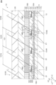
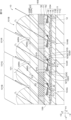
- FIG. 1 is a sectional view for explaining an example of a display device according to a first embodiment.
- FIG. 2A is a plan view for explaining one embodiment of the display device.
- FIG. 2B is a diagram showing the main optical axis of the sub-pixel in an enlarged portion of the region XS1 surrounded by the broken line in FIG. 2A.
- FIG. 2C is a diagram showing the main optical axis of the sub-pixel in an enlarged portion of the region XS2 surrounded by the broken line in FIG. 2A.
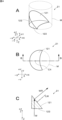
- FIG. 3A is a perspective view for explaining one embodiment of the structure.
- FIG. 3B is a plan view for explaining one embodiment of the structure.
- FIG. 3C is a cross-sectional view for explaining one embodiment of the structure.
- FIG. 3A is a perspective view for explaining one embodiment of the structure.
- FIG. 3B is a plan view for explaining one embodiment of the structure.
- FIG. 3C is a cross-sectional view for explaining one embodiment of
- FIG. 4A is a perspective view for explaining one embodiment of the structure.
- FIG. 4B is a plan view for explaining one embodiment of the structure.
- FIG. 4C is a cross-sectional view for explaining one embodiment of the structure.
- FIG. 5A is a perspective view for explaining one embodiment of the structure.
- FIG. 5B is a plan view for explaining one embodiment of the structure.
- FIG. 5C is a cross-sectional view for explaining one embodiment of the structure.
- FIG. 6A is a perspective view for explaining one embodiment of the structure.
- FIG. 6B is a plan view for explaining one embodiment of the structure.
- FIG. 6C is a cross-sectional view for explaining one embodiment of the structure.
- FIG. 7A is a perspective view for explaining one embodiment of the structure.
- FIG. 7B is a cross-sectional view for explaining one embodiment of the structure.
- FIG. 7C is a cross-sectional view for explaining one embodiment of the structure.
- 8A, FIG. 8B, and FIG. 8C are diagrams for explaining an example of a method for manufacturing a structure.
- FIG. 9 is a cross-sectional view for explaining an example of the display device according to the second embodiment.
- FIG. 10 is a cross-sectional view for explaining an example of the display device according to the third embodiment.
- FIG. 11 is a plan view for explaining an example of the display device according to the third embodiment.
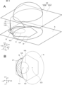
- FIG. 12A is a perspective view for explaining an example of a display device according to the third embodiment.
- FIG. 12B is a plan view for explaining an example of the display device according to the third embodiment.
- FIG. 12A is a perspective view for explaining an example of a display device according to the third embodiment.
- FIG. 12B is a plan view for explaining an example of the display device according to the third embodiment.
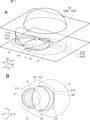
- FIG. 13A is a perspective view for explaining an example of a display device according to the third embodiment.
- FIG. 13B is a plan view for explaining an example of the display device according to the third embodiment.
- FIG. 14 is a cross-sectional view for explaining an example of the display device according to the fourth embodiment.
- FIG. 15 is a cross-sectional view for explaining an example of the display device according to the fifth embodiment.
- FIG. 16 is a plan view for explaining an example of the display device according to the sixth embodiment.
- FIG. 17A is a perspective view for explaining an example of a display device according to the sixth embodiment.
- FIG. 17B is a plan view for explaining an example of the display device according to the sixth embodiment.
- FIG. 18 is a plan view for explaining an example of a display device according to Modification 1 of the sixth embodiment.
- FIG. 19 is a plan view for explaining an example of optical simulation.
- FIG. 20A, FIG. 20B, and FIG. 20C are diagrams for explaining the results of optical simulation.
- 21A and 21B are diagrams for explaining an example of a display device having a resonator structure.
- 22A and 22B are diagrams for explaining an example of a display device having a resonator structure.
- 23A and 23B are diagrams for explaining an example of a display device having a resonator structure.
- FIG. 24 is a diagram for explaining an example of a display device having a resonator structure.
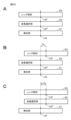
- 25A, 25B, and 25C are diagrams for explaining an example in which a display device has a wavelength selection section.
- FIG. 20A, FIG. 20B, and FIG. 20C are diagrams for explaining the results of optical simulation.
- 21A and 21B are diagrams for explaining an example of a display device having a resonator structure.
- 22A and 22B are diagrams for explaining
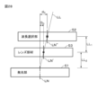
- FIG. 26 is a diagram for explaining an example in which the display device has a wavelength selection section.
- FIGS. 27A and 27B are diagrams for explaining an example in which a display device has a wavelength selection section.
- FIG. 28 is a diagram for explaining an example in which a display device has a wavelength selection section.
- 29A and 29B are diagrams for explaining an example of application of the display device.
- FIG. 30 is a diagram for explaining an example of application of the display device.
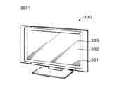
- FIG. 31 is a diagram for explaining an example of application of the display device.
- FIG. 32 is a diagram for explaining an example of application of the display device.
- FIG. 33 is a diagram for explaining an example of application of the display device.
- 34A and 34B are diagrams for explaining an example of application of the display device.
- Example 9 where the display device has a resonator structure.
- Example 10 of positional relationship when the display device has a wavelength selection section.
- the Z-axis direction is the vertical direction (the upper side is the +Z direction, the lower side is the -Z direction), the X-axis direction is the left-right direction (the right side is the +X direction, the left side is the -X direction), and the Y axis direction is the It is assumed that is the front-rear direction (the rear side is the +Y direction and the front side is the -Y direction), and the explanation will be based on this. This also applies to FIGS. 3 to 34.
- the relative size and thickness ratios of the layers shown in FIG. 1 and other figures are for convenience only, and do not limit the actual size ratios. The rules regarding these directions and the size ratios are the same for each of the figures from FIGS. 2 to 34.
- the display device 10 includes a plurality of pixels arranged two-dimensionally.
- one pixel may be formed by a combination of a plurality of sub-pixels 101.
- the following description will continue using an example in which one pixel in the display device 10 is formed by a combination of a plurality of sub-pixels corresponding to a plurality of color types. Note that in this case, a plurality of sub-pixels 101 are two-dimensionally arranged in the display device 10.
- FIG. 1 is a cross-sectional view showing one embodiment of a display device 10.
- FIG. 2A is a plan view showing an example of the display device 10.
- FIG. 2B is a diagram schematically showing an enlarged view of region XS1 in FIG. 2A. Note that in FIG.
- the light emitting part K is indicated by a region surrounded by a broken line, and the color filter is divided into color types by hatched regions.
- the top emission method refers to a method in which the light emitting element 104 is arranged closer to the display surface DP than the substrate 11A. Therefore, in the display device 10, the substrate 11A is located on the back side of the display device 10, and the direction (+Z direction) from the substrate 11A toward the light emitting element 104, which will be described later, is the front side (top side) of the display device 10. . In the display device 10, light generated from the light emitting element 104 is directed in the +Z direction and emitted to the outside.
- the surface that is the display surface side in the display area (display area 10A) of the display device 10 is referred to as a first surface (top surface), and the back surface side of the display device 10 is referred to as a first surface (top surface).
- the surface that becomes the second surface (lower surface) is called the second surface (lower surface). Note that this does not prohibit the case where the display device 10 according to the present disclosure is of a bottom emission type.
- the display device 10 can also be applied with a bottom emission method. In the bottom emission method, light generated from the light emitting element 104 is directed in the -Z direction and emitted to the outside.
- Type of subpixel In the examples shown in FIGS. 1, 2A, 2B, etc., three colors, red, green, and blue, are defined as a plurality of color types corresponding to the emitted light color of the display device 10, and the subpixels are a subpixel 101R and a subpixel 101G. , sub-pixel 101B are provided.
- the subpixel 101R, the subpixel 101G, and the subpixel 101B are a red subpixel, a green subpixel, and a blue subpixel, respectively, and display red, green, and blue, respectively.
- the example in FIG. 1 is just an example, and the display device 10 is not limited to having a plurality of subpixels corresponding to three color types.
- the wavelengths of light corresponding to each color type of red, green, and blue are, for example, in the range of 610 nm to 650 nm (red wavelength band), the range of 510 nm to 590 nm (green wavelength band), and the range of 440 nm to 480 nm, respectively. It can be defined as a wavelength in the (blue wavelength band).
- the number of subpixel color types is not limited to the three colors shown here, but may be two colors, four colors, etc.
- the color type of the subpixel is not limited to red, green, or blue, but may be yellow, white, or the like.
- the layout of the sub-pixels 101B, 101R, and 101G in the display device 10 is not particularly limited, but in the examples shown in FIGS. 1, 2A, and 2B, one pixel is The constituent sub-pixels 101B, 101R, and 101G are arranged in a delta shape, and each pixel is arranged in a two-dimensional layout. Therefore, in the display device 10 shown in the example of FIG. 1, a plurality of subpixels 101B, 101R, and 101G corresponding to a plurality of color types are provided in a two-dimensional delta-shaped layout.
- the delta-shaped layout refers to a layout in which a triangle is formed by line segments connecting the centers of a plurality of sub-pixels 101 forming a pixel. Note that FIG. 1 is an example, and as described later, the layout of the sub-pixels 101B, 101R, and 101G is not limited in this disclosure.
- 2A and 2B are diagrams for explaining examples of the display area 10A and sub-pixels 101 of the display device 10.
- the subpixels 101R, 101G, and 101B are collectively referred to as the subpixel 101 unless the types of the subpixels 101R, 101G, and 101B are particularly distinguished.
- the main optical axis L of the sub-pixel 101 near the center position CT of the display area 10A are different from the outer peripheral edge SL of the display area 10A and the main optical axis L of the sub-pixel 101 in the vicinity thereof.
- the main optical axis L of each of the plurality of sub-pixels 101 when the main optical axis L of each of the plurality of sub-pixels 101 is determined from a position close to the center of the display area 10A toward the outer peripheral edge SL of the display area 10A, , the main optical axis L of the sub-pixel 101 gradually changes from a position close to the center position CT of the display area 10A toward the outer peripheral edge SL. More specifically, in at least a portion of the display area 10A, the closer the subpixel 101 is disposed to the outer peripheral edge SL of the display area 10A, the more the main optical axis L of the subpixel 101 is inclined toward the outside. . In the example of FIG.
- the main optical axis L of each of the plurality of sub-pixels 101 is sequentially determined from the center position CT of the display area 10A toward the outer peripheral edge SL of the display area 10A (in the direction of arrow F (+X direction)).
- the main optical axes L(0), L(1), L(2 )...L(K), L(K+1), L(K+2)... are tilted ( fallen) in the direction of arrow F (however, K is a positive integer).
- the inclination of the main optical axis L(K+1) is greater than the inclination of the main optical axis L(K).
- the main optical axis L of the sub-pixel 101 is inclined from the center position CT toward the outer peripheral edge SL with reference to the thickness direction (Z-axis direction) of the light emitting element 104, the main optical axis L of the sub-pixel 101 is This is called the case where the direction is diagonal.
- the magnitude of the inclination of the principal optical axis L indicates the magnitude of the angle ⁇ between the Z-axis direction and the principal optical axis L, as shown in FIGS. 1, 10, etc.
- the greater the inclination of the main optical axis L the closer the main optical axis L becomes to the horizontal.
- FIG. 1 the greater the inclination of the main optical axis L
- the main optical axis L (the optical central axis, generally the radiation direction of the highest luminous intensity) of the sub-pixel 101 gradually changes from a position close to the center position CT of the display area 10A toward the outer peripheral edge SL.
- the case where the main optical axis L of the sub-pixel 101 gradually changes in units of one sub-pixel 101 is such that the direction of the emitted light gradually changes in units of one sub-pixel 101. It is not limited to cases where For example, a combination of a plurality of sub-pixels 101 from a position close to the center position CT of the display area 10A toward the outer peripheral edge SL is considered as one unit (first unit), and the sub-pixels are formed in that unit (with the first unit as a reference).
- the main optical axis L of 101 may change gradually.
- the sub-pixels 101 constituting the first unit have their principal optical axes L aligned in the same direction, and are specified at different positions.
- the principal optical axis L may gradually change from a position close to the center position CT of the display area 10A toward the outer peripheral edge SL.
- the principal optical axis L of the sub-pixel 101 gradually changes in the second unit, where a plurality of combinations of pixels (combination of a plurality of pixels) of the plurality of sub-pixels 101 is defined as one unit (second unit). You can.
- the directions of the main optical axes L are aligned, Regarding the relationship between the principal optical axes L corresponding to the second units specified at mutually different positions, the principal optical axis L gradually changes from a position close to the center position CT of the display area 10A toward the outer peripheral edge SL. good.
- the display device 10 generally includes a control circuit 107, an H driver 105, and a V driver 106, as illustrated in FIG. 2A, and the control circuit 107 controls driving of the H driver 105 and V driver 106. .
- the H driver 105 and the V driver 106 control driving of the subpixel 101 on a column-by-column basis and on a row-by-row basis, respectively.
- the subpixel 101 has a light emitting part K, and at least the light emitting part K has a light emitting element 104.
- the display device 10 includes a light emitting element 104 above the drive substrate 11.
- the light emitting element 104 has a structure in which a first electrode 13, an organic layer 14, and a second electrode 15 are laminated in this order above the drive substrate 11, as will be described later.
- FIG. 1 schematically shows a cross-sectional state of the display device 10 in a portion of the sub-pixel 101 where the main optical axis L is inclined.
- the driving substrate 11 includes an insulating layer 11B provided on a substrate 11A, and various circuits for driving a plurality of light emitting elements 104 are provided in the insulating layer 11B.
- various circuits include a drive circuit that controls driving of the light emitting elements 104 and a power supply circuit that supplies power to the plurality of light emitting elements 104 (none of which are shown). The various circuits are prevented from being exposed to the outside by the insulating layer 11B.
- the drive substrate 11 is provided with wiring for connecting the light emitting element 104 and the circuits provided on the substrate 11A to the first electrodes 13 and the like. Examples of the wiring include a plurality of contact plugs 11C.
- the substrate 11A may be made of, for example, glass or resin with low moisture and oxygen permeability, or may be made of a semiconductor with which transistors and the like can be easily formed.
- the substrate 11A may be a glass substrate, a semiconductor substrate, a resin substrate, or the like.
- the insulating layer 11B is made of, for example, an organic material or an inorganic material.
- the organic material includes, for example, at least one of polyimide and acrylic resin.
- the inorganic material includes, for example, at least one of silicon oxide, silicon nitride, silicon oxynitride, and aluminum oxide.
- a plurality of light emitting elements 104 are provided on the first surface side of the drive substrate 11.
- the light emitting element 104 is an organic electroluminescent element (organic EL element).
- organic EL element organic electroluminescent element
- the plurality of light emitting elements 104 light emitting elements are provided that emit light from the light emitting surface in a color corresponding to the color type of the subpixel 101 (as the emitted light color).
- light emitting elements 104R, 104G, and 104B are formed in subpixels 101R, 101G, and 101B, respectively.
- the plurality of light emitting elements 104 have a layout corresponding to the arrangement of the sub-pixels 101 of each color type.
- the plurality of light emitting elements 104 are two-dimensionally arranged in a delta-like arrangement pattern.
- the light emitting element 104 has a laminated structure in which a first electrode 13, an organic layer 14, and a second electrode 15 are laminated in this order.
- the first electrode 13, the organic layer 14, and the second electrode 15 are stacked in this order from the drive substrate 11 side in a direction from the second surface to the first surface.
- a plurality of first electrodes 13 are provided on the first surface side of the drive substrate 11.
- the first electrode 13 is an anode electrode.
- the first electrode 13 is composed of at least one of a metal layer and a metal oxide layer.
- the first electrode 13 may be composed of a single layer of a metal layer or a metal oxide layer, or a laminated film of a metal layer and a metal oxide layer.
- the metal layer examples include chromium (Cr), gold (Au), platinum (Pt), nickel (Ni), copper (Cu), molybdenum (Mo), titanium (Ti), tantalum (Ta), and aluminum (Al). , magnesium (Mg), iron (Fe), tungsten (W), and silver (Ag).
- the metal layer may contain the at least one metal element described above as a constituent element of an alloy. Specific examples of alloys include aluminum alloys and silver alloys. Specific examples of aluminum alloys include AlNd and AlCu.
- the metal oxide layer includes, for example, at least one of a mixture of indium oxide and tin oxide (ITO), a mixture of indium oxide and zinc oxide (IZO), and titanium oxide (TiO).
- ITO indium oxide and tin oxide
- IZO indium oxide and zinc oxide
- TiO titanium oxide
- the first electrode 13 is electrically isolated for each subpixel 101. That is, a plurality of first electrodes 13 are provided on the first surface side of the drive substrate 11 and are provided for each subpixel 101.
- an insulating layer (inter-pixel insulating layer) be formed between adjacent first electrodes 13.
- An interpixel insulating layer is formed between adjacent first electrodes 13.
- the inter-pixel insulating layer may be a layer formed of the same material as the insulating layer 11B, or may be a layer formed of a different material from the insulating layer 11B.
- the inter-pixel insulating layer is the same as the insulating layer 11B and is integrated with the insulating layer 11B, so for convenience of explanation, the inter-pixel insulating layer is not shown.
- the inter-pixel insulating layer will be described below using the term insulating layer 11B. In the example shown in FIG.
- the insulating layer 11B electrically isolates each first electrode 13 for each light emitting element 104 (that is, for each subpixel 101). Further, as shown in FIG. 1, an opening 12 is formed in the insulating layer 11B on the first surface side, and the opening 12 is formed on the first surface side of the first electrode 13 (the surface facing the second electrode 15). ) is exposed from the opening 12, and the portion of the first electrode 13 exposed from the opening 12 faces an organic layer 14, which will be described later, avoiding the interposition of the insulating layer 11B.
- the portion of the first electrode 13 exposed from the opening 12 and the organic layer 14 of the light emitting element 104 are The portion where the two face each other without intervening the insulating layer 11B is defined as the light emitting portion K.
- the insulating layer 11B may be formed not only between adjacent first electrodes 13 but also on the edge of the first electrodes 13.
- the edge of the first electrode 13 is defined by a portion from the outer peripheral edge of the first electrode 13 to a predetermined position closer to the center of the first electrode 13.
- the insulating layer 11B has the opening 12, and the first surface of the first electrode 13 is exposed from the opening 12.
- Organic layer 14 is provided on first electrode 13 .
- the organic layer 14 is provided at least between the first electrode 13 and the second electrode 15.
- a common layer may be employed regardless of the color type of the sub-pixel 101, or different layers may be employed.
- the organic layer 14 is common to the sub-pixels 101.
- the organic layer 14 is common to the subpixels 101R, 101G, and 101B, and is configured to be able to emit white light, for example. However, this does not prohibit the emission color of the organic layer 14 from being a color other than white, and colors such as red, blue, and green may be employed. That is, the emission color of the organic layer 14 may be, for example, any one of white, red, blue, and green.
- the organic layer 14 has, for example, a structure in which a hole injection layer, a hole transport layer, a light emitting layer, and an electron transport layer are stacked in this order from the first electrode 13 to the second electrode 15.
- An electron injection layer may be provided between the electron transport layer and the second electrode 15.
- the electron injection layer is for increasing electron injection efficiency. Note that the structure of the organic layer 14 is not limited to this, and layers other than the light emitting layer may be provided as necessary.
- the hole injection layer is a buffer layer for increasing the efficiency of hole injection into the light emitting layer and suppressing leakage.
- the hole transport layer is for increasing hole transport efficiency to the light emitting layer.
- the electron transport layer is for increasing the efficiency of electron transport to the light emitting layer.
- the light-emitting layer generates light by recombining electrons and holes by applying an electric field.
- the light emitting layer is an organic compound layer containing an organic light emitting material.
- a second electrode 15 is provided above the organic layer 14 .
- the second electrode 15 is provided as a common electrode for the plurality of subpixels 101.
- the second electrode 15 is a cathode electrode.
- the second electrode 15 is preferably a transparent electrode that is transparent to the light generated in the organic layer 14 .
- the transparent electrode herein includes one formed of a transparent conductive layer and one formed of a structure having a transparent conductive layer and a semi-transparent reflective layer.
- a transparent conductive material with good light transmittance and a small work function is preferably used for the transparent conductive layer.
- the transparent conductive layer can be formed of, for example, a metal oxide.
- the material for the transparent conductive layer is at least one of a mixture of indium oxide and tin oxide (ITO), a mixture of indium oxide and zinc oxide (IZO), and zinc oxide (ZnO). Examples include those containing seeds.
- the semi-transparent reflective layer can be formed of a metal layer, for example.
- the material of the transflective layer includes at least one metal element selected from the group consisting of magnesium (Mg), aluminum (Al), silver (Ag), gold (Au), and copper (Cu).
- Mg magnesium
- Al aluminum
- Au gold
- Cu copper
- the metal layer may contain the at least one metal element described above as a constituent element of an alloy. Specific examples of the alloy include MgAg alloy, AgPdCu alloy, and the like.
- the laminated structure 155 in which a plurality of layers are stacked is formed above the light emitting element 104.
- the laminated structure 155 includes a protective layer 16, a color filter 18, and a sealing resin layer 19. Note that, as shown in FIG. 1, the laminated structure 155 preferably has a flattening layer 17 between the protective layer 16 and the color filter 18. As will be described later, the subpixel 101 is provided with the structure 21 inside the stacked structure 155.
- the protective layer 16 is formed to cover the first surface of the light emitting element 104.
- the protective layer 16 makes it difficult for the first surface of the light emitting element 104 to come into contact with the outside air, and suppresses moisture from entering the light emitting element 104 from the external environment.
- the protective layer 16 is formed of an insulating material.
- the insulating material for example, thermosetting resin can be used.
- SiO, SiON, AlO, TiO, etc. may be used as the insulating material.
- the protective layer 16 can be exemplified by a CVD film containing SiO, SiON, etc., or an ALD film containing AlO, TiO, SiO, etc.
- the CVD film refers to a film formed using chemical vapor deposition.
- the ALD film refers to a film formed using atomic layer deposition.
- the protective layer 16 may be formed of a single layer or may have a structure in which a plurality of layers are laminated.
- the protective layer 16 may have a structure in which a CVD film and an ALD film are stacked.
- a planarization layer 17 is provided on the first surface of the protective layer 16.
- layers such as the color filter 18 can be formed on the first surface side of the flattening layer 17 with high precision.
- the material for forming the flattening layer 17 include ultraviolet curing resins and thermosetting resins. It is preferable that the planarizing layer, together with the protective layer 16, has the function of insulating the light emitting element 104 from the outside air and suppressing moisture intrusion into the light emitting element 104 from the external environment.
- a color filter 18 is provided on the flattening layer 17 on the first surface side (upper side, +Z direction side) of the protective layer 16.
- An example of the color filter 18 is an on-chip color filter (OCCF).
- the color filter 18 is provided according to the color type of the sub-pixel 101.
- the color filters 18 can include, for example, a red color filter (red filter 18R), a green color filter (green filter 18G), and a blue color filter (blue filter 18B).
- the red filter 18R, the green filter 18G, and the blue filter 18B are provided in the subpixels 101R, 101G, and 101B, respectively.
- the color filter 18 By providing the color filter 18 in the display device 10, light corresponding to the color types of the sub-pixels 101R, 101G, and 101B can be effectively extracted to the outside. Note that in the case where the organic layer 14 is formed to emit different colors for each color type of the sub-pixel 101, the color filter 18 may be omitted.
- the thickness direction (Z-axis direction) of the light emitting element 104 when the thickness direction (Z-axis direction) of the light emitting element 104 is taken as the viewing direction, as shown in FIG. 1, the center C2 of the color filter 18 and It is preferable that the center C1 of the light emitting part K is shifted.
- the thickness direction (Z-axis direction) of the light-emitting element 104 is taken as the line-of-sight direction
- the direction in which the center C2 of the color filter 18 and the center C1 of the light-emitting part K are shifted corresponds to the direction in which the main optical axis L is inclined.
- the center of the color filter and the center of the light emitting part roughly coincide with each other near the center of the display area.
- the center C1 and the center C2 approximately coincide, and the -X direction and +X direction from the center position CT.
- the sub-pixel 101 that is set at an outer position (a position away from the center position CT) along The main optical axis L is inclined.
- structures 21 are provided in at least some of the subpixels 101.
- the structure 21 controls the traveling direction of at least a portion of the light W generated from the light emitting element 104.
- the structure 21 arranged in the subpixel 101 is an optical member that bends at least part of the light generated from the light emitting element 104 in a direction corresponding to the main optical axis L of the subpixel 101.
- a specific example of the optical member is a lens.
- the structure 21 is a lens in the shape of a beveled cylinder.
- the structure 21 is preferably formed in the subpixel 101 having the main optical axis L inclined in an oblique direction.
- the structure 21 in such a sub-pixel 101, out of the light W generated from the light emitting element 104, the light traveling in the thickness direction (Z-axis direction) of the light emitting element 104 passes through the structure 21.
- the direction of the output light WR from the structure body 21 can be tilted in an oblique direction, so that it is easy to direct the output light WR toward the main optical axis L of the sub-pixel 101.
- the structure 21 is formed inside a stacked structure 155.
- the sealing resin layer 19 is provided so as to cover the side surfaces 122 and top surface 121 of the structure 21, and the top surface 121 and side surface 122 of the structure 21 are in contact with the sealing resin layer 19.
- the structure 21 may be provided so as to be embedded inside the sealing resin layer 19 such that the bottom surface 123 thereof is in contact with the sealing resin layer 19.
- the structure 21 is arranged in a region including directly above at least a portion of the light emitting part K. By arranging the structure 21 in this way, it becomes easy to bend the light traveling from the light emitting portion K in the thickness direction of the light emitting element 104 toward the main optical axis L of the subpixel 101 by the structure 21. .
- the orthogonal projection of the structure 21 overlaps or covers at least a portion of the light-emitting part K.
- the orthogonal projection of the structure 21 indicates the orthogonal projection of the structure 21 onto a plane A with the thickness direction of the light emitting element 104 as the normal; that is, when the structure 21 is projected in parallel using the plane A as the projection plane. shows the projection recognized in The plane A is a plane whose plane direction is the XY direction as shown in FIGS. 12A and 13B, as shown in the third embodiment described later.
- the center of the color filter 18 is C2 and the center C1 of the light emitting part K are shifted from each other.
- the direction in which the center C2 of the color filter 18 and the center C1 of the light emitting part K are shifted is defined as the direction of misalignment
- the orthogonal projection of the structure 21 is in the formation area of the light emitting part K, with the center C1 of the light emitting part K being sandwiched therebetween. It is preferable to cover at least a part of the area on the side opposite to the direction of deviation.
- the structure 21 is obtained by cutting a columnar shape with an inclined surface in an oblique direction, as shown in FIGS. 1, 3A to 3C, 4A to 4C, 5A to 5C, 6A to 6C, etc. It is preferable that the top surface 121, the side surfaces 122, and the bottom surface 123 are configured to have a shape (referred to as a diagonal columnar shape) that can be recognized as follows.
- the inclined surface is not limited to a flat surface, but also includes a curved surface such as a cylindrical surface.
- the columnar shape is not particularly limited, and examples thereof include a columnar shape and an elliptical columnar shape. In FIGS. 3A, 4A, 5A, 6A, etc., the columnar shape is illustrated by a shape M indicated by a broken line.
- the upper surface 121 of the structure 21 is a surface that is recognized as a cut surface when a columnar shape is cut diagonally, and corresponds to a surface facing diagonally upward.
- the upper surface 121 is viewed from the structure 21 with the direction from the first surface to the second surface (-Z direction) along the thickness direction (Z-axis direction) of the light emitting element 104 as the viewing direction. This is the surface of the structure 21 that is generally recognized when
- the side surface 122 of the structure 21 is the side surface of the structure 21 that is observed when the structure 21 is viewed with the line of sight in the plane (XY plane) whose normal direction is the thickness direction of the light emitting element 104. Of these, surfaces excluding the top surface 121 and the bottom surface 123 are shown.
- the bottom surface 123 of the structure 21 refers to the end surface (opposite surface) opposite to the cut surface that is observed when cutting the columnar shape in an oblique direction. In the example of FIG. 1, the bottom surface 123 of the structure 21 is formed with the viewing direction from the second surface to the first surface (+Z direction) along the thickness direction (Z-axis direction) of the light emitting element 104. This is the surface of the structure 21 that can be seen when looking at 21.
- the structure 21 is formed into a diagonally cut columnar shape.
- the obliquely cut cylindrical shape refers to a shape that is observed when a cylindrical shape is cut with an inclined surface (a plane or a curved surface) in a diagonal direction with respect to the central axis of the cylinder.
- the term "slanted cylindrical shape” refers to cases in which a cylindrical shape is cut with an inclined surface (an inclined plane in FIG. 3A) so as not to cross the bottom surface of the cylindrical shape, as shown in FIGS. 3A to 3C; As shown in FIGS.
- the columnar shape is an elliptical columnar shape
- the structure 21 is formed in a diagonally cut elliptical columnar shape, as shown in FIGS. 5A to 5C and FIGS. 6A to 6C.
- the term "obliquely cut elliptical columnar shape” refers to a shape that is observed when an elliptical columnar shape is cut at a plane located at the center of the elliptical column and inclined to a line extending in the longitudinal direction of the columnar shape.
- FIGS. 3A, 4A, 5A, and 6A are perspective views showing one embodiment of the structure 21, and FIGS. 3B, 4B, 5B, and 6B are respectively FIGS. 3A, 4A, and 5A.
- FIG. 3C, FIG. 4C, FIG. 5C, and FIG. 6C are plan views of the structure 21 shown in FIG. 6A
- FIG. 3C, FIG. 4C, FIG. 5C, and FIG. 6B is a sectional view showing the state of the cross section taken along line CC in FIG. 5B and the state taken along the line DD in FIG. 6B.
- position C4 indicates the center of gravity of the structure 21 (the position of the center of gravity in the orthogonal projection of the structure 21).
- the shape and outline of the upper surface 121 of the structure 21 are preferably such that when the columnar shape is cut diagonally, the shape and outline are recognized as a cut surface.
- the slope of the upper surface 121 of the structure 21 is preferably determined such that the normal direction of the upper surface 121 of the structure 21 is the direction of the main optical axis L of the sub-pixel 101.
- the normal direction of the upper surface 121 of the structure 21 refers to the normal direction at the center of the upper surface 121.
- the normal direction of the upper surface 121 of the structure 21 can be set as the central axis of curvature (the axis of symmetry of curvature) at the center of the upper surface 121.
- the slope of the top surface 121 of the structure body 21 is determined so that the normal direction of the top surface 121 of the structure body 21 becomes the main optical axis L of the subpixel 101, light emitted from the light emitting element 104 according to the subpixel 101 is Control of the traveling direction of at least some of the generated light W can be adjusted. Therefore, the possibility that the light W traveling outward from the light emitting portion K of the subpixel 101 along the thickness direction of the light emitting element 104 is removed from the subpixel 101 and leaks to the adjacent subpixel 101 side is efficiently suppressed. be able to.
- the slope of the top surface 121 of the structure 21 can be determined depending on conditions such as the height H of the structure 21 and the size of the bottom surface 123 shown in FIG. 3 and the like.
- the upper surface 121 of the structure 21 is formed in a planar shape in the example shown in FIG. 1 and the like, the upper surface 121 is not limited to this. As illustrated in FIGS. 7A to 7C, the upper surface 121 of the structure 21 may have a curved surface corresponding to a part of the spherical surface (partial spherical surface).
- 7A is a perspective view showing an example of the structure 21
- FIG. 7B is a plan view of the structure 21 shown in FIG. 7A
- FIG. 7C is a cross-sectional view taken along line EE in FIG. 7B.
- the material of the structure 21 is not particularly limited as long as it can transmit light, but examples thereof include resin materials such as ultraviolet curing resin and thermosetting resin.
- the refractive index (N1) of the structure 21 is smaller than the refractive index of the adjacent portion 156.
- the refractive index N1 of the structure 21 is smaller than the refractive index (N2) of the sealing resin layer 19 (N1 ⁇ N2). Since the refractive index of the structure 21 is smaller than the refractive index of the adjacent portion 156, the light W traveling from the light emitting element 104 inside the structure 21 is When the emitted light WR is made to travel outward from the upper surface 121 etc. of the structure 21, the emitted light WR is made to travel in the direction toward the main optical axis L of the sub-pixel 101 or in the direction along the main optical axis L. , it becomes easy to refract the light W.
- the top surface of the structure 21 is It is preferable that the direction of the emitted light WR from 121 gradually changes.
- the direction of the emitted light WR from the upper surface 121 of the structure 21 referred to here refers to the light along the main optical axis LW (the direction in which the light intensity is maximum) for the emitted light WR from the upper surface 121 of the structure 21.
- the layout of the structure 21 is formed not only in one direction of the display area 10A but also in all directions from the center position CT of the display area 10A along the surface direction (XY plane direction) of the display area 10A.
- the structure 21 is not shown, and an example of the direction of the emitted light WR and the main optical axis LW is shown.
- the direction of the emitted light WR from the upper surface 121 of the structure 21 (the direction of the main optical axis LW) is It is preferable that the structures 21 provided in the sub-pixels 101 located closer to the outer peripheral edge SL of the region 10A are more inclined toward the outside. Also in the layout of such a structure 21, it is preferable that the structures are formed not only in one direction of the display area 10A but also in all directions from the center position CT of the display area 10A along the surface direction of the display area 10A. In this case, in all directions, the closer the sub-pixel 101 is disposed to the outer peripheral edge SL of the display area 10A, the easier it is to make the main optical axis L of the sub-pixel 101 obliquely inclined.
- Structures 21 provided in different subpixels 101 are separated from each other.
- the structure 21 provided in one subpixel 101 is arranged in a non-contact state with the structure 21 provided in another subpixel 101 adjacent to that subpixel 101. Since the structures 21 provided in different subpixels 101 are separated from each other, it becomes easy to suppress mixing of light between different subpixels 101.
- the display device 10 has an adjacent portion 156 as a layer (top contact layer) that is in contact with the top surface 121 of the structure 21 .
- the side surface 122 and the top surface 121 of the structure 21 are arranged inside the sealing resin layer 19, and since the top surface 121 of the structure 21 is in contact with the sealing resin layer 19, the adjacent portion 156 is a sealing resin layer 19.
- at least a portion of the bottom surface 123 of the structure 21 is in contact with the color filter 18.
- a sealing resin layer 19 is formed on the first surface side of the color filter 18 so as to cover the structure 21.
- the sealing resin layer 19 can exhibit a function of smoothing the surface of the first surface, which is the surface on which the color filter 18 is formed.
- the sealing resin layer 19 can have a function as an adhesive layer that adheres a counter substrate 20, which will be described later.
- the sealing resin layer 19 can be exemplified by ultraviolet curable resin, thermosetting resin, or the like.
- a counter substrate 20 may be provided on the first surface side of the sealing resin layer 19.
- the material of the counter substrate 20 the material of the substrate 11A of the drive substrate 11, etc. can be used.
- a glass substrate can be used as the counter substrate 20.
- the material of the glass substrate is not particularly limited, as long as it is made of a substance that allows light emitted from the organic layer 14 to pass therethrough.
- the material of the glass substrate include various glass substrates such as high strain point glass, soda glass, borosilicate glass, and lead glass, and quartz substrates.
- the method for manufacturing the display device 10 can be carried out, for example, as follows.
- a light emitting element 104 (first electrode, organic layer, and second electrode) is formed on the drive substrate 11. Furthermore, a protective layer 16, a planarization layer 17, and a color filter 18 are formed. Then, a structure 21 is formed.
- Examples of the method for forming the structure 21 include a method using a nanoimprint method as shown in FIGS. 8A to 8C, a method using a gray scale mask (3D photomask) and photolithography technology, etc.
- FIGS. 8A to 8C are diagrams for explaining a method of forming the structure 21 using the nanoimprint method.
- a layer 158 for forming the structure 21 is formed on the substrate 157 in which the light emitting element 104, the protective layer 16, the planarization layer 17, and the color filter 18 are formed on the driving substrate 11.
- the layer 158 can be formed of an ultraviolet curing resin or the like.
- a mold 159 corresponding to the shape of the structure 21 is placed above the layer 158. As shown in FIG.
- a mold 159 is pressed against the layer 158.
- the mold 159 has a light-transmitting structure, and by irradiating light P from the outside with the mold 159 pressed against the layer 158, the resin forming the layer 158 is shaped into the shape of the structure 21. Let it harden. As a result, a structure 21 is formed as shown in FIG. 8C.
- each of the driving substrate 11, light emitting element 104, protective layer 16, planarization layer 17, color filter 18, and sealing resin layer 19 described above is a method used in the manufacturing process of a general display device. May be used as appropriate.
- the manufacturing method shown here is an example, and the manufacturing method of the display device 10 is not limited thereto.
- the subpixel 101 is provided with the structure 21, and the structure 21 adjusts the traveling direction of the light W generated from the light emitting element 104 formed in the subpixel 101. .
- the structure 21 changes the traveling direction of the emitted light WR to the light W as shown in FIG. It can be directed toward the direction determined as the main optical axis L of the sub-pixel 101 compared to the traveling direction. Therefore, even if the main optical axis L of the sub-pixel 101 disposed near the outer peripheral edge SL of the display area 10A in the display device 10 is inclined outward, the structure 21 is attached to the sub-pixel 101.
- the structure 21 is configured to bend the traveling direction of the light W in the direction of the main optical axis L, so that the sub-pixel is arranged near the outer peripheral edge SL of the display area 10A. It becomes possible to improve the brightness loss at 101.
- the structures 21 provided in the subpixel 101 are independent of each other, so that the structure 21 provided in the subpixel 101 is the same as that of the subpixel adjacent to the subpixel 101. Mixing of light caused by taking in the light generated in step 101 can be suppressed. In particular, when the color types between adjacent sub-pixels 101 are different, color mixture can be suppressed.
- the layout of the subpixels 101B, 101R, and 101G is not limited to the delta shape.
- the layout of the sub-pixels 101B, 101R, and 101G may be a square arrangement or a sprite-like arrangement.
- Modification 2 In the example of the display device 10 according to the first embodiment shown in FIG. A first laminated substrate and a second laminated substrate in which a light emitting element 104 and a protective layer 16 are formed on a driving substrate 11 are prepared, and a planarizing layer 17 is applied to the first laminated substrate and a second laminated substrate. It is also possible to adhere the material through the adhesive.
- FIG. 9 is a cross-sectional view showing an example of the display device 10 according to the second embodiment.
- a laminated structure 155 is formed on the light emitting element 104 as in the first embodiment, and the laminated structure 155 has the following structure.
- a protective layer 16 is included.
- the protective layer 16 may be the same as the protective layer according to the first embodiment except that the structure 21 is formed therein. Therefore, the material of the protective layer 16 may be formed of the same insulating material as the protective layer shown in the display device 10 according to the first embodiment.
- the display device 10 has the structure 21 disposed inside the protective layer 16 as described above.
- the adjacent portion 156 is the protective layer 16.
- the structure 21 may be configured in the same manner as shown in the first embodiment except that it is embedded inside the protective layer 16.
- the orthogonal projection, shape, and layout of the structure 21 in the second embodiment may be the same as those in the first embodiment. It is also similar to the first embodiment that the structures provided in different subpixels are separated from each other.
- the refractive index N1 of the structure 21 is smaller than the refractive index of the adjacent portion 156, as in the first embodiment.
- the refractive index N1 of the structure 21 is smaller than the refractive index (N3) of the protective layer 16 (N1 ⁇ N3). It is.
- a structure in which the structure 21 is buried inside the protective layer 16 can be formed, for example, as follows.
- the first layer is partially formed as part of the protective layer 16.
- a structure 21 is formed on the first layer.
- a method for forming the structure 21 a method similar to the manufacturing method described in the first embodiment can be adopted.
- a second layer is formed as a part of the protective layer 16 (a portion other than the first layer), thereby forming a structure in which the structure 21 is embedded in the protective layer 16.
- the case where the color filter 18 is an OCCF is illustrated, but as explained in the first embodiment, the sealing resin layer 19 and the color filter 18 are provided on the counter substrate 20.
- the formed first multilayer substrate and a second multilayer substrate in which the light emitting element 104 and the protective layer 16 are formed on the drive substrate 11 are prepared, and the first multilayer substrate and the second multilayer substrate are coated with a planarization layer 17. It is also possible to adhere the material through the adhesive.
- FIG. 10 is a sectional view showing an example of the display device 10 according to the third embodiment. Although the sealing resin layer 19 and the counter substrate 20 are shown in FIG. 10, the sealing resin layer 19 and the counter substrate 20 are shown for convenience of explanation in FIGS. Omitted.
- the lens layer 22 is formed of a base layer 22A and a plurality of lenses 22B formed on the first surface of the base layer 22A.
- the lens 22B is preferably an on-chip lens (OCL).
- OCL on-chip lens
- the material of the lens 22B is not particularly limited, and various materials such as a resin material that can be used when forming the flattening layer 17, the sealing resin layer 19, etc. described in the first embodiment may be used. can.
- the base layer 22A forms a portion connected to the base end of the lens 22B.
- the base layer 22A may be made of the same material as the lens 22B.
- the base layer 22A may be formed integrally with the lens 22B.
- the base layer 22A is formed integrally with the lens 22B, and for convenience of explanation, the base layer 22A and the lens 22B are shown with the same hatching, and the boundary line between the base layer 22A and the lens 22B is shown as a broken line. has been done.
- each lens 22B forming the lens layer 22 is preferably formed in a convex shape having a curved surface convexly curved in a direction away from the drive substrate 11 (+Z direction). It is preferable that the lens be a so-called convex lens.
- the lens layer 22 is configured as a portion having a structure having a plurality of convex lenses on the base layer 22A.
- the lens 22B is formed at a position corresponding to each sub-pixel 101.
- the center C3 of the lens 22B and the center C1 of the light emitting part K are shifted from each other in the subpixel 101 whose main optical axis L is defined in an oblique direction.
- a part of the formation area of the light emitting part K may vary depending on the magnitude of the deviation between the center C3 of the lens 22B and the center C1 of the light emitting part K. It is out of the formation area of the lens 22B.
- the light-emitting part K and the lens 22B in the sub-pixel 101 formed at the center position CT of the display area 10A are connected to the center C3 of the lens 22B and the light-emitting part K
- the centers C1 of the light emitting elements 104 are generally coincident with each other, and when the thickness direction of the light emitting element 104 is taken as the line of sight direction, the formation area of the light emitting part K is formed inside the formation area of the lens 22B.
- FIG. 11 is a plan view showing an example of the layout of the positional relationship between the lens 22B, the color filter 18, and the light emitting part K in the sub-pixel 101.
- illustration of other layer structures for example, the sealing resin layer 19, etc.
- the direction in which the center C3 of the lens 22B and the center C1 of the light emitting section K are shifted is a direction corresponding to the direction in which the main optical axis L of the sub-pixel 101 is inclined.
- the direction in which the main optical axis L of the sub-pixel 101 is inclined is also generally in the +X direction. It is preferable that the In the display device 10 according to the third embodiment, at least some of the sub-pixels 101 move from the sub-pixels 101 near the center position CT of the display area 10A toward the sub-pixels 101 near the outer peripheral edge SL of the display area 10A.
- FIG. 10 shows a cross section of a portion of the subpixel 101 formed in the display device 10, the subpixel 101 having its main optical axis L determined in an oblique direction.
- the display device 10 has a structure 21 disposed on the color filter 18.
- the upper surface 121 and side surface 122 of the structure 21 and the first surface side portion of the color filter 18 are covered with the lens layer 22, and the upper surface 121 of the structure 21 is in contact with the lens layer 22. Therefore, the adjacent portion 156 becomes the lens layer 22.
- the adjacent portion 156 becomes the lens layer 22.
- the display device 10 shown in FIG. 10 is an example, and the case where the structure body 21 is embedded inside the lens layer 22 is not prohibited.
- the structure in which the structure 21 is buried inside the base layer 22A of the lens layer 22 is formed using the same method as the method in which the structure 21 is buried inside the protective layer 16 in the second embodiment. can do.
- a part of the base layer 22A is partially formed on the color filter 18.
- a structure 21 is formed on that layer.
- a layer that will become the remaining part of the base layer 22A is formed to cover the structure 21, thereby embedding the structure 21 in the portion of the lens layer 22 that corresponds to the base layer 22A.
- a structure is formed.
- the structure 21 is formed on the color filter 18 (on the first surface).
- the method for forming the structure 21 can be the same as the method described in the manufacturing method shown in the first embodiment.
- the structure 21 is configured to have a shape that is recognized when a columnar shape is cut diagonally, as shown in FIG. 10, as in the first embodiment.
- the structure 21 is formed in the shape of a diagonally cut column.
- the structure 21 preferably has a shape corresponding to the outer shape of the lens 22B, as shown in FIGS. 12A and 12B.
- the lens 22B has a hemispherical shape or a partially spherical shape, it is preferable that the structure is formed into a diagonally cylindrical shape.
- the structure 21 is formed in the shape of a diagonally cut elliptical column, as shown in FIGS. 13A and 13B. In the example of FIG. 10, the structure 21 is formed into a diagonally cut cylindrical shape.
- the orthogonal projection Q of the structure 21 onto A covers at least a part of the formation area KA of the light emitting part K and is outside the formation area R of the lens 22B.
- the orthogonal projection Q of the structure 21 has a shape that covers the area outside the formation area R of the lens 22B in the formation area KA of the light-emitting part K. It is preferable to have.
- the orthogonal projection Q of the structure 21 is the formation area of the lens 22B in the formation area KA of the light emitting part K, as shown in FIGS. 12A and 12B. It is preferable to cover the entire region except for R.
- FIGS. 12A and 13B are a perspective view and a plan view showing an example of the positional relationship among the light emitting part K, the lens 22B, and the structure 21.
- the formation area CA of the color filter 18 is also described.
- the orthogonal projection Q on the plane A is shown by a hatched area.
- the thickness of the base layer 22A is omitted and is shown in accordance with the lens 22B.
- FIGS. 12A for convenience of explanation, FIGS.
- the above-mentioned formation area KA corresponds to an area determined by orthographic projection of the light emitting part K onto the plane A.
- the formation region R corresponds to the region determined by orthographic projection of the lens 22B onto the plane A.
- the formation area CA corresponds to an area determined by orthographic projection of the color filter 18 onto the plane A.
- the refractive index N1 of the structure 21 is preferably smaller than the refractive index of the adjacent portion 156, as in the first embodiment. Preferably, it is smaller than the ratio. In the example of FIG. 10, since the adjacent portion 156 is also the base layer 22A, it is preferable that the refractive index N1 of the structure 21 is smaller than the refractive index N4 of the base layer 22A (N1 ⁇ N4).
- the layout of the structure 21 is similar to the first embodiment.
- the main optical axis L of the subpixel 101 is inclined in an oblique direction (outward direction) as the subpixel 101 is disposed closer to the outer peripheral edge SL of the display area 10A.
- the direction of the emitted light WR from the upper surface 121 of the structure 21 (the main optical axis LW of the emitted light WR from the upper surface 121 of the structure 21) is arranged at a position close to the outer peripheral edge SL of the display area 10A. It is preferable that the sub-pixel 101 be inclined outward in line with the main optical axis L.
- the thickness direction of the light emitting element 104 when taken as the line of sight direction, a region outside the formation region R of the lens 22B out of the formation region KA of the light emitting part K as shown in FIGS. 12A and 12B.
- the main optical axis L of the sub-pixel 101 is larger, and the main optical axis L of the sub-pixel 101 is tilted more obliquely as the sub-pixel 101 is disposed closer to the outer peripheral edge SL of the display area 10A. is determined.
- the mutual arrangement of the structures 21 is the same as in the first embodiment, and the structures 21 are formed in each of at least some of the plurality of subpixels 101, and the structures 21 provided in different subpixels 101 are arranged in the same manner as in the first embodiment. , separated from each other.
- sealing resin layer is formed to cover the first surface of the lens layer 22 (not shown).
- the material of the sealing resin layer is the same as that of the sealing resin layer 19 described in the first embodiment.
- a counter substrate is disposed on the first surface side of the sealing resin layer, similarly to the first embodiment and the like.
- the optical member forming the structure 21 is a lens
- the subpixel 101 has a structure in which the lens as the structure 21 and the lens 22B are provided. (a structure provided with multiple types of lenses) is formed.
- the lens 22B is the first lens and the lens serving as the structure 21 is the second lens
- the light W traveling from the light emitting part K in the thickness direction of the light emitting element 104 is refracted when it passes through the second lens.
- the traveling direction of the emitted light WR that is refracted when passing through the second lens is directed toward the main optical axis L direction rather than the traveling direction of the light W.
- the emitted light WR can pass through the first lens, making it easier to advance the emitted light WRN (the emitted light that has passed through the lens 22B) along the main optical axis L direction.
- the orthogonal projection Q of the structure 21 is outside the formation region R of the lens 22B, so that the light traveling from the light emitting element 104 toward the lens 22B is not reflected by the structure 21. It is possible to move towards the lens 22B without changing the way of movement.
- FIG. 14 is a sectional view showing an example of the display device 10 according to the fourth embodiment.
- the protective layer 16 has a structure 21 formed therein.
- the material of the protective layer 16 is the same as that in the third embodiment, so its explanation will be omitted.
- the adjacent portion serves as a protective layer.
- the structure 21 may have the structure shown in FIG. 12A, FIG. 12B, FIG. 13A, or FIG. 13B, for example, similar to that shown in the third embodiment.
- the structure 21 is formed into a diagonally cut cylindrical shape.
- the material of the structure 21 in the protective layer 16 may be the same as that in the second embodiment.
- a method similar to the method described in the second embodiment may be applied.
- the orthogonal projection Q of the structure 21 is the same as in the third embodiment, as shown in FIGS. 12A, 12B, 13A, and 13B. It is preferable that it covers at least a portion of the lens 22B and is outside the formation region R of the lens 22B. Further, in one sub-pixel 101, it is preferable that the orthogonal projection Q of the structure 21 covers the entire area of the formation area KA of the light emitting part K except for the formation area R of the lens 22B.
- the refractive index N1 of the structure 21 is preferably smaller than the refractive index of the adjacent portion 156, as in the second embodiment. It is preferable that the ratio is smaller than N3 (N1 ⁇ N3).
- FIG. 15 is a cross-sectional view showing an example of the display device 10 according to the fifth embodiment.
- the third It has the same structure as the display device 10 according to the embodiment.
- the subpixel 101 similarly to the first to fourth embodiments, the subpixel 101 has a layered structure 155 in which a plurality of layers are formed above the light emitting element 104. is formed, and the structure 21 is provided inside the laminated structure 155.
- a plurality of structures 21 are provided inside the stacked structure 155 of one subpixel 101. .
- the configurations of the layer 22, the sealing resin layer 19, and the counter substrate 20 are the same as those in the third embodiment, and therefore, descriptions of these configurations will be omitted.
- the laminated structure 155 includes a lens layer 22, and the lens layer 22 has a plurality of lenses 22B similarly to the third embodiment.
- the top surface 121 of each of the plurality of structures 21 is in contact with a layer constituting the laminated structure 155 , but the layer in contact with the top surface 121 is between the plurality of structures 21 . It's different.
- a top surface 121A and a side surface 122A of a first structure 21A which will be described later, are in contact with a protective layer 16, and a portion 156 adjacent to the first structure 21A is the protective layer 16.
- a top surface 121B and a side surface 122B of the second structure 21B are in contact with the lens layer 22 (base layer 22A of the lens layer 22 in the example of FIG. 15), and an adjacent portion 156 to the second structure 21B is the lens layer 22 (base layer 22A in the example of FIG. 15).
- the bottom surface 123A of the first structure 21A is in contact with the protective layer 16, and at least a portion of the bottom surface 123B of the second structure 21B is in contact with the color filter 18.
- each sub-pixel 101 has a first structure 21A and a second structure with different adjacent parts 156 as the structure 21. 21B. Note that when the first structure 21A and the second structure 21B are not distinguished, they are simply referred to as structure 21.
- the first structure 21A is provided inside the protective layer 16.
- the first structure 21A may be formed similarly to the structure 21 described in the fourth embodiment.
- the second structure 21B is provided on the color filter 18.
- the second structure 21B may be formed similarly to the structure 21 described in the third embodiment.
- the center CA4 of the first structure 21A and the center CB4 of the second structure 21B are shifted from each other with the thickness direction (Z-axis direction) of the light emitting element 104 as the line of sight direction. It is preferable that the first structure 21A and the second structure 21B are disposed at.
- the center of the structure 21 (the center CA4 of the first structure 21A and the center CB4 of the second structure 21B) is located in the thickness direction of the light emitting element 104, as shown for the center C4 of the structure 21 in FIG. 3B etc.
- the position of the center of gravity of the structure 21 (the position of the center of gravity of the first structure 21A and the position of the center of gravity of the second structure 21B) is shown with (Z-axis direction) as the viewing direction.
- proximal structure As a plurality of structures formed in one subpixel, there are structures formed in a layer closer to the light emitting element and structures formed in a layer farther from the light emitting element. .
- a structure formed in a layer close to the light emitting element is called a proximal structure.
- the proximal structure is a structure whose adjacent portion is a layer close to the light emitting element.
- the first structure 21A is a structure 21 provided in a layer (protective layer 16) that is closer to the light emitting element 104 than the second structure 21B.
- the body 21A is the proximal structure.
- the orthogonal projection of the structure covers at least a part of the light emitting part formation area and is outside the lens formation area. It is preferable that In the example of the display device 10 according to the fifth embodiment shown in FIG. 15, the orthogonal projection of the first structure 21A is the orthogonal projection Q of the structure 21 shown in FIGS. 12A, 12B, 13A, and 13B. Similarly, it is preferable to cover at least a part of the formation area KA of the light emitting part K and to be outside the formation area R of the lens 22B.
- the layout of the plurality of structures 21 in which one of the layers forming the stacked structure 155 is the adjacent portion 156 may be the same as in the first to fourth embodiments.
- the layout of the first structure 21A may be similar to the second embodiment or the fourth embodiment.
- the layout of the second structure 21B may be similar to that of the third embodiment.
- the refractive index NA1 of the first structure 21A is smaller than the refractive index N3 of the protective layer 16 (NA1 ⁇ N3). It is preferable that the refractive index NB1 of the second structure 21B is smaller than the refractive index N4 of the base layer 22A (NB1 ⁇ N4).
- the optical member forming the structure 21 is a lens
- the sub-pixel 101 includes a lens as the first structure 21A and a second structure.
- a structure provided with a lens as the body 21B (a structure provided with a plurality of types of lenses) is formed.
- the lens 22B is a first lens
- the second structure 21B is a second lens
- the lens serving as the first structure 21A is a third lens
- the subpixel 101 whose main optical axis L is in an oblique direction emits light.
- light W traveling to a position away from the first lens can be taken into the third lens.
- the light W is refracted when passing through the third lens.
- the traveling direction of the emitted light WRA that is refracted when passing through the third lens is directed toward the main optical axis L direction rather than the traveling direction of the light W.
- the second lens is arranged closer to the first lens than the third lens, and the emitted light WRA can pass through the second lens to form the emitted light WRB.
- the emitted light WRB (the emitted light that has passed through the second lens) can be formed so as to proceed toward the first lens, which becomes the lens 22B.
- the emitted light WRB passes through the first lens, and it is possible to form the emitted light WRN directed further in the direction of the main optical axis L.
- a layered structure 155 formed above the light emitting element 104 includes a protective layer 16, a color filter 18, and a sealing resin layer 19, and is arranged inside the layered structure 155.
- the structure 21 includes a first structure 21A provided inside the protective layer 16 and a second structure 21B provided above the color filter 18.
- the upper surface 121B of the second structure 21B is in contact with the sealing resin layer 19, and the adjacent portion 156 to the second structure 21B becomes the sealing resin layer.
- FIG. 16 is a sectional view showing an example of the display device 10 according to the sixth embodiment.
- the example of the display device 10 according to the sixth embodiment shown in FIG. It has the same structure as the display device 10.
- the subpixel 101 has a layered structure 155 in which a plurality of layers are formed above the light emitting element 104. is formed, and the structure 21 is provided inside the laminated structure 155.
- a plurality of structures having the same adjacent portion 156 are provided inside the stacked structure 155 of one sub-pixel 101. 21 are provided.
- the configurations of the layer 22, the sealing resin layer 19, and the counter substrate 20 are the same as those in the third embodiment, and therefore, descriptions of these configurations will be omitted.
- the laminated structure 155 includes a lens layer 22, and the lens layer 22 has a plurality of lenses 22B similarly to the third embodiment.
- the layers in contact with the upper surfaces 121 of the plurality of structures 21 are the same layer among the layers constituting the laminated structure 155.
- Upper surfaces 121C and 121D of a third structure 21C and a fourth structure 21D which will be described later, are both in contact with the lens layer 22 (base layer 22A in the example of FIG. 16), and the adjacent portion 156 is Both the structure 21C and the fourth structure 21D serve as the base layer 22A.
- side surfaces 122C and 122D of the third structure 21C and the fourth structure 21D are also in contact with the base layer 22A. Note that at least a portion of the bottom surface 123C of the third structure 21C and at least a portion of the bottom surface 123D of the fourth structure 21D are in contact with the color filter 18.
- the third structure 21C and the fourth structure 21D are provided in each subpixel 101, as described above. have Note that when the third structure 21C and the fourth structure 21D are not distinguished, they are simply referred to as the structure 21.
- the third structure 21C is provided on the color filter 18 and is formed similarly to the structure 21 shown in the third embodiment.
- the shape of the third structure 21C is similar to the structure 21 described in the third embodiment.
- the method for forming the third structure 21C can be the same as the method described in the manufacturing method shown in the first embodiment.
- the fourth structure 21D is also provided on the color filter 18 similarly to the third structure 21C.
- the shape of the fourth structure 21D may be determined separately from the shape of the third structure 21C, but the shape of the fourth structure 21D may be determined separately from the shape of the third structure 21C. Preferably, it is formed into a truncated column shape.
- the method for forming the fourth structure can be the same as the method described in the manufacturing method shown in the first embodiment.
- the plurality of structures 21 formed around one subpixel 101 are arranged such that their upper surfaces 121 face each other diagonally upward.
- the fourth structure 21D has its top surface 121C and top surface 121D facing in different directions so that the top surface 121C and top surface 121D are diagonally opposite to each other with respect to the third structure 21C. It is placed so that it is facing towards the target.
- At least one of the plurality of structures 21 having the same layer (layer configuring the stacked structure 155) in contact with the upper surface 121 is as shown in FIGS. 17A and 17B.
- the orthogonal projection Q of the structure 21 onto the plane A with the thickness direction of the light emitting element 104 as its normal line covers at least a part of the formation area KA of the light emitting part K and is out of the formation area of the lens. It is arranged as follows. In the example shown in FIGS.
- the orthogonal projection Q of the third structure 21C covers at least a part of the formation area KA of the light emitting part K and is out of the formation area of the lens.
- 17A and 17B are a perspective view and a plan view showing an example of the positional relationship among the light emitting section K, the lens 22B, and the structure 21 in the display device 10 of the sixth embodiment. Note that in FIGS. 17A and 17B, the formation area CA of the color filter 18 is also described. In FIG. 17B, the orthogonal projection Q on the plane A is shown by a hatched area. Further, in FIG. 17A, for convenience of explanation, the thickness of the base layer 22A is omitted and is shown along with the lens 22B. For convenience of explanation, FIG.
- 17B shows an example of the center C1 of the light emitting part K, the center C2 of the color filter 18, and the center C3 of the lens 22B when the thickness direction (Z-axis direction) of the light emitting element 104 is the viewing direction. They are also listed.
- the orthogonal projection QD of the fourth structure 21D may be arranged in the formation region R of the lens 22B, as shown in FIGS. 17A and 17B. However, the fourth structure 21D is arranged at a position where the light W traveling in a direction inclined further outward than the main optical axis L can be prevented from leaking to the adjacent sub-pixel 101. .
- the layout of the third structure may be similar to the layout of the structures shown in the first to fifth embodiments.
- the layout of the fourth structure is not particularly limited as long as it can suppress light leakage to adjacent subpixels.
- the combination of the third structure 21C and the fourth structure 21D formed in one subpixel 101 is the combination of the third structure 21C and the fourth structure 21D formed in the adjacent subpixel 101. and is formed so as to be separated from the fourth structure 21D. Note that the third structure 21C and the fourth structure 21D formed in one subpixel 101 may be in contact with each other.
- the refractive index NC1 of the third structure 21C is smaller than the refractive index N4 of the base layer 22A (NC1 ⁇ N4) is preferred. It is also preferable that the refractive index ND1 of the fourth structure 21D satisfies ND1 ⁇ N4, similarly to the refractive index of the third structure 21C.
- a fourth structure 21D is provided with its top surface 121D facing diagonally to the top surface 121C of the third structure 21C.
- a direction that is more obliquely inclined than the main optical axis L in the example of FIG.
- the light W traveling in the direction can be bent by the fourth structure 21D.
- the traveling direction of the refracted output light WRD is directed toward the main optical axis L direction rather than the traveling direction of the light W.
- the emitted light WRD can pass through the lens 22B in one subpixel 101, and the traveling direction of the emitted light WRN (the emitted light that has passed through the lens 22B) is further brought closer to the direction of the main optical axis L.
- the traveling direction of the emitted light WRN (the emitted light that has passed through the lens 22B) is further brought closer to the direction of the main optical axis L.
- FIG. 18 is a sectional view showing an example of the display device 10 according to Modification 1 of the sixth embodiment.
- a third structure 21C and a fourth structure 21D are formed inside the protective layer 16.
- the third structure 21C may be defined in the same manner as the structure 21 shown in the fourth embodiment using FIG. 14 and the like.
- the traveling direction of the emitted light WRD formed when the light W passes through the fourth structure 21D is longer than the traveling direction of the light W generated from the light emitting element 104.
- the direction of the main optical axis L is determined to approach the direction of the main optical axis L.
- the lens layer 22 is formed, but similarly to the display device 10 according to the first embodiment, the lens layer 22 may be omitted (not shown). do not). In this case, for example, the third structure 21C and the fourth A structure 21D may be formed.
- the test apparatus includes a first test apparatus in which the color filter 18 is composed of one type of red filter, a second test apparatus in which the color filter 18 is composed of one type of green filter, A third test device was prepared in which the color filter 18 was composed of one type of blue filter.
- a comparison device was also prepared for comparison with the test device. The comparison device has the same structure as the test device except that the formation of the structure 21 is omitted. Regarding the comparison devices, a first comparison device in which the color filter 18 is a red filter, a second comparison device in which the color filter 18 is a green filter, and a third comparison device in which the color filter 18 is a blue filter is used. A comparison device was prepared.
- FIG. 19 is a diagram illustrating the positional relationship among the light emitting part K, the color filter 18, the lens 22B, and the structure 21. In FIG. Indicates the area.
- the main optical axis L of the subpixel 101 in the test device is a direction inclined at 30 degrees from the thickness direction of the light emitting element 104 for any subpixel 101 (angle ⁇ in FIG.
- the amount of deviation CP1 between the center C1 of the light-emitting part K and the center C2 of the color filter 18 in the sub-pixel 101, and the difference between the center C1 of the light-emitting part K and the center of the lens 22B are determined.
- the deviation amount CP2 has been set.
- the deviation amounts CP1 and CP2 were set to 1.54 ⁇ m and 3.08 ⁇ m, respectively.
- a beveled cylindrical lens (the bottom surface 123 of the structure 21 is circular) was used.
- the structure 21 was placed in such a position that its orthogonal projection Q covered part of the light emitting section K.
- the upper surface 121 of the structure 21 was formed into an inclined planar shape. Based on the inclination (30 degrees) of the main optical axis L of the sub-pixel 101, the amount of deviation CP1, CP2, etc., the condition of the numerical value (height H of the structure 21, etc.) that specifies the inclination of the upper surface 121 (the shape of the structure 21) conditions) were established. Further, the center C4 of the structure 21 may be set at a position shifted from the center C1 of the light emitting part K.
- the center C4 of the structure 21 is set at a position shifted from the center C1 of the light emitting section K, and the amount of shift CP3 between the center C1 of the light emitting section K and the center of the structure 21 is shown.
- the center C4 of the structure 21 is made to coincide with the center C1 of the light emitting part K, and the value of the deviation amount CP3 is set to zero.
- FIGS. 20A, 20B, and 20C show a comparison between the first test device and the first comparison device (when a red filter is used), and a comparison between the second test device and the second comparison device (when a green filter is used), respectively. (when a blue filter is used), and a comparison between the third test device and the third comparison device (when a blue filter is used).
- the horizontal axis is the radiation angle ( ⁇ [deg]) of light
- the vertical axis is the relative intensity value (enhancement) of light.
- the area SP surrounded by the frame line is the part corresponding to the direction where the radiation angle is approximately 30 degrees (the 30 degree direction determined as the main optical axis of the sub-pixel), and according to FIG.
- the area SP is the part of the area SP surrounded by the frame line. It was confirmed that the first test device was able to obtain a higher light intensity than the first comparative device. Similarly, when comparing the second test device and the second comparative device, and the third test device and the third comparative device, based on FIGS. 20B and 20C, the second test device and the third test device, respectively, are compared. It was confirmed that the device was able to obtain higher light intensity.
- the display device 10 according to the first embodiment may further include a resonator structure formed in at least a portion of the plurality of sub-pixels 101. Note that the resonator structure described using the first embodiment may be applied to the second to sixth embodiments.
- the display device 10 has a resonator structure formed therein.
- the resonator structure is a cavity structure, and is a structure that resonates light generated in the organic layer 14.
- the resonator structure is formed in the light emitting element 104 (light emitting elements 104R, 104B, 104G), and the resonator structure includes a first electrode 13, an organic layer 14, and a second electrode 15. .
- Resonating the emitted light from the organic layer 14 means resonating light of a specific wavelength included in the emitted light.
- a component that is reflected and resonates between a predetermined layer such as between the first electrode 13 and the second electrode 15 is emphasized,
- the emphasized light is emitted outward from the first surface side.
- the organic layer 14 emits light that roughly corresponds to the color type of the sub-pixel 101, and the resonator structure resonates light of a specific wavelength included in the emitted light from the organic layer 14. At this time, light of a predetermined wavelength among the light emitted from the organic layer 14 is emphasized. Then, light is emitted outward from the second electrode 15 side (ie, the light emitting surface side) of the light emitting element 104 with the light of a predetermined wavelength emphasized. Note that the light of the predetermined wavelength is light corresponding to a predetermined color type, and indicates light corresponding to a color type determined according to the sub-pixel 101.
- the display device 10 includes light emitting elements 104R, 104G, and 104B corresponding to subpixels 101R, 101G, and 101B. Furthermore, a resonator structure is formed corresponding to each of the light emitting elements 104R, 104G, and 104B. In the resonator structure in the sub-pixel 101R, red light out of the light emitted from the organic layer 14 resonates. Light is emitted from the second electrode 15 of the light emitting element 104R to the outside with red light being more emphasized. Therefore, red light with excellent color purity can be emitted from the subpixel 101R.
- green light and blue light out of the light emitted from the organic layer 14 resonate, respectively.
- light is emitted outward from the second electrode 15 of the light emitting elements 104G and 104B, with green light and blue light being more emphasized. Therefore, green light and blue light with excellent color purity can be emitted from the sub-pixels 101G and 101B, respectively.
- the color purity of the sub-pixel 101 can be improved.
- the first to seventh examples will be given as examples of cases in which the display device 10 has a resonator structure, and further explanation will be continued in order.
- FIG. 21A is a schematic cross-sectional view for explaining a first example in which the display device 10 has a resonator structure.
- the thickness of the first electrode 13 and the thickness of the second electrode 15 are the same in the subpixels 101R, 101G, and 101B.
- an optical adjustment layer 31 is provided below the first electrode 13 (on the second surface side). Also, a reflecting plate 30 is disposed on the second surface side, and an optical adjustment layer 31 is formed between the reflecting plate 30 and the first electrode 13. A resonator structure is formed between the reflective plate 30 and the second electrode 15 to resonate the light generated by the organic layer 14 .
- the thickness of the reflecting plate 30 is the same in the sub-pixels 101R, 101G, and 101B.
- the thickness of the optical adjustment layer 31 differs depending on the subpixels 101R, 101G, and 101B. By having the optical adjustment layer 31 have a thickness that corresponds to the sub-pixels 101R, 101G, and 101B, it is possible to set an optical distance that causes resonance according to the sub-pixels 101R, 101G, and 101B.
- the positions of the first surfaces of the reflectors 30 provided in the sub-pixels 101R, 101G, and 101B are arranged so that their positions in the vertical direction are aligned.
- the position of the first surface of the second electrode 15 differs depending on the difference in the thickness of the optical adjustment layer 31.
- the reflective plate 30 can be formed using, for example, metals such as aluminum (Al), silver (Ag), copper (Cu), or alloys containing these as main components.
- the optical adjustment layer 31 is made of an inorganic insulating material such as silicon nitride (SiNx), silicon oxide (SiOx), or silicon oxynitride (SiOxNy), or an organic resin material such as acrylic resin or polyimide resin. Can be configured.
- the optical adjustment layer 31 may be a single layer or may be a laminated film of a plurality of these materials.
- the second electrode 15 is preferably a layer that functions as a semi-transparent reflective film.
- the second electrode 15 is formed using magnesium (Mg), silver (Ag), a magnesium silver alloy (MgAg) containing these as main components, or an alloy containing an alkali metal or alkaline earth metal. can do.
- the configurations of the first electrode 13 and the organic layer 14 are the same as those described above, and therefore their description will be omitted.
- FIG. 21B is a schematic cross-sectional view for explaining a second example in which the display device 10 has a resonator structure.
- the second example has the same layer structure as the first example, except that the positions of the second electrode 15 and the reflection plate 30 are different from the first example.
- the upper surfaces of the second electrodes 15 are arranged so that their positions in the vertical direction are aligned.
- the reflecting plates 30 provided in the sub-pixels 101R, 101G, and 101B have different positions in the vertical direction depending on the difference in the thickness of the optical adjustment layer 31.
- FIG. 22A is a schematic cross-sectional view for explaining a third example in which the display device 10 has a resonator structure.
- the third example has the same layer structure as the first example, except that the thickness of the reflective plate 30 differs depending on the subpixels 101R, 101G, and 101B (light emitting elements 104R, 104G, and 104B).
- the upper surfaces of the second electrodes 15 are arranged so that their positions in the vertical direction are aligned.
- the reflection plates 30 provided in the subpixels 101R, 101G, and 101B have different vertical positions of their first surfaces depending on the difference in thickness of the optical adjustment layer 31; , 101B, the positions of the second surfaces of the reflecting plates 30 are aligned.
- FIG. 22B is a schematic cross-sectional view for explaining a fourth example in which the display device 10 has a resonator structure.
- the optical adjustment layer 31 is omitted, and the thickness of the first electrode 13 is different depending on the subpixels 101R, 101G, and 101B (light emitting elements 104R, 104G, and 104B). , is the same as the first example.
- the thickness of each first electrode 13 is set to be an optical distance that causes the corresponding light resonance of the sub-pixels 101R, 101G, and 101B.
- FIG. 23A is a schematic cross-sectional view for explaining a fifth example in which the display device 10 has a resonator structure.
- the fifth example is the same as the first example except that the optical adjustment layer 31 is omitted and an oxide film 32 is formed on the first surface side of the reflection plate 30 (the surface side facing the first electrode 13). It is.
- the thickness of the oxide film 32 differs depending on the subpixels 101R, 101G, and 101B (light emitting elements 104R, 104G, and 104B).
- the thickness of each oxide film 32 is set so as to be an optical distance that causes the corresponding light resonance of the sub-pixels 101R, 101G, and 101B.
- the oxide film 32 is a film obtained by oxidizing the surface of the reflecting plate 30, and is made of, for example, aluminum oxide, tantalum oxide, titanium oxide, magnesium oxide, zirconium oxide, or the like.
- the oxide film 32 functions as an insulating film for adjusting the optical path length (optical distance) between the reflection plate 30 and the second electrode 15.
- the oxide film 32 having a thickness corresponding to the subpixels 101R, 101G, and 101B can be formed, for example, as follows.
- the substrate on which the reflective plate 30 is formed is immersed in a container filled with an electrolytic solution, and the electrodes are placed so as to face the reflective plate 30.
- oxide films 32 having different thicknesses can be formed all at once on the reflection plates 30 of the subpixels 101R, 101G, and 101B.
- FIG. 23B is a schematic cross-sectional view for explaining a sixth example in which the display device 10 has a resonator structure.
- the resonator structure of the display device 10 is formed by laminating a first electrode 13, an organic layer 14, and a second electrode 15.
- the first electrode 13 is a first electrode (also a reflector) 33 that is formed to function as both an electrode and a reflector.
- the first electrode (also serving as a reflection plate) 33 is formed of a material having optical constants selected depending on the type of the light emitting elements 104R, 104G, and 104B. By varying the phase shift caused by the first electrode (also serving as a reflector) 33, it is possible to set an optical distance that produces optimum resonance for the wavelength of light corresponding to the color to be displayed.
- the first electrode (cum-reflector) 33 can be made of a single metal such as aluminum (Al), silver (Ag), gold (Au), copper (Cu), or an alloy containing these as main components.
- the first electrode (cum-reflector) 33R of the sub-pixel 101R is formed of copper (Cu)
- the first electrode (cum-reflector) 33G of the sub-pixel 101G and the first electrode (cum-reflector) 33G of the sub-pixel 101B are made of copper (Cu).
- the reflector plate 33B may be made of aluminum.
- the second electrode 15 and the organic layer 14 are the same as in the first example, so their description will be omitted.
- FIG. 24 is a schematic cross-sectional view for explaining a seventh example in which the display device 10 has a resonator structure.
- the subpixels 101R and 101G are provided with the resonator structure shown in the sixth example, and the subpixel 101B (light emitting element 104B) is provided with the resonator structure shown in the first example.
- a structure is provided.
- the display device 10 according to the third embodiment includes a color filter as a wavelength selection section. Note that what is shown in [9 Example when the display device has a wavelength selection unit] is applied to each embodiment (fourth to sixth embodiments) having a color filter and a lens layer. Good too.
- the wavelength selection section is a color filter 18.
- a red filter 18R, a green filter 18G, and a blue filter 18B are provided for the subpixels 101R, 101G, and 101B, respectively.
- a light absorption layer is provided between adjacent color filters 18. Examples of the light absorption layer include a black matrix section.
- a lens layer 22 is formed on the color filter 18.
- the lens layer has a base layer 22A and a lens 22B provided on the base layer 22A as a lens member.
- the light emitting section is For example, it is the light emitting part K.
- the lens member is, for example, a lens 22B that constitutes the lens layer 22 provided on the color filter 18.
- the wavelength selection part is, for example, a red filter 18R, a green filter 18G, and a blue filter 18B. It is.
- the size of the wavelength selection section may be changed as appropriate depending on the light emitted by the light emitting section, or a light absorption section (for example, a black matrix section) may be provided between the wavelength selection sections of adjacent light emitting sections. is provided, the size of the light absorbing section may be changed as appropriate depending on the light emitted by the light emitting section. Further, the size of the wavelength selection section may be changed as appropriate depending on the distance (offset amount) d 0 between the normal line passing through the center of the light emitting section and the normal line passing through the center of the wavelength selection section.
- the planar shape of the wavelength selection section may be the same as, similar to, or different from the planar shape of the lens member.
- the light emitting section 51 (corresponding to the light emitting section K in the example of FIG. 10), the wavelength selection section 52, and the lens member 53 are arranged in this order.
- the relationship between normal lines passing through the center of each part will be explained.
- the normal LN passing through the center of the light emitting section 51, the normal LN'' passing through the center of the wavelength selection section 52, and the normal LN' passing through the center of the lens member 53 coincide.
- D 0 0
- d 0 0.
- D 0 is the normal line LN passing through the center of the light emitting part 51 and the normal line LN' passing through the center of the lens member 53.
- d0 represents the distance (offset amount) between the normal line LN passing through the center of the light emitting section 51 and the normal line LN'' passing through the center of the wavelength selection section 52. .
- the normal line LN passing through the center of the light emitting unit 51 and the normal line LN'' passing through the center of the wavelength selection unit 52 are the same, but the normal line passing through the center of the light emitting unit 51
- the normal LN passing through the center of the light emitting section 51, the normal LN'' passing through the center of the wavelength selection section 52, and the normal LN' passing through the center of the lens member 53 coincide.
- the normal LN passing through the center of the light emitting section 51, the normal LN'' passing through the center of the wavelength selection section 52, and the normal LN' passing through the center of the lens member 53 are all In other words, D 0 >0, d 0 >0, and D 0 ⁇ d 0 may be configured.
- the center of the light emitting section 51 and the center of the lens member 53 in FIG. 26 It is preferable that the center of the wavelength selection section 52 (the position indicated by a black square in FIG. 26) be located on the straight line LL connecting the center of the light emitting section 51 and the wavelength The distance between the center of the selection section 52 in the thickness direction (vertical direction in FIG.
- the thickness direction refers to the thickness direction of the light emitting section 51, the wavelength selection section 52, and the lens member 53.
- the normal LN passing through the center of the light emitting section 51, the normal LN'' passing through the center of the wavelength selection section 52, and the normal LN' passing through the center of the lens member 53 coincide.
- the normal LN passing through the center of the light emitting section 51, the normal LN'' passing through the center of the wavelength selection section 52, and the normal LN' passing through the center of the lens member 53 coincide.
- the normal LN passing through the center of the light emitting section 51, the normal LN'' passing through the center of the wavelength selection section 52, and the normal LN' passing through the center of the lens member 53 are all
- the center of the lens member 53 (the position indicated by the black square in FIG. 28) is preferably located.
- the distance between the center of the light emitting part 51 and the center of the lens member 53 in the thickness direction (in the vertical direction in FIG. 28) is preferably located.
- the thickness direction refers to the thickness direction of the light emitting section 51, the wavelength selection section 52, and the lens member 53.
- the display device 10 according to the embodiment described above may be included in various electronic devices.
- devices that require high resolution such as electronic viewfinders or head-mounted displays for video cameras and single-lens reflex cameras, and that are used close to the eyes with magnification.
- FIG. 29A is a front view showing an example of the external appearance of the digital still camera 310.
- FIG. 29B is a rear view showing an example of the external appearance of the digital still camera 310.
- This digital still camera 310 is a single-lens reflex type with interchangeable lenses, and has an interchangeable photographic lens unit (interchangeable lens) 312 approximately in the center of the front of a camera body 311, and on the left side of the front. It has a grip part 313 for the photographer to hold.
- interchangeable photographic lens unit interchangeable lens
- a monitor 314 is provided at a position shifted to the left from the center of the back surface of the camera body 311.
- An electronic viewfinder (eyepiece window) 315 is provided at the top of the monitor 314 . By looking through the electronic viewfinder 315, the photographer can visually recognize the light image of the subject guided from the photographic lens unit 312 and determine the composition.
- the electronic viewfinder 315 any of the display devices 10 according to the above-described embodiments and modifications can be used.
- FIG. 30 is a perspective view showing an example of the appearance of the head mounted display 320.
- the head-mounted display 320 has, for example, ear hooks 322 on both sides of a glasses-shaped display section 321 to be worn on the user's head.
- the display unit 321 any of the display devices 10 according to the above-described embodiments and modifications can be used.
- FIG. 31 is a perspective view showing an example of the appearance of the television device 330.
- This television device 330 has, for example, a video display screen section 331 that includes a front panel 332 and a filter glass 333, and this video display screen section 331 is similar to the display device 10 according to the above-described embodiments and modified examples. Consisted of either.
- FIG. 32 shows an example of the appearance of the see-through head-mounted display 340.
- the see-through head-mounted display 340 includes a main body 341, an arm 342, and a lens barrel 343.
- the main body portion 341 is connected to the arm 342 and the glasses 350. Specifically, an end of the main body 341 in the long side direction is coupled to the arm 342, and one side of the main body 341 is coupled to the glasses 350 via a connecting member. Note that the main body portion 341 may be directly attached to the human head.
- the main body section 341 incorporates a control board for controlling the operation of the see-through head-mounted display 340 and a display section.
- the arm 342 connects the main body portion 341 and the lens barrel 343 and supports the lens barrel 343. Specifically, the arm 342 is coupled to an end of the main body portion 341 and an end of the lens barrel 343, respectively, and fixes the lens barrel 343. Further, the arm 342 has a built-in signal line for communicating data related to an image provided from the main body 341 to the lens barrel 343.
- the lens barrel 343 projects image light provided from the main body 341 via the arm 342 through the eyepiece 351 toward the eyes of the user wearing the see-through head-mounted display 340.
- the display section of the main body section 341 includes any one of the display devices 10 and the like described above.
- FIG. 33 is a perspective view showing an example of the appearance of the smartphone 360.
- the smartphone 360 includes a display section 361 that displays information such as pixels, and an operation section 362 that includes buttons and the like that accept operation inputs from the user.
- the display device 10 according to the above-described embodiment and modification example can be applied to this display unit 361.
- the display device 10 and the like described above may be provided in a vehicle or in various types of displays.
- FIGS. 34A and 34B are diagrams showing an example of the internal configuration of a vehicle 500 equipped with various displays. Specifically, FIG. 34A is a diagram showing an example of the interior of the vehicle 500 from the rear to the front of the vehicle 500, and FIG. 34B is a diagram showing an example of the interior of the vehicle 500 from the diagonal rear to the diagonal front. It is a figure showing an example.
- the vehicle 500 includes a center display 501, a console display 502, a head-up display 503, a digital rear mirror 504, a steering wheel display 505, and a rear entertainment display 506. At least one of these displays includes one of the display devices 10 and the like described above. For example, all of these displays may include one of the display devices 10 and the like described above.
- the center display 501 is arranged on a part of the dashboard facing the driver's seat 508 and the passenger seat 509.
- FIGS. 34A and 34B show an example of a horizontally long center display 501 extending from the driver's seat 508 side to the passenger seat 509 side
- the screen size and placement location of the center display 501 are arbitrary.
- Center display 501 can display information detected by various sensors. As a specific example, the center display 501 displays images taken by an image sensor, distance images to obstacles in front and sides of the vehicle 500 measured by a ToF sensor, and passenger body temperature detected by an infrared sensor. etc. can be displayed.
- Center display 501 can be used, for example, to display at least one of safety-related information, operation-related information, life log, health-related information, authentication/identification-related information, and entertainment-related information.
- Safety-related information includes information such as detection of falling asleep, detection of looking away, detection of mischief by children in the same vehicle, presence or absence of seatbelts, and detection of leaving passengers behind. This information is detected by The operation-related information uses sensors to detect gestures related to operations by the occupant.
- the sensed gestures may include manipulation of various equipment within vehicle 500. For example, the operation of air conditioning equipment, navigation equipment, AV equipment, lighting equipment, etc. is detected.
- the life log includes life logs of all crew members. For example, a life log includes a record of the actions of each occupant during the ride. By acquiring and saving life logs, it is possible to check the condition of the occupants at the time of the accident.
- the body temperature of the occupant is detected using a sensor such as a temperature sensor, and the health condition of the occupant is estimated based on the detected body temperature.
- a sensor such as a temperature sensor
- an image sensor may be used to capture an image of the occupant's face, and the occupant's health condition may be estimated from the captured facial expression.
- Authentication/identification related information includes a keyless entry function that performs facial recognition using a sensor, and a function that automatically adjusts seat height and position using facial recognition.
- the entertainment-related information includes a function that uses a sensor to detect operation information of an AV device by a passenger, a function that recognizes the passenger's face using a sensor, and provides the AV device with content suitable for the passenger.
- the console display 502 can be used, for example, to display life log information.
- Console display 502 is arranged near shift lever 511 on center console 510 between driver's seat 508 and passenger seat 509.
- the console display 502 can also display information detected by various sensors. Further, the console display 502 may display an image around the vehicle captured by an image sensor, or may display a distance image to an obstacle around the vehicle.
- the head-up display 503 is virtually displayed behind the windshield 512 in front of the driver's seat 508.
- Head-up display 503 can be used, for example, to display at least one of safety-related information, operation-related information, life log, health-related information, authentication/identification-related information, and entertainment-related information. Since the head-up display 503 is often virtually placed in front of the driver's seat 508, it is difficult to display information directly related to the operation of the vehicle 500, such as the speed of the vehicle 500 and the remaining amount of fuel (battery). Are suitable.
- the digital rear mirror 504 can display not only the rear of the vehicle 500 but also the state of the occupants in the rear seats. Therefore, by arranging a sensor on the back side of the digital rear mirror 504, it can be used for displaying life log information, for example. be able to.
- the steering wheel display 505 is placed near the center of the steering wheel 513 of the vehicle 500.
- Steering wheel display 505 can be used, for example, to display at least one of safety-related information, operation-related information, lifelog, health-related information, authentication/identification-related information, and entertainment-related information.
- life log information such as the driver's body temperature, and information regarding the operation of AV equipment, air conditioning equipment, etc. There is.
- the rear entertainment display 506 is attached to the back side of the driver's seat 508 and passenger seat 509, and is for viewing by passengers in the rear seats.
- Rear entertainment display 506 can be used, for example, to display at least one of safety-related information, operation-related information, lifelog, health-related information, authentication/identification-related information, and entertainment-related information.
- information relevant to the rear seat occupant is displayed. For example, information regarding the operation of the AV device or air conditioning equipment may be displayed, or the results of measuring the body temperature of the passenger in the rear seat using a temperature sensor may be displayed.
- a configuration may also be adopted in which a sensor is placed on the back side of the display device 10 etc. so that the distance to objects existing in the surroundings can be measured.
- optical distance measurement methods There are two main types of optical distance measurement methods: passive and active.
- a passive type sensor measures distance by receiving light from an object without emitting light from the sensor to the object.
- Passive types include lens focusing, stereo, and monocular viewing.
- the active type measures distance by projecting light onto an object and receiving the reflected light from the object with a sensor.
- Active types include an optical radar method, an active stereo method, a photometric stereo method, a moiré topography method, and an interferometry method.
- the display device 10 and the like described above can be applied to any of these methods of distance measurement.
- the above-described passive or active distance measurement can be performed by using a sensor placed overlappingly on the back side of the display device 10 or the like.
- the display device according to the first to sixth embodiments, the display device according to each example, the manufacturing method of the display device, and the application example have been specifically described as an example of the light emitting device of the present disclosure.
- the present disclosure is not limited to the display devices according to the first to sixth embodiments described above, the display devices according to each example, the manufacturing method of the display device, and the application examples, but the technology of the present disclosure Various modifications based on the concept are possible.
- the configurations, methods, processes, shapes, materials, and numerical values listed in the display devices according to the first to sixth embodiments, the display devices according to each example, the display device manufacturing method, and the application examples. etc. are merely examples, and different configurations, methods, processes, shapes, materials, numerical values, etc. may be used as necessary.
- the display devices according to the first to sixth embodiments and the display devices according to each example, the display device manufacturing method, and the configuration, method, process, shape, material, numerical value, etc. of the application examples are described in this book. They can be combined with each other without departing from the spirit of the disclosure.
- the display devices according to the first to sixth embodiments and the display devices according to each example, the display device manufacturing method, and the materials illustrated in the application examples may be used singly, unless otherwise specified. Alternatively, two or more types can be used in combination.
- the present disclosure can also adopt the following configuration.
- (1) having a display area and a plurality of subpixels arranged two-dimensionally in the display area, Each of the sub-pixels has a light emitting part, and at least a light emitting element is formed in the light emitting part, At least some of the plurality of subpixels include a structure that controls the traveling direction of at least some of the light generated from the light emitting element, the structures provided in different subpixels are separated from each other; Display device.
- the structure provided in the sub-pixel is an optical member that bends at least part of the light generated from the light-emitting element in a direction corresponding to the main optical axis of the sub-pixel.
- the structure has a shape that is recognized when a columnar shape is cut diagonally.
- the display device according to any one of (1) to (5) above.
- the light emitting element has a first electrode, a second electrode, and an organic layer sandwiched between the first electrode and the second electrode.
- the display device according to any one of (1) to (6) above.
- a protective layer is provided above the light emitting element, The structure is provided inside the protective layer, The display device according to any one of (1) to (7) above.
- a color filter and a sealing resin layer are provided in this order above the light emitting element, The structure is provided above the color filter, The upper surface of the structure is in contact with the sealing resin layer, The display device according to any one of (1) to (7) above.
- a protective layer, a color filter, and a sealing resin layer are provided in this order above the light emitting element,
- the structure includes a first structure provided inside the protective layer and a second structure provided above the color filter, The upper surface of the second structure is in contact with the sealing resin layer.
- the display device according to any one of (1) to (7) above.
- a color filter and a lens layer are sequentially provided above the light emitting element, The structure is provided above the color filter, The upper surface of the structure is in contact with the lens layer, The display device according to any one of (1) to (7) above.
- a protective layer, a color filter, and a lens layer are provided in this order above the light emitting element,
- the structure includes a first structure provided inside the protective layer and a second structure provided above the color filter, The upper surface of the second structure is in contact with the lens layer.
- the laminated structure includes a lens layer,
- the lens layer has a plurality of lenses formed at positions corresponding to each of the plurality of subpixels,
- the orthogonal projection of the structure onto a plane normal to the thickness direction of the light emitting element covers at least a part of the light emitting section and extends from the lens formation region.
- the display device according to any one of (1) to (7) above.
- the orthogonal projection of the structure covers the entire region of the light-emitting portion excluding the lens formation region;
- the display device according to (13) above.
- one subpixel is provided with a plurality of the structures;
- the display device according to any one of (1) to (7) above.
- a stacked structure in which a plurality of layers are stacked is formed above the light emitting element, and a plurality of the structures are provided inside the stacked structure, The layers in contact with the upper surfaces of each of the plurality of structures are different from each other,
- the laminated structure includes a lens layer,
- the lens layer has a plurality of lenses formed at positions corresponding to each of the plurality of subpixels, Among the plurality of structures, when the structure whose upper surface is in contact with the layer near the light emitting element is a proximal structure, In at least some of the sub-pixels, the orthogonal projection of the proximal structure onto a plane normal to the thickness direction of the light-emitting element covers at least a part of the formation region of the light-emitting section and the formation of the lens. out of the area,
- the display device according to (16) above.
- the subpixel has a stacked structure including a plurality of layers stacked above the light emitting element, and the plurality of structures are provided inside the stacked structure, the layers in contact with the upper surfaces of each of the plurality of structures are the same;
- the display device according to (15) above.
- the laminated structure includes a lens layer, The lens layer has a plurality of lenses formed at positions corresponding to each of the plurality of subpixels, In at least some of the subpixels, at least one of the plurality of structures that are in the same layer and in contact with the upper surface has an orthogonal projection of the structure onto a plane normal to the thickness direction of the light emitting element.
- the structure is disposed in a region including directly above at least a part of the light emitting part.
- Display device 10 Display device 10A: Display region 11: Drive substrate 13: First electrode 14: Organic layer 15: Second electrode 16: Protective layer 17: Flattening layer 18: Color filter 18B: Blue filter 18G : Green filter 18R : Red filter 19 : Sealing resin layer 20 : Counter substrate 21 : Structure 21A : First structure 21B : Second structure 21C : Third structure 21D : Fourth structure 22 : Lens layer 22A : Base layer 22B : Lens 101 : Subpixel 104 : Light emitting element 121 : Top surface 121A : Top surface 121B : Top surface 121C : Top surface 121D : Top surface 155 : Laminated structure 156 : Adjacent part L : Main optical axis ND1 : Refractive index Q: Orthogonal projection
Landscapes
- Physics & Mathematics (AREA)
- Optics & Photonics (AREA)
- General Physics & Mathematics (AREA)
- Engineering & Computer Science (AREA)
- Theoretical Computer Science (AREA)
- Electroluminescent Light Sources (AREA)
- Devices For Indicating Variable Information By Combining Individual Elements (AREA)
Priority Applications (1)
| Application Number | Priority Date | Filing Date | Title |
|---|---|---|---|
| JP2024536940A JPWO2024024491A1 (https=) | 2022-07-29 | 2023-07-11 |
Applications Claiming Priority (2)
| Application Number | Priority Date | Filing Date | Title |
|---|---|---|---|
| JP2022-121662 | 2022-07-29 | ||
| JP2022121662 | 2022-07-29 |
Publications (1)
| Publication Number | Publication Date |
|---|---|
| WO2024024491A1 true WO2024024491A1 (ja) | 2024-02-01 |
Family
ID=89706178
Family Applications (1)
| Application Number | Title | Priority Date | Filing Date |
|---|---|---|---|
| PCT/JP2023/025539 Ceased WO2024024491A1 (ja) | 2022-07-29 | 2023-07-11 | 表示装置及び電子機器 |
Country Status (2)
| Country | Link |
|---|---|
| JP (1) | JPWO2024024491A1 (https=) |
| WO (1) | WO2024024491A1 (https=) |
Citations (8)
| Publication number | Priority date | Publication date | Assignee | Title |
|---|---|---|---|---|
| JP2017181831A (ja) * | 2016-03-31 | 2017-10-05 | ソニー株式会社 | 表示装置及び電子機器 |
| WO2020111101A1 (ja) * | 2018-11-30 | 2020-06-04 | ソニー株式会社 | 表示装置 |
| JP2020184478A (ja) * | 2019-05-09 | 2020-11-12 | セイコーエプソン株式会社 | 表示装置、および電子機器 |
| WO2021171857A1 (ja) * | 2020-02-26 | 2021-09-02 | ソニーセミコンダクタソリューションズ株式会社 | 発光素子及び表示装置、並びに、表示装置の製造方法 |
| CN113540376A (zh) * | 2021-06-28 | 2021-10-22 | 厦门天马微电子有限公司 | 显示面板及显示装置 |
| WO2021261262A1 (ja) * | 2020-06-25 | 2021-12-30 | ソニーセミコンダクタソリューションズ株式会社 | 表示装置 |
| WO2022080205A1 (ja) * | 2020-10-13 | 2022-04-21 | ソニーセミコンダクタソリューションズ株式会社 | 発光素子及び表示装置 |
| US20220238845A1 (en) * | 2021-01-27 | 2022-07-28 | Canon Kabushiki Kaisha | Apparatus, display apparatus, image capturing apparatus, and electronic apparatus |
-
2023
- 2023-07-11 JP JP2024536940A patent/JPWO2024024491A1/ja active Pending
- 2023-07-11 WO PCT/JP2023/025539 patent/WO2024024491A1/ja not_active Ceased
Patent Citations (8)
| Publication number | Priority date | Publication date | Assignee | Title |
|---|---|---|---|---|
| JP2017181831A (ja) * | 2016-03-31 | 2017-10-05 | ソニー株式会社 | 表示装置及び電子機器 |
| WO2020111101A1 (ja) * | 2018-11-30 | 2020-06-04 | ソニー株式会社 | 表示装置 |
| JP2020184478A (ja) * | 2019-05-09 | 2020-11-12 | セイコーエプソン株式会社 | 表示装置、および電子機器 |
| WO2021171857A1 (ja) * | 2020-02-26 | 2021-09-02 | ソニーセミコンダクタソリューションズ株式会社 | 発光素子及び表示装置、並びに、表示装置の製造方法 |
| WO2021261262A1 (ja) * | 2020-06-25 | 2021-12-30 | ソニーセミコンダクタソリューションズ株式会社 | 表示装置 |
| WO2022080205A1 (ja) * | 2020-10-13 | 2022-04-21 | ソニーセミコンダクタソリューションズ株式会社 | 発光素子及び表示装置 |
| US20220238845A1 (en) * | 2021-01-27 | 2022-07-28 | Canon Kabushiki Kaisha | Apparatus, display apparatus, image capturing apparatus, and electronic apparatus |
| CN113540376A (zh) * | 2021-06-28 | 2021-10-22 | 厦门天马微电子有限公司 | 显示面板及显示装置 |
Also Published As
| Publication number | Publication date |
|---|---|
| JPWO2024024491A1 (https=) | 2024-02-01 |
Similar Documents
| Publication | Publication Date | Title |
|---|---|---|
| JP2022080974A (ja) | 表示装置、光電変換装置、および電子機器 | |
| WO2022259919A1 (ja) | 発光装置及び電子機器 | |
| WO2025070503A1 (ja) | 表示装置および電子機器 | |
| WO2024117213A1 (ja) | 表示装置および電子機器 | |
| WO2024034502A1 (ja) | 発光装置および電子機器 | |
| WO2023248768A1 (ja) | 表示装置及び電子機器 | |
| CN118805453A (zh) | 显示装置及电子设备 | |
| WO2024048559A1 (ja) | 発光装置および電子機器 | |
| WO2024024491A1 (ja) | 表示装置及び電子機器 | |
| WO2024014214A1 (ja) | 表示装置及び電子機器 | |
| WO2023095857A1 (ja) | 発光装置及び電子機器 | |
| WO2024117193A1 (ja) | 表示装置、表示装置の製造方法及び電子機器 | |
| WO2024014444A1 (ja) | 表示装置 | |
| US20260076080A1 (en) | Light emitting device and eyewear device | |
| WO2024252856A1 (ja) | 表示装置および電子機器 | |
| WO2024116879A1 (ja) | 発光装置およびその製造方法、ならびに電子機器 | |
| WO2025018077A1 (ja) | 表示装置および電子機器 | |
| WO2024247697A1 (ja) | 表示装置および電子機器 | |
| WO2024053611A1 (ja) | 発光装置および電子機器 | |
| WO2024185733A1 (ja) | 表示装置および電子機器 | |
| WO2024204580A1 (ja) | 表示装置および電子機器 | |
| WO2025206155A1 (ja) | 表示装置および電子機器 | |
| US20250280690A1 (en) | Light emitting device, electronic device, and method of manufacturing light emitting device | |
| WO2025057618A1 (ja) | 表示装置及び電子機器 | |
| WO2025094849A1 (ja) | 表示装置、光学系および電子機器 |
Legal Events
| Date | Code | Title | Description |
|---|---|---|---|
| 121 | Ep: the epo has been informed by wipo that ep was designated in this application |
Ref document number: 23846222 Country of ref document: EP Kind code of ref document: A1 |
|
| WWE | Wipo information: entry into national phase |
Ref document number: 2024536940 Country of ref document: JP |
|
| NENP | Non-entry into the national phase |
Ref country code: DE |
|
| 122 | Ep: pct application non-entry in european phase |
Ref document number: 23846222 Country of ref document: EP Kind code of ref document: A1 |