WO2024024433A1 - 照明装置、及び照明システム - Google Patents
照明装置、及び照明システム Download PDFInfo
- Publication number
- WO2024024433A1 WO2024024433A1 PCT/JP2023/024995 JP2023024995W WO2024024433A1 WO 2024024433 A1 WO2024024433 A1 WO 2024024433A1 JP 2023024995 W JP2023024995 W JP 2023024995W WO 2024024433 A1 WO2024024433 A1 WO 2024024433A1
- Authority
- WO
- WIPO (PCT)
- Prior art keywords
- light distribution
- value
- time
- fluctuation
- processing circuit
- Prior art date
- Legal status (The legal status is an assumption and is not a legal conclusion. Google has not performed a legal analysis and makes no representation as to the accuracy of the status listed.)
- Ceased
Links
Images











Classifications
-
- G—PHYSICS
- G09—EDUCATION; CRYPTOGRAPHY; DISPLAY; ADVERTISING; SEALS
- G09G—ARRANGEMENTS OR CIRCUITS FOR CONTROL OF INDICATING DEVICES USING STATIC MEANS TO PRESENT VARIABLE INFORMATION
- G09G3/00—Control arrangements or circuits, of interest only in connection with visual indicators other than cathode-ray tubes
- G09G3/20—Control arrangements or circuits, of interest only in connection with visual indicators other than cathode-ray tubes for presentation of an assembly of a number of characters, e.g. a page, by composing the assembly by combination of individual elements arranged in a matrix no fixed position being assigned to or needed to be assigned to the individual characters or partial characters
- G09G3/34—Control arrangements or circuits, of interest only in connection with visual indicators other than cathode-ray tubes for presentation of an assembly of a number of characters, e.g. a page, by composing the assembly by combination of individual elements arranged in a matrix no fixed position being assigned to or needed to be assigned to the individual characters or partial characters by control of light from an independent source
- G09G3/36—Control arrangements or circuits, of interest only in connection with visual indicators other than cathode-ray tubes for presentation of an assembly of a number of characters, e.g. a page, by composing the assembly by combination of individual elements arranged in a matrix no fixed position being assigned to or needed to be assigned to the individual characters or partial characters by control of light from an independent source using liquid crystals
-
- F—MECHANICAL ENGINEERING; LIGHTING; HEATING; WEAPONS; BLASTING
- F21—LIGHTING
- F21S—NON-PORTABLE LIGHTING DEVICES; SYSTEMS THEREOF; VEHICLE LIGHTING DEVICES SPECIALLY ADAPTED FOR VEHICLE EXTERIORS
- F21S2/00—Systems of lighting devices, not provided for in main groups F21S4/00 - F21S10/00 or F21S19/00, e.g. of modular construction
-
- F—MECHANICAL ENGINEERING; LIGHTING; HEATING; WEAPONS; BLASTING
- F21—LIGHTING
- F21V—FUNCTIONAL FEATURES OR DETAILS OF LIGHTING DEVICES OR SYSTEMS THEREOF; STRUCTURAL COMBINATIONS OF LIGHTING DEVICES WITH OTHER ARTICLES, NOT OTHERWISE PROVIDED FOR
- F21V9/00—Elements for modifying spectral properties, polarisation or intensity of the light emitted, e.g. filters
- F21V9/40—Elements for modifying spectral properties, polarisation or intensity of the light emitted, e.g. filters with provision for controlling spectral properties, e.g. colour, or intensity
-
- H—ELECTRICITY
- H05—ELECTRIC TECHNIQUES NOT OTHERWISE PROVIDED FOR
- H05B—ELECTRIC HEATING; ELECTRIC LIGHT SOURCES NOT OTHERWISE PROVIDED FOR; CIRCUIT ARRANGEMENTS FOR ELECTRIC LIGHT SOURCES, IN GENERAL
- H05B47/00—Circuit arrangements for operating light sources in general, i.e. where the type of light source is not relevant
- H05B47/10—Controlling the light source
- H05B47/105—Controlling the light source in response to determined parameters
-
- H—ELECTRICITY
- H05—ELECTRIC TECHNIQUES NOT OTHERWISE PROVIDED FOR
- H05B—ELECTRIC HEATING; ELECTRIC LIGHT SOURCES NOT OTHERWISE PROVIDED FOR; CIRCUIT ARRANGEMENTS FOR ELECTRIC LIGHT SOURCES, IN GENERAL
- H05B47/00—Circuit arrangements for operating light sources in general, i.e. where the type of light source is not relevant
- H05B47/10—Controlling the light source
- H05B47/16—Controlling the light source by timing means
-
- H—ELECTRICITY
- H05—ELECTRIC TECHNIQUES NOT OTHERWISE PROVIDED FOR
- H05B—ELECTRIC HEATING; ELECTRIC LIGHT SOURCES NOT OTHERWISE PROVIDED FOR; CIRCUIT ARRANGEMENTS FOR ELECTRIC LIGHT SOURCES, IN GENERAL
- H05B47/00—Circuit arrangements for operating light sources in general, i.e. where the type of light source is not relevant
- H05B47/10—Controlling the light source
- H05B47/165—Controlling the light source following a pre-assigned programmed sequence; Logic control [LC]
-
- F—MECHANICAL ENGINEERING; LIGHTING; HEATING; WEAPONS; BLASTING
- F21—LIGHTING
- F21Y—INDEXING SCHEME ASSOCIATED WITH SUBCLASSES F21K, F21L, F21S and F21V, RELATING TO THE FORM OR THE KIND OF THE LIGHT SOURCES OR OF THE COLOUR OF THE LIGHT EMITTED
- F21Y2115/00—Light-generating elements of semiconductor light sources
- F21Y2115/10—Light-emitting diodes [LED]
-
- G—PHYSICS
- G09—EDUCATION; CRYPTOGRAPHY; DISPLAY; ADVERTISING; SEALS
- G09G—ARRANGEMENTS OR CIRCUITS FOR CONTROL OF INDICATING DEVICES USING STATIC MEANS TO PRESENT VARIABLE INFORMATION
- G09G2310/00—Command of the display device
- G09G2310/08—Details of timing specific for flat panels, other than clock recovery
-
- G—PHYSICS
- G09—EDUCATION; CRYPTOGRAPHY; DISPLAY; ADVERTISING; SEALS
- G09G—ARRANGEMENTS OR CIRCUITS FOR CONTROL OF INDICATING DEVICES USING STATIC MEANS TO PRESENT VARIABLE INFORMATION
- G09G2320/00—Control of display operating conditions
- G09G2320/06—Adjustment of display parameters
- G09G2320/0626—Adjustment of display parameters for control of overall brightness
-
- Y—GENERAL TAGGING OF NEW TECHNOLOGICAL DEVELOPMENTS; GENERAL TAGGING OF CROSS-SECTIONAL TECHNOLOGIES SPANNING OVER SEVERAL SECTIONS OF THE IPC; TECHNICAL SUBJECTS COVERED BY FORMER USPC CROSS-REFERENCE ART COLLECTIONS [XRACs] AND DIGESTS
- Y02—TECHNOLOGIES OR APPLICATIONS FOR MITIGATION OR ADAPTATION AGAINST CLIMATE CHANGE
- Y02B—CLIMATE CHANGE MITIGATION TECHNOLOGIES RELATED TO BUILDINGS, e.g. HOUSING, HOUSE APPLIANCES OR RELATED END-USER APPLICATIONS
- Y02B20/00—Energy efficient lighting technologies, e.g. halogen lamps or gas discharge lamps
- Y02B20/40—Control techniques providing energy savings, e.g. smart controller or presence detection
Definitions
- the present invention relates to a lighting device and a lighting system.
- lighting equipment combines a light source such as an LED with a thin lens carved with a prism pattern, and changes the spread of light (hereinafter also referred to as "light distribution") by changing the distance between the light source and the thin lens.
- a lighting fixture has been disclosed in which the front surface of a transparent light bulb is covered with a liquid crystal light control element and the transmittance of the liquid crystal layer is changed to switch between direct light and scattered light (for example, see Patent Document 1).
- a lighting control device has been disclosed that changes the brightness of the lighting in a time-series manner to achieve flickering light like a candle flame (for example, Patent Document 2).
- 1/f fluctuation which is a harmonious combination of regularity and irregularity, is a phenomenon that is universally seen in the natural world, such as the flame of a candle or the babbling of a river, and can provide psychological comfort.
- a lighting device whose light distribution can be controlled, it is desired to be able to produce the above-mentioned fluctuations.
- An object of the present invention is to provide a lighting device and a lighting system that can realize dynamic light distribution control using 1/f fluctuation.
- An illumination device includes a light source, and a light distribution state of light emitted from the light source, which is provided on the optical axis of the light source in a first direction and a second direction different from the first direction.
- an optical element that is controlled in two directions; and a processing circuit that executes at least a light distribution control process for the optical element, the processing circuit controlling the light distribution that is a set value for executing the light distribution control process. Based on the set value, the light distribution state in at least one of the first direction and the second direction is dynamically controlled independently by 1/f fluctuation.
- An illumination system includes a light source, and a light distribution state of light emitted from the light source that is provided on the optical axis of the light source in a first direction and a second direction that is different from the first direction.
- an illumination device comprising: an optical element that is controlled in two directions; and a processing circuit that executes at least a light distribution control process of the optical element; and at least two directions of the illumination device, the first direction and the second direction.
- a control device capable of changing the light distribution state of the light distribution, and the processing circuit is configured to change the light distribution state in the first direction and the second direction based on a light distribution setting value that is a setting value for executing the light distribution control process.
- the light distribution state of at least one of the two is dynamically controlled by 1/f fluctuation.
- FIG. 1A is a side view showing an example of a lighting device according to an embodiment.
- FIG. 1B is a perspective view showing an example of an optical element according to an embodiment.
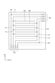
- FIG. 2 is a schematic plan view of the first substrate viewed from the Dz direction.
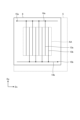
- FIG. 3 is a schematic plan view of the second substrate viewed from the Dz direction.
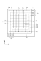
- FIG. 4 is a perspective view of a liquid crystal cell in which a first substrate and a second substrate are stacked in the Dz direction.
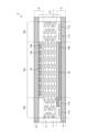
- FIG. 5 is a cross-sectional view taken along the line A-A' shown in FIG.
- FIG. 6A is a diagram showing the alignment direction of the alignment film of the first substrate.
- FIG. 6B is a diagram showing the alignment direction of the alignment film of the second substrate.
- FIG. 6A is a diagram showing the alignment direction of the alignment film of the first substrate.
- FIG. 6B is a diagram showing the alignment direction of the alignment film of the second substrate.
- FIG. 7 is a diagram of the laminated structure of the optical element according to the embodiment.
- FIG. 8A is a conceptual diagram for explaining a change in the shape of light caused by the optical element according to the embodiment.
- FIG. 8B is a conceptual diagram for explaining a change in the shape of light caused by the optical element according to the embodiment.
- FIG. 8C is a conceptual diagram for explaining a change in the shape of light caused by the optical element according to the embodiment.
- FIG. 8D is a conceptual diagram for explaining a change in the shape of light caused by the optical element according to the embodiment.
- FIG. 9 is a conceptual diagram conceptually explaining light distribution control by the lighting device according to the embodiment.
- FIG. 10 is a diagram illustrating an example of a control block configuration of the lighting device according to the first embodiment.
- FIG. 10 is a diagram illustrating an example of a control block configuration of the lighting device according to the first embodiment.
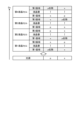
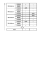
- FIG. 11 is a diagram showing an example of the correspondence between the state value of the setting circuit and each setting value.
- FIG. 12 is a flowchart illustrating an example of light distribution control processing in the lighting device according to the first embodiment.
- FIG. 13 is a sub-flowchart illustrating an example of light distribution fluctuation control processing in the lighting device according to the first embodiment.
- FIG. 14 is a sub-flowchart illustrating an example of light distribution fluctuation control processing in the lighting device according to the modification of the first embodiment.
- FIG. 15 is a diagram showing a first calculation example of intermediate gradation.
- FIG. 16 is a diagram showing a second calculation example of intermediate gradations.
- FIG. 17 is a schematic diagram showing an example of the configuration of the lighting system.
- FIG. 18 is an external view showing an example of a control device.
- FIG. 19 is a conceptual diagram showing an example of a touch detection area in a touch sensor.
- FIG. 20 is a diagram illustrating an example of a display mode of a setting change screen of the control device.
- FIG. 21 is a diagram showing an example of a control block configuration of the control device.
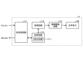
- FIG. 22 is a diagram illustrating an example of a control block configuration of the lighting device according to the second embodiment.
- FIG. 23 is a flowchart illustrating an example of light distribution control processing in the lighting system according to the second embodiment.
- FIG. 24 is a flowchart illustrating an example of a light distribution setting value change interrupt process.
- FIG. 1A is a side view showing an example of a lighting device according to an embodiment.
- FIG. 1B is a perspective view showing an example of an optical element according to an embodiment.
- the illumination device 1 includes a light source 4, a reflector 4a, and an optical element 100.
- the optical element 100 includes a first liquid crystal cell 2_1, a second liquid crystal cell 2_2, a third liquid crystal cell 2_3, and a fourth liquid crystal cell 2_4.
- the light source 4 is composed of, for example, a light emitting diode (LED).
- the reflector 4a is a component that focuses the light from the light source 4 onto the optical element 100.
- the Dz direction indicates the direction in which light is emitted from the light source 4 and the reflector 4a.
- the optical element 100 is configured by stacking a first liquid crystal cell 2_1, a second liquid crystal cell 2_2, a third liquid crystal cell 2_3, and a fourth liquid crystal cell 2_4 in the Dz direction.
- the optical element 100 is stacked in the order of a first liquid crystal cell 2_1, a second liquid crystal cell 2_2, a third liquid crystal cell 2_3, and a fourth liquid crystal cell 2_4 from the light source 4 side (lower side of FIG. 1B). It is configured.
- FIG. 1B the Dz direction indicates the direction in which light is emitted from the light source 4 and the reflector 4a.
- the optical element 100 is configured by stacking a first liquid crystal cell 2_1, a second liquid crystal cell 2_2, a third liquid crystal cell 2_3, and a fourth liquid crystal cell 2_4 in the Dz direction.
- the optical element 100 is stacked in the order of a first liquid crystal
- one direction of the plane parallel to the laminated surfaces of the first liquid crystal cell 2_1, second liquid crystal cell 2_2, third liquid crystal cell 2_3, and fourth liquid crystal cell 2_4 perpendicular to the Dz direction is the Dx direction (the first direction ), and the direction perpendicular to both the Dx direction and the Dz direction is the Dy direction (second direction).
- the first liquid crystal cell 2_1, the second liquid crystal cell 2_2, the third liquid crystal cell 2_3, and the fourth liquid crystal cell 2_4 each have a similar configuration.
- the first liquid crystal cell 2_1 and the fourth liquid crystal cell 2_4 are liquid crystal cells for p-wave polarization.
- the second liquid crystal cell 2_2 and the third liquid crystal cell 2_3 are liquid crystal cells for s-wave polarization.
- the first liquid crystal cell 2_1, the second liquid crystal cell 2_2, the third liquid crystal cell 2_3, and the fourth liquid crystal cell 2_4 are also collectively referred to as "liquid crystal cell 2.”
- the liquid crystal cell 2 includes a first substrate 5 and a second substrate 6.
- FIG. 2 is a schematic plan view of the first substrate viewed from the Dz direction.
- FIG. 3 is a schematic plan view of the second substrate viewed from the Dz direction.
- the drive electrodes are visible through the substrate, the drive electrodes and wiring are shown in solid lines for ease of understanding.
- FIG. 4 is a perspective view of a liquid crystal cell in which a first substrate and a second substrate are stacked in the Dz direction. In FIG. 4 as well, for ease of understanding, the driving electrodes and wiring on the second substrate side are shown with solid lines, and the driving electrodes and wiring on the first substrate side are shown with dotted lines.
- FIG. 4 is a perspective view of a liquid crystal cell in which a first substrate and a second substrate are stacked in the Dz direction. In FIG. 4 as well, for ease of understanding, the driving electrodes and wiring on the second substrate side are shown with solid lines, and the driving electrodes and wiring on the first substrate side are shown
- FIG. 5 is a cross-sectional view taken along the line A-A' shown in FIG. Note that in FIGS. 2, 3, 4, and 5, the drive electrodes 10a, 10b of the first substrate 5 extend in the Dx direction, and the drive electrodes 13a, 13b of the second substrate 6 extend in the Dy direction.
- a third liquid crystal cell 2_3 and a fourth liquid crystal cell 2_4 are illustrated.
- the liquid crystal cell 2 includes a liquid crystal layer 8 between a first substrate 5 and a second substrate 6, the periphery of which is sealed with a sealant 7.
- the liquid crystal layer 8 modulates the light passing through the liquid crystal layer 8 depending on the state of the electric field.
- the liquid crystal molecules positive nematic liquid crystals are used, but other liquid crystals having similar effects may also be used.
- the liquid crystal layer 8 side of the base material 9 of the first substrate 5 there are a plurality of drive electrodes 10a, 10b and a plurality of metals that supply drive voltages to be applied to these drive electrodes 10a, 10b. It includes wirings 11a and 11b, and a plurality of metal wirings 11c and 11d that supply a driving voltage to be applied to a plurality of driving electrodes 13a and 13b (see FIG. 3) provided on a second substrate 6, which will be described later.
- the metal wirings 11a, 11b, 11c, and 11d are provided in the wiring layer of the first substrate 5.
- the metal wirings 11a, 11b, 11c, and 11d are provided at intervals in the wiring layer on the first substrate 5.
- the plurality of drive electrodes 10a, 10b may be simply referred to as “drive electrodes 10.” Furthermore, the plurality of metal interconnects 11a, 11b, 11c, and 11d may be referred to as "first metal interconnects 11.” As shown in FIG. 2, in the third liquid crystal cell 2_3 and the fourth liquid crystal cell 2_4, the drive electrode 10 on the first substrate 5 extends in the Dx direction. Note that in the first liquid crystal cell 2_1 and the second liquid crystal cell 2_2, the drive electrode 10 on the first substrate 5 extends in the Dy direction.
- the plurality of drive electrodes 13a and 13b may be simply referred to as "drive electrodes 13.”
- the plurality of metal interconnects 14a and 14b may be referred to as "second metal interconnects 14.”
- the drive electrode 13 on the second substrate 6 extends in the Dy direction. Note that in the first liquid crystal cell 2_1 and the second liquid crystal cell 2_2, the drive electrode 13 on the second substrate 6 extends in the Dx direction.
- the drive electrode 10 and the drive electrode 13 are transparent electrodes formed of a transparent conductive material (transparent conductive oxide) such as ITO (Indium Tin Oxide).
- the first substrate 5 and the second substrate 6 are transparent substrates made of glass, resin, or the like.
- the first metal wiring 11 and the second metal wiring 14 are made of at least one metal material selected from aluminum (Al), copper (Cu), silver (Ag), molybdenum (Mo), or an alloy thereof. Further, the first metal wiring 11 and the second metal wiring 14 may be a laminate made of one or more of these metal materials. At least one metal material such as aluminum (Al), copper (Cu), silver (Ag), molybdenum (Mo), or an alloy thereof has a lower resistance than a transparent conductive oxide such as ITO.
- the metal wiring 11c of the first substrate 5 and the metal wiring 14a of the second substrate 6 are connected by a conductive portion 15a made of, for example, a conductive paste. Further, the metal wiring 11d of the first substrate 5 and the metal wiring 14b of the second substrate 6 are connected by a conductive portion 15b made of, for example, a conductive paste.
- connection terminal portion 16a that is connected to a flexible printed circuit (FPC) (not shown) is provided.
- FPC flexible printed circuit
- connection terminal portions 16a and 16b each include four connection terminals corresponding to the metal wirings 11a, 11b, 11c, and 11d.
- connection terminal portions 16a and 16b are provided on the wiring layer of the first substrate 5.
- a driving voltage is applied to the driving electrodes 10a, 10b on the first substrate 5 and the driving electrodes 13a, 13b on the second substrate 6 from the FPC connected to the connecting terminal part 16a or 16b. Supplied.
- the connection terminal parts 16a and 16b may be simply referred to as "the connection terminal part 16.”
- a first substrate 5 and a second substrate 6 overlap in the Dz direction (light irradiation direction), and a plurality of drive electrodes on the first substrate 5 overlap when viewed from the Dz direction. 10 and the plurality of drive electrodes 13 on the second substrate 6 intersect.
- the liquid crystal of the liquid crystal layer 8 is controlled by supplying drive voltages to the plurality of drive electrodes 10 on the first substrate 5 and the plurality of drive electrodes 13 on the second substrate 6, respectively.
- the orientation direction of the molecules 17 can be controlled.
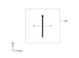
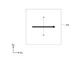
- the area in which the orientation direction of the liquid crystal molecules 17 in the liquid crystal layer 8 can be controlled is referred to as an "effective area AA.”
- an effective area AA By changing the refractive index distribution of the liquid crystal layer 8 in this effective area AA, it becomes possible to control the degree of diffusion of light transmitted through the effective area AA of the liquid crystal cell 2.
- the area where the liquid crystal layer 8 is sealed with the sealing material 7 is referred to as a "peripheral area GA" (see FIG. 5).
- the drive electrode 10 (drive electrode 10a in FIG. 5) is covered with the alignment film 18. Further, in the effective area AA of the second substrate 6, the drive electrodes 13 (drive electrodes 13a and 13b in FIG. 5) are covered by the alignment film 19.
- the orientation film 18 and the orientation film 19 have different orientation directions of liquid crystal molecules.
- FIG. 6A is a diagram showing the alignment direction of the alignment film of the first substrate.
- FIG. 6B is a diagram showing the alignment direction of the alignment film of the second substrate.
- the alignment direction of the alignment film 18 of the first substrate 5 and the alignment direction of the alignment film 19 of the second substrate 6 are directions that intersect with each other in plan view. Specifically, as shown by the solid line arrow in FIG. 6A, the alignment direction of the alignment film 18 of the first substrate 5 is perpendicular to the extending direction of the drive electrodes 10a and 10b, which is shown by the broken line arrow in FIG. 6A. Further, as shown by the solid line arrow in FIG. 6B, the alignment direction of the alignment film 19 of the second substrate 6 is perpendicular to the extending direction of the drive electrodes 13a and 13b, which is shown by the broken line arrow in FIG. 6B.
- the extending direction of each of these drive electrodes 10, 13 and the alignment direction of the alignment films 18, 19 covering it are perpendicular to each other, but these may be made at an angle other than orthogonal, for example, 85° to 90°. It does not matter if they intersect within the angular range. Further, it is preferable that the drive electrodes 10 on the first substrate 5 side and the drive electrodes 13 on the second substrate 6 side are perpendicular to each other, but they may also intersect at an angle of 85° to 90°, for example. do not have.
- the alignment direction of the alignment films 18 and 19 is formed by a rubbing process or a photo alignment process.
- FIG. 7 is a diagram of the laminated structure of the optical element according to the embodiment.
- 8A, FIG. 8B, FIG. 8C, and FIG. 8D are conceptual diagrams for explaining changes in the shape of light caused by the optical element according to the embodiment. 8A, FIG. 8B, FIG. 8C, and FIG. 8D show examples in which a potential difference is generated between each drive electrode of the shaded substrate of each liquid crystal cell 2.
- the optical element 100 is provided on the optical axis of the light source 4 shown by the dashed line, and as described above, from the light source 4 side (lower side in FIG. 7), the first liquid crystal cell 2_1, the first liquid crystal cell 2_1, the A second liquid crystal cell 2_2, a third liquid crystal cell 2_3, and a fourth liquid crystal cell 2_4 are stacked in this order.
- the third liquid crystal cell 2_3 and the fourth liquid crystal cell 2_4 are stacked while being rotated by 90 degrees with respect to the first liquid crystal cell 2_1 and the second liquid crystal cell 2_2.
- the alignment direction of the alignment film intersects on the first substrate 5 side and the second substrate 6 side, as shown in FIGS. 6A and 6B.
- the direction of the liquid crystal molecules in the liquid crystal layer 8 gradually changes from the Dx direction to the Dy direction (or from the Dy direction to the Dx direction) as it goes from the first substrate 5 side to the second substrate 6 side.
- the polarization component of the transmitted light rotates along the axis.
- the polarized light component that was a p-polarized light component on the first substrate 5 side changes to an s-polarized light component as it moves toward the second substrate 6, and the polarized light that was an s-polarized light component on the first substrate 5 side changes to an s-polarized light component as it moves toward the second substrate 6 side.
- the component changes to a p-polarized component as it moves toward the second substrate 6 side.
- Such rotation of polarized light components may be referred to as optical rotation.
- FIG. 8A shows a state in which no potential is generated between adjacent electrodes of each liquid crystal cell 2. In this case, only optical rotation occurs in each liquid crystal cell 2, and none of the polarized light components is diffused.
- the liquid crystal molecules are aligned in an arc shape between the electrodes, and this Accordingly, a refractive index distribution is formed in the liquid crystal layer 8 along the Dx direction.
- the refractive index distribution acts on the polarized light component parallel to the Dx direction (the p polarized light component in FIG. 8B), thereby causing the p polarized light component to be diffused in the Dx direction. do.
- the s-polarized light component is diffused in the Dy direction. That is, the polarized light component that changed from the p-polarized light component to the s-polarized light component while passing through the liquid crystal layer 8 of the first liquid crystal cell 2_1 will now be diffused in the Dy direction as well.
- the s-polarized light component when it enters the first liquid crystal cell 2_1 undergoes optical rotation while passing through the liquid crystal layer 8, but since it becomes a polarized light component that intersects with any refractive index distribution, it is only rotated without being diffused. It passes through the first liquid crystal cell 2_1.
- the degree of light diffusion in each direction depends on the potential difference between adjacent drive electrodes 10a and 10b (or between drive electrodes 13a and 13b). If the potential difference between the drive electrodes 10a and 10b (or between the drive electrodes 13a and 13b) is a predefined maximum potential difference (for example, 30 [V]), the spread of light in that direction will be the maximum (100 [%]). , if no potential difference is generated at all, no light spreads in that direction (0 [%]). Alternatively, if the potential difference between the drive electrodes 10a and 10b (or between the drive electrodes 13a and 13b) is 50% (for example, 15V) of the maximum potential difference, the spread of light in that direction is 50%. becomes. Note that if the relationship between the voltage difference and the spread of light is not linear, it is possible to set the voltage difference to another potential difference instead of 15 [V].
- each liquid crystal cell 2 has a wide gap (also referred to as a cell gap) between the substrates (between the first substrate 5 and the second substrate 6), which is approximately 30 ⁇ m to 50 ⁇ m.
- the effect of the electric field formed on one substrate on the other substrate is suppressed as much as possible.
- the drive voltage that generates the potential difference between the adjacent drive electrodes 10a and 10b (or between the drive electrodes 13a and 13b) is a so-called AC square wave, and it goes without saying that this prevents the burn-in of liquid crystal molecules. .
- each alignment film the extending direction of the drive electrode of each substrate, and the angle formed between these may be determined depending on the characteristics of the liquid crystal employed and the optical characteristics desired to be applied to the entire optical element 100 or the liquid crystal cell 2. It can be changed as appropriate.
- a configuration in which four first liquid crystal cells 2_1, a second liquid crystal cell 2_2, a third liquid crystal cell 2_3, and a fourth liquid crystal cell 2_4 are stacked is described for the optical element 100;
- a configuration in which two or three liquid crystal cells 2 are stacked, or a configuration in which five or more liquid crystal cells 2 are stacked can also be adopted.
- the illumination device 1 having the above-described configuration, by controlling the drive voltage of each liquid crystal cell 2, light incident on the optical element from the light source 4 is directed in the Dx direction (horizontal diffusion direction) and the Dy direction (vertical diffusion direction). control in two directions (direction).
- the above-mentioned vertical diffusion and horizontal diffusion may be collectively referred to as light diffusion.
- the shape of the light is the shape of light appearing on a plane parallel to the output surface of the optical element, and may also be referred to as a light distribution shape.
- control of the degree of light diffusion in the present disclosure will be described with reference to FIG. 9.
- FIG. 9 is a conceptual diagram conceptually explaining control of light diffusion degree by the lighting device according to the embodiment.
- FIG. 9 shows the irradiation range of light on the virtual plane xy perpendicular to the Dz direction. Note that the outline of the actual irradiation range becomes somewhat unclear due to the distance to the light source 4, light diffraction phenomenon, and the like.
- the light distribution shape in the Dx direction changes depending on the drive voltage applied to the drive electrode 10 or the drive electrode 13 extending in the Dy direction in each liquid crystal cell 2.
- Such diffusion of light in the Dx direction may be referred to as lateral diffusion.
- the light distribution shape in the Dy direction changes depending on the drive voltage applied to the drive electrode 10 or the drive electrode 13 extending in the Dx direction in the first to fourth liquid crystal cells.
- Such diffusion of light in the Dy direction may be referred to as vertical diffusion.
- the minimum diffusivity of horizontal diffusion and vertical diffusion is 0 [%], and the maximum diffusivity is 100 [%]. More specifically, when the lateral diffusivity is 0%, a drive electrode that functions to widen the light distribution state in the Dx direction (for example, a drive electrode that extends in the Dy direction on the first substrate 5 of the first liquid crystal cell 2_1) The drive electrode 10) does not affect the refractive index distribution of the liquid crystal layer 8. In this case, there is either no potential difference between the adjacent drive electrodes 10a and 10b, or no potential is supplied to the electrodes.
- the drive electrode that functions to widen the light distribution state in the Dx direction (for example, the drive electrode 10 extending in the Dy direction on the first substrate 5 of the first liquid crystal cell 2_1) has the greatest effect on the refractive index distribution of the liquid crystal layer 8.
- the potential difference between the adjacent drive electrodes 10a and 10b is set to the maximum potential difference (for example, 30 [V]) in the optical element 100.
- the potential difference between the adjacent drive electrodes 10a and 10b is greater than 0 [V] and smaller than the maximum potential difference (for example, 30 [V]).
- a potential adjusted to is applied to the electrode. The same applies to vertical diffusion.
- a contour a shown in FIG. 9 exemplifies the irradiation range when both the horizontal diffusivity and the vertical diffusivity are 100%.
- a contour b shown in FIG. 9 illustrates an irradiation range when the horizontal diffusivity is 100 [%] and the vertical diffusivity is 0 [%].
- a contour c shown in FIG. 9 exemplifies the irradiation range when the horizontal diffusivity is 0 [%] and the vertical diffusivity is 100 [%].
- the contour d shown in FIG. 9 illustrates the irradiation range when both the horizontal diffusivity and the vertical diffusivity are 0 [%]. That is, the contour d shows the light distribution state when the light from the light source 4 is emitted without being controlled in any way by the optical element 100 (so to speak, it passes through the optical element 100 as it is).
- the horizontal and vertical diffusivity of the light emitted from the optical element 100 can be controlled.
- the light distribution shape of the emitted light from the lighting device 1 can be changed.
- the control for changing the light distribution shape of the light emitted from the lighting device 1 will also be referred to as "light distribution control.”
- a lighting device 1 that can control light distribution in two directions, the Dx direction and the Dy direction, is exemplified, but parameters that can be controlled in the lighting device 1 are not limited to light distribution (spread of light).
- the lighting device 1 may have a mode in which dimming control is possible.
- the controllable parameters in the lighting device 1 may include dimming (brightness).
- the following describes the configuration and operation of a lighting device 1 capable of controlling light distribution in two directions, the Dx direction and the Dy direction, that can dynamically control the light distribution state in the two directions, the Dx direction and the Dy direction, using 1/f fluctuation. explain.
- dynamic light distribution control using 1/f fluctuation may be simply referred to as “fluctuation control.”
- dynamic light distribution control using 1/f fluctuation in the present disclosure refers to control in which the magnitude of fluctuation (light distribution shape) changes with time.
- dynamic light distribution control using 1/f fluctuation in the present disclosure refers to control in which the light distribution shape changes over time due to 1/f fluctuation.
- the Dx direction is assumed to be the H direction (first direction)
- the Dy direction is assumed to be the V direction (second direction).
- FIG. 10 is a diagram illustrating an example of a control block configuration of the lighting device according to the first embodiment.
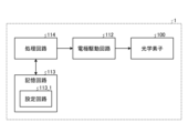
- the illumination device 1 according to the embodiment includes an electrode drive circuit 112, a memory circuit 113, and a processing circuit 114 as control blocks for controlling the optical element 100 described above.
- the processing circuit 114 is composed of a microcomputer for executing light distribution control and dimming control of the lighting device 1.
- the electrode drive circuit 112 supplies a drive voltage to each drive electrode 10 and 13 of each liquid crystal cell 2 of the optical element 100 based on the processing result in the processing circuit 114. Processing in the processing circuit 114 will be described later.
- the storage circuit 113 includes, for example, an internal memory installed in a microcomputer that constitutes the processing circuit 114.
- the storage area of the storage circuit 113 stores a light distribution set value S0h in the H direction and a light distribution set value S0v in the V direction of the lighting device 1.
- the direction of lateral diffusion is assumed to be the H direction
- the degree of diffusion in the lateral direction is assumed to be the light distribution setting value in the H direction
- the direction of vertical diffusion is taken as the V direction
- the degree of diffusion in the vertical direction (vertical diffusivity) is taken as the light distribution setting value in the V direction.
- the H-direction light distribution setting value S0h and the V-direction light distribution setting value S0v stored in the storage area of the storage circuit 113 are, for example, settings stored in the storage area of the storage circuit 113 when the lighting device 1 was operated last time. It may be a value, or it may be transmitted from a control device (not shown) and stored in a storage area of the storage circuit 113.
- intermediate data of processing in the processing circuit 114 is temporarily stored in the storage area of the storage circuit 113.
- the storage circuit 113 includes a setting circuit 113_1 for setting various setting items such as enabling or disabling the fluctuation control and a fluctuation width that defines the range of change in the light distribution value due to the fluctuation control.
- the setting circuit 113_1 is exemplified by, for example, a DIP switch (Dual In-line Package switch) that can set each setting item.
- the setting circuit 113_1 is exemplified to have a configuration including a plurality of two-state switch circuits of "0" and "1", for example.
- FIG. 11 is a diagram showing an example of the correspondence between the state value of the setting circuit and each set value.
- the setting circuit 113_1 includes four switch circuits, and is configured such that the upper two bits enable or disable the fluctuation control, and the lower two bits set the fluctuation width.
- the setting value items include enabling or disabling of fluctuation control of dimming (brightness) (dimming fluctuation control), and fluctuation width.
- the dimming fluctuation width when the dimming fluctuation control is enabled (the upper two bits are "01") is "00" in the lower two bits of the state value of the setting circuit 113_1. It is set as “5 [%]”. Further, when the lower two bits of the state value of the setting circuit 113_1 are "01”, it is set as “10 [%]”. Further, when the lower two bits of the state value of the setting circuit 113_1 are "10”, it is set as "20 [%]”. Further, when the lower two bits of the state value of the setting circuit 113_1 are "11”, it is set as "30 [%]".
- the light distribution fluctuation width when the light distribution fluctuation control is enabled (the upper two bits are “10") is "00" in the lower two bits of the state value of the setting circuit 113_1. It is set as “5 [%]”. Further, when the lower two bits of the state value of the setting circuit 113_1 are "01”, it is set as “10 [%]”. Further, when the lower two bits of the state value of the setting circuit 113_1 are "10”, it is set as "20 [%]”. Further, when the lower two bits of the state value of the setting circuit 113_1 are "11”, it is set as "30 [%]".
- the dimming fluctuation width and the light distribution fluctuation width when both the dimming fluctuation control and the light distribution fluctuation control are valid are determined by the setting circuit 113_1.
- the lower two bits of the state value are "00”, it is set as "5 [%]”.
- the lower two bits of the state value of the setting circuit 113_1 are "01”, it is set as "10 [%]”.
- the lower two bits of the state value of the setting circuit 113_1 are "10
- the lower two bits of the state value of the setting circuit 113_1 are "11”, it is set as "30 [%]”.
- the number of switches in the setting circuit 113_1 is not limited to the above. Specifically, for example, by setting the number of switches for setting the fluctuation width to three or more, the number of fluctuation width options can be increased. Furthermore, for example, the light distribution fluctuation width in the H direction and the light distribution fluctuation width in the V direction in the light distribution fluctuation control may be set to different values. In this case, for example, the total value of the light distribution fluctuation width in the H direction and the light distribution fluctuation width in the V direction in the light distribution fluctuation control may be a predetermined value (for example, 100 [%]), Furthermore, in the light distribution fluctuation control, only one of the light distribution fluctuation width in the H direction and the light distribution fluctuation width in the V direction may be set.
- the following description will describe light distribution fluctuation control, and will omit description of dimming fluctuation control.
- the number of switches in the setting circuit 113_1 for setting whether fluctuation control is enabled or disabled is set to 1, and "0" disables fluctuation control, and "1" disables fluctuation control. It's okay.
- each setting item such as enabling or disabling the fluctuation control and fluctuation width in the fluctuation control may be, for example, a setting value stored in the storage area of the storage circuit 113 when the lighting device 1 was operated last time.
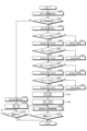
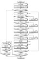
- FIG. 12 is a flowchart illustrating an example of light distribution control processing in the lighting device according to the first embodiment.
- the processing circuit 114 reads a state value from the setting circuit 113_1 of the storage circuit 113 (step S101), and determines whether fluctuation control is effective based on the state value (step S101). Step S102). Specifically, the processing circuit 114 reads the state value of the setting circuit 113_1, and determines that the fluctuation control is effective when the upper two bits of the state value are "10". Further, the processing circuit 114 determines that the fluctuation control is invalid when the upper two bits of the state value are "00".
- a description of the case where the upper two bits of the state value are "01" or "11” will be omitted.
- step S102 If the fluctuation control is invalid (step S102; No), specifically, if the upper two bits of the setting circuit 113_1 are "00", the processing circuit 114 controls the H direction stored in the storage area of the storage circuit 113.
- the light distribution setting value S0h and the light distribution setting value S0v in the V direction are read out (step S103), and the light distribution setting value S0h and the light distribution setting value S0v expressed as a percentage from 0 [%] to 100 [%] are These are converted into light distribution gradation values Dh and Dv of the optical element 100, respectively (step S104), and output to the electrode drive circuit 112.
- the light distribution gradation value Dh in the H direction is expressed by the following equation (1).
- the light distribution gradation value Dv in the V direction is expressed by the following equation (2).
- the light distribution gradation of the optical element 100 is, for example, "255".
- the light distribution gradation values Dh and Dv are 8-bit data.
- the light distribution gradation of the optical element 100 is not limited to "255". In other words, the light distribution gradation values Dh and Dv are not limited to 8-bit data.
- the present disclosure is not limited by the light distribution gradation of the optical element 100.
- the electrode drive circuit 112 supplies drive voltages corresponding to the light distribution gradation values Dh and Dv output from the processing circuit 114 to each drive electrode 10 and 13 of each liquid crystal cell 2 of the optical element 100. Thereby, the light distribution state is controlled according to the light distribution set value S0h in the H direction and the light distribution set value S0v in the V direction.
- the processing circuit 114 determines whether the power of the lighting device 1 is controlled to be turned off (step S105), and if the power of the lighting device 1 is not controlled to be turned off (step S105; No), repeats the process of step S105. When this is executed and the power of the lighting device 1 is controlled to be turned off (step S105; Yes), the light distribution control process ends.
- step S102 When the fluctuation control is valid (step S102; Yes), specifically, when the upper two bits of the setting circuit 113_1 are "10", the processing circuit 114 controls the H direction stored in the storage area of the storage circuit 113.
- the light distribution setting value S0h in the V direction and the light distribution setting value S0v in the V direction are read (step S106), and a fluctuation range defined as a change range of the light distribution value in the light distribution fluctuation control process to be described later is set.
- the H-direction light distribution setting value S0h and the V-direction light distribution setting value S0v stored in the storage area of the storage circuit 113 will also be referred to as "initial setting values.”
- the processing circuit 114 sets the fluctuation width ⁇ to 5% and sets the lower and upper limits of the fluctuation range of the light distribution value. do.
- the processing circuit 114 sets the fluctuation width ⁇ to 10% and sets the lower and upper limits of the fluctuation range of the light distribution value.
- the processing circuit 114 sets the fluctuation width ⁇ to 20% and sets the lower and upper limits of the fluctuation range of the light distribution value.
- the processing circuit 114 sets the fluctuation width ⁇ to 30% and sets the lower and upper limits of the fluctuation range of the light distribution value.
- the upper limit value Shmax of the fluctuation range of the light distribution value Sh with respect to the light distribution set value S0h in the H direction is set (steps S011 to S013).
- the processing circuit 114 determines whether the value obtained by adding the fluctuation width ⁇ to the light distribution setting value S0h in the H direction is less than or equal to 100% (step S011). If the value obtained by adding the fluctuation width ⁇ to the light distribution set value S0h is less than or equal to 100% (step S011; Yes), the processing circuit 114 determines the upper limit of the fluctuation range of the light distribution value Sh with respect to the light distribution set value S0h. Shmax is set to S0h+ ⁇ [%] (step S012) and stored in the storage area of the storage circuit 113.
- step S011 If the value obtained by adding the fluctuation width ⁇ to the light distribution set value S0h exceeds 100 [%] (step S011; No), the processing circuit 114 determines the upper limit of the fluctuation range of the light distribution value Sh with respect to the light distribution set value S0h.
- the value Shmax is set to 100[%] (step S013) and stored in the storage area of the storage circuit 113.
- the lower limit value Shmin of the fluctuation range of the light distribution value Sh with respect to the light distribution set value S0h in the H direction is set (steps S021 to S023).
- the processing circuit 114 determines whether the value obtained by subtracting the fluctuation width ⁇ from the light distribution setting value S0h in the H direction is 0 [%] or more (step S021). If the value obtained by subtracting the fluctuation width ⁇ from the light distribution set value S0h is 0 [%] or more (step S021; Yes), the processing circuit 114 determines the lower limit of the fluctuation range of the light distribution value Sh with respect to the light distribution set value S0h. Shmin is set to S0h- ⁇ [%] (step S022) and stored in the storage area of the storage circuit 113.
- step S021 If the value obtained by subtracting the fluctuation width ⁇ from the light distribution set value S0h is less than 0 [%] (step S021; No), the processing circuit 114 determines the lower limit of the fluctuation range of the light distribution value Sh with respect to the light distribution set value S0h.
- the value Shmin is set to 0 [%] (step S023) and stored in the storage area of the storage circuit 113.
- the upper limit value Svmax of the fluctuation range of the light distribution value Sv with respect to the light distribution set value S0v in the V direction is set (steps S031 to S033).
- the processing circuit 114 determines whether the value obtained by adding the fluctuation width ⁇ to the light distribution setting value S0v in the V direction is less than or equal to 100% (step S031). If the value obtained by adding the fluctuation width ⁇ to the light distribution set value S0v is 100% or less (step S031; Yes), the processing circuit 114 determines the upper limit of the fluctuation range of the light distribution value Sv with respect to the light distribution set value S0v. Svmax is set to S0v+ ⁇ [%] (step S032) and stored in the storage area of the storage circuit 113.
- step S031 If the value obtained by adding the fluctuation width ⁇ to the light distribution set value S0v exceeds 100 [%] (step S031; No), the processing circuit 114 determines the upper limit of the fluctuation range of the light distribution value Sv with respect to the light distribution set value S0v.
- the value Svmax is set to 100 [%] (step S033) and is stored in the storage area of the storage circuit 113.
- the lower limit value Svmin of the fluctuation range of the light distribution value Sv with respect to the light distribution set value S0v in the V direction is set (steps S041 to S043).
- the processing circuit 114 determines whether the value obtained by subtracting the fluctuation width ⁇ from the light distribution setting value S0v in the V direction is 0 [%] or more (step S041). If the value obtained by subtracting the fluctuation width ⁇ from the light distribution set value S0v is 0 [%] or more (step S041; Yes), the processing circuit 114 determines the lower limit of the fluctuation range of the light distribution value Sv with respect to the light distribution set value S0v. Svmin is set to S0v- ⁇ [%] (step S042) and stored in the storage area of the storage circuit 113.
- step S041 If the value obtained by subtracting the fluctuation width ⁇ from the light distribution set value S0v is less than 0 [%] (step S041; No), the processing circuit 114 determines the lower limit of the fluctuation range of the light distribution value Sv with respect to the light distribution set value S0v.
- the value Svmin is set to 0 [%] (step S043) and stored in the storage area of the storage circuit 113.
- Setting process of the upper limit value Shmax of the fluctuation range of the light distribution value Sh (steps S011 to S013), setting process of the lower limit value Shmin of the fluctuation range of the light distribution value Sh (steps S021 to S023), fluctuation of the light distribution value Sv
- the execution order of the process for setting the upper limit value Svmax of the range (steps S031 to S033) and the process for setting the lower limit value Svmin of the fluctuation range of the light distribution value Sv (steps S041 to S043) is not limited to the above. Alternatively, each of these setting processes may be processed in parallel.
- the processing circuit 114 generates a first light distribution value Sh in the H direction expressed as a percentage from 0 [%] to 100 [%] as pre-processing for executing the light distribution fluctuation control process (step S200) to be described later.
- (t) and the first light distribution value Sv(t) in the V direction are converted into light distribution gradation values Dh(t) and Dv(t) in the optical element 100, respectively, and output to the electrode drive circuit 112 ( Step S108).
- the light distribution gradation value Dh(t) in the H direction is expressed by the following equation (3).
- the light distribution gradation value Dv(t) in the V direction is expressed by the following equation (4).
- the electrode drive circuit 112 supplies drive voltages according to the light distribution gradation values Dh(t) and Dv(t) output from the processing circuit 114 to each drive electrode 10 and 13 of each liquid crystal cell 2 of the optical element 100. do.
- the light distribution state is controlled in accordance with the initial setting values (H-direction light distribution setting value S0h and V-direction light distribution setting value S0v) stored in the storage area of the storage circuit 113.
- FIG. 13 is a sub-flowchart illustrating an example of light distribution fluctuation control processing in the lighting device according to the first embodiment.
- the sub-flowchart shown in FIG. 13 corresponds to the light distribution fluctuation control process (step S200) in the light distribution control process shown in FIG.
- an intermittent chaos method is used as an algorithm for realizing dynamic light distribution control using 1/f fluctuation.
- the variable X(t+1) at time t+1 is represented by the variable X(t) at time t (0.0 ⁇ X(t) ⁇ 1.0). More specifically, the variable X(t+1) at time t+1 is expressed by the following equation (5) when 0.0 ⁇ X(t) ⁇ 0.5, and 0.5 ⁇ X(t) In the case of ⁇ 1.0, it is expressed by the following formula (6).
- the variable X(t+1) is a target value at time t+1 after time t.
- the execution interval of the light distribution fluctuation control process (that is, the time from time t to time t+1) is, for example, 100 [ms]. The present disclosure is not limited by the execution interval of the light distribution fluctuation control process.
- the execution interval of the light distribution fluctuation control process (step S200) is controlled by the timer value tf. That is, the time-up value TF of the timer value tf corresponds to the execution interval of the light distribution fluctuation control process.
- the timer value tf is reset at the start of the light distribution fluctuation control process.
- a second light distribution value Sh(t+1) which is a target light distribution value in the H direction at time t+1.
- the first light distribution value Sh(t) in the H direction at time t is defined by the following equation (7), where the variable X(t) at time t in the intermittent chaos method is the first variable Xh(t) in the H direction. .
- the processing circuit 114 reads out the upper limit value Shmax and lower limit value Shmin of the fluctuation range of the light distribution value Sh stored in the storage area of the storage circuit 113 (step S201), and calculates the following equation (8), which is a modification of the above equation (7). is used to calculate the first variable Xh(t) at time t (step S202). It is assumed that the following equation (8) is stored in a storage area of the storage circuit 113, for example.
- the processing circuit 114 calculates the second variable Xh(t+1) in the H direction at time t+1. Specifically, the processing circuit 114 determines whether the first variable Xh(t) in the H direction calculated in step S202 is less than 0.5 (step S203), and determines whether Xh(t) ⁇ 0.5. If so (step S203; Yes), the second variable Xh(t+1) in the H direction at time t+1 is calculated using the following equation (9), which is a modification of the above equation (5) (step S204). If Xh(t) ⁇ 0.5 (step S203; No), calculate the second variable Xh(t+1) in the H direction at time t+1 using the following equation (10), which is a modification of the above equation (6). (Step S205). It is assumed that the following equations (9) and (10) are stored in a storage area of the storage circuit 113, for example.
- the processing circuit 114 determines whether the second variable Xh(t+1) in the H direction calculated in step S204 or step S205 is greater than or equal to 0.01 and less than or equal to 0.99 (step S206). If 0.01 ⁇ Xh(t+1) ⁇ 0.99 (step S206; Yes), the process advances to step S208.
- the second variable Xh(t+1) in the H direction is less than 0.01 (0 ⁇ Xh(t+1) ⁇ 0.01) or greater than 0.99 (0.99 ⁇ Xh(t+1) ⁇ 1 .0) (step S206; No)
- the processing circuit 114 sets the second variable Xh(t+1) in the H direction to a random value within the range of 0.01 or more and 0.99 or less (step S207), The process advances to step S208.
- the processing circuit 114 sets the second variable Xh (t+1) in the H direction to a random value between 0.01 and 0.99 using, for example, a random number table stored in the storage area of the storage circuit 113. do.
- the processing in steps S206 and S207 can prevent the second variable Xh(t+1) in the H direction from sticking to 0.0 or 1.0.
- the processing circuit 114 applies the second variable Xh(t+1) in the H direction obtained by the processing from step S203 to step S207 to the following equation (11), which is a modification of the above equation (7), to calculate H at time t+1.
- a second light distribution value Sh (t+1) which is a target light distribution value in the direction, is calculated and stored in the storage area of the storage circuit 113 (step S208). It is assumed that the following equation (11) is stored in a storage area of the storage circuit 113, for example.
- a second light distribution value Sv(t+1) which is a target light distribution value in the V direction at time t+1.
- the first light distribution value Sv(t) in the V direction at time t is expressed by the following equation (12), where the variable X(t) at time t in the intermittent chaos method is the first variable Xv(t) in the V direction. .
- the processing circuit 114 reads out the upper limit value Svmax and lower limit value Svmin of the fluctuation range of the light distribution value Sv stored in the storage area of the storage circuit 113 (step S211), and calculates the following equation (13), which is a modification of the above equation (12). is used to calculate the first variable Xv(t) at time t (step S212). It is assumed that the following equation (13) is stored in a storage area of the storage circuit 113, for example.
- the processing circuit 114 calculates the second variable Xv(t+1) at time t+1. Specifically, the processing circuit 114 determines whether the first variable Xv(t) in the V direction calculated in step S212 is less than 0.5 (step S213), and determines whether Xv(t) ⁇ 0.5. If so (step S213; Yes), the second variable Xv(t+1) in the V direction at time t+1 is calculated using the following equation (14), which is a modification of the above equation (5) (step S214). If Xv(t) ⁇ 0.5 (step S213; No), calculate the second variable Xv(t+1) in the V direction at time t+1 using the following equation (15), which is a modification of the above equation (6). (Step S215). It is assumed that the following equations (14) and (15) are stored in a storage area of the storage circuit 113, for example.
- the processing circuit 114 determines whether the second variable Xv(t+1) in the V direction calculated in step S214 or step S215 is greater than or equal to 0.01 and less than or equal to 0.99 (step S216). If 0.01 ⁇ Xv(t+1) ⁇ 0.99 (step S216; Yes), the process advances to step S218.
- the second variable Xv(t+1) in the V direction is less than 0.01 (0 ⁇ Xv(t+1) ⁇ 0.01) or greater than 0.99 (0.99 ⁇ Xv(t+1) ⁇ 1 .0) (step S216; No), the processing circuit 114 sets the second variable Xv(t+1) in the V direction to a random value within the range of 0.01 or more and 0.99 or less (step S217), The process advances to step S218. At this time, the processing circuit 114 sets the second variable Xv(t+1) in the V direction to a random value of 0.01 to 0.99 using, for example, a random number table stored in the storage area of the storage circuit 113. do.
- the processing in steps S216 and S217 can prevent the second variable Xv(t+1) in the V direction from sticking to 0.0 or 1.0.
- the processing circuit 114 applies the second variable Xv(t+1) obtained by the processing from step S213 to step S217 to the following equation (16), which is a modification of the above equation (12), to calculate the arrangement in the V direction at time t+1.
- the second light distribution value Sv(t+1) which is the light target value, is calculated and stored in the storage area of the storage circuit 113 (step S218). It is assumed that the following equation (16) is stored in a storage area of the storage circuit 113, for example.
- the processing circuit 114 respectively calculates the first light distribution value Sh (t+1) in the H direction and the first light distribution value Sv (t+1) in the V direction, which are expressed in percentages from 0 [%] to 100 [%]. , converted into light distribution gradation values Dh(t+1) and Dv(t+1) in the optical element 100 (step S221), and output to the electrode drive circuit 112.
- the light distribution gradation value Dh(t+1) in the H direction is expressed by the following equation (17).
- the light distribution gradation value Dv(t+1) in the V direction is expressed by the following equation (18).
- the electrode drive circuit 112 supplies drive voltages according to the light distribution gradation values Dh(t+1) and Dv(t+1) output from the processing circuit 114 to each drive electrode 10 and 13 of each liquid crystal cell 2 of the optical element 100. do. As a result, the light distribution state is controlled according to the first light distribution value Sh(t+1) in the H direction and the first light distribution value Sv(t+1) in the V direction.
- the processing circuit 114 updates the second light distribution value Sh(t+1), which is the light distribution target value in the H direction at time t+1, as a new first light distribution value Sh(t) in the H direction at time t.
- the processing circuit 114 determines whether or not the power of the lighting device 1 has been controlled to turn off (step S109), and if the power of the lighting device 1 has not been controlled to turn off (step S109; No), the process returns to step S200 and the process shown in FIG.
- the light distribution fluctuation control process shown in 13 is repeatedly executed, and when the power of the lighting device 1 is controlled to be turned off (step S109; Yes), the light distribution control process is ended.
- the light distribution state of the optical element 100 is dynamically controlled. As a result, the light distribution shape of the lighting device 1 changes as if it were wavering, making it possible to produce comfortable light.
- FIG. 14 is a sub-flowchart illustrating an example of light distribution fluctuation control processing in the lighting device according to the modification of the first embodiment.
- the sub-flowchart shown in FIG. 14 corresponds to the light distribution fluctuation control process (step S200) in the light distribution control process shown in FIG. Note that here, points different from the subflowchart shown in FIG. 13 will be explained in detail, and redundant explanation will be omitted.
- the light distribution gradation value at time t is the light distribution target value at time t+1 (steps S201 to S218) .
- the light distribution gradation value at time t is the light distribution gradation value at time t and Light distribution control is performed in stages at intermediate gradations from the light distribution gradation value at time t+1.
- a specific process of executing light distribution control at a light distribution control interval shorter than the execution interval of the light distribution fluctuation control process will be described.
- the count value n is expressed as an integer from 1 to the number of divisions N.
- the count-up interval (that is, the light distribution control interval at intermediate gradations) is 20 [ms]. Note that the present disclosure is not limited by the number of divisions of the execution interval of the light distribution fluctuation control process or the light distribution control interval at intermediate gradations. Alternatively, for example, it is also possible to transmit the division number N input by the user from a control device (not shown) and store it in the storage circuit 113.
- the count-up timer value ts that measures the time from count value n to n+1 reaches the time-up value TS
- the processing circuit 114 calculates the light distribution value Sh (t+n/N) in the H direction and the light distribution value Sv (t+n/N) in the V direction at each time (t+n/N) divided into N (step S232).
- the light distribution value Sh (t+n/N) in the H direction at each time (t+n/N) is expressed by the following equation (19).
- the light distribution value Sv (t+n/N) in the V direction at each time (t+n/N) is expressed by the following equation (20).
- the processing circuit 114 calculates the light distribution value Sh (t+n/N) and the light distribution value Sv (t+n/N) expressed in percentages from 0 [%] to 100 [%], respectively, in the optical element 100. It is converted into optical gradation values Dh (t+n/N) and Dv (t+n/N) (step S233), and output to the electrode drive circuit 112.
- the light distribution gradation value Dh(t+n/N) in the H direction is expressed by the following equation (21).
- the light distribution gradation value Dv(t+n/N) in the V direction is expressed by the following equation (22).
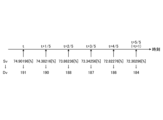
- FIG. 15 is a diagram showing a first calculation example of intermediate gradations.
- the light distribution value in the H direction is Sh
- the light distribution gradation value is Dh.
- the first light distribution value Sh(t) in the H direction at time t is 25.09804[%]
- the light distribution gradation value Dh(t) is 64.000002 ( ⁇ 64)
- the first light distribution value Sh(t) in the H direction at time t+1 is 25.09804[%].
- the second light distribution value Sh (t+1) which is the light target value
- the light distribution gradation value Dh (t+1) is 70.627452 ( ⁇ 71)
- the light distribution value Sh(t+n/N) in the H direction at each time (t+n/N) is converted to the following light distribution gradation value Dh(t+n/N) using the above equation (21). Note that the light distribution gradation value Dh(t+n/N) in the H direction is a value rounded to the nearest whole number.
- FIG. 16 is a diagram showing a second example of intermediate gradation calculation.
- the light distribution value in the V direction is Sv
- the light distribution gradation value is Dv.
- the first light distribution value Sv(t) in the V direction at time t is 74.90196[%]
- the light distribution gradation value Dv(t) is 190.999998 ( ⁇ 191)
- the first light distribution value Sv(t) in the V direction at time t+1 is 74.90196[%].
- the second light distribution value Sv (t+1) which is the light target value
- the light distribution gradation value Dh (t+1) is 184.372548 ( ⁇ 184)
- the light distribution value Sv(t+n/N) in the V direction at each time (t+n/N) is converted to the following light distribution gradation value Dv(t+n/N) using the above equation (22).
- the light distribution gradation value Dv(t+n/N) in the V direction is a value rounded to the nearest whole number.
- the processing circuit 114 calculates the second light distribution value Sh(t+1), which is the light distribution target value in the H direction at time t+1, at time t+1.
- the process returns to the light distribution control process shown in 12.
- the light distribution value Sh (t+n/N) in the H direction and the light distribution value Sv (t+n/N) in the V direction are set.
- the light distribution state is controlled according to the
- the first light distribution value Sh(t) in the H direction at time t is , and the second light distribution value Sh(t+1), which is the light distribution target value in the H direction at time t+1, can be smoothed.
- the first light distribution value Sv(t) in the V direction at time t and the second light distribution value Sv(t) which is the light distribution target value in the V direction at time t+1 are obtained. Changes in the light distribution state between the light value Sv(t+1) and the light value Sv(t+1) can be made smooth. Thereby, changes in fluctuations in the light distribution shape of the lighting device 1 can be smoothed.
- the lighting device 1 has a configuration that allows light distribution control in two directions, the H direction and the V direction, and dynamic control due to 1/f fluctuation in the H direction and the V direction, respectively.
- Execute light distribution control Thereby, for example, more natural and comfortable light can be produced than when dynamic control using 1/f fluctuation is applied to dimming control (brightness control).
- the light distribution gradation value at time t and the light distribution gradation value at time t+1 are set at a light distribution control interval shorter than the execution interval of the light distribution fluctuation control process. Light distribution is controlled in stages at intermediate gradations. Thereby, changes in the light distribution state can be made smooth.
- FIG. 17 is a schematic diagram showing an example of the configuration of the lighting system.
- the lighting system includes lighting devices 1 (1_1, 1_2, . . . , 1_N) and a control device 200.
- the control device 200 is exemplified by a portable communication terminal device such as a smartphone or a tablet.
- the lighting devices 1 (1_1, 1_2, . . . , 1_N) are registered in advance in the control device 200 as control target devices whose light distribution can be controlled by the control device 200.
- the communication means 300 is, for example, a wireless communication means such as Bluetooth (registered trademark) or WiFi (registered trademark).
- the lighting device 1 (1_1, 1_2, . . . , 1_N) and the control device 200 may perform wireless communication via a predetermined network such as a mobile communication network, for example.
- the lighting device 1 (1_1, 1_2, . . . , 1_N) and the control device 200 may be connected by wire to perform wire communication.
- FIG. 17 shows an example in which a plurality of lighting devices 1 (1_1, 1_2, ..., 1_N) are registered, in the present disclosure, at least one control target device capable of controlling light distribution is registered. It is sufficient that the lighting device 1 is registered.
- the control device 200 is configured to be able to change the light distribution state of the lighting device 1 in the H direction and the V direction.
- each setting item such as enabling or disabling the fluctuation control and the fluctuation width, is set by a setting circuit 113_1 (for example, a DIP switch) provided in the lighting device 1.
- a setting circuit 113_1 for example, a DIP switch
- FIG. 18 is an external view showing an example of a control device.
- the control device 200 is a display device with a touch detection function (touch screen) in which a display panel 20 and a touch sensor 30 are integrated.
- the control device 200 includes internal components such as various ICs such as a detection IC and a display IC, a CPU (Central Processing Unit), a RAM (Random Access Memory), and an EEPROM of a smartphone or tablet that constitutes the control device 200. (Electrically Erasable Programmable Read Only Memory), ROM (Read Only Memory), GPU (Graphics Processing Unit), etc.
- the display panel 20 is a so-called in-cell type or hybrid type device that has a touch sensor 30 built-in and integrated. Integrating the touch sensor 30 into the display panel 20 means, for example, that some members such as the substrate and electrodes used as the display panel 20 and some parts such as the substrate and electrodes used as the touch sensor 30. This includes using the same member as the other member. Note that the display panel 20 may be a so-called on-cell type device in which a touch sensor 30 is mounted on a display device.
- the display panel 20 is a liquid crystal display panel using a liquid crystal display element.
- the display panel 20 is not limited to this, and may be, for example, an organic EL display panel (OLED: Organic Light Emitting Diode) or an inorganic EL display panel (micro LED, mini LED).
- OLED Organic Light Emitting Diode
- micro LED mini LED
- the touch sensor 30 is a capacitive touch sensor.
- the touch sensor 30 is not limited to this, and may be, for example, a resistive film type touch sensor, an ultrasonic type touch sensor, or an optical type touch sensor.
- FIG. 19 is a conceptual diagram showing an example of a touch detection area in a touch sensor.
- a plurality of detection elements 31 are provided in the detection area FA of the touch sensor 30.
- the plurality of detection elements 31 are arranged in a matrix in the detection area FA of the touch sensor 30 in the X direction and the Y direction perpendicular to the X direction.
- the touch sensor 30 has a detection area FA that overlaps a plurality of detection elements 31 arranged in the X direction and the Y direction.
- FIG. 20 is a diagram illustrating an example of the display mode of the setting change screen of the control device.
- the display panel 20 is provided with a display area DA that overlaps the detection area FA of the touch sensor 30 in plan view, and a setting change screen shown in FIG. 20 is displayed in the display area DA.
- an HV plane is defined whose origin is O(0,0) at a predetermined position on the setting change screen shown in FIG.
- a light distribution shape object OBJ whose center point is the origin O(0,0) of the HV plane on the setting change screen is displayed, and the illumination shape object OBJ is displayed on the outline of this light distribution shape object OBJ.
- a first slider S1 for changing the light distribution state of the device 1 in the H direction and a second slider S2 for changing the light distribution state of the lighting device 1 in the V direction are arranged.
- the light distribution shape object OBJ is an image corresponding to the light distribution state of light emitted from the lighting device 1.
- the first slider S1 and the second slider S2 are, for example, images displayed on the display area DA, and can be moved (drag operation) by touching with a user's finger.
- the shape of the light distribution shape object OBJ can be changed. At the same time, the light distribution state of the lighting device 1 in the H direction is controlled. Further, by moving the second slider S2 in the V direction, the shape of the light distribution shape object OBJ can be changed. At the same time, the light distribution state of the lighting device 1 in the V direction is controlled.
- the shape of the light distribution shape object OBJ on the setting change screen is circular or elliptical depending on the light distribution value Sh in the H direction and the light distribution value Sv in the V direction.
- the shape of the light distribution shape object OBJ changes to a circle or an ellipse as the first slider S1 and second slider S2 move.
- the first slider S1 is set from the position on the outline of the light distribution shape object OBJ when the light distribution value Sh in the H direction is 0 [%] to the position on the outline of the light distribution shape object OBJ when the light distribution value Sh in the H direction is 100 [%]. Movement in the H direction is possible up to a position on the outline of the light distribution shape object OBJ.
- the second slider S2 is set from the position on the outline of the light distribution shape object OBJ when the light distribution value Sv in the V direction is 0 [%] to the position on the outline of the light distribution shape object OBJ when the light distribution value Sv in the V direction is 100 [%]. Movement in the V direction is possible up to a position on the outline of the light distribution shape object OBJ.
- the light distribution value Sh in the H direction of the lighting device 1 is set by the amount of movement of the position h of the intersection of the H axis of the HV plane and the outline of the light distribution shape object OBJ. Can be done.
- the position h of the intersection of the H-axis and the outline of the light distribution shape object OBJ is set as the center point of the first slider S1.
- the position h0 of the first slider S1 on the display area DA overlaps with the position h of the intersection of the H-axis and the outline of the light distribution shape object OBJ.
- the light distribution value Sh of the lighting device 1 in the H direction can be changed.
- “Sh” in FIG. 20 indicates the light distribution value (for example, “50” [%]) of the lighting device 1 in the H direction.
- the light distribution value Sv in the V direction of the lighting device 1 is set by the amount of movement of the position v of the intersection of the V axis of the HV plane and the outline of the light distribution shape object OBJ. can do.
- the position v of the intersection of the V-axis and the outline of the light distribution shape object OBJ is set as the center point of the second slider S2.
- the position v0 of the second slider S2 on the display area DA overlaps with the position v of the intersection of the V-axis and the outline of the light distribution shape object OBJ.
- FIG. 21 is a diagram showing an example of the control block configuration of the control device.
- a control block configuration for changing the light distribution state of the lighting device 1 in the H direction and the V direction will be described.
- the control device 200 includes a display panel 20, a touch sensor 30, a detection circuit 211, a conversion processing circuit 212, a storage circuit 223, a transmission/reception circuit 225, and a display control circuit 231.
- the detection circuit 211 is composed of, for example, a detection IC.
- the detection circuit 211 and the display control circuit 231 may be mounted on the display panel 20 as one display IC, or may be mounted on an FPC connected to the display panel 20.
- the conversion processing circuit 212 and the storage circuit 223 are configured by, for example, a CPU, RAM, EEPROM, ROM, etc. of a smartphone or tablet that constitutes the control device 200.
- the display control circuit 231 may be a display IC mounted on the display panel 20 as described above, or may include a GPU of a smartphone, tablet, etc. that constitutes the control device 200. Also good.
- the transmitting/receiving circuit 225 is configured with a wireless communication module such as a smartphone or a tablet that configures the control device 200, for example.
- the detection circuit 211 is a circuit that detects the presence or absence of a touch on the touch sensor 30 based on the detection signal output from each detection element 31 of the touch sensor 30.
- the conversion processing circuit 212 is a circuit that performs conversion processing between the touch detection position in the detection circuit 211 and various setting values (light distribution values in this disclosure) of the lighting device 1.
- the conversion processing circuit 212 has a function of performing conversion processing between the touch detection position in the detection circuit 211, the position of the touched object (image), and the operation state on various screens. ing.
- the conversion processing circuit 212 is a component implemented by, for example, a CPU of a smartphone, tablet, or the like that constitutes the control device 200.
- the storage circuit 223 is composed of, for example, a RAM, an EEPROM, a ROM, etc. of a smartphone or tablet that constitutes the control device 200. In the present disclosure, the storage circuit 223 stores various setting values (in the present disclosure, light distribution values) of the lighting device 1.
- the transmitting/receiving circuit 225 transmits and receives various setting values (light distribution values in this disclosure) to and from the lighting device 1. Specifically, the transmitting/receiving circuit 225 transmits the H-direction light distribution value Sh and the V-direction light distribution value Sv set by the control device 200 to the lighting device 1 as light distribution set values S1h and S1v, respectively. Further, the transmitting/receiving circuit 225 receives the light distribution setting values S0h and S0v transmitted from the lighting device 1.
- the display control circuit 231 executes display control processing to display the above-mentioned setting change screen on the display panel 20.
- the display control circuit 231 controls the display of the display panel 20 based on various setting values (in this disclosure, light distribution values) and position information of the image stored in the storage circuit 223.
- FIG. 22 is a diagram illustrating an example of a control block configuration of the lighting device according to the second embodiment.
- the same components as those in the control block configuration of the illumination device 1 according to Embodiment 1 are given the same reference numerals, and redundant explanations may be omitted.
- the lighting device 1a according to the second embodiment includes a transmitting/receiving circuit 111 in addition to the configuration of the lighting device 1 according to the first embodiment described above.
- the transmitting/receiving circuit 111 transmits and receives various setting values (light distribution setting values in this disclosure) to and from the control device 200. Specifically, the transmitting/receiving circuit 111 receives the light distribution setting values S1h and S1v transmitted from the control device 200. Further, the transmitting/receiving circuit 111 transmits the light distribution setting values S0h and S0v stored in the storage area of the storage circuit 113 to the control device 200.
- the transmitting/receiving circuit 111 transmits the light distribution setting values S0h and S0v stored in the storage area of the memory circuit 113 to the control device 200 when the lighting device 1 is started, and the light distribution transmitted from the control device 200.
- the set values S1h and S1v are stored in the storage area of the storage circuit 113 as new light distribution set values S0h and S0v. That is, by transmitting the light distribution setting values S1h, S1v from the control device 200 to the lighting device 1a, the light distribution setting values S0h, S0v in the storage area of the storage circuit 113 are updated to the light distribution setting values S1h, S1v. be done.
- the lighting device 1 does not store the light distribution set values S0h and S0v for the first time (both the light distribution set values S0h and S0v are 0 [%]). In this case, by transmitting the light distribution setting values S1h, S1v from the control device 200, the light distribution setting values S0h, S0v are stored in the storage area of the storage circuit 113.
- the present invention is not limited to the above, and a configuration may be adopted in which predetermined values such as 50% are stored as the initial light distribution setting values S0h and S0v.
- FIG. 23 is a flowchart illustrating an example of light distribution control processing in the lighting system according to the second embodiment. Note that here, points different from Embodiment 1 will be explained in detail, and duplicate explanation will be omitted.
- the processing circuit 114 reads out the H-direction light distribution setting value S0h and the V-direction light distribution setting value S0v stored in the storage area of the storage circuit 113, and the control device 200 (step S301).
- the transmitting/receiving circuit 225 of the control device 200 stores the light distribution setting values S0h and S0v transmitted from the lighting device 1a in the storage circuit 223.
- the display control circuit 231 of the control device 200 reads out the light distribution setting values S0h, S0v stored in the storage circuit 223, and changes the settings according to the light distribution setting values S0h, S0v.
- the display control of the display panel 20 is performed so that the shape of the light distribution shape object OBJ, the position of the first slider S1, the Dx direction light distribution display, the position of the second slider S2, and the Dy direction light distribution display are reflected on the setting change screen. Execute. Thereby, the control device 200 shifts to a standby state for a change operation.
- the processing circuit 114 of the lighting device 1a reads the state value from the setting circuit 113_1 of the storage circuit 113 (step S302), and determines whether fluctuation control is effective based on the state value (step S303).
- step S303; No If the fluctuation control is invalid (step S303; No), the processing circuit 114 reads out the H-direction light distribution setting value S0h and the V-direction light distribution setting value S0v stored in the storage area of the storage circuit 113 (step S303; No). S304), the light distribution setting value S0h and the light distribution setting value S0v expressed in percentages from 0 [%] to 100 [%] are converted into light distribution gradation values Dh and Dv of the optical element 100, respectively (step S305), output to the electrode drive circuit 112.
- the electrode drive circuit 112 supplies drive voltages corresponding to the light distribution gradation values Dh and Dv output from the processing circuit 114 to each drive electrode 10 and 13 of each liquid crystal cell 2 of the optical element 100. Thereby, the light distribution state is controlled according to the light distribution set value S0h in the H direction and the light distribution set value S0v in the V direction.
- the processing circuit 114 determines whether the H-direction light distribution setting value S0h and the V-direction light distribution setting value S0v stored in the storage area of the storage circuit 113 have not been changed (step S306). .
- FIG. 24 is a flowchart illustrating an example of a light distribution setting value change interrupt process.
- step S307 if the H-direction light distribution setting value S0h and the V-direction light distribution setting value S0v stored in the storage area of the storage circuit 113 have not been changed (S306; Yes), the processing circuit 114 It is determined whether the power of the lighting device 1a is controlled to be turned off (step S307), and if the power of the lighting device 1a is not controlled to be turned off (step S307; No), the processes from step S306 to step S307 are repeatedly executed.
- step S304 If the H-direction light distribution setting value S0h and the V-direction light distribution setting value S0v stored in the storage area of the storage circuit 113 have been changed (S306; No), the processes from step S304 to step S306 are repeatedly executed. . As a result, the light distribution state is controlled according to the changed light distribution set value S0h in the H direction and light distribution set value S0v in the V direction.
- step S307 When the power of the lighting device 1a is controlled to be turned off (step S307; Yes), the light distribution control process ends.
- step S303; Yes If the fluctuation control is valid (step S303; Yes), the processing circuit 114 reads out the H-direction light distribution setting value S0h and the V-direction light distribution setting value S0v stored in the storage area of the storage circuit 113 (step S303; Yes). 308), setting the fluctuation range of the light distribution value in the light distribution fluctuation control process.
- the processing circuit 114 sets the light distribution set value S0h in the H direction as the first light distribution value Sh(t) at time t, and sets the light distribution set value S0v in the V direction as the first light distribution value Sh(t) at time t.
- the processing circuit 114 After outputting the light distribution gradation values Dh(t) and Dv(t) to the electrode drive circuit 112 (step S310), the processing circuit 114 performs the light distribution fluctuation control process shown in FIG. 13 or 14 (step S200). Execute.
- the processing circuit 114 determines whether the H-direction light distribution setting value S0h and the V-direction light distribution setting value S0v stored in the storage area of the storage circuit 113 have not been changed (step S311). .
- step S311 If the H-direction light distribution setting value S0h and the V-direction light distribution setting value S0v stored in the storage area of the storage circuit 113 have not been changed (step S311; Yes), the processing circuit 114 changes the power supply of the lighting device 1a. It is determined whether the lighting device 1a is controlled to be turned off (step S312), and if the power of the lighting device 1a is not controlled to be turned off (step S312; No), the process returns to step S200 and the light distribution fluctuation control shown in FIG. 13 or 14 is performed. Repeat the process.
- step S311 If the H-direction light distribution setting value S0h and the V-direction light distribution setting value S0v stored in the storage area of the storage circuit 113 have been changed (step S311; No), the processes from step S308 onwards are repeatedly executed. As a result, the light distribution fluctuation control shown in FIG. 13 or 14 is executed based on the changed light distribution set value S0h in the H direction and light distribution set value S0v in the V direction, and the light distribution state of the optical element 100 is changed. controlled.
- step S312 When the power of the lighting device 1a is controlled to be turned off (step S312; Yes), the light distribution control process ends.
- the lighting device 1a of the lighting system uses the light distribution setting values S1h, S1v transmitted from the control device 200 as new light distribution setting values S0h, S0v in the storage circuit 113 by the interrupt process shown in FIG.
- the information is stored in the storage area (step S402), and the processing from step S304 to step S307 or the processing from step S308 to step S312 is executed.
- the control device 200 can change the light distribution setting values S0h, S0v of the lighting device 1a, and when the fluctuation control is disabled (step S303; No), the lighting When the light distribution setting values S0h, S0v of the device 1a are changed (step S306; No), normal light distribution control is executed based on the changed light distribution setting values S0h, S0v, and fluctuation control is effective. (Step S303; Yes), when the light distribution setting values S0h, S0v of the lighting device 1a are changed (Step S311; No), the light distribution setting values S0h, S0v are changed based on the changed light distribution setting values S0h, S0v. Perform dynamic light distribution control.
- the light distribution state of the optical element 100 is dynamically controlled by repeatedly executing the light distribution fluctuation control process shown in FIG. 13.
- the light distribution shape of the lighting device 1 changes as if it were wavering, making it possible to produce comfortable light.
- each time (t+n/N) from time t to time t+1 is , the light distribution is controlled at an intermediate gradation between the H-direction light distribution gradation value Dh(t) at time t and the H-direction light distribution gradation value Dh(t+1) at time t+1. Also, at each time (t+n/N) from time t to time t+1, the light distribution gradation value Dv(t) in the V direction at time t, and the light distribution gradation value Dv(t+1) in the V direction at time t+1. Light distribution is controlled at intermediate gradations.
- the mode in which the light distribution state in two directions, the H direction (first direction) and the V direction (second direction), is independently and dynamically controlled was exemplified.
- the present invention is not limited to the mode in which the light distribution state in the two directions of the H direction (first direction) and the V direction (second direction) is independently and dynamically controlled.
- a mode may also be adopted in which at least one light distribution state is dynamically controlled.
Landscapes
- Engineering & Computer Science (AREA)
- Physics & Mathematics (AREA)
- Chemical & Material Sciences (AREA)
- Crystallography & Structural Chemistry (AREA)
- Computer Hardware Design (AREA)
- General Physics & Mathematics (AREA)
- Theoretical Computer Science (AREA)
- Spectroscopy & Molecular Physics (AREA)
- General Engineering & Computer Science (AREA)
- Liquid Crystal (AREA)
Abstract
Description
図10は、実施形態1に係る照明装置の制御ブロック構成の一例を示す図である。図10に示すように、実施形態に係る照明装置1は、上述した光学素子100を制御するための制御ブロックとして、電極駆動回路112、記憶回路113、及び処理回路114を備える。処理回路114は、照明装置1の配光制御や調光制御を実行するためのマイコンで構成される。
図14は、実施形態1の変形例に係る照明装置における配光ゆらぎ制御処理の一例を示すサブフローチャートである。図14に示すサブフローチャートは、図12に示す配光制御処理における配光ゆらぎ制御処理(ステップS200)に対応する。なお、ここでは、図13に示すサブフローチャートとは異なる点について詳細に説明し、重複する説明は省略する。
=Sh(t)+[(Sh(t+1)-Sh(t))/N]×n・・・(19)
=Sv(t)+[(Sv(t+1)-Sv(t))/N]×n・・・(20)
=Sh(t+n/N)×階調/100・・・(21)
=Sv(t+n/N)×階調/100・・・(22)
Sh(t+2/5)=26.13764[%]
Sh(t+3/5)=26.65744[%]
Sh(t+4/5)=27.17724[%]
Sh(t+5/5)=Sh(t+1)=27.69704[%]
Dh(t+2/5)=66.650982≒67
Dh(t+3/5)=67.976472≒68
Dh(t+4/5)=69.301962≒69
Dh(t+5/5)=Dh(t+1)=70.627452≒71
Sv(t+2/5)=73.86236[%]
Sv(t+3/5)=73.34256[%]
Sv(t+4/5)=72.82276[%]
Sv(t+5/5)=Sv(t+1)=72.30296[%]
Dv(t+2/5)=188.349018≒188
Dv(t+3/5)=187.023528≒187
Dv(t+4/5)=185.698038≒186
Dv(t+5/5)=Dv(t+1)=184.372548≒184
図17は、照明システムの構成の一例を示す概略図である。照明システムは、照明装置1(1_1,1_2,・・・,1_N)と、制御装置200と、を含む。制御装置200は、例えば、スマートフォンやタブレット等の携帯可能な通信端末装置が例示される。照明装置1(1_1,1_2,・・・,1_N)は、制御装置200によって配光制御可能な制御対象デバイスとして、制御装置200に予め登録されている。
2 液晶セル
2_1 第1液晶セル
2_2 第2液晶セル
2_3 第3液晶セル
2_4 第4液晶セル
4 光源
5 第1基板
6 第2基板
7 封止材
8 液晶層
9 基材
10,10a,10b 駆動電極
11 第1金属配線
11a,11b,11c,11d 金属配線
12 基材
13,13a,13b 駆動電極
14 第2金属配線
14a,14b 金属配線
15a,15b 導通部
16a,16b 接続端子部
17 液晶分子
18 配向膜
19 配向膜
20 表示パネル
30 タッチセンサ
31 検出素子
100 光学素子
111 送受信回路
112 電極駆動回路
113 記憶回路
113_1 設定回路(DIPスイッチ)
200 制御装置
211 検出回路
212 変換処理回路
223 記憶回路
225 送受信回路
231 表示制御回路
300 通信手段
AA 有効領域
DA 表示領域
FA 検出領域
GA 周辺領域
OBJ 配光形状オブジェクト
S1 第1スライダ
S2 第2スライダ
Sh 配光値(H方向)
Sh(t) 第1配光値(H方向)
Sh(t+1) 第2配光値(H方向)
Sv 配光値(V方向)
Sv(t) 第1配光値(V方向)
Sv(t+1) 第2配光値(V方向)
Xh(t) 第1変数(H方向)
Xh(t+1) 第2変数(H方向)
Xv(t) 第1変数(V方向)
Xv(t+1) 第2変数(V方向)
Claims (15)
- 光源と、
前記光源の光軸上に設けられ、当該光源から射出される光の配光状態を第1方向と当該第1方向とは異なる第2方向の2方向で制御する光学素子と、
少なくとも前記光学素子の配光制御処理を実行する処理回路と、
を備え、
前記処理回路は、
前記配光制御処理を実行するための設定値である配光設定値に基づき、前記第1方向及び前記第2方向の少なくとも一方の配光状態を1/fゆらぎにより動的に制御する、
照明装置。 - 前記処理回路は、
前記第1方向及び前記第2方向の2方向の配光状態をそれぞれ独立して動的に制御する、
請求項1に記載の照明装置。 - 前記処理回路は、
間欠カオス法を用いて、1/fゆらぎによる動的な配光制御を行う、
請求項1又は2に記載の照明装置。 - 前記動的な配光制御を実行する際の配光値の変化幅を定義するゆらぎ幅が設定される記憶回路を備え、
前記処理回路は、
前記動的な配光制御を実行する際に、当該制御における配光値の変化範囲として定義されるゆらぎ範囲を設定し、
前記配光設定値と前記ゆらぎ幅とを加算して、前記ゆらぎ範囲の上限値とし、前記配光設定値から前記ゆらぎ幅を減算して、前記ゆらぎ範囲の下限値とする、
請求項3に記載の照明装置。 - 前記処理回路は、
前記動的な配光制御を実行する際に、時刻tにおいて前記光学素子の配光状態を実現するための配光値である第1配光値、及び、前記ゆらぎ範囲の上下限値に基づいて、前記時刻tにおける第1変数を算出し、当該第1変数に基づき、前記時刻tよりも後の時刻t+1における第2変数を算出し、当該第2変数、及び、前記ゆらぎ範囲の上下限値に基づいて、前記時刻t+1における前記光学素子の配光状態を実現するための配光目標値である第2配光値を算出する、
請求項4に記載の照明装置。 - 前記処理回路は、
前記第2変数が所定範囲外であるとき、当該所定範囲内のランダム値を第2変数として前記第2配光値を算出する、
請求項5に記載の照明装置。 - 前記処理回路は、
前記動的な配光制御を実行する際に、前記時刻tにおける前記第1配光値と、前記時刻t+1における前記第2配光値との中間階調で、前記時刻tから前記時刻t+1までの間に段階的に前記光学素子の配光状態を変化させる、
請求項6に記載の照明装置。 - 光源と、該光源の光軸上に設けられ、当該光源から射出される光の配光状態を第1方向と当該第1方向とは異なる第2方向の2方向で制御する光学素子と、少なくとも前記光学素子の配光制御処理を実行する処理回路と、を備えた照明装置と、
少なくとも前記照明装置の前記第1方向及び前記第2方向の2方向の配光状態を変更可能な制御装置と、
を備え、
前記処理回路は、
前記配光制御処理を実行するための設定値である配光設定値に基づき、前記第1方向及び前記第2方向の少なくとも一方の配光状態を1/fゆらぎにより動的に制御する、
照明システム。 - 前記処理回路は、
前記第1方向及び前記第2方向の2方向の配光状態をそれぞれ独立して動的に制御する、
請求項8に記載の照明システム。 - 前記処理回路は、
間欠カオス法を用いて、1/fゆらぎによる動的な配光制御を行う、
請求項8又は9に記載の照明システム。 - 前記照明装置は、
前記動的な配光制御を実行する際の配光値の変化幅を定義するゆらぎ幅が設定される記憶回路を備え、
前記処理回路は、
前記動的な配光制御を実行する際に、当該制御における配光値の変化範囲として定義されるゆらぎ範囲を設定し、
前記配光設定値と前記ゆらぎ幅とを加算して、前記ゆらぎ範囲の上限値とし、前記配光設定値から前記ゆらぎ幅を減算して、前記ゆらぎ範囲の下限値とする、
請求項10に記載の照明システム。 - 前記処理回路は、
前記動的な配光制御を実行する際に、時刻tにおいて前記光学素子の配光状態を実現するための配光値である第1配光値、及び、前記ゆらぎ範囲の上下限値に基づいて、前記時刻tにおける第1変数を算出し、当該第1変数に基づき、前記時刻tよりも後の時刻t+1における第2変数を算出し、当該第2変数、及び、前記ゆらぎ範囲の上下限値に基づいて、前記時刻t+1における前記光学素子の配光状態を実現するための配光目標値である第2配光値を算出する、
請求項11に記載の照明システム。 - 前記処理回路は、
前記第2変数が所定範囲外であるとき、当該所定範囲内のランダム値を第2変数として前記第2配光値を算出する、
請求項12に記載の照明システム。 - 前記処理回路は、
前記動的な配光制御を実行する際に、前記時刻tにおける前記第1配光値と、前記時刻t+1における前記第2配光値との中間階調で、前記時刻tから前記時刻t+1までの間に段階的に前記光学素子の配光状態を変化させる、
請求項13に記載の照明システム。 - 前記制御装置は、
前記配光設定値を前記照明装置に送信し、
前記照明装置は、
前記制御装置から送信された配光設定値を前記記憶回路の記憶領域に格納する、
請求項11に記載の照明システム。
Priority Applications (3)
| Application Number | Priority Date | Filing Date | Title |
|---|---|---|---|
| JP2024536905A JP7735573B2 (ja) | 2022-07-27 | 2023-07-05 | 照明装置、及び照明システム |
| CN202380056247.2A CN119605317A (zh) | 2022-07-27 | 2023-07-05 | 照明装置以及照明系统 |
| US19/034,921 US12482435B2 (en) | 2022-07-27 | 2025-01-23 | Illumination device and illumination system |
Applications Claiming Priority (2)
| Application Number | Priority Date | Filing Date | Title |
|---|---|---|---|
| JP2022-119986 | 2022-07-27 | ||
| JP2022119986 | 2022-07-27 |
Related Child Applications (1)
| Application Number | Title | Priority Date | Filing Date |
|---|---|---|---|
| US19/034,921 Continuation US12482435B2 (en) | 2022-07-27 | 2025-01-23 | Illumination device and illumination system |
Publications (1)
| Publication Number | Publication Date |
|---|---|
| WO2024024433A1 true WO2024024433A1 (ja) | 2024-02-01 |
Family
ID=89706155
Family Applications (1)
| Application Number | Title | Priority Date | Filing Date |
|---|---|---|---|
| PCT/JP2023/024995 Ceased WO2024024433A1 (ja) | 2022-07-27 | 2023-07-05 | 照明装置、及び照明システム |
Country Status (4)
| Country | Link |
|---|---|
| US (1) | US12482435B2 (ja) |
| JP (1) | JP7735573B2 (ja) |
| CN (1) | CN119605317A (ja) |
| WO (1) | WO2024024433A1 (ja) |
Citations (2)
| Publication number | Priority date | Publication date | Assignee | Title |
|---|---|---|---|---|
| JP2021077609A (ja) * | 2019-11-10 | 2021-05-20 | こもれびエンジニアリング合同会社 | 照明装置 |
| JP2021096957A (ja) * | 2019-12-17 | 2021-06-24 | 三菱電機株式会社 | 照明システムおよび照明装置 |
Family Cites Families (2)
| Publication number | Priority date | Publication date | Assignee | Title |
|---|---|---|---|---|
| JPH0265001A (ja) | 1988-08-30 | 1990-03-05 | Sekisui Chem Co Ltd | 照明器具の調光装置 |
| JP5006120B2 (ja) | 2007-06-25 | 2012-08-22 | パナソニック株式会社 | 照明制御装置 |
-
2023
- 2023-07-05 JP JP2024536905A patent/JP7735573B2/ja active Active
- 2023-07-05 WO PCT/JP2023/024995 patent/WO2024024433A1/ja not_active Ceased
- 2023-07-05 CN CN202380056247.2A patent/CN119605317A/zh active Pending
-
2025
- 2025-01-23 US US19/034,921 patent/US12482435B2/en active Active
Patent Citations (2)
| Publication number | Priority date | Publication date | Assignee | Title |
|---|---|---|---|---|
| JP2021077609A (ja) * | 2019-11-10 | 2021-05-20 | こもれびエンジニアリング合同会社 | 照明装置 |
| JP2021096957A (ja) * | 2019-12-17 | 2021-06-24 | 三菱電機株式会社 | 照明システムおよび照明装置 |
Also Published As
| Publication number | Publication date |
|---|---|
| CN119605317A (zh) | 2025-03-11 |
| JPWO2024024433A1 (ja) | 2024-02-01 |
| JP7735573B2 (ja) | 2025-09-08 |
| US20250166581A1 (en) | 2025-05-22 |
| US12482435B2 (en) | 2025-11-25 |
Similar Documents
| Publication | Publication Date | Title |
|---|---|---|
| WO2019024596A1 (zh) | 调光器件及其制作方法、背光源组件以及显示装置 | |
| WO2023145347A1 (ja) | 照明装置及び照明制御システム | |
| JP2025525120A (ja) | 表示パネル及び表示装置 | |
| JP7746591B2 (ja) | 照明システム及び制御装置 | |
| WO2024024433A1 (ja) | 照明装置、及び照明システム | |
| JP7570541B2 (ja) | 照明装置 | |
| WO2024185300A1 (ja) | 照明システム | |
| JP7763386B2 (ja) | 照明装置の制御装置 | |
| JP7592898B2 (ja) | 照明システム | |
| JP7708975B2 (ja) | 照明装置の制御装置、及び照明システム | |
| JP7735595B2 (ja) | 照明装置の制御装置 | |
| JP7615362B2 (ja) | 照明システムの制御装置 | |
| TW202242512A (zh) | 電子裝置及顯示投影系統 | |
| JP7542756B2 (ja) | 照明装置の制御装置 | |
| WO2024135247A1 (ja) | 照明装置の制御装置 | |
| US20260004750A1 (en) | Control device for illumination device | |
| HK40118948A (zh) | 照明系统以及控制装置 | |
| JP2021113884A (ja) | 調光フィルムおよび調光デバイス | |
| TWI863746B (zh) | 調節裝置 | |
| HK40116976A (zh) | 照明装置的控制装置以及照明系统 | |
| JP6575156B2 (ja) | 照明装置 |
Legal Events
| Date | Code | Title | Description |
|---|---|---|---|
| 121 | Ep: the epo has been informed by wipo that ep was designated in this application |
Ref document number: 23846166 Country of ref document: EP Kind code of ref document: A1 |
|
| WWE | Wipo information: entry into national phase |
Ref document number: 2024536905 Country of ref document: JP |
|
| WWE | Wipo information: entry into national phase |
Ref document number: 202380056247.2 Country of ref document: CN |
|
| NENP | Non-entry into the national phase |
Ref country code: DE |
|
| WWP | Wipo information: published in national office |
Ref document number: 202380056247.2 Country of ref document: CN |
|
| 122 | Ep: pct application non-entry in european phase |
Ref document number: 23846166 Country of ref document: EP Kind code of ref document: A1 |