WO2024023969A1 - 検査用パターンおよびそれを備えた半導体集積回路 - Google Patents
検査用パターンおよびそれを備えた半導体集積回路 Download PDFInfo
- Publication number
- WO2024023969A1 WO2024023969A1 PCT/JP2022/028926 JP2022028926W WO2024023969A1 WO 2024023969 A1 WO2024023969 A1 WO 2024023969A1 JP 2022028926 W JP2022028926 W JP 2022028926W WO 2024023969 A1 WO2024023969 A1 WO 2024023969A1
- Authority
- WO
- WIPO (PCT)
- Prior art keywords
- pad
- semiconductor integrated
- pillar
- inspection
- optical
- Prior art date
- Legal status (The legal status is an assumption and is not a legal conclusion. Google has not performed a legal analysis and makes no representation as to the accuracy of the status listed.)
- Ceased
Links
Images





Classifications
-
- H—ELECTRICITY
- H10—SEMICONDUCTOR DEVICES; ELECTRIC SOLID-STATE DEVICES NOT OTHERWISE PROVIDED FOR
- H10P—GENERIC PROCESSES OR APPARATUS FOR THE MANUFACTURE OR TREATMENT OF DEVICES COVERED BY CLASS H10
- H10P74/00—Testing or measuring during manufacture or treatment of wafers, substrates or devices
- H10P74/27—Structural arrangements therefor
- H10P74/273—Interconnections for measuring or testing, e.g. probe pads
-
- G—PHYSICS
- G01—MEASURING; TESTING
- G01R—MEASURING ELECTRIC VARIABLES; MEASURING MAGNETIC VARIABLES
- G01R31/00—Arrangements for testing electric properties; Arrangements for locating electric faults; Arrangements for electrical testing characterised by what is being tested not provided for elsewhere
- G01R31/28—Testing of electronic circuits, e.g. by signal tracer
- G01R31/2851—Testing of integrated circuits [IC]
- G01R31/2884—Testing of integrated circuits [IC] using dedicated test connectors, test elements or test circuits on the IC under test
-
- H—ELECTRICITY
- H10—SEMICONDUCTOR DEVICES; ELECTRIC SOLID-STATE DEVICES NOT OTHERWISE PROVIDED FOR
- H10W—GENERIC PACKAGES, INTERCONNECTIONS, CONNECTORS OR OTHER CONSTRUCTIONAL DETAILS OF DEVICES COVERED BY CLASS H10
- H10W72/00—Interconnections or connectors in packages
- H10W72/071—Connecting or disconnecting
-
- G—PHYSICS
- G02—OPTICS
- G02F—OPTICAL DEVICES OR ARRANGEMENTS FOR THE CONTROL OF LIGHT BY MODIFICATION OF THE OPTICAL PROPERTIES OF THE MEDIA OF THE ELEMENTS INVOLVED THEREIN; NON-LINEAR OPTICS; FREQUENCY-CHANGING OF LIGHT; OPTICAL LOGIC ELEMENTS; OPTICAL ANALOGUE/DIGITAL CONVERTERS
- G02F1/00—Devices or arrangements for the control of the intensity, colour, phase, polarisation or direction of light arriving from an independent light source, e.g. switching, gating or modulating; Non-linear optics
- G02F1/01—Devices or arrangements for the control of the intensity, colour, phase, polarisation or direction of light arriving from an independent light source, e.g. switching, gating or modulating; Non-linear optics for the control of the intensity, phase, polarisation or colour
- G02F1/21—Devices or arrangements for the control of the intensity, colour, phase, polarisation or direction of light arriving from an independent light source, e.g. switching, gating or modulating; Non-linear optics for the control of the intensity, phase, polarisation or colour by interference
- G02F1/212—Mach-Zehnder type
-
- G—PHYSICS
- G02—OPTICS
- G02F—OPTICAL DEVICES OR ARRANGEMENTS FOR THE CONTROL OF LIGHT BY MODIFICATION OF THE OPTICAL PROPERTIES OF THE MEDIA OF THE ELEMENTS INVOLVED THEREIN; NON-LINEAR OPTICS; FREQUENCY-CHANGING OF LIGHT; OPTICAL LOGIC ELEMENTS; OPTICAL ANALOGUE/DIGITAL CONVERTERS
- G02F1/00—Devices or arrangements for the control of the intensity, colour, phase, polarisation or direction of light arriving from an independent light source, e.g. switching, gating or modulating; Non-linear optics
- G02F1/01—Devices or arrangements for the control of the intensity, colour, phase, polarisation or direction of light arriving from an independent light source, e.g. switching, gating or modulating; Non-linear optics for the control of the intensity, phase, polarisation or colour
- G02F1/21—Devices or arrangements for the control of the intensity, colour, phase, polarisation or direction of light arriving from an independent light source, e.g. switching, gating or modulating; Non-linear optics for the control of the intensity, phase, polarisation or colour by interference
- G02F1/225—Devices or arrangements for the control of the intensity, colour, phase, polarisation or direction of light arriving from an independent light source, e.g. switching, gating or modulating; Non-linear optics for the control of the intensity, phase, polarisation or colour by interference in an optical waveguide structure
-
- H—ELECTRICITY
- H10—SEMICONDUCTOR DEVICES; ELECTRIC SOLID-STATE DEVICES NOT OTHERWISE PROVIDED FOR
- H10W—GENERIC PACKAGES, INTERCONNECTIONS, CONNECTORS OR OTHER CONSTRUCTIONAL DETAILS OF DEVICES COVERED BY CLASS H10
- H10W72/00—Interconnections or connectors in packages
- H10W72/20—Bump connectors, e.g. solder bumps or copper pillars; Dummy bumps; Thermal bumps
- H10W72/251—Materials
- H10W72/252—Materials comprising solid metals or solid metalloids, e.g. PbSn, Ag or Cu
-
- H—ELECTRICITY
- H10—SEMICONDUCTOR DEVICES; ELECTRIC SOLID-STATE DEVICES NOT OTHERWISE PROVIDED FOR
- H10W—GENERIC PACKAGES, INTERCONNECTIONS, CONNECTORS OR OTHER CONSTRUCTIONAL DETAILS OF DEVICES COVERED BY CLASS H10
- H10W72/00—Interconnections or connectors in packages
- H10W72/90—Bond pads, in general
- H10W72/951—Materials of bond pads
- H10W72/952—Materials of bond pads comprising metals or metalloids, e.g. PbSn, Ag or Cu
Definitions
- the present disclosure relates to a test pattern and a semiconductor integrated circuit including the test pattern.
- Cu pillars used for flip-chip connection between a semiconductor integrated circuit chip and a semiconductor package substrate are known (for example, see Non-Patent Documents 1 and 2).
- Cu pillar (copper pillar) is a technology for forming Cu pillars on aluminum electrode pads of semiconductor integrated circuit chips, and enables narrow pad pitches and higher terminal density.
- optical semiconductor integrated circuits used in optical communication modules and optical devices include semiconductor integrated circuits that include optical circuits (hereinafter also referred to as optical semiconductor integrated circuit chips).
- optical semiconductor integrated circuit chips have been required to have higher terminal density and narrower pad pitch in order to respond to the increased transmission capacity, wider bandwidth, and higher density of optical communications, and Cu pillar technology has been used. It is becoming.
- the wafer level automatic inspection uses an optical input/output probe and an electric probe simultaneously to perform optical and electrical measurements.
- a vertical probe card is commercially available that tests by vertically contacting a Cu pillar without providing a pad (for example, see Non-Patent Document 3).
- semiconductor integrated circuit wafers In automatic wafer-level inspection of wafers on which semiconductor integrated circuits including Cu pillars are formed (hereinafter referred to as semiconductor integrated circuit wafers), it is common to use a vertical probe card that has small dents and is less likely to damage the Cu pillars. be.
- optical semiconductor integrated circuit wafers In wafer-level automatic inspection of wafers on which optical semiconductor integrated circuits (hereinafter referred to as optical semiconductor integrated circuit wafers) included in optical communication devices are formed, optical input/output probes are used to perform optical and electrical measurements. It is necessary to perform an inspection using both the However, in the case of a vertical probe card, due to its structure, it is not possible to provide an area for the optical input/output probe to contact the optical semiconductor integrated circuit wafer, and automatic wafer-level inspection of the optical semiconductor integrated circuit chip cannot be performed. There was a problem.
- a cantilever in wafer-level automatic inspection of optical semiconductor integrated circuit chips, by making the probe card into a rectangular or U-shaped cutout, a cantilever can be used to secure an area for contacting the optical input/output probe with the wafer.
- type probe cards can be used.
- cantilever probe cards generally have large contact marks, and there is a problem in that they cannot be directly contacted with Cu pillars for measurement.
- the present disclosure has been made in view of these problems, and its purpose is to provide an inspection pattern that enables automatic wafer-level inspection using a cantilever probe card without bringing the probe into contact with the Cu pillar. and to provide semiconductor integrated circuits.
- an inspection pattern includes a Cu pillar pad formed on a semiconductor substrate, a Cu pillar formed on the Cu pillar pad, and a Cu pillar formed on the semiconductor substrate. and a test pad formed in the Cu pillar pad adjacent or adjacent to and electrically coupled to the Cu pillar pad to provide a contact area for a cantilever probe during wafer level automated testing.
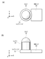
- FIG. 1 is a diagram illustrating a Cu pillar, in which (a) is a top view and (b) is a side view.
- FIG. 2 is a diagram showing a test pattern according to an embodiment of the present disclosure, in which (a) is a top view and (b) is a side view.
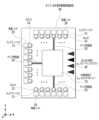
- FIG. 3 is a diagram showing a schematic configuration of an optical semiconductor integrated circuit according to an embodiment of the present disclosure.
- FIG. 4 is a diagram illustrating a state in which a chip having a Cu pillar according to an embodiment of the present disclosure is mounted on an external package board or a circuit board.
- FIG. 5 is a diagram illustrating a state in which a chip having Cu pillars is mounted on an external package board or circuit board.
- FIG. 6 is a diagram showing a schematic configuration of an optical semiconductor integrated circuit according to an embodiment of the present disclosure.
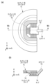
- FIG. 7 is a diagram showing a cantilever probe card and a chip during automatic wafer level inspection, in which (a) is a top view and (b) is a side view.
- FIG. 8 is a diagram showing the state in which the tip of the cantilever probe is in contact with the test pad 20.
- (a) is a diagram showing a (newer) cantilever probe with less wear on the tip, and
- (b) is a diagram showing the tip of the needle.
- FIG. 3 is a diagram showing a cantilever probe with many scratches.
- FIG. 9 is a diagram showing a schematic configuration of an optical semiconductor integrated circuit according to an embodiment of the present disclosure.
- FIG. 10 is a diagram showing a schematic configuration of an optical semiconductor integrated circuit according to an embodiment of the present disclosure.
- FIG. 11 is a diagram showing a schematic configuration of an optical semiconductor integrated circuit according to an embodiment of the
- an optical semiconductor integrated circuit according to an embodiment of the present disclosure will be described in detail with reference to the drawings.
- the same or similar symbols indicate the same or similar elements, and repeated description may be omitted.
- an optical semiconductor integrated circuit is an integrated circuit that includes an optical circuit
- the present disclosure can also be explained using a semiconductor integrated circuit that does not include an optical circuit instead of the optical semiconductor integrated circuit.
- FIG. 1 is a diagram illustrating a Cu pillar, in which (a) is a top view and (b) is a side view.
- An optical semiconductor integrated circuit including an optical circuit according to an embodiment of the present disclosure can also use Cu pillars to achieve higher terminal density and narrower pad pitch.
- the Cu pillar 10 is formed on a Cu pillar pad 11.
- the Cu pillar 10 has a cylindrical shape and has a circular cross section in the horizontal direction (XY plane direction).
- the Cu pillar pad 11 also has a cylindrical shape, and the diameter of the horizontal cross section is larger than the diameter of the Cu pillar 10.
- Solder 12 is arranged on the upper surface of the Cu pillar 10. In a top view, the Cu pillar 10 is located inside the Cu pillar pad 11. The solder 12 on the upper surface of the Cu pillar 10 forms a bump.
- FIG. 2 is a diagram showing a test pattern, in which (a) is a top view and (b) is a side view.
- the inspection pattern shown in FIG. 2 is formed in an optical semiconductor integrated circuit on a wafer and used in automatic wafer level inspection of the optical semiconductor integrated circuit.
- the inspection pattern includes a Cu pillar pad 11, a Cu pillar 10 disposed on the Cu pillar pad 11, and an inspection pad 20 overlapping the Cu pillar pad 11.
- the test pad 20 provides a contact area for cantilever probes placed on a cantilever probe card during wafer level automatic testing.
- the Cu pillar pad 11 and the test pad 20 only need to be arranged adjacent to each other, and the Cu pillar pad 11 and the test pad 20 do not need to have an overlapping region in the Z-axis direction.
- the Cu pillar pad 11 and the test pad 20 can be formed as one continuous region by the same manufacturing process.
- solder 12 is also shown on the top surface of the Cu pillar 10. Solder 12 constitutes a bump in the flip-chip connection.
- cantilever probes are attached to the Cu pillar 10, Cu pillar pad 11, and solder 12 during wafer level automatic inspection. There is no need to make contact. Therefore, no contact marks are generated on the Cu pillar 10, the Cu pillar pad 11, and the solder 12.
- the present invention is applicable not only to optical semiconductor integrated circuit wafers but also to semiconductor integrated circuit wafers that do not include optical circuits. That is, by providing a test pattern including test pads on a semiconductor integrated circuit wafer, automatic wafer level testing using a cantilever probe card becomes possible. By using a cantilever probe card, which costs less than a vertical probe card, inspection can be carried out at a lower cost.
- FIG. 3 shows one of a plurality of optical semiconductor integrated circuits formed on a wafer.
- An optical semiconductor integrated circuit is an integrated circuit that includes an optical circuit, and is formed on a wafer.
- an optical semiconductor integrated circuit is cut out from a wafer as a chip containing one optical semiconductor integrated circuit after automatic wafer level inspection. Chips cut from the wafer are modularized with other parts to form an optical communication module.
- the optical semiconductor integrated circuit shown in FIG. 3 includes a rectangular chip 30 (that is, an optical semiconductor integrated circuit board), an optical input/output terminal 32 and a semiconductor element 31 formed on the main surface (XY plane) of the chip 30, and a plurality of semiconductor elements 31. and an in-chip wiring 33 that electrically connects each of the plurality of test patterns and the semiconductor element 31.
- Each of the plurality of test patterns formed on the chip 30 has the test pattern described with reference to FIG. 2, that is, the Cu pillar pad 11, the Cu pillar 10, the test pad 20, and the solder 12.
- the test pad 20 arranged adjacent to the Cu pillar pad 11 is electrically connected to the semiconductor element 31 by an intra-chip wiring 33 .
- the test pad 20 provides a contact area for cantilever probes disposed on the cantilever probe card during wafer level automatic testing performed before the chips 30 are cut from the wafer.
- the Cu pillar pad 11, the Cu pillar 10, and the solder 12 are connected to, for example, a driver IC of the semiconductor device 31, a bias circuit, a transimpedance amplifier (TIA), and other elements such as a wiring board and a radio frequency (RF) wiring board. (not shown) to provide a connection point for flip-connecting the chip 30 to one or more of the following: (not shown).
- a plurality of inspection patterns are linearly arranged near the end face of the rectangular chip 30, that is, near the outer periphery of the chip 30.
- the Cu pillar pad 11 of each inspection pattern is arranged closer to the end surface than the inspection pad 20.
- the test pads 20 of each test pattern are arranged in a direction away from the end face closest to the Cu pillar pad 11 (in a direction toward the end face opposite to the nearest end face).
- a Cu pillar 10 is arranged on the Cu pillar pad 11, and a solder 12 is arranged on the upper surface of the Cu pillar 10. In FIG. 3, the Cu pillar 10 is located below the solder 12.
- the optical input/output terminal 32 is, for example, a grating coupler, and is an optical circuit integrated on the chip 30.
- the semiconductor element 31 is, for example, a photodiode, and is an optical circuit integrated on the chip 30.
- the semiconductor element 31 of the chip 30 of this embodiment is a photodiode
- a bias is applied to the photodiode of the chip 30 in the optical communication module via the Cu pillar 10 from an external bias source, and an input voltage is applied via the grating coupler to the photodiode of the chip 30. It operates to photoelectrically convert light from other optical circuits and supply electrical signals to an external TIA via the Cu pillar 10.
- the photodiode of the chip 30 receives a bias from the inspection equipment via the cantilever probe in contact with the inspection pad 20, and photoelectrically converts the light from the optical probe that is incident via the grating coupler.
- the test pad 20 operates to supply an electrical signal to the test device via the cantilever probe that is in contact with the test pad 20.
- the semiconductor element 31 of the chip 30 of this embodiment is a laser diode
- the laser diode of the chip 30 is connected to the Cu pillar 10 from an external driver IC (or an RF wiring board connected to an external driver IC) in the optical communication module.
- a control signal is supplied through the grating coupler, and the grating coupler operates to output an optical signal to another optical circuit.
- the laser diode of the chip 30 is supplied with a control signal from the inspection equipment via a cantilever probe in contact with the inspection pad 20, and the optical signal from the optical probe is sent to the inspection equipment via the grating coupler. Operate to supply.
- the optical modulator of the chip 30 is connected to an external driver IC (or an RF wiring board connected to an external driver IC) in the optical communication module.
- a modulation signal is provided through the pillar 10 to modulate the optical signal from another optical circuit entering through one part of the grating coupler and to another optical circuit through another part of the grating coupler. It operates to emit a modulated optical signal.
- the optical modulator of the chip 30 is supplied with a modulation signal from the inspection equipment via the cantilever probe in contact with the inspection pad 20, and modulates the optical signal incident from the optical probe via the grating coupler. and supplies it to the inspection device via another optical probe.
- the test pads 20 are arranged at the periphery of the chip, and the optical circuits (photodiode, laser diode, etc.) are arranged at the center of the chip. or an optical modulator, etc.) are arranged.
- semiconductor elements that constitute an electronic circuit transistor that constitute an amplifier, driver IC, etc. are placed in the center of the chip. ) is placed.
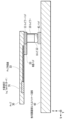
- FIG. 4 is a diagram illustrating a state in which the chip 30 is flip-chip mounted on an external package board or circuit board 40 using the Cu pillar 10. As shown in FIG. 4, no stub (open) occurs in the electrical signal path between the external circuit board 40 and the semiconductor element 31 included in the chip 30.
- FIG. 5 is a diagram illustrating a state in which a chip 50 in which the arrangement of the Cu pillar pad 11 and the inspection pad 20 in the inspection pattern of the chip 30 in FIG.
- the test pad 20 located closer to the end surface than the Cu pillar pad 11 acts as a stub, which causes deterioration of high frequency characteristics.
- FIG. 6 shows one of a plurality of optical semiconductor integrated circuits formed on a wafer.
- the test pads 20 are arranged at the periphery of the chip in order to reduce the size of the chip 60, similarly to the optical semiconductor integrated circuit described above.
- the rectangular chip 60 shown in FIG. 6 differs from the chip 30 shown in FIG. 3 in the arrangement of the plurality of test patterns formed on the chip 60. More specifically, as shown in FIG. 6, in the chip 60, the test pads 20 of each test pattern were arranged closer to the end surface than the Cu pillar pads 11, and were arranged adjacent to the test pads 20.
- This chip differs from the chip 30 shown in FIG. 3 in that the Cu pillar pad 11 is electrically connected to the semiconductor element 31 by an intra-chip wiring 33.
- FIG. 7 is a diagram showing a cantilever probe card and a chip during automatic wafer level inspection, with (a) being a top view and (b) being a side view.
- a cantilever probe card 71 shown in FIG. 7 has an opening larger than the size of the chip 70 to be inspected, and cantilever probes 72 are arranged around the opening.
- FIG. 7 also shows an optical probe 73 for testing the input/output of light to the chip 70 to be tested.
- the cantilever probe 72 enters the periphery of the chip 70 from the outer periphery of the chip toward the inside of the chip for inspection. make contact with the pad.
- the cantilever probe card is cleaned after the inspection is completed. This cleaning involves abrasion of the tip of the cantilever probe.
- FIG. 8 is a diagram showing a state in which the tip of the cantilever probe is in contact with the test pad 20 in the inspection pattern of the present disclosure, and (a) shows a (newer) cantilever probe with less wear on the tip.
- FIG. 2B shows a cantilever probe with a needle tip that is often scratched. As shown in FIG. 8B, if much of the needle tip is shaved off by cleaning, the cantilever probe 72 approaches the Cu pillar 10 (and the solder 12) during automatic wafer level inspection. If the cantilever probe 72 collides with the Cu pillar 10 (and the solder 12), it will cause damage.
- the size of the test pad 20 in advance, taking into account the margin due to scraping of the needle tip.
- the diameter of a typical Cu pillar is 60 ⁇ m, and considering the manufacturing error of the cantilever probe and the probing accuracy of the inspection device, the Cu pillar 10 and the cantilever probe 72 need to be separated by about 30 ⁇ m even after the cleaning operation. There is. Then, the initial size of the test pad 20 needs to be approximately 125 ⁇ m in length in the direction in which the cantilever probe 72 skates.
- the optical semiconductor integrated circuit according to the embodiment shown in FIG. 6 by arranging the test pad 20 at a position closer to the end surface of the chip 60 than the Cu pillar pad 11, the tip of the cantilever probe 72 is removed by cleaning. Even if it is scraped, it will not come close to the Cu pillar 10 (and solder 12). Therefore, the length in the skating direction of the cantilever probe 72 of the size of the test pad 20 can eliminate a margin of 20 ⁇ m due to abrasion of the needle tip. That is, the test pad 20 can be smaller in size than the example described above with reference to FIG. 8. As a result, by reducing the capacitance component of the test pad 20, the optical semiconductor integrated circuit or It becomes possible to provide a semiconductor integrated circuit.
- FIG. 9 shows one of a plurality of optical semiconductor integrated circuits formed on a wafer.
- the test pads 20 are arranged at the periphery of the chip in order to reduce the size of the chip 60, similarly to the optical semiconductor integrated circuit described above.
- the rectangular chip 90 shown in FIG. 9 differs from the chip 30 shown in FIG. 3 in the arrangement of the plurality of test patterns formed on the chip 90. More specifically, as shown in FIG. 9, in the chip 60, the test pads 20 and Cu pillar pads 11 of each test pattern are arranged parallel to the nearest end surface, and are arranged adjacent to the test pads 20.
- the chip 30 differs from the chip 30 shown in FIG. 3 in that the Cu pillar pad 11 is electrically connected to the semiconductor element 31 by an intra-chip wiring 33.
- test pad 20 can be smaller in size than the example described above with reference to FIG. 8. As a result, by reducing the capacitance component of the test pad 20, the optical semiconductor integrated circuit or It becomes possible to provide a semiconductor integrated circuit.
- FIG. 10 shows one of a plurality of optical semiconductor integrated circuits formed on a wafer.
- the optical semiconductor integrated circuit shown in FIG. 10 includes a rectangular chip 100 (that is, an optical semiconductor integrated circuit board), a semiconductor element 31 formed on the main surface (XY plane) of the chip 100, and a plurality of inspection patterns. It includes a high frequency wiring 101 that electrically connects each of the plurality of inspection patterns and the semiconductor element 31.
- the two high-frequency wires 101 in FIG. 10 are just an example, and the number of high-frequency wires 101 included in the optical semiconductor integrated circuit, that is, the number of inspection patterns is not limited to two.
- the optical semiconductor integrated circuit can include the number of high-frequency wiring lines 101 depending on a desired configuration such as an SGS configuration or a GSGSG configuration.
- the inspection pattern in the optical semiconductor integrated circuit according to this embodiment includes a Cu pillar pad 11, a Cu pillar 10, a solder 12, and an inspection pad window 102.
- the in-chip wiring 33 connecting the Cu pillar pad 11 and the semiconductor element 31 is configured as a high-frequency wiring 101, and the test pad window 102 is provided on the high-frequency wiring 111 as described with reference to FIG. Different from the inspection pattern.
- the test pad window 102 is a portion from which the passivation film formed on the top surface of the chip 100 is removed.
- the test pad window 102 is rectangular like the test pad 20.
- the test pad window 102 corresponds to the above-described test pad 20, and provides an area with which a cantilever probe placed on a cantilever probe card comes into contact during wafer level automatic testing.
- test pad window 102 of each test pattern is arranged in a direction away from the end face closest to the Cu pillar pad 11 (in a direction toward the end face opposite to the nearest end face). ing.
- the optical semiconductor integrated circuit is capable of performing automatic wafer level inspection using the test pad window 102 and a low-cost cantilever probe card, which eliminates the increase in capacity due to the accompanying test pad and the accompanying deterioration of high frequency characteristics.
- a circuit or a semiconductor integrated circuit can be provided.
- FIG. 11 shows one of a plurality of optical semiconductor integrated circuits formed on a wafer.
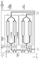
- the optical semiconductor integrated circuit shown in FIG. 11 includes a rectangular chip 110 (that is, an optical semiconductor integrated circuit board), two semiconductor elements 31a and 31b formed on the main surface (XY plane) of the chip 110, and multiple inspections. and high-frequency wiring 111 that electrically connects each of the plurality of inspection patterns and the semiconductor elements 31a and 31b. As described above with reference to FIG. 10, the number of high-frequency wirings 111 in the chip 110 of FIG. obtain.
- the semiconductor element 31a has a configuration in which a child Mach-Zehnder is placed in each of two arm optical waveguides that constitute one parent Mach-Zehnder.
- the configuration of the semiconductor element 31b is similar to that of the semiconductor element 31a.
- the two semiconductor elements 31a and 31b are arranged in parallel and are configured such that one branched from the input light is modulated by the semiconductor element 31a, and the other is modulated by the semiconductor element 31b.
- the optical waveguide 112 shown in FIG. 11 is a waveguide path through which input light is modulated and output.
- the test pattern for the optical semiconductor integrated circuit according to this embodiment includes a Cu pillar pad 11, a Cu pillar 10, a solder 12, and a test pad window 102, similar to the test pattern in FIG.
- the intra-chip wiring 33 connecting the Cu pillar pad 11 and the semiconductor element 31 is configured as a high frequency wiring 111, and a test pad window 102 is provided on the high frequency wiring 111.
- an optical waveguide 112 that intersects with the high-frequency interconnect 111 is located below the high-frequency interconnect 111 between the Cu pillar pad 11 and the inspection pad window 102. It is different from the inspection pattern described with reference to FIG. 10 in that it is formed.
- optical waveguides generally occupy much of the space on a chip. Furthermore, since electrical elements (transistors) and optical semiconductor elements (optical modulators, photodiodes) are present inside the chip, it may be difficult to secure space for the optical waveguide. Therefore, in this embodiment, the optical waveguide 112 is arranged at the outer periphery of the chip 110 in order to reduce the area of the chip 110.
- the strain stress generated on the Cu pillar 10 after flip-chip mounting will be affected by the wavelength characteristics of the optical waveguide 112, which will also affect the performance of the optical circuit. There is. Furthermore, even if there is an optical waveguide in the lower layer of the test pad 20, the stress caused by the cantilever probe during automatic wafer level inspection may damage the optical waveguide 112 and affect its characteristics, such as an increase in loss characteristics. There is. For this reason, the optical waveguide 112 cannot be placed below the Cu pillar 10 and the inspection pad 20.
- the optical waveguide 112 is arranged at the outer periphery of the chip 110, excluding the lower layer where stress is applied (for example, the Cu pillar 10, the test pad 20, and the test pad window 102).
- the characteristics of the optical waveguide or the performance of the optical circuit are prevented from deteriorating, and the size of the chip 110 is reduced, and the test pad and the low-cost cantilever probe card are used. It is possible to provide an optical semiconductor integrated circuit or a semiconductor integrated circuit that is capable of automatic wafer level inspection.
- an optical semiconductor integrated circuit or a semiconductor integrated circuit that can perform automatic wafer level inspection using a low-cost cantilever probe card.
Landscapes
- Engineering & Computer Science (AREA)
- Computer Hardware Design (AREA)
- Microelectronics & Electronic Packaging (AREA)
- General Engineering & Computer Science (AREA)
- Physics & Mathematics (AREA)
- General Physics & Mathematics (AREA)
- Testing Or Measuring Of Semiconductors Or The Like (AREA)
- Measuring Leads Or Probes (AREA)
Abstract
Description
図2を参照して本開示の第1の実施形態に係る検査用のパターンを説明する。図2は検査用のパターンを示す図であり、(a)は上面図であり、(b)は側面図である。図2に示す検査用のパターンは、ウェハ上の光半導体集積回路内に形成され、当該光半導体集積回路のウェハレベル自動検査において使用される。
図3、4および5を参照して本開示の第2の実施形態に係る光半導体集積回路を説明する。図3は、ウェハ上に形成された複数の光半導体集積回路のうちの1つを示している。光半導体集積回路は、光回路を含む集積回路であり、ウェハ上に形成される。上述したように、光半導体集積回路はウェハレベル自動検査の後に、ウェハから1つの光半導体集積回路を含むチップとして切り出される。ウェハから切り出されたチップは、他の部品と共にモジュール化されて、光通信モジュールを構成する。
図6を参照して本開示の第3の実施形態に係る光半導体集積回路を説明する。図6は、図3と同様に、ウェハ上に形成された複数の光半導体集積回路のうちの1つを示している。本実施形態に係る光半導体集積回路においても、前述した光半導体集積回路と同様に、チップ60のサイズを小型化するために、チップの周辺部に検査パッド20は配置される。図6に示す矩形のチップ60は、図3に示すチップ30と比較して、チップ60に形成された複数の検査用パターンの配置が異なる。より具体的には、図6に示すようにチップ60は、各検査用パターンの検査パッド20が、Cuピラーパッド11よりも端面に近い位置に配置され、検査パッド20と隣接して配置されたCuピラーパッド11がチップ内配線33により半導体素子31と電気的に接続されている点で、図3に示すチップ30と異なる。
図9を参照して本開示の第4の実施形態に係る光半導体集積回路を説明する。図9は、図3と同様に、ウェハ上に形成された複数の光半導体集積回路のうちの1つを示している。本実施形態に係る光半導体集積回路においても、前述した光半導体集積回路と同様に、チップ60のサイズを小型化するために、チップの周辺部に検査パッド20は配置される。図9に示す矩形のチップ90は、図3に示すチップ30と比較して、チップ90に形成された複数の検査用パターンの配置が異なる。より具体的には、図9に示すようにチップ60は、各検査用パターンの検査パッド20およびCuピラーパッド11が、最も近い端面に対して平行に配置され、検査パッド20と隣接して配置されたCuピラーパッド11がチップ内配線33により半導体素子31と電気的に接続されている点で、図3に示すチップ30と異なる。
図10を参照して本開示の第5の実施形態に係る光半導体集積回路を説明する。図10は、図3と同様に、ウェハ上に形成された複数の光半導体集積回路のうちの1つを示している。図10に示す光半導体集積回路は、矩形のチップ100(すなわち、光半導体集積回路基板)と、チップ100の主面(XY面)に形成された半導体素子31と、複数の検査用パターンと、複数の検査用パターンの各々と半導体素子31とを電気的に接続する高周波配線101とを備える。図10における2つの高周波配線101は例示であって、光半導体集積回路が備える高周波配線101の数、すなわち検査用パターンの数は2つに限られない。信号線およびグランド線をそれぞれSおよびGとして、光半導体集積回路は、SGS構成またはGSGSG構成などの所望の構成に応じた数の高周波配線101を含み得る。
図11を参照して本開示の第6の実施形態に係る光半導体集積回路を説明する。図11は、図3と同様に、ウェハ上に形成された複数の光半導体集積回路のうちの1つを示している。図11に示す光半導体集積回路は、矩形のチップ110(すなわち、光半導体集積回路基板)と、チップ110の主面(XY面)に形成された2つの半導体素子31aおよび31bと、複数の検査用パターンと、複数の検査用パターンの各々と半導体素子31aおよび31bとを電気的に接続する高周波配線111とを備える。図10を参照して上述したように、図11のチップ110においても、高周波配線111の数は例示であって、SGS構成またはGSGSG構成などの所望の構成に応じた数の高周波配線111を含み得る。
11 Cuピラーパッド
12 はんだ
20 検査パッド
30、50、60、70、90、100、110 チップ(光半導体集積基板)
31 半導体素子(フォトダイオード、光変調器)
32 光入出力端子(グレーティングカプラ)
33 チップ内配線
40 外部回路(またはパッケージ基板)
41 パッド
71 カンチレバー型プローブカード
72 カンチレバー型プローブ
73 光プローブ
101、111 高周波配線
102 検査パッドウインドウ
112 光導波路
Claims (8)
- 検査用パターンであって、
半導体集積基板上に形成されたCuピラーパッドと、
前記Cuピラーパッド上に形成されたCuピラーと、
前記半導体集積基板上に形成された検査パッドであって、前記Cuピラーパッドと隣接または近接し電気的に結合されており、ウェハレベル自動検査の際にカンチレバー型プローブがコンタクトする領域を提供する、検査パッドと
を備えた、検査用パターン。 - 前記検査用パターンは前記半導体集積基板の外周の近傍に配置されており、
前記検査パッドよりも前記半導体集積基板の前記外周に近い位置に前記Cuピラーパッドが配置されている、請求項1に記載の検査用パターン。 - 前記検査用パターンは前記半導体集積基板の外周の近傍に配置されており、
前記Cuピラーパッドよりも前記半導体集積基板の前記外周に近い位置に前記検査パッドが配置されている、請求項1に記載の検査用パターン。 - 前記検査用パターンは前記半導体集積基板の外周の近傍に配置されており、
前記Cuピラーパッドおよび前記Cuピラーパッドと隣接または近接し電気的に結合された前記検査パッドが、前記半導体集積基板の前記外周に対して平行に配置されている、請求項1に記載の検査用パターン。 - 前記検査用パターンは前記半導体集積基板の外周の近傍に配置されており、
前記検査パッドは、前記半導体集積基板上に形成された高周波配線上に形成されており、前記高周波配線は、前記Cuピラーパッドと半導体素子とを結合し、前記Cuピラーと前記半導体素子との間で高周波電気信号を伝搬する、請求項1に記載の検査用パターン。 - 前記Cuピラーパッドと前記検査パッドとの間に形成された光導波路をさらに備え、
前記Cuピラーパッドと前記検査パッドとの間の前記高周波配線が前記光導波路と交差する、請求項5に記載の検査用パターン。 - 請求項1に記載の検査用パターンと
前記半導体集積基板上に形成された、半導体素子と、
を備えた半導体集積回路。 - 請求項1に記載の検査用パターンと、
前記半導体集積基板上に形成された、光回路を含む光半導体素子と、
を備えた光半導体集積回路。
Priority Applications (3)
| Application Number | Priority Date | Filing Date | Title |
|---|---|---|---|
| US18/993,106 US20260033296A1 (en) | 2022-07-27 | 2022-07-27 | Inspection Pattern and Semiconductor Integrated Circuit Therewith |
| JP2024536634A JP7791489B2 (ja) | 2022-07-27 | 2022-07-27 | 検査用パターンおよびそれを備えた半導体集積回路 |
| PCT/JP2022/028926 WO2024023969A1 (ja) | 2022-07-27 | 2022-07-27 | 検査用パターンおよびそれを備えた半導体集積回路 |
Applications Claiming Priority (1)
| Application Number | Priority Date | Filing Date | Title |
|---|---|---|---|
| PCT/JP2022/028926 WO2024023969A1 (ja) | 2022-07-27 | 2022-07-27 | 検査用パターンおよびそれを備えた半導体集積回路 |
Publications (1)
| Publication Number | Publication Date |
|---|---|
| WO2024023969A1 true WO2024023969A1 (ja) | 2024-02-01 |
Family
ID=89705835
Family Applications (1)
| Application Number | Title | Priority Date | Filing Date |
|---|---|---|---|
| PCT/JP2022/028926 Ceased WO2024023969A1 (ja) | 2022-07-27 | 2022-07-27 | 検査用パターンおよびそれを備えた半導体集積回路 |
Country Status (3)
| Country | Link |
|---|---|
| US (1) | US20260033296A1 (ja) |
| JP (1) | JP7791489B2 (ja) |
| WO (1) | WO2024023969A1 (ja) |
Citations (11)
| Publication number | Priority date | Publication date | Assignee | Title |
|---|---|---|---|---|
| JP2003249534A (ja) * | 2002-02-25 | 2003-09-05 | Matsushita Electric Ind Co Ltd | 高周波回路、高周波回路装置 |
| JP2004020708A (ja) * | 2002-06-13 | 2004-01-22 | Hitachi Ltd | 進行波型光変調装置 |
| JP2005308558A (ja) * | 2004-04-22 | 2005-11-04 | National Institute Of Advanced Industrial & Technology | システムインパッケージ試験検査装置および試験検査方法 |
| JP2011103334A (ja) * | 2009-11-10 | 2011-05-26 | Renesas Electronics Corp | 半導体装置及び半導体装置の製造方法 |
| JP2012023065A (ja) * | 2010-07-12 | 2012-02-02 | Nippon Telegr & Teleph Corp <Ntt> | 半導体素子 |
| JP2014164272A (ja) * | 2013-02-27 | 2014-09-08 | Furukawa Electric Co Ltd:The | 光導波回路、および、光導波回路への電流印加方法 |
| JP2014229632A (ja) * | 2013-05-17 | 2014-12-08 | 住友電気工業株式会社 | 半導体装置 |
| JP2015046569A (ja) * | 2013-07-31 | 2015-03-12 | マイクロン テクノロジー, インク. | 半導体装置の製造方法 |
| JP2018163216A (ja) * | 2017-03-24 | 2018-10-18 | 住友大阪セメント株式会社 | 光変調器 |
| JP2018189699A (ja) * | 2017-04-28 | 2018-11-29 | 日本電信電話株式会社 | 光送信器 |
| WO2022024276A1 (ja) * | 2020-07-29 | 2022-02-03 | 日本電信電話株式会社 | 半導体光変調器 |
-
2022
- 2022-07-27 JP JP2024536634A patent/JP7791489B2/ja active Active
- 2022-07-27 US US18/993,106 patent/US20260033296A1/en active Pending
- 2022-07-27 WO PCT/JP2022/028926 patent/WO2024023969A1/ja not_active Ceased
Patent Citations (11)
| Publication number | Priority date | Publication date | Assignee | Title |
|---|---|---|---|---|
| JP2003249534A (ja) * | 2002-02-25 | 2003-09-05 | Matsushita Electric Ind Co Ltd | 高周波回路、高周波回路装置 |
| JP2004020708A (ja) * | 2002-06-13 | 2004-01-22 | Hitachi Ltd | 進行波型光変調装置 |
| JP2005308558A (ja) * | 2004-04-22 | 2005-11-04 | National Institute Of Advanced Industrial & Technology | システムインパッケージ試験検査装置および試験検査方法 |
| JP2011103334A (ja) * | 2009-11-10 | 2011-05-26 | Renesas Electronics Corp | 半導体装置及び半導体装置の製造方法 |
| JP2012023065A (ja) * | 2010-07-12 | 2012-02-02 | Nippon Telegr & Teleph Corp <Ntt> | 半導体素子 |
| JP2014164272A (ja) * | 2013-02-27 | 2014-09-08 | Furukawa Electric Co Ltd:The | 光導波回路、および、光導波回路への電流印加方法 |
| JP2014229632A (ja) * | 2013-05-17 | 2014-12-08 | 住友電気工業株式会社 | 半導体装置 |
| JP2015046569A (ja) * | 2013-07-31 | 2015-03-12 | マイクロン テクノロジー, インク. | 半導体装置の製造方法 |
| JP2018163216A (ja) * | 2017-03-24 | 2018-10-18 | 住友大阪セメント株式会社 | 光変調器 |
| JP2018189699A (ja) * | 2017-04-28 | 2018-11-29 | 日本電信電話株式会社 | 光送信器 |
| WO2022024276A1 (ja) * | 2020-07-29 | 2022-02-03 | 日本電信電話株式会社 | 半導体光変調器 |
Also Published As
| Publication number | Publication date |
|---|---|
| JP7791489B2 (ja) | 2025-12-24 |
| US20260033296A1 (en) | 2026-01-29 |
| JPWO2024023969A1 (ja) | 2024-02-01 |
Similar Documents
| Publication | Publication Date | Title |
|---|---|---|
| US12332297B2 (en) | Test system | |
| TWI761691B (zh) | 用於pic晶粒之探針以及相關測試組件與方法 | |
| US7927898B2 (en) | Apparatus and methods for packaging electronic devices for optical testing | |
| US11714239B2 (en) | Optical device for coupling light | |
| WO2011055511A1 (ja) | 半導体装置及びその製造方法 | |
| TWI773248B (zh) | 半導體結構及其形成方法 | |
| JP2006504255A (ja) | 直接接続光受信モジュールおよびその試験方法 | |
| JPS6231136A (ja) | 光半導体素子の評価装置 | |
| JP7791489B2 (ja) | 検査用パターンおよびそれを備えた半導体集積回路 | |
| US6555841B1 (en) | Testable substrate and a testing method | |
| JP3310930B2 (ja) | プローブカード | |
| US6707679B2 (en) | Butt joined opto-electronic module | |
| JP7839427B2 (ja) | 光半導体集積回路 | |
| JP2011081115A (ja) | 半導体パッケージ、半導体装置、及びその検査方法 | |
| US12449618B2 (en) | Low-loss coplanar waveguide bonding structure and manufacturing method thereof | |
| US20250149520A1 (en) | Semiconductor package | |
| JP4418883B2 (ja) | 集積回路チップの試験検査装置、集積回路チップの試験検査用コンタクト構造体及びメッシュコンタクト | |
| US8139949B2 (en) | Electrical signal transmission module, method of transmitting electric signals and electrical inspection apparatus having the same | |
| JP2020166158A (ja) | 光導波路素子、及び光導波路デバイス | |
| US6726377B2 (en) | Butt joined electrical apparatus and module | |
| US6827504B2 (en) | Butt joined electronic assembly and module having an electrical standoff | |
| US6722795B2 (en) | Butt joined opto-electrical apparatus and module | |
| KR200486147Y1 (ko) | 웨이퍼를 테스트하는 프로브카드 및 그것의 인쇄회로기판 | |
| JP2023175292A (ja) | プローブシート、検査装置、検査方法および検査プログラム | |
| JPH06349970A (ja) | 伝送線路基板及び伝送線路基板を用いた半導体基板実装方法 |
Legal Events
| Date | Code | Title | Description |
|---|---|---|---|
| 121 | Ep: the epo has been informed by wipo that ep was designated in this application |
Ref document number: 22953064 Country of ref document: EP Kind code of ref document: A1 |
|
| WWE | Wipo information: entry into national phase |
Ref document number: 2024536634 Country of ref document: JP |
|
| WWE | Wipo information: entry into national phase |
Ref document number: 18993106 Country of ref document: US |
|
| NENP | Non-entry into the national phase |
Ref country code: DE |
|
| 122 | Ep: pct application non-entry in european phase |
Ref document number: 22953064 Country of ref document: EP Kind code of ref document: A1 |
|
| WWP | Wipo information: published in national office |
Ref document number: 18993106 Country of ref document: US |