WO2024019098A1 - 半導体発光素子及び半導体発光素子の製造方法 - Google Patents
半導体発光素子及び半導体発光素子の製造方法 Download PDFInfo
- Publication number
- WO2024019098A1 WO2024019098A1 PCT/JP2023/026476 JP2023026476W WO2024019098A1 WO 2024019098 A1 WO2024019098 A1 WO 2024019098A1 JP 2023026476 W JP2023026476 W JP 2023026476W WO 2024019098 A1 WO2024019098 A1 WO 2024019098A1
- Authority
- WO
- WIPO (PCT)
- Prior art keywords
- layer
- light emitting
- iii
- type
- compound semiconductor
- Prior art date
- Legal status (The legal status is an assumption and is not a legal conclusion. Google has not performed a legal analysis and makes no representation as to the accuracy of the status listed.)
- Ceased
Links
Images

Classifications
-
- H—ELECTRICITY
- H10—SEMICONDUCTOR DEVICES; ELECTRIC SOLID-STATE DEVICES NOT OTHERWISE PROVIDED FOR
- H10H—INORGANIC LIGHT-EMITTING SEMICONDUCTOR DEVICES HAVING POTENTIAL BARRIERS
- H10H20/00—Individual inorganic light-emitting semiconductor devices having potential barriers, e.g. light-emitting diodes [LED]
- H10H20/80—Constructional details
- H10H20/81—Bodies
- H10H20/822—Materials of the light-emitting regions
- H10H20/824—Materials of the light-emitting regions comprising only Group III-V materials, e.g. GaP
-
- H—ELECTRICITY
- H10—SEMICONDUCTOR DEVICES; ELECTRIC SOLID-STATE DEVICES NOT OTHERWISE PROVIDED FOR
- H10H—INORGANIC LIGHT-EMITTING SEMICONDUCTOR DEVICES HAVING POTENTIAL BARRIERS
- H10H20/00—Individual inorganic light-emitting semiconductor devices having potential barriers, e.g. light-emitting diodes [LED]
- H10H20/80—Constructional details
- H10H20/81—Bodies
- H10H20/811—Bodies having quantum effect structures or superlattices, e.g. tunnel junctions
- H10H20/812—Bodies having quantum effect structures or superlattices, e.g. tunnel junctions within the light-emitting regions, e.g. having quantum confinement structures
-
- H—ELECTRICITY
- H10—SEMICONDUCTOR DEVICES; ELECTRIC SOLID-STATE DEVICES NOT OTHERWISE PROVIDED FOR
- H10H—INORGANIC LIGHT-EMITTING SEMICONDUCTOR DEVICES HAVING POTENTIAL BARRIERS
- H10H20/00—Individual inorganic light-emitting semiconductor devices having potential barriers, e.g. light-emitting diodes [LED]
- H10H20/01—Manufacture or treatment
- H10H20/011—Manufacture or treatment of bodies, e.g. forming semiconductor layers
- H10H20/013—Manufacture or treatment of bodies, e.g. forming semiconductor layers having light-emitting regions comprising only Group III-V materials
-
- H—ELECTRICITY
- H10—SEMICONDUCTOR DEVICES; ELECTRIC SOLID-STATE DEVICES NOT OTHERWISE PROVIDED FOR
- H10H—INORGANIC LIGHT-EMITTING SEMICONDUCTOR DEVICES HAVING POTENTIAL BARRIERS
- H10H20/00—Individual inorganic light-emitting semiconductor devices having potential barriers, e.g. light-emitting diodes [LED]
- H10H20/01—Manufacture or treatment
- H10H20/011—Manufacture or treatment of bodies, e.g. forming semiconductor layers
- H10H20/019—Removal of at least a part of a substrate on which semiconductor layers have been formed
-
- H—ELECTRICITY
- H10—SEMICONDUCTOR DEVICES; ELECTRIC SOLID-STATE DEVICES NOT OTHERWISE PROVIDED FOR
- H10H—INORGANIC LIGHT-EMITTING SEMICONDUCTOR DEVICES HAVING POTENTIAL BARRIERS
- H10H20/00—Individual inorganic light-emitting semiconductor devices having potential barriers, e.g. light-emitting diodes [LED]
- H10H20/80—Constructional details
- H10H20/81—Bodies
- H10H20/815—Bodies having stress relaxation structures, e.g. buffer layers
Definitions
- the present invention relates to a semiconductor light emitting device and a method for manufacturing a semiconductor light emitting device.
- Group III-V compound semiconductors such as InGaAsP, InGaAlAs, and InAsSbP are used as semiconductor materials for semiconductor layers in semiconductor light emitting devices.
- the composition ratio of the light-emitting layer formed of the III-V group compound semiconductor material it is possible to adjust the emission wavelength of the semiconductor light-emitting element over a wide range from green to infrared.
- infrared-emitting semiconductor light-emitting elements whose emission wavelength is in the infrared region of 750 nm or more are widely used in applications such as sensors, gas analysis, surveillance cameras, and communications.
- Patent Document 1 discloses a semiconductor light emitting device having a light emitting layer having a stacked structure in which a first III-V compound semiconductor layer and a second III-V compound semiconductor layer having different composition ratios are repeatedly stacked.
- the compositional wavelength difference between the compositional wavelength of the III-V compound semiconductor layer and the compositional wavelength of the second III-V compound semiconductor layer is 50 nm or less
- the first III-V compound semiconductor A light emitting device is described in which the ratio of the difference in lattice constant between the lattice constant of the layer and the lattice constant of the second group III-V compound semiconductor layer is 0.05% or more and 0.60% or less.
- the half-value width of the emission peak in the emission spectrum is required to use a specific wavelength. It is said that it is preferable that the distance is narrower.
- Semiconductor light-emitting devices are required to have good light-emitting characteristics in terms of both high light-emitting output and full width at half maximum (FWHM) of the light-emitting peak. Therefore, an object of the present invention is to obtain a semiconductor light-emitting device having better light-emitting characteristics than conventional light-emitting devices.
- a semiconductor light emitting device comprising a light emitting layer having a laminate in which a first III-V compound semiconductor layer and a second III-V compound semiconductor layer are repeatedly stacked,
- the group III element in the first and second group III-V compound semiconductor layers is one or more selected from the group consisting of Al, Ga, and In
- the group V element in the first and second group III-V compound semiconductor layers is one or more selected from the group consisting of As, Sb, and P;
- the compositional wavelength difference between the compositional wavelength of the first III-V compound semiconductor layer and the compositional wavelength of the second III-V compound semiconductor layer is 70 nm or more,
- the well depth (Dc) on the conduction band side in the band structure of the laminate is larger than the well depth (Dv) on the valence band side, and the well depth on the conduction band side is formed by the compositional wavelength difference.
- a semiconductor light emitting device characterized in that the ratio (Dc/(Dc+Dv)) of the conduction band side well depth (Dc) and the valence band side well depth (Dv) to the sum of the well depth (Dc) is 65% or more.
- a semiconductor light emitting device characterized in that the ratio (Dc/(Dc+Dv)) of the conduction band side well depth (Dc) and the valence band side well depth (Dv) to the sum of the well depth (Dc) is 65% or more.
- the absolute value of the difference between the two lattice constants in the lattice constant of the first III-V group compound semiconductor layer and the lattice constant of the second III-V group compound semiconductor layer is the average of the two lattice constants.
- Group V element in the first and second Group III-V compound semiconductor layers is one selected from the group consisting of As, Sb, and P.
- compositional wavelength difference between the first III-V group compound semiconductor layer and the second III-V compound semiconductor layer is 100 nm or more and 290 nm or less, according to (1) above.
- the semiconductor light emitting device according to any one of (4) to (4).
- a method for manufacturing the semiconductor light emitting device comprising: including a light emitting layer forming step of forming the light emitting layer, The light emitting layer forming step is performed by repeating the first step of forming the first III-V compound semiconductor layer and the second step of forming the second III-V compound semiconductor layer.
- the present invention it is possible to provide a semiconductor light emitting device with better light emitting characteristics than conventional light emitting devices, and a method for manufacturing the same.
- FIG. 3 is a diagram showing an example of a band structure in a light emitting layer of the present embodiment calculated using simulation software.
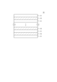
- 1 is a schematic cross-sectional view showing one embodiment of a light emitting layer in a semiconductor light emitting device according to the present invention.
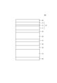
- 1 is a schematic cross-sectional view showing a semiconductor light emitting device according to an embodiment of the present invention.
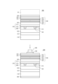
- 1 is a schematic cross-sectional view showing a method for manufacturing a semiconductor light emitting device according to an embodiment of the present invention using a bonding method.
- III-V compound semiconductor layer when simply referred to as a "III-V group compound semiconductor" in this specification, its composition is represented by the general formula: (In a Ga b Al c ) (P x As y Sb z ).
- the following relationship holds true regarding the composition ratio of each element.
- III-V compound semiconductor layer in the light emitting layer of the present invention is selected from the group consisting of one or more group III elements selected from the group consisting of Al, Ga, and In, and As, Sb, and P. Composed of one or more group V elements.
- the III-V compound semiconductor layer in the light emitting layer contains one or more group III elements selected from the group consisting of Al, Ga, and In, and one selected from the group consisting of As, Sb, and P.
- group III elements selected from the group consisting of Al, Ga, and In, and one selected from the group consisting of As, Sb, and P.
- the composition ratio of each element has the following relationship.
- group V elements one of x, y, and z is 1, and the other two are 0.
- the group III element is composed of two or more elements, and it is preferably composed using three types of elements. It is more preferable that The group V element of the III-V compound semiconductor layer in the light emitting layer preferably contains at least As or Sb. If the group III elements and group V elements are three or less elements in total, when trying to obtain a desired emission wavelength, the first layer and the second layer must have a composition ratio within the range of the present invention. The combination options are limited. Therefore, it is preferable that at least one of the first layer and the second layer uses a group III element and a group V element, which are four or more elements in total. It is more preferable to use four or more elements in total, including elements and group V elements.
- the elastic constants C 11 and C 12 the elastic constants C 11abxy and C 12abxy of (In a G a b )(P x As y ) are calculated, respectively, in the same manner as in the above formula ⁇ 1>. Then, when the lattice constant of the growth substrate is a s , the following formula ⁇ 2> is applied taking into account the lattice deformation based on the elastic properties of the semiconductor crystal, and the lattice constant (in the vertical direction) taking into account the lattice deformation is abxy can be found.
- the lattice constant of InP may be used as the lattice constant a s of the growth substrate.
- FIG. 1 illustrates the band structure of the light emitting layer of this embodiment calculated using the simulation software.
- the horizontal line near the center of the figure is the Fermi level.
- this simulation software it displays the band structure, and also displays the energy bandgap Eg (eV) of each layer, and the well depth (Dc, unit eV), which is the bandgap difference between the barrier layer and the well layer on the conduction band side.
- the entire thickness of each layer formed can be measured using an optical interference type film thickness measuring device. Furthermore, the thickness of each layer can be calculated from cross-sectional observation of the grown layer using an optical interference film thickness meter and a transmission electron microscope. In addition, if the thickness of each layer is small, on the order of several nanometers, similar to a superlattice structure, the thickness can be measured using TEM-EDS, and the composition ratio (solid phase ratio) of each layer in this specification For this, the values obtained by SIMS analysis will be used.
- composition ratio solid phase ratio
- SIMS analysis quadrature type
- the growth conditions for the desired composition ratio can be determined by calculating the solid phase ratio using the lattice constant determined by XRD measurement and the emission center wavelength determined by PL measurement converted into Eg for a single film grown. After determining the desired composition ratio, layers having the desired composition ratio can be stacked using the growth conditions.
- a layer that electrically functions as a p-type is referred to as a p-type layer
- a layer that electrically functions as an n-type is referred to as an n-type layer.
- specific impurities such as Si, Zn, S, Sn, Mg, etc. are not intentionally added, and the material does not function electrically as p-type or n-type, it is called "i-type” or "undoped.” .
- the undoped III-V compound semiconductor layer may contain impurities that are unavoidable during the manufacturing process.
- the dopant concentration when the dopant concentration is low (for example, less than 7.6 ⁇ 10 15 atoms/cm 3 ), it is treated as "undoped" in this specification.
- the values of impurity concentrations such as Si, Zn, S, Sn, and Mg are determined by SIMS analysis.
- the value of the impurity concentration (“dopant concentration”) of n-type dopants (eg, Si, S, Te, Sn, Ge, O, etc.) in the active layer is also based on SIMS analysis. Note that since the value of the dopant concentration changes greatly near the boundary of each semiconductor layer, the value of the dopant concentration at the center in the thickness direction is taken as the value of the dopant concentration of that layer.
- the semiconductor light emitting device includes a light emitting layer 50 having a laminate in which a first III-V compound semiconductor layer 51 and a second III-V compound semiconductor layer 52 are repeatedly laminated.
- the first III-V compound semiconductor layer 51 and the second III-V compound semiconductor layer 52 have different composition ratios.
- the first III-V compound semiconductor layer 51 and the second III-V compound semiconductor layer 52 will be abbreviated as a first layer 51 and a second layer 52, respectively.
- the Group III element in the first layer 51 and the second layer 52 is one or more selected from the group consisting of Al, Ga, and In
- the group V elements in 51 and the second layer 52 are one or more selected from the group consisting of As, Sb, and P.
- first layer 51 is a barrier layer and the second layer 52 is a well layer will be described as an example.
- the composition wavelength difference between the composition wavelength of the first layer 51 and the composition wavelength of the second layer 52 is 70 nm or more, and the well depth (Dc ) is larger than the well depth (Dv) on the valence band side, and the well depth (Dc) on the conduction band side is larger than the well depth (Dv) on the conduction band side. ) to the total (Dc/(Dc+Dv)) as a percentage of 65% or more, the light emitting characteristics of the semiconductor light emitting device can be improved compared to conventional semiconductor light emitting devices, increasing the light emitting output and increasing the half width in the light emission spectrum.
- the present inventors have experimentally found that it is possible to achieve at least one of the following:
- the well depth (Dv) of the band structure is reduced to lower the barrier height, and the valence band is split due to strain caused by the difference in lattice constants, while on the conduction band side, the well depth (Dv) is reduced. Increase the distance (Dc).
- the compositional wavelength difference between the first III-V compound semiconductor layer and the second III-V compound semiconductor layer is 70 nm or more. It is preferable that this compositional wavelength difference is 600 nm or less. Further, in order to improve luminous efficiency, it is more preferable that the compositional wavelength difference is 100 nm or more and 290 nm or less.
- Ratio of the well depth (Dc) on the conduction band side formed by the compositional wavelength difference to the sum of the well depth (Dc) on the conduction band side and the well depth (Dv) on the valence band (Dc/(Dc+Dv) ) is 65% or more as mentioned above.
- the well depth (Dv) on the valence band side is preferably 0.11 eV or less, more preferably 0.08 eV or less, and even more preferably 0.00 eV or more and 0.05 eV or less. Note that the well depth (Dv) on the valence band side may be zero.
- the well depth (Dc) on the conduction band side is larger than the well depth (Dv) on the valence band side, preferably 0.02 eV or more, and more preferably 0.04 eV or more.
- the upper limit of the well depth (Dc) on the conduction band side is not particularly limited, the upper limit value can be set to half the band gap between the conduction band and the valence band of the barrier layer. Note that when the well depth (Dv) on the valence band side is zero, the ratio of the well depth (Dc) on the conduction band side to the sum of the well depth (Dv) on the valence band is 100%, so The upper limit of the ratio (Dc/(Dc+Dv)) is 100% in principle.
- the upper limit of the ratio (Dc/(Dc+Dv)) is preferably 80% or less. More preferably, the ratio (Dc/(Dc+Dv)) is 67 to 70%.
- ratio of lattice constant difference The value obtained by dividing the absolute value of the difference between the two lattice constants between the lattice constant of the first layer 51 and the lattice constant of the second layer 52 by the average value of the two lattice constants (hereinafter referred to as "ratio of lattice constant difference") is preferably 0.10% or more and 0.40% or less in percentage. More preferably, it is 0.10% or more and 0.38% or less. In order to improve the light emission output, it is more preferably 0.20% or more.
- the group V element in the first layer 51 and the second layer 52 is preferably one selected from the group consisting of As, Sb, and P, and more preferably As or Sb.
- group V element By limiting the group V element to one type, it is possible to eliminate the diffusion phenomenon of the group V element at the boundary between the well layer and the barrier layer. Since the boundary between the well layer and the barrier layer can be made steep by eliminating the group V diffusion region, the effects of the present invention can be enhanced.
- the stacked body made up of the first layer 51 and the second layer 52 covers the entire quantum well structure as in this embodiment, the stacked body made up of the first layer 51 and the second layer 52 is used as part of the quantum well structure.
- the band structure may have peaks and valleys by combining it with other laminates.
- the total thickness of the light emitting layer 50 is not limited, it can be, for example, 1 ⁇ m to 8 ⁇ m.
- the thickness of each layer, the first layer 51 and the second layer 52 in the stacked body of the light emitting layer 50 is not limited either, but may be, for example, approximately 1 nm or more and 15 nm or less.
- the thickness of each layer may be the same or different.
- the film thicknesses of the first layers 51 may be the same or different within the laminate. The same applies to the film thicknesses of the second layers 52.
- first layer 51 and the second layer 52 are not limited, it can be, for example, 3 or more and 50 or less.
- One end of the laminate can be the first layer 51 and the other end can be the second layer 52.
- the number of pairs of the first layer 51 and the second layer 52 is expressed as n (n is a natural number).
- one end of the laminate may be the first layer 51, a repeating structure of the second layer 52 and the first layer 51 may be provided, and the other end may be the first layer 51.
- both ends may be the second layer 52.
- the number of pairs of the first layer 51 and the second layer 52 is expressed as n (n is a natural number), and n. Let's say that there are 5 groups. In FIG. 2, both ends of the laminate are shown as the first layer 51.
- each layer of the first layer 51 and the second layer 52 is expressed by the following: (In a Ga b Al c ) (P x As y Sb z )
- the composition ratios a, b, c, x, y, and z of the III-V group compound semiconductor are not limited.
- the selection range of the composition ratio is determined by adjusting the ratio of the lattice constant difference between the growth substrate and each of the first layer and the second layer in the light emitting layer. It is also preferable that the amount of carbon is 1% or less.
- the absolute value of the lattice constant difference between the growth substrate and the first layer is divided by the average value of the growth substrate and the first layer
- the absolute value of the lattice constant difference between the growth substrate and the second layer is divided by the growth substrate and the second layer. It is preferable that the value divided by the average value of the substrate and the second layer is 1% or less.
- the emission center wavelength is set to 1000 nm or more and 1900 nm or less
- the growth substrate is an InP substrate
- the In composition ratio a in each layer is 0.0 or more and 1.0 or less
- the Ga composition ratio b is 0.0 or more.
- the composition ratio z of Sb can be set to 0.0 or more and 0.7 or less. It may be set as appropriate within these ranges so as to satisfy the ratio conditions of the compositional wavelength difference and the lattice constant difference.
- the above emission center wavelength is just an example; for example, in the case of an InGaAsP-based semiconductor or an InGaAlAs-based semiconductor, the emission center wavelength can be within the range of 1000 nm or more and 2200 nm or less, and the emission center wavelength can be 1300 nm or more.
- the thickness is preferably 1400 nm or more, and more preferably 1400 nm or more. When Sb is included, the infrared rays can have a longer wavelength (11 ⁇ m or less).
- each layer in the light-emitting layer 50 is not limited, it is preferable that both the first layer 51 and the second layer 52 be i-type in order to reliably obtain the effects of the present invention.
- each layer may be doped with an n-type or p-type dopant.
- the semiconductor light emitting device of the present invention may further include will be described, although the specific configuration of the semiconductor light emitting device of the present invention is not intended to be limited.
- a semiconductor light emitting device 100 according to an embodiment of the present invention will be described with reference to FIG. 3.
- a semiconductor light emitting device 100 includes at least the light emitting layer 50 having the above-described laminate, and further includes a supporting substrate 10, an intervening layer 20, a first conductivity type III-V compound semiconductor layer 30, a first It is preferable to provide a desired structure from among the spacer layer 41, the second spacer layer 42, and the second conductivity type III-V compound semiconductor layer 70 in this order. Further, a second conductivity type electrode 80 may be further provided on the second conductivity type III-V compound semiconductor layer 70 of the semiconductor light emitting device 100, and a first conductivity type electrode 90 may be further provided on the back surface of the support substrate 10.
- the first conductivity type is n type
- the second conductivity type is p type
- the first conductivity type is n type
- the second conductivity type is p type
- the first conductivity type III-V group compound semiconductor layer 30 will be referred to as the n-type semiconductor layer 30
- the second conductivity type III-V group compound semiconductor layer 70 will be referred to as the p-type semiconductor layer 70.
- the light-emitting layer 50 is sandwiched between the n-type semiconductor layer 30 and the p-type semiconductor layer 70, and when electricity is applied to the light-emitting layer 50, electrons and holes are combined within the light-emitting layer 50 to emit light.
- the growth substrate may be appropriately selected from compound semiconductor substrates such as an InP substrate, an InAs substrate, a GaAs substrate, a GaSb substrate, and an InSb substrate, depending on the composition of the light emitting layer 50.
- the conductivity type of each substrate is preferably made to correspond to the conductivity type of the semiconductor layer on the growth substrate, and examples of compound semiconductor substrates applicable to this embodiment include an n-type InP substrate and an n-type GaAs substrate. .
- a growth substrate on which the light emitting layer 50 is grown can be used.
- various substrates different from the growth substrate may be used as the support substrate 110 (see FIG. 4).
- An intervening layer 20 may be provided on the support substrate 10.
- the intervening layer 20 can be a III-V group compound semiconductor layer. It can be used as an initial growth layer for epitaxially growing a semiconductor layer on the support substrate 10 as a growth substrate. Further, it can also be used, for example, as a buffer layer for buffering lattice strain between the support substrate 10 as a growth substrate and the n-type semiconductor layer 30. Furthermore, by changing the semiconductor composition while lattice matching the growth substrate and the intervening layer 20, it can also be used as an etching stop layer.
- the intervening layer 20 is an n-type InGaAs layer.
- the In composition ratio in group III elements is preferably 0.3 or more and 0.7 or less, and preferably 0.5 or more and 0.6 or less. is more preferable.
- AlInAs, AlInGaAs, or InGaAsP may be used as long as the composition ratio is such that the lattice constant is close to that of the InP substrate to the same degree as the above-mentioned InGaAs.
- the intervening layer 20 may be a single layer or a composite layer with other layers (for example, a superlattice layer).
- An n-type semiconductor layer 30 can be provided on the support substrate 10 and, if necessary, the intervening layer 20, and the n-type semiconductor layer 30 can be used as an n-type cladding layer.
- the composition of the III-V compound semiconductor of the n-type semiconductor layer 30 may be determined as appropriate depending on the composition of the III-V compound semiconductor of the light emitting layer 50.
- an n-type InP layer can be used, for example.
- the n-type semiconductor layer 30 may have a single layer structure or may have a composite layer in which multiple layers are laminated.
- An example of the thickness of the n-type cladding layer is 1 ⁇ m or more and 5 ⁇ m or less.
- first spacer layer 41 and a second spacer layer 42 between the n-type semiconductor layer 30 and the p-type semiconductor layer 70 and the light emitting layer 50, respectively.
- the first spacer layer 41 may be an undoped or n-type III-V compound semiconductor layer, and preferably an i-type InP spacer layer, for example.
- the second spacer layer 42 on the p-side is preferably an undoped III-V group compound semiconductor layer, and for example, an i-type InP spacer layer can be used. By providing the undoped spacer layer 42, unnecessary dopant diffusion between the light emitting layer 50 and the p-type layer can be prevented.
- the thickness of each spacer layer 41, 42 is not limited, but may be, for example, 5 nm or more and 500 nm or less.
- a p-type semiconductor layer 70 can be provided on the light emitting layer 50 and the second spacer layer 42 if necessary.
- the p-type semiconductor layer 70 can include a p-type cladding layer 71 and a p-type contact layer 73 in this order from the light-emitting layer 50 side. It is also preferable to provide an intermediate layer 72 between the p-type cladding layer 71 and the p-type contact layer 73. By providing the intermediate layer 72, the lattice mismatch between the p-type cladding layer 71 and the p-type contact layer 73 can be alleviated.
- the composition of the III-V compound semiconductor of the p-type semiconductor layer 70 may be determined as appropriate depending on the composition of the III-V compound semiconductor of the light emitting layer 50.
- the light emitting layer 50 is made of an InGaAlAs-based semiconductor
- p-type InP is used as the p-type cladding layer
- p-type InGaAsP is used as the intermediate layer
- p-type InGaAs not containing P is used as the p-type contact layer 73. Can be done.
- each layer of the p-type semiconductor layer 70 is not particularly limited, the thickness of the p-type cladding layer 71 may be 1 ⁇ m or more and 5 ⁇ m or less, and the thickness of the intermediate layer 72 may be 10 nm or more and 200 nm or less.
- the thickness of the p-type contact layer 73 is 50 nm or more and 200 nm or less.
- a second conductivity type electrode 80 and a first conductivity type electrode 90 can be provided on the p-type semiconductor layer 70 and the back surface of the support substrate 10, respectively, and the metal materials for forming each electrode include Ti, Pt, Au, etc. Ordinary metals such as metals that form a eutectic alloy with gold (such as Sn) can be used. Furthermore, the electrode pattern of each electrode is arbitrary and is not limited in any way.
- a compound semiconductor substrate is used as a growth substrate and this is used as the support substrate 10 as it is, but the present invention is not limited thereto.
- the growth substrate is removed by a bonding method, and a semiconductor substrate such as a Si substrate, Mo, W, Kovar, etc. It is also possible to bond various submount substrates using metal substrates, AlN, etc. and use this as a support substrate (hereinafter referred to as "bonding method", as described in JP-A-2018-006495 and JP-A-2019-114650). (see official bulletin). A case using the bonding method will be described below with reference to FIG. 4. Note that the last two digits of the reference numerals in the figure are the same as those in the previously described configuration, and redundant explanation will be omitted.
- each semiconductor layer may be formed on the growth substrate 10, for example.
- the metal reflective layer 122 and the metal bonding layer 121 provided on the support substrate 110 may be used to bond them together, and then the growth substrate 10 may be removed. Embodiments of the manufacturing method will be described later.
- the configuration of the semiconductor light emitting device 200 after the growth substrate 10 is removed will be described in more detail.
- the semiconductor light emitting device 200 may be provided with a layer other than a III-V group compound semiconductor.
- a metal bonding layer 121 for bonding the support substrate can be formed on the support substrate 110 made of a Si substrate, instead of the above-mentioned initial growth layer, and a p-type A semiconductor layer 170, a light emitting layer 150, and an n-type semiconductor layer 130 are sequentially arranged.
- a metal reflective layer 122 can be provided on the metal bonding layer 121.
- ohmic electrode portions 181 and a dielectric layer 160 surrounding the ohmic electrode portions 181 scattered in an island shape may be provided as necessary.
- the dielectric material include SiO 2 , SiN, and ITO.
- the first conductivity type semiconductor layer is of the n-type
- the second conductivity type semiconductor layer is of the p-type. It is of course understood that the /p type can be reversed with the above embodiment.
- the above-described method for manufacturing a semiconductor light emitting device includes at least a light emitting layer forming step of forming a light emitting layer 50, and this light emitting layer forming step includes a first step of forming a first layer 51 and a second layer 52.
- the above-mentioned laminate is formed by repeating the second step of forming.
- each layer of the semiconductor light emitting device 100 described with reference to FIG. 3 may be included.
- III-V compound semiconductor materials that can be used as the first layer 51 and the second layer 52, their compositional wavelength difference and lattice constant difference, as well as their film thicknesses, number of stacked layers, etc., are as described above. That's right, and redundant explanation will be omitted.
- Each layer of the III-V compound semiconductor layer is grown using a known thin film growth method such as metal organic chemical vapor deposition (MOCVD), molecular beam epitaxy (MBE), or sputtering. It can be formed by In the case of an InGaAsP-based semiconductor, for example, trimethylindium (TMIn) as an In source, trimethylgallium (TMGa) as a Ga source, arsine (AsH 3 ) as an As source, phosphine (PH 3 ) as a P source, etc. are mixed at a predetermined mixing ratio.
- MOCVD metal organic chemical vapor deposition
- MBE molecular beam epitaxy
- sputtering sputtering. It can be formed by In the case of an InGaAsP-based semiconductor, for example, trimethylindium (TMIn) as an In source, trimethylgallium (TMGa) as a Ga source, arsine (AsH 3 ) as an As source, phosphin
- an InGaAsP-based semiconductor layer can be epitaxially grown to a desired thickness depending on the growth time.
- TMA trimethylaluminum
- Sb Sb
- TMSb trimethylantimony
- Sb source Sb source
- a dopant source gas containing Si, Zn, etc. as a constituent element may be further used as desired.
- the metal layers such as the first conductivity type electrode and the second conductivity type electrode can be formed using a known method, such as a sputtering method, an electron beam evaporation method, or a resistance heating method. If a dielectric layer is to be formed when using a bonding method, a known film forming method such as a plasma CVD method or a sputtering method may be applied, and if necessary, a known etching method may be used to form irregularities. It is also possible.
- a known method such as a plasma CVD method or a sputtering method may be applied, and if necessary, a known etching method may be used to form irregularities. It is also possible.
- the semiconductor light emitting device is manufactured as follows. can do.
- each layer of a III-V compound semiconductor layer including an etching stop layer 120, an n-type semiconductor layer 130, a light emitting layer 150, a p-type cladding layer 171, an intermediate layer 172, and a p-type contact layer 173 is formed on the growth substrate 10. They are formed in sequence (note that FIG. 4 shows the state after bonding, so the top and bottom are reversed).
- p-type contact layer 173 p-type ohmic electrode portions 181 are formed dispersed in an island shape.
- a resist mask is formed on the p-type ohmic electrode portion and its periphery, and the p-type contact layer 173 other than where the ohmic electrode portion is formed is removed by wet etching or the like to expose the intermediate layer 172.
- the dielectric layer 160 is formed on the intermediate layer 172. Further, by partially etching the dielectric layer 160, the upper part of the p-type ohmic electrode part 181 and the intermediate layer 172 in the peripheral part of the p-type ohmic electrode part 181 are exposed.
- the metal reflective layer 122 is formed over the entire surface including the p-type ohmic electrode section 181, the intermediate layer 172 exposed around the p-type ohmic electrode section 181, and the dielectric layer 160 in the area that has not been removed.
- a conductive Si substrate or the like is used as the support substrate 110, and a metal bonding layer 121 is formed on the support substrate.
- the metal reflective layer 122 and the metal bonding layer 121 are disposed facing each other and bonded by heat compression or the like.
- the growth substrate is etched and removed to expose the etching stop layer 120.
- the n-type electrode 90 on the etching stop layer 20 and etching and removing the etching stop layer 120 other than the n-type electrode formation location, or etching and removing other than a part of the etching stop layer 120 By forming the n-type electrode 190 on a portion of the etching stop layer 120, a junction type semiconductor light emitting device 200 can be obtained.
- the n-type/p-type conductivity of each layer may be reversed from the above example.
- Example 1 For each structure of the III-V group compound semiconductor layer of the semiconductor light emitting device 200 according to Example 1, refer to the reference numerals in FIG. 2 shows the thickness and dopant concentration.
- An S-doped n-type InP substrate was used as the growth substrate 10.
- an n-type InP layer with a thickness of 100 nm and an n-type In 0.57 Ga 0 with a thickness of 20 nm were formed.
- n-type InP layer n-type semiconductor layer 130 as n-type cladding layer
- 100 nm thick i-type InP layer first spacer layer 141
- a light emitting layer 150 whose details will be described later
- a 320 nm thick i-type InP layer second spacer layer 142
- a 2400 nm thick p-type InP layer p-type cladding layer 171
- a 50 nm thick p-type A 100-nm-thick p-type In 0.57 Ga 0.43 As layer p - type contact layer 173
- MOCVD method 3500 nm thick n-type InP layer (n-type semiconductor layer 130 as n-type cladding layer), 100 nm thick i-type InP layer (first spacer layer 141), a light emitting layer 150 whose details will be described later, a 320 nm thick i-type InP layer (second spacer layer 142), a 2400 nm thick
- the n-type InP layer, the n-type InGaAs layer (initial growth layer and etching stop layer 120, respectively), and the n-type InP layer (n-type semiconductor layer 130 as an n-type cladding layer) are doped with Si, and the dopant concentration is 5. It was set as 0 ⁇ 10 17 atoms/cm 3 .
- the p-type InP layer (p-type cladding layer 171) was doped with Zn, and the dopant concentration was set to 7.0 ⁇ 10 17 atoms/cm 3 .
- the p-type InGaAsP layer (intermediate layer 172) and the p-type InGaAs layer (p-type contact layer 173) were doped with Zn, and the dopant concentration was set to 1.5 ⁇ 10 19 atoms/cm 3 .
- an i-type In a1 Ga b1 Al c1 As layer (first layer 151) which becomes a barrier layer is first formed, and then an i-type In a2 Ga b2 Al c2 As layer (first layer 151) which becomes a well layer is formed.
- 2 layers 152) and an i-type In a1 Ga b1 Al c1 As layer (first layer 151) serving as a barrier layer were alternately laminated in 10 layers to form 10.5 sets of laminates. That is, both ends of the light emitting layer 150 are barrier layers (first layer 51).
- the barrier layer (first layer 151) is made of In 0.5264 Ga 0.3597 Al 0.1139 As with a thickness of 8 nm.
- the In composition ratio (a1) is 0.5264
- the Ga composition ratio (b1) is 0.3597
- the Al composition ratio (c1) is 0.1139
- the well layer (second layer 152) is made of In 0.5663 Ga 0.3516 Al 0.0821 As and has a thickness of 10 nm. That is, the In composition ratio (a2) is 0.5663, the Ga composition ratio (b2) is 0.3516, and the Al composition ratio (c2) is 0.0821.
- the lattice constant was calculated as described above, and the band structure was calculated using simulation software (SiLENSe) manufactured by STR Japan.
- the thickness, composition ratio, composition wavelength, and lattice constant values of the barrier layer (first layer 51) and well layer (second layer 152) are listed in Table 3.
- the composition wavelength difference in the composition ratio of the light-emitting layer of Example 1 is 126.6 nm, and the value obtained by dividing the absolute value of the difference between the two lattice constants by the average value of the two lattice constants (ratio of lattice constant differences) is expressed as a percentage.
- Table 4 the total thickness of the light-emitting layer is 180 nm.
- each composition of each layer in Example 1 described above is a value measured by SIMS analysis. Note that each layer of the light emitting layer was subjected to SIMS analysis after exposing the light emitting layer to confirm the solid phase ratio of each layer.
- p-type ohmic electrode portions 181 (Au/AuZn/Au, total thickness: 530 nm) dispersed in an island shape were formed.
- a resist pattern was formed, then the ohmic electrode 181 was deposited, and the resist pattern was lifted off.
- the ratio of the p-type ohmic electrode area to the chip area is 0.95%, and the chip size is 280 ⁇ m square.
- a resist mask is formed on the p-type ohmic electrode part 181 and its surroundings, and the p-type contact layer 173 other than the part where the ohmic electrode part 181 is formed is removed by tartaric acid-hydrogen peroxide based wet etching. Layer 172 was exposed. Thereafter, a dielectric layer 160 (thickness: 700 nm) made of SiO 2 was formed on the entire surface of the intermediate layer 172 by plasma CVD.
- a window pattern with a width of 3 ⁇ m added in the width direction and the length direction is formed using a resist, and the p-type ohmic electrode section 181 and the dielectric layer 160 around it are It was removed by wet etching using BHF to expose the upper part of the p-type ohmic electrode section 181 and the intermediate layer 172 around the p-type ohmic electrode section (not shown).
- a metal reflective layer 122 was formed on the entire surface of the intermediate layer 172 (the upper part of the p-type ohmic electrode part 181, the upper part of the dielectric layer 60, and the exposed intermediate layer 172 around the p-type ohmic electrode part) by vapor deposition. .
- the thickness of each metal layer of the metal reflective layer (Ti/Au/Pt/Au) is 2 nm, 650 nm, 100 nm, and 900 nm in this order.
- a metal bonding layer 121 was formed on a conductive Si substrate (thickness: 200 ⁇ m) serving as a supporting substrate.
- the thickness of each metal layer of the metal bonding layer (Ti/Pt/Au) is 650 nm, 10 nm, and 900 nm in this order.
- metal reflective layer 122 and metal bonding layer 121 were placed facing each other, and heat compression bonding was performed at 315°C. Then, the n-type InP substrate 110 was removed by wet etching using a diluted hydrochloric acid solution.
- an n-type electrode 190 (Au (thickness: 10 nm)/Ge (thickness: 33 nm)/Au (thickness: 57 nm)/Ni (thickness: 34 nm)/Au (thickness: 800 nm)/Ti (thickness: 100 nm)/Au (thickness: 1000 nm)) was formed by resist pattern formation, vapor deposition of an n-type electrode, and lift-off of the resist pattern.
- a pad portion Ti (thickness: 150 nm)/Pt (thickness: 100 nm)/Au (thickness: 2500 nm)
- Ti thickness: 150 nm
- Pt thinness: 100 nm
- Au thickness: 2500 nm
- Example 2 Example 1 except that the composition of the first layer 151 serving as the barrier layer was changed from In 0.5264 Ga 0.3597 Al 0.1139 As to In 0.5264 Ga 0.3166 Al 0.1570 As.
- a semiconductor light emitting device according to Example 2 was obtained in the same manner.
- Table 3 lists the thickness, composition ratio, composition wavelength, and lattice constant values of the barrier layer (first layer 151) and well layer (second layer 152).
- the composition wavelength difference in the composition ratio of the light emitting layer of Example 2 is 218.4 nm, and the value obtained by dividing the absolute value of the difference between the two lattice constants by the average value of the two lattice constants (ratio of lattice constant differences) is 0.
- Example 3 to 5 Comparative Examples 1 to 9 were prepared in the same manner as in Example 1, except that the composition of the barrier layer (first layer 151) and the composition and thickness of the well layer (second layer 152) were changed as described in Table 3. , and semiconductor light emitting devices according to Comparative Examples 1 to 9 were obtained.
- Table 3 lists the respective composition wavelengths and lattice constants calculated from the composition of the barrier layer (first layer 151) and the composition of the well layer (second layer 152) for the examples and comparative examples. Then, the value obtained by dividing the absolute value of the compositional wavelength difference between the barrier layer (first layer 151) and the well layer (second layer 152) and the difference between the two lattice constants by the average value of the two lattice constants (the difference in lattice constant ratio), and the calculated values of the conduction band well depth (Dc) and the valence band well depth (Dv), and the well depth (Dc) on the conduction band side and the valence band well depth (Dv). ) values of the ratio (Dc/(Dc+Dv)) to the total are listed in Table 4, respectively.
- the present invention it is possible to provide a semiconductor light-emitting device with better light-emitting characteristics than conventional light-emitting devices, and a method for manufacturing the same, which is useful.
Landscapes
- Led Devices (AREA)
Abstract
Description
(1)第1のIII-V族化合物半導体層と第2のIII-V族化合物半導体層とを繰り返し積層した積層体を有する発光層を備える半導体発光素子であって、
前記第1及び前記第2のIII-V族化合物半導体層におけるIII族元素はAl、Ga、Inからなる群より選択される1種又は2種以上であり、
前記第1及び前記第2のIII-V族化合物半導体層におけるV族元素はAs、Sb、Pからなる群より選択される1種又は2種以上であり、
前記第1のIII-V族化合物半導体層の組成波長と、前記第2のIII-V族化合物半導体層の組成波長との組成波長差が70nm以上であり、
前記積層体のバンド構造における伝導帯側の井戸深さ(Dc)が、価電子帯側の井戸深さ(Dv)よりも大きく、かつ前記組成波長差により形成される前記伝導帯側の井戸深さ(Dc)の、前記伝導帯側の井戸深さ(Dc)と前記価電子帯の井戸深さ(Dv)の合計に対する比(Dc/(Dc+Dv))が65%以上であることを特徴とする、半導体発光素子。
前記発光層を形成する発光層形成工程を含み、
前記発光層形成工程は、前記第1のIII-V族化合物半導体層を形成する第1工程と、前記第2のIII-V族化合物半導体層を形成する第2工程と、を繰り返すことにより前記積層体を形成する、半導体発光素子の製造方法。
まず、本明細書において単に「III-V族化合物半導体」と称する場合、その組成は一般式:(InaGabAlc)(PxAsySbz)により表される。ここで、各元素の組成比については以下の関係が成立する。
III族元素について、c=1-a-b,0≦a≦1,0≦b≦1,0≦c≦1
V族元素について、z=1-x-y,0≦x≦1,0≦y≦1,0≦z≦1
本発明の発光層におけるIII-V族化合物半導体層はAl,Ga,Inからなる群より選択される1種又は2種以上のIII族元素と、As,Sb,Pからなる群より選択される1種又は2種以上のV族元素により構成される。
III族元素について、c=1-a-b,0≦a≦1,0≦b≦1,0≦c≦1
V族元素について、x、y、zはいずれか一つが1であり、他の2つが0である。
本明細書における混晶の格子定数の算出について説明する。格子定数には基板平面に対して垂直方向(成長方向)と水平方向(面内方向)の2種があるところ、本明細書においては垂直方向の値を用いる。まずベガート則に従い混晶の単純な格子定数を計算する。InGaAsP系(すなわち一般式:(InaGab)(PxAsy))を例として例示すると、物性定数Aabxy(ベガート則による格子定数)は、各組成比(固相比)が既知である場合、擬4元混晶の基になる4つの2元混晶の物性定数Bax,Bbx,Bay,Bby(下記表1の文献値の格子定数)をもとに下記式<1>により計算される。
Aabxy=a×x×Bax+b×x×Bbx+a×y×Bay+b×y×Bby ・・・<1>

そして、成長用基板の格子定数をasとすると、半導体結晶の弾性的性質に基づく格子変形を考慮して下記式<2>を適用し、格子変形を考慮した(垂直方向の)格子定数aabxy求めることができる。
aabxy=Aabxy‐2×(as-Aabxy)×C12abxy/C11abxy ・・・<2>
ここで、本実施形態においては、InPを成長用基板としていることから、成長用基板の格子定数asにはInPの格子定数を用いればよい。

なお、III-V族化合物半導体が3元系、5元系又は6元系の場合でも、前述と同様の考えに従って式を変形し、組成波長及び格子定数を求めることができる。また、2元系については上記文献に記載の値を用いることができる。
STRJapan社製シュミレーションソフト(SiLENSe_Version 6.4)を用い、初期設定状態で各層の組成比の値を入力することでバンド構造を計算した。図1に当該シュミレーションソフトを用いて計算した本実施形態の発光層におけるバンド構造を例示する。図内中央付近の水平線はフェルミ準位である。当該シュミレーションソフトを用いると、バンド構造を表示すると共に、各層のエネルギーバンドギャップEg(eV)、伝導帯側の障壁層と井戸層との間のバンドギャップ差である井戸深さ(Dc、単位eV)及び、価電子帯側の障壁層と井戸層との間のバンドギャップ差である井戸深さ(Dv、単位eV)が算出される。そして、エネルギーバンドギャップEgから下記式<5>
Eg=1239.8/λ ・・・<5>
により換算される波長λで表される各層の組成波長を計算した。
また、形成される各層の厚さ全体は、光干渉式膜厚測定器を用いて測定することができる。さらに、各層のそれぞれの厚さは、光干渉式膜厚測定器及び透過型電子顕微鏡による成長層の断面観察から算出できる。また、超格子構造に類する程度に各層の厚さが数nm程度で小さい場合にはTEM-EDSを用いて厚さを測定することができ、本明細書における各層の組成比(固相比)については、SIMS分析することにより得られた値を用いることとする。本明細書における発光層の各層の組成比(固相比)については、エッチングにより発光層の最上層付近を露出させた後、発光層の厚さ方向にSIMS分析(四重極型)を実施することにより得られた値を用いることとする。なお、SIMS分析結果に対して、各層の厚さ方向の中央部における各層の半分の厚さ範囲の平均元素濃度の値を使用するものとする。製造時においては、単膜で成長したものについてXRD測定による格子定数とPL測定による発光中心波長をEgに換算した値を用いて固相比を算出することで目的の組成比となる成長条件を決め、当該成長条件を用いて目的の組成比を持つ層を積層すればよい。
本明細書において、電気的にp型として機能する層をp型層と称し、電気的にn型として機能する層をn型層と称する。一方、Si、Zn、S、Sn、Mg等の特定の不純物を意図的には添加しておらず、電気的にp型又はn型として機能しない場合、「i型」又は「アンドープ」と言う。アンドープのIII-V族化合物半導体層には、製造過程における不可避的な不純物の混入はあって良い。具体的には、ドーパント濃度が低い(例えば7.6×10¹⁵atoms/cm3未満)場合、「アンドープ」であるとして、本明細書では取り扱うものとする。Si、Zn、S、Sn、Mg等の不純物濃度の値は、SIMS分析によるものとする。同様に、活性層のn型ドーパント(例えばSi、S、Te、Sn、Ge、O等の)不純物濃度(「ドーパント濃度」)の値もSIMS分析によるものとする。なお、各半導体層の境界付近においてドーパント濃度の値は大きく変移するため、厚さ方向の中央におけるドーパント濃度の値をその層のドーパント濃度の値とする。
本発明の一態様を示す図2を参照する。本発明に従う半導体発光素子は、第1のIII-V族化合物半導体層51と第2のIII-V族化合物半導体層52とを繰り返し積層した積層体を有する発光層50を備える。第1のIII-V族化合物半導体層51と第2のIII-V族化合物半導体層52は、互いに組成比が異なる。以下、第1のIII-V族化合物半導体層51及び第2のIII-V族化合物半導体層52をそれぞれ第1層51及び第2層52とそれぞれ略記する。そして、本発明に従う半導体発光素子において、第1層51及び第2層52におけるIII族元素はAl,Ga,Inからなる群より選択される1種又は2種以上であり、かつ、第1層51及び第2層52におけるV族元素はAs,Sb,Pからなる群より選択される1種又は2種以上である。以下、第1層51が障壁層であり、第2層52が井戸層である場合を例として説明を行う。
以下、本発明の実施形態における発光層50の各構成の詳細についてさらに説明する。
発光層50の全体の膜厚は制限されないものの、例えば1μm~8μmとすることができる。また、発光層50の積層体における第1層51、第2層52の各層の膜厚も制限されないものの、例えば1nm以上15nm以下程度とすることができる。各層の膜厚は互いに同じでもよいし、異なってもよい。また、第1層51同士の膜厚に関し、積層体内で同じでもよいし異なっていてもよい。第2層52同士の膜厚の膜厚同士についても同様である。ただし、第1層51同士の膜厚及び第2層52同士の膜厚を同一にして発光層50を超格子構造とすることは、本発明における好ましい態様の一つである。
図2を参照する。第1層51及び第2層52の両者の組数は制限されないものの、例えば3組以上50組以下とすることができる。積層体の一端を第1層51とし、他端を第2層52とすることができる。この場合、第1層51及び第2層52の組数はn組(nは自然数である)であると表記する。
組成波長差及び格子定数差の条件を満足する限りは、第1層51、第2層52の各層の一般式:(InaGabAlc)(PxAsySbz)で表されるIII-V族化合物半導体の組成比a,b,c,x,y,zは制限されない。ただし、発光層の結晶性の悪化を抑制するために、組成比の選択範囲は、成長用基板と発光層中の第1層及び第2層のそれぞれとの間の格子定数差の比をいずれも1%以下とすることが好ましい。すなわち、成長用基板と第1層の格子定数差の絶対値を成長用基板と第1層の平均値で割った値と、成長用基板と第2層の格子定数差の絶対値を成長用基板と第2層の平均値で割った値がいずれも1%以下であることが好ましい。例えば発光中心波長を1000nm以上1900nm以下とする場合、成長用基板をInP基板とすれば、各層におけるInの組成比aを0.0以上1.0以下、Gaの組成比bを0.0以上1.0以下、Alの組成比cを0.0以上0.35以下、Pの組成比xを0.0以上0.95以下、Asの組成比yを0.15以上1.0以下、Sbの組成比zを0.0以上0.7以下とすることができる。これらの範囲内から組成波長差及び格子定数差の比の条件を満足するよう、適宜設定すればよい。上記発光中心波長は一例に過ぎず、例えばInGaAsP系半導体やInGaAlAs系半導体である場合には発光中心波長を1000nm以上2200nm以下の範囲内とすることができ、発光中心波長を1300nm以上とすることが好ましく、1400nm以上とすることがより好ましい。Sbを含む場合にはさらに長波長(11μm以下)の赤外線とすることができる。
発光層50における各層のドーパントは制限されないものの、第1層51、第2層52のいずれもi型とすることが本発明効果を確実に得るためには好ましい。ただし、各層についてn型又はp型ドーパントをドープしてもよい。
成長用基板は発光層50の組成に応じて、InP基板、InAs基板、GaAs基板、GaSb基板、InSb基板などの化合物半導体基板から適宜選択すればよい。各基板の導電型については成長用基板上の半導体層の導電型に対応させることが好ましく、本実施形態に適用可能な化合物半導体基板としてn型InP基板及びn型GaAs基板を例示することができる。
支持基板10としては、当該支持基板10上に発光層50を成長させる成長用基板を用いることができる。後述する接合法を用いる場合は、成長用基板とは異種の種々の基板を支持基板110(図4参照)として使用してもよい。
支持基板10上に介在層20を設けてもよい。支持基板10として成長用基板を用いる場合、介在層20をIII-V族化合物半導体層とすることができる。成長用基板としての支持基板10上に半導体層をエピタキシャル成長させるための初期成長層として用いることができる。また、例えば、成長用基板としての支持基板10と、n型半導体層30との間の格子歪みを緩衝させるためのバッファ層として用いることもできる。また、成長用基板と介在層20を格子整合させつつ、半導体組成を変えることで、エッチングストップ層としても用いることができる。例えば支持基板がn型のInP基板である場合は、介在層20をn型InGaAs層とすることが好ましい。この場合、介在層20をInP成長用基板と格子整合させるため、III族元素におけるIn組成比を0.3以上0.7以下とすることが好ましく、0.5以上0.6以下とすることがより好ましい。また上記のInGaAsと同程度にInP基板と格子定数が近くなる組成比とするならば、AlInAsやAlInGaAs、InGaAsPとしてもよい。介在層20は、単層であってもよいし、あるいは、他層との複合層(例えば超格子層)であっても良い。
支持基板10及び必要に応じて介在層20上に、n型半導体層30を設けることができ、当該n型半導体層30をn型クラッド層として用いることができる。発光層50のIII-V族化合物半導体の組成に応じてn型半導体層30のIII-V族化合物半導体の組成を適宜定めればよい。発光層50がInGaAsP系半導体やInGaAlAs系半導体で構成される場合には、例えばn型InP層を用いることができる。n型半導体層30は単層構造であってもよいし、複数層が積層された複合層であっても構わない。n型クラッド層の厚さとして1μm以上5μm以下を例示することができる。
n型半導体層30及びp型半導体層70と発光層50との間に第1スペーサ層41及び第2スペーサ層42をそれぞれ設けることも好ましい。第1スペーサ層41はアンドープ又はn型のIII-V族化合物半導体層とすることができ、例えばi型InPスペーサ層を用いることが好ましい。一方p側の第2スペーサ層42はアンドープのIII-V族化合物半導体層とすることが好ましく、例えばi型InPスペーサ層を用いることができる。アンドープのスペーサ層42を設けることで、発光層50とp型層との間の不要なドーパントの拡散を防止することができる。各スペーサ層41,42の厚さは制限されないが、例えば5nm以上500nm以下とすればよい。
発光層50及び必要に応じて第2スペーサ層42上にp型半導体層70を設けることができる。p型半導体層70は発光層50の側から順に、p型クラッド層71及びp型コンタクト層73を備えることができる。p型クラッド層71及びp型コンタクト層73の間に中間層72を設けることも好ましい。中間層72を設けることで、p型クラッド層71及びp型コンタクト層73の格子不整合を緩和することができる。発光層50のIII-V族化合物半導体の組成に応じてp型半導体層70のIII-V族化合物半導体の組成を適宜定めればよい。発光層50がInGaAlAs系半導体で構成される場合には、p型クラッド層としてp型InPを、中間層としてp型InGaAsPを、p型コンタクト層73としてPを含まないp型InGaAsを例示することができる。p型半導体層70の各層の膜厚は特に制限されないものの、p型クラッド層71の膜厚として1μm以上5μm以下を例示することができ、中間層72の膜厚として10nm以上200nm以下を例示することができ、p型コンタクト層73の膜厚として50nm以上200nm以下を例示することができる。
p型半導体層70上及び支持基板10の裏面にそれぞれ第2導電型電極80及び第1導電型電極90を設けることができ、各電極を構成するための金属材料は、Ti、Pt、Auなどの金属や、金と共晶合金を形成する金属(Snなど)などの一般的なものを用いることができる。さらに、各電極の電極パターンは任意であり、何ら制限されない。
本発明による前述の半導体発光素子の製造方法は、発光層50を形成する発光層形成工程を少なくとも含み、この発光層形成工程は、第1層51を形成する第1工程と、第2層52を形成する第2工程と、を繰り返すことにより前述の積層体を形成する。
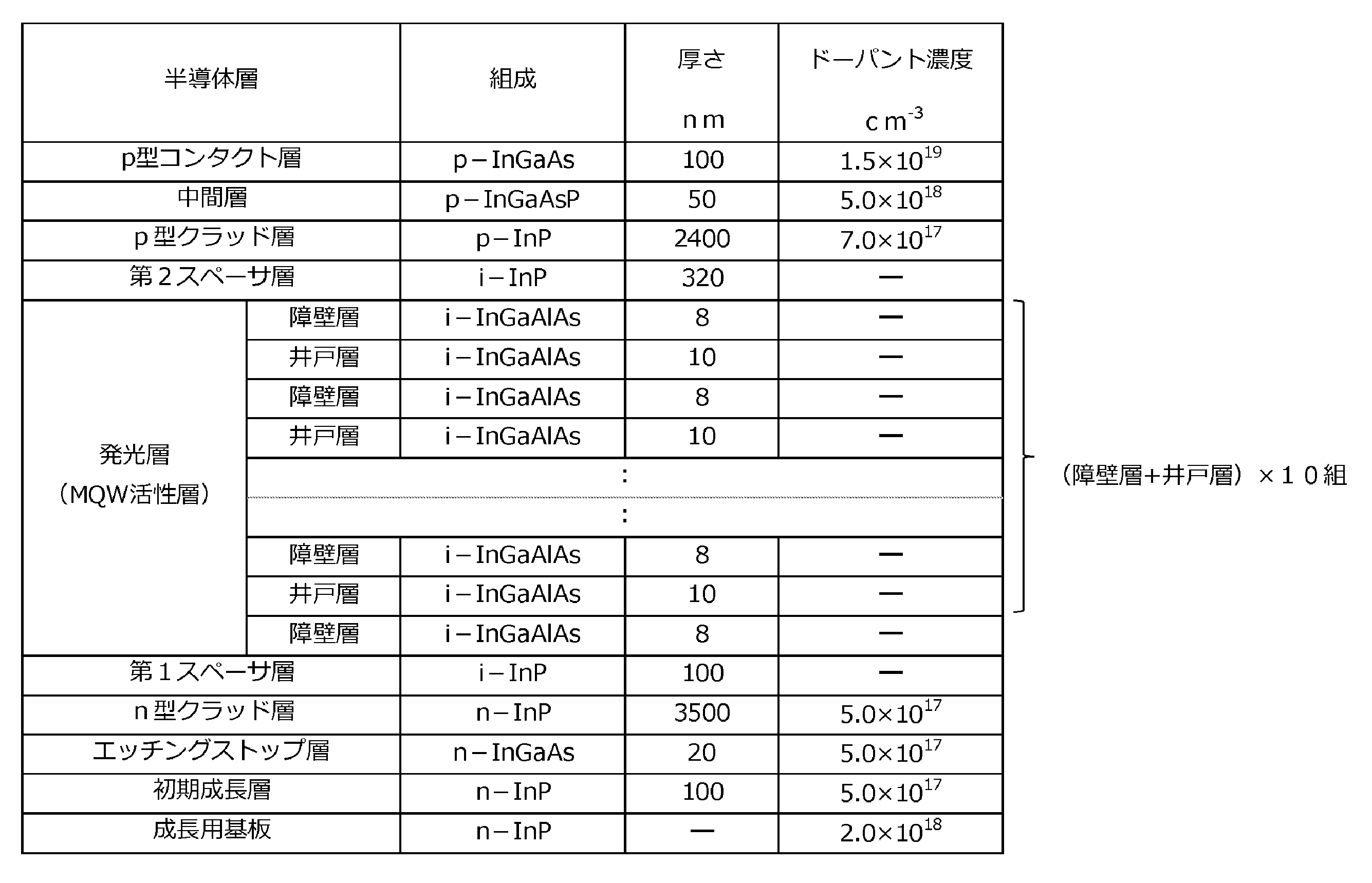
実施例1による半導体発光素子200のIII-V族化合物半導体層の各構成については図4の符号を参照し、後述の支持基板に接合する前の成長用基板の上に成長された状態について表2に厚さとドーパント濃度を示す。Sドープのn型InP基板を成長用基板10として用いた。n型InP基板(Sドープ、ドーパント濃度2.0×1018atoms/cm3)の(100)面上に、厚さ100nmのn型InP層及び厚さ20nmのn型In0.57Ga0.43As層(それぞれを初期成長層及びエッチングストップ層120)、厚さ3500nmのn型InP層(n型クラッド層としてのn型半導体層130)、厚さ100nmのi型InP層(第1スペーサ層141)、詳細を後述する発光層150、厚さ320nmのi型InP層(第2スペーサ層142)、厚さ2400nmのp型InP層(p型クラッド層171)、厚さ50nmのp型In0.8Ga0.2As0.5P0.5層(中間層172)、厚さ100nmのp型In0.57Ga0.43As層(p型コンタクト層173)をMOCVD法により順次形成した。n型InP層及びn型InGaAs層(それぞれを初期成長層及びエッチングストップ層120)、n型InP層(n型クラッド層としてのn型半導体層130)はSiドープを行い、ドーパント濃度は5.0×1017atoms/cm3とした。p型InP層(p型クラッド層171)はZnドープを行い、ドーパント濃度は7.0×1017atoms/cm3とした。p型InGaAsP層(中間層172)、p型InGaAs層(p型コンタクト層173)はZnドープを行い、ドーパント濃度は1.5×1019atoms/cm3とした。
障壁層となる第1層151の組成を、In0.5264Ga0.3597Al0.1139Asから、In0.5264Ga0.3166Al0.1570Asに変更した以外は、実施例1と同様にして実施例2にかかる半導体発光素子を得た。障壁層(第1層151)及び井戸層(第2層152)の、厚み、組成比、組成波長及び格子定数の値を、表3に記載する。実施例2の発光層の組成比における組成波長差は218.4nmであり、2つの格子定数の差の絶対値を2つの格子定数の平均値で割った値(格子定数差の比)は0.28%であり、伝導帯側の井戸深さ(Dc)の、伝導帯側の井戸深さ(Dc)と価電子帯の井戸深さ(Dv)の合計に対する比(Dc/(Dc+Dv))が68.7%であった。これらの値を表4に記載する。
障壁層(第1層151)の組成及び井戸層(第2層152)の組成と厚みを、表3に記載したとおりに変えた以外は、実施例1と同様にして、実施例3~5、及び比較例1~9にかかる半導体発光素子を得た。


半値幅
++・・・110nm未満
+・・・110nm以上120nm未満
-・・・120nm以上
発光出力
++・・・4.80mW以上
+・・・4.40mW以上4.80mW未満
-・・・4.40mW未満
20 介在層
30 n型半導体積層体
41 第1スペーサ層
42 第2スペーサ層
50 発光層
51 第1層
52 第2層
60 誘電体層
70 p型半導体層
71 p型クラッド層
72 中間層
73 p型コンタクト層
80 第2導電型電極
90 第1導電型電極
100 半導体発光素子
Claims (6)
- 第1のIII-V族化合物半導体層と第2のIII-V族化合物半導体層とを繰り返し積層した積層体を有する発光層を備える半導体発光素子であって、
前記第1及び前記第2のIII-V族化合物半導体層におけるIII族元素はAl、Ga、Inからなる群より選択される1種又は2種以上であり、
前記第1及び前記第2のIII-V族化合物半導体層におけるV族元素はAs、Sb、Pからなる群より選択される1種又は2種以上であり、
前記第1のIII-V族化合物半導体層の組成波長と、前記第2のIII-V族化合物半導体層の組成波長との組成波長差が70nm以上であり、
前記積層体のバンド構造における伝導帯側の井戸深さ(Dc)が、価電子帯側の井戸深さ(Dv)よりも大きく、かつ前記組成波長差により形成される前記伝導帯側の井戸深さ(Dc)の、前記伝導帯側の井戸深さ(Dc)と前記価電子帯の井戸深さ(Dv)の合計に対する比(Dc/(Dc+Dv))が65%以上であることを特徴とする、半導体発光素子。 - 前記第1のIII-V族化合物半導体層の格子定数と前記第2のIII-V族化合物半導体層の格子定数における、2つの格子定数の差の絶対値を2つの格子定数の平均値で割った値が、0.10%以上0.40%以下である、請求項1に記載の半導体発光素子。
- 前記価電子帯側の井戸深さ(Dv)が0.11eV以下である、請求項1に記載の半導体発光素子。
- 前記第1及び前記第2のIII-V族化合物半導体層におけるV族元素はAs、Sb、Pからなる群より選択される1種である、請求項1に記載の半導体発光素子。
- 前記第1のIII-V族化合物半導体層の組成波長と、前記第2のIII-V族化合物半導体層の組成波長との組成波長差が100nm以上290nm以下である、請求項1に記載の半導体発光素子。
- 請求項1~5のいずれか1項に記載の半導体発光素子を製造する方法であって、
前記発光層を形成する発光層形成工程を含み、
前記発光層形成工程は、前記第1のIII-V族化合物半導体層を形成する第1工程と、前記第2のIII-V族化合物半導体層を形成する第2工程と、を繰り返すことにより前記積層体を形成する、半導体発光素子の製造方法。
Priority Applications (3)
| Application Number | Priority Date | Filing Date | Title |
|---|---|---|---|
| US18/997,228 US20260006946A1 (en) | 2022-07-22 | 2023-07-19 | Semiconductor light-emitting element and method of producing semiconductor light-emitting element |
| DE112023003178.9T DE112023003178T5 (de) | 2022-07-22 | 2023-07-19 | Lichtemittierendes halbleiterelement und verfahren zur herstellung eines lichtemittierenden halbleiterelements |
| CN202380055067.2A CN119605044A (zh) | 2022-07-22 | 2023-07-19 | 半导体发光元件和半导体发光元件的制造方法 |
Applications Claiming Priority (4)
| Application Number | Priority Date | Filing Date | Title |
|---|---|---|---|
| JP2022-117526 | 2022-07-22 | ||
| JP2022117526 | 2022-07-22 | ||
| JP2023116899A JP7387048B1 (ja) | 2022-07-22 | 2023-07-18 | 半導体発光素子及び半導体発光素子の製造方法 |
| JP2023-116899 | 2023-07-18 |
Publications (1)
| Publication Number | Publication Date |
|---|---|
| WO2024019098A1 true WO2024019098A1 (ja) | 2024-01-25 |
Family
ID=88917931
Family Applications (1)
| Application Number | Title | Priority Date | Filing Date |
|---|---|---|---|
| PCT/JP2023/026476 Ceased WO2024019098A1 (ja) | 2022-07-22 | 2023-07-19 | 半導体発光素子及び半導体発光素子の製造方法 |
Country Status (6)
| Country | Link |
|---|---|
| US (1) | US20260006946A1 (ja) |
| JP (1) | JP7387048B1 (ja) |
| CN (1) | CN119605044A (ja) |
| DE (1) | DE112023003178T5 (ja) |
| TW (1) | TWI899596B (ja) |
| WO (1) | WO2024019098A1 (ja) |
Citations (4)
| Publication number | Priority date | Publication date | Assignee | Title |
|---|---|---|---|---|
| JP2002134842A (ja) * | 2000-10-26 | 2002-05-10 | Hitachi Ltd | 半導体レーザ装置 |
| WO2004112208A1 (ja) * | 2003-06-11 | 2004-12-23 | Nec Corporation | 半導体レーザ |
| JP2006196484A (ja) * | 2005-01-11 | 2006-07-27 | Hitachi Ltd | 光半導体装置 |
| WO2009100943A1 (de) * | 2008-02-15 | 2009-08-20 | Fraunhofer-Gesellschaft zur Förderung der angewandten Forschung e.V. | Infrarot-halbleiterlaser |
Family Cites Families (1)
| Publication number | Priority date | Publication date | Assignee | Title |
|---|---|---|---|---|
| KR101766719B1 (ko) * | 2010-03-25 | 2017-08-09 | 엘지이노텍 주식회사 | 발광 다이오드 및 이를 포함하는 발광 소자 패키지 |
-
2023
- 2023-07-18 JP JP2023116899A patent/JP7387048B1/ja active Active
- 2023-07-19 CN CN202380055067.2A patent/CN119605044A/zh active Pending
- 2023-07-19 WO PCT/JP2023/026476 patent/WO2024019098A1/ja not_active Ceased
- 2023-07-19 DE DE112023003178.9T patent/DE112023003178T5/de active Pending
- 2023-07-19 US US18/997,228 patent/US20260006946A1/en active Pending
- 2023-07-21 TW TW112127251A patent/TWI899596B/zh active
Patent Citations (4)
| Publication number | Priority date | Publication date | Assignee | Title |
|---|---|---|---|---|
| JP2002134842A (ja) * | 2000-10-26 | 2002-05-10 | Hitachi Ltd | 半導体レーザ装置 |
| WO2004112208A1 (ja) * | 2003-06-11 | 2004-12-23 | Nec Corporation | 半導体レーザ |
| JP2006196484A (ja) * | 2005-01-11 | 2006-07-27 | Hitachi Ltd | 光半導体装置 |
| WO2009100943A1 (de) * | 2008-02-15 | 2009-08-20 | Fraunhofer-Gesellschaft zur Förderung der angewandten Forschung e.V. | Infrarot-halbleiterlaser |
Also Published As
| Publication number | Publication date |
|---|---|
| TWI899596B (zh) | 2025-10-01 |
| JP2024014794A (ja) | 2024-02-01 |
| DE112023003178T5 (de) | 2025-05-22 |
| US20260006946A1 (en) | 2026-01-01 |
| CN119605044A (zh) | 2025-03-11 |
| JP7387048B1 (ja) | 2023-11-27 |
| TW202408030A (zh) | 2024-02-16 |
Similar Documents
| Publication | Publication Date | Title |
|---|---|---|
| JP5112511B2 (ja) | 放射線放出半導体ボディ | |
| US8648381B2 (en) | Semiconductor light emitting device | |
| US11201261B2 (en) | Deep ultraviolet light emitting element and method of manufacturing the same | |
| WO2018003374A1 (ja) | 半導体光デバイスの製造方法および半導体光デバイス | |
| CN101180743A (zh) | 氮化物半导体发光元件 | |
| JP2021129119A (ja) | 半導体光デバイスの製造方法及び半導体光デバイス | |
| CN113272974B (zh) | 半导体发光元件和半导体发光元件的制造方法 | |
| TWI803785B (zh) | 發光元件及其製造方法 | |
| US20120049155A1 (en) | Semiconductor light emitting device | |
| JP7387048B1 (ja) | 半導体発光素子及び半導体発光素子の製造方法 | |
| JP7413599B1 (ja) | Iii-v族化合物半導体発光素子及びiii-v族化合物半導体発光素子の製造方法 | |
| CN101651288A (zh) | 半导体器件 | |
| JP2022120619A (ja) | 発光素子 | |
| JP6158591B2 (ja) | 半導体レーザ | |
| TW202004854A (zh) | 半導體光元件的製造方法以及半導體光元件的中間體 |
Legal Events
| Date | Code | Title | Description |
|---|---|---|---|
| 121 | Ep: the epo has been informed by wipo that ep was designated in this application |
Ref document number: 23843021 Country of ref document: EP Kind code of ref document: A1 |
|
| WWE | Wipo information: entry into national phase |
Ref document number: 202380055067.2 Country of ref document: CN |
|
| WWE | Wipo information: entry into national phase |
Ref document number: 18997228 Country of ref document: US |
|
| WWE | Wipo information: entry into national phase |
Ref document number: 112023003178 Country of ref document: DE |
|
| WWP | Wipo information: published in national office |
Ref document number: 202380055067.2 Country of ref document: CN |
|
| WWP | Wipo information: published in national office |
Ref document number: 112023003178 Country of ref document: DE |
|
| 122 | Ep: pct application non-entry in european phase |
Ref document number: 23843021 Country of ref document: EP Kind code of ref document: A1 |
|
| WWP | Wipo information: published in national office |
Ref document number: 18997228 Country of ref document: US |