WO2024018741A1 - フィルムコンデンサ - Google Patents
フィルムコンデンサ Download PDFInfo
- Publication number
- WO2024018741A1 WO2024018741A1 PCT/JP2023/018562 JP2023018562W WO2024018741A1 WO 2024018741 A1 WO2024018741 A1 WO 2024018741A1 JP 2023018562 W JP2023018562 W JP 2023018562W WO 2024018741 A1 WO2024018741 A1 WO 2024018741A1
- Authority
- WO
- WIPO (PCT)
- Prior art keywords
- external electrode
- lead
- film
- terminal
- capacitor
- Prior art date
- Legal status (The legal status is an assumption and is not a legal conclusion. Google has not performed a legal analysis and makes no representation as to the accuracy of the status listed.)
- Ceased
Links
Images




Classifications
-
- H—ELECTRICITY
- H01—ELECTRIC ELEMENTS
- H01G—CAPACITORS; CAPACITORS, RECTIFIERS, DETECTORS, SWITCHING DEVICES, LIGHT-SENSITIVE OR TEMPERATURE-SENSITIVE DEVICES OF THE ELECTROLYTIC TYPE
- H01G4/00—Fixed capacitors; Processes of their manufacture
- H01G4/002—Details
- H01G4/228—Terminals
- H01G4/236—Terminals leading through the housing, i.e. lead-through
-
- H—ELECTRICITY
- H01—ELECTRIC ELEMENTS
- H01G—CAPACITORS; CAPACITORS, RECTIFIERS, DETECTORS, SWITCHING DEVICES, LIGHT-SENSITIVE OR TEMPERATURE-SENSITIVE DEVICES OF THE ELECTROLYTIC TYPE
- H01G4/00—Fixed capacitors; Processes of their manufacture
- H01G4/002—Details
- H01G4/005—Electrodes
- H01G4/015—Special provisions for self-healing
-
- H—ELECTRICITY
- H01—ELECTRIC ELEMENTS
- H01G—CAPACITORS; CAPACITORS, RECTIFIERS, DETECTORS, SWITCHING DEVICES, LIGHT-SENSITIVE OR TEMPERATURE-SENSITIVE DEVICES OF THE ELECTROLYTIC TYPE
- H01G4/00—Fixed capacitors; Processes of their manufacture
- H01G4/002—Details
- H01G4/018—Dielectrics
- H01G4/06—Solid dielectrics
- H01G4/14—Organic dielectrics
- H01G4/18—Organic dielectrics of synthetic material, e.g. derivatives of cellulose
-
- H—ELECTRICITY
- H01—ELECTRIC ELEMENTS
- H01G—CAPACITORS; CAPACITORS, RECTIFIERS, DETECTORS, SWITCHING DEVICES, LIGHT-SENSITIVE OR TEMPERATURE-SENSITIVE DEVICES OF THE ELECTROLYTIC TYPE
- H01G4/00—Fixed capacitors; Processes of their manufacture
- H01G4/002—Details
- H01G4/228—Terminals
-
- H—ELECTRICITY
- H01—ELECTRIC ELEMENTS
- H01G—CAPACITORS; CAPACITORS, RECTIFIERS, DETECTORS, SWITCHING DEVICES, LIGHT-SENSITIVE OR TEMPERATURE-SENSITIVE DEVICES OF THE ELECTROLYTIC TYPE
- H01G4/00—Fixed capacitors; Processes of their manufacture
- H01G4/002—Details
- H01G4/228—Terminals
- H01G4/232—Terminals electrically connecting two or more layers of a stacked or rolled capacitor
-
- H—ELECTRICITY
- H01—ELECTRIC ELEMENTS
- H01G—CAPACITORS; CAPACITORS, RECTIFIERS, DETECTORS, SWITCHING DEVICES, LIGHT-SENSITIVE OR TEMPERATURE-SENSITIVE DEVICES OF THE ELECTROLYTIC TYPE
- H01G4/00—Fixed capacitors; Processes of their manufacture
- H01G4/32—Wound capacitors
-
- H—ELECTRICITY
- H01—ELECTRIC ELEMENTS
- H01G—CAPACITORS; CAPACITORS, RECTIFIERS, DETECTORS, SWITCHING DEVICES, LIGHT-SENSITIVE OR TEMPERATURE-SENSITIVE DEVICES OF THE ELECTROLYTIC TYPE
- H01G4/00—Fixed capacitors; Processes of their manufacture
- H01G4/002—Details
- H01G4/224—Housing; Encapsulation
Definitions
- the present invention relates to a film capacitor.
- a film capacitor As a type of capacitor, a film capacitor is known in which a flexible resin film is used as a dielectric film, and metal layers are arranged facing each other with the dielectric film in between.
- a capacitor element constituting a film capacitor is produced, for example, by manufacturing a laminate in which a metalized film, in which a metal layer is provided on the surface of a dielectric film, is wound or laminated, and then external electrodes are attached to both end faces of the laminate. (also called metallicon electrodes).
- a lead wire or a lead terminal such as a bus bar is connected to the external electrode of the capacitor element.
- Examples of the connection method of the lead terminal include a method of joining the lead terminal to the external electrode of the capacitor element by soldering or resistance welding.
- Patent Document 1 includes a capacitor element formed by winding or laminating a metallized film and having a metallicon electrode, and a metal bar that is soldered to the metallicon electrode, and the metal bar has a convex portion for solder connection.
- a metallized film capacitor is disclosed.
- the lead electrode connected to the capacitor element is made of a metal bar having a cross-sectional area necessary for the circuit, so that a large current can flow through it, and the metal bar is provided with a protrusion for solder connection.
- Patent Document 2 describes a capacitor element and a metallicon electrode formed by thermally spraying molten metal such as lead or tin on both end faces of the capacitor element, and a metallicon electrode that is connected and fixed to the metallicon electrode with an electric welding machine or the like, while the other A film capacitor configured with lead wires is disclosed.
- the film capacitor described in Patent Document 2 is characterized in that one of the metallcone joint surfaces of the lead wire is formed in a series in the vertical direction in a substantially mountain shape or a substantially sawtooth shape.
- Patent Document 2 in a method of joining an extraction terminal such as a lead wire to an external electrode of a capacitor element by resistance welding, the external electrode and the extraction terminal are pressed against each other by a welding electrode. The lead terminal is welded to the external electrode by flowing a large current from the welding electrode.
- An object of the present invention is to provide a film capacitor with high bonding strength between the external electrode of the capacitor element and the lead terminal.
- the film capacitor of the present invention includes a capacitor element including an element body, an external electrode provided on an end surface of the element body, and a lead terminal electrically connected to the external electrode.
- the element body is a laminate including a metallized film in which a metal layer is provided on at least one main surface of a dielectric film.
- the external electrode is connected to the metal layer.
- the lead terminal is welded to the external electrode.
- the surface roughness Ra of the external electrode is 20 ⁇ m or more and 45 ⁇ m or less, and the digging depth of the lead terminal from the surface of the external electrode is 0.5 mm or more.
- FIG. 1 is a perspective view schematically showing a film capacitor according to an embodiment of the present invention.
- FIG. 2 is a front view of the film capacitor shown in FIG. 1.
- FIG. 3A is a side view schematically showing an example of an external electrode and a lead-out terminal before welding
- FIG. 3B is a side view schematically showing an example of an external electrode and a lead-out terminal after welding.
- FIG. 4A is a front view schematically showing an example of an external electrode and a lead-out terminal before welding
- FIG. 4B is a front view schematically showing an example of an external electrode and a lead-out terminal after welding.
- FIG. 5 is a front view schematically showing an example of a lead-out terminal that has cut into an external electrode.
- FIG. 1 is a perspective view schematically showing a film capacitor according to an embodiment of the present invention.
- FIG. 2 is a front view of the film capacitor shown in FIG. 1.
- FIG. 3A is a side view schematically showing an example of an
- FIG. 6 is a front view schematically showing another example of a lead-out terminal that has cut into an external electrode.
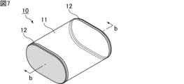
- FIG. 7 is a perspective view schematically showing an example of a capacitor element constituting the film capacitor of the present invention.
- FIG. 8 is a sectional view taken along line bb of the capacitor element shown in FIG.
- FIG. 9 is a perspective view schematically showing an example of an element main body constituting the capacitor element shown in FIGS. 7 and 8.
- FIG. 10 is a perspective view schematically showing another example of an element main body constituting the capacitor element shown in FIGS. 7 and 8.
- FIG. 11A and 11B are perspective views schematically showing an example of how the film capacitor shown in FIG. 1 is used.
- FIG. 12 is a schematic diagram for explaining a tensile test.
- the present invention is not limited to the following configuration, and may be modified as appropriate without changing the gist of the present invention. Furthermore, the present invention also includes a combination of a plurality of individual preferred configurations described below.
- FIG. 1 is a perspective view schematically showing a film capacitor according to an embodiment of the present invention.
- FIG. 2 is a front view of the film capacitor shown in FIG. 1.
- the film capacitor 1 shown in FIGS. 1 and 2 includes a capacitor element 10 and a lead terminal 20.
- the capacitor element 10 includes an element body 11 and an external electrode 12 provided on the end surface of the element body 11. Specifically, a pair of external electrodes 12 are provided on both end surfaces of the element body 11. The configuration of capacitor element 10 will be described later.
- the lead terminal 20 is electrically connected to the external electrode 12. Specifically, a pair of lead terminals 20 are electrically connected to each of the pair of external electrodes 12 .
- the pair of lead terminals 20 may extend from the external electrode 12 such that the distance between them is large.
- the pair of lead terminals 20 may extend from the external electrode 12 such that the distance between them is constant.
- the lead terminal 20 is welded to the external electrode 12. Specifically, the lead terminal 20 is resistance welded to the external electrode 12.
- the welded portion of the pull-out terminal 20 may be flat.
- the extraction terminal 20 is a lead wire.
- the lead wire may or may not have a plating layer on its surface.
- the welded portion of the lead wire may be processed into a flat plate shape.
- the extraction terminal 20 is a bus bar.
- the bus bar has a flat plate shape as a whole including the welded portion.
- FIG. 3A is a side view schematically showing an example of an external electrode and a lead-out terminal before welding
- FIG. 3B is a side view schematically showing an example of an external electrode and a lead-out terminal after welding
- FIG. 4A is a front view schematically showing an example of an external electrode and a lead-out terminal before welding
- FIG. 4B is a front view schematically showing an example of an external electrode and a lead-out terminal after welding.
- a large current is applied from the welding electrode 80 while the external electrode 12 and the extraction terminal 20 are pressed against each other by the welding electrode 80.
- the large current generates heat at the interface between the external electrode 12 and the lead terminal 20, causing the external electrode 12 to soften.
- the lead terminal 20 bites into the external electrode 12, as shown in FIGS. 3B and 4B.
- FIG. 5 is a front view schematically showing an example of a lead-out terminal that has cut into an external electrode.
- the lead-out terminal 20 that has bitten into the external electrode 12 becomes difficult to detach from the external electrode 12 because the external electrode 12 receives the acting force shown by the arrow in FIG.
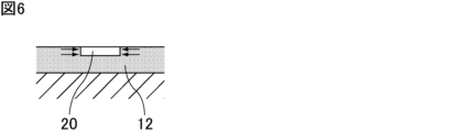
- FIG. 6 is a front view schematically showing another example of a lead-out terminal that bites into an external electrode.
- the entire extraction terminal 20 may bite into the external electrode 12.
- the film capacitor of the present invention is characterized in that the depth of penetration of the lead terminal from the surface of the external electrode (the length indicated by D in FIGS. 3B and 4B) is 0.5 mm or more.
- the depth of penetration of the lead terminal can be easily controlled by the amount of displacement of the welding machine. Therefore, it is possible to manufacture film capacitors of stable quality.
- the bonding strength between the external electrode and the lead terminal can be controlled by the depth of penetration of the lead terminal. Therefore, sufficient bonding strength can be ensured without alloying the lead terminal (for example, a plating layer provided on the surface of the lead wire) and the external electrode by welding.
- the lead terminal and the external electrode may or may not be alloyed.
- the depth of penetration of the lead terminal from the surface of the external electrode can be measured, for example, by measuring the weld location using 3D measurement with a digital microscope on a sample after weld strength measurement.
- the depth of penetration of the lead terminal from the surface of the external electrode is 0.7 mm or more.
- the extraction terminal can penetrate up to the thickness of the external electrode. Therefore, the depth of penetration of the lead terminal from the surface of the external electrode is equal to or less than the thickness of the external electrode.
- the lead terminal can only dig into the external electrode up to the thickness of the welded part. Therefore, it is preferable that the depth of penetration of the lead terminal from the surface of the external electrode is equal to or less than the thickness of the welded portion of the lead terminal.
- the thickness of the welded portion of the lead terminal is preferably 0.5 mm or more.
- the thickness of the welded portion of the lead terminal is more preferably 0.7 mm or more. Note that there is no particular upper limit to the thickness of the welded portion of the lead-out terminal.
- the film capacitor of the present invention is characterized in that the surface roughness Ra of the external electrode is 20 ⁇ m or more and 45 ⁇ m or less.
- the lead terminal can be inserted into the external electrode in a short time without damaging the capacitor element.
- the surface roughness Ra of the external electrode can be determined, for example, by measuring the surface roughness of the external electrode at two locations at both ends and at the center using a laser microscope (manufactured by Keyence Corporation, VK-8700), and then determining the average of the measurements. The value can be taken as the value of surface roughness Ra.
- the element body constituting the capacitor element is a laminate including a metallized film in which a metal layer is provided on at least one main surface of a dielectric film, and the external electrode constituting the capacitor element is , connected to the metal layer.
- the laminate has, for example, a columnar shape with an elliptical cross section, and external electrodes formed by, for example, metal spraying (metallicon) are provided on both end faces in the direction of the central axis.
- the above-mentioned laminate may be a rolled body in which metalized films are laminated and wound.
- a wound type film capacitor in which metalized films are laminated and wound will be described, but a laminated type film capacitor in which metalized films are laminated may also be used.
- FIG. 7 is a perspective view schematically showing an example of a capacitor element constituting the film capacitor of the present invention.
- FIG. 8 is a sectional view taken along line bb of the capacitor element shown in FIG.
- the element body 11 is a laminate including a first metallized film 51 and a second metallized film 52.
- the element main body 11 is a wound body in which a first metallized film 51 and a second metallized film 52 are laminated and wound.
- a pair of external electrodes 12 are electrically connected to both end surfaces of the element body 11 .
- the first metallized film 51 includes a first dielectric film 53 and a first metal layer 55 provided on the surface of the first dielectric film 53.
- the metallized film 52 includes a second dielectric film 54 and a second metal layer 56 provided on the surface of the second dielectric film 54.
- the first metal layer 55 and the second metal layer 56 face each other with the first dielectric film 53 or the second dielectric film 54 in between. Furthermore, the first metal layer 55 is electrically connected to one external electrode 12 , and the second metal layer 56 is electrically connected to the other external electrode 12 .
- the first dielectric film 53 and the second dielectric film 54 may have different configurations, but preferably have the same configuration.
- the first metal layer 55 is formed on one surface of the first dielectric film 53 so that it reaches one side edge but does not reach the other side edge.
- the second metal layer 56 is formed on one surface of the second dielectric film 54 so that it does not reach one side edge but reaches the other side edge.
- the first metal layer 55 and the second metal layer 56 are made of, for example, an aluminum layer.
- FIG. 9 is a perspective view schematically showing an example of an element main body that constitutes the capacitor element shown in FIGS. 7 and 8.
- the end of the first metal layer 55 reaching the side edge of the first dielectric film 53 and the second dielectric layer of the second metal layer 56 The first dielectric film 53 and the second dielectric film 54 are aligned with each other in the width direction (see FIG. (in the left-right direction), they are stacked.
- the element main body 11 becomes a rolled body of metallized film by winding the first dielectric film 53 and the second dielectric film 54 in a laminated state.
- the metal layer 55 and the second metal layer 56 are stacked with their ends exposed.
- the second dielectric film 54 is placed outside the first dielectric film 53, and for each of the first dielectric film 53 and the second dielectric film 54, Each of the first metal layer 55 and the second metal layer 56 is wound so as to face inward.
- FIG. 10 is a perspective view schematically showing another example of the element main body constituting the capacitor element shown in FIGS. 7 and 8.
- the cross-sectional shape is pressed into a flat shape such as an ellipse or an ellipse, and the cross-sectional shape is a perfect circle, as shown in FIG. It is preferable to have a more compact shape. In this case, the entire film capacitor can be downsized.
- the rolled body of metallized film may be provided with a cylindrical winding shaft.
- the winding shaft is arranged on the central axis of the metallized film in a wound state, and serves as the winding shaft when winding the metallized film.
- the external electrodes 12 are formed by spraying, for example, zinc or the like onto each end surface of the element body 11 obtained as described above.
- One external electrode 12 contacts the exposed end of the first metal layer 55 and is thereby electrically connected to the first metal layer 55 .
- the other external electrode 12 contacts the exposed end of the second metal layer 56 and is thereby electrically connected to the second metal layer 56 .
- the dielectric film constituting the element body of the capacitor element may contain a curable resin as a main component, or may contain a thermoplastic resin as a main component. From the viewpoint of improving the heat resistance of the film capacitor, the dielectric film preferably contains a curable resin as a main component.
- the main component of the dielectric film means the component with the largest weight percentage, preferably a component with a weight percentage of more than 50% by weight. Therefore, the dielectric film may include, as components other than the main component, additives such as silicone resin, and uncured portions of starting materials such as the first organic material and second organic material described below.
- the curable resin may be a thermosetting resin or a photocurable resin.
- thermosetting resin means a resin that can be cured by heat, and does not limit the curing method. Therefore, as long as the resin can be cured by heat, resins cured by methods other than heat (eg, light, electron beam, etc.) are also included in thermosetting resins. Furthermore, depending on the material, a reaction may start due to the reactivity of the material itself, and those that harden without necessarily applying heat or light from the outside are also considered thermosetting resins. The same applies to photocurable resins, and the curing method is not limited.
- the curable resin may or may not have at least one of a urethane bond and a urea bond.
- resins include urethane resins having urethane bonds, urea resins having urea bonds, and the like. Further, a resin having both urethane bonds and urea bonds may be used.
- urethane bonds and/or urea bonds can be confirmed using a Fourier transform infrared spectrophotometer (FT-IR).
- FT-IR Fourier transform infrared spectrophotometer
- the curable resin is preferably made of a cured product of a first organic material and a second organic material.
- a cured product obtained by a reaction between a hydroxyl group (OH group) of the first organic material and an isocyanate group (NCO group) of the second organic material can be mentioned.
- the dielectric film may include at least one of an isocyanate group and a hydroxyl group.
- the dielectric film may contain either an isocyanate group or a hydroxyl group, or may contain both an isocyanate group and a hydroxyl group.
- FT-IR Fourier transform infrared spectrophotometer
- the first organic material is preferably a polyol having multiple hydroxyl groups in the molecule.
- the polyol include polyether polyol, polyester polyol, polyvinyl acetal, and the like.
- the first organic material two or more types of organic materials may be used in combination.
- the second organic material is preferably an isocyanate compound, an epoxy resin, or a melamine resin that has multiple functional groups in its molecule.
- the second organic material two or more types of organic materials may be used in combination. Among the second organic materials, isocyanate compounds are preferred.
- isocyanate compound examples include aromatic polyisocyanates such as diphenylmethane diisocyanate (MDI) and tolylene diisocyanate (TDI), and aliphatic polyisocyanates such as hexamethylene diisocyanate (HDI). Modified products of these polyisocyanates, for example, modified products having carbodiimide or urethane, etc., may also be used.
- aromatic polyisocyanates such as diphenylmethane diisocyanate (MDI) and tolylene diisocyanate (TDI)
- aliphatic polyisocyanates such as hexamethylene diisocyanate (HDI).
- Modified products of these polyisocyanates for example, modified products having carbodiimide or urethane, etc., may also be used.
- the epoxy resin is not particularly limited as long as it has an epoxy ring, and examples thereof include bisphenol A epoxy resin, biphenyl skeleton epoxy resin, cyclopentadiene skeleton epoxy resin, naphthalene skeleton epoxy resin, and the like.
- the melamine resin is not particularly limited as long as it is an organic nitrogen compound having a triazine ring at the center of its structure and three amino groups around it, and examples include alkylated melamine resins. In addition, modified forms of melamine may also be used.
- the dielectric film constituting the element body of the capacitor element is preferably formed by forming a resin solution containing a first organic material and a second organic material into a film shape, and then hardening by heat treatment.
- the dielectric film constituting the element body of the capacitor element may contain a vapor-deposited polymer film as a main component.
- the vapor-deposited polymer film may or may not have at least one of a urethane bond and a urea bond.
- the vapor-deposited polymer film refers to a film formed by a vapor-deposition polymerization method, and is basically included in curable resins.
- the dielectric film constituting the element body of the capacitor element may contain thermoplastic resin as a main component.
- thermoplastic resin include polypropylene, polyether sulfone, polyetherimide, polyarylate, and the like.
- the dielectric film constituting the element body of the capacitor element can also contain additives for adding other functions.
- smoothness can be imparted by adding a leveling agent.
- the additive has a functional group that reacts with a hydroxyl group and/or an isocyanate group, and is a material that forms a part of the crosslinked structure of the cured product. Examples of such materials include resins having at least one functional group selected from the group consisting of epoxy groups, silanol groups, and carboxyl groups.
- the thickness of the dielectric film constituting the element body of the capacitor element is not particularly limited, but may be set as appropriate depending on the required capacitance and the required element volume of the capacitor to be manufactured. .
- the thickness of the dielectric film can be measured using an optical film thickness meter.
- the type of metal contained in the metal layer constituting the element body of the capacitor element is not particularly limited. It is preferable that the material contains one selected from the group consisting of Mg), tin (Sn), and nickel (Ni).
- the thickness of the metal layer constituting the element body of the capacitor element is not particularly limited, but from the viewpoint of suppressing damage to the metal layer, the thickness of the metal layer is 5 nm or more and 40 nm or less. It is preferable.
- the thickness of the metal layer can be determined by observing a cross section of the metallized film cut in the thickness direction using an electron microscope such as a field emission scanning electron microscope (FE-SEM).
- FE-SEM field emission scanning electron microscope
- FIG. 11A and 11B are perspective views schematically showing an example of how to use the film capacitor shown in FIG. 1.
- the film capacitor 1 is housed in the outer case 30.
- the exterior case 30 may be a resin case or a metal case.
- a rectangular parallelepiped space is formed inside the exterior case 30.
- the capacitor element 10 be disposed in the center of the interior of the exterior case 30 while being separated from the inner surface of the exterior case 30.
- the exterior case 30 has, for example, a bottomed cylindrical shape with an opening 31 at one end.
- the exterior case 30 includes a bottom wall 32 that faces the opening 31 and seals the other end, and a side wall 33 that projects from the bottom wall 32 toward the opening 31.
- the exterior case 30 has a substantially rectangular opening 31 at one end, a bottom wall 32 facing the opening 31 and sealing the other end, and a bottom wall 32 extending from the bottom wall 32 toward the opening 31. It has a square cylindrical shape with a bottom and a square cylindrical side wall 33 that protrudes. Note that the outer case 30 may have a shape such as a bottomed tube including a cylindrical side wall 33 instead of the square tube-shaped side wall 33.
- the side wall 33 of the exterior case 30 is provided with a recess 33a on the side on the opening 31 side.
- the recess 33a in the opening surface of the exterior case 30, when the film capacitor is mounted on the board, it is possible to prevent the film capacitor and the board from being sealed together and internal pressure from increasing. Note that the exterior case 30 does not need to be provided with the recess 33a.
- a guide groove for regulating the position of the pull-out terminal 20 may be provided on the inner surface of the exterior case 30.
- the pull-out terminal 20 protrudes from the inside of the exterior case 30 toward the outside. As shown in FIG. 11B, it is preferable that the distance between the pair of lead-out terminals 20 is constant.
- a resin can be appropriately selected according to the required function.
- the filling resin 40 include epoxy resin, silicone resin, and urethane resin.
- a curing agent for the epoxy resin an amine curing agent, an imidazole curing agent, etc. may be used.
- the filling resin 40 only resin may be used, but a reinforcing agent may be added for the purpose of improving the strength.
- reinforcing agents include inorganic fillers such as silica and alumina, organic fillers such as polyethylene fibers and polyamide fibers, and organic-inorganic composite fillers in which the surface of inorganic powder is coated with an organic material such as a silane coupling agent. etc. are used.
- the relationship between the height of the filled resin 40 and the height of the exterior case 30 is such that the resin in the opening 31 of the exterior case 30 is made as thick as possible, and may be as thick as possible up to the inside of the exterior case 30, or may be as thick as possible. It may be slightly overflowing due to surface tension.
- the lead terminal is welded to the external electrode, the surface roughness Ra of the external electrode is 20 ⁇ m or more and 45 ⁇ m or less, and the depth of penetration of the lead terminal from the surface of the external electrode is 0.5 mm or more.
- the present invention is not limited to the above embodiments. Therefore, various applications and modifications can be made within the scope of the present invention regarding the structure, manufacturing conditions, etc. of the film capacitor.
- the film capacitor of the present invention when a pair of external electrodes are provided on both end faces of the element body and a pair of lead terminals are electrically connected to each of the pair of external electrodes, at least one external electrode It is only necessary that the lead terminal and the lead terminal electrically connected to the external electrode satisfy the relationship described in the above embodiment.
- FIG. 11A and 11B show an example in which a single capacitor element is housed inside a single exterior case.
- a plurality of capacitor elements may be housed inside the exterior case.
- the portion where the lead terminal such as a lead wire is electrically connected to the external electrode of the capacitor element is provided in a small area of the external electrode, so when a load is applied to the lead terminal, There is a risk that the lead terminal may separate from the electrode. Therefore, in the interior of the exterior case, it is preferable that the filling resin be located outside the external electrode of the capacitor element and the lead-out terminal to tightly fix the two. Thereby, even if a load is applied to the protruding portion of the lead-out terminal, the connection between the lead-out terminal and the external electrode is reinforced by the filled resin, and separation of the two can be suppressed.
- connection position between the external electrode and the lead terminal is not particularly limited, and may be, for example, at the center of the external electrode as shown in FIG. 1, or as described in FIG. 1 of Patent No. 4733566. It may be on the case opening side or on the case bottom side.
- a capacitor element including an element body and an external electrode provided on an end surface of the element body; A lead-out terminal electrically connected to the external electrode,
- the element body is a laminate including a metallized film in which a metal layer is provided on at least one main surface of a dielectric film, the external electrode is connected to the metal layer, The extraction terminal is welded to the external electrode,
- the surface roughness Ra of the external electrode is 20 ⁇ m or more and 45 ⁇ m or less,
- a film capacitor, wherein the lead terminal has a digging depth of 0.5 mm or more from the surface of the external electrode.
- ⁇ 3> The film capacitor according to ⁇ 1> or ⁇ 2>, wherein the depth of penetration of the lead terminal from the surface of the external electrode is equal to or less than the thickness of the welded portion of the lead terminal.
- ⁇ 4> The film capacitor according to any one of ⁇ 1> to ⁇ 3>, wherein the welded portion of the lead-out terminal has a thickness of 0.5 mm or more.
- ⁇ 5> The film capacitor according to any one of ⁇ 1> to ⁇ 4>, wherein the welded portion of the lead-out terminal has a flat plate shape.
- ⁇ 6> The film capacitor according to any one of ⁇ 1> to ⁇ 5>, wherein the extraction terminal is a lead wire.
- ⁇ 7> The film capacitor according to any one of ⁇ 1> to ⁇ 6>, wherein the laminate is a wound body in which the metallized films are laminated and wound.
- a film capacitor having a configuration similar to that shown in FIG. 1 was prepared.
- a lead wire with an outer diameter of 1.2 mm was used as the extraction terminal.
- the welded portion of the lead wire was processed into a flat plate with a thickness of 0.75 mm.
- the surface roughness Ra of the external electrode was adjusted to fall within the range of 20 ⁇ m to 45 ⁇ m.
- the depth of penetration of the lead wire which is the extraction terminal, was varied in the range of 0.2 mm to 0.75 mm.
- the bonding strength between the external electrode and the lead-out terminal was evaluated by the following tensile test.
- FIG. 12 is a schematic diagram for explaining the tensile test.
- the capacitor element 10 to which the lead terminal 20 is connected is fixed, and the lead terminal 20 is bent in the direction of the winding axis (direction indicated by the arrow in FIG. 12). The strength was measured.
- the temperature at which the dimensional change rate measured by thermomechanical analysis (TMA) reaches 5% is 300°C or less in both cases. Met.
- the temperature at which the dimensional change rate measured by TMA reached 5% was 383° C. From these results, if the surface roughness Ra of the external electrode is 20 ⁇ m or more and 45 ⁇ m or less, welding can be performed at a temperature of 300°C or less, so the lead terminal can be connected in a short time without damaging the capacitor element. It is thought that it can be made to bite into the external electrode.
- the dimensional change rate of the external electrode is calculated as follows. ⁇ TMA measurement mode> Needle insertion mode ⁇ TMA measurement method: Calculation of dimensional change rate> Cut the external electrode to a predetermined size and use it as a sample.
- the size of the sample may be approximately 5 mm x 5 mm.
- An indenter is placed at the center of the surface of the sample, and the sample is heated to 450° C. at a heating rate of 10° C./min while applying a load of 100 gf to the indenter.
- the penetration depth of the indenter is measured from the start of measurement until the indenter is heated to 450°C. This penetration depth is divided by the thickness of the sample and multiplied by 100.
- This operation is also performed on four samples in which other parts of the external electrodes are cut out.
- the average value of the five values obtained is defined as the dimensional change rate of the external electrode.
- the temperature at which the dimensional change rate of the external electrode becomes 5% is measured by heating to 450°C. This means that the temperatures (temperatures measured) were all below 300°C.
Landscapes
- Engineering & Computer Science (AREA)
- Power Engineering (AREA)
- Manufacturing & Machinery (AREA)
- Microelectronics & Electronic Packaging (AREA)
- Fixed Capacitors And Capacitor Manufacturing Machines (AREA)
Priority Applications (3)
| Application Number | Priority Date | Filing Date | Title |
|---|---|---|---|
| JP2024534945A JP7829038B2 (ja) | 2022-07-22 | 2023-05-18 | フィルムコンデンサ |
| CN202380054261.9A CN119631150A (zh) | 2022-07-22 | 2023-05-18 | 薄膜电容器 |
| US19/032,667 US20250166919A1 (en) | 2022-07-22 | 2025-01-21 | Film capacitor |
Applications Claiming Priority (2)
| Application Number | Priority Date | Filing Date | Title |
|---|---|---|---|
| JP2022117415 | 2022-07-22 | ||
| JP2022-117415 | 2022-07-22 |
Related Child Applications (1)
| Application Number | Title | Priority Date | Filing Date |
|---|---|---|---|
| US19/032,667 Continuation US20250166919A1 (en) | 2022-07-22 | 2025-01-21 | Film capacitor |
Publications (1)
| Publication Number | Publication Date |
|---|---|
| WO2024018741A1 true WO2024018741A1 (ja) | 2024-01-25 |
Family
ID=89617363
Family Applications (1)
| Application Number | Title | Priority Date | Filing Date |
|---|---|---|---|
| PCT/JP2023/018562 Ceased WO2024018741A1 (ja) | 2022-07-22 | 2023-05-18 | フィルムコンデンサ |
Country Status (4)
| Country | Link |
|---|---|
| US (1) | US20250166919A1 (https=) |
| JP (1) | JP7829038B2 (https=) |
| CN (1) | CN119631150A (https=) |
| WO (1) | WO2024018741A1 (https=) |
Cited By (1)
| Publication number | Priority date | Publication date | Assignee | Title |
|---|---|---|---|---|
| CN119419065A (zh) * | 2024-10-22 | 2025-02-11 | 甬江实验室 | 薄膜电容、电容组件以及电容组件制备方法 |
Citations (3)
| Publication number | Priority date | Publication date | Assignee | Title |
|---|---|---|---|---|
| JPS5232570A (en) * | 1975-09-05 | 1977-03-11 | Shizuki Electric | Method of fixing lead wires to capacitor |
| JPH01287913A (ja) * | 1988-05-13 | 1989-11-20 | Nichicon Corp | チップ形フイルムコンデンサの製造方法 |
| JP2016082128A (ja) * | 2014-10-20 | 2016-05-16 | ニチコン株式会社 | 金属化フィルムコンデンサにおけるバスバー溶接構造 |
-
2023
- 2023-05-18 WO PCT/JP2023/018562 patent/WO2024018741A1/ja not_active Ceased
- 2023-05-18 JP JP2024534945A patent/JP7829038B2/ja active Active
- 2023-05-18 CN CN202380054261.9A patent/CN119631150A/zh active Pending
-
2025
- 2025-01-21 US US19/032,667 patent/US20250166919A1/en active Pending
Patent Citations (3)
| Publication number | Priority date | Publication date | Assignee | Title |
|---|---|---|---|---|
| JPS5232570A (en) * | 1975-09-05 | 1977-03-11 | Shizuki Electric | Method of fixing lead wires to capacitor |
| JPH01287913A (ja) * | 1988-05-13 | 1989-11-20 | Nichicon Corp | チップ形フイルムコンデンサの製造方法 |
| JP2016082128A (ja) * | 2014-10-20 | 2016-05-16 | ニチコン株式会社 | 金属化フィルムコンデンサにおけるバスバー溶接構造 |
Cited By (1)
| Publication number | Priority date | Publication date | Assignee | Title |
|---|---|---|---|---|
| CN119419065A (zh) * | 2024-10-22 | 2025-02-11 | 甬江实验室 | 薄膜电容、电容组件以及电容组件制备方法 |
Also Published As
| Publication number | Publication date |
|---|---|
| JP7829038B2 (ja) | 2026-03-12 |
| CN119631150A (zh) | 2025-03-14 |
| JPWO2024018741A1 (https=) | 2024-01-25 |
| US20250166919A1 (en) | 2025-05-22 |
Similar Documents
| Publication | Publication Date | Title |
|---|---|---|
| JP7057923B2 (ja) | フィルムコンデンサ、及び、フィルムコンデンサ用の外装ケース | |
| WO2024018741A1 (ja) | フィルムコンデンサ | |
| KR20200001488A (ko) | 적층 세라믹 전자 부품 | |
| US20190287710A1 (en) | Coil component and manufacturing method for same | |
| US10366830B2 (en) | Surface mount electronic component | |
| JP6538909B2 (ja) | 電流検出器 | |
| WO2025047126A1 (ja) | コンデンサモジュール | |
| US11923147B2 (en) | Film capacitor | |
| JP7839292B2 (ja) | コンデンサ | |
| JP7244032B2 (ja) | フィルムコンデンサ | |
| JP7668367B2 (ja) | コンデンサ | |
| JP7428493B2 (ja) | フィルムコンデンサ | |
| US20250157736A1 (en) | Capacitor | |
| US12586725B2 (en) | Capacitor having an external electrode with increased porosity | |
| JP2026051853A (ja) | コンデンサモジュール | |
| US12406812B2 (en) | Film capacitor | |
| JP2026068220A (ja) | コンデンサモジュール | |
| JP2026068221A (ja) | コンデンサモジュール | |
| JP7698692B2 (ja) | コンデンサ | |
| US12176155B2 (en) | Tantalum capacitor having lead frame including plural electrode portions inclined in different directions | |
| JP2026068219A (ja) | コンデンサモジュール | |
| WO2025032938A1 (ja) | フィルムコンデンサ | |
| JP2026068218A (ja) | コンデンサモジュール | |
| WO2025203986A1 (ja) | フィルムコンデンサ | |
| WO2024079967A1 (ja) | コンデンサ |
Legal Events
| Date | Code | Title | Description |
|---|---|---|---|
| 121 | Ep: the epo has been informed by wipo that ep was designated in this application |
Ref document number: 23842673 Country of ref document: EP Kind code of ref document: A1 |
|
| WWE | Wipo information: entry into national phase |
Ref document number: 2024534945 Country of ref document: JP |
|
| WWE | Wipo information: entry into national phase |
Ref document number: 202380054261.9 Country of ref document: CN |
|
| NENP | Non-entry into the national phase |
Ref country code: DE |
|
| WWP | Wipo information: published in national office |
Ref document number: 202380054261.9 Country of ref document: CN |
|
| 122 | Ep: pct application non-entry in european phase |
Ref document number: 23842673 Country of ref document: EP Kind code of ref document: A1 |