WO2024014358A1 - 炭化珪素基板、炭化珪素エピタキシャル基板および炭化珪素半導体装置の製造方法 - Google Patents
炭化珪素基板、炭化珪素エピタキシャル基板および炭化珪素半導体装置の製造方法 Download PDFInfo
- Publication number
- WO2024014358A1 WO2024014358A1 PCT/JP2023/024796 JP2023024796W WO2024014358A1 WO 2024014358 A1 WO2024014358 A1 WO 2024014358A1 JP 2023024796 W JP2023024796 W JP 2023024796W WO 2024014358 A1 WO2024014358 A1 WO 2024014358A1
- Authority
- WO
- WIPO (PCT)
- Prior art keywords
- silicon carbide
- main surface
- plane
- substrate
- outer peripheral
- Prior art date
- Legal status (The legal status is an assumption and is not a legal conclusion. Google has not performed a legal analysis and makes no representation as to the accuracy of the status listed.)
- Ceased
Links
Images





Classifications
-
- C—CHEMISTRY; METALLURGY
- C30—CRYSTAL GROWTH
- C30B—SINGLE-CRYSTAL GROWTH; UNIDIRECTIONAL SOLIDIFICATION OF EUTECTIC MATERIAL OR UNIDIRECTIONAL DEMIXING OF EUTECTOID MATERIAL; REFINING BY ZONE-MELTING OF MATERIAL; PRODUCTION OF A HOMOGENEOUS POLYCRYSTALLINE MATERIAL WITH DEFINED STRUCTURE; SINGLE CRYSTALS OR HOMOGENEOUS POLYCRYSTALLINE MATERIAL WITH DEFINED STRUCTURE; AFTER-TREATMENT OF SINGLE CRYSTALS OR A HOMOGENEOUS POLYCRYSTALLINE MATERIAL WITH DEFINED STRUCTURE; APPARATUS THEREFOR
- C30B23/00—Single-crystal growth by condensing evaporated or sublimed materials
- C30B23/02—Epitaxial-layer growth
- C30B23/06—Heating of the deposition chamber, the substrate or the materials to be evaporated
-
- C—CHEMISTRY; METALLURGY
- C30—CRYSTAL GROWTH
- C30B—SINGLE-CRYSTAL GROWTH; UNIDIRECTIONAL SOLIDIFICATION OF EUTECTIC MATERIAL OR UNIDIRECTIONAL DEMIXING OF EUTECTOID MATERIAL; REFINING BY ZONE-MELTING OF MATERIAL; PRODUCTION OF A HOMOGENEOUS POLYCRYSTALLINE MATERIAL WITH DEFINED STRUCTURE; SINGLE CRYSTALS OR HOMOGENEOUS POLYCRYSTALLINE MATERIAL WITH DEFINED STRUCTURE; AFTER-TREATMENT OF SINGLE CRYSTALS OR A HOMOGENEOUS POLYCRYSTALLINE MATERIAL WITH DEFINED STRUCTURE; APPARATUS THEREFOR
- C30B25/00—Single-crystal growth by chemical reaction of reactive gases, e.g. chemical vapour-deposition growth
- C30B25/02—Epitaxial-layer growth
- C30B25/18—Epitaxial-layer growth characterised by the substrate
- C30B25/20—Epitaxial-layer growth characterised by the substrate the substrate being of the same materials as the epitaxial layer
-
- C—CHEMISTRY; METALLURGY
- C30—CRYSTAL GROWTH
- C30B—SINGLE-CRYSTAL GROWTH; UNIDIRECTIONAL SOLIDIFICATION OF EUTECTIC MATERIAL OR UNIDIRECTIONAL DEMIXING OF EUTECTOID MATERIAL; REFINING BY ZONE-MELTING OF MATERIAL; PRODUCTION OF A HOMOGENEOUS POLYCRYSTALLINE MATERIAL WITH DEFINED STRUCTURE; SINGLE CRYSTALS OR HOMOGENEOUS POLYCRYSTALLINE MATERIAL WITH DEFINED STRUCTURE; AFTER-TREATMENT OF SINGLE CRYSTALS OR A HOMOGENEOUS POLYCRYSTALLINE MATERIAL WITH DEFINED STRUCTURE; APPARATUS THEREFOR
- C30B29/00—Single crystals or homogeneous polycrystalline material with defined structure characterised by the material or by their shape
- C30B29/10—Inorganic compounds or compositions
- C30B29/36—Carbides
-
- H—ELECTRICITY
- H10—SEMICONDUCTOR DEVICES; ELECTRIC SOLID-STATE DEVICES NOT OTHERWISE PROVIDED FOR
- H10D—INORGANIC ELECTRIC SEMICONDUCTOR DEVICES
- H10D30/00—Field-effect transistors [FET]
- H10D30/01—Manufacture or treatment
- H10D30/021—Manufacture or treatment of FETs having insulated gates [IGFET]
-
- H—ELECTRICITY
- H10—SEMICONDUCTOR DEVICES; ELECTRIC SOLID-STATE DEVICES NOT OTHERWISE PROVIDED FOR
- H10D—INORGANIC ELECTRIC SEMICONDUCTOR DEVICES
- H10D30/00—Field-effect transistors [FET]
- H10D30/60—Insulated-gate field-effect transistors [IGFET]
Definitions
- the present disclosure relates to a method for manufacturing a silicon carbide substrate, a silicon carbide epitaxial substrate, and a silicon carbide semiconductor device.
- This application claims priority based on Japanese Patent Application No. 2022-113414, which is a Japanese patent application filed on July 14, 2022. All contents described in the Japanese patent application are incorporated herein by reference.
- Patent Document 1 JP 2014-185055A (Patent Document 1) describes an ingot in which the difference between the maximum value and the minimum value of the lattice constant in the ⁇ 0001> direction is 0.004 nm or less.
- a silicon carbide substrate according to the present disclosure has a main surface.
- the main surface includes a central portion and an outer peripheral portion located 10 mm away from the outer peripheral edge of the main surface toward the central portion.
- the value obtained by subtracting the lattice spacing of the (11-20) plane in the central portion from the lattice spacing of the (11-20) plane in the outer peripheral portion is ⁇ 0.00081 nm or more and 0.00065 nm or less.
- the surface density of basal plane dislocations on the main surface is 700 cm -2 or more.
- FIG. 1 is a schematic plan view showing the configuration of a silicon carbide substrate according to the first embodiment.
- FIG. 2 is a schematic cross-sectional view taken along line II-II in FIG.
- FIG. 3 is a schematic cross-sectional view taken along line III-III in FIG.
- FIG. 4 is a schematic cross-sectional view taken along line IV-IV in FIG.
- FIG. 5 is a schematic partial cross-sectional view showing the configuration of the silicon carbide crystal manufacturing apparatus according to the present embodiment.
- FIG. 6 is a schematic cross-sectional view showing a silicon carbide crystal growth process.
- FIG. 7 is a schematic cross-sectional view showing a step of annealing a silicon carbide crystal.
- FIG. 1 is a schematic plan view showing the configuration of a silicon carbide substrate according to the first embodiment.
- FIG. 2 is a schematic cross-sectional view taken along line II-II in FIG.
- FIG. 3 is a schematic cross-sectional view taken along line III-III in FIG
- FIG. 8 is a flowchart schematically showing a method for manufacturing a silicon carbide semiconductor device according to this embodiment.
- FIG. 9 is a schematic cross-sectional view showing the structure of the silicon carbide epitaxial substrate according to this embodiment.
- FIG. 10 is a schematic cross-sectional view showing the process of forming the body region.
- FIG. 11 is a schematic cross-sectional view showing the process of forming a source region.
- FIG. 12 is a schematic cross-sectional view showing a step of forming a trench on the third main surface of the silicon carbide epitaxial layer.
- FIG. 13 is a schematic cross-sectional view showing the process of forming a gate insulating film.
- FIG. 14 is a schematic cross-sectional view showing the process of forming a gate electrode and an interlayer insulating film.
- FIG. 15 is a schematic cross-sectional view showing the configuration of a silicon carbide semiconductor device according to this embodiment.
- An object of the present disclosure is to provide a method for manufacturing a silicon carbide substrate, a silicon carbide epitaxial substrate, and a silicon carbide semiconductor device that can suppress the occurrence of cracks.
- Silicon carbide substrate 100 has main surface 2.
- the main surface 2 includes a central portion 30 and an outer peripheral portion 20 located 10 mm away from the outer peripheral edge 9 of the main surface 2 toward the central portion 30.
- the value obtained by subtracting the lattice spacing of the (11-20) plane in the central portion 30 from the lattice spacing of the (11-20) plane in the outer peripheral portion 20 is ⁇ 0.00081 nm or more and 0.00065 nm or less.
- the surface density of basal plane dislocations 4 on the main surface 2 is 700 cm ⁇ 2 or more.
- the basal plane dislocation 4 Since the areal density of silicon carbide substrate 100 is high, stress in silicon carbide substrate 100 can be reduced. Therefore, generation of cracks in silicon carbide substrate 100 can be suppressed.
- the areal density of basal plane dislocations 4 on main surface 2 may be 1000 cm -2 or more. Thereby, generation of cracks in silicon carbide substrate 100 can be further suppressed.
- the lattice plane of the (11-20) plane in the central part 30 The value obtained by subtracting the interval may be ⁇ 0.00054 nm or more and ⁇ 0.00017 nm or less. Thereby, generation of cracks in silicon carbide substrate 100 can be further suppressed.
- Silicon carbide substrate 100 has main surface 2.
- the main surface 2 includes a central portion 30 and an outer peripheral portion 20 located 10 mm away from the outer peripheral edge 9 of the main surface 2 toward the central portion 30.
- the value obtained by subtracting the lattice spacing of the (11-20) plane in the central portion 30 from the lattice spacing of the (11-20) plane in the outer peripheral portion 20 is ⁇ 0.00083 nm or more and ⁇ 0.00009 nm or less.
- the surface density of basal plane dislocations 4 on the main surface 2 is less than 700 cm ⁇ 2 .
- the stress in the silicon carbide substrate 100 can be reduced. can be reduced. Therefore, while suppressing the occurrence of cracks in silicon carbide substrate 100, it is possible to suppress a decrease in reliability of silicon carbide semiconductor device 400.
- the areal density of basal plane dislocations 4 on main surface 2 may be 300 cm ⁇ 2 or less. Thereby, while suppressing the occurrence of cracks in silicon carbide substrate 100, it is possible to further suppress a decrease in reliability of silicon carbide semiconductor device 400.
- the lattice plane of the (11-20) plane in the central part 30 The value obtained by subtracting the interval may be ⁇ 0.00056 nm or more and ⁇ 0.00024 nm or less.
- main surface 2 may have a diameter of 150 mm or more.
- the diameter of main surface 2 is large, it is possible to effectively suppress the occurrence of cracks in silicon carbide substrate 100.
- main surface 2 may have a diameter of 200 mm or more.
- the diameter of main surface 2 is large, it is possible to effectively suppress the occurrence of cracks in silicon carbide substrate 100.
- Silicon carbide epitaxial substrate 200 includes silicon carbide substrate 100 according to any one of (1) to (8) above, and silicon carbide epitaxial layer 60 provided on silicon carbide substrate 100. We are prepared.
- a method for manufacturing silicon carbide semiconductor device 400 according to the present disclosure includes the following steps. Silicon carbide epitaxial substrate 200 described in (9) above is prepared. Silicon carbide epitaxial substrate 200 is processed. [Details of embodiments of the present disclosure] Hereinafter, details of embodiments of the present disclosure will be described based on the drawings. In the following drawings, the same or corresponding parts are given the same reference numerals, and the description thereof will not be repeated. In the crystallographic descriptions in this specification, individual orientations are indicated by [], collective orientations are indicated by ⁇ >, individual planes are indicated by (), and collective planes are indicated by ⁇ , respectively. Regarding negative indexes, a "-" (bar) is supposed to be placed above the number in terms of crystallography, but in this specification, a negative sign is placed in front of the number.
- FIG. 1 is a schematic plan view showing the configuration of silicon carbide substrate 100 according to the first embodiment.
- silicon carbide substrate 100 has main surface 2 (second main surface 2).
- the second main surface 2 extends along each of the first direction 101 and the second direction 102.
- the first direction 101 is, for example, the ⁇ 11-20> direction, although it is not particularly limited.
- the second direction 102 is, for example, the ⁇ 1-100> direction, although it is not particularly limited.
- the off direction is, for example, the first direction 101.
- Silicon carbide substrate 100 is made of, for example, hexagonal silicon carbide.
- the polytype of hexagonal silicon carbide is, for example, 4H.
- Silicon carbide substrate 100 contains, for example, n-type impurities such as nitrogen.
- the second principal surface 2 is a ⁇ 0001 ⁇ plane or a plane inclined in the off direction with respect to the ⁇ 0001 ⁇ plane.
- the second principal surface 2 is, for example, a (0001) plane or a plane inclined in the off direction with respect to the (0001) plane.
- the first principal surface 1 (see FIG. 2) is, for example, a (000-1) plane or a plane inclined in the off direction with respect to the (000-1) plane.
- the second principal surface 2 may be, for example, a (000-1) plane or a plane inclined in the off direction with respect to the (000-1) plane.
- the first principal surface 1 (see FIG. 2) is, for example, a (0001) plane or a plane inclined in the off direction with respect to the (0001) plane.
- the outer peripheral edge 9 of the second main surface 2 has an orientation flat portion 7 and an arcuate portion 8.
- the arcuate portion 8 is continuous with the orientation flat portion 7.
- the orientation flat portion 7 extends along a first direction 101 when viewed from a direction perpendicular to the second main surface 2.
- the diameter W1 of the second main surface 2 is, for example, 150 mm.
- the diameter W1 may be 150 mm or more, or 200 mm or more.
- the upper limit of the diameter W1 is not particularly limited, but may be, for example, 300 mm or less. When viewed in a direction perpendicular to the second principal surface 2, the diameter W1 is the longest linear distance between two different points on the outer peripheral edge 9.
- the second main surface 2 has a central portion 30 and an outer peripheral portion 20.
- the central portion 30 is located at the center of the second main surface 2.
- the central portion 30 is located at the center of a circle including the arcuate portion 8.
- the outer peripheral portion 20 is located at a distance of 10 mm from the outer peripheral edge 9 of the second main surface 2 toward the central portion 30. From another point of view, the distance W2 between the outer peripheral portion 20 and the outer peripheral edge 9 in the radial direction outward from the center of the second main surface 2 is 10 mm.
- the outer circumferential portion 20 has a first outer circumferential position 21 , a second outer circumferential position 22 , a third outer circumferential position 23 , and a fourth outer circumferential position 24 .
- the first outer peripheral position 21 is located away from the central portion 30 in the first direction 101 .
- the second outer circumferential position 22 is located at a position where the first outer circumferential position 21 has rotated 90° clockwise about the center portion 30 .
- the fourth outer circumferential position 24 is located at a position where the second outer circumferential position 22 is rotated 90° clockwise about the center portion 30.
- the third outer circumferential position 23 is located at a position where the fourth outer circumferential position 24 is rotated 90° clockwise about the center portion 30.
- the fourth outer circumferential position 24, the center portion 30, and the first outer circumferential position 21 are , are located on a straight line parallel to the first direction 101.
- the second outer circumferential position 22, the central part 30, and the third outer circumferential position 23 is located on a straight line parallel to the second direction 102.
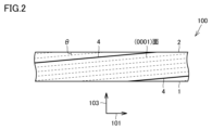
- FIG. 2 is a schematic cross-sectional view taken along line II-II in FIG. 1.
- the cross section shown in FIG. 2 is perpendicular to the first main surface 1 and parallel to the first direction 101.
- silicon carbide substrate 100 according to this embodiment has first main surface 1.
- the first main surface 1 is on the opposite side of the second main surface 2.
- the thickness of silicon carbide substrate 100 is, for example, 300 ⁇ m or more and 700 ⁇ m or less.
- the third direction 103 is a direction perpendicular to each of the first direction 101 and the second direction 102.
- the thickness direction of silicon carbide substrate 100 is the same as third direction 103.
- the off angle ⁇ of the plane inclined in the off direction with respect to the ⁇ 0001 ⁇ plane may be 8° or less.
- the upper limit of the off-angle ⁇ is not particularly limited, but may be, for example, 6° or less, or 4° or less.
- the lower limit of the off-angle ⁇ is not particularly limited, but may be, for example, 1° or more, or 2° or more.
- the off-direction of the plane inclined in the off-direction with respect to the ⁇ 0001 ⁇ plane is, for example, the ⁇ 11-20> direction, although it is not particularly limited.
- silicon carbide substrate 100 has a plurality of basal plane dislocations 4.
- Each of the plurality of basal plane dislocations 4 extends along the (0001) plane.
- basal plane dislocations exposed on first principal surface 1 or second principal surface 2 can be represented as the areal density of basal plane dislocations of silicon carbide substrate 100.
- the areal density of basal plane dislocations 4 is determined using, for example, molten potassium hydroxide (KOH). Specifically, the surface to be measured (for example, the (0001) surface) is etched with molten KOH. As a result, the silicon carbide region near the basal plane dislocations exposed on the surface to be measured is etched, and etch pits are formed on the surface to be measured.
- the temperature of the KOH melt is, for example, 500°C or more and 550°C or less. Etching time is 5 minutes or more and 10 minutes or less.
- etch pits on the surface to be measured are observed using a Normarski differential interference microscope.
- the value obtained by dividing the number of etch pits formed on the surface to be measured by the measurement area on the surface to be measured corresponds to the areal density of basal plane dislocations.
- the observation field of view is, for example, 0.082 cm x 0.070 cm.
- the measurement interval is, for example, 5 mm.
- the areal density of basal plane dislocations 4 on second main surface 2 is 700 cm -2 or more.
- the lower limit of the areal density of basal plane dislocations 4 on the second main surface 2 is not particularly limited, but may be, for example, 800 cm -2 or more, 1000 cm -2 or more, or 1100 cm -2 or more. There may be.
- the upper limit of the areal density of basal plane dislocations 4 on the second principal surface 2 is not particularly limited, but may be, for example, 2000 cm -2 or less, 1500 cm -2 or less, or 1300 cm -2 or less. There may be.
- the areal density of basal plane dislocations 4 on first main surface 1 may be 700 cm ⁇ 2 or more.
- the lower limit of the areal density of basal plane dislocations 4 on the first principal surface 1 is not particularly limited, but may be, for example, 800 cm -2 or more, 1000 cm -2 or more, or 1100 cm -2 or more. There may be.
- the upper limit of the areal density of basal plane dislocations 4 on the first principal surface 1 is not particularly limited, but may be, for example, 2000 cm -2 or less, 1500 cm -2 or less, or 1300 cm -2 or less. There may be.
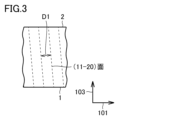
- FIG. 3 is a schematic cross-sectional view taken along line III-III in FIG. 1.
- the area shown in FIG. 3 corresponds to the outer circumference 20.
- the lattice spacing of the (11-20) plane in the outer peripheral portion 20 is a first lattice spacing D1.
- the first lattice spacing D1 corresponds to the lattice constant in the ⁇ 11-20> direction in the outer peripheral portion 20.
- FIG. 4 is a schematic cross-sectional view taken along line IV-IV in FIG. 1.
- the area shown in FIG. 4 corresponds to the central portion 30.
- the lattice spacing of the (11-20) plane in the central portion 30 is the second lattice spacing D2.
- the second lattice spacing D2 corresponds to the lattice constant in the ⁇ 11-20> direction in the central portion 30.
- the lattice spacing in each of the central portion 30 and the outer peripheral portion 20 can be measured using an X-ray diffraction device (product name: SmartLab) manufactured by Rigaku Corporation.
- the X-ray source is, for example, Cu-K ⁇ 1 ray.
- the tube voltage is, for example, 45 kV.
- the tube current is, for example, 40 mA.
- a 2 ⁇ / ⁇ scanning method on a diffraction surface is used.
- the diffraction plane is the (11-20) plane.
- the value obtained by subtracting the lattice spacing of the (11-20) plane in the central portion 30 from the lattice spacing of the (11-20) plane in the outer peripheral portion 20 is as follows: -0.00081 nm or more and 0.00065 nm or less.
- the value obtained by subtracting the lattice spacing of the (11-20) plane in the central portion 30 from the lattice spacing of the (11-20) plane in the outer peripheral portion 20 may be ⁇ 0.00081 nm or more and less than 0 nm.
- the value obtained by subtracting the lattice spacing of the (11-20) plane in the central portion 30 from the lattice spacing of the (11-20) plane in the outer peripheral portion 20 is not particularly limited, but is, for example, -0.00054 nm or more -0. 00017 nm or less, -0.00081 nm or more and -0.00017 nm or less, -0.00054 nm or more and 0.00065 nm or less, or -0.00049 nm or more -0. It may be less than 00022 nm.
- Silicon carbide substrate 100 according to the second embodiment differs from silicon carbide substrate 100 according to the first embodiment in the combination of the areal density of basal plane dislocations 4 and the difference in the lattice spacing of the (11-20) plane.
- the other configurations are substantially the same as silicon carbide substrate 100 according to the first embodiment.
- the structure different from silicon carbide substrate 100 according to the first embodiment will be mainly explained.
- the areal density of basal plane dislocations 4 on second main surface 2 is less than 700 cm ⁇ 2 .
- the lower limit of the areal density of basal plane dislocations 4 on the second main surface 2 is not particularly limited, but may be, for example, 100 cm -2 or more, 200 cm -2 or more, or 250 cm -2 or more. There may be.
- the upper limit of the areal density of basal plane dislocations 4 on the second main surface 2 is not particularly limited, but may be, for example, 500 cm -2 or less, 400 cm -2 or less, or 300 cm -2 or less. There may be.
- the areal density of basal plane dislocations 4 on first main surface 1 is less than 700 cm ⁇ 2 .
- the lower limit of the areal density of basal plane dislocations 4 on the first principal surface 1 is not particularly limited, but may be, for example, 100 cm -2 or more, 200 cm -2 or more, or 250 cm -2 or more. There may be.
- the upper limit of the areal density of basal plane dislocations 4 on the first principal surface 1 is not particularly limited, but may be, for example, 500 cm -2 or less, 400 cm -2 or less, or 300 cm -2 or less. There may be.
- the value obtained by subtracting the lattice spacing of the (11-20) plane in the central portion 30 from the lattice spacing of the (11-20) plane in the outer peripheral portion 20 is as follows: -0.00083 nm or more and -0.00009 nm or less. Even if the value obtained by subtracting the lattice spacing of the (11-20) plane in the central part 30 from the lattice spacing of the (11-20) plane in the outer peripheral part 20 is -0.00083 nm or more and -0.00019 nm or less good.
- the value obtained by subtracting the lattice spacing of the (11-20) plane in the central portion 30 from the lattice spacing of the (11-20) plane in the outer peripheral portion 20 is not particularly limited, but is, for example, -0.00083 nm or more -0. 00024 nm or less, -0.00056 nm or more and -0.00009 nm or less, -0.00056 nm or more and -0.00024 nm or less, or -0.00051 nm or more -0 It may be .00029 nm or less.
- FIG. 5 is a schematic partial cross-sectional view showing the configuration of an apparatus for manufacturing silicon carbide crystal 110 according to the present embodiment.
- an apparatus 300 for manufacturing silicon carbide crystal 110 mainly includes a first crucible 130, a first heat insulating material 145, and an induction heating coil 140.
- the first crucible 130 is made of graphite.
- the first crucible 130 has a first housing section 132 and a first lid section 131.
- the first lid part 131 is arranged on the first accommodating part 132.
- the first heat insulating material 145 is arranged to cover the entire first crucible 130.
- the induction heating coil 140 is arranged in a spiral around the outer periphery of the first heat insulating material 145 . By applying electric power to the induction heating coil 140, the first crucible 130 is heated by electromagnetic induction.
- silicon carbide raw material 153 is placed in first storage portion 132.
- Silicon carbide raw material 153 is, for example, polycrystalline silicon carbide powder.
- the seed substrate 150 is fixed to the first lid part 131 using, for example, an adhesive (not shown).
- Seed substrate 150 has a growth surface 151 and a mounting surface 152. Attachment surface 152 is on the opposite side from growth surface 151. Growth surface 151 faces silicon carbide raw material 153.
- the mounting surface 152 faces the first lid portion 131 . Growth surface 151 of seed substrate 150 is arranged to face the surface of silicon carbide raw material 153.
- Seed substrate 150 is, for example, a silicon carbide single crystal substrate whose polytype is 4H.
- the diameter of the growth surface 151 is, for example, 150 mm.
- the diameter of the growth surface 151 may be 150 mm or more.
- the growth surface 151 is, for example, a surface inclined by an off-angle of about 8° or less with respect to the ⁇ 0001 ⁇ plane. As described above, seed substrate 150 and silicon carbide raw material 153 are placed in first crucible 130.
- FIG. 6 is a schematic cross-sectional view showing the growth process of silicon carbide crystal 110.
- the pressure in first crucible 130 is reduced while the temperature of growth surface 151 of seed substrate 150 is lower than the temperature of silicon carbide raw material 153.
- the pressure of the atmospheric gas in the first crucible 130 is reduced to, for example, 1.0 kPa.
- silicon carbide raw material 153 starts to sublimate, and the sublimated silicon carbide gas recrystallizes on growth surface 151 of seed substrate 150 .
- silicon carbide crystal 110 grows as a single crystal. While silicon carbide crystal 110 is growing, the pressure within first crucible 130 is maintained at, for example, approximately 0.1 kPa or more and 3 kPa or less.
- silicon carbide crystal 110 is grown on seed substrate 150 by subliming silicon carbide raw material 153.
- the temperature of silicon carbide crystal 110 is, for example, 2100° C. or higher and 2300° C. or lower.
- the lower limit of the temperature of silicon carbide crystal 110 is not particularly limited, but may be, for example, 2125° C. or higher, or 2150° C. or higher.
- the upper limit of the temperature of silicon carbide crystal 110 is not particularly limited, but may be, for example, 2250° C. or lower or 2275° C. or lower.
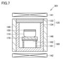
- FIG. 7 is a schematic cross-sectional view showing a step of annealing silicon carbide crystal 110.
- an annealing device 301 for silicon carbide crystal 110 includes a second crucible 135, an upper resistance heater 141, a lower resistance heater 142, a second heat insulating material 146, a support base 160, and a third It mainly has a heat insulating material 170.
- the second crucible 135 is made of graphite.
- the second crucible 135 has a second housing section 134 and a second lid section 133.
- the second lid part 133 is arranged on the second accommodating part 134.
- the second heat insulating material 146 is arranged around the outer peripheral surface of the second crucible 135.
- the second heat insulating material 146 is not arranged at a position facing each of the upper surface and the lower surface of the second crucible 135.
- Upper resistance heater 141 faces the upper surface of second crucible 135 .
- Lower resistance heater 142 faces the lower surface of second crucible 135 .
- the support stand 160 is arranged inside the second accommodating part 134 .
- the support stand 160 has a plate portion 162 and a support portion 161.
- the plate portion 162 is arranged on the support portion 161.
- the third heat insulating material 170 is arranged on the plate portion 162.
- the bulk density of graphite constituting the third heat insulating material 170 is, for example, 0.1 g/cm 3 or more and 0.16 g/cm 3 or less.
- the bulk density of the graphite constituting the support base 160 is, for example, 1.6 g/cm 3 or more and 1.9 g/cm 3 or less.
- Silicon carbide crystal 110 is placed on third heat insulating material 170 . Silicon carbide crystal 110 is in contact with third heat insulating material 170 .
- silicon carbide crystal 110 is heated. No resistance heater is arranged around the outer peripheral surface of silicon carbide crystal 110.
- the thickness of the second heat insulating material 146 is reduced, heat easily escapes from the inside of the second crucible 135 to the outside. Thereby, the difference in temperature between the outer peripheral portion of silicon carbide crystal 110 and the temperature at the central portion of silicon carbide crystal 110 can be reduced.
- the temperature at the outer periphery of silicon carbide crystal 110 may be lower than the temperature at the center of silicon carbide crystal 110.
- silicon carbide crystal 110 is removed from first crucible 130 , it is placed on third heat insulating material 170 in second crucible 135 . Silicon carbide crystal 110 is annealed with silicon carbide crystal 110 disposed on third heat insulating material 170 .
- the difference in coefficient of thermal expansion between silicon carbide crystal 110 and third heat insulating material 170 is smaller than the difference in coefficient of thermal expansion between silicon carbide crystal 110 and first crucible 130 . Therefore, compared to the case where silicon carbide crystal 110 is annealed with silicon carbide crystal 110 attached to first crucible 130, silicon carbide crystal 110 is annealed with silicon carbide crystal 110 disposed on third heat insulating material 170.
- stress in silicon carbide crystal 110 can be effectively alleviated. Thereby, stress in the outer peripheral portion of silicon carbide crystal 110 can be reduced.
- silicon carbide crystal 110 is sliced. Specifically, silicon carbide crystal 110 is sliced along a plane perpendicular to the central axis of silicon carbide crystal 110 using, for example, a saw wire. Thereby, a plurality of silicon carbide substrates 100 according to this embodiment are obtained (see FIG. 2). According to silicon carbide substrate 100 according to the present embodiment, the value obtained by subtracting second lattice spacing D2 from first lattice spacing D1 is a small or negative value.
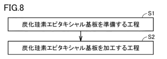
- FIG. 8 is a flowchart schematically showing a method for manufacturing silicon carbide semiconductor device 400 according to this embodiment.
- the method for manufacturing silicon carbide semiconductor device 400 according to the present embodiment includes a step of preparing silicon carbide epitaxial substrate 200 (S1), and a step of processing silicon carbide epitaxial substrate 200 (S2). It mainly has
- a step (S1) of preparing silicon carbide epitaxial substrate 200 is performed.
- silicon carbide substrate 100 according to the first embodiment is prepared (see FIG. 1).
- silicon carbide epitaxial layer 60 is formed on silicon carbide substrate 100.
- silicon carbide epitaxial layer 60 is formed on first main surface 1 of silicon carbide substrate 100 by epitaxial growth.
- silane (SiH 4 ) and propane (C 3 H 8 ) are used as source gases, and hydrogen (H 2 ) is used as a carrier gas.
- the temperature for epitaxial growth is, for example, about 1400° C. or more and 1700° C. or less.
- an n-type impurity, such as nitrogen, is introduced into silicon carbide epitaxial layer 60.
- FIG. 9 is a schematic cross-sectional view showing the configuration of silicon carbide epitaxial substrate 200 according to this embodiment.
- the basal plane dislocation 4 is omitted in the drawings from FIG. 9 onwards.
- silicon carbide epitaxial substrate 200 includes silicon carbide substrate 100 and silicon carbide epitaxial layer 60. Silicon carbide epitaxial layer 60 is provided on silicon carbide substrate 100. Silicon carbide epitaxial layer 60 has third main surface 3 . Third main surface 3 constitutes the surface of silicon carbide epitaxial substrate 200 . Second main surface 2 constitutes the back surface of silicon carbide epitaxial substrate 200 .
- Silicon carbide epitaxial layer 60 may include buffer layer 41 and drift layer 42 .
- Buffer layer 41 is in contact with silicon carbide substrate 100 at first main surface 1 .
- Drift layer 42 is provided on buffer layer 41.
- Each of the buffer layer 41 and the drift layer 42 contains an n-type impurity such as nitrogen.
- the concentration of n-type impurities contained in the buffer layer 41 may be higher than the concentration of n-type impurities contained in the drift layer 42.
- a step (S2) of processing silicon carbide epitaxial substrate 200 is performed. Specifically, the following processing is performed on silicon carbide epitaxial substrate 200. First, ion implantation is performed into silicon carbide epitaxial substrate 200.
- FIG. 10 is a schematic cross-sectional view showing the process of forming the body region.
- a p-type impurity such as aluminum is ion-implanted into third main surface 3 of silicon carbide epitaxial layer 60 .
- body region 113 having p-type conductivity is formed.
- the portion where body region 113 is not formed becomes drift layer 42 and buffer layer 41.
- the thickness of the body region 113 is, for example, 0.9 ⁇ m.
- Silicon carbide epitaxial layer 60 includes buffer layer 41 , drift layer 42 , and body region 113 .
- FIG. 11 is a schematic cross-sectional view showing the process of forming a source region.
- an n-type impurity such as phosphorus is ion-implanted into body region 113, for example.
- a source region 114 having an n-type conductivity type is formed.
- the thickness of the source region 114 is, for example, 0.4 ⁇ m.
- the concentration of n-type impurities contained in source region 114 is higher than the concentration of p-type impurities contained in body region 113.
- a contact region 118 is formed by ion-implanting a p-type impurity such as aluminum into the source region 114.
- Contact region 118 is formed to penetrate source region 114 and body region 113 and be in contact with drift layer 42 .
- the concentration of p-type impurities contained in contact region 118 is higher than the concentration of n-type impurities contained in source region 114.
- activation annealing is performed to activate the ion-implanted impurities.
- the activation annealing temperature is, for example, 1500° C. or more and 1900° C. or less.
- the activation annealing time is, for example, about 30 minutes.
- the activation annealing atmosphere is, for example, an argon atmosphere.
- FIG. 12 is a schematic cross-sectional view showing a step of forming a trench in third main surface 3 of silicon carbide epitaxial layer 60.
- a mask 117 having an opening is formed on the third main surface 3 composed of the source region 114 and the contact region 118. Using mask 117, source region 114, body region 113, and a portion of drift layer 42 are removed by etching.
- the etching method for example, inductively coupled plasma reactive ion etching can be used. Specifically, for example, inductively coupled plasma reactive ion etching using SF 6 or a mixed gas of SF 6 and O 2 as a reactive gas is used. A recess is formed in the third main surface 3 by etching.
- thermal etching is performed in the recesses.
- Thermal etching can be performed, for example, by heating in an atmosphere containing a reactive gas containing at least one type of halogen atom, with the mask 117 formed on the third main surface 3.
- At least one type of halogen atom includes at least one of a chlorine (Cl) atom and a fluorine (F) atom.
- the atmosphere includes, for example, Cl2 , BCl3 , SF6 or CF4 .
- thermal etching is performed using a mixed gas of chlorine gas and oxygen gas as a reaction gas, and at a heat treatment temperature of, for example, 700° C. or higher and 1000° C. or lower.
- the reaction gas may contain a carrier gas in addition to the above-mentioned chlorine gas and oxygen gas.
- the carrier gas for example, nitrogen gas, argon gas, or helium gas can be used.
- trenches 56 are formed in the third main surface 3 by thermal etching.
- Trench 56 is defined by side wall surface 53 and bottom wall surface 54 .
- Sidewall surface 53 is composed of source region 114, body region 113, and drift layer 42.
- the bottom wall surface 54 is composed of the drift layer 42.
- the mask 117 is removed from the third main surface 3.
- FIG. 13 is a schematic cross-sectional view showing the process of forming a gate insulating film.
- silicon carbide epitaxial substrate 200 in which trenches 56 are formed in third main surface 3 is heated at a temperature of, for example, 1300° C. or more and 1400° C. or less in an atmosphere containing oxygen.
- the bottom wall surface 54 is in contact with the drift layer 42
- the side wall surface 53 is in contact with each of the drift layer 42 , the body region 113 , and the source region 114
- the third main surface 3 is in contact with each of the source region 114 and the contact region 118 .
- a contacting gate insulating film 115 is formed.
- FIG. 14 is a schematic cross-sectional view showing the process of forming a gate electrode and an interlayer insulating film.
- Gate electrode 127 is formed inside trench 56 so as to be in contact with gate insulating film 115 .
- Gate electrode 127 is disposed inside trench 56 and formed on gate insulating film 115 so as to face each of side wall surface 53 and bottom wall surface 54 of trench 56 .
- the gate electrode 127 is formed, for example, by LPCVD (Low Pressure Chemical Vapor Deposition) method.
- Interlayer insulating film 126 is formed. Interlayer insulating film 126 is formed to cover gate electrode 127 and to be in contact with gate insulating film 115 .
- the interlayer insulating film 126 is formed, for example, by chemical vapor deposition.
- the interlayer insulating film 126 is made of, for example, a material containing silicon dioxide.
- interlayer insulating film 126 and a portion of gate insulating film 115 are etched so that openings are formed over source region 114 and contact region 118. As a result, contact region 118 and source region 114 are exposed from gate insulating film 115.
- Source electrode 116 is formed so as to be in contact with each of source region 114 and contact region 118.
- Source electrode 116 is formed by, for example, a sputtering method.
- the source electrode 116 is made of a material containing, for example, Ti (titanium), Al (aluminum), and Si (silicon).
- alloying annealing is performed. Specifically, the source electrode 116 in contact with each of the source region 114 and the contact region 118 is maintained at a temperature of, for example, 900° C. or more and 1100° C. or less for about 5 minutes. As a result, at least a portion of the source electrode 116 is silicided. As a result, a source electrode 116 that is in ohmic contact with the source region 114 is formed. Source electrode 116 may be in ohmic contact with contact region 118.
- Source wiring 119 is formed.
- Source wiring 119 is electrically connected to source electrode 116.
- Source wiring 119 is formed to cover source electrode 116 and interlayer insulating film 126 .
- a step of forming a drain electrode is performed. First, silicon carbide substrate 100 is polished on second main surface 2 . This reduces the thickness of silicon carbide substrate 100. Next, drain electrode 123 is formed. Drain electrode 123 is formed so as to be in contact with second main surface 2 . Through the above steps, silicon carbide semiconductor device 400 according to this embodiment is manufactured.
- FIG. 15 is a schematic cross-sectional view showing the configuration of silicon carbide semiconductor device 400 according to this embodiment.
- Silicon carbide semiconductor device 400 is, for example, a MOSFET (Metal Oxide Semiconductor Field Effect Transistor).
- Silicon carbide semiconductor device 400 mainly includes silicon carbide epitaxial substrate 200, gate electrode 127, gate insulating film 115, source electrode 116, drain electrode 123, source wiring 119, and interlayer insulating film 126. ing.
- Silicon carbide epitaxial substrate 200 has buffer layer 41 , drift layer 42 , body region 113 , source region 114 , and contact region 118 .
- Silicon carbide semiconductor device 400 may be, for example, an IGBT (Insulated Gate Bipolar Transistor).
- the outer periphery of the crucible is heated using a heater placed on the outer periphery side of the crucible. Therefore, during crystal growth of silicon carbide crystal 110, the temperature of the outer peripheral portion of silicon carbide crystal 110 is higher than the temperature of the central portion of silicon carbide crystal 110. As a result, compressive stress is generated at the outer periphery of silicon carbide crystal 110.
- silicon carbide substrate 100 includes basal plane dislocations 4
- stress in silicon carbide substrate 100 can be alleviated by movement of basal plane dislocations 4 during the heating process when manufacturing silicon carbide semiconductor device 400. I can do it. Therefore, when the stress of silicon carbide substrate 100 is high, it is desirable that the areal density of basal plane dislocations 4 is high to some extent. On the other hand, if the areal density of basal plane dislocations 4 is excessively high, the reliability of silicon carbide semiconductor device 400 decreases. Therefore, when the stress of silicon carbide substrate 100 is low, it is desirable that the areal density of basal plane dislocations 4 is low to some extent.
- main surface 2 includes central portion 30 and outer peripheral portion 20 located 10 mm away from outer peripheral edge 9 of main surface 2 toward central portion 30. There is.
- the value obtained by subtracting the lattice spacing of the (11-20) plane in the central portion 30 from the lattice spacing of the (11-20) plane in the outer peripheral portion 20 is ⁇ 0.00081 nm or more and 0.00065 nm or less.
- the surface density of basal plane dislocations 4 on the main surface 2 is 700 cm ⁇ 2 or more.
- the basal plane dislocation 4 Since the areal density of silicon carbide substrate 100 is high, stress in silicon carbide substrate 100 can be reduced. Therefore, generation of cracks in silicon carbide substrate 100 can be suppressed.
- the areal density of basal plane dislocations 4 on main surface 2 may be 1000 cm -2 or more. Thereby, generation of cracks in silicon carbide substrate 100 can be further suppressed.
- the value obtained by subtracting the lattice spacing of the (11-20) plane in the central portion 30 from the lattice spacing of the (11-20) plane in the outer peripheral portion 20 is - It may be 0.00054 nm or more and 0.00017 nm or less. Thereby, generation of cracks in silicon carbide substrate 100 can be further suppressed.
- main surface 2 includes central portion 30 and outer peripheral portion 20 located 10 mm away from outer peripheral edge 9 of main surface 2 toward central portion 30. There is.
- the value obtained by subtracting the lattice spacing of the (11-20) plane in the central portion 30 from the lattice spacing of the (11-20) plane in the outer peripheral portion 20 is ⁇ 0.00083 nm or more and ⁇ 0.00009 nm or less.
- the surface density of basal plane dislocations 4 on the main surface 2 is less than 700 cm ⁇ 2 .
- the stress in the silicon carbide substrate 100 can be reduced. can be reduced. Therefore, while suppressing the occurrence of cracks in silicon carbide substrate 100, it is possible to suppress a decrease in reliability of silicon carbide semiconductor device 400.
- the areal density of basal plane dislocations 4 on main surface 2 may be 300 cm ⁇ 2 or less. Thereby, while suppressing the occurrence of cracks in silicon carbide substrate 100, it is possible to further suppress a decrease in reliability of silicon carbide semiconductor device 400.
- the value obtained by subtracting the lattice spacing of the (11-20) plane in the central portion 30 from the lattice spacing of the (11-20) plane in the outer peripheral portion 20 is - It may be 0.00056 nm or more and 0.00024 nm or less.
- main surface 2 When the diameter of main surface 2 is large, the temperature difference between central portion 30 and outer peripheral portion 20 becomes large, making silicon carbide substrate 100 more likely to crack.
- main surface 2 may have a diameter of 150 mm or more. When the diameter of main surface 2 is large, it is possible to effectively suppress the occurrence of cracks in silicon carbide substrate 100.
- the diameter of main surface 2 may be 200 mm or more.
- the diameter of main surface 2 is large, it is possible to effectively suppress the occurrence of cracks in silicon carbide substrate 100.
- silicon carbide crystal 110 was manufactured using manufacturing conditions related to Samples 1 to 8. Under the manufacturing conditions for Samples 1 to 8, a step of growing silicon carbide crystal 110 by a sublimation method was performed. Specifically, silicon carbide crystal 110 was manufactured using the first crucible shown in FIG.
- the annealing process for silicon carbide crystal 110 was not performed after the silicon carbide crystal 110 growth process. Under the manufacturing conditions for Samples 3 to 8, the annealing process for silicon carbide crystal 110 was performed after the silicon carbide crystal 110 growth process. Specifically, an annealing process for silicon carbide crystal 110 was performed using annealing apparatus 301 shown in FIG.
- the temperature of central portion 30 of silicon carbide crystal 110 was 2200°C.
- the pressure inside the annealing device 301 was 90 kPa.
- the atmosphere gas was argon gas.
- the annealing time was 5 hours.
- silicon carbide crystal 110 was sliced using a saw wire. As a result, three silicon carbide substrates 100 were cut out. Each of three silicon carbide substrates 100 has a first main surface 1 and a second main surface 2.
- the second principal surface 2 was a surface inclined in the off direction with respect to the ⁇ 0001 ⁇ plane.
- the off direction was set to ⁇ 11-20>.
- the off angle ⁇ was 4°.
- silicon carbide substrates 100 manufactured using the manufacturing conditions of each of Samples 1 to 8 were prepared.
- the lattice spacing in each of the central portion 30 and outer peripheral portion 20 of the second principal surface 2 was measured using an X-ray diffraction device (product name: SmartLab) manufactured by Rigaku Co., Ltd.
- the X-ray source was Cu-K ⁇ 1 ray.
- the tube voltage was 45 kV.
- the tube current was 40 mA.
- a 2 ⁇ / ⁇ scanning method on a diffraction surface was used.
- the diffraction plane was the (11-20) plane.
- the value obtained by subtracting the lattice spacing of the (11-20) plane in the central part 30 from the lattice spacing of the (11-20) plane in the outer peripheral part 20 is taken as the difference in the lattice spacing of the (11-20) plane. .
- the areal density of basal plane dislocations 4 was determined using molten potassium hydroxide (KOH).
- KOH molten potassium hydroxide
- the temperature of the KOH melt was 500°C or more and 550°C or less.
- the etching time was 5 minutes or more and 10 minutes or less.
- etch pits on the surface to be measured were observed using a Normarski differential interference microscope.
- the observation field was 0.082 cm x 0.070 cm.
- the measurement interval was 5 mm.
- Table 1 shows the difference in the lattice spacing of the (11-20) plane in the silicon carbide substrates 100 of each of Samples 1 to 8, the areal density of basal plane dislocations 4 in the second principal surface 2, and the presence or absence of cracks. It shows.
- a silicon carbide substrate having a main surface having a main surface, The main surface includes a central part and an outer peripheral part located 10 mm away from the outer peripheral edge of the main surface toward the central part, The value obtained by subtracting the lattice spacing of the (11-20) plane in the central portion from the lattice spacing of the (11-20) plane in the outer peripheral portion is ⁇ 0.00081 nm or more and 0.00065 nm or less,
- the silicon carbide substrate has a surface density of basal plane dislocations on the main surface of 700 cm -2 or more.
- the silicon carbide substrate according to Supplementary Note 1 wherein the surface density of basal plane dislocations on the main surface is 1000 cm -2 or more.
- (Appendix 9) The silicon carbide substrate according to any one of Supplementary notes 1 to 8, wherein the main surface has a diameter of 150 mm or more.
- (Appendix 10) The silicon carbide substrate according to appendix 9, wherein the main surface has a diameter of 200 mm or more.
- (Appendix 11) The silicon carbide substrate according to any one of Supplementary notes 1 to 8, A silicon carbide epitaxial substrate, comprising: a silicon carbide epitaxial layer provided on the silicon carbide substrate.
- (Appendix 12) A step of preparing a silicon carbide epitaxial substrate according to Appendix 11; A method for manufacturing a silicon carbide semiconductor device, comprising the step of processing the silicon carbide epitaxial substrate.
Landscapes
- Chemical & Material Sciences (AREA)
- Engineering & Computer Science (AREA)
- Crystallography & Structural Chemistry (AREA)
- Materials Engineering (AREA)
- Metallurgy (AREA)
- Organic Chemistry (AREA)
- Chemical Kinetics & Catalysis (AREA)
- General Chemical & Material Sciences (AREA)
- Inorganic Chemistry (AREA)
- Crystals, And After-Treatments Of Crystals (AREA)
Abstract
炭化珪素基板は、主面を有している。主面は、中央部と、主面の外周縁から中央部に向かって10mm離れた位置にある外周部とを含んでいる。外周部における(11-20)面の格子面間隔から、中央部における(11-20)面の格子面間隔を差し引いた値は、-0.00081nm以上0.00065nm以下である。主面における基底面転位の面密度は、700cm-2以上である。
Description
本開示は、炭化珪素基板、炭化珪素エピタキシャル基板および炭化珪素半導体装置の製造方法に関する。本出願は、2022年7月14日に出願した日本特許出願である特願2022-113414号に基づく優先権を主張する。当該日本特許出願に記載された全ての記載内容は、参照によって本明細書に援用される。
特開2014-185055号公報(特許文献1)には、<0001>方向の格子定数の最大値と最小値との差が0.004nm以下であるインゴットが記載されている。
本開示に係る炭化珪素基板は、主面を有している。主面は、中央部と、主面の外周縁から中央部に向かって10mm離れた位置にある外周部とを含んでいる。外周部における(11-20)面の格子面間隔から、中央部における(11-20)面の格子面間隔を差し引いた値は、-0.00081nm以上0.00065nm以下である。主面における基底面転位の面密度は、700cm-2以上である。
[本開示が解決しようとする課題]
本開示の目的は、クラックの発生を抑制可能な炭化珪素基板、炭化珪素エピタキシャル基板および炭化珪素半導体装置の製造方法を提供することである。
[本開示の効果]
[本開示の効果]
本開示によれば、クラックの発生を抑制可能な炭化珪素基板、炭化珪素エピタキシャル基板および炭化珪素半導体装置の製造方法を提供することができる。
[本開示の実施形態の説明]
最初に本開示の実施形態を列記して説明する。
(1)本開示に係る炭化珪素基板100は、主面2を有している。主面2は、中央部30と、主面2の外周縁9から中央部30に向かって10mm離れた位置にある外周部20とを含んでいる。外周部20における(11-20)面の格子面間隔から、中央部30における(11-20)面の格子面間隔を差し引いた値は、-0.00081nm以上0.00065nm以下である。主面2における基底面転位4の面密度は、700cm-2以上である。これにより、外周部20における(11-20)面の格子面間隔から、中央部30における(11-20)面の格子面間隔を差し引いた値がある程度大きい場合であっても、基底面転位4の面密度が高いため、炭化珪素基板100の応力を低減することができる。そのため、炭化珪素基板100にクラックが発生することを抑制することができる。
(2)上記(1)に係る炭化珪素基板100によれば、主面2における基底面転位4の面密度は、1000cm-2以上であってもよい。これにより、炭化珪素基板100にクラックが発生することをさらに抑制することができる。
(3)上記(1)または(2)に係る炭化珪素基板100によれば、外周部20における(11-20)面の格子面間隔から、中央部30における(11-20)面の格子面間隔を差し引いた値は、-0.00054nm以上-0.00017nm以下であってもよい。これにより、炭化珪素基板100にクラックが発生することをさらに抑制することができる。
(4)本開示に係る炭化珪素基板100は、主面2を有している。主面2は、中央部30と、主面2の外周縁9から中央部30に向かって10mm離れた位置にある外周部20とを含んでいる。外周部20における(11-20)面の格子面間隔から、中央部30における(11-20)面の格子面間隔を差し引いた値は、-0.00083nm以上-0.00009nm以下である。主面2における基底面転位4の面密度は、700cm-2未満である。これにより、外周部20における(11-20)面の格子面間隔から、中央部30における(11-20)面の格子面間隔を差し引いた値がある程度小さい場合において、炭化珪素基板100の応力を低減することができる。そのため、炭化珪素基板100にクラックが発生することを抑制しつつ、炭化珪素半導体装置400の信頼性が低下することを抑制することができる。
(5)上記(4)に係る炭化珪素基板100によれば、主面2における基底面転位4の面密度は、300cm-2以下であってもよい。これにより、炭化珪素基板100にクラックが発生することを抑制しつつ、炭化珪素半導体装置400の信頼性が低下することをさらに抑制することができる。
(6)上記(4)または(5)に係る炭化珪素基板100によれば、外周部20における(11-20)面の格子面間隔から、中央部30における(11-20)面の格子面間隔を差し引いた値は、-0.00056nm以上-0.00024nm以下であってもよい。これにより、炭化珪素基板100にクラックが発生することをさらに抑制しつつ、炭化珪素半導体装置400の信頼性が低下することをさらに抑制することができる。
(7)上記(1)から(6)のいずれかに係る炭化珪素基板100によれば、主面2の直径は、150mm以上であってもよい。主面2の直径が大きい場合において、炭化珪素基板100にクラックが発生することを効果的に抑制することができる。
(8)上記(7)に係る炭化珪素基板100によれば、主面2の直径は、200mm以上であってもよい。主面2の直径が大きい場合において、炭化珪素基板100にクラックが発生することを効果的に抑制することができる。
(9)本開示に係る炭化珪素エピタキシャル基板200は、上記(1)から(8)のいずれかに係る炭化珪素基板100と、炭化珪素基板100上に設けられた炭化珪素エピタキシャル層60と、を備えている。
(10)本開示に係る炭化珪素半導体装置400の製造方法は、以下の工程を備えている。上記(9)に記載の炭化珪素エピタキシャル基板200が準備される。炭化珪素エピタキシャル基板200が加工される。
[本開示の実施形態の詳細]
以下、図面に基づいて、本開示の実施形態の詳細について説明する。なお、以下の図面において同一または相当する部分には同一の参照番号を付し、その説明は繰返さない。本明細書中の結晶学的記載においては、個別方位を[]、集合方位を<>、個別面を()、集合面を{}でそれぞれ示している。また、負の指数については、結晶学上、”-”(バー)を数字の上に付けることになっているが、本明細書中では、数字の前に負の符号を付けている。
[本開示の実施形態の詳細]
以下、図面に基づいて、本開示の実施形態の詳細について説明する。なお、以下の図面において同一または相当する部分には同一の参照番号を付し、その説明は繰返さない。本明細書中の結晶学的記載においては、個別方位を[]、集合方位を<>、個別面を()、集合面を{}でそれぞれ示している。また、負の指数については、結晶学上、”-”(バー)を数字の上に付けることになっているが、本明細書中では、数字の前に負の符号を付けている。
まず、第1実施形態に係る炭化珪素基板100の構成について説明する。図1は、第1実施形態に係る炭化珪素基板100の構成を示す平面模式図である。
図1に示されるように、第1実施形態に係る炭化珪素基板100は、主面2(第2主面2)を有している。第2主面2は、第1方向101および第2方向102の各々に沿って拡がっている。第1方向101は、特に限定されないが、たとえば<11-20>方向である。第2方向102は、特に限定されないが、たとえば<1-100>方向である。オフ方向は、たとえば第1方向101である。炭化珪素基板100は、たとえば六方晶炭化珪素により構成されている。六方晶炭化珪素のポリタイプは、たとえば4Hである。炭化珪素基板100は、たとえば窒素などのn型不純物を含んでいる。
第2主面2は、{0001}面または{0001}面に対してオフ方向に傾斜した面である。第2主面2は、たとえば(0001)面または(0001)面に対してオフ方向に傾斜した面である。この場合、第1主面1(図2参照)は、たとえば(000-1)面または(000-1)面に対してオフ方向に傾斜した面である。第2主面2は、たとえば(000-1)面または(000-1)面に対してオフ方向に傾斜した面であってもよい。この場合、第1主面1(図2参照)は、たとえば(0001)面または(0001)面に対してオフ方向に傾斜した面である。
図1に示されるように、第2主面2の外周縁9は、オリエンテーションフラット部7と、円弧状部8とを有している。円弧状部8は、オリエンテーションフラット部7に連なっている。図1に示されるように、第2主面2に対して垂直な方向から見て、オリエンテーションフラット部7は、第1方向101に沿って延在している。
第2主面2の直径W1は、たとえば150mmである。直径W1は、150mm以上でもよいし、200mm以上でもよい。直径W1の上限は、特に限定されないが、たとえば300mm以下であってもよい。第2主面2に対して垂直な方向に見て、直径W1は、外周縁9上の異なる2点間の最長直線距離である。
図1に示されるように、第2主面2は、中央部30と、外周部20とを有している。中央部30は、第2主面2の中心に位置している。第2主面2に対して垂直な方向に見て、中央部30は、円弧状部8を含む円の中心に位置している。外周部20は、第2主面2の外周縁9から中央部30に向かって10mm離れた位置にある。別の観点から言えば、第2主面2の中心から外側に向かう径方向において、外周部20と外周縁9との距離W2は10mmである。
外周部20は、第1外周位置21と、第2外周位置22と、第3外周位置23と、第4外周位置24とを有している。第1外周位置21は、中央部30に対して第1方向101に離れた位置にある。第2外周位置22は、中央部30を中心として、第1外周位置21が90°時計回りに回転移動した位置にある。第4外周位置24は、中央部30を中心として、第2外周位置22が90°時計回りに回転移動した位置にある。第3外周位置23は、中央部30を中心として、第4外周位置24が90°時計回りに回転移動した位置にある。
第2主面2に対して垂直でありかつ第2主面2から第1主面1に向かう方向に見た場合、第4外周位置24と、中央部30と、第1外周位置21とは、第1方向101に平行な直線上に位置している。同様に、第2主面2に対して垂直でありかつ第2主面2から第1主面1に向かう方向に見た場合、第2外周位置22と、中央部30と、第3外周位置23とは、第2方向102に平行な直線上に位置している。
図2は、図1のII-II線に沿った断面模式図である。図2に示される断面は、第1主面1に対して垂直であり、かつ第1方向101に平行である。図2に示されるように、本実施形態に係る炭化珪素基板100は、第1主面1を有している。第1主面1は、第2主面2の反対側にある。炭化珪素基板100の厚みは、たとえば300μm以上700μm以下である。第3方向103は、第1方向101および第2方向102の各々に対して垂直な方向である。炭化珪素基板100の厚み方向は、第3方向103と同じである。
第2主面2が{0001}面に対してオフ方向に傾斜している場合、{0001}面に対してオフ方向に傾斜した面のオフ角度θは、8°以下であってもよい。オフ角度θの上限は、特に限定されないが、たとえば6°以下であってもよいし、4°以下であってもよい。オフ角度θの下限は、特に限定されないが、たとえば1°以上であってもよいし、2°以上であってもよい。{0001}面に対してオフ方向に傾斜した面のオフ方向は、特に限定されないが、たとえば<11-20>方向である。
図2に示されるように、炭化珪素基板100は、複数の基底面転位4を有している。複数の基底面転位4の各々は、(0001)面に沿って延在している。たとえば第1主面1または第2主面2に露出している基底面転位を、炭化珪素基板100の基底面転位の面密度として代表させることができる。
次に、基底面転位4の面密度の測定方法について説明する。
基底面転位4の面密度は、たとえば溶融水酸化カリウム(KOH)を用いて決定される。具体的には、被測定面(たとえば、(0001)面)が、溶融KOHによってエッチングされる。これにより、被測定面に露出した基底面転位の付近にある炭化珪素領域がエッチングされ、被測定面にエッチピットが形成される。KOH融液の温度は、たとえば500℃以上550℃以下とする。エッチング時間は、5分以上10分以下とする。
基底面転位4の面密度は、たとえば溶融水酸化カリウム(KOH)を用いて決定される。具体的には、被測定面(たとえば、(0001)面)が、溶融KOHによってエッチングされる。これにより、被測定面に露出した基底面転位の付近にある炭化珪素領域がエッチングされ、被測定面にエッチピットが形成される。KOH融液の温度は、たとえば500℃以上550℃以下とする。エッチング時間は、5分以上10分以下とする。
エッチング後、被測定面におけるエッチピットが、ノルマルスキー微分干渉顕微鏡を用いて観察される。被測定面に形成されたエッチピットの数を、被測定面における測定面積で除した値が、基底面転位の面密度に対応する。観察視野は、たとえば0.082cm×0.070cmとする。測定間隔は、たとえば5mmとする。
第1実施形態に係る炭化珪素基板100によれば、第2主面2における基底面転位4の面密度は、700cm-2以上である。第2主面2における基底面転位4の面密度の下限は、特に限定されないが、たとえば800cm-2以上であってもよいし、1000cm-2以上であってもよいし、1100cm-2以上であってもよい。第2主面2における基底面転位4の面密度の上限は、特に限定されないが、たとえば2000cm-2以下であってもよいし、1500cm-2以下であってもよいし、1300cm-2以下であってもよい。
第1実施形態に係る炭化珪素基板100によれば、第1主面1における基底面転位4の面密度は、700cm-2以上であってもよい。第1主面1における基底面転位4の面密度の下限は、特に限定されないが、たとえば800cm-2以上であってもよいし、1000cm-2以上であってもよいし、1100cm-2以上であってもよい。第1主面1における基底面転位4の面密度の上限は、特に限定されないが、たとえば2000cm-2以下であってもよいし、1500cm-2以下であってもよいし、1300cm-2以下であってもよい。
図3は、図1のIII-III線に沿った断面模式図である。図3に示される領域は、外周部20に対応している。図3に示されるように、外周部20における(11-20)面の格子面間隔は、第1格子面間隔D1とする。第1格子面間隔D1は、外周部20における<11-20>方向の格子定数に対応する。
図4は、図1のIV-IV線に沿った断面模式図である。図4に示される領域は、中央部30に対応している。図3に示されるように、中央部30における(11-20)面の格子面間隔は、第2格子面間隔D2とする。第2格子面間隔D2は、中央部30における<11-20>方向の格子定数に対応する。
次に、格子面間隔の測定方法について説明する。
中央部30および外周部20の各々における格子面間隔は、株式会社リガク製のX線回折装置(製品名:SmartLab)を用いて測定することができる。X線源は、たとえばCu-Kα1線とする。管電圧は、たとえば45kVとする。管電流は、たとえば40mAとする。測定方法として、回折面での2θ/ωスキャン法が使用される。回折面は(11-20)面とする。
中央部30および外周部20の各々における格子面間隔は、株式会社リガク製のX線回折装置(製品名:SmartLab)を用いて測定することができる。X線源は、たとえばCu-Kα1線とする。管電圧は、たとえば45kVとする。管電流は、たとえば40mAとする。測定方法として、回折面での2θ/ωスキャン法が使用される。回折面は(11-20)面とする。
第1実施形態に係る炭化珪素基板100によれば、外周部20における(11-20)面の格子面間隔から、中央部30における(11-20)面の格子面間隔を差し引いた値は、-0.00081nm以上0.00065nm以下である。外周部20における(11-20)面の格子面間隔から、中央部30における(11-20)面の格子面間隔を差し引いた値は、-0.00081nm以上0nm未満であってもよい。
外周部20における(11-20)面の格子面間隔から、中央部30における(11-20)面の格子面間隔を差し引いた値は、特に限定されないが、たとえば-0.00054nm以上-0.00017nm以下であってもよいし、-0.00081nm以上-0.00017nm以下であってもよいし、-0.00054nm以上0.00065nm以下であってもよいし、-0.00049nm以上-0.00022nm以下であってもよい。
次に、第2実施形態に係る炭化珪素基板100の構成について説明する。第2実施形態に係る炭化珪素基板100は、基底面転位4の面密度と、(11-20)面の格子面間隔の差との組み合わせにおいて、第1実施形態に係る炭化珪素基板100と異なっており、その他の構成については、第1実施形態に係る炭化珪素基板100と実質的に同じである。以下、第1実施形態に係る炭化珪素基板100と異なる構成を中心に説明する。
第2実施形態に係る炭化珪素基板100によれば、第2主面2における基底面転位4の面密度は、700cm-2未満である。第2主面2における基底面転位4の面密度の下限は、特に限定されないが、たとえば100cm-2以上であってもよいし、200cm-2以上であってもよいし、250cm-2以上であってもよい。第2主面2における基底面転位4の面密度の上限は、特に限定されないが、たとえば500cm-2以下であってもよいし、400cm-2以下であってもよいし、300cm-2以下であってもよい。
第2実施形態に係る炭化珪素基板100によれば、第1主面1における基底面転位4の面密度は、700cm-2未満である。第1主面1における基底面転位4の面密度の下限は、特に限定されないが、たとえば100cm-2以上であってもよいし、200cm-2以上であってもよいし、250cm-2以上であってもよい。第1主面1における基底面転位4の面密度の上限は、特に限定されないが、たとえば500cm-2以下であってもよいし、400cm-2以下であってもよいし、300cm-2以下であってもよい。
第2実施形態に係る炭化珪素基板100によれば、外周部20における(11-20)面の格子面間隔から、中央部30における(11-20)面の格子面間隔を差し引いた値は、-0.00083nm以上-0.00009nm以下である。外周部20における(11-20)面の格子面間隔から、中央部30における(11-20)面の格子面間隔を差し引いた値は、-0.00083nm以上-0.00019nm以下であってもよい。
外周部20における(11-20)面の格子面間隔から、中央部30における(11-20)面の格子面間隔を差し引いた値は、特に限定されないが、たとえば-0.00083nm以上-0.00024nm以下であってもよいし、-0.00056nm以上-0.00009nm以下であってもよいし、-0.00056nm以上-0.00024nm以下であってもよいし、-0.00051nm以上-0.00029nm以下であってもよい。
<炭化珪素基板の製造方法>
次に、本実施形態に係る炭化珪素基板100の製造方法について説明する。図5は、本実施形態に係る炭化珪素結晶110の製造装置の構成を示す一部断面模式図である。図5に示されるように、炭化珪素結晶110の製造装置300は、第1坩堝130と、第1断熱材145と、誘導加熱コイル140とを主に有している。
次に、本実施形態に係る炭化珪素基板100の製造方法について説明する。図5は、本実施形態に係る炭化珪素結晶110の製造装置の構成を示す一部断面模式図である。図5に示されるように、炭化珪素結晶110の製造装置300は、第1坩堝130と、第1断熱材145と、誘導加熱コイル140とを主に有している。
第1坩堝130は、黒鉛製である。第1坩堝130は、第1収容部132と、第1蓋部131とを有している。第1蓋部131は、第1収容部132上に配置される。第1断熱材145は、第1坩堝130の全体を覆うように配置されている。誘導加熱コイル140は、第1断熱材145の外周の周りにおいて螺旋状に配置されている。誘導加熱コイル140に対して電力が印加されることにより、第1坩堝130が電磁誘導により加熱される。
図5に示されるように、炭化珪素原料153が第1収容部132に配置される。炭化珪素原料153は、たとえば多結晶炭化珪素の粉末である。種基板150は、たとえば接着剤(図示せず)を用いて第1蓋部131に固定される。種基板150は、成長面151と、取付面152とを有している。取付面152は、成長面151と反対側にある。成長面151は、炭化珪素原料153に対向する。取付面152は、第1蓋部131に対向する。種基板150の成長面151は、炭化珪素原料153の表面に対向するように配置される。
種基板150は、たとえばポリタイプが4Hである炭化珪素単結晶基板である。成長面151の直径は、たとえば150mmである。成長面151の直径は、150mm以上であってもよい。成長面151は、たとえば{0001}面に対して8°以下程度のオフ角だけ傾斜した面である。以上のように、種基板150と炭化珪素原料153とは、第1坩堝130に配置される。
図6は、炭化珪素結晶110の成長工程を示す断面模式図である。まず、種基板150の成長面151の温度が炭化珪素原料153の温度よりも低い状態で、第1坩堝130内の圧力が低減される。第1坩堝130内の雰囲気ガスの圧力が、たとえば1.0kPaまで減圧される。これにより、炭化珪素原料153が昇華を開始し、昇華した炭化珪素ガスが種基板150の成長面151において再結晶化する。成長面151上において、炭化珪素結晶110が単結晶成長する。炭化珪素結晶110が成長している間、第1坩堝130内の圧力は、たとえば0.1kPa以上3kPa以下程度に維持される。
以上のように、炭化珪素原料153を昇華することにより種基板150上に炭化珪素結晶110を成長させる。炭化珪素結晶110を成長させる工程において、炭化珪素結晶110の温度は、たとえば2100℃以上2300℃以下である。炭化珪素結晶110の温度の下限は、特に限定されないが、たとえば2125℃以上であってもよいし、2150℃以上であってもよい。炭化珪素結晶110の温度の上限は、特に限定されないが、たとえば2250℃以下であってもよいし、2275℃以下であってもよい。
図7は、炭化珪素結晶110をアニールする工程を示す断面模式図である。図7に示されるように、炭化珪素結晶110のアニール装置301は、第2坩堝135と、上部抵抗ヒータ141と、下部抵抗ヒータ142と、第2断熱材146と、支持台160と、第3断熱材170とを主に有している。第2坩堝135は、黒鉛製である。第2坩堝135は、第2収容部134と、第2蓋部133とを有している。第2蓋部133は、第2収容部134上に配置される。
第2断熱材146は、第2坩堝135の外周面の周りに配置されている。第2断熱材146は、第2坩堝135の上面および下面の各々に対向する位置には配置されていない。上部抵抗ヒータ141は、第2坩堝135の上面に対向している。下部抵抗ヒータ142は、第2坩堝135の下面に対向している。
支持台160は、第2収容部134の内部に配置される。支持台160は、板部162と、支持部161とを有している。板部162は、支持部161上に配置されている。第3断熱材170は、板部162上に配置されている。第3断熱材170を構成する黒鉛のかさ密度は、たとえば0.1g/cm3以上0.16g/cm3以下である。支持台160を構成する黒鉛のかさ密度は、たとえば1.6g/cm3以上1.9g/cm3以下である。炭化珪素結晶110は、第3断熱材170上に配置される。炭化珪素結晶110は、第3断熱材170に接している。
上部抵抗ヒータ141および下部抵抗ヒータ142に電力が印加されることにより、炭化珪素結晶110が加熱される。炭化珪素結晶110の外周面の周りには抵抗ヒータが配置されていない。第2断熱材146の厚みを小さくすると、第2坩堝135の内部から外部に熱が逃げやすくなる。これにより、炭化珪素結晶110の外周部の温度と炭化珪素結晶110の中央部の温度の差を低減することができる。炭化珪素結晶110の外周部の温度は、炭化珪素結晶110の中央部の温度よりも低くてもよい。
炭化珪素結晶110は、第1坩堝130から取り外された後、第2坩堝135において、第3断熱材170上に配置される。炭化珪素結晶110が第3断熱材170上に配置された状態で、炭化珪素結晶110がアニールされる。炭化珪素結晶110と第3断熱材170との熱膨張係数の差は、炭化珪素結晶110と第1坩堝130との熱膨張係数の差よりも小さい。そのため、炭化珪素結晶110が第1坩堝130に取り付けられた状態で炭化珪素結晶110がアニールされる場合と比較して、炭化珪素結晶110が第3断熱材170上に配置された状態で炭化珪素結晶110がアニールされる場合は、炭化珪素結晶110の応力を効果的に緩和することができる。これにより、炭化珪素結晶110の外周部における応力を低減することができる。
次に、炭化珪素結晶110がスライスされる。具体的には、たとえばソーワイヤーを用いて、炭化珪素結晶110の中心軸に垂直な平面に沿って、炭化珪素結晶110がスライスされる。これにより、本実施形態に係る複数の炭化珪素基板100が得られる(図2参照)。本実施形態に係る炭化珪素基板100によれば、第1格子面間隔D1から第2格子面間隔D2を差し引いた値が小さいまたは負の値となる。
<炭化珪素半導体装置の製造方法>
次に、本実施形態に係る炭化珪素半導体装置400の製造方法について説明する。図8は、本実施形態に係る炭化珪素半導体装置400の製造方法を概略的に示すフローチャートである。図8に示されるように、本実施形態に係る炭化珪素半導体装置400の製造方法は、炭化珪素エピタキシャル基板200を準備する工程(S1)と、炭化珪素エピタキシャル基板200を加工する工程(S2)とを主に有している。
次に、本実施形態に係る炭化珪素半導体装置400の製造方法について説明する。図8は、本実施形態に係る炭化珪素半導体装置400の製造方法を概略的に示すフローチャートである。図8に示されるように、本実施形態に係る炭化珪素半導体装置400の製造方法は、炭化珪素エピタキシャル基板200を準備する工程(S1)と、炭化珪素エピタキシャル基板200を加工する工程(S2)とを主に有している。
まず、炭化珪素エピタキシャル基板200を準備する工程(S1)が実施される。炭化珪素エピタキシャル基板200を準備する工程(S1)においては、まず、第1実施形態に係る炭化珪素基板100が準備される(図1参照)。
次に、炭化珪素基板100上に炭化珪素エピタキシャル層60が形成される。具体的には、炭化珪素基板100の第1主面1上に炭化珪素エピタキシャル層60がエピタキシャル成長により形成される。エピタキシャル成長においては、原料ガスとしてたとえばシラン(SiH4)およびプロパン(C3H8)が用いられ、キャリアガスとして水素(H2)が用いられる。エピタキシャル成長の温度は、たとえば1400℃以上1700℃以下程度である。エピタキシャル成長において、たとえば窒素などのn型不純物が、炭化珪素エピタキシャル層60に導入される。以上により、本実施形態に係る炭化珪素エピタキシャル基板200が準備される。
図9は、本実施形態に係る炭化珪素エピタキシャル基板200の構成を示す断面模式図である。説明の便宜のため、図9以降の図面においては、基底面転位4は、省略されている。
図9に示されるように、炭化珪素エピタキシャル基板200は、炭化珪素基板100と、炭化珪素エピタキシャル層60とを有している。炭化珪素エピタキシャル層60は、炭化珪素基板100上に設けられている。炭化珪素エピタキシャル層60は、第3主面3を有している。第3主面3は、炭化珪素エピタキシャル基板200の表面を構成する。第2主面2は、炭化珪素エピタキシャル基板200の裏面を構成する。
炭化珪素エピタキシャル層60は、バッファ層41と、ドリフト層42とを有していてもよい。バッファ層41は、第1主面1において、炭化珪素基板100に接している。ドリフト層42は、バッファ層41上に設けられている。バッファ層41およびドリフト層42の各々は、たとえば窒素などのn型不純物を含んでいる。バッファ層41が含むn型不純物の濃度は、ドリフト層42が含むn型不純物の濃度よりも高くてもよい。
次に、炭化珪素エピタキシャル基板200を加工する工程(S2)が実施される。具体的には、炭化珪素エピタキシャル基板200に対して以下のような加工が行われる。まず、炭化珪素エピタキシャル基板200に対してイオン注入が行われる。
図10は、ボディ領域を形成する工程を示す断面模式図である。ボディ領域を形成する工程において、炭化珪素エピタキシャル層60の第3主面3に対して、たとえばアルミニウムなどのp型不純物がイオン注入される。これにより、p型の導電型を有するボディ領域113が形成される。ボディ領域113が形成されなかった部分は、ドリフト層42およびバッファ層41となる。ボディ領域113の厚みは、たとえば0.9μmである。炭化珪素エピタキシャル層60は、バッファ層41と、ドリフト層42と、ボディ領域113とを含む。
次に、ソース領域を形成する工程が実施される。図11は、ソース領域を形成する工程を示す断面模式図である。具体的には、ボディ領域113に対して、たとえばリンなどのn型不純物がイオン注入される。これにより、n型の導電型を有するソース領域114が形成される。ソース領域114の厚みは、たとえば0.4μmである。ソース領域114が含むn型不純物の濃度は、ボディ領域113が含むp型不純物の濃度よりも高い。
次に、ソース領域114に対して、たとえばアルミニウムなどのp型不純物がイオン注入されることにより、コンタクト領域118が形成される。コンタクト領域118は、ソース領域114およびボディ領域113を貫通し、ドリフト層42に接するように形成される。コンタクト領域118が含むp型不純物の濃度は、ソース領域114が含むn型不純物の濃度よりも高い。
次に、イオン注入された不純物を活性化するため活性化アニールが実施される。活性化アニールの温度は、たとえば1500℃以上1900℃以下である。活性化アニールの時間は、たとえば30分程度である。活性化アニールの雰囲気は、たとえばアルゴン雰囲気である。
次に、炭化珪素エピタキシャル層60の第3主面3にトレンチを形成する工程が実施される。図12は、炭化珪素エピタキシャル層60の第3主面3にトレンチを形成する工程を示す断面模式図である。ソース領域114およびコンタクト領域118から構成される第3主面3上に、開口を有するマスク117が形成される。マスク117を用いて、ソース領域114と、ボディ領域113と、ドリフト層42の一部とがエッチングにより除去される。エッチングの方法としては、たとえば誘導結合プラズマ反応性イオンエッチングを用いることができる。具体的には、たとえば反応ガスとしてSF6またはSF6とO2との混合ガスを用いた誘導結合プラズマ反応性イオンエッチングが用いられる。エッチングにより、第3主面3に凹部が形成される。
次に、凹部において熱エッチングが行われる。熱エッチングは、第3主面3上にマスク117が形成された状態で、たとえば、少なくとも1種類以上のハロゲン原子を有する反応性ガスを含む雰囲気中での加熱によって行い得る。少なくとも1種類以上のハロゲン原子は、塩素(Cl)原子およびフッ素(F)原子の少なくともいずれかを含む。当該雰囲気は、たとえば、Cl2、BCl3、SF6またはCF4を含む。たとえば、塩素ガスと酸素ガスとの混合ガスを反応ガスとして用い、熱処理温度を、たとえば700℃以上1000℃以下として、熱エッチングが行われる。なお、反応ガスは、上述した塩素ガスと酸素ガスとに加えて、キャリアガスを含んでいてもよい。キャリアガスとしては、たとえば窒素ガス、アルゴンガスまたはヘリウムガスなどを用いることができる。
図12に示されるように、熱エッチングにより、第3主面3にトレンチ56が形成される。トレンチ56は、側壁面53と、底壁面54とにより規定される。側壁面53は、ソース領域114と、ボディ領域113と、ドリフト層42とにより構成される。底壁面54は、ドリフト層42により構成される。次に、マスク117が第3主面3から除去される。
次に、ゲート絶縁膜を形成する工程が実施される。図13は、ゲート絶縁膜を形成する工程を示す断面模式図である。具体的には、第3主面3にトレンチ56が形成された炭化珪素エピタキシャル基板200が、酸素を含む雰囲気中において、たとえば1300℃以上1400℃以下の温度で加熱される。これにより、底壁面54においてドリフト層42と接し、側壁面53においてドリフト層42、ボディ領域113およびソース領域114の各々に接し、かつ第3主面3においてソース領域114およびコンタクト領域118の各々と接するゲート絶縁膜115が形成される。
次に、ゲート電極を形成する工程が実施される。図14は、ゲート電極および層間絶縁膜を形成する工程を示す断面模式図である。ゲート電極127は、トレンチ56の内部においてゲート絶縁膜115に接するように形成される。ゲート電極127は、トレンチ56の内部に配置され、ゲート絶縁膜115上においてトレンチ56の側壁面53および底壁面54の各々と対面するように形成される。ゲート電極127は、たとえばLPCVD(Low Pressure Chemical Vapor Deposition)法により形成される。
次に、層間絶縁膜126が形成される。層間絶縁膜126は、ゲート電極127を覆い、かつゲート絶縁膜115と接するように形成される。層間絶縁膜126は、たとえば化学気相成長法により形成される。層間絶縁膜126は、たとえば二酸化珪素を含む材料により構成される。次に、ソース領域114およびコンタクト領域118上に開口部が形成されるように、層間絶縁膜126およびゲート絶縁膜115の一部がエッチングされる。これにより、コンタクト領域118およびソース領域114がゲート絶縁膜115から露出する。
次に、ソース電極を形成する工程が実施される。ソース電極116は、ソース領域114およびコンタクト領域118の各々に接するように形成される。ソース電極116は、たとえばスパッタリング法により形成される。ソース電極116は、たとえばTi(チタン)、Al(アルミニウム)およびSi(シリコン)を含む材料から構成されている。
次に、合金化アニールが実施される。具体的には、ソース領域114およびコンタクト領域118の各々と接するソース電極116が、たとえば900℃以上1100℃以下の温度で5分程度保持される。これにより、ソース電極116の少なくとも一部がシリサイド化する。これにより、ソース領域114とオーミック接合するソース電極116が形成される。ソース電極116は、コンタクト領域118とオーミック接合してもよい。
次に、ソース配線119が形成される。ソース配線119は、ソース電極116と電気的に接続される。ソース配線119は、ソース電極116および層間絶縁膜126を覆うように形成される。
次に、ドレイン電極を形成する工程が実施される。まず、第2主面2において、炭化珪素基板100が研磨される。これにより、炭化珪素基板100の厚みが薄くなる。次に、ドレイン電極123が形成される。ドレイン電極123は、第2主面2と接するように形成される。以上により、本実施形態に係る炭化珪素半導体装置400が製造される。
図15は、本実施形態に係る炭化珪素半導体装置400の構成を示す断面模式図である。炭化珪素半導体装置400は、たとえばMOSFET(Metal Oxide Semiconductor Field Effect Transistor)である。炭化珪素半導体装置400は、炭化珪素エピタキシャル基板200と、ゲート電極127と、ゲート絶縁膜115と、ソース電極116と、ドレイン電極123と、ソース配線119と、層間絶縁膜126とを主に有している。炭化珪素エピタキシャル基板200は、バッファ層41と、ドリフト層42と、ボディ領域113と、ソース領域114と、コンタクト領域118とを有している。炭化珪素半導体装置400は、たとえばIGBT(Insulated Gate Bipolar Transistor)等であってもよい。
次に、本実施形態に係る炭化珪素基板100、炭化珪素エピタキシャル基板200および炭化珪素半導体装置400の製造方法の作用効果について説明する。
昇華法を用いて炭化珪素結晶110の結晶成長を行う場合、坩堝の外周側に配置されたヒータを用いて坩堝の外周部が加熱される。そのため、炭化珪素結晶110の結晶成長時において、炭化珪素結晶110の外周部の温度は、炭化珪素結晶110の中央部の温度よりも高くなる。その結果、炭化珪素結晶110の外周部には圧縮応力が発生する。
一方、炭化珪素結晶110の結晶成長が終了した後、炭化珪素結晶110を室温に冷却すると、炭化珪素結晶110の外周部の温度は、中央部の温度と実質的に同じになる。その結果、炭化珪素結晶110の外周部において圧縮応力が緩和されることにより、炭化珪素結晶110の外周部の格子定数(格子面間隔)は、炭化珪素結晶110の中央部の格子定数(格子面間隔)よりも大きくなる。これにより、炭化珪素結晶110の応力が高くなり、炭化珪素結晶110にクラックが発生しやすくなる。特に{11-20}面の格子面間隔の差が大きい場合には、クラックが発生しやすくなる。
また炭化珪素基板100が基底面転位4を含んでいる場合、炭化珪素半導体装置400を製造する際の加熱工程において、基底面転位4が移動することにより、炭化珪素基板100の応力を緩和することができる。そのため、炭化珪素基板100の応力が高い場合には、基底面転位4の面密度は、ある程度高いことが望ましい。一方、基底面転位4の面密度が過度に高い場合には、炭化珪素半導体装置400の信頼性が低下する。そのため、炭化珪素基板100の応力が低い場合には、基底面転位4の面密度は、ある程度低いことが望ましい。
本実施形態に係る炭化珪素基板100によれば、主面2は、中央部30と、主面2の外周縁9から中央部30に向かって10mm離れた位置にある外周部20とを含んでいる。外周部20における(11-20)面の格子面間隔から、中央部30における(11-20)面の格子面間隔を差し引いた値は、-0.00081nm以上0.00065nm以下である。主面2における基底面転位4の面密度は、700cm-2以上である。これにより、外周部20における(11-20)面の格子面間隔から、中央部30における(11-20)面の格子面間隔を差し引いた値がある程度大きい場合であっても、基底面転位4の面密度が高いため、炭化珪素基板100の応力を低減することができる。そのため、炭化珪素基板100にクラックが発生することを抑制することができる。
本実施形態に係る炭化珪素基板100によれば、主面2における基底面転位4の面密度は、1000cm-2以上であってもよい。これにより、炭化珪素基板100にクラックが発生することをさらに抑制することができる。
本実施形態に係る炭化珪素基板100によれば、外周部20における(11-20)面の格子面間隔から、中央部30における(11-20)面の格子面間隔を差し引いた値は、-0.00054nm以上-0.00017nm以下であってもよい。これにより、炭化珪素基板100にクラックが発生することをさらに抑制することができる。
本実施形態に係る炭化珪素基板100によれば、主面2は、中央部30と、主面2の外周縁9から中央部30に向かって10mm離れた位置にある外周部20とを含んでいる。外周部20における(11-20)面の格子面間隔から、中央部30における(11-20)面の格子面間隔を差し引いた値は、-0.00083nm以上-0.00009nm以下である。主面2における基底面転位4の面密度は、700cm-2未満である。これにより、外周部20における(11-20)面の格子面間隔から、中央部30における(11-20)面の格子面間隔を差し引いた値がある程度小さい場合において、炭化珪素基板100の応力を低減することができる。そのため、炭化珪素基板100にクラックが発生することを抑制しつつ、炭化珪素半導体装置400の信頼性が低下することを抑制することができる。
本実施形態に係る炭化珪素基板100によれば、主面2における基底面転位4の面密度は、300cm-2以下であってもよい。これにより、炭化珪素基板100にクラックが発生することを抑制しつつ、炭化珪素半導体装置400の信頼性が低下することをさらに抑制することができる。
本実施形態に係る炭化珪素基板100によれば、外周部20における(11-20)面の格子面間隔から、中央部30における(11-20)面の格子面間隔を差し引いた値は、-0.00056nm以上-0.00024nm以下であってもよい。これにより、炭化珪素基板100にクラックが発生することをさらに抑制しつつ、炭化珪素半導体装置400の信頼性が低下することをさらに抑制することができる。
主面2の直径が大きい場合には、中央部30と外周部20との温度差が大きくなり、炭化珪素基板100にクラックが発生しやすくなる。本実施形態に係る炭化珪素基板100によれば、主面2の直径は、150mm以上であってもよい。主面2の直径が大きい場合において、炭化珪素基板100にクラックが発生することを効果的に抑制することができる。
本実施形態に係る炭化珪素基板100によれば、主面2の直径は、200mm以上であってもよい。主面2の直径が大きい場合において、炭化珪素基板100にクラックが発生することを効果的に抑制することができる。
(サンプル準備)
まず、サンプル1から8に係る製造条件を用いて炭化珪素結晶110を作製した。サンプル1から8に係る製造条件においては、昇華法による炭化珪素結晶110の成長工程が実施された。具体的には、図6に記載の第1坩堝を用いて炭化珪素結晶110を製造した。
まず、サンプル1から8に係る製造条件を用いて炭化珪素結晶110を作製した。サンプル1から8に係る製造条件においては、昇華法による炭化珪素結晶110の成長工程が実施された。具体的には、図6に記載の第1坩堝を用いて炭化珪素結晶110を製造した。
サンプル1から5に係る製造条件においては、炭化珪素結晶110の成長工程における成長表面の外周部の温度から中央部の温度を差し引いた値(外周部と中央部の温度差)を15℃に制御することで、基底面転位密度の高い炭化珪素結晶110を作製した。サンプル6から8に係る製造条件においては、炭化珪素結晶110の成長工程における成長表面の外周部の温度から中央部の温度を差し引いた値(外周部と中央部の温度差)を5℃に制御することで、基底面転位密度の低い炭化珪素結晶110を作製した。
サンプル1および2に係る製造条件においては、炭化珪素結晶110の成長工程後において炭化珪素結晶110のアニール工程が実施されなかった。サンプル3から8に係る製造条件においては、炭化珪素結晶110の成長工程後において炭化珪素結晶110のアニール工程が実施された。具体的には、図7に記載のアニール装置301を用いて炭化珪素結晶110のアニール工程を実施した。
炭化珪素結晶110の中央部30の温度は2200℃とした。アニール装置301の内部の圧力は、90kPaとした。雰囲気ガスは、アルゴンガスとした。アニール時間は、5時間とした。
サンプル3および6に係る製造条件においては、アニール工程における炭化珪素結晶110の外周部の温度から中央部の温度を差し引いた値(外周部と中央部の温度差)は、0℃とした。
サンプル4および7に係る製造条件においては、アニール工程における炭化珪素結晶110の外周部の温度から中央部の温度を差し引いた値(外周部と中央部の温度差)は、-10℃とした。
サンプル5および8に係る製造条件においては、アニール工程における炭化珪素結晶110の外周部の温度から中央部の温度を差し引いた値(外周部と中央部の温度差)は、-20℃とした。
炭化珪素結晶110のアニール工程が完了した後、ソーワイヤーを用いて炭化珪素結晶110をスライスした。これにより、3枚の炭化珪素基板100を切り出した。3枚の炭化珪素基板100の各々は、第1主面1と、第2主面2とを有している。第2主面2は、{0001}面に対してオフ方向に傾斜した面とした。オフ方向は、<11-20>とした。オフ角度θは、4°とした。以上により、サンプル1から8の各々の製造条件を用いて製造された炭化珪素基板100が準備された。
(測定方法)
サンプル1から8の各々の炭化珪素基板100において、外周部20における(11-20)面の格子面間隔と、中央部30における(11-20)面の格子面間隔と、第2主面2における基底面転位4の面密度とが測定された。またサンプル1から8の各々の製造条件を用いた炭化珪素基板100において、クラックが発生しているかどうかを調査した。第2主面2において、長さが2mm以上の割れが発生している場合、クラックが発生していると判断した。
サンプル1から8の各々の炭化珪素基板100において、外周部20における(11-20)面の格子面間隔と、中央部30における(11-20)面の格子面間隔と、第2主面2における基底面転位4の面密度とが測定された。またサンプル1から8の各々の製造条件を用いた炭化珪素基板100において、クラックが発生しているかどうかを調査した。第2主面2において、長さが2mm以上の割れが発生している場合、クラックが発生していると判断した。
第2主面2の中央部30および外周部20の各々における格子面間隔は、株式会社リガク製のX線回折装置(製品名:SmartLab)を用いて測定した。X線源は、Cu-Kα1線とした。管電圧は、45kVとした。管電流は、40mAとした。測定方法として、回折面での2θ/ωスキャン法が使用された。回折面は(11-20)面とした。外周部20における(11-20)面の格子面間隔から、中央部30における(11-20)面の格子面間隔を差し引いた値は、(11-20)面の格子面間隔の差とした。
基底面転位4の面密度は、溶融水酸化カリウム(KOH)を用いて決定された。KOH融液の温度は、500℃以上550℃以下とした。エッチング時間は、5分以上10分以下とした。エッチング後、被測定面におけるエッチピットを、ノルマルスキー微分干渉顕微鏡を用いて観察した。観察視野は、0.082cm×0.070cmとした。測定間隔は、5mmとした。
(測定結果)

表1は、サンプル1から8の各々の炭化珪素基板100における(11-20)面の格子面間隔の差と、第2主面2における基底面転位4の面密度と、クラックの有無とを示している。
表1に示されるように、第2主面2における基底面転位4の面密度が700cm-2以上である場合においては、(11-20)面の格子面間隔の差を-0.00081nm以上0.00065nm以下とすることにより、炭化珪素基板100にクラックが発生することを抑制可能であることが確認された。
表1に示されるように、第2主面2における基底面転位4の面密度が700cm-2未満である場合においては、(11-20)面の格子面間隔の差を-0.00083nm以上-0.00009nm以下とすることにより、炭化珪素基板100にクラックが発生することを抑制可能であることが確認された。
本開示は以下に示す実施形態を含む。
(付記1)
主面を有する炭化珪素基板であって、
前記主面は、中央部と、前記主面の外周縁から前記中央部に向かって10mm離れた位置にある外周部とを含み、
前記外周部における(11-20)面の格子面間隔から、前記中央部における(11-20)面の格子面間隔を差し引いた値は、-0.00081nm以上0.00065nm以下であり、
前記主面における基底面転位の面密度は、700cm-2以上である、炭化珪素基板。
(付記2)
前記主面における基底面転位の面密度は、1000cm-2以上である、付記1に記載の炭化珪素基板。
(付記3)
前記外周部における(11-20)面の格子面間隔から、前記中央部における(11-20)面の格子面間隔を差し引いた値は、-0.00054nm以上-0.00017nm以下である、付記1に記載の炭化珪素基板。
(付記4)
前記外周部における(11-20)面の格子面間隔から、前記中央部における(11-20)面の格子面間隔を差し引いた値は、-0.00054nm以上-0.00017nm以下である、付記2に記載の炭化珪素基板。
(付記5)
主面を有する炭化珪素基板であって、
前記主面は、中央部と、前記主面の外周縁から前記中央部に向かって10mm離れた位置にある外周部とを含み、
前記外周部における(11-20)面の格子面間隔から、前記中央部における(11-20)面の格子面間隔を差し引いた値は、-0.00083nm以上-0.00009nm以下であり、
前記主面における基底面転位の面密度は、700cm-2未満である、炭化珪素基板。
(付記6)
前記主面における基底面転位の面密度は、300cm-2以下である、付記5に記載の炭化珪素基板。
(付記7)
前記外周部における(11-20)面の格子面間隔から、前記中央部における(11-20)面の格子面間隔を差し引いた値は、-0.00056nm以上-0.00024nm以下である、付記5に記載の炭化珪素基板。
(付記8)
前記外周部における(11-20)面の格子面間隔から、前記中央部における(11-20)面の格子面間隔を差し引いた値は、-0.00056nm以上-0.00024nm以下である、付記6に記載の炭化珪素基板。
(付記9)
前記主面の直径は、150mm以上である、付記1から付記8のいずれか1項に記載の炭化珪素基板。
(付記10)
前記主面の直径は、200mm以上である、付記9に記載の炭化珪素基板。
(付記11)
付記1から付記8のいずれか1項に記載の炭化珪素基板と、
前記炭化珪素基板上に設けられた炭化珪素エピタキシャル層と、を備えた、炭化珪素エピタキシャル基板。
(付記12)
付記11に記載の炭化珪素エピタキシャル基板を準備する工程と、
前記炭化珪素エピタキシャル基板を加工する工程と、を備えた、炭化珪素半導体装置の製造方法。
(付記1)
主面を有する炭化珪素基板であって、
前記主面は、中央部と、前記主面の外周縁から前記中央部に向かって10mm離れた位置にある外周部とを含み、
前記外周部における(11-20)面の格子面間隔から、前記中央部における(11-20)面の格子面間隔を差し引いた値は、-0.00081nm以上0.00065nm以下であり、
前記主面における基底面転位の面密度は、700cm-2以上である、炭化珪素基板。
(付記2)
前記主面における基底面転位の面密度は、1000cm-2以上である、付記1に記載の炭化珪素基板。
(付記3)
前記外周部における(11-20)面の格子面間隔から、前記中央部における(11-20)面の格子面間隔を差し引いた値は、-0.00054nm以上-0.00017nm以下である、付記1に記載の炭化珪素基板。
(付記4)
前記外周部における(11-20)面の格子面間隔から、前記中央部における(11-20)面の格子面間隔を差し引いた値は、-0.00054nm以上-0.00017nm以下である、付記2に記載の炭化珪素基板。
(付記5)
主面を有する炭化珪素基板であって、
前記主面は、中央部と、前記主面の外周縁から前記中央部に向かって10mm離れた位置にある外周部とを含み、
前記外周部における(11-20)面の格子面間隔から、前記中央部における(11-20)面の格子面間隔を差し引いた値は、-0.00083nm以上-0.00009nm以下であり、
前記主面における基底面転位の面密度は、700cm-2未満である、炭化珪素基板。
(付記6)
前記主面における基底面転位の面密度は、300cm-2以下である、付記5に記載の炭化珪素基板。
(付記7)
前記外周部における(11-20)面の格子面間隔から、前記中央部における(11-20)面の格子面間隔を差し引いた値は、-0.00056nm以上-0.00024nm以下である、付記5に記載の炭化珪素基板。
(付記8)
前記外周部における(11-20)面の格子面間隔から、前記中央部における(11-20)面の格子面間隔を差し引いた値は、-0.00056nm以上-0.00024nm以下である、付記6に記載の炭化珪素基板。
(付記9)
前記主面の直径は、150mm以上である、付記1から付記8のいずれか1項に記載の炭化珪素基板。
(付記10)
前記主面の直径は、200mm以上である、付記9に記載の炭化珪素基板。
(付記11)
付記1から付記8のいずれか1項に記載の炭化珪素基板と、
前記炭化珪素基板上に設けられた炭化珪素エピタキシャル層と、を備えた、炭化珪素エピタキシャル基板。
(付記12)
付記11に記載の炭化珪素エピタキシャル基板を準備する工程と、
前記炭化珪素エピタキシャル基板を加工する工程と、を備えた、炭化珪素半導体装置の製造方法。
今回開示された実施の形態および実施例はすべての点で例示であって、制限的なものではないと考えられるべきである。本発明の範囲は上記した説明ではなくて請求の範囲によって示され、請求の範囲と均等の意味、および範囲内でのすべての変更が含まれることが意図される。
1 第1主面、2 第2主面(主面)、3 第3主面、4 基底面転位、7 オリエンテーションフラット部、8 円弧状部、9 外周縁、20 外周部、21 第1外周位置、22 第2外周位置、23 第3外周位置、24 第4外周位置、30 中央部、41 バッファ層、42 ドリフト層、53 側壁面、54 底壁面、56 トレンチ、60 炭化珪素エピタキシャル層、100 炭化珪素基板、101 第1方向、102 第2方向、103 第3方向、110 炭化珪素結晶、113 ボディ領域、114 ソース領域、115 ゲート絶縁膜、116 ソース電極、117 マスク、118 コンタクト領域、119 ソース配線、123 ドレイン電極、126 層間絶縁膜、127 ゲート電極、130 第1坩堝、131 第1蓋部、132 第1収容部、133 第2蓋部、134 第2収容部、135 第2坩堝、140 誘導加熱コイル、141 上部抵抗ヒータ、142 下部抵抗ヒータ、145 第1断熱材、146 第2断熱材、150 種基板、151 成長面、152 取付面、153 炭化珪素原料、160 支持台、161 支持部、162 板部、170 第3断熱材、200 炭化珪素エピタキシャル基板、300 製造装置、301 アニール装置、400 炭化珪素半導体装置、D1 第1格子面間隔、D2 第2格子面間隔、W1 直径、W2 距離、θ オフ角度。
Claims (10)
- 主面を有する炭化珪素基板であって、
前記主面は、中央部と、前記主面の外周縁から前記中央部に向かって10mm離れた位置にある外周部とを含み、
前記外周部における(11-20)面の格子面間隔から、前記中央部における(11-20)面の格子面間隔を差し引いた値は、-0.00081nm以上0.00065nm以下であり、
前記主面における基底面転位の面密度は、700cm-2以上である、炭化珪素基板。 - 前記主面における基底面転位の面密度は、1000cm-2以上である、請求項1に記載の炭化珪素基板。
- 前記外周部における(11-20)面の格子面間隔から、前記中央部における(11-20)面の格子面間隔を差し引いた値は、-0.00054nm以上-0.00017nm以下である、請求項1または請求項2に記載の炭化珪素基板。
- 主面を有する炭化珪素基板であって、
前記主面は、中央部と、前記主面の外周縁から前記中央部に向かって10mm離れた位置にある外周部とを含み、
前記外周部における(11-20)面の格子面間隔から、前記中央部における(11-20)面の格子面間隔を差し引いた値は、-0.00083nm以上-0.00009nm以下であり、
前記主面における基底面転位の面密度は、700cm-2未満である、炭化珪素基板。 - 前記主面における基底面転位の面密度は、300cm-2以下である、請求項4に記載の炭化珪素基板。
- 前記外周部における(11-20)面の格子面間隔から、前記中央部における(11-20)面の格子面間隔を差し引いた値は、-0.00056nm以上-0.00024nm以下である、請求項4または請求項5に記載の炭化珪素基板。
- 前記主面の直径は、150mm以上である、請求項1から請求項6のいずれか1項に記載の炭化珪素基板。
- 前記主面の直径は、200mm以上である、請求項7に記載の炭化珪素基板。
- 請求項1から請求項8のいずれか1項に記載の炭化珪素基板と、
前記炭化珪素基板上に設けられた炭化珪素エピタキシャル層と、を備えた、炭化珪素エピタキシャル基板。 - 請求項9に記載の炭化珪素エピタキシャル基板を準備する工程と、
前記炭化珪素エピタキシャル基板を加工する工程と、を備えた、炭化珪素半導体装置の製造方法。
Priority Applications (1)
| Application Number | Priority Date | Filing Date | Title |
|---|---|---|---|
| JP2024533659A JPWO2024014358A1 (ja) | 2022-07-14 | 2023-07-04 |
Applications Claiming Priority (2)
| Application Number | Priority Date | Filing Date | Title |
|---|---|---|---|
| JP2022113414 | 2022-07-14 | ||
| JP2022-113414 | 2022-07-14 |
Publications (1)
| Publication Number | Publication Date |
|---|---|
| WO2024014358A1 true WO2024014358A1 (ja) | 2024-01-18 |
Family
ID=89536622
Family Applications (1)
| Application Number | Title | Priority Date | Filing Date |
|---|---|---|---|
| PCT/JP2023/024796 Ceased WO2024014358A1 (ja) | 2022-07-14 | 2023-07-04 | 炭化珪素基板、炭化珪素エピタキシャル基板および炭化珪素半導体装置の製造方法 |
Country Status (2)
| Country | Link |
|---|---|
| JP (1) | JPWO2024014358A1 (ja) |
| WO (1) | WO2024014358A1 (ja) |
Citations (1)
| Publication number | Priority date | Publication date | Assignee | Title |
|---|---|---|---|---|
| JP2018140903A (ja) * | 2017-02-28 | 2018-09-13 | 昭和電工株式会社 | 炭化珪素単結晶インゴットの製造方法 |
-
2023
- 2023-07-04 WO PCT/JP2023/024796 patent/WO2024014358A1/ja not_active Ceased
- 2023-07-04 JP JP2024533659A patent/JPWO2024014358A1/ja active Pending
Patent Citations (1)
| Publication number | Priority date | Publication date | Assignee | Title |
|---|---|---|---|---|
| JP2018140903A (ja) * | 2017-02-28 | 2018-09-13 | 昭和電工株式会社 | 炭化珪素単結晶インゴットの製造方法 |
Also Published As
| Publication number | Publication date |
|---|---|
| JPWO2024014358A1 (ja) | 2024-01-18 |
Similar Documents
| Publication | Publication Date | Title |
|---|---|---|
| US9915011B2 (en) | Low resistivity single crystal silicon carbide wafer | |
| JP5068423B2 (ja) | 炭化珪素単結晶インゴット、炭化珪素単結晶ウェハ及びその製造方法 | |
| JP6508050B2 (ja) | 炭化珪素インゴットの製造方法、炭化珪素基板の製造方法、および半導体装置の製造方法 | |
| JP6183010B2 (ja) | 炭化珪素単結晶基板およびその製造方法 | |
| US9966249B2 (en) | Silicon carbide semiconductor substrate and method for manufacturing same | |
| US9728628B2 (en) | Silicon carbide semiconductor device and method for manufacturing same | |
| US20220282395A1 (en) | SiC SUBSTRATE, SiC EPITAXIAL SUBSTRATE, SiC INGOT AND PRODUCTION METHODS THEREOF | |
| JP2020142985A (ja) | 炭化珪素エピタキシャル基板および炭化珪素半導体装置の製造方法 | |
| CN110214363A (zh) | 碳化硅外延衬底和制造碳化硅半导体器件的方法 | |
| EP4105367A1 (en) | Silicon carbide wafer and semiconductor device | |
| JP7415558B2 (ja) | 炭化珪素エピタキシャル基板および炭化珪素半導体装置の製造方法 | |
| US20240332364A1 (en) | Silicon carbide epitaxial substrate, method of manufacturing silicon carbide epitaxial substrate, and method of manufacturing silicon carbide semiconductor device | |
| US20250203985A1 (en) | Silicon carbide substrate, silicon carbide epitaxial substrate, and method of manufacturing silicon carbide semiconductor device | |
| WO2024084910A1 (ja) | 炭化珪素基板、炭化珪素エピタキシャル基板の製造方法および炭化珪素半導体装置の製造方法 | |
| WO2024014358A1 (ja) | 炭化珪素基板、炭化珪素エピタキシャル基板および炭化珪素半導体装置の製造方法 | |
| US20260082649A1 (en) | Silicon carbide epitaxial substrate, method of manufacturing epitaxial substrate, and method of manufacturing silicon carbide semiconductor device | |
| JP6748613B2 (ja) | 炭化珪素単結晶基板 | |
| US20250056856A1 (en) | Silicon carbide substrate, method of manufacturing silicon carbide semiconductor device, and method of manufacturing silicon carbide substrate | |
| JP2003137694A (ja) | 炭化珪素単結晶育成用種結晶と炭化珪素単結晶インゴット及びその製造方法 | |
| WO2025134535A1 (ja) | 炭化珪素基板、炭化珪素エピタキシャル基板の製造方法、および炭化珪素半導体装置の製造方法 | |
| JP2025139953A (ja) | 炭化珪素基板、炭化珪素基板の製造方法、炭化珪素エピタキシャル基板の製造方法、炭化珪素エピタキシャル基板、炭化珪素半導体装置の製造方法、および炭化珪素半導体装置 | |
| JP7661771B2 (ja) | 炭化珪素エピタキシャル基板の製造方法および炭化珪素半導体装置の製造方法 | |
| US20250393275A1 (en) | Silicon carbide epitaxial substrate and method of manufacturing silicon carbide semiconductor device | |
| JP2025136294A (ja) | 炭化珪素基板、炭化珪素エピタキシャル基板、炭化珪素半導体装置の製造方法、および炭化珪素結晶の製造方法 | |
| WO2024048157A1 (ja) | 炭化珪素基板、炭化珪素基板の製造方法、炭化珪素単結晶の製造方法、エピタキシャル基板および半導体装置の製造方法 |
Legal Events
| Date | Code | Title | Description |
|---|---|---|---|
| 121 | Ep: the epo has been informed by wipo that ep was designated in this application |
Ref document number: 23839530 Country of ref document: EP Kind code of ref document: A1 |
|
| WWE | Wipo information: entry into national phase |
Ref document number: 2024533659 Country of ref document: JP |
|
| NENP | Non-entry into the national phase |
Ref country code: DE |
|
| 122 | Ep: pct application non-entry in european phase |
Ref document number: 23839530 Country of ref document: EP Kind code of ref document: A1 |