WO2024009554A1 - 基板及びモジュール - Google Patents
基板及びモジュール Download PDFInfo
- Publication number
- WO2024009554A1 WO2024009554A1 PCT/JP2023/006988 JP2023006988W WO2024009554A1 WO 2024009554 A1 WO2024009554 A1 WO 2024009554A1 JP 2023006988 W JP2023006988 W JP 2023006988W WO 2024009554 A1 WO2024009554 A1 WO 2024009554A1
- Authority
- WO
- WIPO (PCT)
- Prior art keywords
- metal post
- electronic component
- metal
- substrate
- opening
- Prior art date
- Legal status (The legal status is an assumption and is not a legal conclusion. Google has not performed a legal analysis and makes no representation as to the accuracy of the status listed.)
- Ceased
Links
Images









Classifications
-
- H—ELECTRICITY
- H05—ELECTRIC TECHNIQUES NOT OTHERWISE PROVIDED FOR
- H05K—PRINTED CIRCUITS; CASINGS OR CONSTRUCTIONAL DETAILS OF ELECTRIC APPARATUS; MANUFACTURE OF ASSEMBLAGES OF ELECTRICAL COMPONENTS
- H05K1/00—Printed circuits
- H05K1/18—Printed circuits structurally associated with non-printed electric components
- H05K1/182—Printed circuits structurally associated with non-printed electric components associated with components mounted in printed circuit boards [PCB], e.g. insert-mounted components [IMC]
- H05K1/185—Printed circuits structurally associated with non-printed electric components associated with components mounted in printed circuit boards [PCB], e.g. insert-mounted components [IMC] associated with components encapsulated in the insulating substrate of the PCBs; associated with components incorporated in internal layers of multilayer circuit boards
-
- H—ELECTRICITY
- H05—ELECTRIC TECHNIQUES NOT OTHERWISE PROVIDED FOR
- H05K—PRINTED CIRCUITS; CASINGS OR CONSTRUCTIONAL DETAILS OF ELECTRIC APPARATUS; MANUFACTURE OF ASSEMBLAGES OF ELECTRICAL COMPONENTS
- H05K1/00—Printed circuits
- H05K1/02—Details
-
- H—ELECTRICITY
- H05—ELECTRIC TECHNIQUES NOT OTHERWISE PROVIDED FOR
- H05K—PRINTED CIRCUITS; CASINGS OR CONSTRUCTIONAL DETAILS OF ELECTRIC APPARATUS; MANUFACTURE OF ASSEMBLAGES OF ELECTRICAL COMPONENTS
- H05K1/00—Printed circuits
- H05K1/18—Printed circuits structurally associated with non-printed electric components
-
- H—ELECTRICITY
- H05—ELECTRIC TECHNIQUES NOT OTHERWISE PROVIDED FOR
- H05K—PRINTED CIRCUITS; CASINGS OR CONSTRUCTIONAL DETAILS OF ELECTRIC APPARATUS; MANUFACTURE OF ASSEMBLAGES OF ELECTRICAL COMPONENTS
- H05K3/00—Apparatus or processes for manufacturing printed circuits
- H05K3/46—Manufacturing multilayer circuits
-
- H—ELECTRICITY
- H10—SEMICONDUCTOR DEVICES; ELECTRIC SOLID-STATE DEVICES NOT OTHERWISE PROVIDED FOR
- H10W—GENERIC PACKAGES, INTERCONNECTIONS, CONNECTORS OR OTHER CONSTRUCTIONAL DETAILS OF DEVICES COVERED BY CLASS H10
- H10W40/00—Arrangements for thermal protection or thermal control
- H10W40/10—Arrangements for heating
-
- H—ELECTRICITY
- H05—ELECTRIC TECHNIQUES NOT OTHERWISE PROVIDED FOR
- H05K—PRINTED CIRCUITS; CASINGS OR CONSTRUCTIONAL DETAILS OF ELECTRIC APPARATUS; MANUFACTURE OF ASSEMBLAGES OF ELECTRICAL COMPONENTS
- H05K2201/00—Indexing scheme relating to printed circuits covered by H05K1/00
- H05K2201/09—Shape and layout
- H05K2201/09209—Shape and layout details of conductors
Definitions
- the present invention relates to a substrate and a module.
- Patent Document 1 describes a core substrate provided with an opening penetrating a core material, a plurality of types of electronic components housed in the opening, and a core substrate provided with a plurality of types of electronic components formed in the opening.
- a printed wiring board including a fixing resin is described (see, for example, FIG. 1).
- the core substrate of the printed wiring board described in Patent Document 1 is provided with a through-hole conductor for establishing electrical continuity between the upper and lower surfaces.
- through-hole conductors cannot be provided within the openings. Therefore, in order to establish continuity from an electronic component mounted directly above the opening to directly below the opening on the opposite side of the opening, route the wiring from the opening and connect it to the through-hole conductor, and then connect it to the through-hole conductor on the opposite side. It is necessary to route the wiring. That is, it is necessary to provide wiring that detours around the opening on the upper and lower surfaces of the printed wiring board. When such a detour wiring is formed, there is a problem in that the wiring length becomes long.
- the present invention has been made to solve the above problems, and an object of the present invention is to provide a substrate having a structure that allows easy connection from directly above to directly below the opening without increasing the length of the wiring. .
- the substrate of the present invention has a first surface and a second surface opposite to the first surface, and includes a core substrate having an opening therein, and electronic components and metal posts provided in the same opening. and a sealing material filled in the opening and having a third surface on the first surface side and a fourth surface on the second surface side, It is exposed from the third surface, and is exposed from the fourth surface of the sealing material.
- the module of the present invention is a module in which a heat generating element is mounted on the first surface side of the core substrate of the substrate of the present invention, and when viewed from above in a plane parallel to the first surface, the heat generating element is The heating element and the metal post are directly connected to each other, or the heating element and the metal post are made of a first material having a higher thermal conductivity than the sealing material. connected via.
- the present invention it is possible to provide a substrate having a structure that allows easy connection from directly above to directly below the opening without increasing the length of the wiring.
- FIG. 1 is a cross-sectional view schematically showing an example of a substrate according to an embodiment of the present invention.
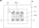
- FIG. 2 is a plan view of the core board, electronic components, and metal posts included in the board shown in FIG.
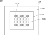
- FIG. 3 is a plan view schematically showing an example of a substrate according to an embodiment of the present invention, in which metal posts have different shapes when viewed from above.
- FIG. 4A is a perspective view schematically showing an example of a coaxial cable manufacturing process.
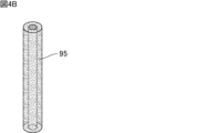
- FIG. 4B is a perspective view schematically showing an example of a coaxial cable manufacturing process.
- FIG. 4C is a perspective view schematically showing an example of a coaxial cable manufacturing process.
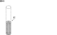
- FIG. 4D is a perspective view schematically showing an example of a coaxial cable manufacturing process.
- FIG. 4A is a perspective view schematically showing an example of a coaxial cable manufacturing process.
- FIG. 4B is a perspective view schematically showing an example of a coaxial cable manufacturing process.
- FIG. 5 is a plan view schematically showing an example of a board according to an embodiment of the present invention, in which a part of a metal post is a coaxial cable.
- FIG. 6 is a cross-sectional view schematically showing an example of a module according to an embodiment of the present invention.
- FIG. 7 is a plan view of the module shown in FIG. 6, showing the positional relationship between the heating element and each component of the board.
- FIG. 8 is a diagram schematically showing an example of a process of attaching an adhesive film for fixing electronic components to a core substrate.
- FIG. 9 is a cross-sectional view schematically showing an example of the process of arranging electronic components and metal posts on an adhesive film.
- FIG. 10 is a cross-sectional view schematically showing an example of the process of filling the opening of the core substrate with a sealing material.
- FIG. 11 is a cross-sectional view schematically showing an example of a process of grinding or polishing the sealing material and the metal post.
- FIG. 12 is a cross-sectional view schematically showing an example of the process of forming a via.
- FIG. 13 is a cross-sectional view schematically showing an example of the process of forming a wiring layer.
- FIG. 14 is a cross-sectional view schematically showing an example of the process of forming a buildup layer.
- the present invention is not limited to the following configuration, and can be modified and applied as appropriate without changing the gist of the present invention. Note that the present invention also includes a combination of two or more of the individual desirable configurations described below.
- FIG. 1 is a cross-sectional view schematically showing an example of a substrate according to an embodiment of the present invention.
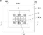
- FIG. 2 is a plan view of the core board, electronic components, and metal posts included in the board shown in FIG. Note that FIG. 1 is a cross-sectional view taken along the line XX shown in FIG. 2.
- the substrate 100 shown in FIGS. 1 and 2 has a first surface 11 and a second surface 12 opposite to the first surface 11, and has a core substrate 10 provided with an opening 13 inside. an electronic component 20 and a metal post 90 provided in the opening 13; a sealing material 30 that is filled in the opening 13 and has a third surface 31 on the first surface 11 side and a fourth surface 32 on the second surface 12 side; Equipped with
- first via conductor 40 is connected to the first electrode 21 of the electronic component 20 or the fifth surface 91 of the metal post 90, and the first via conductor 40 is connected to the second electrode 22 of the electronic component 20 or the sixth surface 92 of the metal post 90.
- the second via conductor 50 , the first buildup layer (rewiring layer) 60 provided in contact with the first surface 11 of the core substrate 10 and the third surface 31 of the sealing material 30 , and the second via conductor 50 of the core substrate 10 .
- a second buildup layer (rewiring layer) 70 provided in contact with the second surface 12 and the fourth surface 32 of the sealing material 30 is provided.
- the core substrate 10 a resin substrate, a glass substrate, a ceramic substrate, etc. can be used.
- the core substrate 10 may be a printed wiring board having conductor wiring provided on its surface or inside.
- an insulating support substrate (core material) formed from a resin such as epoxy resin and a reinforcing material such as glass cloth can be used.
- the supporting substrate may contain inorganic particles such as silica particles and alumina particles.
- the first surface 11 and second surface 12 of the core substrate 10 are parallel surfaces to each other, and constitute a pair of opposing main surfaces of the core substrate 10.
- the opening 13 of the core substrate 10 passes through the core substrate 10.
- the shape of the opening 13 when the core substrate 10 is viewed from above is not particularly limited, and in addition to the rectangle shown in FIG. You can.
- the substrate 100 is a component-embedded substrate in which an electronic component 20 is embedded. ing. A metal post 90 is housed in the same opening 13 where the electronic component 20 is housed.
- the electronic component 20 and the metal post 90 may be arranged two-dimensionally within the opening 13 as shown in FIG. 2, or may be arranged one-dimensionally within the opening 13. In the former case, the electronic components 20 and the metal posts 90 may be arranged, for example, in a matrix (FIG. 2) or in a staggered manner.
- the electronic component 20 is not particularly limited, and examples thereof include passive components such as a capacitor (for example, a multilayer ceramic capacitor (MLCC)) and an inductor.
- the electronic component 20 is a chip component having a longitudinal shape such as a rectangular parallelepiped shape or a cylindrical shape.
- the electronic components 20 of the same type are components of the same size as defined by the size notation of chip components.
- the size notation is a notation defined by JIS (Japanese Industrial Standards) and EIA (Electronic Industries Alliance), and examples of the size notation include 0603 and the like in JIS.
- the electronic components 20 of the same type may be components of the same type among the basic components of an electric circuit, such as capacitors or inductors.
- the electronic components 20 of the same type may be components having the same model among capacitors or inductors, for example.
- each electronic component 20 in the height direction (direction along the first direction D1 or second direction D2, which will be described later), which is the direction along the thickness direction of the core substrate 10, are It is preferable that the shape is larger than the dimensions in other directions orthogonal to the width direction. Thereby, the electronic components 20 can be arranged with higher density.
- the electronic component 20 has a first electrode 21 in a first direction D1 that is perpendicular to the second surface 12 of the core substrate 10 and toward the first surface 11 side, and has a first electrode 21 in a direction opposite to the first direction D1. It has a second electrode 22 in the second direction D2.
- the first electrode 21 and the second electrode 22 are located at one end and the other end in the longitudinal direction of the elongated electronic component 20, respectively.
- the sealing material 30 is a member for sealing the electronic component 20 and the metal post 90 within the opening 13, and is filled around the electronic component 20 and the metal post 90 within the opening 13.
- the sealing material 30 includes a resin such as an epoxy resin and a filler made of inorganic particles such as silica particles and alumina particles.
- the side surface of the metal post 90 is coated with an insulating resin, or an oxide film is formed on the side surface of the metal post 90. It may also be provided with insulation properties.
- the side surface of the metal post 90 is a surface other than the fifth surface 91 and the sixth surface 92 of the metal post 90, and is a surface that is not used for connection with other conductors.
- At least one first via conductor 40 is provided for each of the electronic component 20 and the metal post 90, and the electronic component 20 and the metal post 90 are connected to each other via the first via conductor 40. 1 buildup layer 60 .
- the first via conductor 40 connected to the electronic component 20 penetrates at least the insulating layer 61 of the first buildup layer 60 closest to the core substrate 10 and the third surface 31 of the sealing material 30, and conducts the corresponding electronic The first electrode 21 of the component 20 is reached.
- the first via conductor 40 connected to the metal post 90 at least penetrates the insulating layer 61 of the first buildup layer 60 closest to the core substrate 10, and the corresponding metal post 90 It reaches the fifth surface 91, which is the surface exposed from the surface 31.
- the second via conductor 50 connected to the electronic component 20 at least penetrates the insulating layer 71 of the second buildup layer 70 closest to the core substrate 10 and reaches the second electrode 22 of the corresponding electronic component 20 .
- the second via conductor 50 connected to the metal post 90 at least penetrates the insulating layer 71 of the second buildup layer 70 closest to the core substrate 10, and the corresponding metal post 90 It reaches the sixth surface 92, which is the surface exposed from the surface 32.
- the first buildup layer 60 electrically connects the electronic components 20 to each other, the metal posts 90 to each other, and the electronic components 20 and metal posts 90 to other components, through holes, terminals, etc., and includes at least one insulating layer. Layers 61 and at least one wiring layer 62 are alternately stacked.
- the second buildup layer 70 electrically connects the electronic components 20 to each other, the metal posts 90 to each other, and the electronic components 20 and metal posts 90 to other components, through holes, terminals, etc., and at least one Two insulating layers 71 and at least one wiring layer 72 are alternately stacked.
- the metal post 90 is exposed from the third surface 31 of the sealing material 30 and from the fourth surface 32 of the sealing material 30.
- the first via conductor 40 on the first surface 11 side of the core substrate 10 is connected to the fifth surface 91 of the metal post 90
- the second via conductor 40 on the second surface 12 side of the core substrate 10 is connected to the fifth surface 91 of the metal post 90.
- 50 is connected to the sixth surface 92 of the metal post 90, the first via conductor 40 and the second via conductor 50 are electrically connected via the metal post 90. That is, the metal post 90 enables conduction between the first surface 11 side and the second surface 12 side of the core substrate 10.
- the metal post 90 is a columnar conductor provided within the opening 13, by providing the metal post 90 within the opening 13, the wiring length can be made straight from directly above the opening 13 to directly below it. You can easily connect without any hassle. That is, there is no need to form wiring that detours around the opening 13.
- the fifth surface 91 of the metal post 90 is located on the same surface as the first surface 11 of the core substrate and the third surface 31 of the sealing material 30. 91 is exposed from the third surface 31 of the sealing material 30. In the substrate manufactured by the manufacturing process described later, the positional relationship of these surfaces is as described above. However, the position of the fifth surface 91 of the metal post 90 is not limited to this position, and may protrude from the third surface 31 of the sealing material 30 or may be depressed. In other words, the fifth surface 91 of the metal post 90 may be located above or below the third surface 31 of the sealing material 30 in FIG.
- the fact that the fifth surface 91 of the metal post 90 is exposed from the third surface 31 of the sealing material 30 means that the fifth surface 91 of the metal post 90 is not covered with the sealing material 30 which is an insulating layer. do. Further, it is preferable that the fifth surface 91 of the metal post 90 is directly connected to a conductor (first via conductor 40 in FIG. 1) located on the first surface 11 side of the core substrate 10. Further, a relatively thin insulator or a highly thermally conductive resin may be present between the fifth surface 91 of the metal post 90 and the conductor located on the first surface 11 side of the core substrate 10.
- the sixth surface 92 of the metal post 90 is located on the same surface as the second surface 12 of the core substrate and the fourth surface 32 of the sealant.
- the sixth surface 92 is exposed from the fourth surface 32 of the sealing material 30.
- the position of the sixth surface 92 of the metal post 90 is not limited to this position, and may protrude from the fourth surface 32 of the sealing material 30 or may be depressed. In other words, the position of the sixth surface 92 of the metal post 90 may be located lower or upper in FIG. 1 than the fourth surface 32 of the sealing material 30.
- the fact that the sixth surface 92 of the metal post 90 is exposed from the fourth surface 32 of the sealant 30 means that the sixth surface 92 of the metal post 90 is not covered with the sealant 30 which is an insulating layer. do. Further, it is preferable that the sixth surface 92 of the metal post 90 is directly connected to a conductor (second via conductor 50 in FIG. 1) located on the second surface 12 side of the core substrate 10. Further, a relatively thin insulator or a highly thermally conductive resin may be present between the sixth surface 92 of the metal post 90 and the conductor located on the second surface 12 side of the core substrate 10.
- the metal post 90 has a shape in which the dimension in the height direction, which is the direction along the thickness direction of the core substrate 10, is larger than the dimension in other directions perpendicular to the height direction. This shape can be said to be columnar, and the longitudinal direction of the columnar metal post 90 is along the thickness direction of the core substrate 10.
- the metal post 90 is made of a metal material, preferably copper or a copper alloy. Since the metal post 90 is made of a metal material, it has high conductivity, and can be electrically connected linearly from directly above to directly below the opening 13 with low electrical resistance. Since copper or copper alloy has a low volume resistivity as a material, it is possible to further reduce the electrical resistance. Moreover, the heat dissipation effect from directly above to directly below the opening 13 can be exhibited.
- FIG. 2 shows an electronic component 20 and a metal post 90 provided within the opening 13.
- the electronic components 20 and the metal posts 90 are arranged in a grid pattern, they may be arranged in a staggered pattern or in any other arrangement, and the arrangement pattern is not particularly limited.
- the distance between the metal post 90 and the wall surface 13a of the opening 13 is indicated by a double arrow S1
- the distance between the metal post 90 and the electronic component 20 closest to the metal post 90 is indicated by a double arrow S2.
- the distance S2 between the metal post 90 and the nearest electronic component 20 is preferably smaller than the distance S1 between the metal post 90 and the wall surface 13a of the opening 13.
- the distance S1 is determined by image analysis of a photograph of the substrate 100. More specifically, an enlarged photograph of a cross section parallel to the second surface 12 of the core substrate 10 was obtained using a scanning electron microscope (SEM) or a transmission electron microscope (TEM), and the metal post 90 and the wall surface of the opening 13 were observed. 13a, line segments are drawn on the opposing contours using image analysis software, and the average distance between the line segments is determined. Then, the distances between all the metal posts 90 and the wall surface 13a of the opening 13 are determined, and the average value is set as the distance S1.
- An X-ray photograph may be used instead of a photograph taken by a scanning electron microscope (SEM) or a transmission electron microscope (TEM).
- the distance S2 is determined by image analysis of a photograph of the substrate 100. More specifically, an enlarged photograph of a cross section parallel to the second surface 12 of the core substrate 10 is obtained using a scanning electron microscope (SEM) or a transmission electron microscope (TEM), and the electronic component 20 closest to the metal post 90 is shown. For each, line segments are drawn on opposing contour lines using image analysis software, and the average distance between the line segments is determined. Then, the distance between all the metal posts 90 and the nearest electronic component is determined, and the average value is set as the distance S2.
- An X-ray photograph may be used instead of a photograph taken by a scanning electron microscope (SEM) or a transmission electron microscope (TEM).
- an electronic component that generates heat during operation means a component that becomes hotter during operation than when not in operation.
- An example of the temperature of an electronic component during operation is a component whose temperature rises to about 100°C.
- the metal post 90 is made of a metal material, it has high thermal conductivity and is excellent in heat dissipation effect.
- the thermal conductivity of the material of the metal post 90 is preferably 100 W/mK or more, more preferably 300 W/mK or more.
- a plurality of electronic components 20 are provided within the opening 13.
- the distance between the central axis of the metal post 90 and the central axis of the electronic component 20 closest to the metal post 90 is indicated by a double arrow C1
- the distance between the central axes of the plurality of electronic components 20 is indicated by a double arrow C2.
- the distance C1 between the central axis of the metal post 90 and the central axis of the electronic component 20 closest to the metal post 90 is preferably approximately equal to the distance C2 between the central axes of the plurality of electronic components 20. .
- the term "approximately equidistant" here does not mean that the distance C1 and the distance C2 are completely the same; the lower limit of the distance C2 is 95% and the upper limit is 105% as relative values when the distance C1 is 100%. % range. Moreover, since the values of distance C1 and distance C2 can be measured at multiple locations within one opening, the average value thereof is used. When the electronic component 20 and the metal post 90 are arranged in the same opening 13 in the closest density, the relationship between the distance C1 and the distance C2 becomes this relationship. From the viewpoint of effectively using the space within the opening 13, it is preferable that there is little empty space within the opening 13 and that the electronic components 20 and the metal posts 90 are arranged in the closest density.
- the height dimension of the metal post 90 is indicated by a double arrow H90
- the height dimension of the electronic component 20 is indicated by a double arrow H20.
- the height dimension H90 of the metal post 90 along the thickness direction of the core substrate 10 is larger than the height dimension H20 of the electronic component 20. ing. This means that when the metal post 90 is provided in the opening 13 in the manufacturing process of the substrate 100, which will be described later, the upper end of the metal post 90 is ground or polished to form the first surface 11 of the core substrate 10 and the sealing material 30. This is due to the fact that a method of aligning the third surface 31 and the fifth surface 91 of the metal post 90 is adopted.
- the height dimension H20 of the electronic component 20 is smaller. It is preferable that the difference between the height dimension H90 of the metal post 90 and the height dimension H20 of the electronic component is, for example, 20 ⁇ m or more and 600 ⁇ m or less.
- the heights of the fifth surface 91 of the metal post 90 and the first surface 21 of the electronic component 20 vary, and the heights of the sixth surface 92 of the metal post 90 and the second surface 22 of the electronic component 20 vary.
- the heights are the same. Due to this, the fourth surface 32 of the sealant 30 is a flatter surface than the third surface 31 of the sealant 30. Fine wiring can be formed on the fourth surface 32 of the sealing material 30, which is a flatter surface. Therefore, the smallest line, which is the smallest width (line) of the wiring layer 72 provided on the fourth surface 32 of the sealing material 30, is the smallest line of the wiring layer 62 provided on the third surface 31 of the sealing material 30.
- the width is thinner than the smallest line, which is the smallest value among the wiring widths (lines).
- higher-definition vias and wiring can be formed on the fourth surface 32 of the sealing material 30, which is flatter than the third surface 31 of the sealing material 30.
- the interval between wires when multiple wires are lined up at equal intervals is called a space, but the minimum space between the wires in the wiring layer 72 is sometimes narrower than the minimum space between the wires in the wiring layer 62.
- Lines and spaces are collectively called line and space, and the thinner the line and space, the more precise the wiring. Since high-definition wiring can be formed by the wiring of the wiring layer 72, it is preferable that the minimum line and space of the wiring of the wiring layer 72 is thinner than the minimum line and space of the wiring of the wiring layer 62.
- the height of the metal post 90 may vary. There may be cases where the dimension H90 in the height direction and the dimension H20 in the height direction of the electronic component 20 are the same, or the dimension H90 in the height direction of the metal post 90 is smaller than the dimension H20 in the height direction of the electronic component 20. However, such cases are not excluded from the scope of the present invention.
- the cross section of the substrate 100 shown in FIG. 1 is a cross section perpendicular to the second surface 12 of the core substrate 10, and in this cross section, the metal post 90 is disposed between the wall surface 13a of the opening 13 and the electronic component 20. It is preferable that the linear expansion coefficient of the metal post 90 is between the linear expansion coefficient of the core substrate 10 and the linear expansion coefficient of the electronic component 20.
- the linear expansion coefficient of the resin material used as the core substrate is about 40 ppm/K
- the linear expansion coefficient of the multilayer ceramic capacitor, which is assumed to be used as an electronic component is about 10 ppm/K. Adds thermal stress.
- the coefficient of linear expansion of copper assumed to be the metal post 90 is about 16, which is between the coefficient of linear expansion of the core substrate 10 and the coefficient of linear expansion of the electronic component 20. Therefore, by arranging the metal post 90 between the wall surface 13a of the opening 13 and the electronic component 20, that is, between the core substrate 10 and the electronic component 20, the linear expansion coefficient of the core substrate 10 and the linear expansion of the electronic component 20 can be adjusted. It is possible to alleviate the influence of the difference in coefficients, alleviate the thermal stress applied between the core substrate 10 and the electronic component 20, and prevent defects such as cracks caused by thermal stress.
- the shapes and sizes of the electronic component 20 and the metal post 90 are drawn to be approximately the same, but they may be the same or different. By making the metal post 90 relatively large, the heat dissipation effect can be improved.
- the top view shape of the electronic component in a cross section parallel to the second surface, is rectangular, and the top view shape of the metal post is a shape obtained by chamfering the apex of a polygon that is more than a square, or a shape that is more than a pentagon. may be polygonal, circular, oval, oblong, or racetrack shaped. Further, the top view area of the metal post may be the same as or larger than the top view area of the electronic component.
- FIG. 3 is a plan view schematically showing an example of a substrate according to an embodiment of the present invention, in which metal posts have different shapes when viewed from above.
- FIG. 3 shows a substrate 101 including a metal post 93 having a circular shape when viewed from above. Further, in the substrate 101, the electronic component 20 has a rectangular shape when viewed from above, and its four corners are rounded (not chamfered).
- thermosetting resin and a filler are placed on the first surface 11 of the core substrate 10 under vacuum. Laminate uncured films. Thereafter, this film is heated and pressed to soften it, thereby filling the openings 13 with the thermosetting resin and filler.
- the top view shape of the electronic component 20 and the metal post 90 are all rectangular as shown in FIG. 2
- the top view shape of the metal post 93 is circular as shown in FIG. The fluidity of the softened resin in the vicinity of the metal post 93 is increased, and as a result, bubble clogging and filler clogging are suppressed, so that filling performance is improved.
- the metal post may have a coaxial cable shape in which the outer periphery of a metal wire is covered with a resin coating layer, and the outer periphery of the resin coating layer is covered with a metal coating layer.
- 4A, 4B, 4C, and 4D are perspective views schematically showing an example of a coaxial cable manufacturing process.
- FIG. 5 is a plan view schematically showing an example of a board according to an embodiment of the present invention, in which a part of a metal post is a coaxial cable.
- the outer periphery of the metal wire 94 shown in FIG. 4A is covered with a resin coating layer 95 shown in FIG. 4B, and the outer periphery of the resin coating layer 95 is covered with a metal coating layer 96 shown in FIG. 4C. It can be obtained by When using a coaxial cable as the metal post, cut the coaxial cable 97 so that its length is the same as or slightly longer than the thickness of the opening 13 (see FIG. 4D).
- Copper or a copper alloy is preferably used for the metal wire 94 and the metal coating layer 96.
- the resin coating layer 95 polyethylene, polytetrafluoroethylene (PTFE), tetrafluoroethylene/perfluoroalkyl vinyl ether copolymer resin (PFA), etc. are preferably used.
- the board 102 shown in FIG. 5 includes a metal post 90 made of metal and a metal post made of a coaxial cable 97.
- the coaxial cable 97 also enables conduction between the first surface 11 side and the second surface 12 side of the core board 10. Further, since the coaxial cable 97 has excellent high frequency characteristics, it can be used as wiring for high frequency signal transmission. Furthermore, since it is difficult in the manufacturing process to provide a through hole as a conductor that penetrates the core board 10 with a structure similar to that of a coaxial cable, it is possible to easily create a structure with excellent high frequency characteristics by placing the coaxial cable 97 in the opening 13. Wiring for vertical continuity can be provided.
- the board 102 shown in FIG. 5 includes both a metal post 90 made of metal and a metal post made of a coaxial cable 97, it may include only the coaxial cable 97 as the metal post. Further, the positional relationship and the ratio of the number of metal posts 90 made of metal and metal posts made of coaxial cable 97 are not particularly limited.
- the module of the present invention is a module in which a heating element is mounted on the first surface side of the core substrate of the substrate of the present invention, and the heating element and the metal post are seen from above in a plane parallel to the first surface.
- the positions of the heating element and the metal post overlap, and the heating element and the metal post are directly connected, or the heating element and the metal post are connected via a first material having a higher thermal conductivity than the sealing material.
- the area of the portion where the position of the metal post overlaps with respect to the area of the heating element is 10% or more and 100% or less.
- FIG. 6 is a cross-sectional view schematically showing an example of a module according to an embodiment of the present invention.
- FIG. 7 is a plan view of the module shown in FIG. 6, showing the positional relationship between the heating element and each component of the board. Note that FIG. 6 is a cross-sectional view of the substrate taken along the YY line (shown in FIG. 7), and in FIG. 7, the position of the heating element is added with a chain double-dashed line.
- a heating element 110 is mounted on the first surface 11 side (more precisely, on the first buildup layer 60) of the core substrate 10 of the substrate 100 shown in FIGS. 1 and 2. It is a module that has been developed.
- the heating element 110 examples include electronic components such as semiconductor components such as a CPU and memory, light emitting elements such as LEDs, and passive components such as inductors and capacitors.
- the heating element 110 is not particularly limited as long as it is a component that generates heat during use.
- the position where the heating element 110 is mounted is such that the position of the heating element 110 and the metal post 90 overlap when viewed from above in a plane parallel to the first surface 11. That is, it can be said that the metal post 90 is located directly below the heating element 110.
- the heat generated by the heating element 110 can be transmitted (radiated) to the second surface 12 side of the core substrate 10 via the metal post 90.
- the heat radiation path from the heating element 110 is shown by arrows in FIG. Further, the heating element 110 may be electrically connected to the metal post 90 located directly below it.
- the heating element and the metal post When the heating element and the metal post are electrically connected, the heating element and the metal post are directly connected, or the heating element and the metal post have a higher thermal conductivity than the sealing material.
- An example is a form in which the two are connected through one material.
- the form shown in FIG. 6 is the latter form, and can be said to be a form in which the first material is the first via conductor 40 and the wiring layer 62 of the first buildup layer 60.
- the first via conductor 40 and the wiring layer 62 are electrically conductive and are made of a material with higher thermal conductivity than the sealing material 30.
- the first material is preferably a metal material, more preferably copper or a copper alloy. Since the first material has a higher thermal conductivity than the sealing material 30, heat from the heating element 110 is efficiently transmitted to the metal post 90 via the first material.
- the thermal resistance in the path from the heating element to the fourth surface of the encapsulant via the third surface of the encapsulant and the metal post is It is preferable that the thermal resistance is lower than the thermal resistance of a route that does not go through the route and reaches the fourth surface of the sealing material.
- a second material having a higher thermal conductivity than the sealing material is provided on the second surface side of the core substrate, and that the metal post and the second material are connected.
- the second material corresponds to the second via conductor 50 and the wiring layer 72 of the second buildup layer 70.
- the metal post 90 and the second via conductor 50 are connected on the second surface 12 side of the core substrate 10, and the wiring layer 72 is further connected to the second via conductor 50. Since the second via conductor 50 and the wiring layer 72 are electrically conductive, when it is necessary to transmit an electrical signal from the heating element 110, they play the role of transmitting the signal to the second surface 12 side of the core board. be able to.
- the second via conductor 50 and the wiring layer 72 are made of a material with higher thermal conductivity than the sealing material 30, heat from the heating element 110 is transferred to the surface on which the heating element 110 is mounted via the second material. It can be transmitted to the opposite side.
- the second material is preferably a metal material, more preferably copper or a copper alloy.
- the module of the present invention may include, in addition to the heating element mounted on the first surface side of the core substrate, another heating element mounted on the second surface side. Further, the number of heating elements mounted on the core substrate may be one or more. If multiple heating elements are mounted, it is preferable that the positions of the heating elements and metal posts overlap when viewed from above in a plane parallel to the first surface of each heating element. Regarding the heating element, the positions of the heating element and the metal post do not need to overlap. If there is even one heating element in which the position of the heating element and the metal post overlap when viewed from above, it is included in the module of the present invention.
- the substrate of the present invention there is no distinction between the first and second surfaces of the core substrate, so if a heating element is mounted on either side of the substrate, the surface on which the heating element is mounted is used as the core. It is regarded as the first surface side of the substrate.
- FIG. 8 is a diagram schematically showing an example of a process of attaching an adhesive film for fixing electronic components to a core substrate.
- an opening 13 is formed in the core substrate 10, and an adhesive film 80 for fixing electronic components and metal posts is attached to the second surface 12 of the core substrate 10.
- FIG. 9 is a cross-sectional view schematically showing an example of the process of arranging electronic components and metal posts on an adhesive film.
- the electronic component 20 is placed on the adhesive film 80.
- the electronic component 20 is placed on the adhesive film 80 so that the first electrode 21 faces upward and the second electrode 22 faces downward.
- the second electrode 22 is attached to the adhesive film 80.
- a metal post 90 is also placed on the adhesive film 80. The height of the metal post 90 is set higher than the first electrode 21 of the electronic component 20 and the first surface 11 of the core substrate 10.
- FIG. 10 is a cross-sectional view schematically showing an example of the process of filling the opening of the core substrate with a sealing material.
- the electronic component 20 and metal post 90 are sealed with a sealant 30.
- a sealant 30 Specifically, an uncured film containing a thermosetting resin and a filler is laminated on the first surface 11 of the core substrate 10 under vacuum. Thereafter, this film is heated and pressed to soften it, thereby filling the inside of the opening 13 around the electronic component 20 and the metal post 90 with a thermosetting resin and filler.
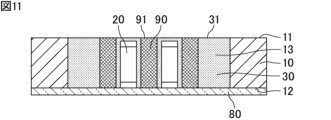
- FIG. 11 is a cross-sectional view schematically showing an example of the process of grinding or polishing the sealing material and the metal post.
- the sealing material 30 and metal post 90 are ground or polished on the first surface 11 side of the core substrate 10.
- the first surface 11 of the core substrate 10, the third surface 31 of the sealing material 30, and the fifth surface 91 of the metal post 90 are aligned.
- the fifth surface 91 of the metal post 90 is exposed from the third surface 31 of the sealing material 30.
- the first electrode 21 of the electronic component 20 is covered with the sealing material 30 and is not exposed. In this step, the electronic component 20 is not ground or polished.
- FIG. 12 is a cross-sectional view schematically showing an example of the process of forming a via.
- an insulating layer 61 is formed on the first surface 11 of the core substrate 10 and the third surface 31 of the sealing material 30.
- An insulating layer 71 is formed on the second surface 12 and the fourth surface 32 of the sealing material 30 (bottom in FIG. 12).
- the adhesive film 80 can also be used as it is without being peeled off.
- a via 82 is formed in the insulating layer 61 using a CO 2 laser or the like to expose the first electrode 21 of the electronic component 20 and the fifth surface 91 of the metal post 90, and a via 83 is formed in the insulating layer 71.
- the second electrode 22 of the electronic component 20 and the sixth surface 92 of the metal post 90 are exposed.
- the sealing material 30 covering the first electrode 21 of the electronic component 20 is also removed to form the via 82.
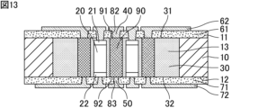
- FIG. 13 is a cross-sectional view schematically showing an example of the process of forming a wiring layer.
- plating for example, semi-additive method
- plating is used to fill the vias 82 and 83 to form the first via conductor 40 and the second via conductor 50, as well as the wiring layer 62 and the wiring layer.
- Form 72 is used to fill the vias 82 and 83 to form the first via conductor 40 and the second via conductor 50, as well as the wiring layer 62 and the wiring layer.
- FIG. 14 is a cross-sectional view schematically showing an example of the process of forming a buildup layer.
- layers are added as necessary to form the first buildup layer 60 and the second buildup layer 70.
- the substrate 100 can be manufactured.
- the fifth surface 91 of the metal post 90 is located at the same height as the third surface 31 of the encapsulant 30 and is exposed from the third surface 31 of the encapsulant 30. 1 via conductor 40.
- the sixth surface 92 of the metal post 90 is located at the same height as the fourth surface 32 of the encapsulant 30, is exposed from the fourth surface 32 of the encapsulant 30, and is connected to the second via conductor 50. .
- the height dimension of the metal post 90 becomes larger than the height dimension of the electronic component 20.
- a core substrate having a first surface and a second surface opposite to the first surface, and having an opening provided therein; an electronic component and a metal post provided in the same opening; a sealing material filled in the opening and having a third surface on the first surface side and a fourth surface on the second surface side, The metal post is exposed from the third surface of the sealing material and is exposed from the fourth surface of the sealing material.
- the metal post according to ⁇ 1> has a shape in which a dimension in a height direction, which is a direction along the thickness direction of the core substrate, is larger than a dimension in another direction orthogonal to the height direction. substrate.
- the electronic component is a component that generates heat during operation, and the distance between the metal post and the nearest electronic component is smaller than the distance between the metal post and the wall surface of the opening, ⁇ 1> or ⁇ 2>.
- ⁇ 4> A plurality of the electronic components are provided in the opening, In a cross section parallel to the second surface, the distance between the central axis of the metal post and the central axis of the electronic component closest to the metal post is approximately equal to the distance between the central axes of the plurality of electronic components.
- the metal post is one of ⁇ 1> to ⁇ 4>, wherein a dimension in the height direction along the thickness direction of the core board is larger than a dimension in the height direction of the electronic component.
- the coefficient of linear expansion of the metal post is between the coefficient of linear expansion of the core substrate and the coefficient of linear expansion of the electronic component,
- the electronic component has a rectangular top view shape, ⁇ 1> to ⁇ 6>, wherein the shape of the metal post when viewed from above is a polygon having a rectangular shape or more with rounded corners, a polygon having a pentagonal shape or more, a circle, an ellipse, an ellipse, or a racetrack shape.
- the substrate according to any one of the above.
- ⁇ 8> The board according to any one of ⁇ 1> to ⁇ 7>, wherein the metal post is made of copper or a copper alloy.
- the metal post is any one of ⁇ 1> to ⁇ 8>, wherein the outer periphery of the metal wire is coated with a resin coating layer, and the outer periphery of the resin coating layer is coated with a metal coating layer, and is in the shape of a coaxial cable.
- ⁇ 10> A module in which a heating element is mounted on the first surface side of the core substrate of the substrate according to any one of ⁇ 1> to ⁇ 9>, When viewed from above in a plane parallel to the first surface, the positions of the heating element and the metal post overlap, A module in which the heating element and the metal post are directly connected, or the heating element and the metal post are connected via a first material having a higher thermal conductivity than the sealing material.
- a second material having a higher thermal conductivity than the sealing material is provided on the second surface side of the core substrate, and the metal post and the second material are connected. module.
Landscapes
- Engineering & Computer Science (AREA)
- Microelectronics & Electronic Packaging (AREA)
- Manufacturing & Machinery (AREA)
- Production Of Multi-Layered Print Wiring Board (AREA)
- Casings For Electric Apparatus (AREA)
- Structures Or Materials For Encapsulating Or Coating Semiconductor Devices Or Solid State Devices (AREA)
Abstract
Description
しかしながら、本発明は、以下の構成に限定されるものではなく、本発明の要旨を変更しない範囲において適宜変更して適用することができる。なお、以下において記載する個々の望ましい構成を2つ以上組み合わせたものもまた本発明である。
図1は、本発明の実施形態に係る基板の一例を模式的に示す断面図である。図2は、図1に示す基板が備えるコア基板、電子部品及びメタルポストの平面図である。なお、図1は、図2に示すX-X線に沿った断面図である。
なお、メタルポスト90の側面は、メタルポスト90の第5面91及び第6面92以外の面であり、他の導体との接続に使用されない面である。
メタルポスト90の第5面91が封止材30の第3面31から露出するというのは、メタルポスト90の第5面91が絶縁層である封止材30に覆われていないことを意味する。
また、メタルポスト90の第5面91がコア基板10の第1面11側に位置する導体(図1では第1ビア導体40)に直接接続されていることが好ましい。
また、メタルポスト90の第5面91と、コア基板10の第1面11側に位置する導体との間に、比較的薄い絶縁体や高熱伝導性の樹脂が存在していてもよい。
メタルポスト90の第6面92が封止材30の第4面32から露出するというのは、メタルポスト90の第6面92が絶縁層である封止材30に覆われていないことを意味する。
また、メタルポスト90の第6面92がコア基板10の第2面12側に位置する導体(図1では第2ビア導体50)に直接接続されていることが好ましい。
また、メタルポスト90の第6面92と、コア基板10の第2面12側に位置する導体との間に、比較的薄い絶縁体や高熱伝導性の樹脂が存在していてもよい。
図2には開口部13内に設けられた電子部品20とメタルポスト90を示している。電子部品20とメタルポスト90は格子状に配置されているが、千鳥状に配置されてもよく、その他の配置でもよく、その配置のパターンは特に限定されない。
メタルポスト90の高さ方向の寸法H90と電子部品の高さ方向の寸法H20の差は、例えば20μm以上、600μm以下であることが好ましい。
より平坦な面である封止材30の第4面32には微細な配線を形成することができる。そのため、封止材30の第4面32に設ける配線層72の配線の幅(ライン)のうち最も小さい値である最小のラインは、封止材30の第3面31に設ける配線層62の配線の幅(ライン)のうち最も小さい値である最小のラインよりも細いことが好ましい。これにより、封止材30の第3面31に比べてより平坦な封止材30の第4面32側に、より高精細なビアや配線を形成することができる。
また、複数の配線が等間隔で並んでいる場合の配線と配線の間隔をスペースと呼ぶが、配線層72の配線の最小のスペースが、配線層62の配線の最小のスペースよりも細いことが好ましい。
ライン及びスペースを合わせてラインアンドスペースと呼び、ラインアンドスペースが細いと、より高精細な配線となる。配線層72の配線により高精細な配線を形成できることから、配線層72の配線の最小のラインアンドスペースが配線層62の配線の最小のラインアンドスペースより細いことが好ましい。
また、メタルポストの上面視面積が、電子部品の上面視面積と同じか大きくてもよい。
続いて、本発明の基板に発熱体が実装された本発明のモジュールについて説明する。
本発明のモジュールは、本発明の基板の、コア基板の第1面側に発熱体が実装されたモジュールであって、第1面と平行な面で見た上面視において、発熱体とメタルポストの位置が重なっており、発熱体とメタルポストが直接接続されている、又は、発熱体とメタルポストが封止材よりも熱伝導率が高い第1材料を介して接続されている。
また、第1面と平行な面で見た上面視において、発熱体の面積に対してメタルポストの位置が重なっている部分の面積が10%以上、100%以下であることが好ましい。
また、発熱体から封止材の第3面及びメタルポストを経由し封止材の第4面に至る経路における熱抵抗が、発熱体から封止材の第3面を経由し、メタルポストを経由せず封止材の第4面に至る経路の熱抵抗よりも小さいことが好ましい。
基板100は、以下の方法により製造することができる。図8は、コア基板に電子部品固定用の粘着フィルムを貼り付ける工程の一例を模式的に示す図である。
第1面及び前記第1面と反対側の第2面を有し、内部に開口部が設けられたコア基板と、
同じ前記開口部内に設けられた電子部品及びメタルポストと、
前記開口部内に充填され、前記第1面側の第3面及び前記第2面側の第4面を有する封止材と、を備え、
前記メタルポストは、前記封止材の前記第3面から露出し、かつ、前記封止材の第4面から露出する、基板。
前記メタルポストは、前記コア基板の厚さ方向に沿った方向である高さ方向の寸法が、前記高さ方向と直交する他の方向の寸法よりも大きい形状である、<1>に記載の基板。
前記電子部品は動作時に発熱する部品であり、前記メタルポストと前記開口部の壁面との距離よりも、前記メタルポストと最も近い前記電子部品との距離のほうが小さい、<1>又は<2>に記載の基板。
前記開口部に前記電子部品が複数設けられており、
前記第2面と平行な断面において、前記メタルポストの中心軸と、前記メタルポストに最も近い前記電子部品の中心軸との距離が、前記複数の電子部品の中心軸の間の距離と略等距離である、<1>から<3>のいずれか1つに記載の基板。
前記メタルポストは、前記コア基板の厚さ方向に沿った方向である高さ方向の寸法が、前記電子部品の高さ方向の寸法よりも大きい、<1>から<4>のいずれか1つに記載の基板。
前記メタルポストの線膨張係数は、前記コア基板の線膨張係数と前記電子部品の線膨張係数の間にあり、
前記第2面と直交する断面において、前記メタルポストは、前記開口部の壁面と前記電子部品との間に配置されている、<1>から<5>のいずれか1つに記載の基板。
前記第2面と平行な断面において、
前記電子部品の上面視形状が矩形状であり、
前記メタルポストの上面視形状が、四角形以上の多角形の頂点をR面取りした形状、五角形以上の多角形、円、楕円、長円、又はレーストラック形状である、<1>から<6>のいずれか1つに記載の基板。
前記メタルポストが銅又は銅合金である、<1>から<7>のいずれか1つに記載の基板。
前記メタルポストは、金属線の外周が樹脂被覆層で被覆され、前記樹脂被覆層の外周が金属被覆層で被覆された、同軸ケーブル形状である、<1>から<8>のいずれか1つに記載の基板。
<1>から<9>のいずれか1つに記載の基板の、前記コア基板の前記第1面側に発熱体が実装されたモジュールであって、
前記第1面と平行な面で見た上面視において、前記発熱体と前記メタルポストの位置が重なっており、
前記発熱体と前記メタルポストが直接接続されている、又は、前記発熱体と前記メタルポストが前記封止材よりも熱伝導率が高い第1材料を介して接続されている、モジュール。
前記第1材料は、金属材料である<10>に記載のモジュール。
前記コア基板における第2面側に、前記封止材よりも熱伝導率が高い第2材料が設けられ、前記メタルポストと前記第2材料が接続されている<10>又は<11>に記載のモジュール。
前記第2材料は、金属材料である<12>に記載のモジュール。
11 第1面
12 第2面
13 開口部
13a 開口部の壁面
20 電子部品
21 第1電極
22 第2電極
30 封止材
31 第3面
32 第4面
40 第1ビア導体
50 第2ビア導体
60 第1ビルドアップ層
61 絶縁層
62 配線層
70 第2ビルドアップ層
71 絶縁層
72 配線層
80 粘着フィルム
82、83 ビア
90、93 メタルポスト
91 第5面
92 第6面
94 金属線
95 樹脂被覆層
96 金属被覆層
97 同軸ケーブル
100、101、102 基板
110 発熱体
200 モジュール
C1 メタルポストの中心軸と電子部品の中心軸との距離
C2 複数の電子部品の中心軸間の距離
D1 第1方向
D2 第2方向
H20 電子部品の高さ
H90 メタルポストの高さ
S1 メタルポストと開口部の壁面との距離
S2 メタルポストと電子部品との距離
Claims (13)
- 第1面及び前記第1面と反対側の第2面を有し、内部に開口部が設けられたコア基板と、
同じ前記開口部内に設けられた電子部品及びメタルポストと、
前記開口部内に充填され、前記第1面側の第3面及び前記第2面側の第4面を有する封止材と、を備え、
前記メタルポストは、前記封止材の前記第3面から露出し、かつ、前記封止材の第4面から露出する、基板。 - 前記メタルポストは、前記コア基板の厚さ方向に沿った方向である高さ方向の寸法が、前記高さ方向と直交する他の方向の寸法よりも大きい形状である、請求項1に記載の基板。
- 前記電子部品は動作時に発熱する部品であり、前記メタルポストと前記開口部の壁面との距離よりも、前記メタルポストと最も近い前記電子部品との距離のほうが小さい、請求項1又は2に記載の基板。
- 前記開口部に前記電子部品が複数設けられており、
前記第2面と平行な断面において、前記メタルポストの中心軸と、前記メタルポストに最も近い前記電子部品の中心軸との距離が、複数の前記電子部品の中心軸の間の距離と略等距離である、請求項1~3のいずれかに記載の基板。 - 前記メタルポストは、前記コア基板の厚さ方向に沿った方向である高さ方向の寸法が、前記電子部品の高さ方向の寸法よりも大きい、請求項1~4のいずれかに記載の基板。
- 前記メタルポストの線膨張係数は、前記コア基板の線膨張係数と前記電子部品の線膨張係数の間にあり、
前記第2面と直交する断面において、前記メタルポストは、前記開口部の壁面と前記電子部品との間に配置されている、請求項1~5のいずれかに記載の基板。 - 前記第2面と平行な断面において、
前記電子部品の上面視形状が矩形状であり、
前記メタルポストの上面視形状が、四角形以上の多角形の頂点をR面取りした形状、五角形以上の多角形、円、楕円、長円、又はレーストラック形状である、請求項1~6のいずれかに記載の基板。 - 前記メタルポストが銅又は銅合金である、請求項1~7のいずれかに記載の基板。
- 前記メタルポストは、金属線の外周が樹脂被覆層で被覆され、前記樹脂被覆層の外周が金属被覆層で被覆された、同軸ケーブル形状である、請求項1~8のいずれかに記載の基板。
- 請求項1~9のいずれかに記載の基板の、前記コア基板の前記第1面側に発熱体が実装されたモジュールであって、
前記第1面と平行な面で見た上面視において、前記発熱体と前記メタルポストの位置が重なっており、
前記発熱体と前記メタルポストが直接接続されている、又は、前記発熱体と前記メタルポストが前記封止材よりも熱伝導率が高い第1材料を介して接続されている、モジュール。 - 前記第1材料は、金属材料である請求項10に記載のモジュール。
- 前記コア基板における第2面側に、前記封止材よりも熱伝導率が高い第2材料が設けられ、前記メタルポストと前記第2材料が接続されている請求項10又は11に記載のモジュール。
- 前記第2材料は、金属材料である請求項12に記載のモジュール。
Priority Applications (3)
| Application Number | Priority Date | Filing Date | Title |
|---|---|---|---|
| CN202380039088.5A CN119096707A (zh) | 2022-07-06 | 2023-02-27 | 基板以及模块 |
| JP2023569727A JP7662057B2 (ja) | 2022-07-06 | 2023-02-27 | 基板及びモジュール |
| US18/941,471 US20250071906A1 (en) | 2022-07-06 | 2024-11-08 | Substrate and module |
Applications Claiming Priority (2)
| Application Number | Priority Date | Filing Date | Title |
|---|---|---|---|
| JP2022109098 | 2022-07-06 | ||
| JP2022-109098 | 2022-07-06 |
Related Child Applications (1)
| Application Number | Title | Priority Date | Filing Date |
|---|---|---|---|
| US18/941,471 Continuation US20250071906A1 (en) | 2022-07-06 | 2024-11-08 | Substrate and module |
Publications (1)
| Publication Number | Publication Date |
|---|---|
| WO2024009554A1 true WO2024009554A1 (ja) | 2024-01-11 |
Family
ID=89452948
Family Applications (1)
| Application Number | Title | Priority Date | Filing Date |
|---|---|---|---|
| PCT/JP2023/006988 Ceased WO2024009554A1 (ja) | 2022-07-06 | 2023-02-27 | 基板及びモジュール |
Country Status (4)
| Country | Link |
|---|---|
| US (1) | US20250071906A1 (ja) |
| JP (1) | JP7662057B2 (ja) |
| CN (1) | CN119096707A (ja) |
| WO (1) | WO2024009554A1 (ja) |
Cited By (2)
| Publication number | Priority date | Publication date | Assignee | Title |
|---|---|---|---|---|
| WO2026009567A1 (ja) * | 2024-07-04 | 2026-01-08 | 株式会社村田製作所 | 電子部品集積モジュール、モジュール内蔵基板及び電子部品集積モジュールの製造方法 |
| WO2026075093A1 (ja) * | 2024-10-02 | 2026-04-09 | 株式会社村田製作所 | 電子部品内蔵基板 |
Families Citing this family (1)
| Publication number | Priority date | Publication date | Assignee | Title |
|---|---|---|---|---|
| TWI833522B (zh) * | 2022-12-23 | 2024-02-21 | 稜研科技股份有限公司 | 封裝結構 |
Citations (6)
| Publication number | Priority date | Publication date | Assignee | Title |
|---|---|---|---|---|
| JP2001291799A (ja) * | 2000-04-11 | 2001-10-19 | Ngk Spark Plug Co Ltd | 配線基板 |
| JP2005210074A (ja) * | 2003-12-26 | 2005-08-04 | Tdk Corp | 多層基板及びパワーアンプモジュール |
| JP2012023237A (ja) * | 2010-07-15 | 2012-02-02 | Nec Corp | 機能素子内蔵基板 |
| US20130027896A1 (en) * | 2011-07-29 | 2013-01-31 | Samsung Electro-Mechanics Co., Ltd. | Electronic component embedded printed circuit board and method of manufacturing the same |
| JP2014229908A (ja) * | 2013-05-24 | 2014-12-08 | サムソン エレクトロ−メカニックス カンパニーリミテッド. | 電子部品内臓印刷回路基板及びその製造方法 |
| WO2022124262A1 (ja) * | 2020-12-09 | 2022-06-16 | 株式会社村田製作所 | 高周波モジュール及び通信装置 |
-
2023
- 2023-02-27 WO PCT/JP2023/006988 patent/WO2024009554A1/ja not_active Ceased
- 2023-02-27 JP JP2023569727A patent/JP7662057B2/ja active Active
- 2023-02-27 CN CN202380039088.5A patent/CN119096707A/zh active Pending
-
2024
- 2024-11-08 US US18/941,471 patent/US20250071906A1/en active Pending
Patent Citations (6)
| Publication number | Priority date | Publication date | Assignee | Title |
|---|---|---|---|---|
| JP2001291799A (ja) * | 2000-04-11 | 2001-10-19 | Ngk Spark Plug Co Ltd | 配線基板 |
| JP2005210074A (ja) * | 2003-12-26 | 2005-08-04 | Tdk Corp | 多層基板及びパワーアンプモジュール |
| JP2012023237A (ja) * | 2010-07-15 | 2012-02-02 | Nec Corp | 機能素子内蔵基板 |
| US20130027896A1 (en) * | 2011-07-29 | 2013-01-31 | Samsung Electro-Mechanics Co., Ltd. | Electronic component embedded printed circuit board and method of manufacturing the same |
| JP2014229908A (ja) * | 2013-05-24 | 2014-12-08 | サムソン エレクトロ−メカニックス カンパニーリミテッド. | 電子部品内臓印刷回路基板及びその製造方法 |
| WO2022124262A1 (ja) * | 2020-12-09 | 2022-06-16 | 株式会社村田製作所 | 高周波モジュール及び通信装置 |
Cited By (2)
| Publication number | Priority date | Publication date | Assignee | Title |
|---|---|---|---|---|
| WO2026009567A1 (ja) * | 2024-07-04 | 2026-01-08 | 株式会社村田製作所 | 電子部品集積モジュール、モジュール内蔵基板及び電子部品集積モジュールの製造方法 |
| WO2026075093A1 (ja) * | 2024-10-02 | 2026-04-09 | 株式会社村田製作所 | 電子部品内蔵基板 |
Also Published As
| Publication number | Publication date |
|---|---|
| JP7662057B2 (ja) | 2025-04-15 |
| JPWO2024009554A1 (ja) | 2024-01-11 |
| CN119096707A (zh) | 2024-12-06 |
| US20250071906A1 (en) | 2025-02-27 |
Similar Documents
| Publication | Publication Date | Title |
|---|---|---|
| JP7662057B2 (ja) | 基板及びモジュール | |
| CN101742813B (zh) | 安装板和半导体模块 | |
| US7298047B2 (en) | Electronic circuit device | |
| CN102986313B (zh) | 部件内置布线基板 | |
| TW201630496A (zh) | 具有散熱結構的電路板及其製作方法 | |
| WO2017131017A1 (ja) | インダクタ部品およびその製造方法 | |
| JP7537637B2 (ja) | 基板 | |
| JPWO2011102134A1 (ja) | 部品内蔵基板 | |
| CN111901987A (zh) | 内嵌导热体的电路板及其制备方法 | |
| CN103907180B (zh) | 布线基板 | |
| JP2021005674A (ja) | 電子部品モジュール、電子部品ユニット、および、電子部品モジュールの製造方法 | |
| CN105576104A (zh) | 芯片衬底和芯片封装模块 | |
| CN113169143B (zh) | 半导体封装结构及其封装方法 | |
| JP2017005232A (ja) | 電子部品内蔵型配線基板 | |
| JP7645399B2 (ja) | 配線基板 | |
| CN101069283A (zh) | 封装的热能管理装置以及制造这种装置的方法 | |
| WO2024004261A1 (ja) | 基板 | |
| US20180332709A1 (en) | Inductor component and method of manufacturing inductor component | |
| CN104604341B (zh) | 布线基板及其制造方法 | |
| JP2795063B2 (ja) | 混成集積回路装置 | |
| CN118119082A (zh) | 内埋元件电路板及其制造方法 | |
| JP5933271B2 (ja) | 配線板、電子ユニット及び配線板の製造方法 | |
| US20250089167A1 (en) | Wiring substrate | |
| JP7133329B2 (ja) | 配線基板 | |
| JP2014044979A (ja) | 配線基板 |
Legal Events
| Date | Code | Title | Description |
|---|---|---|---|
| WWE | Wipo information: entry into national phase |
Ref document number: 2023569727 Country of ref document: JP |
|
| 121 | Ep: the epo has been informed by wipo that ep was designated in this application |
Ref document number: 23835095 Country of ref document: EP Kind code of ref document: A1 |
|
| WWE | Wipo information: entry into national phase |
Ref document number: 202380039088.5 Country of ref document: CN |
|
| NENP | Non-entry into the national phase |
Ref country code: DE |
|
| 122 | Ep: pct application non-entry in european phase |
Ref document number: 23835095 Country of ref document: EP Kind code of ref document: A1 |