WO2024004126A1 - 磁壁移動素子及び磁気アレイ - Google Patents
磁壁移動素子及び磁気アレイ Download PDFInfo
- Publication number
- WO2024004126A1 WO2024004126A1 PCT/JP2022/026190 JP2022026190W WO2024004126A1 WO 2024004126 A1 WO2024004126 A1 WO 2024004126A1 JP 2022026190 W JP2022026190 W JP 2022026190W WO 2024004126 A1 WO2024004126 A1 WO 2024004126A1
- Authority
- WO
- WIPO (PCT)
- Prior art keywords
- domain wall
- layer
- active region
- gate
- magnetoresistive element
- Prior art date
- Legal status (The legal status is an assumption and is not a legal conclusion. Google has not performed a legal analysis and makes no representation as to the accuracy of the status listed.)
- Ceased
Links
Images






Classifications
-
- H—ELECTRICITY
- H10—SEMICONDUCTOR DEVICES; ELECTRIC SOLID-STATE DEVICES NOT OTHERWISE PROVIDED FOR
- H10B—ELECTRONIC MEMORY DEVICES
- H10B61/00—Magnetic memory devices, e.g. magnetoresistive RAM [MRAM] devices
- H10B61/20—Magnetic memory devices, e.g. magnetoresistive RAM [MRAM] devices comprising components having three or more electrodes, e.g. transistors
-
- G—PHYSICS
- G11—INFORMATION STORAGE
- G11C—STATIC STORES
- G11C11/00—Digital stores characterised by the use of particular electric or magnetic storage elements; Storage elements therefor
- G11C11/02—Digital stores characterised by the use of particular electric or magnetic storage elements; Storage elements therefor using magnetic elements
- G11C11/16—Digital stores characterised by the use of particular electric or magnetic storage elements; Storage elements therefor using magnetic elements using elements in which the storage effect is based on magnetic spin effect
-
- H—ELECTRICITY
- H10—SEMICONDUCTOR DEVICES; ELECTRIC SOLID-STATE DEVICES NOT OTHERWISE PROVIDED FOR
- H10D—INORGANIC ELECTRIC SEMICONDUCTOR DEVICES
- H10D48/00—Individual devices not covered by groups H10D1/00 - H10D44/00
- H10D48/40—Devices controlled by magnetic fields
-
- H—ELECTRICITY
- H10—SEMICONDUCTOR DEVICES; ELECTRIC SOLID-STATE DEVICES NOT OTHERWISE PROVIDED FOR
- H10D—INORGANIC ELECTRIC SEMICONDUCTOR DEVICES
- H10D84/00—Integrated devices formed in or on semiconductor substrates that comprise only semiconducting layers, e.g. on Si wafers or on GaAs-on-Si wafers
- H10D84/80—Integrated devices formed in or on semiconductor substrates that comprise only semiconducting layers, e.g. on Si wafers or on GaAs-on-Si wafers characterised by the integration of at least one component covered by groups H10D12/00 or H10D30/00, e.g. integration of IGFETs
-
- H—ELECTRICITY
- H10—SEMICONDUCTOR DEVICES; ELECTRIC SOLID-STATE DEVICES NOT OTHERWISE PROVIDED FOR
- H10N—ELECTRIC SOLID-STATE DEVICES NOT OTHERWISE PROVIDED FOR
- H10N50/00—Galvanomagnetic devices
- H10N50/10—Magnetoresistive devices
Definitions
- the present invention relates to a domain wall displacement element and a magnetic array.
- a magnetoresistive element that utilizes a change in resistance value (change in magnetoresistance) based on a change in the relative angle of magnetization of two ferromagnetic layers.
- Patent Document 1 discloses a domain wall displacement type magnetoresistive element.
- a domain wall displacement type magnetoresistive element changes the resistance value in the stacking direction depending on the position of the domain wall, and can record data in multi-value or analog form.
- Domain wall displacement type magnetoresistive elements can be used in neuromorphic devices that imitate brain functions, as described in Patent Document 2, for example.
- a magnetoresistive element is often used as a magnetic array that integrates multiple elements. In order to process a large amount of information in a small area, magnetic arrays are required to be highly integrated.
- a domain wall displacement type magnetoresistive element can express more states as the domain wall moves over a wider range. In order to widen the movement range of the domain wall, the shape of the magnetoresistive element becomes longer in one direction.
- the write current is larger than the read current. In order to ensure a sufficient amount of write current, it is necessary to use a transistor with a large rated current, which increases the gate width of the transistor. That is, there are restrictions on the shape and size of both the magnetoresistive elements and the transistors that make up the magnetic array.
- the present invention has been made in view of the above problems, and an object of the present invention is to provide a domain wall displacement element and a magnetic array that can be highly integrated.
- a domain wall displacement element includes a first magnetoresistive element and a first transistor.
- the first magnetoresistive element includes a first domain wall motion layer, a first ferromagnetic layer, and a first nonmagnetic layer sandwiched between the first domain wall motion layer and the first ferromagnetic layer.
- the first transistor includes a first active region, a second active region, and a first gate that controls current between the first active region and the second active region.
- the first domain wall displacement layer is electrically connected to the first active region.
- the first magnetoresistive element has a length in a first direction that is longer than a length in a second direction orthogonal to the first direction.
- the first gate has a length in the first direction that is longer than a length in the second direction.
- the length of the first magnetoresistive element in the first direction is longer than the length of the first gate in the first direction.
- a first gate length direction connecting the first active region and the second active region intersects the first direction.
- the domain wall displacement element may further include a second magnetoresistive element.
- the second magnetoresistive element includes a second domain wall displacement layer, a second ferromagnetic layer, and a second nonmagnetic layer sandwiched between the second domain wall displacement layer and the second ferromagnetic layer.
- the first transistor further includes a third active region and a second gate that controls current between the second active region and the third active region.
- the second domain wall displacement layer is electrically connected to the third active region.
- the domain wall motion element according to the above aspect may further include a second transistor.
- the second transistor includes a fourth active region, a fifth active region, a sixth active region, a third gate that controls a current between the fourth active region and the fifth active region, and a third gate that controls a current between the fourth active region and the fifth active region. and a fourth gate that controls current between the fifth active region and the sixth active region.
- the fourth active region is electrically connected to the first domain wall displacement layer.
- the sixth active region is electrically connected to the second domain wall displacement layer.
- the domain wall motion element may further include a second transistor and a third magnetoresistive element.
- the second transistor includes a fourth active region, a fifth active region, a sixth active region, a third gate that controls a current between the fourth active region and the fifth active region, and a third gate that controls a current between the fourth active region and the fifth active region. and a fourth gate that controls current between the fifth active region and the sixth active region.
- the third magnetoresistive element includes a third domain wall displacement layer, a third ferromagnetic layer, and a third nonmagnetic layer sandwiched between the third domain wall displacement layer and the third ferromagnetic layer. have The fourth active region is electrically connected to the second domain wall displacement layer.
- the sixth active region is electrically connected to the third domain wall displacement layer.
- the domain wall displacement element according to the above aspect may further include a substrate.
- the first ferromagnetic layer may be closer to the substrate than the first domain wall displacement layer.
- a first conductive layer electrically connected to the first active region may be connected to an upper surface of the first domain wall displacement layer.
- the domain wall motion element In the domain wall motion element according to the above aspect, at least a portion of the first active region does not need to overlap with the first domain wall motion layer when viewed from the stacking direction.
- the domain wall motion element according to the above aspect may further include a second transistor.
- the second transistor includes a fourth active region, a fifth active region, and a third gate that controls current between the fourth active region and the fifth active region.
- the third gate has a length in the first direction that is longer than a length in the second direction. The length of the first magnetoresistive element in the first direction is shorter than the sum of the lengths of the first gate and the third gate in the first direction.
- the first channel between the first active region and the second active region is one selected from the group consisting of In, Ga, Zn, and Al. It may also contain oxides containing the above elements.
- the domain wall displacement element according to the above aspect may further include a second magnetoresistive element.
- the second magnetoresistive element includes a second domain wall displacement layer, a second ferromagnetic layer, and a second nonmagnetic layer sandwiched between the second domain wall displacement layer and the second ferromagnetic layer. have The first magnetoresistive element and the second magnetoresistive element may be located at different positions in the stacking direction.
- the domain wall displacement element according to the above aspect may further include a second magnetoresistive element.
- the second magnetoresistive element includes a second domain wall displacement layer, a second ferromagnetic layer, and a second nonmagnetic layer sandwiched between the second domain wall displacement layer and the second ferromagnetic layer. have At least one of the transistors connected to the first magnetoresistive element or the second magnetoresistive element may have a channel connecting two active regions formed in a stacking direction.
- a magnetic array according to a second aspect includes the domain wall displacement element according to the above aspect.
- the domain wall displacement element and magnetic array according to the above embodiments have excellent integration properties.
- FIG. 2 is a block diagram of a magnetic array according to the first embodiment.
- FIG. 3 is a circuit diagram of an integrated region of the magnetic array according to the first embodiment.
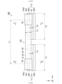
- FIG. 2 is a plan view of the domain wall displacement element according to the first embodiment.
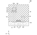
- FIG. 2 is a cross-sectional view of the domain wall displacement element according to the first embodiment.
- FIG. 1 is a cross-sectional view of a magnetoresistive element according to a first embodiment.
- FIG. 2 is a cross-sectional view of the domain wall displacement element according to the first embodiment.
- FIG. 2 is a cross-sectional view of the domain wall displacement element according to the first embodiment.
- FIG. 7 is a plan view of a domain wall displacement element according to a second embodiment.
- FIG. 7 is a plan view of a domain wall displacement element according to a third embodiment.
- FIG. 7 is a cross-sectional view of a domain wall displacement element according to a third embodiment.
- FIG. 7 is a cross-sectional view of a domain wall displacement element according to a third embodiment.
- FIG. 7 is a plan view of a domain wall displacement element according to a fourth embodiment.
- FIG. 7 is a plan view of a domain wall displacement element according to a fifth embodiment.
- FIG. 7 is a cross-sectional view of a domain wall displacement element according to a fifth embodiment.
- FIG. 7 is a cross-sectional view of a domain wall displacement element according to a sixth embodiment.
- FIG. 7 is a cross-sectional view of a domain wall displacement element according to a seventh embodiment.
- the x direction and the y direction are directions substantially parallel to one surface of a substrate Sub (see FIG. 4), which will be described later.
- the x direction is the longitudinal direction of the domain wall displacement layer 10, which will be described later, and may be referred to as a first direction.
- the y direction is a direction perpendicular to the x direction.
- the y direction may be referred to as a second direction.
- the z direction is a direction from the substrate Sub to the magnetoresistive element 100, which will be described later.
- the z direction is sometimes referred to as the stacking direction.
- the +z direction is sometimes expressed as "up” and the -z direction as "down”, but these expressions are for convenience and do not define the direction of gravity.
- "to connect” is not limited to the case of direct connection, but also includes the case of connection via another object in between.
- FIG. 1 is a block diagram of the magnetic array MA according to the first embodiment.
- Magnetic array MA has an integration area 1 and a peripheral area 2.
- the magnetic array MA can be used for, for example, a magnetic memory, a product-sum operator, a neuromorphic device, a spin memristor, and a magneto-optical element.
- the integration region 1 is an area in which a plurality of domain wall motion elements are integrated.
- the domain wall displacement element includes a magnetoresistive element and a transistor connected to the magnetoresistive element.
- the peripheral region 2 is a region in which a control element that controls the operation of the domain wall displacement element within the integrated region 1 is mounted.
- the peripheral region 2 includes, for example, a pulse application device 3, a resistance detection device 4, and an output section 5.
- the pulse application device 3 is configured to be able to apply a pulse to at least one of the plurality of domain wall displacement elements in the integrated region 1.
- the pulse application device 3 includes, for example, a control section 6 and a power source 7.
- the control unit 6 includes, for example, a processor and a memory.
- the processor is, for example, a CPU (Central Processing Unit).
- the processor operates based on an operating program stored in memory.
- the control unit 6 controls, for example, the address of the domain wall displacement element to which the pulse is applied, the magnitude (voltage, pulse length) of the pulse applied to a predetermined domain wall displacement element, and the like.
- the control unit 6 may also include a clock, a counter, a random number generator, and the like.
- the clock serves as an indicator of the timing of applying a pulse, and the counter counts the number of times the pulse is applied.
- the power supply 7 applies pulses to the domain wall displacement element according to instructions from the control unit 6.
- the resistance detection device 4 is configured to be able to detect the resistance value of the magnetoresistive element within the integrated region 1.
- the resistance detection device 4 may detect the resistance of each magnetoresistive element in the integrated region 1, or may detect the total resistance of the magnetoresistive elements belonging to the same column, for example.
- the resistance detection device 4 includes, for example, a comparator that compares the magnitude of the detected resistance values.
- the comparator may, for example, compare the detected resistance values with each other, or may compare the detected resistance value with a reference resistance value set in advance.
- the output section 5 is connected to the resistance detection device 4.
- the output unit 5 includes, for example, a processor, an output capacitor, an amplifier, a converter, and the like.
- the output unit 5 may perform an operation of substituting the detection result of the resistance detection device 4 into the activation function. The calculation is performed by a processor, for example.
- the output unit 5 outputs the calculation result to the outside.
- operations such as outputting the calculation result as an input signal to another magnetic array, or outputting it to the outside as a discrimination rate may be performed. It's okay. Further, the output unit 5 may feed back the calculation result to the pulse application device 3.
- FIG. 2 is a circuit diagram of the integrated region 1 according to the first embodiment.
- the integrated region 1 includes a plurality of domain wall displacement elements 200, a plurality of first wirings WL, a plurality of second wirings CL, and a plurality of third wirings RL.
- Each domain wall displacement element 200 includes a magnetoresistive element 100, a first transistor Tr1, and a second transistor Tr2.
- the third transistor Tr3 belongs to the pulse application device 3 of the peripheral region 2, for example.
- the plurality of domain wall displacement elements 200 are arranged, for example, in a matrix.
- the plurality of domain wall moving elements 200 are not limited to those in which actual elements are arranged in a matrix, but may be arranged in a matrix in a circuit diagram.
- Each of the first wirings WL is, for example, a write wiring. Each of the first wirings WL electrically connects the pulse application device 3 and one or more magnetoresistive elements 100.
- Each of the second wirings CL is, for example, a common wiring that can be used for both writing and reading data. Each of the second wirings CL is connected to the resistance detection device 4, for example. The second wiring CL may be provided in each of the plurality of magnetoresistive elements 100, or may be provided across the plurality of magnetoresistive elements 100.
- Each of the third wirings RL is, for example, a readout wiring. The third wiring RL electrically connects the pulse application device 3 and one or more magnetoresistive elements 100, respectively.
- the first transistor Tr1, the second transistor Tr2, and the third transistor Tr3 are elements that control the flow of current.
- the first transistor Tr1 is a field effect transistor.
- the second transistor Tr2 and the third transistor Tr3 may be field effect transistors or other elements that control current flow.
- Other devices that control current flow include devices that utilize phase changes in crystal layers, such as Ovonic Threshold Switches (OTS), and devices that utilize a band structure, such as metal-insulator transition (MIT) switches. These are elements that utilize change in conductivity, elements that utilize breakdown voltage such as Zener diodes and avalanche diodes, and elements that change conductivity as the atomic position changes.
- OTS Ovonic Threshold Switches
- MIT metal-insulator transition
- the first transistor Tr1 and the second transistor Tr2 are connected to each magnetoresistive element 100 one by one.
- the first transistor Tr1 is connected, for example, between the magnetoresistive element 100 and the first wiring WL.
- the second transistor Tr2 is connected, for example, between the magnetoresistive element 100 and the second wiring CL.
- the third transistor Tr3 is connected across the plurality of magnetoresistive elements 100, for example.
- the third transistor Tr3 is connected to, for example, the third wiring RL.
- the positional relationship between the second transistor Tr2 and the third transistor Tr3 is not limited to that shown in FIG. 2.
- the second transistor Tr2 may be connected across the plurality of magnetoresistive elements 100 and may be connected to one end of the second wiring CL.
- one third transistor Tr3 may be connected to each magnetoresistive element 100.
- FIG. 3 is a plan view of the domain wall displacement element 200 according to the first embodiment.
- FIG. 4 is a cross-sectional view of the domain wall displacement element 200 according to the first embodiment.
- FIG. 4 is a cross-sectional view taken along line AA in FIG.
- the domain wall displacement element 200 includes a magnetoresistive element 100, a first transistor Tr1, and a second transistor Tr2.
- the magnetoresistive element 100 and the first transistor Tr1 are electrically connected via the vertical wiring Vw1 and the in-plane wiring IPw1.
- the magnetoresistive element 100 and the second transistor Tr2 are electrically connected via the vertical wiring Vw2 and the in-plane wiring IPw2.
- the vertical wiring Vw1 and the vertical wiring Vw2 are wirings extending in the z direction.
- the in-plane wiring IPw1 and the in-plane wiring IPw2 are wirings extending in any direction within the xy plane.
- the vertical wiring Vw1, the vertical wiring Vw2, the in-plane wiring IPw1, and the in-plane wiring IPw2 are conductors.
- the periphery of the magnetoresistive element 100 is covered with an insulating layer 90.
- the insulating layer 90 is an insulating layer that insulates between wires of multilayer wiring and between elements.
- the insulating layer 90 is made of, for example, silicon oxide (SiO x ), silicon nitride (SiN x ), silicon carbide (SiC), chromium nitride, silicon carbonitride (SiCN), silicon oxynitride (SiON), or aluminum oxide (Al 2 O). 3 ), zirconium oxide (ZrO x ), etc.
- FIG. 5 is a cross-sectional view of the magnetoresistive element 100 according to the first embodiment.
- FIG. 5 is a cross-sectional view taken along line AA in FIG.
- the arrow shown in the figure is an example of the orientation direction of magnetization of the ferromagnetic material.
- the magnetoresistive element 100 includes, for example, a domain wall displacement layer 10, a nonmagnetic layer 20, a ferromagnetic layer 30, a first conductive layer 40, a second conductive layer 50, and a third conductive layer 60.
- the length L1 of the magnetoresistive element 100 in the x direction is longer than the length L2 in the y direction (see FIG. 3).
- the length of the magnetoresistive element is defined as the length of the portion where the first ferromagnetic layer, nonmagnetic layer, and ferromagnetic layer overlap when viewed from the z direction.
- the length of the domain wall displacement layer 10 in the x direction is longer than the length in the y direction.
- the domain wall displacement layer 10 has a plurality of magnetic domains therein, and a domain wall DW at the boundary between the plurality of magnetic domains.
- the domain wall displacement layer 10 is, for example, a layer in which information can be magnetically recorded by changing the magnetic state.
- the domain wall displacement layer 10 is also called an analog layer or a magnetic recording layer.
- the domain wall displacement layer 10 has a first region A1, a second region A2, and a third region A3.
- the first region A1 is a region that overlaps with the first conductive layer 40 when viewed from the z direction.
- the second region A2 is a region that overlaps with the second conductive layer 50 when viewed from the z direction.
- the third region A3 is a region other than the first region A1 and the second region A2 of the domain wall displacement layer 10.
- the third area A3 is, for example, sandwiched between the first area A1 and the second area A2 in the x direction.
- the magnetization M A1 of the first region A1 is fixed by the first conductive layer 40 .
- the magnetization M A2 of the second region A2 is fixed by the second conductive layer 50.
- Fixed magnetization means that the magnetization is not reversed during normal operation of the magnetoresistive element 100 (no unexpected external force is applied).
- the magnetization M A1 of the first region A1 and the magnetization M A2 of the second region A2 are, for example, oriented in opposite directions.
- the third region A3 is a region where the direction of magnetization changes and the domain wall DW can move.
- the third area A3 is called a domain wall movable area.
- the third region A3 has a first magnetic domain A31 and a second magnetic domain A32.
- the first magnetic domain A31 and the second magnetic domain A32 have opposite magnetization directions.
- the boundary between the first magnetic domain A31 and the second magnetic domain A32 is a domain wall DW.
- the magnetization M A31 of the first magnetic domain A31 is oriented in the same direction as the magnetization M A1 of the first region A1.
- the magnetization M A32 of the second magnetic domain A32 is, for example, oriented in the same direction as the magnetization M A2 of the adjacent second region A2.
- the domain wall DW moves within the third area A3 and does not invade the first area A1 and the second area A2.
- the domain wall DW moves.
- the domain wall DW is moved by passing a write current in the x direction in the third region A3, applying an external magnetic field to the third region A3, and the like.
- a write current for example, a current pulse
- electrons flow in the -x direction opposite to the current, so the domain wall DW moves in the -x direction.
- the spin-polarized electrons in the second magnetic domain A32 reverse the magnetization M A31 of the first magnetic domain A31.
- the domain wall DW moves in the -x direction.
- the domain wall displacement layer 10 is made of a magnetic material.
- the domain wall motion layer 10 may be a ferromagnetic material, a ferrimagnetic material, or a combination of these and an antiferromagnetic material whose magnetic state can be changed by an electric current.
- the domain wall displacement layer 10 preferably contains at least one element selected from the group consisting of Co, Ni, Fe, Pt, Pd, Gd, Tb, Mn, Ge, and Ga.
- Examples of materials used for the domain wall displacement layer 10 include a laminated film of Co and Ni, a laminated film of Co and Pt, a laminated film of Co and Pd, a MnGa-based material, a GdCo-based material, and a TbCo-based material.
- Ferrimagnetic materials such as MnGa-based materials, GdCo-based materials, and TbCo-based materials have small saturation magnetization, and the threshold current required to move the domain wall DW becomes small. Further, a laminated film of Co and Ni, a laminated film of Co and Pt, and a laminated film of Co and Pd have a large coercive force, and the moving speed of the domain wall DW becomes slow.
- the antiferromagnetic material include Mn 3 X (X is Sn, Ge, Ga, Pt, Ir, etc.), CuMnAs, Mn 2 Au, and the like. The same material as the ferromagnetic layer 30 described later can also be applied to the domain wall displacement layer 10.
- the nonmagnetic layer 20 is located between the domain wall displacement layer 10 and the ferromagnetic layer 30.
- the nonmagnetic layer 20 is laminated on one surface of the ferromagnetic layer 30.
- the nonmagnetic layer 20 is made of, for example, a nonmagnetic insulator, semiconductor, or metal.
- Nonmagnetic insulators are, for example, Al 2 O 3 , SiO 2 , MgO, MgAl 2 O 4 , and materials in which a portion of Al, Si, and Mg is replaced with Zn, Be, or the like. These materials have a large band gap and excellent insulating properties.
- the nonmagnetic layer 20 is made of a nonmagnetic insulator, the nonmagnetic layer 20 is a tunnel barrier layer.
- the nonmagnetic metal include Cu, Au, and Ag.
- Examples of the nonmagnetic semiconductor include Si, Ge, CuInSe 2 , CuGaSe 2 , and Cu(In,Ga)Se 2 .
- the thickness of the nonmagnetic layer 20 is, for example, 20 ⁇ or more, and may be 25 ⁇ or more.
- the resistance area product (RA) of the magnetoresistive element 100 becomes large.
- the resistance area product (RA) of the magnetoresistive element 100 is preferably 1 ⁇ 10 4 ⁇ m 2 or more, more preferably 5 ⁇ 10 4 ⁇ m 2 or more.
- the resistance area product (RA) of the magnetoresistive element 100 is the element resistance of one magnetoresistive element 100 and the element cross-sectional area of the magnetoresistive element (the area of the cross section of the nonmagnetic layer 20 cut along the xy plane). It is expressed as a product.
- the ferromagnetic layer 30 and the domain wall displacement layer 10 sandwich the nonmagnetic layer 20 between them.
- the ferromagnetic layer 30 is located at a position where at least a portion thereof overlaps the domain wall displacement layer 10 in the z direction.
- the magnetization M 30 of the ferromagnetic layer 30 is more difficult to reverse than the magnetizations M A31 and M A32 of the third region A3 of the domain wall motion layer 10 .
- the magnetization M 30 of the ferromagnetic layer 30 is fixed without changing its direction when an external force that reverses the magnetization of the third region A3 is applied.
- the ferromagnetic layer 30 is sometimes called a fixed layer or a reference layer.
- the ferromagnetic layer 30 shown in FIG. 5 is located closer to the substrate Sub than the domain wall displacement layer 10.
- a structure in which the ferromagnetic layer 30, which is a fixed layer, is closer to the substrate Sub than the domain wall displacement layer 10 is called a bottom pin structure.
- the bottom pin structure provides high stability of the magnetization M 30 of the ferromagnetic layer 30.
- the ferromagnetic layer 30 includes a ferromagnetic material.
- the ferromagnetic layer 30 includes, for example, a material that easily produces a coherent tunnel effect with the domain wall motion layer 10.
- the ferromagnetic layer 30 is made of, for example, a metal selected from the group consisting of Cr, Mn, Co, Fe, and Ni, an alloy containing one or more of these metals, or a combination of these metals and at least one of B, C, and N. This includes alloys containing the above elements.
- the ferromagnetic layer 30 is, for example, Co--Fe, Co--Fe-B, or Ni--Fe.
- the ferromagnetic layer 30 may be, for example, a Heusler alloy.
- Heusler alloys are half metals and have high spin polarizability.
- Heusler alloy is an intermetallic compound with a chemical composition of XYZ or , Cr, or a Ti group transition metal, or an elemental species of X, and Z is a typical element from Group III to Group V.
- Examples of the Heusler alloy include Co 2 FeSi, Co 2 FeGe, Co 2 FeGa, Co 2 MnSi, Co 2 Mn 1-a Fe a Al b Si 1-b , Co 2 FeGe 1-c Ga c , and the like.
- the first conductive layer 40 is connected to the upper surface 10A of the domain wall displacement layer 10.
- the first conductive layer 40 is electrically connected to the first active region AA1 of the first transistor Tr1.
- the first conductive layer 40 is, for example, a ferromagnetic material.
- the same material as the domain wall displacement layer 10 and the ferromagnetic layer 30 can be applied to the first conductive layer 40.
- the magnetization M 40 of the first conductive layer 40 fixes the magnetization M A1 of the first region A1.
- the first conductive layer 40 is not limited to a ferromagnetic material.
- the current density of the current flowing through the domain wall displacement layer 10 changes rapidly at a position from the third region A3 to the first region A1. Since the movement range of the domain wall DW can be restricted by rapidly changing the current density of the current flowing through the domain wall motion layer 10, the first conductive layer 40 does not need to be a ferromagnetic material.
- the second conductive layer 50 is connected to the upper surface 10A of the domain wall displacement layer 10.
- the first conductive layer 40 and the second conductive layer 50 are spaced apart in the x direction.
- the second conductive layer 50 is electrically connected to the fourth active area AA4 of the second transistor Tr2.
- the second conductive layer 50 is, for example, a ferromagnetic material.
- the magnetization M 50 of the second conductive layer 50 fixes the magnetization M A2 of the second region A2.
- the thickness of the second conductive layer 50 may be different from the thickness of the first conductive layer 40. When the thickness of the second conductive layer 50 and the first conductive layer 40 are different, a difference occurs between the coercive force of the second conductive layer 50 and the coercive force of the first conductive layer 40, and the orientation direction of magnetization is This makes it easier to fix in the opposite direction.
- the second conductive layer 50 is not limited to ferromagnetic material.
- the third conductive layer 60 is in contact with the ferromagnetic layer 30.
- the third conductive layer 60 electrically connects the ferromagnetic layer 30 and the third wiring RL.
- the third conductive layer 60 is a conductor.
- the magnetoresistive element 100 may have layers other than the domain wall displacement layer 10, the nonmagnetic layer 20, and the ferromagnetic layer 30.
- a magnetic layer may be provided on the surface of the ferromagnetic layer 30 opposite to the nonmagnetic layer 20 with a spacer layer interposed therebetween.
- the ferromagnetic layer 30, the spacer layer, and the magnetic layer have a synthetic antiferromagnetic structure (SAF structure).
- SAF structure synthetic antiferromagnetic structure
- a synthetic antiferromagnetic structure consists of two magnetic layers sandwiching a nonmagnetic layer. Due to the antiferromagnetic coupling between the ferromagnetic layer 30 and the magnetic layer, the coercive force of the ferromagnetic layer 30 becomes larger than that in the case without a magnetic layer.
- the magnetic layer contains, for example, a ferromagnetic material, and may also contain an antiferromagnetic material such as IrMn and PtMn.
- the spacer layer includes, for example, at least one selected from the group consisting of Ru, Ir, and Rh.
- the magnetoresistive element 100 may have a base layer and a cap layer.
- the underlayer is a layer that is the lower layer in the stacking direction, and improves the crystallinity of the ferromagnetic layer 30 and the domain wall displacement layer 10.
- the cap layer is an upper layer in the stacking direction, and improves the crystallinity and magnetic anisotropy of the ferromagnetic layer 30 and the domain wall displacement layer 10.
- the direction of magnetization of each layer of the magnetoresistive element 100 can be confirmed, for example, by measuring the magnetization curve.
- the magnetization curve can be measured using, for example, MOKE (Magneto Optical Kerr Effect).
- Measurement by MOKE is a measurement method performed by making linearly polarized light incident on an object to be measured and using a magneto-optical effect (magnetic Kerr effect) that causes rotation of the polarization direction.
- FIG. 6 and 7 are cross-sectional views of the domain wall displacement element 200 according to the first embodiment.
- FIG. 6 is a cross-sectional view taken along line BB in FIG.
- FIG. 7 is a cross-sectional view taken along line CC in FIG. 3.
- the vertical wiring Vw1 on the near side of the paper is also illustrated with a dotted line.
- the vertical wiring Vw2 on the back side of the paper is also illustrated with a dotted line.
- the first transistor Tr1 and the second transistor Tr2 are formed on the substrate Sub.
- the substrate Sub is a semiconductor.
- the semiconductor is, for example, an oxide (IGO, IZO, IGZO, IAZO, etc.) containing one or more elements selected from the group consisting of silicon, silicon carbide, gallium nitride, In, Ga, Zn, and Al. be. If an oxide containing one or more elements selected from the group consisting of In, Ga, Zn, and Al is applied to a transistor, even if the gate width of the transistor is wide (the rated current is large), power consumption will be reduced.
- the transistor is operable. This is because an oxide containing one or more elements selected from the group consisting of In, Ga, Zn, and Al has a small off-state current.
- the first transistor Tr1 includes a first active area AA1, a second active area AA2, a first gate G1, and a gate insulating film 91.
- the second transistor Tr2 includes a fourth active area AA4, a fifth active area AA5, a third gate G3, and a gate insulating film 92.
- the first active area AA1, second active area AA2, fourth active area AA4, and fifth active area AA5 are sometimes referred to as a source or a drain depending on the direction of current flow.
- the first active area AA1, the second active area AA2, the fourth active area AA4, and the fifth active area AA5 are, for example, semiconductors doped with carriers.
- the first active region AA1 is electrically connected to the domain wall displacement layer 10.
- the second active region AA2 is electrically connected to, for example, the first wiring WL.
- the fourth active region AA4 is electrically connected to the domain wall displacement layer 10.
- the fifth active region AA5 is, for example, electrically connected to the second wiring CL.
- At least a portion of the first active region AA1 is located at a position that does not overlap with the domain wall displacement layer 10 when viewed from the z direction. This area is called a non-overlapping area.
- the first active region AA1 is connected to the vertical wiring Vw1 in the non-overlapping region.
- the vertical wiring Vw1 and the first conductive layer 40 are electrically connected by an in-plane wiring IPw1. Providing the vertical wiring Vw1 in the non-overlapping region facilitates electrical connection between the upper surface 10A of the domain wall displacement layer 10 and the first active region AA1.
- the fourth active region AA4 is located at a position that does not overlap with the domain wall displacement layer 10 when viewed from the z direction.
- the fourth active region AA4 is connected to the vertical wiring Vw2 in the non-overlapping region.
- the vertical wiring Vw2 and the second conductive layer 50 are electrically connected by an in-plane wiring IPw2.
- the first gate G1 controls the current between the first active area AA1 and the second active area AA2.
- the first gate G1 controls the current flowing through the first channel C1 by applying a voltage to the first channel C1 via the gate insulating film 91.
- the first channel C1 includes, for example, a semiconductor used for the substrate Sub.
- Gate insulating film 91 includes the same material as insulating layer 90 .
- the first gate G1 is a conductor.
- the first gate G1 is located between the first active area AA1 and the second active area AA2 in the y direction when viewed from the z direction (see FIG. 3).
- the shortest distance between the first active area AA1 and the second active area AA2 is referred to as a first gate length L4, and the width of the first gate G1 in the direction orthogonal to the first gate length direction and the z direction is referred to as a first gate width L3.
- the direction connecting the shortest distance between the first active area AA1 and the second active area AA2 is called a first gate length direction, and the direction perpendicular to the first gate length direction and the z direction is called a first gate width direction.
- the third gate G3 controls the current between the fourth active area AA4 and the fifth active area AA5.
- the third gate G3 controls the current flowing through the third channel C3 by applying a voltage to the third channel C3 via the gate insulating film 92.
- the third channel C3 includes, for example, a semiconductor used for the substrate Sub.
- Gate insulating film 92 includes the same material as insulating layer 90.
- the third gate G3 is a conductor.
- the third gate G3 is located between the fourth active area AA4 and the fifth active area AA5 in the y direction when viewed from the z direction.
- the shortest distance between the fourth active area AA4 and the fifth active area AA5 is referred to as a third gate length L6, and the width of the third gate G3 in the direction orthogonal to the third gate length direction and the z direction is referred to as a third gate width L5.
- the direction connecting the shortest distance between the fourth active area AA4 and the fifth active area AA5 is called a third gate length direction, and the direction perpendicular to the third gate length direction and the z direction is called a third gate width direction.
- the length of the third gate G3 in the x direction is longer than the length in the y direction.
- the x direction substantially coincides with the third gate width direction and intersects (substantially perpendicular to) the third gate length direction.
- the length of the magnetoresistive element 100 in the x direction is longer than the length of the third gate G3 in the x direction.
- the length L1 of the magnetoresistive element 100 in the x direction is shorter than the sum of the first gate width L3 and the third gate width L5.
- the first active region AA1 of the first transistor Tr1 and the fourth active region of the second transistor Tr2 A part of AA4 protrudes from the magnetoresistive element 100 in the x direction when viewed from the z direction. That is, non-overlapping regions that do not overlap with the magnetoresistive element 100 when viewed from the z direction are formed in the first active region AA1 and the fourth active region AA4. Use of the non-overlapping region facilitates electrical connection between the upper surface 10A of the domain wall displacement layer 10 and the first active region AA1 or the fourth active region AA4. Further, by arranging the transistor in a portion of the substrate Sub that overlaps with the magnetoresistive element 100 when viewed from the z direction, the rated current of the transistor can be increased while efficiently utilizing the effective area.
- the domain wall displacement element 200 can be manufactured by a known method.
- the first transistor Tr1 and the second transistor Tr2 can be manufactured using, for example, photolithography.
- commercially available semiconductor substrates on which transistors are formed may be purchased.
- the magnetoresistive element 100 is formed by a process of laminating each layer and a process of processing a part of each layer into a predetermined shape.
- the lamination of each layer can be performed using a sputtering method, a chemical vapor deposition (CVD) method, an electron beam evaporation method (EB evaporation method), an atomic laser deposition method, or the like.
- CVD chemical vapor deposition
- EB evaporation method electron beam evaporation method
- atomic laser deposition method or the like.
- Each layer can be processed using photolithography, etching (for example, Ar etching), and the like.
- the longitudinal direction of the magnetoresistive element 100 and the longitudinal direction of the first transistor Tr1 substantially match. Therefore, the domain wall moving element 200 can be compactly accommodated within a limited area. Furthermore, since the longitudinal direction of the magnetoresistive element 100 and the longitudinal direction of the first transistor Tr1 substantially match, the first gate width L3 of the first transistor Tr1 can be increased. The first transistor Tr1 having a wide first gate width L3 has a large rated current. A transistor with a large rated current can cause a sufficient amount of write current to flow through the domain wall displacement layer 10. That is, the domain wall moving element 200 according to the present embodiment can be highly integrated and can provide the functions required of the domain wall moving element 200.
- FIG. 8 is a plan view of the domain wall displacement element 201 according to the second embodiment.
- the domain wall displacement element 201 is different from the domain wall displacement element 200 in the positional relationship of the first transistor Tr1 and the second transistor Tr2 with respect to the magnetoresistive element 100.
- Components similar to those in the first embodiment are denoted by the same reference numerals, and description thereof will be omitted.
- the first transistor Tr1 and the second transistor Tr2 are located at positions that do not overlap with the magnetoresistive element 100 when viewed from the z direction.
- FIG. 8 shows an example in which the first transistor Tr1 and the second transistor Tr2 are located in opposite directions with respect to the magnetoresistive element 100, the first transistor Tr1 and the second transistor Tr2 have a magnetoresistive effect. They may be located in the same direction with respect to the element 100.
- the electric current between the first conductive layer 40 connected to the upper surface 10A of the domain wall displacement layer 10 and the first active region AA1 is connection becomes easier.
- the second transistor Tr2 and the magnetoresistive element 100 are located at positions where they do not overlap when viewed from the z direction, the second conductive layer 50 connected to the upper surface 10A of the domain wall displacement layer 10 and the fourth active region AA4 This makes electrical connection easier.
- the domain wall displacement element 201 according to the second embodiment has the same effects as the domain wall displacement element 200 according to the first embodiment. Further, the domain wall moving element 201 according to the second embodiment can be replaced with the domain wall moving element 200 of the integrated region 1 shown in FIG.
- FIG. 9 is a plan view of a domain wall displacement element 202 according to the third embodiment.
- 10 and 11 are cross-sectional views of a domain wall displacement element 202 according to the third embodiment.
- FIG. 10 is a cross-sectional view taken along line BB in FIG.
- FIG. 11 is a cross-sectional view taken along line CC in FIG.
- the domain wall displacement element 202 includes a first magnetoresistive element 101, a second magnetoresistive element 102, a first transistor Tr1', and a second transistor Tr2'.
- the first magnetoresistive element 101 includes, for example, a domain wall displacement layer 11, a nonmagnetic layer 21, a ferromagnetic layer 31, a first conductive layer 41, a second conductive layer 51, and a third conductive layer 61.
- the second magnetoresistive element 102 includes, for example, a domain wall displacement layer 12, a nonmagnetic layer 22, a ferromagnetic layer 32, a first conductive layer 42, a second conductive layer 52, and a third conductive layer 62.
- the domain wall displacement layers 11 and 12 correspond to the domain wall displacement layer 10.
- Nonmagnetic layers 21 and 22 correspond to nonmagnetic layer 20.
- Ferromagnetic layers 31 and 32 correspond to ferromagnetic layer 30.
- the first conductive layers 41 and 42 correspond to the first conductive layer 40.
- the second conductive layers 51 and 52 correspond to the second conductive layer 50.
- the third conductive layers 61 and 62 correspond to the third conductive layer 60.
- the detailed configuration of each layer is the same as the configuration of each layer according to the first embodiment.
- the length L7 of the first magnetoresistive element 101 in the x direction is longer than the length L8 in the y direction.
- the length L9 of the second magnetoresistive element 102 in the x direction is longer than the length L10 in the y direction.
- the first transistor Tr1' includes a first active area AA1, a second active area AA2, a third active area AA3, a first gate G1, a second gate G2, a gate insulating film 91, and a gate insulating film 93. and.
- the first active area AA1, second active area AA2, first gate G1, and gate insulating film 91 are the same as those in the first embodiment.
- the third active area AA3 is on the opposite side of the first active area AA1 with respect to the second active area AA2 when viewed from the z direction.
- the first active area AA1 and the third active area AA3 sandwich the second active area AA2 in the y direction when viewed from the z direction.
- the third active area AA3 includes the same material as the first active area AA1.
- the third active region AA3 is electrically connected to the domain wall displacement layer 12 via the vertical wiring Vw3, the in-plane wiring IPw3, and the first conductive layer 42. At least a portion of the third active region AA3 is located at a position that does not overlap with the domain wall displacement layer 12 when viewed from the z direction.
- the second gate G2 controls the current between the second active area AA2 and the third active area AA3.
- the second gate G2 controls the current flowing through the second channel C2 by applying a voltage to the second channel C2 via the gate insulating film 93.
- the second channel C2 includes, for example, a semiconductor used for the substrate Sub.
- Gate insulating film 93 includes the same material as gate insulating film 91 .
- the second gate G2 is a conductor.
- the second gate G2 is located between the second active area AA2 and the third active area AA3 in the y direction when viewed from the z direction.
- the shortest distance between the second active area AA2 and the third active area AA3 is referred to as a second gate length L12
- the width of the second gate G2 in the direction orthogonal to the second gate length direction and the z direction is referred to as a second gate width L11.
- the second gate width L11 is longer than the second gate length L12.
- the second transistor Tr2' includes a fourth active area AA4, a fifth active area AA5, a sixth active area AA6, a third gate G3, a fourth gate G4, a gate insulating film 92, and a gate insulating film 94. and.
- the fourth active area AA4, the fifth active area AA5, the third gate G3, and the gate insulating film 92 are the same as those in the first embodiment.
- the sixth active area AA6 is on the opposite side of the fourth active area AA4 with respect to the fifth active area AA5 when viewed from the z direction.
- the fourth active area AA4 and the sixth active area AA6 sandwich the fifth active area AA5 in the y direction when viewed from the z direction.
- the sixth active area AA6 includes the same material as the first active area AA1.
- the sixth active region AA6 is electrically connected to the domain wall displacement layer 12 via the vertical wiring Vw4, the in-plane wiring IPw4, and the second conductive layer 52. At least a portion of the sixth active region AA6 is located at a position that does not overlap the domain wall displacement layer 12 when viewed from the z direction.
- the fourth gate G4 controls the current between the fifth active area AA5 and the sixth active area AA6.
- the fourth gate G4 controls the current flowing through the fourth channel C4 by applying a voltage to the fourth channel C4 via the gate insulating film 94.
- the fourth channel C4 includes, for example, a semiconductor used for the substrate Sub.
- Gate insulating film 94 includes the same material as gate insulating film 91 .
- the fourth gate G4 is a conductor.
- the fourth gate G4 is located between the fifth active area AA5 and the sixth active area AA6 in the y direction when viewed from the z direction.
- the shortest distance between the fifth active area AA5 and the sixth active area AA6 is referred to as a fourth gate length L14
- the width of the fourth gate G4 in the direction orthogonal to the fourth gate length direction and the z direction is referred to as a fourth gate width L13.
- the fourth gate width L13 is longer than the fourth gate length L14.
- lengths L7 and L9 of the first magnetoresistive element 101 and the second magnetoresistive element 102 in the x direction are each shorter than the sum of the second gate width L11 and the fourth gate width L13.
- the domain wall displacement element 202 according to the third embodiment has the same effects as the domain wall displacement element 200 according to the first embodiment. Further, the first magnetoresistive element 101 and the second magnetoresistive element 102 share the first wiring WL and the second wiring CL. Further, the first magnetoresistive element 101 and the second magnetoresistive element 102 share the second active area AA2 and the fifth active area AA5. That is, in the domain wall displacement element 202 according to the third embodiment, the number of transistors for operating the two magnetoresistive elements can be reduced, and higher integration is possible.
- FIG. 12 is a plan view of a domain wall displacement element 203 according to the fourth embodiment.
- the domain wall displacement element 203 includes a first magnetoresistive element 101, a second magnetoresistive element 102, a third magnetoresistive element 103, a first transistor Tr1', and a second transistor Tr2'.
- the configurations of the first magnetoresistive element 101, the second magnetoresistive element 102, the first transistor Tr1', and the second transistor Tr2' are the same as in the third embodiment.
- the fourth active region AA4 of the second transistor Tr2' is connected to the domain wall displacement layer 12 of the second magnetoresistive element 102
- the sixth active region AA6 of the second transistor Tr2' is connected to the domain wall displacement layer 12 of the second magnetoresistive element 102. It is connected to the domain wall displacement layer 13 of 103.
- the third magnetoresistive element 103 includes, for example, a domain wall displacement layer 13, a nonmagnetic layer 23, a ferromagnetic layer 33, a first conductive layer 43, a second conductive layer 53, and a third conductive layer 63.
- the domain wall displacement layer 13 corresponds to the domain wall displacement layer 10.
- Nonmagnetic layer 23 corresponds to nonmagnetic layer 20.
- Ferromagnetic layer 33 corresponds to ferromagnetic layer 30 .
- the first conductive layer 43 corresponds to the first conductive layer 40 .
- the second conductive layer 53 corresponds to the second conductive layer 50.
- the third conductive layer 63 corresponds to the third conductive layer 60.
- the detailed configuration of each layer is the same as the configuration of each layer according to the first embodiment.
- the first magnetoresistive element 101 and the second magnetoresistive element 102 share the second active area AA2 and share the first wiring WL connected to the second active area AA2. Further, the second magnetoresistive element 102 and the third magnetoresistive element 103 share the fifth active area AA5 and share the second wiring CL connected to the fifth active area AA5.
- the domain wall displacement element 203 according to the fourth embodiment has the same effects as the domain wall displacement element 200 according to the first embodiment. Further, in the domain wall displacement element 203 according to the fourth embodiment, by sharing a part of the transistor between two magnetoresistive elements, the number of transistors can be reduced, and higher integration is possible. Further, by arranging the first transistor Tr1' and the second transistor Tr2' shifted in the y direction, the first wiring WL connected to the second active area AA2 and the second wiring WL connected to the fifth active area AA5. Interference with the wiring CL is less likely, and wiring becomes easy to route.
- FIG. 13 is a plan view of a domain wall displacement element 204 according to the fifth embodiment.
- FIG. 14 is a cross-sectional view of a domain wall displacement element 204 according to the fifth embodiment.
- FIG. 14 is a cross-sectional view taken along line AA in FIG. 13.
- the domain wall displacement element 204 includes a magnetoresistive element 105, a first transistor Tr1, and a second transistor Tr2.
- the specific configurations of the first transistor Tr1 and the second transistor Tr2 are the same as in the first embodiment.
- the magnetoresistive element 105 includes a domain wall displacement layer 15 , a nonmagnetic layer 25 , a ferromagnetic layer 35 , a first conductive layer 45 , a second conductive layer 55 , and a third conductive layer 65 .
- the domain wall displacement layer 15 corresponds to the domain wall displacement layer 10.
- Nonmagnetic layer 25 corresponds to nonmagnetic layer 20 .
- Ferromagnetic layer 35 corresponds to ferromagnetic layer 30 .
- the first conductive layer 45 corresponds to the first conductive layer 40 .
- the second conductive layer 55 corresponds to the second conductive layer 50 .
- the third conductive layer 65 corresponds to the third conductive layer 60.
- the magnetoresistive element 105 is different from the magnetoresistive element 100 according to the first embodiment in the stacking order of each layer.
- the magnetoresistive element 105 includes a domain wall displacement layer 15, a nonmagnetic layer 25, and a ferromagnetic layer 35 stacked in this order from the substrate Sub side.
- the magnetoresistive element 105 is said to have a top pin structure.
- the length L15 of the magnetoresistive element 105 in the x direction is longer than the length L16 in the y direction.
- the length of the ferromagnetic layer 35 in the x direction and the length of the domain wall displacement layer 15 in the x direction may be different.
- the length L15 of the magnetoresistive element 105 in the x direction is the length of the portion where the domain wall displacement layer 15, the nonmagnetic layer 25, and the ferromagnetic layer 35 overlap when viewed from the z direction.
- the first conductive layer 45 electrically connected to the first active region AA1 is connected to the lower surface of the domain wall displacement layer 15.
- the magnetoresistive element 105 and the first transistor Tr1 may be connected only by the vertical wiring Vw1.
- the magnetoresistive element 105 can ensure electrical connection with the first transistor Tr1 on the lower surface of the domain wall motion layer 15, the first active region AA1 is not covered with the domain wall motion layer 15 when viewed from the z direction. It's okay.
- the second conductive layer 55 electrically connected to the fourth active region AA4 is connected to the lower surface of the domain wall displacement layer 15.
- the magnetoresistive element 105 and the second transistor Tr2 may be connected only by the vertical wiring Vw2. Further, the fourth active region AA4 may be covered with the domain wall displacement layer 15 when viewed from the z direction.
- the length L15 of the magnetoresistive element 105 in the x direction may be longer than the sum of the first gate width L3 of the first transistor Tr1 and the third gate width L5 of the second transistor Tr2. Since the magnetoresistive element 105 can ensure electrical connection with the first transistor Tr1 and the second transistor Tr2 on the lower surface of the domain wall displacement layer 15, the length L15 of the magnetoresistive element 105 in the x direction is equal to the first gate. Even if it is longer than the sum of the width L3 and the third gate width L5, the wiring connecting the magnetoresistive element 105 and the first transistor Tr1 or the second transistor Tr2 is unlikely to become complicated. Furthermore, the transistor can be placed in a portion of the substrate Sub that overlaps with the magnetoresistive element 105 when viewed from the z direction, and the effective area can be used efficiently.
- the domain wall displacement element 204 according to the fifth embodiment has the same effects as the domain wall displacement element 200 according to the first embodiment. Furthermore, the domain wall displacement element 204 according to the fifth embodiment can simplify wiring between the magnetoresistive element 105 and the first transistor Tr1 or the second transistor Tr2.
- FIG. 15 is a cross-sectional view of a domain wall displacement element 205 according to the sixth embodiment.
- FIG. 15 is a cross-sectional view of the xz plane passing through the center of the domain wall displacement layer 11 in the y direction.
- the domain wall displacement element 205 includes a first magnetoresistive element 101, a second magnetoresistive element 102, a first transistor Tr1, and a second transistor Tr2.
- the same components as in each of the above-described embodiments are designated by the same reference numerals, and the description thereof will be omitted.
- the first magnetoresistive element 101 and the second magnetoresistive element 102 are located at different positions in the z direction.
- the first magnetoresistive element 101 and the second magnetoresistive element 102 partially overlap when viewed from the z direction.
- the domain wall displacement element 205 according to the sixth embodiment has the same effects as the domain wall displacement element 200 according to the first embodiment. Further, since the domain wall moving element 205 can arrange elements three-dimensionally, it has better integration.
- FIG. 16 is a cross-sectional view of a domain wall displacement element 206 according to the seventh embodiment.
- FIG. 16 is a cross-sectional view of the xz plane passing through the center of the domain wall displacement layer 10 in the y direction.
- the domain wall displacement element 206 includes a magnetoresistive element 100, a first transistor Tr1, and a vertical transistor VTr.
- a magnetoresistive element 100 a first transistor Tr1
- a vertical transistor VTr a vertical transistor
- the second transistor Tr2 of the domain wall displacement element 200 is replaced with a vertical transistor VTr.
- the vertical transistor VTr includes, for example, a core 81, a gate insulating film 82, and a gate 83.
- the core 81 is a semiconductor.
- the gate insulating film 82 covers the core 81 .
- Gate insulating film 82 includes the same material as gate insulating film 91 .
- the gate 83 covers the periphery of the gate insulating film 82.
- the gate 83 controls the current flowing through the core 81 by applying a voltage to the core 81 via the gate insulating film 82 .
- a voltage is applied to the gate 83, a channel connecting the two active regions AA7 and AA8 is formed inside the core 81 in the z direction.
- the domain wall displacement element 206 according to the seventh embodiment has the same effects as the domain wall displacement element 200 according to the first embodiment. Furthermore, since one of the transistors in the domain wall motion element 206 is arranged vertically, it has better integration. Further, the vertical transistor VTr may be applied to any one of the plurality of domain wall motion elements, and does not need to be applied to all of the domain wall motion elements.
- the present invention is not limited to these embodiments.
- the characteristic configurations of the respective embodiments may be combined, or a portion may be changed without changing the gist of the invention.
- Insulating layer 100, 105... Magnetoresistive element, 101... First magnetoresistive element, 102... Second magnetoresistive element, 103... Third magnetoresistive element, 200, 201, 202, 203, 204, 205, 206...Domain wall displacement element, AA1...First active region, AA2...Second active region, AA3...Third active region, AA4...Fourth active region, AA5...Fifth active region, AA6...Sixth active region, AA7, AA8...active region, C1...first channel, C2...second channel, C3...third channel, C4...fourth channel, G1...first gate, G2...second gate, G3...third gate, G4 ...Fourth gate, Tr1, Tr1'...First transistor, Tr2, Tr2'...Second transistor, VTr...Vertical transistor
Landscapes
- Engineering & Computer Science (AREA)
- Computer Hardware Design (AREA)
- Hall/Mr Elements (AREA)
Priority Applications (3)
| Application Number | Priority Date | Filing Date | Title |
|---|---|---|---|
| PCT/JP2022/026190 WO2024004126A1 (ja) | 2022-06-30 | 2022-06-30 | 磁壁移動素子及び磁気アレイ |
| JP2024530198A JPWO2024004126A1 (https=) | 2022-06-30 | 2022-06-30 | |
| US18/999,700 US20250126806A1 (en) | 2022-06-30 | 2024-12-23 | Domain wall motion element and magnetic array |
Applications Claiming Priority (1)
| Application Number | Priority Date | Filing Date | Title |
|---|---|---|---|
| PCT/JP2022/026190 WO2024004126A1 (ja) | 2022-06-30 | 2022-06-30 | 磁壁移動素子及び磁気アレイ |
Related Child Applications (1)
| Application Number | Title | Priority Date | Filing Date |
|---|---|---|---|
| US18/999,700 Continuation-In-Part US20250126806A1 (en) | 2022-06-30 | 2024-12-23 | Domain wall motion element and magnetic array |
Publications (1)
| Publication Number | Publication Date |
|---|---|
| WO2024004126A1 true WO2024004126A1 (ja) | 2024-01-04 |
Family
ID=89382484
Family Applications (1)
| Application Number | Title | Priority Date | Filing Date |
|---|---|---|---|
| PCT/JP2022/026190 Ceased WO2024004126A1 (ja) | 2022-06-30 | 2022-06-30 | 磁壁移動素子及び磁気アレイ |
Country Status (3)
| Country | Link |
|---|---|
| US (1) | US20250126806A1 (https=) |
| JP (1) | JPWO2024004126A1 (https=) |
| WO (1) | WO2024004126A1 (https=) |
Families Citing this family (1)
| Publication number | Priority date | Publication date | Assignee | Title |
|---|---|---|---|---|
| GB2621887A (en) * | 2022-08-26 | 2024-02-28 | Secqai Ltd | Improvements in neuromorphic computing |
Citations (4)
| Publication number | Priority date | Publication date | Assignee | Title |
|---|---|---|---|---|
| JP2013026600A (ja) * | 2011-07-26 | 2013-02-04 | Renesas Electronics Corp | 半導体装置及び磁気ランダムアクセスメモリ |
| JP2017059679A (ja) * | 2015-09-16 | 2017-03-23 | 株式会社東芝 | 磁気メモリ |
| WO2019073333A1 (ja) * | 2017-10-13 | 2019-04-18 | 株式会社半導体エネルギー研究所 | 記憶装置、電子部品、及び電子機器 |
| JP2022094645A (ja) * | 2020-12-15 | 2022-06-27 | Tdk株式会社 | 磁壁移動素子及び磁気アレイ |
Family Cites Families (1)
| Publication number | Priority date | Publication date | Assignee | Title |
|---|---|---|---|---|
| WO2022085190A1 (ja) * | 2020-10-23 | 2022-04-28 | Tdk株式会社 | ニューロモーフィックデバイス |
-
2022
- 2022-06-30 WO PCT/JP2022/026190 patent/WO2024004126A1/ja not_active Ceased
- 2022-06-30 JP JP2024530198A patent/JPWO2024004126A1/ja active Pending
-
2024
- 2024-12-23 US US18/999,700 patent/US20250126806A1/en active Pending
Patent Citations (4)
| Publication number | Priority date | Publication date | Assignee | Title |
|---|---|---|---|---|
| JP2013026600A (ja) * | 2011-07-26 | 2013-02-04 | Renesas Electronics Corp | 半導体装置及び磁気ランダムアクセスメモリ |
| JP2017059679A (ja) * | 2015-09-16 | 2017-03-23 | 株式会社東芝 | 磁気メモリ |
| WO2019073333A1 (ja) * | 2017-10-13 | 2019-04-18 | 株式会社半導体エネルギー研究所 | 記憶装置、電子部品、及び電子機器 |
| JP2022094645A (ja) * | 2020-12-15 | 2022-06-27 | Tdk株式会社 | 磁壁移動素子及び磁気アレイ |
Non-Patent Citations (1)
| Title |
|---|
| FUKAMI S., SUZUKI T., NAGAHARA K., OHSHIMA N., OZAKI Y., SAITO S., NEBASHI R., SAKIMURA N., HONJO H., MORI K., IGARASHI C., MIURA : "Low-current perpendicular domain wall motion cell for scalable high-speed MRAM", 2009 SYMPOSIUM ON VLSI TECHNOLOGY, IEEE, 1 June 2009 (2009-06-01), pages 230 - 231, XP093124799, ISSN: 0743-1562, ISBN: 978-1-4244-3308-7 * |
Also Published As
| Publication number | Publication date |
|---|---|
| US20250126806A1 (en) | 2025-04-17 |
| JPWO2024004126A1 (https=) | 2024-01-04 |
Similar Documents
| Publication | Publication Date | Title |
|---|---|---|
| US10916283B2 (en) | Magnetic domain wall movement element and magnetic recording array | |
| JP7215645B2 (ja) | ニューロモーフィックデバイス | |
| US12058872B2 (en) | Integrated device and neuromorphic device | |
| CN113366662B (zh) | 磁畴壁移动元件、磁记录阵列和半导体装置 | |
| JP7400502B2 (ja) | 磁壁移動素子及び磁気記録アレイ | |
| CN112599660B (zh) | 磁畴壁移动元件和磁记录阵列 | |
| US20220376168A1 (en) | Magnetic domain wall movement element and magnetic recording array | |
| US12310253B2 (en) | Magnetic domain wall movement element and magnetic array | |
| CN114373780A (zh) | 磁畴壁移动元件及磁阵列 | |
| US12225830B2 (en) | Magnetoresistance effect element and magnetic recording array | |
| JP7211564B1 (ja) | 磁壁移動素子、磁気アレイ及び磁壁移動素子の製造方法 | |
| US20250126806A1 (en) | Domain wall motion element and magnetic array | |
| WO2023166707A1 (ja) | ニューロモーフィックデバイス | |
| CN118104412A (zh) | 磁畴壁移动元件、磁记录阵列以及磁存储器 | |
| CN114497115A (zh) | 神经形态器件 | |
| WO2023007609A1 (ja) | 磁壁移動素子および磁気アレイ | |
| WO2021245768A1 (ja) | 磁気抵抗効果素子及び磁気記録アレイ | |
| US12457909B2 (en) | Magnetic domain wall moving element, magnetic array, and neuromorphic device | |
| US12369498B2 (en) | Magnetic domain wall moving element and magnetic array | |
| CN115458678B (zh) | 磁畴壁移动元件和磁阵列 | |
| US20240268237A1 (en) | Magnetic domain wall motion element and magnetic array | |
| JP2025116325A (ja) | 磁気抵抗効果装置及び磁気メモリ | |
| JP2023025398A (ja) | 磁気抵抗効果素子、磁気アレイ及び磁化回転素子 |
Legal Events
| Date | Code | Title | Description |
|---|---|---|---|
| WWE | Wipo information: entry into national phase |
Ref document number: 2024530198 Country of ref document: JP |
|
| NENP | Non-entry into the national phase |
Ref country code: DE |
|
| 122 | Ep: pct application non-entry in european phase |
Ref document number: 22949399 Country of ref document: EP Kind code of ref document: A1 |