WO2023286484A1 - コンデンサ - Google Patents
コンデンサ Download PDFInfo
- Publication number
- WO2023286484A1 WO2023286484A1 PCT/JP2022/022439 JP2022022439W WO2023286484A1 WO 2023286484 A1 WO2023286484 A1 WO 2023286484A1 JP 2022022439 W JP2022022439 W JP 2022022439W WO 2023286484 A1 WO2023286484 A1 WO 2023286484A1
- Authority
- WO
- WIPO (PCT)
- Prior art keywords
- capacitor
- layer
- hole conductor
- hole
- porous layer
- Prior art date
- Legal status (The legal status is an assumption and is not a legal conclusion. Google has not performed a legal analysis and makes no representation as to the accuracy of the status listed.)
- Ceased
Links
Images


Classifications
-
- H—ELECTRICITY
- H01—ELECTRIC ELEMENTS
- H01G—CAPACITORS; CAPACITORS, RECTIFIERS, DETECTORS, SWITCHING DEVICES, LIGHT-SENSITIVE OR TEMPERATURE-SENSITIVE DEVICES OF THE ELECTROLYTIC TYPE
- H01G9/00—Electrolytic capacitors, rectifiers, detectors, switching devices, light-sensitive or temperature-sensitive devices; Processes of their manufacture
- H01G9/15—Solid electrolytic capacitors
-
- H—ELECTRICITY
- H01—ELECTRIC ELEMENTS
- H01G—CAPACITORS; CAPACITORS, RECTIFIERS, DETECTORS, SWITCHING DEVICES, LIGHT-SENSITIVE OR TEMPERATURE-SENSITIVE DEVICES OF THE ELECTROLYTIC TYPE
- H01G9/00—Electrolytic capacitors, rectifiers, detectors, switching devices, light-sensitive or temperature-sensitive devices; Processes of their manufacture
- H01G9/004—Details
- H01G9/008—Terminals
- H01G9/012—Terminals specially adapted for solid capacitors
-
- H—ELECTRICITY
- H01—ELECTRIC ELEMENTS
- H01G—CAPACITORS; CAPACITORS, RECTIFIERS, DETECTORS, SWITCHING DEVICES, LIGHT-SENSITIVE OR TEMPERATURE-SENSITIVE DEVICES OF THE ELECTROLYTIC TYPE
- H01G4/00—Fixed capacitors; Processes of their manufacture
- H01G4/33—Thin- or thick-film capacitors (thin- or thick-film circuits; capacitors without a potential-jump or surface barrier specially adapted for integrated circuits, details thereof, multistep manufacturing processes therefor)
-
- H—ELECTRICITY
- H01—ELECTRIC ELEMENTS
- H01G—CAPACITORS; CAPACITORS, RECTIFIERS, DETECTORS, SWITCHING DEVICES, LIGHT-SENSITIVE OR TEMPERATURE-SENSITIVE DEVICES OF THE ELECTROLYTIC TYPE
- H01G9/00—Electrolytic capacitors, rectifiers, detectors, switching devices, light-sensitive or temperature-sensitive devices; Processes of their manufacture
- H01G9/004—Details
- H01G9/04—Electrodes or formation of dielectric layers thereon
- H01G9/048—Electrodes or formation of dielectric layers thereon characterised by their structure
- H01G9/052—Sintered electrodes
-
- H—ELECTRICITY
- H01—ELECTRIC ELEMENTS
- H01G—CAPACITORS; CAPACITORS, RECTIFIERS, DETECTORS, SWITCHING DEVICES, LIGHT-SENSITIVE OR TEMPERATURE-SENSITIVE DEVICES OF THE ELECTROLYTIC TYPE
- H01G9/00—Electrolytic capacitors, rectifiers, detectors, switching devices, light-sensitive or temperature-sensitive devices; Processes of their manufacture
- H01G9/004—Details
- H01G9/04—Electrodes or formation of dielectric layers thereon
- H01G9/048—Electrodes or formation of dielectric layers thereon characterised by their structure
- H01G9/055—Etched foil electrodes
-
- H—ELECTRICITY
- H01—ELECTRIC ELEMENTS
- H01G—CAPACITORS; CAPACITORS, RECTIFIERS, DETECTORS, SWITCHING DEVICES, LIGHT-SENSITIVE OR TEMPERATURE-SENSITIVE DEVICES OF THE ELECTROLYTIC TYPE
- H01G9/00—Electrolytic capacitors, rectifiers, detectors, switching devices, light-sensitive or temperature-sensitive devices; Processes of their manufacture
- H01G9/004—Details
- H01G9/07—Dielectric layers
-
- H—ELECTRICITY
- H01—ELECTRIC ELEMENTS
- H01G—CAPACITORS; CAPACITORS, RECTIFIERS, DETECTORS, SWITCHING DEVICES, LIGHT-SENSITIVE OR TEMPERATURE-SENSITIVE DEVICES OF THE ELECTROLYTIC TYPE
- H01G9/00—Electrolytic capacitors, rectifiers, detectors, switching devices, light-sensitive or temperature-sensitive devices; Processes of their manufacture
- H01G9/26—Structural combinations of electrolytic capacitors, rectifiers, detectors, switching devices, light-sensitive or temperature-sensitive devices with each other
Definitions
- the present invention relates to capacitors.
- Patent Document 1 discloses a printed wiring board having an aluminum substrate as a conductive path, the aluminum substrate having a penetrating clearance hole, a zinc film covering the surface of the aluminum substrate, a nickel plating layer from the inner layer, and a first A connection layer consisting of a copper plating layer, a black oxide treatment is applied to the surface of the connection layer that covers the surface side of the aluminum substrate and the inside of the clearance hole, and an insulating layer that is connected to the aluminum substrate through this connection layer that has undergone black oxide treatment.
- a through hole smaller in diameter than the clearance hole formed in the insulating layer where the clearance hole is located, a copper circuit formed on the outer surface of the insulating layer, and a second copper plating layer formed on the back side of the aluminum substrate. and a conductive path provided in the through hole for communicating the copper circuit and the second copper plating layer.
- Patent Document 2 discloses an anode body having a porous layer on the surface of the anode core, a dielectric layer provided on the surface of the porous layer, a solid electrolyte layer provided on the surface of the dielectric layer, a solid a cathode portion provided on the surface of the electrolyte layer; a laminate in which a capacitor element is laminated; and a cathode external electrode provided on a second end surface facing the first end surface of the exterior body and electrically connected to the cathode portion, wherein , the end face of the anode core is drawn inwardly with respect to the end face of the porous layer on the first end face side of the outer package, and the distance between the end face of the anode core and the inner face of the anode external electrode is 0.5.
- a solid electrolytic capacitor is disclosed which has a thickness of 01 ⁇ m or more and 20 ⁇ m or less, and is characterized by a lead-out conductor connecting between the end surface of the anode core and the inner
- JP-A-8-321666 Japanese Patent Application Laid-Open No. 2020-53588
- the aluminum substrate used as the conductive path is a bulk substrate, the aluminum substrate has a porous layer on the surface of the aluminum core like the solid electrolytic capacitor described in Patent Document 2. It is difficult to reduce the connection resistance between the aluminum substrate and the connection layer as compared with the case of having Therefore, even if the configuration of the printed wiring board described in Patent Document 1 is used for the capacitor, it is difficult to improve the reliability.
- the solid electrolytic capacitor described in Patent Document 2 uses an anode body having a porous layer on the surface of the anode core.
- the end face of the anode core is subjected to plating treatment such as zincate treatment when the lead conductor is provided, so the plating treatment tends to erode the porous layer. Therefore, in the solid electrolytic capacitor described in Patent Document 2, defects tend to occur in the porous layer, making it difficult to improve reliability.
- the present invention has been made to solve the above problems, and an object of the present invention is to provide a highly reliable capacitor.
- a capacitor of the present invention includes a capacitor layer having a capacitor portion, and a through-hole conductor provided to penetrate the capacitor portion in a thickness direction of the capacitor layer, and the capacitor portion has at least one main surface.
- an anode plate having a porous layer in it, a dielectric layer provided on the surface of the porous layer, and a cathode layer provided on the surface of the dielectric layer, the through-hole conductor being and a first through-hole conductor provided on at least an inner wall surface of a first through-hole penetrating the capacitor portion in the thickness direction, the first through-hole conductor extending in a plane direction orthogonal to the thickness direction.
- the porous layer has a first hole electrically connected to the end surface of the anode plate facing the inner wall surface of the first through hole, and the first through hole is provided inside the first hole. A part of the hole conductor is included.
- a highly reliable capacitor can be provided.
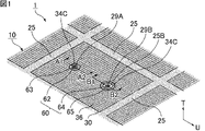
- FIG. 1 is a schematic perspective view showing a capacitor array in which examples of the capacitors of the present invention are arranged in an array.
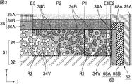
- FIG. 2 is a schematic cross-sectional view showing an example of a cross section of the capacitor array including a cross section along line A1-A2 in FIG.
- FIG. 3 is a schematic cross-sectional view showing a state in which a region Z in FIG. 2 is enlarged.
- FIG. 4 is a schematic cross-sectional view showing an example of a cross section of the capacitor array including a cross section along line B1-B2 in FIG.
- the capacitor of the present invention will be described below. It should be noted that the present invention is not limited to the following configurations, and may be modified as appropriate without departing from the gist of the present invention.
- the present invention also includes a combination of a plurality of individual preferred configurations described below.
- a capacitor of the present invention includes a capacitor layer having a capacitor portion, and a through-hole conductor provided to penetrate the capacitor portion in the thickness direction of the capacitor layer.
- FIG. 1 is a schematic perspective view showing a capacitor array in which an example of the capacitors of the present invention are arranged in an array.
- the capacitor array 1 shown in FIG. 1 has capacitor layers 10 and through-hole conductors 60 .
- the capacitor layer 10 may have a plurality of capacitor sections 30 as shown in FIG. 1 or may have one capacitor section 30 .
- the capacitor layer 10 has a plurality of capacitor portions 30, it is preferable that the plurality of capacitor portions 30 be divided by a plurality of penetrating portions and arranged in a plane. Note that each of the plurality of capacitor units 30 constitutes a capacitor.
- the plurality of capacitor portions 30 may be arranged linearly or in a plane. Moreover, the plurality of capacitor portions 30 may be arranged regularly or may be arranged irregularly. The size, planar shape, etc. of the plurality of capacitor portions 30 may all be the same, or part or all of them may be different.
- the capacitor layer 10 may include two or more types of capacitor portions 30 having different areas.
- the capacitor layer 10 may include a capacitor portion 30 whose planar shape is not rectangular.
- rectangle means square or rectangle. Therefore, the capacitor layer 10 includes capacitor portions 30 having planar shapes other than rectangles, polygons such as triangles, pentagons, and hexagons, shapes including curved portions, circles, ovals, and the like. good too.
- the capacitor layer 10 may include two or more types of capacitor portions 30 having different planar shapes.
- the capacitor layer 10 may or may not include the capacitor portion 30 having a rectangular planar shape in addition to the capacitor portion 30 having a non-rectangular planar shape.
- the capacitor array 1 corresponds to a single capacitor.
- the through-hole conductors 60 are each provided to pass through the capacitor section 30 in the thickness direction T of the capacitor layer 10 .
- the capacitor portion includes an anode plate having a porous layer on at least one main surface, a dielectric layer provided on the surface of the porous layer, and a dielectric layer provided on the surface of the dielectric layer. a cathode layer;
- FIG. 2 is a schematic cross-sectional view showing an example of a cross section of the capacitor array including a cross section along line A1-A2 in FIG.
- the line segment A1-A2 in FIG. 2 corresponds to the line segment A1-A2 in FIG.
- the capacitor section 30 has an anode plate 31, a dielectric layer 35, and a cathode layer .
- the anode plate 31 has a core portion 32 and a porous layer 34 .
- the core part 32 is preferably made of metal, and more preferably made of valve action metal.
- valve action metals include single metals such as aluminum, tantalum, niobium, titanium, and zirconium, and alloys containing at least one of these single metals. Among them, aluminum or an aluminum alloy is preferable.
- the porous layer 34 is provided on at least one main surface of the core portion 32 . That is, the porous layer 34 may be provided only on one main surface of the core portion 32, or may be provided on both main surfaces of the core portion 32 as shown in FIG. Thus, anode plate 31 has porous layer 34 on at least one main surface.
- the porous layer 34 is preferably an etching layer obtained by etching the surface of the anode plate 31 .
- the shape of the anode plate 31 is preferably flat plate-like, more preferably foil-like.
- plate-like also includes “foil-like”.
- the dielectric layer 35 is provided on the surface of the porous layer 34 . More specifically, the dielectric layer 35 is provided along the surface (contour) of each hole present in the porous layer 34 .
- the dielectric layer 35 is preferably made of an oxide film of the valve action metal described above.
- the anode plate 31 is an aluminum foil
- the anode plate 31 is anodized (also called a chemical conversion treatment) in an aqueous solution containing ammonium adipate or the like to form an oxide film that becomes the dielectric layer 35. is formed. Since the dielectric layer 35 is formed along the surface of the porous layer 34, the dielectric layer 35 is provided with pores (recesses).
- the cathode layer 36 is provided on the surface of the dielectric layer 35 .
- the cathode layer 36 may have a solid electrolyte layer 36A provided on the surface of the dielectric layer 35 and a conductor layer 36B provided on the surface of the solid electrolyte layer 36A. preferable.
- constituent materials of the solid electrolyte layer 36A include conductive polymers such as polypyrroles, polythiophenes, and polyanilines. Among them, polythiophenes are preferred, and poly(3,4-ethylenedioxythiophene) (PEDOT) is particularly preferred. Also, the conductive polymer may contain a dopant such as polystyrene sulfonic acid (PSS).
- conductive polymers such as polypyrroles, polythiophenes, and polyanilines.
- PEDOT poly(3,4-ethylenedioxythiophene)
- PES polystyrene sulfonic acid
- the solid electrolyte layer 36A preferably includes an inner layer that fills the pores (recesses) of the dielectric layer 35 and an outer layer that covers the surface of the dielectric layer 35.
- the conductor layer 36B preferably includes at least one of a conductive resin layer and a metal layer. That is, the conductor layer 36B may contain only the conductive resin layer, may contain only the metal layer, or may contain both the conductive resin layer and the metal layer.
- the conductive resin layer examples include a conductive adhesive layer containing at least one conductive filler selected from the group consisting of silver filler, copper filler, nickel filler, and carbon filler.
- metal layers include metal plating films and metal foils.
- the metal layer is preferably made of at least one metal selected from the group consisting of nickel, copper, silver, and an alloy containing at least one of these metals as a main component.
- the main component means the element component with the highest weight ratio.
- the conductor layer 36B may include, for example, a carbon layer provided on the surface of the solid electrolyte layer 36A and a copper layer provided on the surface of the carbon layer.
- the carbon layer is formed in a predetermined region by applying carbon paste to the surface of the solid electrolyte layer 36A by, for example, a sponge transfer method, screen printing method, dispenser coating method, inkjet printing method, or the like.
- the copper layer is formed in a predetermined region by applying copper paste to the surface of the carbon layer by, for example, a sponge transfer method, screen printing method, spray coating method, dispenser coating method, inkjet printing method, or the like.
- the capacitor section 30 shown in FIG. and a cathode layer 36 provided on the surface of layer 35 .
- the capacitor part 30 constitutes an electrolytic capacitor.
- the cathode layer 36 has the solid electrolyte layer 36A
- the capacitor section 30 constitutes a solid electrolytic capacitor.
- the through-hole conductor includes a first through-hole conductor provided on at least the inner wall surface of the first through-hole penetrating the capacitor portion in the thickness direction, and the first through-hole conductor extends in the thickness direction. It is electrically connected to the end surface of the anode plate that faces the inner wall surface of the first through hole in the orthogonal plane direction.
- the first through-hole conductors 62 are provided so as to penetrate the capacitor section 30 in the thickness direction T of the capacitor layer 10 . More specifically, the first through-hole conductor 62 is provided on at least the inner wall surface of the first through-hole 63 that penetrates the capacitor section 30 in the thickness direction T. As shown in FIG. 2, the first through-hole conductors 62 are provided so as to penetrate the capacitor section 30 in the thickness direction T of the capacitor layer 10 . More specifically, the first through-hole conductor 62 is provided on at least the inner wall surface of the first through-hole 63 that penetrates the capacitor section 30 in the thickness direction T. As shown in FIG.
- the first through-hole conductor 62 is electrically connected to the end surface of the anode plate 31 facing the inner wall surface of the first through-hole 63 in the plane direction U orthogonal to the thickness direction T. In the example shown in FIG. 2 , the first through-hole conductor 62 is connected to the end surface of the anode plate 31 .
- the core portion 32 and the porous layer 34 are exposed on the end face of the anode plate 31 electrically connected to the first through-hole conductor 62 . Therefore, the porous layer 34 as well as the core 32 are electrically connected to the first through-hole conductors 62 .
- the first through-hole conductors 62 are formed, for example, as follows. First, a first through hole 63 is formed by drilling, laser processing, or the like on a portion where the first through hole conductor 62 is to be formed. Then, the first through-hole conductor 62 is formed by metallizing the inner wall surface of the first through-hole 63 with a low-resistance metal such as copper, gold, or silver. When forming the first through-hole conductor 62, for example, metallizing the inner wall surface of the first through-hole 63 by electroless copper plating, electrolytic copper plating, or the like facilitates processing.
- the method of forming the first through-hole conductor 62 in addition to the method of metallizing the inner wall surface of the first through-hole 63, the method of filling the first through-hole 63 with a metal, a composite material of metal and resin, or the like. may be
- the first through-hole conductor preferably has an anode connection layer located on the end surface side of the anode plate, and the anode connection layer is preferably in contact with the end surface of the anode plate.
- the first through-hole conductor 62 preferably has an anode connection layer 68 located on the end surface side of the anode plate 31. As shown in FIG. Moreover, as shown in FIG. 2, the anode connection layer 68 is preferably in contact with the end surface of the anode plate 31 .
- the anode connection layer 68 serves as a barrier layer for the anode plate 31 , more specifically, the core portion 32 . and a barrier layer against the porous layer 34 .
- the anode connection layer 68 may include a first anode connection layer 68A and a second anode connection layer 68B in order from the end face side of the anode plate 31.
- the first anode connection layer 68A may be a layer containing zinc as a main component
- the second anode connection layer 68B may be a layer containing nickel or copper as a main component.
- the first anode connection layer 68A is formed on the end surface of the anode plate 31 by, for example, zincate displacement deposition, and then the second anode connection layer 68B is formed by, for example, electroless nickel plating.
- it is formed on the surface of the first anode connection layer 68A by electroless copper plating.
- the first anode connection layer 68A may disappear when the second anode connection layer 68B is formed.
- the anode connection layer 68 may consist of only the second anode connection layer 68B.
- the anode connection layer 68 preferably contains a layer containing nickel as a main component. In this case, damage to the metal (for example, aluminum) constituting the anode plate 31 is reduced, so the barrier properties of the anode connection layer 68 against the anode plate 31 are likely to be improved.
- the dimensions of the anode connection layer 68 in the thickness direction T are preferably larger than the dimensions of the anode plate 31 .
- the barrier properties of the anode connection layer 68 against the anode plate 31 are likely to be improved.
- the dimension of the anode connection layer 68 in the thickness direction T is preferably greater than 100% and less than or equal to 200% of the dimension of the anode plate 31 .
- the dimensions of the anode connection layer 68 in the thickness direction T may be the same as the dimensions of the anode plate 31 or may be smaller than the dimensions of the anode plate 31 .
- first through-hole conductor 62 may not have the anode connection layer 68 located on the end surface side of the anode plate 31 .
- the first through-hole conductor is electrically connected to the end face of the anode plate over the entire circumference of the first through-hole when viewed from the thickness direction.
- the first through-hole conductor 62 when viewed in the thickness direction T, is electrically connected to the end surface of the anode plate 31 over the entire circumference of the first through-hole 63.
- the first through-hole conductor 62 has the anode connection layer 68 located on the end surface side of the anode plate 31, when viewed from the thickness direction T, the anode in the first through-hole conductor 62 Portions other than the connection layer 68 are preferably connected to the anode connection layer 68 over the entire circumference of the first through hole 63 .
- the connection resistance between the anode connection layer 68 and the portion other than the anode connection layer 68 in the first through-hole conductor 62 decreases. easier to do.
- the connection resistance between the first through-hole conductor 62 and the anode plate 31 is easily reduced, so that the equivalent series resistance (ESR) of the capacitor section 30 is easily reduced.
- ESR equivalent series resistance
- the capacitor array 1 may further have conductive portions 20 electrically connected to the first through-hole conductors 62 .
- the conductive portion 20 is provided on the surface of the first through-hole conductor 62 .
- the conductive portion 20 can function as a connection terminal of the capacitor array 1 , more specifically, the capacitor portion 30 .
- the constituent material of the conductive portion 20 examples include low-resistance metals such as silver, gold, and copper.
- the conductive portion 20 is formed by plating the surface of the first through-hole conductor 62, for example.
- Silver filler A mixed material of resin and at least one conductive filler selected from the group consisting of copper filler, nickel filler, and carbon filler may be used.
- the capacitor array 1, more specifically, the capacitors constituting the capacitor array 1 further include a first resin-filled portion 29A formed by filling the first through holes 63 with a resin material. It is preferable to have In the example shown in FIGS. 1 and 2, the first resin-filled portion 29A is provided in a space surrounded by the first through-hole conductors 62 on the inner wall surface of the first through-hole 63 . When the space in the first through-hole 63 is eliminated by providing the first resin-filled portion 29A, the occurrence of delamination of the first through-hole conductor 62 is suppressed.
- the coefficient of thermal expansion of the first resin-filled portion 29A is preferably larger than that of the first through-hole conductor 62. More specifically, the coefficient of thermal expansion of the resin material filled in the first through-holes 63 is preferably higher than the coefficient of thermal expansion of the constituent material (for example, copper) of the first through-hole conductors 62 .
- the first resin filling portion 29A more specifically, the resin material filled in the first through-hole 63 expands in a high-temperature environment, causing the first through-hole conductor 62 to move in the first through-hole 63. Since it is pressed against the inner wall surface of the first through-hole 63 from the inside toward the outside, the occurrence of delamination of the first through-hole conductor 62 is sufficiently suppressed.
- the coefficient of thermal expansion of the first resin-filled portion 29A may be the same as the coefficient of thermal expansion of the first through-hole conductor 62, or may be smaller than the coefficient of thermal expansion of the first through-hole conductor 62. More specifically, the coefficient of thermal expansion of the resin material filled in the first through-holes 63 may be the same as the coefficient of thermal expansion of the constituent material of the first through-hole conductors 62, or the first through-hole conductors It may be less than the coefficient of thermal expansion of the constituent material of 62 .
- the capacitor array 1, more specifically, the capacitors forming the capacitor array 1 may not have the first resin filling portion 29A.
- the first through-hole conductors 62 are preferably provided not only on the inner wall surface of the first through-hole 63 but also in the entire interior of the first through-hole 63 .
- the capacitor layer 10 preferably further has an insulating portion 25 provided on the surface of the capacitor portion 30 .
- the insulating portion 25 includes a first insulating portion 25A provided on the surface of the capacitor portion 30 and a second insulating portion 25B provided on the surface of the first insulating portion 25A. is preferred.
- the constituent materials of the first insulating portion 25A and the second insulating portion 25B include, for example, resin materials such as epoxy, phenol, and polyimide, or resin materials such as epoxy, phenol, and polyimide, and inorganic fillers such as silica and alumina. and the like.
- the constituent material of the first insulating portion 25A and the constituent material of the second insulating portion 25B may be the same as or different from each other.
- the porous layer has the first holes, and the insides of the first holes contain part of the first through-hole conductors.
- FIG. 3 is a cross-sectional schematic diagram showing a state in which the region Z in FIG. 2 is enlarged.
- the dielectric layer 35 is provided on the surface of the porous layer 34, more specifically, along the surface (contour) of each hole present in the porous layer 34. ing.
- the porous layer 34 has first holes 34A.
- a part of the first through-hole conductor 62 is included inside the first hole 34A.
- the interior of the first hole 34A includes a portion of the anode connection layer 68, more specifically, a portion of the first anode connection layer 68A.
- problems such as peeling between the porous layer 34 and the first through-hole conductor 62, more specifically, peeling between the porous layer 34 and the anode connection layer 68 are less likely to occur.
- the reliability of the array 1 is improved, and in turn the reliability of the capacitors forming the capacitor array 1 is improved.
- the presence of the first hole in which part of the first through-hole conductor is contained in the porous layer is confirmed, for example, as follows. First, by cutting the capacitor, here, the capacitor array, the porous layer and the first through-hole conductor pass through the center of the first through-hole when viewed from the thickness direction as shown in FIG. A cross-section of the capacitor along the included thickness direction is exposed. Next, a scanning electron microscope (SEM) is used to take an enlarged image of the porous layer as shown in FIG. 3 in the exposed cross section of the capacitor, here the exposed cross section of the capacitor array.
- SEM scanning electron microscope
- element mapping is performed on the obtained enlarged image by wavelength dispersive X-ray spectroscopy (WDX), energy dispersive X-ray spectroscopy (EDX), or the like, so that the first through in the porous layer A first hole in which part of the hole conductor is included is confirmed.
- WDX wavelength dispersive X-ray spectroscopy
- EDX energy dispersive X-ray spectroscopy
- the first holes are present on the end surface of the porous layer forming the end surface of the anode plate.
- the first holes 34A are preferably present on the end surface of the porous layer 34 forming the end surface of the anode plate 31 .
- the porous layer 34 may be in a state before part of the first through-hole conductor 62 is included in the inside of the first hole 34A. It can be said that the end face of the film has fine irregularities.
- the first through-hole conductors 62 connected to the end face of the porous layer 34 are arranged in the concave portions of the end face of the porous layer 34, more specifically, It enters the first hole 34A.
- the first through-hole conductor 62 has an anode connection layer 68 positioned on the end surface side of the anode plate 31, the end surface of the porous layer 34 is finely uneven.
- the anode connection layer 68 more specifically the first anode connection layer 68A, enters the recess of the end face of the porous layer 34, more specifically the first hole 34A.
- the adhesion between the porous layer 34 and the anode connection layer 68 is more easily improved.
- problems such as peeling between the porous layer 34 and the anode connection layer 68 are less likely to occur, so the reliability of the capacitor array 1 is further improved, and the reliability of the capacitors constituting the capacitor array 1 is improved. is better.
- the porous layer further has a second hole, the second hole contains an insulating material, and the porous layer has the insulating material inside the second hole.
- the outer end of the insulating region on the first through-hole conductor side is located on the opposite side of the first through-hole conductor from the outer end of the porous layer on the first through-hole conductor side in the plane direction. preferably located.
- the porous layer 34 further has second holes 34B.
- the porous layer 34 includes an insulating region where the insulating material 34C inside the second holes 34B is present. Since the porous layer 34 includes an insulating region, the insulation between the anode plate 31 and the cathode layer 36 is ensured, and a short circuit between them is prevented.
- the hatched area of the insulating material 34C corresponds to the insulating area.
- the insulating region is not a continuous region within the porous layer 34 but a discontinuous region.
- the insulating region where the insulating material 34C is present is preferably provided around the first through-hole conductor 62. As shown in FIG. In this case, sufficient insulation is ensured between the anode plate 31 and the cathode layer 36, and short circuits between the two are sufficiently prevented.
- Examples of the insulating material 34C include resin materials such as epoxy, phenol, and polyimide, or mixed materials of resin materials such as epoxy, phenol, and polyimide, and inorganic fillers such as silica and alumina.
- the outer end E1 of the insulating region on the side of the first through-hole conductor 62 is located further than the outer end E2 of the porous layer 34 on the side of the first through-hole conductor 62. It is located on the opposite side (here, left side) of the hole conductor 62 .
- the surface area of the end face of the porous layer 34 forming the end face of the anode plate 31, which is made of a material (for example, aluminum) other than the insulating material 34C, is increased.
- the coverage of the first through-hole conductor 62 connected to the end face of the porous layer 34 improves.
- the end surface of the porous layer 34 may be made of a material other than the insulating material 34C.
- the improved coverage of the anode connection layer 68 with respect to the end surface of the porous layer 34 improves the barrier properties of the anode connection layer 68 with respect to the porous layer 34 , which in turn improves the barrier properties of the anode connection layer 68 with respect to the anode plate 31 . .
- the dissolution of the anode plate 31 that occurs during the chemical treatment for forming the conductive portion 20 and the like is suppressed, and thus the intrusion of the chemical into the capacitor portion 30 is suppressed. Therefore, the reliability of the capacitor array 1 is further improved, and the reliability of the capacitors forming the capacitor array 1 is further improved.
- the porous layer 34 As a result, the equivalent series resistance of the capacitor section 30 is reduced, so that the reliability of the capacitor array 1 is further improved, and the reliability of the capacitors forming the capacitor array 1 is further improved.
- the outer end of the insulating region on the side of the first through-hole conductor passes through the center of the first through-hole when viewed in the thickness direction as shown in FIG. 2 and includes the porous layer and the first through-hole conductor.
- a capacitor here a capacitor array
- a scanning electron microscope is used to take an enlarged image of the porous layer as shown in FIG. 3 in the exposed cross section of the capacitor, here the exposed cross section of the capacitor array.
- the insulating region where the insulating material exists is confirmed in the porous layer. Then, in the planar direction, the end of the insulating region closest to the first through-hole conductor is defined as the outer end of the insulating region on the first through-hole conductor side.
- the outer end of the porous layer on the side of the first through-hole conductor is determined, for example, as follows. First, the entire range of the porous layer including the insulating region is confirmed by performing elemental mapping on the enlarged image obtained by the above-described method by wavelength dispersive X-ray spectroscopy. Then, in the plane direction, the end of the porous layer closest to the first through-hole conductor is defined as the outer end of the porous layer on the first through-hole conductor side.
- the outer end of the insulating region on the side of the first through-hole conductor defined by the method described above is the outer end of the porous layer on the side of the first through-hole conductor defined by the method described above. It may be located on the side opposite to the first through-hole conductor from the end.
- the insulating material is filled into the pores inside the porous layer, and then plasma treatment or the like is applied to the vicinity of the end face of the porous layer.
- plasma treatment or the like is applied to the vicinity of the end face of the porous layer.
- the distance between the outer end E1 of the insulating region on the first through-hole conductor 62 side and the outer end E2 of the porous layer 34 on the first through-hole conductor 62 side is preferably greater than 0 ⁇ m. , less than 20 ⁇ m.
- the area ratio of voids is preferably 0 area % or more and 30 area % or less.
- a first region R1 extending from an outer end E2 on the side of the first through-hole conductor 62 to a position P1 separated by the thickness of the porous layer 34 in the plane direction U is formed.
- the area ratio of voids in the first region R1 is preferably 0 area % or more and 30 area % or less. That is, in the first region R1 in the vicinity of the end face of the porous layer 34, the area ratio of voids in which all materials including the first through-hole conductor 62 and the insulating material 34C are not contained is 0 area% or more and 30 area%. % or less.
- the porous layer 34 is formed through the gaps. Excessive etching of the vicinity of the end face of 34 is suppressed. As a result, corrosion due to chlorine, water, etc. remaining inside the porous layer 34 is suppressed, so that the reliability of the capacitor array 1 is further improved, and the reliability of the capacitors constituting the capacitor array 1 is further improved. do.
- the first through-hole conductor 62 connected to the end surface of the porous layer 34 is subjected to zincate treatment.
- the porous layer 34 is formed by the first plating process, the vicinity of the end surface of the porous layer 34 is excessively etched through the voids, resulting in a larger space inside the porous layer 34 .
- corrosion occurs due to chlorine, water, etc. remaining inside the porous layer 34, which lowers the reliability of the capacitor array 1, which in turn lowers the reliability of the capacitors forming the capacitor array 1.
- the area ratio of the voids in the first region is, as shown in FIG.
- a capacitor here a capacitor array
- a scanning electron microscope is used to take an enlarged image of the porous layer as shown in FIG. 3 in the exposed cross section of the capacitor, here the exposed cross section of the capacitor array.
- elemental mapping on the obtained enlarged image by wavelength dispersive X-ray spectroscopy, the regions where voids exist are confirmed in the porous layer.
- the gaps exposed at the end face of the porous layer are also included in the above-described void existence region.
- the outer end of the porous layer on the side of the first through-hole conductor is determined by the method described above, and the porous layer extends from the outer end on the side of the first through-hole conductor in the plane direction by the thickness of the porous layer. Identify a first region that spans to a remote location. Then, the area ratio of the void existing region in the first region is measured by image analysis software. Then, the measured area ratio is determined as the area ratio of voids in the first region.
- the regions where voids exist are confirmed by performing elemental mapping on the exposed cross section of the capacitor by combining scanning electron microscopy and wavelength dispersive X-ray spectroscopy.
- the region where voids exist may be confirmed by another analysis method such as elemental mapping that combines electron microscopy and energy dispersive X-ray spectroscopy.
- voids 34V that do not contain any material including first through-hole conductors 62 and insulating material 34C, are shown as voids. , the second hole 34B, etc., which are inside the holes containing some material and which are not completely filled with the material.
- the insulating material is filled into the pores inside the porous layer, and then plasma treatment or the like is applied to the vicinity of the end face of the porous layer.
- the area ratio of the voids in the first region is preferably adjusted to 0 area % or more and 30 area % or less.
- the range from the outer end of the insulating region on the side opposite to the first through-hole conductor to the position away from the first through-hole conductor in the plane direction by the thickness of the porous layer When the second region is determined to span the region, the area ratio of voids in the second region is preferably larger than the area ratio of voids in the first region.
- the thickness of the porous layer 34 extends toward the first through-hole conductor 62 in the planar direction U.
- the area ratio of the voids in the second region R2 is preferably larger than the area ratio of the voids in the first region R1.
- the area ratio of the voids in the second region R2 is higher than the area ratio of the voids in the first region R1. growing.
- the range of the insulating region in the second region R2 is smaller than the range of the insulating region in the first region R1.
- the insulating material 34C when filling the second holes 34B with the insulating material 34C, for example, by providing the insulating material 34C on the surface of the porous layer 34 (dielectric layer 35), the insulating material 34C is applied to the surface of the porous layer 34. It permeates from the surface along the thickness direction T, more specifically, from the surface of the porous layer 34 toward the core portion 32 .
- the portion located on the opposite side of the first through-hole conductor 62 is located on the surface of the porous layer 34, the first through-hole conductor It expands in the surface direction U toward the opposite side of 62 .
- the portion located on the opposite side of the first through-hole conductor 62 penetrates in the thickness direction T inside the porous layer 34. , seeps out in the surface direction U toward the side opposite to the first through-hole conductor 62 .
- the insulating material 34 ⁇ /b>C oozes out in the surface direction U in this manner, the oozing width becomes smaller from the surface of the porous layer 34 toward the core portion 32 .
- a leaking region of the insulating material 34C is formed as a region in the vicinity of the outer end E3 on the opposite side of the first through-hole conductor 62 in the insulating region in the porous layer 34 .
- the insulating region that exists in the second region R2 includes the bleeding region of the insulating material 34C. Therefore, the range of the insulating region in the second region R2 is smaller than the range of the insulating region in the first region R1. That is, the area ratio of voids in the second region R2 is larger than the area ratio of voids in the first region R1.
- the insulating material 34C formed by the above-described method seeps into the second region R2. It can be said that the area exists.
- the area ratio of the voids in the second region is, as shown in FIG.
- the porous layer and, in the porous layer, a second region extending from the outer end of the insulating region opposite to the first through-hole conductor to a position spaced apart by the thickness of the porous layer in the planar direction toward the first through-hole conductor. to confirm.
- the area ratio of the void existing region in the second region is measured by image analysis software. Then, the measured area ratio is determined as the area ratio of voids in the second region.
- the area ratio of voids in the first region R1 is preferably larger than 0% and smaller than 80% with respect to the area ratio of voids in the second region R2.
- the porous layer 34 includes, in addition to the first holes 34A, the second holes 34B, and the holes 34V, materials other than the first through-hole conductors 62 and the insulating material 34C, such as , there may be holes in which the solid electrolyte layer 36A is contained.
- the through-hole conductor further includes a second through-hole conductor provided on at least the inner wall surface of the second through-hole penetrating in the thickness direction of the capacitor portion provided with the first through-hole conductor, Preferably, the second through-hole conductor is electrically connected to the cathode layer.
- FIG. 4 is a schematic cross-sectional view showing an example of a cross-section of the capacitor array including a cross-section taken along line segment B1-B2 in FIG.
- the line segment B1-B2 in FIG. 4 corresponds to the line segment B1-B2 in FIG.
- the capacitor array 1 more specifically, the capacitors forming the capacitor array 1 preferably further have a second through-hole conductor 64 .
- the second through-hole conductor 64 is provided so as to penetrate the capacitor section 30 in the thickness direction T of the capacitor layer 10 . More specifically, the second through-hole conductor 64 is formed on at least the inner wall surface of the second through-hole 65 penetrating in the thickness direction T through the capacitor section 30 provided with the first through-hole conductor 62 shown in FIG. is preferably provided.
- the second through-hole conductors 64 are preferably electrically connected to the cathode layer 36, as shown in FIG.
- the conductive portion 40 is provided on the surface of the second through-hole conductor 64 and can function as a connection terminal of the capacitor array 1 , more specifically, the capacitor portion 30 .
- via conductors 42 are provided so as to pass through insulating portion 25 in thickness direction T and be connected to conductive portion 40 and cathode layer 36 . Therefore, in the example shown in FIG. 4, the second through-hole conductor 64 is electrically connected to the cathode layer 36 through the conductive portion 40 and the via conductor 42 . In this case, the size of the capacitor array 1 can be reduced, and thus the size of the capacitors forming the capacitor array 1 can be reduced.
- the second through-hole conductors 64 are formed, for example, as follows. First, a through-hole is formed by drilling, laser processing, or the like in a portion where the second through-hole conductor 64 is to be formed. Next, an insulating layer is formed by filling the formed through-hole with a constituent material (for example, a resin material) of the second insulating portion 25B. Then, the formed insulating layer is subjected to drilling, laser processing, or the like to form the second through hole 65 . At this time, by making the diameter of the second through-hole 65 smaller than the diameter of the insulating layer, the constituent material of the second insulating portion 25B exists between the previously formed through-hole 65 and the second through-hole 65.
- a through-hole is formed by drilling, laser processing, or the like in a portion where the second through-hole conductor 64 is to be formed.
- an insulating layer is formed by filling the formed through-hole with a constituent material (for example, a resin material) of the second insulating
- the inner wall surface of the second through-hole 65 is metallized with a low-resistance metal such as copper, gold, or silver to form the second through-hole conductor 64 .
- a low-resistance metal such as copper, gold, or silver
- metallizing the inner wall surface of the second through-hole 65 by electroless copper plating, electrolytic copper plating, or the like facilitates processing.
- the method of forming the second through-hole conductor 64 in addition to the method of metallizing the inner wall surface of the second through-hole 65, the method of filling the second through-hole 65 with a metal, a composite material of metal and resin, or the like. may be
- the constituent material of the conductive portion 40 examples include low-resistance metals such as silver, gold, and copper.
- the conductive portion 40 is formed by, for example, plating the surface of the second through-hole conductor 64 .
- Silver filler A mixed material of resin and at least one conductive filler selected from the group consisting of copper filler, nickel filler, and carbon filler may be used.
- the constituent material of the via conductor 42 for example, the same constituent material as that of the conductive portion 40 can be used.
- the inner wall surface of the through-hole provided to penetrate the insulating portion 25 in the thickness direction T is subjected to a plating process, or a heat treatment is performed after filling the conductive paste. formed by
- the capacitor array 1, more specifically, the capacitors constituting the capacitor array 1 further include a second resin-filled portion 29B in which the second through-hole 65 is filled with a resin material. It is preferable to have In the example shown in FIGS. 1 and 4, the second resin filling portion 29B is provided in a space surrounded by the second through-hole conductors 64 on the inner wall surface of the second through-hole 65. As shown in FIG. When the space in the second through-hole 65 is eliminated by providing the second resin-filled portion 29B, the occurrence of delamination of the second through-hole conductor 64 is suppressed.
- the coefficient of thermal expansion of the second resin-filled portion 29B is preferably larger than that of the second through-hole conductors 64 . More specifically, the coefficient of thermal expansion of the resin material filling the second through-holes 65 is preferably higher than the coefficient of thermal expansion of the constituent material (for example, copper) of the second through-hole conductors 64 .
- the second through-hole conductors 64 are pushed out of the second through-holes 65 by expanding the second resin-filled portion 29B, more specifically, the resin material filled in the second through-holes 65 in a high-temperature environment. Since it is pressed against the inner wall surface of the second through-hole 65 from the inside toward the outside, the occurrence of delamination of the second through-hole conductor 64 is sufficiently suppressed.
- the coefficient of thermal expansion of the second resin-filled portion 29B may be the same as the coefficient of thermal expansion of the second through-hole conductor 64, or may be smaller than the coefficient of thermal expansion of the second through-hole conductor 64. More specifically, the coefficient of thermal expansion of the resin material filled in the second through-holes 65 may be the same as the coefficient of thermal expansion of the constituent material of the second through-hole conductors 64. It may be less than the coefficient of thermal expansion of the constituent material of 64.
- the capacitor array 1, more specifically, the capacitors forming the capacitor array 1 may not have the second resin filling portion 29B.
- the second through-hole conductors 64 are preferably provided not only on the inner wall surface of the second through-hole 65 but also in the entire interior of the second through-hole 65 .
- the capacitor layer further has a first insulating portion provided on the surface of the capacitor portion, and a second insulating portion provided on the surface of the first insulating portion.
- the section extends between the anode plate and the second through-hole conductor.
- the capacitor layer 10 further has an insulating portion 25 provided on the surface of the capacitor portion 30 .
- the insulating portion 25 includes a first insulating portion 25A provided on the surface of the capacitor portion 30 and a second insulating portion 25A provided on the surface of the first insulating portion 25A. It is preferable to include a portion 25B and a.
- the capacitor layer 10 further has a first insulating portion 25A provided on the surface of the capacitor portion 30 and a second insulating portion 25B provided on the surface of the first insulating portion 25A. is preferred.
- the second insulating portion 25B extends between the anode plate 31 and the second through-hole conductor 64 as shown in FIG. preferably.
- the second insulating portion 25B contacts both the anode plate 31 and the second through-hole conductor 64 . Since the second insulating portion 25B extends between the anode plate 31 and the second through-hole conductor 64, the insulation between the anode plate 31 and the second through-hole conductor 64 and the anode plate 31 and the cathode layer 36 to prevent a short circuit therebetween.
- the portion 32 and the porous layer 34 are exposed.
- problems such as peeling between the second insulating portion 25B and the porous layer 34 occur. becomes less likely to occur.
- an insulating region is provided around the second through-hole conductor 64 in which insulating material 34C resides, as shown.
- the insulation between the anode plate 31 and the second through-hole conductor 64, and the insulation between the anode plate 31 and the cathode layer 36, is sufficiently ensured, and a short circuit between the two is sufficiently prevented. be.
- the constituent material of the second insulating portion 25B enters the pores of the porous layer 34.
- the mechanical strength of the porous layer 34 is improved, the occurrence of delamination caused by the pores of the porous layer 34 is suppressed.
- the coefficient of thermal expansion of the second insulating portion 25B is preferably larger than the coefficient of thermal expansion of the second through-hole conductor 64 . More specifically, the coefficient of thermal expansion of the constituent material of the second insulating portion 25B is preferably higher than the coefficient of thermal expansion of the constituent material (for example, copper) of the second through-hole conductors 64 . In this case, the porous layer 34 and the second through-hole conductor 64 are pressed down by expansion of the second insulating portion 25B, more specifically, the constituent material of the second insulating portion 25B in a high-temperature environment. The occurrence of lamination is sufficiently suppressed.
- the coefficient of thermal expansion of the second insulating portion 25B may be the same as the coefficient of thermal expansion of the second through-hole conductor 64, or may be smaller than the coefficient of thermal expansion of the second through-hole conductor 64. More specifically, the coefficient of thermal expansion of the material forming the second insulating portion 25B may be the same as the coefficient of thermal expansion of the material forming the second through-hole conductor 64. It may be smaller than the coefficient of thermal expansion of the material.
- the capacitor of the present invention is used, for example, in composite electronic components.
- a composite electronic component includes, for example, the capacitor of the present invention, an external electrode provided outside the capacitor of the present invention and electrically connected to each of the anode plate and the cathode layer, and and electronic components physically connected to each other.
- the electronic component electrically connected to the external electrode may be a passive element, an active element, or both a passive element and an active element, It may be a composite of passive and active elements.
- Passive elements include, for example, inductors.
- active elements include memory, GPU (Graphical Processing Unit), CPU (Central Processing Unit), MPU (Micro Processing Unit), PMIC (Power Management IC), and the like.
- the capacitor of the present invention When the capacitor of the present invention is used in a composite electronic component, the capacitor of the present invention is treated as a board for mounting the electronic component, for example, as described above. Therefore, by forming the capacitor of the present invention into a sheet as a whole and further by forming the electronic component mounted on the capacitor of the present invention into a sheet, the capacitor of the present invention can be formed via a through-hole conductor passing through the electronic component in the thickness direction. It becomes possible to electrically connect the capacitor and the electronic component in the thickness direction. As a result, it becomes possible to configure passive elements and active elements as electronic parts as a collective module.
- a switching regulator can be formed by electrically connecting the capacitor of the present invention between a voltage regulator including a semiconductor active element and a load to which the converted DC voltage is supplied.
- a circuit layer is formed on one main surface of a capacitor matrix sheet in which a plurality of capacitors of the present invention are laid out, and then the circuit layer is electrically connected to a passive element or an active element as an electronic component. can be connected directly.
- the capacitor of the present invention may be placed in a cavity provided in advance on a substrate, embedded with resin, and then the circuit layer may be formed on the resin.
- a passive element or an active element as another electronic component may be mounted in another cavity portion of the same substrate.
- the capacitor of the present invention is mounted on a smooth carrier such as a wafer or glass, and after forming an outer layer portion with resin, a circuit layer is formed, and the circuit layer is used as a passive element or an active element as an electronic component. may be electrically connected to
Landscapes
- Engineering & Computer Science (AREA)
- Power Engineering (AREA)
- Microelectronics & Electronic Packaging (AREA)
- Manufacturing & Machinery (AREA)
- Fixed Capacitors And Capacitor Manufacturing Machines (AREA)
Priority Applications (3)
| Application Number | Priority Date | Filing Date | Title |
|---|---|---|---|
| CN202280049856.0A CN117642833A (zh) | 2021-07-16 | 2022-06-02 | 电容器 |
| JP2023535175A JP7563605B2 (ja) | 2021-07-16 | 2022-06-02 | コンデンサ |
| US18/410,307 US12603233B2 (en) | 2021-07-16 | 2024-01-11 | Capacitor having a porous layer including a void containing at least part of a through-hole conductor |
Applications Claiming Priority (2)
| Application Number | Priority Date | Filing Date | Title |
|---|---|---|---|
| JP2021117803 | 2021-07-16 | ||
| JP2021-117803 | 2021-07-16 |
Related Child Applications (1)
| Application Number | Title | Priority Date | Filing Date |
|---|---|---|---|
| US18/410,307 Continuation US12603233B2 (en) | 2021-07-16 | 2024-01-11 | Capacitor having a porous layer including a void containing at least part of a through-hole conductor |
Publications (1)
| Publication Number | Publication Date |
|---|---|
| WO2023286484A1 true WO2023286484A1 (ja) | 2023-01-19 |
Family
ID=84919999
Family Applications (1)
| Application Number | Title | Priority Date | Filing Date |
|---|---|---|---|
| PCT/JP2022/022439 Ceased WO2023286484A1 (ja) | 2021-07-16 | 2022-06-02 | コンデンサ |
Country Status (5)
| Country | Link |
|---|---|
| US (1) | US12603233B2 (https=) |
| JP (1) | JP7563605B2 (https=) |
| CN (1) | CN117642833A (https=) |
| TW (1) | TWI831226B (https=) |
| WO (1) | WO2023286484A1 (https=) |
Families Citing this family (1)
| Publication number | Priority date | Publication date | Assignee | Title |
|---|---|---|---|---|
| TWI885959B (zh) * | 2023-07-28 | 2025-06-01 | 日商村田製作所股份有限公司 | 內建電容器之基板 |
Citations (4)
| Publication number | Priority date | Publication date | Assignee | Title |
|---|---|---|---|---|
| JP2007251101A (ja) * | 2006-03-20 | 2007-09-27 | Matsushita Electric Ind Co Ltd | 固体電解コンデンサ内蔵回路基板およびそれを用いたインターポーザおよびパッケージ |
| JP2008078301A (ja) * | 2006-09-20 | 2008-04-03 | Fujitsu Ltd | キャパシタ内蔵型配線基板およびその製造方法 |
| JP2008130722A (ja) * | 2006-11-20 | 2008-06-05 | Matsushita Electric Ind Co Ltd | 固体電解コンデンサ内蔵回路基板とその製造方法 |
| JP2012124281A (ja) * | 2010-12-07 | 2012-06-28 | Tdk Corp | 配線板、電子部品内蔵基板、配線板の製造方法及び電子部品内蔵基板の製造方法 |
Family Cites Families (11)
| Publication number | Priority date | Publication date | Assignee | Title |
|---|---|---|---|---|
| JPH08321666A (ja) | 1995-05-26 | 1996-12-03 | Matsushita Electric Works Ltd | プリント配線板、及び、その製造方法 |
| JP5011624B2 (ja) | 2001-08-30 | 2012-08-29 | 日本ケミコン株式会社 | 固体電解コンデンサ及びその製造方法 |
| JP4839824B2 (ja) * | 2005-12-21 | 2011-12-21 | パナソニック株式会社 | コンデンサ内蔵基板およびその製造方法 |
| JP4899775B2 (ja) * | 2006-10-13 | 2012-03-21 | パナソニック株式会社 | 固体電解コンデンサの製造方法と固体電解コンデンサ内蔵基板の製造方法 |
| KR100861619B1 (ko) | 2007-05-07 | 2008-10-07 | 삼성전기주식회사 | 방열 인쇄회로기판 및 그 제조방법 |
| TWI373118B (en) * | 2007-12-21 | 2012-09-21 | Ind Tech Res Inst | Through hole capacitor and method of manufacturing the same |
| JP2012128242A (ja) | 2010-12-16 | 2012-07-05 | Kaneka Corp | アクティブマトリクス型表示装置用基板 |
| TWI483352B (zh) * | 2012-03-12 | 2015-05-01 | Ind Tech Res Inst | 固態電解電容基板模組及包括該固態電解電容基板模組的電路板 |
| WO2019221046A1 (ja) * | 2018-05-16 | 2019-11-21 | 株式会社村田製作所 | 固体電解コンデンサ |
| JP2020053588A (ja) | 2018-09-27 | 2020-04-02 | 株式会社村田製作所 | 固体電解コンデンサ |
| JP7180561B2 (ja) * | 2019-03-29 | 2022-11-30 | 株式会社村田製作所 | コンデンサアレイ、及び、複合電子部品 |
-
2022
- 2022-05-30 TW TW111120022A patent/TWI831226B/zh active
- 2022-06-02 WO PCT/JP2022/022439 patent/WO2023286484A1/ja not_active Ceased
- 2022-06-02 CN CN202280049856.0A patent/CN117642833A/zh active Pending
- 2022-06-02 JP JP2023535175A patent/JP7563605B2/ja active Active
-
2024
- 2024-01-11 US US18/410,307 patent/US12603233B2/en active Active
Patent Citations (4)
| Publication number | Priority date | Publication date | Assignee | Title |
|---|---|---|---|---|
| JP2007251101A (ja) * | 2006-03-20 | 2007-09-27 | Matsushita Electric Ind Co Ltd | 固体電解コンデンサ内蔵回路基板およびそれを用いたインターポーザおよびパッケージ |
| JP2008078301A (ja) * | 2006-09-20 | 2008-04-03 | Fujitsu Ltd | キャパシタ内蔵型配線基板およびその製造方法 |
| JP2008130722A (ja) * | 2006-11-20 | 2008-06-05 | Matsushita Electric Ind Co Ltd | 固体電解コンデンサ内蔵回路基板とその製造方法 |
| JP2012124281A (ja) * | 2010-12-07 | 2012-06-28 | Tdk Corp | 配線板、電子部品内蔵基板、配線板の製造方法及び電子部品内蔵基板の製造方法 |
Also Published As
| Publication number | Publication date |
|---|---|
| US12603233B2 (en) | 2026-04-14 |
| CN117642833A (zh) | 2024-03-01 |
| US20240186071A1 (en) | 2024-06-06 |
| JPWO2023286484A1 (https=) | 2023-01-19 |
| JP7563605B2 (ja) | 2024-10-08 |
| TW202305846A (zh) | 2023-02-01 |
| TWI831226B (zh) | 2024-02-01 |
Similar Documents
| Publication | Publication Date | Title |
|---|---|---|
| CN116235264B (zh) | 电容器阵列 | |
| JP7732589B2 (ja) | コンデンサ | |
| US20250104933A1 (en) | Capacitor element | |
| WO2023238681A1 (ja) | コンデンサアレイ | |
| WO2023286484A1 (ja) | コンデンサ | |
| US20250166927A1 (en) | Capacitor element | |
| CN223785015U (zh) | 电容器元件 | |
| US20240332346A1 (en) | Module and semiconductor composite device | |
| JP7776019B2 (ja) | コンデンサ素子 | |
| CN119256382A (zh) | 固体电解电容器和电容器阵列 | |
| JP7729487B2 (ja) | コンデンサアレイ | |
| US20250087429A1 (en) | Capacitor array | |
| US20250357053A1 (en) | Capacitor element | |
| WO2025243714A1 (ja) | コンデンサ素子 | |
| WO2026048931A1 (ja) | コンデンサ素子 | |
| WO2024214424A1 (ja) | コンデンサ素子 | |
| WO2026048934A1 (ja) | コンデンサ素子 | |
| WO2026048925A1 (ja) | コンデンサ素子 | |
| TW202505953A (zh) | 內建電容器之基板 | |
| WO2024247589A1 (ja) | コンデンサ素子 |
Legal Events
| Date | Code | Title | Description |
|---|---|---|---|
| 121 | Ep: the epo has been informed by wipo that ep was designated in this application |
Ref document number: 22841831 Country of ref document: EP Kind code of ref document: A1 |
|
| WWE | Wipo information: entry into national phase |
Ref document number: 2023535175 Country of ref document: JP |
|
| WWE | Wipo information: entry into national phase |
Ref document number: 202280049856.0 Country of ref document: CN |
|
| NENP | Non-entry into the national phase |
Ref country code: DE |
|
| 122 | Ep: pct application non-entry in european phase |
Ref document number: 22841831 Country of ref document: EP Kind code of ref document: A1 |