WO2023277103A1 - 周期表第13族元素窒化物結晶基板の製造方法 - Google Patents
周期表第13族元素窒化物結晶基板の製造方法 Download PDFInfo
- Publication number
- WO2023277103A1 WO2023277103A1 PCT/JP2022/026095 JP2022026095W WO2023277103A1 WO 2023277103 A1 WO2023277103 A1 WO 2023277103A1 JP 2022026095 W JP2022026095 W JP 2022026095W WO 2023277103 A1 WO2023277103 A1 WO 2023277103A1
- Authority
- WO
- WIPO (PCT)
- Prior art keywords
- single crystal
- carrier
- grindstone
- grinding
- crystal
- Prior art date
- Legal status (The legal status is an assumption and is not a legal conclusion. Google has not performed a legal analysis and makes no representation as to the accuracy of the status listed.)
- Ceased
Links
Images










Classifications
-
- B—PERFORMING OPERATIONS; TRANSPORTING
- B24—GRINDING; POLISHING
- B24B—MACHINES, DEVICES, OR PROCESSES FOR GRINDING OR POLISHING; DRESSING OR CONDITIONING OF ABRADING SURFACES; FEEDING OF GRINDING, POLISHING, OR LAPPING AGENTS
- B24B37/00—Lapping machines or devices; Accessories
- B24B37/27—Work carriers
- B24B37/30—Work carriers for single side lapping of plane surfaces
- B24B37/32—Retaining rings
-
- B—PERFORMING OPERATIONS; TRANSPORTING
- B24—GRINDING; POLISHING
- B24B—MACHINES, DEVICES, OR PROCESSES FOR GRINDING OR POLISHING; DRESSING OR CONDITIONING OF ABRADING SURFACES; FEEDING OF GRINDING, POLISHING, OR LAPPING AGENTS
- B24B1/00—Processes of grinding or polishing; Use of auxiliary equipment in connection with such processes
-
- B—PERFORMING OPERATIONS; TRANSPORTING
- B24—GRINDING; POLISHING
- B24B—MACHINES, DEVICES, OR PROCESSES FOR GRINDING OR POLISHING; DRESSING OR CONDITIONING OF ABRADING SURFACES; FEEDING OF GRINDING, POLISHING, OR LAPPING AGENTS
- B24B37/00—Lapping machines or devices; Accessories
- B24B37/04—Lapping machines or devices; Accessories designed for working plane surfaces
- B24B37/042—Lapping machines or devices; Accessories designed for working plane surfaces operating processes therefor
- B24B37/044—Lapping machines or devices; Accessories designed for working plane surfaces operating processes therefor characterised by the composition of the lapping agent
-
- B—PERFORMING OPERATIONS; TRANSPORTING
- B24—GRINDING; POLISHING
- B24B—MACHINES, DEVICES, OR PROCESSES FOR GRINDING OR POLISHING; DRESSING OR CONDITIONING OF ABRADING SURFACES; FEEDING OF GRINDING, POLISHING, OR LAPPING AGENTS
- B24B37/00—Lapping machines or devices; Accessories
- B24B37/27—Work carriers
- B24B37/30—Work carriers for single side lapping of plane surfaces
-
- B—PERFORMING OPERATIONS; TRANSPORTING
- B24—GRINDING; POLISHING
- B24B—MACHINES, DEVICES, OR PROCESSES FOR GRINDING OR POLISHING; DRESSING OR CONDITIONING OF ABRADING SURFACES; FEEDING OF GRINDING, POLISHING, OR LAPPING AGENTS
- B24B41/00—Component parts such as frames, beds, carriages, headstocks
- B24B41/06—Work supports, e.g. adjustable steadies
-
- B—PERFORMING OPERATIONS; TRANSPORTING
- B24—GRINDING; POLISHING
- B24B—MACHINES, DEVICES, OR PROCESSES FOR GRINDING OR POLISHING; DRESSING OR CONDITIONING OF ABRADING SURFACES; FEEDING OF GRINDING, POLISHING, OR LAPPING AGENTS
- B24B7/00—Machines or devices designed for grinding plane surfaces on work, including polishing plane glass surfaces; Accessories therefor
- B24B7/04—Machines or devices designed for grinding plane surfaces on work, including polishing plane glass surfaces; Accessories therefor involving a rotary work-table
-
- B—PERFORMING OPERATIONS; TRANSPORTING
- B24—GRINDING; POLISHING
- B24B—MACHINES, DEVICES, OR PROCESSES FOR GRINDING OR POLISHING; DRESSING OR CONDITIONING OF ABRADING SURFACES; FEEDING OF GRINDING, POLISHING, OR LAPPING AGENTS
- B24B7/00—Machines or devices designed for grinding plane surfaces on work, including polishing plane glass surfaces; Accessories therefor
- B24B7/20—Machines or devices designed for grinding plane surfaces on work, including polishing plane glass surfaces; Accessories therefor characterised by a special design with respect to properties of the material of non-metallic articles to be ground
- B24B7/22—Machines or devices designed for grinding plane surfaces on work, including polishing plane glass surfaces; Accessories therefor characterised by a special design with respect to properties of the material of non-metallic articles to be ground for grinding inorganic material, e.g. stone, ceramics, porcelain
- B24B7/228—Machines or devices designed for grinding plane surfaces on work, including polishing plane glass surfaces; Accessories therefor characterised by a special design with respect to properties of the material of non-metallic articles to be ground for grinding inorganic material, e.g. stone, ceramics, porcelain for grinding thin, brittle parts, e.g. semiconductors, wafers
-
- C—CHEMISTRY; METALLURGY
- C30—CRYSTAL GROWTH
- C30B—SINGLE-CRYSTAL GROWTH; UNIDIRECTIONAL SOLIDIFICATION OF EUTECTIC MATERIAL OR UNIDIRECTIONAL DEMIXING OF EUTECTOID MATERIAL; REFINING BY ZONE-MELTING OF MATERIAL; PRODUCTION OF A HOMOGENEOUS POLYCRYSTALLINE MATERIAL WITH DEFINED STRUCTURE; SINGLE CRYSTALS OR HOMOGENEOUS POLYCRYSTALLINE MATERIAL WITH DEFINED STRUCTURE; AFTER-TREATMENT OF SINGLE CRYSTALS OR A HOMOGENEOUS POLYCRYSTALLINE MATERIAL WITH DEFINED STRUCTURE; APPARATUS THEREFOR
- C30B29/00—Single crystals or homogeneous polycrystalline material with defined structure characterised by the material or by their shape
- C30B29/10—Inorganic compounds or compositions
- C30B29/40—AIIIBV compounds wherein A is B, Al, Ga, In or Tl and B is N, P, As, Sb or Bi
- C30B29/403—AIII-nitrides
- C30B29/406—Gallium nitride
-
- C—CHEMISTRY; METALLURGY
- C30—CRYSTAL GROWTH
- C30B—SINGLE-CRYSTAL GROWTH; UNIDIRECTIONAL SOLIDIFICATION OF EUTECTIC MATERIAL OR UNIDIRECTIONAL DEMIXING OF EUTECTOID MATERIAL; REFINING BY ZONE-MELTING OF MATERIAL; PRODUCTION OF A HOMOGENEOUS POLYCRYSTALLINE MATERIAL WITH DEFINED STRUCTURE; SINGLE CRYSTALS OR HOMOGENEOUS POLYCRYSTALLINE MATERIAL WITH DEFINED STRUCTURE; AFTER-TREATMENT OF SINGLE CRYSTALS OR A HOMOGENEOUS POLYCRYSTALLINE MATERIAL WITH DEFINED STRUCTURE; APPARATUS THEREFOR
- C30B33/00—After-treatment of single crystals or homogeneous polycrystalline material with defined structure
-
- C—CHEMISTRY; METALLURGY
- C30—CRYSTAL GROWTH
- C30B—SINGLE-CRYSTAL GROWTH; UNIDIRECTIONAL SOLIDIFICATION OF EUTECTIC MATERIAL OR UNIDIRECTIONAL DEMIXING OF EUTECTOID MATERIAL; REFINING BY ZONE-MELTING OF MATERIAL; PRODUCTION OF A HOMOGENEOUS POLYCRYSTALLINE MATERIAL WITH DEFINED STRUCTURE; SINGLE CRYSTALS OR HOMOGENEOUS POLYCRYSTALLINE MATERIAL WITH DEFINED STRUCTURE; AFTER-TREATMENT OF SINGLE CRYSTALS OR A HOMOGENEOUS POLYCRYSTALLINE MATERIAL WITH DEFINED STRUCTURE; APPARATUS THEREFOR
- C30B33/00—After-treatment of single crystals or homogeneous polycrystalline material with defined structure
- C30B33/08—Etching
- C30B33/10—Etching in solutions or melts
-
- H—ELECTRICITY
- H10—SEMICONDUCTOR DEVICES; ELECTRIC SOLID-STATE DEVICES NOT OTHERWISE PROVIDED FOR
- H10P—GENERIC PROCESSES OR APPARATUS FOR THE MANUFACTURE OR TREATMENT OF DEVICES COVERED BY CLASS H10
- H10P52/00—Grinding, lapping or polishing of wafers, substrates or parts of devices
-
- H—ELECTRICITY
- H10—SEMICONDUCTOR DEVICES; ELECTRIC SOLID-STATE DEVICES NOT OTHERWISE PROVIDED FOR
- H10P—GENERIC PROCESSES OR APPARATUS FOR THE MANUFACTURE OR TREATMENT OF DEVICES COVERED BY CLASS H10
- H10P90/00—Preparation of wafers not covered by a single main group of this subclass, e.g. wafer reinforcement
- H10P90/12—Preparing bulk and homogeneous wafers
- H10P90/123—Preparing bulk and homogeneous wafers by grinding or lapping
-
- H—ELECTRICITY
- H10—SEMICONDUCTOR DEVICES; ELECTRIC SOLID-STATE DEVICES NOT OTHERWISE PROVIDED FOR
- H10P—GENERIC PROCESSES OR APPARATUS FOR THE MANUFACTURE OR TREATMENT OF DEVICES COVERED BY CLASS H10
- H10P90/00—Preparation of wafers not covered by a single main group of this subclass, e.g. wafer reinforcement
- H10P90/12—Preparing bulk and homogeneous wafers
- H10P90/129—Preparing bulk and homogeneous wafers by polishing
Definitions
- the present disclosure relates to a method for manufacturing a nitride crystal substrate of group 13 elements of the periodic table, such as a gallium nitride (GaN) single crystal substrate.
- a nitride crystal substrate of group 13 elements of the periodic table such as a gallium nitride (GaN) single crystal substrate.
- Nitride crystals of Group 13 elements of the periodic table represented by gallium nitride (GaN) (hereinafter sometimes simply referred to as nitride crystals of Group 13 elements) have excellent semiconductor properties such as bandgap and breakdown electric field. Therefore, it is a useful substance for light-emitting devices such as light-emitting diodes and laser diodes, high-frequency and high-power electronic devices, and the like.
- the group 13 element nitride crystal has a hexagonal crystal structure and has polarity in the c-axis direction.
- gallium nitride-based light-emitting diodes use gallium nitride single crystals having a polar plane (c-plane) as the main plane.
- c-plane polar plane
- a phenomenon has been pointed out in which electrons and holes are separated by an internal electric field due to polarity, resulting in a decrease in luminous efficiency. Therefore, development of devices such as LEDs using gallium nitride crystals having a semipolar plane or a nonpolar plane as the main surface is underway.
- Gallium nitride single crystals also have anisotropic workability due to their polarity, and workability differs between the Ga face and the N face of a c-plane gallium nitride crystal.
- Gallium nitride single crystal processing mainly includes grinding and chemical mechanical polishing (hereinafter referred to as CMP) processing (polishing processing).
- CMP chemical mechanical polishing
- Patent Documents 1 and 2 describe grinding of a gallium nitride single crystal substrate.
- Patent Document 3 describes that the N surface side of the c-plane gallium nitride single crystal substrate is polished with an alkaline CMP slurry, and the Ga surface side is polished with an acidic CMP slurry. Further, Patent Document 3 describes mounting a substrate on a template having recesses or a flat template for lapping or polishing.
- a group 13 element nitride crystal is accommodated in an opening provided in a plate-shaped carrier, and at least one main surface of the crystal is ground. and a CMP step of performing CMP processing on the main surface after grinding while the substrate is housed in the carrier.
- the main surface is a semipolar surface, a nonpolar surface, or an N surface
- the slurry used in the CMP process is alkaline
- the carrier is made of carbon fiber reinforced plastic (CFRP).
- FIG. 4 is a flow chart showing procedures of a method for manufacturing a group 13 element nitride crystal substrate according to an embodiment of the present disclosure.
- 1 is a schematic diagram for explaining the polar plane of a gallium nitride single crystal, which is a group 13 element nitride crystal;
- FIG. It is a schematic diagram for explaining a semipolar plane of a gallium nitride single crystal, which is a group 13 element nitride crystal.
- It is a schematic diagram for explaining a non-polar plane of a gallium nitride single crystal, which is a group 13 element nitride crystal.
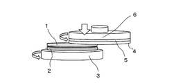
- It is a schematic diagram showing a grinding process for a gallium nitride single crystal.
- FIG. 1 is a plan view showing an example of a carrier in the present disclosure
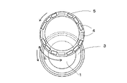
- FIG. FIG. 4 is a plan view schematically showing the positional relationship between the single crystal holder and the wheel-shaped grindstone holder in the surface grinding process.
- 5B is a partial side view of FIG. 5A
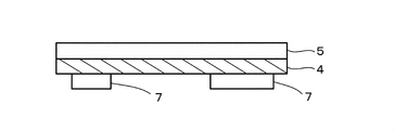
- FIG. FIG. 5 is an explanatory diagram showing the relationship between the gap between adjacent gallium nitride single crystals and the raceway width of the grindstone in the grinding process
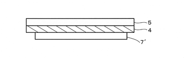
- FIG. 4 is an explanatory diagram showing the relationship between the gallium nitride single crystal and the grindstone track in the grinding process
- 7B is an enlarged view of part A of FIG. 7A.
- FIG. 4 is an explanatory diagram showing the relationship between the gallium nitride single crystal and the grindstone track in the grinding process; It is an enlarged view of the A' part of FIG. 8A.
- 8C is a schematic cross-sectional view of part C1 showing a grindstone track including parts b1 and b2 of FIG. 8B.
- FIG. It is a schematic sectional drawing of the C2 part which shows grindstone track
- FIG. 2 is an explanatory diagram showing an example of a state in which a plurality of gallium nitride single crystals are attached; It is the schematic for demonstrating the prescription
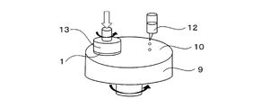
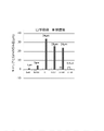
- FIG. 4 is an explanatory view showing ranges A to F of angles to be ground in the surface grinding process; 1 is a schematic diagram showing a CMP process for a gallium nitride single crystal; FIG. It is the graph which investigated the thickness difference of the carrier and the single crystal after grinding
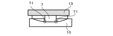
- FIG. 4 is an explanatory diagram for explaining sagging of a single crystal during polishing in a CMP process;
- FIG. 4 is an explanatory diagram for explaining sagging of a single crystal during polishing in a CMP process;
- FIG. 4 is an explanatory diagram for explaining sagging of a single crystal during polishing in a CMP process;
- FIG. 4 is an explanatory diagram for explaining sagging of a single crystal during polishing in a CMP process;
- FIG. 4 is an explanatory diagram for explaining sagging of a single crystal during polishing in a CMP process;
- FIG. 4 is an explanatory diagram for explaining sagging of a single crystal during polishing in a CMP process;
- FIG. 4 is an explanatory diagram for explaining sagging of a single crystal during polishing in a CMP process;
- the Group 13 element nitride crystal substrate means a substrate made of Group 13 element nitride crystal.
- the substrate has a plate-like shape, that is, a shape having a relatively small thickness (for example, 1/10 or less of the width or depth) relative to the width and depth.
- the thirteenth element group nitride crystal is represented by, for example, Ga x Al y In 1-xy N (where 0 ⁇ x ⁇ 1, 0 ⁇ y ⁇ 1), specifically gallium nitride, aluminum nitride , indium nitride, or mixed crystals thereof.
- the “principal surface” of the group 13 element nitride crystal means a surface that is separated in the thickness direction (the direction in which the crystal dimension is smallest) among the surfaces present in the crystal, and the surface (for example, It consists of two surfaces: the device formation surface) and the back surface.
- the surface for example, It consists of two surfaces: the device formation surface
- a gallium nitride single crystal substrate manufacturing method will be described as a representative example, but other group 13 element nitride crystal substrates can be manufactured in the same manner.
- FIG. 1 is a flow chart showing an overview of a gallium nitride single crystal substrate manufacturing method according to an embodiment of the present disclosure.
- a plate-like gallium nitride single crystal 7 (see, for example, FIG. 6; hereinafter sometimes abbreviated as single crystal 7) is prepared.
- a plate-like gallium nitride single crystal 7 having a particular orientation can be obtained by a slicing step of slicing an ingot of gallium nitride single crystal produced by, for example, a vapor phase growth method, with a wire saw or the like.
- an outer shape processing step for processing the outer shape of the single crystal 7 into a desired shape may be performed.
- a gallium nitride single crystal 7 whose main surface is a semipolar plane, a nonpolar plane, or an N plane (nitrogen plane) is used.
- 2A to 2C show the polar plane, semipolar plane and non-polar plane of gallium nitride single crystal 7, respectively.
- a single crystal whose principal plane is a polar plane (the c-plane, ⁇ 0001 ⁇ plane shown in FIG. 2A) has an established growth technique and is a generally used plane.
- a plane perpendicular to the polar plane is a non-polar plane, such as the m-plane ( ⁇ 1-100 ⁇ plane) shown in FIG. 2C.
- ⁇ 11-22 ⁇ plane shown in FIG. 2B ⁇ 11-21 ⁇ plane, ⁇ 11-23 ⁇ plane, ⁇ 30-31 ⁇ plane, ⁇ 20-21 ⁇ plane, ⁇ 10-11 ⁇ plane, ⁇ 10- 12 ⁇ planes, intermediate planes between polar planes and non-polar planes are semipolar planes.
- Gallium nitride single crystal substrates having a semipolar or nonpolar principal surface are expected to be applied to high-efficiency, high-output light-emitting devices.
- the notation of the Miller index is as follows: ( ) indicates a specific plane, ⁇ ⁇ an equivalent plane, [ ] a specific direction, and ⁇ > an equivalent direction.
- azimuths with negative numbers are generally indicated by adding a bar above the number, but in this specification they are indicated by minus (-) for the sake of convenience.
- the ⁇ 0001 ⁇ plane includes the (0001) plane and the (000-1) plane.
- the ⁇ 20-21 ⁇ planes include (20-21) planes, (20-2-1) planes and their equivalents.
- the c-plane grown gallium nitride single crystal is sliced obliquely to the c-plane (so that the main plane is inclined from both the polar plane and the non-polar plane), so that the main plane is a semi-polar plane.
- a plate-shaped gallium nitride single crystal 7 can be cut out.
- by slicing perpendicular to the c-plane it is possible to cut out a plate-like gallium nitride single crystal 7 whose main surface is a non-polar plane.
- the c-plane which is a polar plane, refers to, for example, the (0001) plane and the opposite plane (000-1) plane.
- the c-plane in the group 13 element nitride crystal is the group 13 metal plane or the N plane, and corresponds to the Ga plane or the N plane in gallium nitride (GaN), respectively.
- the plate-shaped single crystal 7 cut out in the slicing step is preferably processed into a desired outer shape by dicing, laser processing, or the like.
- the outer shape (planar shape) of the obtained single crystal 7 is not particularly limited, and may be circular or polygonal. Also, the size is not particularly limited as long as it is plate-like (thickness is relatively small with respect to the size of the main surface).
- the back surface grinding step S2 is mainly performed for processing to a desired thickness, planarization of the back surface, and control of surface roughness. Specifically, it is preferable that the front surface of the single crystal 7 is attached to a base, and the rear surface is ground by, for example, lapping or grindstone grinding. Crystal defects, residual stress, and the like caused by grinding may be removed by etching. As the base, the single crystal holder 2 used in the next step may be used.
- FIGS. 3A and 3B As the grinding apparatus, a vertical axis rotary table type grinding apparatus in which the rotation axis of the chuck table 3 on which the single crystal 7 is placed and the rotation axis of the grindstone holder 5 that holds the grindstone 4 are parallel. It was used.
- the gallium nitride single crystal 7 is attached and held on the surface of the single crystal holder 2 together with the carrier 1 (see FIG. 6).
- a plate-shaped body having a larger area than the single crystal 7 is used as the single crystal holding portion 2, and a plurality of gallium nitride single crystals 7, for example, about three to ten and several, are held on the surface of the single crystal holding portion 2. is preferable for increasing productivity.
- the carrier 1 is a template attached to the single crystal holder 2 together with the gallium nitride single crystal 7 .
- the carrier 1 in this embodiment is, for example, a plate-like body having the shape shown in FIG.
- the opening 11 is a recess or a through hole. An embodiment using a through-hole type opening 11 will be described below.
- the carrier 1 shown in FIG. 3A is held on the surface of the single crystal holder 2 with the gallium nitride single crystals 7 accommodated in the plurality of openings 11 .
- a plurality of openings 11 are arranged annularly along the peripheral edge of the carrier 1 along the circumferential direction.
- the openings 11 may be arranged on a plurality of concentric circles. Moreover, as shown in FIGS. 7B and 8B, there is a tendency that the difference in the grinding direction increases in the width direction (circumferential direction) on the side closer to the center of the carrier 1 within the plane of the single crystal 7 . If the opening 11 is provided near the center of the carrier 1 , it becomes difficult to control the grinding direction by the grindstone 4 . (dimension in the circumferential direction of the carrier 1, in FIG. 6, the long side direction of the rectangle).
- Carrier 1 is made of carbon fiber reinforced plastic (CFRP). Since CFRP has excellent strength, as will be described later, a single carrier 1 can be used in both the grinding and CMP processes, and the trouble of re-bonding the carrier 1 and the reduction in flatness during re-bonding can be avoided. .
- CFRP carbon fiber reinforced plastic
- CFRP uses carbon fiber as a reinforcing material, and thermosetting epoxy resin is mainly used as a base material.
- PC polyphenylene sulfide
- PES polyphenylene sulfide
- PEEK polyetheretherketone
- the single crystal holder 2 for example, a silicon substrate, an alumina ( Al2O3 ) substrate, a sapphire (single crystal alumina) substrate, a silicon carbide (SiC) substrate, or the like can be used.
- an adhesive such as wax or epoxy adhesive, or double-sided tape (adhesive tape with adhesive on both sides) is used.
- the carrier 1 arranged around the gallium nitride single crystal 7 functions as a dummy to be ground together with the gallium nitride single crystal 7, improving the processing accuracy of the end portion.
- the single crystal holder 2 to which the gallium nitride single crystal 7 is attached is placed on the chuck table 3 .
- the chuck table 3 has a surface with a porous structure, and holds the single-crystal holder 2 flat using negative pressure. Also, the chuck table 3 can be rotated about its central axis by a rotation drive source (not shown). Note that the carrier 1 holding the gallium nitride single crystal 7 may be directly held by the chuck table 3 without using the single crystal holder 2 .
- a grindstone 4 (see FIGS. 5A and 5B) for grinding the gallium nitride single crystal 7 is configured, for example, in a rectangular shape and held by a wheel-shaped grindstone holding portion 5 .
- the arrangement of the grindstones 4 on the grindstone holding portion 5 is not particularly limited. , or a disk-shaped or ring-shaped grindstone 4 may be used.
- the elongated grindstone 4 having a long axis and a short axis is arranged with the long axis in the circumferential direction and the short axis in the radial direction. to be placed.
- the diameter (pitch circle diameter of the grindstone 4) of the tracks 8, 8' (see FIGS. 7A, 7B, 8A, 8B) of the grindstone 4 is the width (diameter) of the region where the single crystal 7 is arranged. is greater than or equal to
- the grindstone 4 may have a curved shape with a curvature corresponding to the tracks 8, 8'.
- the whetstone 4 to be used for example, a diamond whetstone, a SiC whetstone, or the like can be used.
- the abrasive grains of the grindstone 4 are not particularly limited as long as they can grind the gallium nitride single crystal 7, but the number is preferably #1000 to #5000.
- the grindstone holding part 5 is fixed to the tip of the spindle 6, and the rotation of the spindle 6 rotates the grindstone holding part 5 in the circumferential direction.
- the single crystal holder 2 and the grindstone holder 5 are arranged to face each other (see FIGS. 3B and 5A). Then, the gallium nitride single crystal 7 and the grindstone 4 are rotated and pressed against each other with a predetermined pressure to grind the main surface of the gallium nitride single crystal 7 .
- the carrier 1 accommodates and holds the gallium nitride single crystal 7 in the peripheral opening 11 shown in FIG. 4, and as shown in FIG. The positional relationship between the portion 2 and the whetstone holding portion 5 is adjusted.
- the chuck table 3 may be tilted with the central portion P as the apex.
- the carrier 1 and the single crystal 7 are deformed following the shape of the chuck table 3, and only a part of the carrier 1 and the single crystal 7 hit the grindstone 4, so that the grinding area can be limited.
- arrow L indicates the grinding area.
- the single crystal holder 2 and the grindstone holder 5 rotate in the same direction, but they may rotate in opposite directions.
- the rotation speed of the chuck table 3 holding the single crystal holder 2 is preferably 50 rpm or more and 500 rpm or less.
- the rotation speed of the grindstone 4 is higher than the rotation speed of the chuck table 3, and the rotation speed (peripheral speed) is preferably 10 m/sec or more and 50 m/sec or less.
- the feeding speed of the grindstone 4 in the thickness direction of the single crystal 7 is preferably 0.01 ⁇ m/second or more and 1.0 ⁇ m/second or less.
- a plurality of openings 11 for accommodating gallium nitride single crystals are provided along the peripheral edge of the carrier 1 (see FIG. 4).
- This can increase productivity.
- wear of the carrier 1 can be reduced.
- the material of the carrier 1 is harder than the single crystal 7 (difficult to grind), it is necessary to increase the machining time or the machining load.
- a carrier 1 having a hardness equal to or less than that of the single crystal 7 (a grinding rate equal to or greater than that) is used to process the single crystal 7 in a state in which the main surface of the single crystal 7 being processed protrudes from the main surface of the carrier 1.
- the gap G between the adjacent openings 11, 11 is preferably equal to or less than the track width W of the grindstone 4.
- there is usually a difference in thickness between the carrier 1 and the single crystal 7 (the single crystal 7 is thicker).
- the gap between the openings 11, 11, that is, the gap G between the main surfaces of the single crystals 7, 7 accommodated in these openings 11, 11, respectively, is larger than the track width W of the grindstone 4,
- the grindstone 4 falls into the gap between the single crystals 7, and the side surface of the grindstone 4 collides with the corner of the single crystal 7, chipping the grindstone 4 or the single crystal 7.
- the gap G means the shortest length separating the openings 11 , 11 .
- the hardness of 1 is preferably equal to or slightly lower than that of single crystal 7 (the grinding rate is equal to or slightly higher than that of single crystal).
- the track width W of the grindstone 4 varies depending on the size of the apparatus and the like, but is preferably about 1 mm to 30 mm, for example.
- the orbit 8 of the grindstone 4 passing through the main surface of the single crystal 7 during one rotation of the grindstone 4 is substantially arcuate.
- the orbit 8 of the grindstone 4 continuously passes through the main surface of one single crystal 7 only once while the grindstone 4 rotates once.
- the track 8 of the grindstone 4 passing through the main surface of one single crystal 7 should be a continuous arc without protruding from the main surface of the single crystal 7 .
- the grindstone 4 passes through the grindstone track 8 only once for any single crystal 7 .
- the grindstone track 8' is cut twice and passes through the main surface of one single crystal 7'. (Refer to part C1 of the grindstone track 8'). That is, it is two times of b1 part and b2 part of FIG. 8B.
- the single crystal 7' extends from the center to the outer side, the grindstone track 8' passes over the main surface of the same single crystal 7' while being cut off twice.
- FIG. 9A is a schematic cross-sectional view of part C1 showing a grinding wheel track 8' including parts b1 and b2 of FIG. 8B
- FIG. 9B is a schematic cross-sectional view of part C2 showing the grinding wheel track 8' of FIG. 8B.
- FIG. 9A when the area ratio of the single crystal 7 in the grindstone 4 is low, the surface pressure applied to the single crystal 7 increases and the grinding speed increases.
- FIG. 9B when the area ratio of the single crystal 7 in the grindstone 4 increases, the surface pressure applied to the single crystal 7 decreases and the grinding speed slows down.
- the workability differs depending on the incident direction (angle) of the grindstone 4, and the surface roughness changes.
- FIG. 10 the case where 18 single crystals 7 having a semipolar plane are attached to the surface of the single crystal holder 2 will be described.
- the arrow indicates the direction of the projection of the [0001] direction (the direction of the gallium plane) of the single crystal 7 onto the main surface.
- the upper side (direction of the arrow) of each single crystal 7 is the side closer to the gallium plane, and the lower side is the side closer to the N plane.
- the grinding direction of the grindstone 4 is the direction M obtained by projecting the [000-1] direction of the single crystal 7 onto the main surface, and the rotation of the single crystal holder 2 and the grindstone holder 5. It is represented by an angle formed with the direction R1 in which the grindstone 4 grinds the main surface.
- the angles formed are 0° to 180° on the upstream side of the rotation direction R2 of the gallium nitride single crystal 7 and 0° to ⁇ 180° on the downstream side.
- the angle formed by the direction in which the grindstone 4 grinds the main surface of the gallium nitride single crystal 7 and the direction in which the c-axis of the gallium nitride single crystal 7 is projected onto the main surface caused nitriding. It was found that there is a difference in the surface roughness of the gallium single crystal 7 (the surface roughness changes depending on the range of angles).
- each gallium nitride single crystal 7 after grinding was classified into the angle ranges A to F shown in FIG. 12 and Table 1 below.
- Each range is represented by the angle formed by the direction of the [000-1] direction of the gallium nitride single crystal 7 projected onto the main surface and the direction in which the grindstone 4 grinds the main surface. 0° to 180° on the side and 0° to -180° on the downstream side.
- the grinding direction of the grindstone 4 was determined from the grinding marks (trajectory of the grindstone 4) formed on the main surface. Table 1 shows the surface roughness for each angle range after grinding.
- the specific processing conditions under which the surface roughness (arithmetic mean height Sa) shown in Table 1 was obtained were as follows: the rotation speed of the chuck table 3 was 100 rpm; ) is 19 m/sec, and the feed speed of the grindstone 4 is 0.12 ⁇ m/sec or less.
- the arithmetic mean height Sa can be determined by, for example, a laser microscope VK-X1100 manufactured by Keyence Corporation.
- the measurement mode is color ultra-depth
- the measurement magnification is 1200 times (objective 50 times, eyepiece 24 times)
- the measurement range is about 60 ⁇ m ⁇ 80 ⁇ m
- the measurement pitch, cutoff filter ⁇ s, and cutoff filter ⁇ c are set to the surface of the measurement area.
- Arithmetic average height Sa is measured at a plurality of points (at least 5 points) by appropriately setting according to the shape, and the average value is used as the measured value.
- the thickness T of the single crystal 7 can be obtained with a micrometer.
- the arithmetic mean height Sa of the gallium nitride single crystal 7 is larger than in the other ranges B, D and F. That is, in the ranges of B, D and F, the main surface is close to a mirror surface, while in the ranges of A, C and E, the arithmetic mean height Sa is 0.2 ⁇ m or more, which is a so-called satin surface. there is In addition, in the ranges A, C and E, the thickness T of the gallium nitride single crystal 7 is smaller than in the other ranges B, D and F (in comparison with the single crystal 7 having almost the same initial thickness, the grinding amount is is larger).
- the surface ground by the grindstone 4 of #3000 is generally satin-finished.
- the main surface of the single crystal 7 ground by the grindstone 4 has an arithmetic average height (Sa) of 0.2 ⁇ m or more, and the grinding process is properly performed. It suggests.
- the main surface of the single crystal 7 ground by the grindstone 4 has an arithmetic mean height (Sa) of less than 0.2 ⁇ m, and the grinding process is not properly performed. (Despite using a grindstone for grinding, it is an abrasive process). In these ranges, it is expected that relatively large residual stress is generated on the machined surface because the grinding process is not performed properly.
- the surface condition of the machined surface is relatively uniform.
- the grinding marks on the main surface of single crystal 7 are formed by a plurality of arcs, and the grinding direction of grindstone 4 changes within the main surface of single crystal 7 .
- the grinding direction of the grindstone 4 (that is, all grinding marks) is within the ranges A, C, and F over the entire area of the main surface, but the grindstone 4 is ground over at least half of the area of the main surface.
- the directions that is, the grinding marks of half or more are in the ranges A, C, and F.
- the arithmetic mean height Sa is larger than in other ranges.
- the surface state of the processed surface is particularly uniform compared to the other ranges. Therefore, it is preferable to perform grinding so that the grinding direction of the grindstone 4 is within the range of A. After finishing the grinding process, the single crystal holder 2 is removed from the chuck table 3 .
- CMP step S4 is shown in FIG.
- CMP is a process for polishing (mirror-finishing) the surface and eliminating fine distortions and the like on the surface.
- FIG. 13 shows the configuration of a CMP processing apparatus. In this apparatus, a polishing pad 10 is provided on the surface of a rotating platen 9, and an alkaline slurry 12 containing abrasive grains is supplied onto the polishing pad 10. As shown in FIG. The carrier 1 containing the gallium nitride single crystal 7 and the single crystal holding part 2 are held on the lower surface of the supporting part 13 after being removed from the chuck table 3 of the grinding apparatus.
- abrasive grains include silica, ceria, titania, zirconia, and alumina.
- Components of the alkaline slurry 12 other than the abrasive grains include, for example, an aqueous sodium hydroxide solution, an aqueous potassium hydroxide solution, and the like.
- the pH of the slurry 12 is preferably adjusted to 8 or more and 14 or less.
- the rotating direction of the polishing pad 10 and the rotating direction of the supporting portion 13 are the same in FIG. 13, they may be opposite directions.
- the slurry 12 may be dropped all the time during the polishing process, or may be dropped intermittently.
- the carbon fiber reinforced plastic (CFRP) that constitutes the carrier 1 has a high polishing resistance against the alkaline slurry 12, so it is hardly polished during CMP processing, and the thickness changes little.
- the carrier 1 containing silicon (Si), such as glass fiber reinforced plastic (GFRP) is subjected to CMP processing using the alkaline slurry 12, the thickness difference from the single crystal 7 becomes large.
- FIG. 14 shows various carrier materials, after grinding in the surface grinding step (S3) in which the carrier 1 and the single crystal 7 are ground together, and using an alkaline slurry 12, the carrier 1 and the single crystal 7 are ground.
- 4 is a graph showing the difference in thickness between the carrier 1 and the single crystal 7 after polishing in the CMP step (S4) of co-grinding and polishing.
- CFRP had a small thickness difference of 0.5 ⁇ m, especially in the CMP process.
- CFRP had a small variation in thickness after grinding and after polishing.
- the thickness difference between the single crystal 7 after the co-grinding process and the carrier 1 is 0 ⁇ m or more and 3 ⁇ m or less (the grinding rate is the same as that of the single crystal 7). can be equal to or slightly larger).
- the thickness difference between the single crystal 7 after the CMP process (after polishing) and the carrier 1 is -1 ⁇ m or more and 1 ⁇ m or less (that is, the polishing rate of the carrier 1 and the single crystal 7 is approximately the same).
- the carrier 1 is made of a material that has a thickness difference of more than 1 ⁇ m after co-shaving and polishing (it is easier to polish than the single crystal 7), the manufacturing cost increases due to a decrease in processing accuracy and a decrease in the number of times the carrier 1 can be used. Become. Using a carrier 1 having a thickness difference smaller than ⁇ 1 ⁇ m after co-grinding (which is harder to polish than the single crystal 7) causes a decrease in processing accuracy and a decrease in processing rate. Therefore, if the carrier 1 is made of a material having a thickness difference of -1 ⁇ m or more and 1 ⁇ m or less after co-shaving and polishing, high-precision and low-cost processing becomes possible.
- the thickness difference after co-shaving and polishing is 0 ⁇ m or more, a relatively high polishing rate can be obtained.
- the use of the carrier 1 of the present embodiment is not limited to co-grinding.
- FIG. 15 is an explanatory diagram for explaining the drooping of the single crystal 7 during polishing in the CMP process. As shown in FIG. 15A, the carrier 1 containing the single crystal 7 in the opening 11 is pressed against the polishing pad 10 by the supporting portion 13 and polished while being rotated.
- the carrier 1 is made of a material such as Si that is easily polished, a thickness difference occurs between the carrier 1' and the single crystal 7, as shown in FIG. 15B1.
- the pressure tends to concentrate on the end portion 71 of the single crystal 7 . Therefore, the single crystal substrate 141 obtained by polishing the single crystal 7 has a large amount of polishing at the end portion 71 as shown in FIG.
- the carrier 1 is made of CFRP, there is almost no thickness difference between the carrier 1 and the single crystal 7. Therefore, as shown in FIG. As shown in FIG. 15C2, the single-crystal substrate 14 obtained by polishing maintains the flatness even at the end portion 71 thereof.
- the carrier 1 is made of CFRP, the carrier 1 can be used repeatedly, which has the advantage of reducing manufacturing costs.
- the distance d from the outer edge 15 of the carrier 1 is preferably 2 mm or more. Since the opening 11 is separated from the outer edge 15 of the carrier 1 by 2 mm or more in this way, the pressure is dispersed by the carrier 1 also at the end 71 near the outer edge of the carrier 1, and the drooping of the end 71 is suppressed. 15B2 and 15C2, the pressure is distributed over the entire single crystal 7, and the flatness of the edge 71 of the single crystal substrate 14 obtained by polishing can be maintained.
- the carrier 1 usually has a disk shape with a diameter of 50 mm or more and 300 mm or less, the carrier 1 is not limited to a disk shape, and may be polygonal such as a square.
- CFRP which has a grinding speed close to that of the substrate material (group 13 element nitride crystal) and is resistant to CMP alkaline slurry.
- the same carrier 1 can be used from the grinding process to the CMP process. As a result, productivity and processing accuracy can be improved, and manufacturing costs can be reduced.
- Reference Signs List 1 1' carrier 11 opening 15 outer edge 2 single crystal holder 3 chuck table 4 grindstone 5 grindstone holder 6 spindle 7 single crystal (periodic table group 13 element nitride crystal) 71 end portion 8 grindstone track 9 surface plate 10 polishing pad 11 opening 12 alkaline slurry 13 supporting portion 14, 141 single crystal substrate (periodic table group 13 element nitride crystal substrate)
Landscapes
- Engineering & Computer Science (AREA)
- Chemical & Material Sciences (AREA)
- Mechanical Engineering (AREA)
- Crystallography & Structural Chemistry (AREA)
- Materials Engineering (AREA)
- Metallurgy (AREA)
- Organic Chemistry (AREA)
- Inorganic Chemistry (AREA)
- Ceramic Engineering (AREA)
- Crystals, And After-Treatments Of Crystals (AREA)
- Mechanical Treatment Of Semiconductor (AREA)
- Grinding Of Cylindrical And Plane Surfaces (AREA)
Priority Applications (2)
| Application Number | Priority Date | Filing Date | Title |
|---|---|---|---|
| US18/574,699 US20240293912A1 (en) | 2021-06-30 | 2022-06-29 | Manufacturing method for manufacturing substrate of nitride crystal of group 13 element in periodic table |
| JP2023532039A JP7650355B2 (ja) | 2021-06-30 | 2022-06-29 | 周期表第13族元素窒化物結晶基板の製造方法 |
Applications Claiming Priority (2)
| Application Number | Priority Date | Filing Date | Title |
|---|---|---|---|
| JP2021-109059 | 2021-06-30 | ||
| JP2021109059 | 2021-06-30 |
Publications (1)
| Publication Number | Publication Date |
|---|---|
| WO2023277103A1 true WO2023277103A1 (ja) | 2023-01-05 |
Family
ID=84691818
Family Applications (1)
| Application Number | Title | Priority Date | Filing Date |
|---|---|---|---|
| PCT/JP2022/026095 Ceased WO2023277103A1 (ja) | 2021-06-30 | 2022-06-29 | 周期表第13族元素窒化物結晶基板の製造方法 |
Country Status (3)
| Country | Link |
|---|---|
| US (1) | US20240293912A1 (https=) |
| JP (1) | JP7650355B2 (https=) |
| WO (1) | WO2023277103A1 (https=) |
Cited By (1)
| Publication number | Priority date | Publication date | Assignee | Title |
|---|---|---|---|---|
| WO2025263587A1 (ja) * | 2024-06-21 | 2025-12-26 | 三桜工業株式会社 | GaN基板及びGaN基板の表面加工方法 |
Citations (8)
| Publication number | Priority date | Publication date | Assignee | Title |
|---|---|---|---|---|
| US20040235402A1 (en) * | 2003-05-20 | 2004-11-25 | Memc Electronic Materials, Inc. | Wafer carrier |
| JP2005510072A (ja) * | 2001-11-20 | 2005-04-14 | レンセラール ポリテクニック インスティチュート | 基板表面を研磨するための方法 |
| WO2015050218A1 (ja) * | 2013-10-02 | 2015-04-09 | 日本碍子株式会社 | 研磨物の製造方法 |
| WO2017010166A1 (ja) * | 2015-07-14 | 2017-01-19 | 三菱化学株式会社 | 非極性または半極性GaNウエハ |
| JP2017098322A (ja) * | 2015-11-19 | 2017-06-01 | 株式会社岡本工作機械製作所 | 研磨装置およびそれを用いたGaN基板の研磨加工方法 |
| JP2018070415A (ja) * | 2016-10-31 | 2018-05-10 | 三菱ケミカル株式会社 | GaNウエハの製造方法 |
| CN109866084A (zh) * | 2019-04-08 | 2019-06-11 | 北京建筑大学 | 一种uv光催化辅助化学机械抛光装置及抛光方法 |
| JP2019162706A (ja) * | 2018-03-20 | 2019-09-26 | 株式会社東京精密 | 研磨装置 |
Family Cites Families (4)
| Publication number | Priority date | Publication date | Assignee | Title |
|---|---|---|---|---|
| JP4207976B2 (ja) * | 2006-05-17 | 2009-01-14 | 住友電気工業株式会社 | 化合物半導体基板の表面処理方法、および化合物半導体結晶の製造方法 |
| JP2009272380A (ja) * | 2008-05-01 | 2009-11-19 | Sumitomo Electric Ind Ltd | Iii族窒化物結晶およびその表面処理方法、iii族窒化物積層体およびその製造方法、ならびにiii族窒化物半導体デバイスおよびその製造方法 |
| JP5966524B2 (ja) * | 2012-03-30 | 2016-08-10 | 三菱化学株式会社 | 第13族窒化物結晶基板の製造方法 |
| JP6280678B1 (ja) * | 2016-12-22 | 2018-02-14 | 三井金属鉱業株式会社 | 研摩液及び研摩方法 |
-
2022
- 2022-06-29 US US18/574,699 patent/US20240293912A1/en active Pending
- 2022-06-29 JP JP2023532039A patent/JP7650355B2/ja active Active
- 2022-06-29 WO PCT/JP2022/026095 patent/WO2023277103A1/ja not_active Ceased
Patent Citations (8)
| Publication number | Priority date | Publication date | Assignee | Title |
|---|---|---|---|---|
| JP2005510072A (ja) * | 2001-11-20 | 2005-04-14 | レンセラール ポリテクニック インスティチュート | 基板表面を研磨するための方法 |
| US20040235402A1 (en) * | 2003-05-20 | 2004-11-25 | Memc Electronic Materials, Inc. | Wafer carrier |
| WO2015050218A1 (ja) * | 2013-10-02 | 2015-04-09 | 日本碍子株式会社 | 研磨物の製造方法 |
| WO2017010166A1 (ja) * | 2015-07-14 | 2017-01-19 | 三菱化学株式会社 | 非極性または半極性GaNウエハ |
| JP2017098322A (ja) * | 2015-11-19 | 2017-06-01 | 株式会社岡本工作機械製作所 | 研磨装置およびそれを用いたGaN基板の研磨加工方法 |
| JP2018070415A (ja) * | 2016-10-31 | 2018-05-10 | 三菱ケミカル株式会社 | GaNウエハの製造方法 |
| JP2019162706A (ja) * | 2018-03-20 | 2019-09-26 | 株式会社東京精密 | 研磨装置 |
| CN109866084A (zh) * | 2019-04-08 | 2019-06-11 | 北京建筑大学 | 一种uv光催化辅助化学机械抛光装置及抛光方法 |
Cited By (1)
| Publication number | Priority date | Publication date | Assignee | Title |
|---|---|---|---|---|
| WO2025263587A1 (ja) * | 2024-06-21 | 2025-12-26 | 三桜工業株式会社 | GaN基板及びGaN基板の表面加工方法 |
Also Published As
| Publication number | Publication date |
|---|---|
| JPWO2023277103A1 (https=) | 2023-01-05 |
| US20240293912A1 (en) | 2024-09-05 |
| JP7650355B2 (ja) | 2025-03-24 |
Similar Documents
| Publication | Publication Date | Title |
|---|---|---|
| JP5743962B2 (ja) | サファイア基板の研削方法 | |
| CA2673660C (en) | Sapphire substrates and methods of making same | |
| US8455879B2 (en) | Sapphire substrates and methods of making same | |
| US9464365B2 (en) | Sapphire substrate | |
| CA2690791C (en) | Methods of crystallographically reorienting single crystal bodies | |
| WO2023277103A1 (ja) | 周期表第13族元素窒化物結晶基板の製造方法 | |
| JP7150199B1 (ja) | 窒化ガリウム単結晶基板の製造方法および周期表第13族元素窒化物単結晶基板の製造方法 | |
| JP2006315136A (ja) | サファイア研削用カップ型回転砥石 |
Legal Events
| Date | Code | Title | Description |
|---|---|---|---|
| 121 | Ep: the epo has been informed by wipo that ep was designated in this application |
Ref document number: 22833249 Country of ref document: EP Kind code of ref document: A1 |
|
| WWE | Wipo information: entry into national phase |
Ref document number: 2023532039 Country of ref document: JP |
|
| WWE | Wipo information: entry into national phase |
Ref document number: 18574699 Country of ref document: US |
|
| NENP | Non-entry into the national phase |
Ref country code: DE |
|
| 122 | Ep: pct application non-entry in european phase |
Ref document number: 22833249 Country of ref document: EP Kind code of ref document: A1 |