WO2023276955A1 - Capteur de pliage - Google Patents
Capteur de pliage Download PDFInfo
- Publication number
- WO2023276955A1 WO2023276955A1 PCT/JP2022/025581 JP2022025581W WO2023276955A1 WO 2023276955 A1 WO2023276955 A1 WO 2023276955A1 JP 2022025581 W JP2022025581 W JP 2022025581W WO 2023276955 A1 WO2023276955 A1 WO 2023276955A1
- Authority
- WO
- WIPO (PCT)
- Prior art keywords
- adhesive
- piezoelectric film
- bending
- main surface
- view
- Prior art date
Links
- 239000000853 adhesive Substances 0.000 claims abstract description 65
- 230000001070 adhesive effect Effects 0.000 claims abstract description 65
- 239000000758 substrate Substances 0.000 claims abstract description 4
- 238000005452 bending Methods 0.000 claims description 59
- 239000000463 material Substances 0.000 claims description 4
- 239000004820 Pressure-sensitive adhesive Substances 0.000 claims 2
- 230000001681 protective effect Effects 0.000 description 8
- 239000004626 polylactic acid Substances 0.000 description 5
- 238000010586 diagram Methods 0.000 description 4
- 229920000747 poly(lactic acid) Polymers 0.000 description 4
- 238000001514 detection method Methods 0.000 description 3
- 230000004048 modification Effects 0.000 description 2
- 238000012986 modification Methods 0.000 description 2
- 239000002033 PVDF binder Substances 0.000 description 1
- 238000005336 cracking Methods 0.000 description 1
- 230000010365 information processing Effects 0.000 description 1
- 230000010354 integration Effects 0.000 description 1
- 229920000642 polymer Polymers 0.000 description 1
- 238000004088 simulation Methods 0.000 description 1
Images


Classifications
-
- G—PHYSICS
- G01—MEASURING; TESTING
- G01B—MEASURING LENGTH, THICKNESS OR SIMILAR LINEAR DIMENSIONS; MEASURING ANGLES; MEASURING AREAS; MEASURING IRREGULARITIES OF SURFACES OR CONTOURS
- G01B7/00—Measuring arrangements characterised by the use of electric or magnetic techniques
- G01B7/30—Measuring arrangements characterised by the use of electric or magnetic techniques for measuring angles or tapers; for testing the alignment of axes
-
- G—PHYSICS
- G01—MEASURING; TESTING
- G01B—MEASURING LENGTH, THICKNESS OR SIMILAR LINEAR DIMENSIONS; MEASURING ANGLES; MEASURING AREAS; MEASURING IRREGULARITIES OF SURFACES OR CONTOURS
- G01B7/00—Measuring arrangements characterised by the use of electric or magnetic techniques
- G01B7/16—Measuring arrangements characterised by the use of electric or magnetic techniques for measuring the deformation in a solid, e.g. by resistance strain gauge
-
- G—PHYSICS
- G01—MEASURING; TESTING
- G01L—MEASURING FORCE, STRESS, TORQUE, WORK, MECHANICAL POWER, MECHANICAL EFFICIENCY, OR FLUID PRESSURE
- G01L1/00—Measuring force or stress, in general
- G01L1/16—Measuring force or stress, in general using properties of piezoelectric devices
-
- G—PHYSICS
- G06—COMPUTING; CALCULATING OR COUNTING
- G06F—ELECTRIC DIGITAL DATA PROCESSING
- G06F1/00—Details not covered by groups G06F3/00 - G06F13/00 and G06F21/00
- G06F1/16—Constructional details or arrangements
- G06F1/1613—Constructional details or arrangements for portable computers
- G06F1/1615—Constructional details or arrangements for portable computers with several enclosures having relative motions, each enclosure supporting at least one I/O or computing function
- G06F1/1616—Constructional details or arrangements for portable computers with several enclosures having relative motions, each enclosure supporting at least one I/O or computing function with folding flat displays, e.g. laptop computers or notebooks having a clamshell configuration, with body parts pivoting to an open position around an axis parallel to the plane they define in closed position
-
- G—PHYSICS
- G06—COMPUTING; CALCULATING OR COUNTING
- G06F—ELECTRIC DIGITAL DATA PROCESSING
- G06F1/00—Details not covered by groups G06F3/00 - G06F13/00 and G06F21/00
- G06F1/16—Constructional details or arrangements
- G06F1/1613—Constructional details or arrangements for portable computers
- G06F1/1633—Constructional details or arrangements of portable computers not specific to the type of enclosures covered by groups G06F1/1615 - G06F1/1626
- G06F1/1637—Details related to the display arrangement, including those related to the mounting of the display in the housing
- G06F1/1652—Details related to the display arrangement, including those related to the mounting of the display in the housing the display being flexible, e.g. mimicking a sheet of paper, or rollable
-
- G—PHYSICS
- G06—COMPUTING; CALCULATING OR COUNTING
- G06F—ELECTRIC DIGITAL DATA PROCESSING
- G06F1/00—Details not covered by groups G06F3/00 - G06F13/00 and G06F21/00
- G06F1/16—Constructional details or arrangements
- G06F1/1613—Constructional details or arrangements for portable computers
- G06F1/1633—Constructional details or arrangements of portable computers not specific to the type of enclosures covered by groups G06F1/1615 - G06F1/1626
- G06F1/1675—Miscellaneous details related to the relative movement between the different enclosures or enclosure parts
- G06F1/1677—Miscellaneous details related to the relative movement between the different enclosures or enclosure parts for detecting open or closed state or particular intermediate positions assumed by movable parts of the enclosure, e.g. detection of display lid position with respect to main body in a laptop, detection of opening of the cover of battery compartment
Definitions
- One embodiment of the present invention relates to a bending sensor.
- FIG. 2B of Patent Document 1 discloses a piezoelectric panel in which an adhesive is arranged on both main surfaces of a piezoelectric film.
- the piezoelectric panel of Patent Literature 1 is used, for example, as a touch sensor.
- an object of an embodiment of the present invention is to provide a bend sensor that prevents stress concentration and cracks in a bendable device.
- a bending sensor includes a piezoelectric film and an adhesive that is arranged on the main surface of the piezoelectric film and adheres the piezoelectric film to a bendable base material. At least a portion of the end face of the piezoelectric film that is bent together with the substrate is covered with the adhesive.
- stress concentration can be prevented and cracks can be prevented in a bendable device.
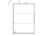
- FIG. 1A is a perspective view of an electronic device 100 having a bending sensor 1
- FIG. 1B is a perspective view of the electronic device 100 in a bent state.
- 1 is a schematic cross-sectional view of an electronic device 100
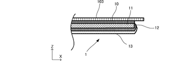
- FIG. 2 is a partially enlarged cross-sectional view of the bending sensor 1
- FIG. 4 is a plan view showing a mother sheet before cutting out the piezoelectric film 11.
- FIG. 5A is a diagram showing strain distribution according to a reference example
- FIG. 5B is a diagram showing strain distribution according to this embodiment.
- 2 is a partially enlarged cross-sectional view of the bending sensor 1;
- FIG. It is a partial expanded sectional view of bending sensor 1 concerning a modification.
- 2 is a plan view of the bending sensor 1;
- FIG. 4 is a plan view showing a mother sheet before cutting out the piezoelectric film 11.
- FIG. 1 is a schematic cross-sectional view of an electronic device 100
- FIG. 2 is
- a bending sensor 1 according to an embodiment of the present invention and an electronic device 100 including the bending sensor 1 will be described below with reference to the drawings.
- electrodes, wiring, etc. are omitted for ease of explanation.
- FIG. 1(A) is a perspective view of an electronic device 100 having a bending sensor 1.
- FIG. 1B is a perspective view of the electronic device 100 in a folded state.
- the electronic device 100 is, for example, an information processing device such as a smart phone.
- FIG. 2 is a schematic cross-sectional view of the electronic device 100 shown in FIG. 1(A) taken along line II shown in FIG. 1(A).
- the bending sensor 1 is enlarged for explanation, and other electronic components are omitted.
- the electronic device 100 includes a substantially rectangular parallelepiped housing 102 .
- the electronic device 100 includes a flat surface panel 103 arranged in a housing 102 .
- the front panel 103 functions as an operation surface on which a user performs a touch operation using a finger, pen, or the like.
- the width direction (horizontal direction) of the housing 102 is defined as the X direction
- the length direction (vertical direction) is defined as the Y direction
- the thickness direction is defined as the Z direction.
- the electronic device 100 has the bending sensor 1 inside the housing 102 .
- the bending sensor 1 is attached to the surface of the surface panel 103 that is inside the housing 102 .
- a bending sensor 1 includes an adhesive 10 , a piezoelectric film 11 , an adhesive 12 and a protective film 13 .
- the bending sensor 1 is attached to the surface panel 103 of the electronic device 100 with the adhesive 10 .
- the bending sensor 1 may be attached to a display device, a touch sensor, or the like. If the bending sensor 1 is transparent, the bending sensor 1 may be arranged closer to the surface panel 103 than the display.
- the housing 102, the surface panel 103, and the bending sensor 1 have flexibility. Thereby, the electronic device 100 can be bent.
- the electronic device 100 can be bent in a predetermined range around the bending line L parallel to the X direction as the bending point L1.
- the surface panel 103 is bent inside, but the surface panel 103 may be bent outside.
- the electronic device 100 can be opened and closed from 0° to 180°.
- the bending sensor 1 detects the presence or absence of bending of the electronic device 100 and the bending state (current opening/closing angle). Note that the electronic device 100 may be made bendable by providing a hinge or a bellows structure at the bending portion.
- the piezoelectric film 11 of the bending sensor 1 is formed in a rectangular shape in plan view.
- the adhesive 10 , the adhesive 12 , and the protective film 13 are in the form of flat films, and are formed in a rectangular shape in plan view, like the piezoelectric film 11 .
- the piezoelectric film 11 is made of a chiral polymer such as PVDF (polyvinylidene fluoride) or polylactic acid.
- Polylactic acid (PLA) may be either L-type polylactic acid (PLLA) or D-type polylactic acid (PDLA).
- the piezoelectric film 11 is polarized when the electronic device 100 is bent and expanded and contracted in the planar direction, and a potential difference is generated between the first main surface and the second main surface.
- Electrodes are formed on both main surfaces of the piezoelectric film 11 . These electrodes are connected to a voltage detection circuit (not shown). A voltage detection circuit detects the potential difference between the electrodes on both main surfaces. A computing unit (not shown) connected to the voltage detection circuit detects bending of the surface panel 103 as a base material when the potential difference (voltage) exceeds a predetermined value. The computing unit can also detect the bending state (opening/closing angle) of the surface panel 103 by performing computation such as integration on the voltage.
- FIG. 3 is a partially enlarged sectional view of the bending sensor 1.
- FIG. The housing 102 is omitted in FIG.
- the main surface of piezoelectric film 11 has a first main surface and a second main surface.
- the adhesive 12, which is the first adhesive is attached to the first main surface
- the adhesive 10, which is the second adhesive is attached to the second main surface along the Z direction.
- a protective film 13 is attached to the first main surface via an adhesive 12 .
- a surface panel 103 is attached to the second main surface via an adhesive 10 .
- the protective film 13 is not an essential component in this embodiment. In this case, the adhesive 12 is also unnecessary.
- FIG. 4 is a plan view showing the mother sheet before the piezoelectric film 11 is cut out.
- the piezoelectric film 11 is cut into individual pieces from the mother sheet shown in FIG. 4 with a pinnacle blade or the like.
- the piezoelectric film 11 is cut by a pinnacle blade from the second main surface side.
- the cross section of the adhesive 10 arranged on the second main surface extends along the X-direction end face of the piezoelectric film 11 by the pinnacle blade, and covers the end face of the piezoelectric film 11 .
- the adhesive 10 relieves strain and relieves stress. Therefore, the adhesive 10 prevents concentration of stress on the X-direction end surface of the bending portion L ⁇ b>1 of the piezoelectric film 11 .
- FIG. 5(A) is a diagram showing strain distribution according to a reference example
- FIG. 5(B) is a diagram showing strain distribution according to this embodiment.
- the strain distribution of the reference example is a simulation when the end face of the piezoelectric film is not covered with the adhesive.
- strain is concentrated near the end face in the X direction at the bending location L1.
- the strain is dispersed, and large strain does not occur in the vicinity of the end surface in the X direction at the bending portion L1.
- the bending sensor 1 of the present embodiment can prevent stress from concentrating on the piezoelectric film 11 in a bendable device, and can prevent the piezoelectric film 11 from cracking.
- FIG. 3 shows an example in which the end surface of the piezoelectric film 11 is covered with the adhesive 10 on the second main surface side.
- the end surfaces of the piezoelectric film 11 may be covered with the adhesive 12 on the first main surface side.
- FIG. 6 is a partially enlarged sectional view of the bending sensor 1.
- the end faces of the piezoelectric film 11 may be covered with the adhesive 12 on the first main surface side.
- the piezoelectric film 11 is cut with a pinnacle blade from the first main surface side.
- the cross section of the adhesive 12 arranged on the first main surface extends along the X-direction end face of the piezoelectric film 11 by the pinnacle blade, and covers the end face of the piezoelectric film 11 .
- the end surface of the piezoelectric film 11 may be further covered with the protective film 13 .
- the end faces of the piezoelectric film 11 are also protected by the protective film 13 .
- FIG. 7 is a partially enlarged cross-sectional view of the bending sensor 1 according to the modification.
- adhesive 10 and adhesive 12 are in contact with each other.
- the X-direction end face of the piezoelectric film 11 is completely covered with the adhesive 12 .
- the adhesive 12 extends along the end surface of the piezoelectric film 11 and contacts the adhesive 10, but the second main surface is cut. If the piezoelectric film 11 is cut from the side, the adhesive 10 will extend along the end face of the piezoelectric film 11 and come into contact with the adhesive 12 . Thereby, the bending sensor 1 can further prevent stress concentration.
- FIG. 8 is a plan view of the bending sensor 1.
- FIG. FIG. 9 is a plan view showing the mother sheet before the piezoelectric film 11 is cut out. In the piezoelectric film 11 shown in FIG. 9, the length along the X direction at the central portion in the Y direction is shorter than the length along the X direction at the end portions in the Y direction.
- the first adhesive and the second adhesive In order to bring the first adhesive and the second adhesive into contact as shown in FIG. 7, for example, as shown in the plan views of FIGS. Alternatively, it may be smaller than the area of the adhesive 12). Thereby, when the piezoelectric film 11 is cut out from the mother sheet, the first adhesive and the second adhesive come into contact with each other.
- the length of the piezoelectric film 11 along the X direction is the same as the X direction of the adhesive 10 (or adhesive 12) at most locations other than the ends in the Y direction. shorter than along the However, the piezoelectric film 11 only has to be shorter in the X direction than the adhesive 10 (or the adhesive 12) at least at the bending portion L1. That is, in the piezoelectric film 11, the length of the first direction (X direction) along the bending line at the bending point L1 in plan view is longer than the length of the adhesive (the adhesive 10 or the adhesive 12) in the first direction. It should have been shorter.
- the bending sensor 1 can further prevent stress concentration.
- the length of the piezoelectric film in the X direction at the bending point L1 is preferably shorter than the length of the adhesive in the X direction by 4% or more.
- the inventors have found that by making the length of the piezoelectric film in the X direction at the bending point L1 shorter by 4% or more than the length of the adhesive in the X direction, stress concentration can be prevented and cracks can be prevented. I confirmed that it is possible.
- both end surfaces in the X direction of the piezoelectric film 11 are covered with an adhesive.
- stress concentration can be prevented if at least one end face in the X direction of the piezoelectric film 11 is covered with an adhesive.
- Reference Signs List 1 bending sensor 10: adhesive 11: piezoelectric film 12: adhesive 13: protective film 100: electronic device 102: housing 103: surface panel
Landscapes
- Engineering & Computer Science (AREA)
- Physics & Mathematics (AREA)
- General Physics & Mathematics (AREA)
- Computer Hardware Design (AREA)
- Theoretical Computer Science (AREA)
- Human Computer Interaction (AREA)
- General Engineering & Computer Science (AREA)
- Mathematical Physics (AREA)
- Force Measurement Appropriate To Specific Purposes (AREA)
- Measurement Of Length, Angles, Or The Like Using Electric Or Magnetic Means (AREA)
Abstract
Un capteur de pliage (1) comprend un film piézoélectrique (11), et un adhésif (10) qui est disposé sur une surface principale du film piézoélectrique (11), et qui fixe le film piézoélectrique (11) à un substrat pliable (103). Au moins une partie de pliage d'une surface de bord du film piézoélectrique (11) qui est pliée conjointement avec le substrat (103) est recouverte par l'adhésif (10).
Priority Applications (3)
| Application Number | Priority Date | Filing Date | Title |
|---|---|---|---|
| JP2023531942A JP7473084B2 (ja) | 2021-06-30 | 2022-06-27 | 曲げセンサ |
| CN202280026764.0A CN117120818A (zh) | 2021-06-30 | 2022-06-27 | 弯曲传感器 |
| US18/491,717 US20240053134A1 (en) | 2021-06-30 | 2023-10-20 | Bending sensor |
Applications Claiming Priority (2)
| Application Number | Priority Date | Filing Date | Title |
|---|---|---|---|
| JP2021-108331 | 2021-06-30 | ||
| JP2021108331 | 2021-06-30 |
Related Child Applications (1)
| Application Number | Title | Priority Date | Filing Date |
|---|---|---|---|
| US18/491,717 Continuation US20240053134A1 (en) | 2021-06-30 | 2023-10-20 | Bending sensor |
Publications (1)
| Publication Number | Publication Date |
|---|---|
| WO2023276955A1 true WO2023276955A1 (fr) | 2023-01-05 |
Family
ID=84689934
Family Applications (1)
| Application Number | Title | Priority Date | Filing Date |
|---|---|---|---|
| PCT/JP2022/025581 WO2023276955A1 (fr) | 2021-06-30 | 2022-06-27 | Capteur de pliage |
Country Status (4)
| Country | Link |
|---|---|
| US (1) | US20240053134A1 (fr) |
| JP (1) | JP7473084B2 (fr) |
| CN (1) | CN117120818A (fr) |
| WO (1) | WO2023276955A1 (fr) |
Citations (6)
| Publication number | Priority date | Publication date | Assignee | Title |
|---|---|---|---|---|
| JPH06174407A (ja) * | 1992-12-03 | 1994-06-24 | Toyo Kako Kk | 角度センサ |
| US20120055257A1 (en) * | 2010-09-08 | 2012-03-08 | Micropen Technologies Corporation | Pressure sensing or force generating device |
| JP2015015018A (ja) * | 2013-06-07 | 2015-01-22 | 株式会社半導体エネルギー研究所 | 情報処理装置、プログラム |
| WO2019021856A1 (fr) * | 2017-07-26 | 2019-01-31 | 株式会社村田製作所 | Appareil électronique |
| JP2021043171A (ja) * | 2019-09-13 | 2021-03-18 | 株式会社ジャパンディスプレイ | 圧電センサ及び圧電センサの製造方法 |
| CN113838373A (zh) * | 2021-08-20 | 2021-12-24 | 京东方科技集团股份有限公司 | 显示面板、检测方法和显示装置 |
-
2022
- 2022-06-27 JP JP2023531942A patent/JP7473084B2/ja active Active
- 2022-06-27 CN CN202280026764.0A patent/CN117120818A/zh active Pending
- 2022-06-27 WO PCT/JP2022/025581 patent/WO2023276955A1/fr active Application Filing
-
2023
- 2023-10-20 US US18/491,717 patent/US20240053134A1/en active Pending
Patent Citations (6)
| Publication number | Priority date | Publication date | Assignee | Title |
|---|---|---|---|---|
| JPH06174407A (ja) * | 1992-12-03 | 1994-06-24 | Toyo Kako Kk | 角度センサ |
| US20120055257A1 (en) * | 2010-09-08 | 2012-03-08 | Micropen Technologies Corporation | Pressure sensing or force generating device |
| JP2015015018A (ja) * | 2013-06-07 | 2015-01-22 | 株式会社半導体エネルギー研究所 | 情報処理装置、プログラム |
| WO2019021856A1 (fr) * | 2017-07-26 | 2019-01-31 | 株式会社村田製作所 | Appareil électronique |
| JP2021043171A (ja) * | 2019-09-13 | 2021-03-18 | 株式会社ジャパンディスプレイ | 圧電センサ及び圧電センサの製造方法 |
| CN113838373A (zh) * | 2021-08-20 | 2021-12-24 | 京东方科技集团股份有限公司 | 显示面板、检测方法和显示装置 |
Also Published As
| Publication number | Publication date |
|---|---|
| JPWO2023276955A1 (fr) | 2023-01-05 |
| US20240053134A1 (en) | 2024-02-15 |
| CN117120818A (zh) | 2023-11-24 |
| JP7473084B2 (ja) | 2024-04-23 |
Similar Documents
| Publication | Publication Date | Title |
|---|---|---|
| US9519378B2 (en) | Pressure detector and touch panel provided with pressure detector | |
| US10248232B2 (en) | Press sensor and electronic device | |
| JP5897055B2 (ja) | 感圧センサ及びタッチパネル | |
| US11487362B1 (en) | Enclosure with locally-flexible regions | |
| JP6278708B2 (ja) | タッチパネル | |
| KR20180078316A (ko) | 정전 용량식 센서 | |
| WO2016027603A1 (fr) | Terminal d'entrée | |
| US10739923B2 (en) | Touch panel member | |
| JP6624343B2 (ja) | センサ、タッチパネル、及び電子機器 | |
| JP7006842B2 (ja) | 押圧センサ | |
| WO2023276955A1 (fr) | Capteur de pliage | |
| JP5804213B2 (ja) | 変位検出センサおよび操作入力装置 | |
| US20120305377A1 (en) | Cover glass pressure button | |
| JP6791456B2 (ja) | 変位検出センサおよびフレキシブルデバイス | |
| WO2021261548A1 (fr) | Capteur piézoélectrique et dispositif électronique | |
| JP6780424B2 (ja) | 押圧力検知センサおよび電子機器 | |
| KR20180078315A (ko) | 정전 용량식 센서 | |
| JP6638560B2 (ja) | 変形検知センサおよび電子機器 | |
| JP2017107478A (ja) | 折曲検知可能なタッチセンサおよび折曲検知可能な表示装置 | |
| JP2019032885A (ja) | 折曲検知可能なタッチセンサおよび折曲検知可能な表示装置 | |
| JP6915746B2 (ja) | 変形センサ、タッチパネル、および表示装置 | |
| JP2023091157A (ja) | 電子機器 | |
| CN114822238A (zh) | 数字化仪 | |
| JPWO2019044800A1 (ja) | タッチパネル |
Legal Events
| Date | Code | Title | Description |
|---|---|---|---|
| 121 | Ep: the epo has been informed by wipo that ep was designated in this application |
Ref document number: 22833102 Country of ref document: EP Kind code of ref document: A1 |
|
| WWE | Wipo information: entry into national phase |
Ref document number: 2023531942 Country of ref document: JP |
|
| NENP | Non-entry into the national phase |
Ref country code: DE |