WO2023276943A1 - 半導体装置 - Google Patents
半導体装置 Download PDFInfo
- Publication number
- WO2023276943A1 WO2023276943A1 PCT/JP2022/025550 JP2022025550W WO2023276943A1 WO 2023276943 A1 WO2023276943 A1 WO 2023276943A1 JP 2022025550 W JP2022025550 W JP 2022025550W WO 2023276943 A1 WO2023276943 A1 WO 2023276943A1
- Authority
- WO
- WIPO (PCT)
- Prior art keywords
- semiconductor device
- metal
- wire
- lead
- semiconductor element
- Prior art date
- Legal status (The legal status is an assumption and is not a legal conclusion. Google has not performed a legal analysis and makes no representation as to the accuracy of the status listed.)
- Ceased
Links
Images








Classifications
-
- H—ELECTRICITY
- H10—SEMICONDUCTOR DEVICES; ELECTRIC SOLID-STATE DEVICES NOT OTHERWISE PROVIDED FOR
- H10W—GENERIC PACKAGES, INTERCONNECTIONS, CONNECTORS OR OTHER CONSTRUCTIONAL DETAILS OF DEVICES COVERED BY CLASS H10
- H10W70/00—Package substrates; Interposers; Redistribution layers [RDL]
- H10W70/40—Leadframes
- H10W70/411—Chip-supporting parts, e.g. die pads
- H10W70/415—Leadframe inner leads serving as die pads
-
- H—ELECTRICITY
- H10—SEMICONDUCTOR DEVICES; ELECTRIC SOLID-STATE DEVICES NOT OTHERWISE PROVIDED FOR
- H10W—GENERIC PACKAGES, INTERCONNECTIONS, CONNECTORS OR OTHER CONSTRUCTIONAL DETAILS OF DEVICES COVERED BY CLASS H10
- H10W70/00—Package substrates; Interposers; Redistribution layers [RDL]
- H10W70/40—Leadframes
- H10W70/481—Leadframes for devices being provided for in groups H10D8/00 - H10D48/00
-
- H—ELECTRICITY
- H10—SEMICONDUCTOR DEVICES; ELECTRIC SOLID-STATE DEVICES NOT OTHERWISE PROVIDED FOR
- H10W—GENERIC PACKAGES, INTERCONNECTIONS, CONNECTORS OR OTHER CONSTRUCTIONAL DETAILS OF DEVICES COVERED BY CLASS H10
- H10W70/00—Package substrates; Interposers; Redistribution layers [RDL]
- H10W70/40—Leadframes
- H10W70/421—Shapes or dispositions
- H10W70/424—Cross-sectional shapes
- H10W70/427—Bent parts
-
- H—ELECTRICITY
- H10—SEMICONDUCTOR DEVICES; ELECTRIC SOLID-STATE DEVICES NOT OTHERWISE PROVIDED FOR
- H10W—GENERIC PACKAGES, INTERCONNECTIONS, CONNECTORS OR OTHER CONSTRUCTIONAL DETAILS OF DEVICES COVERED BY CLASS H10
- H10W70/00—Package substrates; Interposers; Redistribution layers [RDL]
- H10W70/40—Leadframes
- H10W70/464—Additional interconnections in combination with leadframes
- H10W70/465—Bumps or wires
-
- H—ELECTRICITY
- H10—SEMICONDUCTOR DEVICES; ELECTRIC SOLID-STATE DEVICES NOT OTHERWISE PROVIDED FOR
- H10W—GENERIC PACKAGES, INTERCONNECTIONS, CONNECTORS OR OTHER CONSTRUCTIONAL DETAILS OF DEVICES COVERED BY CLASS H10
- H10W70/00—Package substrates; Interposers; Redistribution layers [RDL]
- H10W70/40—Leadframes
- H10W70/464—Additional interconnections in combination with leadframes
- H10W70/466—Tape carriers or flat leads
-
- H—ELECTRICITY
- H10—SEMICONDUCTOR DEVICES; ELECTRIC SOLID-STATE DEVICES NOT OTHERWISE PROVIDED FOR
- H10W—GENERIC PACKAGES, INTERCONNECTIONS, CONNECTORS OR OTHER CONSTRUCTIONAL DETAILS OF DEVICES COVERED BY CLASS H10
- H10W72/00—Interconnections or connectors in packages
- H10W72/071—Connecting or disconnecting
-
- H—ELECTRICITY
- H10—SEMICONDUCTOR DEVICES; ELECTRIC SOLID-STATE DEVICES NOT OTHERWISE PROVIDED FOR
- H10W—GENERIC PACKAGES, INTERCONNECTIONS, CONNECTORS OR OTHER CONSTRUCTIONAL DETAILS OF DEVICES COVERED BY CLASS H10
- H10W72/00—Interconnections or connectors in packages
- H10W72/50—Bond wires
-
- H—ELECTRICITY
- H10—SEMICONDUCTOR DEVICES; ELECTRIC SOLID-STATE DEVICES NOT OTHERWISE PROVIDED FOR
- H10W—GENERIC PACKAGES, INTERCONNECTIONS, CONNECTORS OR OTHER CONSTRUCTIONAL DETAILS OF DEVICES COVERED BY CLASS H10
- H10W72/00—Interconnections or connectors in packages
- H10W72/50—Bond wires
- H10W72/521—Structures or relative sizes of bond wires
- H10W72/522—Multilayered bond wires, e.g. having a coating concentric around a core
-
- H—ELECTRICITY
- H10—SEMICONDUCTOR DEVICES; ELECTRIC SOLID-STATE DEVICES NOT OTHERWISE PROVIDED FOR
- H10W—GENERIC PACKAGES, INTERCONNECTIONS, CONNECTORS OR OTHER CONSTRUCTIONAL DETAILS OF DEVICES COVERED BY CLASS H10
- H10W72/00—Interconnections or connectors in packages
- H10W72/50—Bond wires
- H10W72/551—Materials of bond wires
- H10W72/552—Materials of bond wires comprising metals or metalloids, e.g. silver
- H10W72/5525—Materials of bond wires comprising metals or metalloids, e.g. silver comprising copper [Cu]
-
- H—ELECTRICITY
- H10—SEMICONDUCTOR DEVICES; ELECTRIC SOLID-STATE DEVICES NOT OTHERWISE PROVIDED FOR
- H10W—GENERIC PACKAGES, INTERCONNECTIONS, CONNECTORS OR OTHER CONSTRUCTIONAL DETAILS OF DEVICES COVERED BY CLASS H10
- H10W72/00—Interconnections or connectors in packages
- H10W72/50—Bond wires
- H10W72/551—Materials of bond wires
- H10W72/552—Materials of bond wires comprising metals or metalloids, e.g. silver
- H10W72/5527—Eutectic alloys
-
- H—ELECTRICITY
- H10—SEMICONDUCTOR DEVICES; ELECTRIC SOLID-STATE DEVICES NOT OTHERWISE PROVIDED FOR
- H10W—GENERIC PACKAGES, INTERCONNECTIONS, CONNECTORS OR OTHER CONSTRUCTIONAL DETAILS OF DEVICES COVERED BY CLASS H10
- H10W72/00—Interconnections or connectors in packages
- H10W72/90—Bond pads, in general
-
- H—ELECTRICITY
- H10—SEMICONDUCTOR DEVICES; ELECTRIC SOLID-STATE DEVICES NOT OTHERWISE PROVIDED FOR
- H10W—GENERIC PACKAGES, INTERCONNECTIONS, CONNECTORS OR OTHER CONSTRUCTIONAL DETAILS OF DEVICES COVERED BY CLASS H10
- H10W74/00—Encapsulations, e.g. protective coatings
- H10W74/10—Encapsulations, e.g. protective coatings characterised by their shape or disposition
- H10W74/111—Encapsulations, e.g. protective coatings characterised by their shape or disposition the semiconductor body being completely enclosed
-
- H—ELECTRICITY
- H10—SEMICONDUCTOR DEVICES; ELECTRIC SOLID-STATE DEVICES NOT OTHERWISE PROVIDED FOR
- H10W—GENERIC PACKAGES, INTERCONNECTIONS, CONNECTORS OR OTHER CONSTRUCTIONAL DETAILS OF DEVICES COVERED BY CLASS H10
- H10W74/00—Encapsulations, e.g. protective coatings
- H10W74/10—Encapsulations, e.g. protective coatings characterised by their shape or disposition
- H10W74/111—Encapsulations, e.g. protective coatings characterised by their shape or disposition the semiconductor body being completely enclosed
- H10W74/127—Encapsulations, e.g. protective coatings characterised by their shape or disposition the semiconductor body being completely enclosed characterised by arrangements for sealing or adhesion
-
- H—ELECTRICITY
- H10—SEMICONDUCTOR DEVICES; ELECTRIC SOLID-STATE DEVICES NOT OTHERWISE PROVIDED FOR
- H10W—GENERIC PACKAGES, INTERCONNECTIONS, CONNECTORS OR OTHER CONSTRUCTIONAL DETAILS OF DEVICES COVERED BY CLASS H10
- H10W90/00—Package configurations
-
- H—ELECTRICITY
- H10—SEMICONDUCTOR DEVICES; ELECTRIC SOLID-STATE DEVICES NOT OTHERWISE PROVIDED FOR
- H10W—GENERIC PACKAGES, INTERCONNECTIONS, CONNECTORS OR OTHER CONSTRUCTIONAL DETAILS OF DEVICES COVERED BY CLASS H10
- H10W42/00—Arrangements for protection of devices
- H10W42/121—Arrangements for protection of devices protecting against mechanical damage
-
- H—ELECTRICITY
- H10—SEMICONDUCTOR DEVICES; ELECTRIC SOLID-STATE DEVICES NOT OTHERWISE PROVIDED FOR
- H10W—GENERIC PACKAGES, INTERCONNECTIONS, CONNECTORS OR OTHER CONSTRUCTIONAL DETAILS OF DEVICES COVERED BY CLASS H10
- H10W72/00—Interconnections or connectors in packages
- H10W72/071—Connecting or disconnecting
- H10W72/075—Connecting or disconnecting of bond wires
- H10W72/07551—Connecting or disconnecting of bond wires characterised by changes in properties of the bond wires during the connecting
- H10W72/07552—Connecting or disconnecting of bond wires characterised by changes in properties of the bond wires during the connecting changes in structures or sizes
-
- H—ELECTRICITY
- H10—SEMICONDUCTOR DEVICES; ELECTRIC SOLID-STATE DEVICES NOT OTHERWISE PROVIDED FOR
- H10W—GENERIC PACKAGES, INTERCONNECTIONS, CONNECTORS OR OTHER CONSTRUCTIONAL DETAILS OF DEVICES COVERED BY CLASS H10
- H10W72/00—Interconnections or connectors in packages
- H10W72/50—Bond wires
- H10W72/521—Structures or relative sizes of bond wires
- H10W72/527—Multiple bond wires having different sizes
-
- H—ELECTRICITY
- H10—SEMICONDUCTOR DEVICES; ELECTRIC SOLID-STATE DEVICES NOT OTHERWISE PROVIDED FOR
- H10W—GENERIC PACKAGES, INTERCONNECTIONS, CONNECTORS OR OTHER CONSTRUCTIONAL DETAILS OF DEVICES COVERED BY CLASS H10
- H10W72/00—Interconnections or connectors in packages
- H10W72/50—Bond wires
- H10W72/531—Shapes of wire connectors
- H10W72/536—Shapes of wire connectors the connected ends being ball-shaped
-
- H—ELECTRICITY
- H10—SEMICONDUCTOR DEVICES; ELECTRIC SOLID-STATE DEVICES NOT OTHERWISE PROVIDED FOR
- H10W—GENERIC PACKAGES, INTERCONNECTIONS, CONNECTORS OR OTHER CONSTRUCTIONAL DETAILS OF DEVICES COVERED BY CLASS H10
- H10W72/00—Interconnections or connectors in packages
- H10W72/50—Bond wires
- H10W72/531—Shapes of wire connectors
- H10W72/5363—Shapes of wire connectors the connected ends being wedge-shaped
-
- H—ELECTRICITY
- H10—SEMICONDUCTOR DEVICES; ELECTRIC SOLID-STATE DEVICES NOT OTHERWISE PROVIDED FOR
- H10W—GENERIC PACKAGES, INTERCONNECTIONS, CONNECTORS OR OTHER CONSTRUCTIONAL DETAILS OF DEVICES COVERED BY CLASS H10
- H10W72/00—Interconnections or connectors in packages
- H10W72/50—Bond wires
- H10W72/541—Dispositions of bond wires
- H10W72/5449—Dispositions of bond wires not being orthogonal to a side surface of the chip, e.g. fan-out arrangements
-
- H—ELECTRICITY
- H10—SEMICONDUCTOR DEVICES; ELECTRIC SOLID-STATE DEVICES NOT OTHERWISE PROVIDED FOR
- H10W—GENERIC PACKAGES, INTERCONNECTIONS, CONNECTORS OR OTHER CONSTRUCTIONAL DETAILS OF DEVICES COVERED BY CLASS H10
- H10W72/00—Interconnections or connectors in packages
- H10W72/90—Bond pads, in general
- H10W72/931—Shapes of bond pads
- H10W72/932—Plan-view shape, i.e. in top view
-
- H—ELECTRICITY
- H10—SEMICONDUCTOR DEVICES; ELECTRIC SOLID-STATE DEVICES NOT OTHERWISE PROVIDED FOR
- H10W—GENERIC PACKAGES, INTERCONNECTIONS, CONNECTORS OR OTHER CONSTRUCTIONAL DETAILS OF DEVICES COVERED BY CLASS H10
- H10W74/00—Encapsulations, e.g. protective coatings
-
- H—ELECTRICITY
- H10—SEMICONDUCTOR DEVICES; ELECTRIC SOLID-STATE DEVICES NOT OTHERWISE PROVIDED FOR
- H10W—GENERIC PACKAGES, INTERCONNECTIONS, CONNECTORS OR OTHER CONSTRUCTIONAL DETAILS OF DEVICES COVERED BY CLASS H10
- H10W76/00—Containers; Fillings or auxiliary members therefor; Seals
- H10W76/10—Containers or parts thereof
-
- H—ELECTRICITY
- H10—SEMICONDUCTOR DEVICES; ELECTRIC SOLID-STATE DEVICES NOT OTHERWISE PROVIDED FOR
- H10W—GENERIC PACKAGES, INTERCONNECTIONS, CONNECTORS OR OTHER CONSTRUCTIONAL DETAILS OF DEVICES COVERED BY CLASS H10
- H10W90/00—Package configurations
- H10W90/701—Package configurations characterised by the relative positions of pads or connectors relative to package parts
- H10W90/751—Package configurations characterised by the relative positions of pads or connectors relative to package parts of bond wires
- H10W90/754—Package configurations characterised by the relative positions of pads or connectors relative to package parts of bond wires between a chip and a stacked insulating package substrate, interposer or RDL
-
- H—ELECTRICITY
- H10—SEMICONDUCTOR DEVICES; ELECTRIC SOLID-STATE DEVICES NOT OTHERWISE PROVIDED FOR
- H10W—GENERIC PACKAGES, INTERCONNECTIONS, CONNECTORS OR OTHER CONSTRUCTIONAL DETAILS OF DEVICES COVERED BY CLASS H10
- H10W90/00—Package configurations
- H10W90/701—Package configurations characterised by the relative positions of pads or connectors relative to package parts
- H10W90/751—Package configurations characterised by the relative positions of pads or connectors relative to package parts of bond wires
- H10W90/756—Package configurations characterised by the relative positions of pads or connectors relative to package parts of bond wires between a chip and a stacked lead frame, conducting package substrate or heat sink
-
- H—ELECTRICITY
- H10—SEMICONDUCTOR DEVICES; ELECTRIC SOLID-STATE DEVICES NOT OTHERWISE PROVIDED FOR
- H10W—GENERIC PACKAGES, INTERCONNECTIONS, CONNECTORS OR OTHER CONSTRUCTIONAL DETAILS OF DEVICES COVERED BY CLASS H10
- H10W90/00—Package configurations
- H10W90/701—Package configurations characterised by the relative positions of pads or connectors relative to package parts
- H10W90/791—Package configurations characterised by the relative positions of pads or connectors relative to package parts of direct-bonded pads
- H10W90/792—Package configurations characterised by the relative positions of pads or connectors relative to package parts of direct-bonded pads between multiple chips
-
- H—ELECTRICITY
- H10—SEMICONDUCTOR DEVICES; ELECTRIC SOLID-STATE DEVICES NOT OTHERWISE PROVIDED FOR
- H10W—GENERIC PACKAGES, INTERCONNECTIONS, CONNECTORS OR OTHER CONSTRUCTIONAL DETAILS OF DEVICES COVERED BY CLASS H10
- H10W90/00—Package configurations
- H10W90/701—Package configurations characterised by the relative positions of pads or connectors relative to package parts
- H10W90/791—Package configurations characterised by the relative positions of pads or connectors relative to package parts of direct-bonded pads
- H10W90/794—Package configurations characterised by the relative positions of pads or connectors relative to package parts of direct-bonded pads between a chip and a stacked insulating package substrate, interposer or RDL
Definitions
- the present disclosure relates to semiconductor devices.
- Patent Document 1 discloses such a semiconductor device.
- the semiconductor device includes a semiconductor element, first to fifth leads, bonding wires, and sealing resin.
- the semiconductor element is mounted on the main surface of the mounting portion of the first lead.
- Each electrode of the semiconductor element and the second to fifth leads are connected by bonding wires, respectively.
- a sealing resin covers a portion of each of the first to fifth leads, the semiconductor element and the bonding wires.
- the sealing resin is made of black epoxy resin.
- the sealing resin contains a sulfur component in order to improve the adhesion with the leads.
- Cu is used as a constituent material of the bonding wire.
- the bonding wires are likely to be corroded by the sulfur component and halogen contained in the sealing resin.
- the surface of the bonding wire is easily oxidized, and the oxide film becomes a factor that inhibits bonding with the lead.
- a method using a bonding wire in which a core material made of Cu is coated with Pd or the like is conceivable.
- the coating film protects the core material made of Cu from the sulfur component and halogen in the sealing resin, and also prevents the core material from being oxidized.
- part of the coating film may be peeled off, leaving a portion where the core material is exposed.
- the Pd in the coating film acts as a catalyst for promoting sulfur corrosion, thereby promoting corrosion.
- the present disclosure has been conceived under the circumstances described above, and one of its objectives is to provide a semiconductor device capable of suppressing corrosion of connection members due to sulfur.
- a semiconductor device provided by the present disclosure includes a semiconductor element, first leads electrically connected to the semiconductor element, and connection members connected to the semiconductor element and the first leads.
- the connection member includes a core portion containing a first material, and a surface layer portion containing a first metal and covering the core portion.
- the first material comprises an alloy of a second metal and at least a third metal, and is more corrosion resistant than the second metal.
- the third metal has the highest composition ratio among the added metals and has a higher atomic number than the second metal.
- the semiconductor device according to the present disclosure can suppress corrosion of connection members due to sulfur.
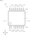
- FIG. 1 is a plan view showing a semiconductor device according to a first embodiment of the present disclosure
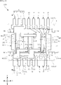
- FIG. FIG. 2 is a plan view of the semiconductor device shown in FIG. 1, and is a view through a resin member.
- 3 is a front view of the semiconductor device shown in FIG. 1.
- FIG. FIG. 4 is a front view of the semiconductor device shown in FIG. 1, and is a view through a resin member.
- 5 is a left side view of the semiconductor device shown in FIG. 1.
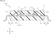
- FIG. FIG. 6 is a cross-sectional view along line VI-VI of FIG. 7 is a partially enlarged view of FIG. 6.
- FIG. 8 is a partially enlarged view of FIG. 6.
- FIG. 9 is a schematic cross-sectional view showing the electronic component according to the first embodiment.
- FIG. 10 is a circuit diagram showing an example of the circuit configuration of the semiconductor device shown in FIG. 1.
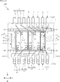
- FIG. FIG. 11 is a plan view showing a semiconductor device according to a second embodiment of the present disclosure, and is a view through a resin member.
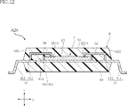
- 12 is a cross-sectional view taken along line XII-XII in FIG. 11.
- FIG. 13 is a partially enlarged view of FIG. 12.
- FIG. 14 is a partially enlarged view of FIG. 12.
- FIG. FIG. 15 is a plan view showing a semiconductor device according to a third embodiment of the present disclosure, and is a view through a resin member.
- FIG. 16 is a plan view showing a semiconductor device according to a fourth embodiment of the present disclosure, and is a view through a resin member.
- FIG. 17 is a plan view showing a semiconductor device according to a fifth embodiment of the present disclosure, and is a view through a resin member.
- a semiconductor device A10 according to the first embodiment of the present disclosure will be described based on FIGS.
- the semiconductor device A10 is surface-mounted on circuit boards of various electronic devices.
- the semiconductor device A10 is a package called SOP (Small Outline Package), for example.
- SOP Small Outline Package
- the package format of the semiconductor device A10 is not limited.
- the semiconductor device A10 is, for example, a power supply IC.
- the application and function of the semiconductor device A10 are not limited.
- the shape of the semiconductor device A10 when viewed in the thickness direction is rectangular (or substantially rectangular). Each dimension of the semiconductor device A10 is not particularly limited.
- a semiconductor device A10 includes an electronic component 1, a conductive support member 4, a connection member 5, and a resin member 6. As shown in FIG.
- FIG. 1 is a plan view showing the semiconductor device A10.
- FIG. 2 is a plan view showing the semiconductor device A10.
- the outline of the resin member 6 is shown by an imaginary line (chain double-dashed line) through the resin member 6 .
- FIG. 3 is a front view showing the semiconductor device A10.
- FIG. 4 is a front view showing the semiconductor device A10.
- the outline of the resin member 6 is shown by an imaginary line (chain double-dashed line) through the resin member 6 .
- Note that the plurality of connection members 5 are omitted in FIG.
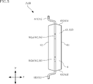
- FIG. 5 is a left side view showing the semiconductor device A10.
- FIG. 6 is a cross-sectional view taken along line VI-VI of FIG. 7 is a partially enlarged view of FIG. 6.
- FIG. 8 is a partially enlarged view of FIG. 6.
- FIG. 9 is a schematic cross-sectional view showing the electronic component 1 (first semiconductor elements 2A and 2B to be described later).
- the thickness direction of the semiconductor device A10 is defined as the z direction
- the direction along one side of the semiconductor device A10 orthogonal to the z direction is defined as the x direction, the z direction, and the x direction.
- the direction perpendicular to the y direction is defined as the y direction.
- one side of the z direction (upper side in the front view shown in FIG. 3) may be referred to as the upper side
- the other side of the z direction (lower side in the front view of FIG. 3) may be referred to as the lower side. It does not limit the posture.
- the electronic component 1 becomes the functional center of the semiconductor device A10.
- the electronic component 1 is bonded to the conductive support member 4 (a die pad 46 to be described later) via a bonding material (not shown).
- the electronic component 1 includes two first semiconductor elements 2A, 2B and a second semiconductor element 3. As shown in FIG.
- Each of the first semiconductor elements 2A, 2B is, for example, a MOSFET (Metal Oxide Semiconductor Field Effect Transistor).
- MOSFET Metal Oxide Semiconductor Field Effect Transistor
- the first semiconductor elements 2A and 2B are not limited to MOSFETs, and may be other transistors such as bipolar transistors or IGBTs (Insulated Gate Bipolar Transistors), or diodes.
- the first semiconductor element 2A includes a semiconductor substrate 21A, a wiring layer 23A, a protective film 24A, and a plurality of electrode pads 251A and 252A (not shown in FIG. 9).
- Semiconductor substrate 21A is made of a semiconductor material such as Si (silicon), SiC (silicon carbide), GaN (gallium nitride), and Ga 2 O 3 (gallium oxide).
- the semiconductor substrate 21A as shown in FIG. 9, has a substrate main surface 211A and a substrate rear surface 212A.
- substrate back surfaces are spaced apart in the z direction.
- the substrate main surface 211A faces upward.
- the substrate back surface 212A faces downward.
- the semiconductor substrate 21A has an active region 220A formed on the main surface 211A side of the substrate.
- Active area 220A includes semiconductor areas 221A, 222A, and 223A.
- the semiconductor region 221A is, for example, a drain region.
- Semiconductor region 222A is, for example, a source region.
- Semiconductor region 223A is, for example, a gate region.
- the wiring layer 23A is formed on the substrate main surface 211A of the semiconductor substrate 21A, as shown in FIG.
- a plurality of conductive layers 231 and a plurality of insulating layers 232 are alternately laminated.
- Each conductive layer 231 is electrically connected through vias 233 formed to penetrate each insulating layer 232 .
- the wiring layer 23A shown in FIG. 9 is an example, and is not limited to this.
- the protective film 24A is formed on the wiring layer 23A and covers the upper surface of the wiring layer 23A. As shown in FIG. 2, the protective film 24A is partially opened, and a plurality of electrode pads 251A and 252A are exposed from the opened portion.
- the protective film 24A is, for example, a Si 3 N 4 layer or SiO 2 layer formed by plasma CVD, or a polyimide resin layer formed by coating. Protective film 24A may be formed by a combination of these.
- a plurality of electrode pads 251A and 252A are terminals of the first semiconductor element 2A.
- Each of the plurality of electrode pads 251A is electrically connected to the semiconductor region 221A via the wiring layer 23A. Therefore, each electrode pad 251A is a drain terminal of the first semiconductor element 2A.
- Each electrode pad 251A is joined to one of the plurality of connection members 5 (wires 51, which will be described later).
- the electrode pad 252A is electrically connected to the semiconductor region 222A through the wiring layer 23A. Therefore, the electrode pad 252A is the source terminal of the first semiconductor element 2A.
- One of the connection members 5 (a wire 53 to be described later) is joined to the electrode pad 252A.
- the first semiconductor element 2B includes a semiconductor substrate 21B, a wiring layer 23B, a protective film 24B and a plurality of electrode pads 251B (not shown in FIG. 9) and 252B.
- Semiconductor substrate 21B is made of a semiconductor material such as Si (silicon), SiC (silicon carbide), GaN (gallium nitride), and Ga 2 O 3 (gallium oxide). As shown in FIG. 9, the semiconductor substrate 21B has a substrate main surface 211B and a substrate back surface 212B. The substrate main surface 211B and the substrate back surface 212B are separated in the z-direction. The substrate main surface 211B faces upward. The substrate back surface 212B faces downward.
- Si silicon
- SiC silicon carbide
- GaN gallium nitride
- Ga 2 O 3 gallium oxide
- the semiconductor substrate 21B has an active region 220B formed on the side of the main surface 211B of the substrate.
- Active region 220B includes semiconductor regions 221B, 222B, and 223B.
- Semiconductor region 221B is, for example, a drain region.
- Semiconductor region 222B is, for example, a source region.
- Semiconductor region 223B is, for example, a gate region.
- the wiring layer 23B is formed on the substrate main surface 211B of the semiconductor substrate 21B, as shown in FIG.
- the wiring layer 23B is configured similarly to the wiring layer 23A. That is, in the wiring layer 23B, for example, a plurality of conductive layers 231 and a plurality of insulating layers 232 are alternately laminated. Each conductive layer 231 is electrically connected through vias 233 formed to penetrate each insulating layer 232 .
- the wiring layer 23B shown in FIG. 9 is an example, and is not limited to this.
- the protective film 24B is formed on the wiring layer 23B and covers the upper surface of the wiring layer 23B. As shown in FIG. 2, the protective film 24B is partially opened, and a plurality of electrode pads 251B and 252B are exposed from the opened portion.
- Protective film 24B is, for example, a Si 3 N 4 layer or SiO 2 layer formed by plasma CVD, or a polyimide resin layer formed by coating. Protective film 24B may be formed by a combination of these. In addition, the protective film 24A and the protective film 24B may be integrally formed.
- a plurality of electrode pads 251B and 252B are terminals of the first semiconductor element 2B.
- the electrode pad 251B is electrically connected to the semiconductor region 221B through the wiring layer 23B. Therefore, each electrode pad 251B is a drain terminal of the first semiconductor element 2B.
- One of the connection members 5 (a wire 54 to be described later) is joined to the electrode pad 251B.
- Each of the plurality of electrode pads 252B is electrically connected to the semiconductor region 222B via the wiring layer 23B. Therefore, the electrode pad 252B is the source terminal of the first semiconductor element 2B.
- Each electrode pad 252B is joined to one of the connection members 5 (wires 52 described later).
- the second semiconductor element 3 is, for example, a driving IC.
- the second semiconductor element 3 controls driving of the plurality of first semiconductor elements 2A and 2B.
- the second semiconductor element 3 is electrically connected to each of the first semiconductor elements 2A and 2B.
- the second semiconductor element 3 is electrically connected to the semiconductor region 223A (gate region) of the first semiconductor element 2A, and by outputting a control signal to the semiconductor region 223A (gate region), the first semiconductor element 2A is Control.
- the second semiconductor element 3 is electrically connected to the semiconductor region 223B (gate region) of the first semiconductor element 2B, and by outputting a control signal to the semiconductor region 223B (gate region), the first semiconductor element 2B to control.
- the second semiconductor element 3 has an element main surface 301 facing upward.
- the element main surface 301 is covered with a protective film 32 similar to the protective films 24A and 24B.
- a part of the protective film 32 is opened, and the electrode pad 31 is exposed from the opened part.
- a plurality of electrode pads 31 are formed on the second semiconductor element 3 .
- a plurality of connection members 5 (a plurality of wires 55 to be described later) are bonded to each electrode pad 31 one by one.
- the conductive support member 4 forms a conductive path between the electronic component 1 and the circuit board by mounting the semiconductor device A10 on a circuit board of an electronic device or the like.
- the conductive support member 4 supports the electronic component 1 .
- a constituent material of the conductive support member 4 is, for example, Cu (copper) or a Cu alloy. In addition, the constituent material of the conductive support member 4 is not limited.
- the conductive support member 4 consists of a lead frame formed by stamping or etching a metal plate. The thickness of the conductive support member 4 is, for example, about 0.2 mm.
- the conductive support member 4 includes a lead 41, a lead 42, a lead 43, a lead 44, a plurality of leads 45, and a die pad 46, as shown in FIG. Lead 41, lead 42, lead 43, lead 44, multiple leads 45, and die pad 46 are spaced apart from each other.
- the lead 41 includes two terminal portions 411 and a pad portion 412, as shown in FIG.
- the pad portion 412 has a rectangular shape elongated in the x-direction with a notch at the corner (lower right corner in FIG. 2) in the direction in which the lead 42 is positioned in a plan view.
- the notch is provided so as not to contact the lead 42 . Note that if the lead 42 is not contacted, the notch may not be provided.
- the wire 51 is joined to the pad portion 412 .
- the pad section 412 has a metal layer 49 as shown in FIG.
- the metal layer 49 is positioned above the pad portion 412 (the side to which the wire 51 is bonded).
- the metal layer 49 is in contact with the resin member 6 .
- Metal layer 49 contains Ag, for example, and is formed by plating, for example.
- each terminal portion 411 A part of each terminal portion 411 is exposed from the resin member 6 .
- Each terminal portion 411 is connected to the pad portion 412 at the portion covered with the resin member 6 .
- Each terminal portion 411 is bent in the z direction at the portion exposed from the resin member 6 .
- the surface of each terminal portion 411 may be plated with Sn, for example.
- the lead 42 includes a terminal portion 421 and a pad portion 422, as shown in FIG.
- the pad portion 422 has a rectangular shape elongated in the x direction in plan view.
- the pad portion 422 has a larger dimension in the x direction than the terminal portion 421 in plan view.
- the pad portion 422 is covered with the resin member 6 . None of the plurality of connection members 5 are connected to the pad portion 422 .
- Pad portion 422 is electrically insulated from electronic component 1 .
- a portion of the terminal portion 421 is exposed from the resin member 6 .
- the terminal portion 421 is connected to the pad portion 422 at the portion covered with the resin member 6 .
- the terminal portion 421 bends in the z direction at the portion exposed from the resin member 6 .
- the surface of terminal portion 421 may be plated with Sn, for example.
- the lead 43 includes two terminal portions 431 and a pad portion 432, as shown in FIG.
- the pad portion 432 has a rectangular shape elongated in the x-direction with a notch at the corner (lower left corner in FIG. 2) in the direction where the lead 42 is positioned in a plan view.
- the notch is provided so as not to contact the lead 42 . Note that if the lead 42 is not contacted, the notch may not be provided.
- the wire 52 is joined to the pad portion 432 .
- the pad section 432 has a metal layer 49 .
- the metal layer 49 is positioned above the pad portion 432 (the side to which the wire 52 is bonded).
- each terminal portion 431 A part of each terminal portion 431 is exposed from the resin member 6 .
- Each terminal portion 431 is connected to the pad portion 432 at the portion covered with the resin member 6 .
- Each terminal portion 431 is bent in the z direction at the portion exposed from the resin member 6 .
- the surface of each terminal portion 431 may be plated with Sn, for example.
- the lead 44 includes three terminal portions 441 and pad portions 442, as shown in FIG.
- the pad portion 442 has a rectangular shape elongated in the x direction in plan view.
- the wire 53 and the wire 54 are joined to the pad portion 442 .
- the pad section 442 has a metal layer 49 .
- the metal layer 49 is positioned above the pad portion 442 (the side to which the wires 53 and 54 are joined).
- each terminal portion 441 A part of each terminal portion 441 is exposed from the resin member 6 .
- Each terminal portion 441 is connected to the pad portion 442 at the portion covered with the resin member 6 .
- Each terminal portion 441 is bent in the z direction at the portion exposed from the resin member 6 .
- the surface of each terminal portion 441 may be plated with Sn, for example.
- the plurality of leads 45 includes terminal portions 451 and pad portions 452, as shown in FIG.
- the pad portion 452 has a constricted shape in the y-direction central portion in plan view.
- a wire 55 to be described later is joined to the pad portion 452 .
- the pad section 452 has a metal layer 49 .
- the metal layer 49 is positioned above the pad portion 452 (the side to which the wire 55 is bonded).
- a part of the terminal portion 451 is exposed from the resin member 6 .
- the terminal portion 451 is connected to the pad portion 452 at the portion covered with the resin member 6 .
- the terminal portion 451 is bent in the z direction at the portion exposed from the resin member 6 .
- the surface of terminal portion 451 may be plated with Sn, for example.
- the electronic component 1 is mounted on the die pad 46 .
- the die pad 46 is not electrically connected to the electronic component 1 in this embodiment, it may be configured to be electrically connected to the electronic component 1 .
- the die pad 46 includes a pad portion 461 and a plurality of extension portions 462, as shown in FIG.
- the pad section 461 has a die pad main surface 461a facing upward, as shown in FIG. Electronic component 1 is bonded to the center of die pad main surface 461a.
- a plurality of extending portions 462 each extend from the pad portion 461 .
- An end face 462 a of each extension 462 is exposed from the resin member 6 .
- the back surface of the pad portion 461 facing downward is covered with the resin member 6 , but the back surface may be exposed from the resin member 6 .
- the leads 41, 42, 43, and some of the leads 45 are arranged on one side of the die pad 46 in the y direction in plan view. These terminal portions 411, 421, 431, and 451 overlap each other when viewed in the x direction.
- the leads 44 and other leads 45 are arranged on the other side of the die pad 46 in the y direction in plan view. These terminal portions 441 and 451 overlap each other when viewed in the x direction.
- the terminal portion 411 of the lead 41, the terminal portion 421 of the lead 42, and the terminal portion 431 of the lead 43 are arranged in the x direction in plan view.
- the terminal portion 421 of the lead 42 is sandwiched between the terminal portion 411 of the lead 41 and the terminal portion 431 of the lead 43 in plan view.
- Each of the plurality of connection members 5 conducts the separated members.
- Each connection member 5 establishes electrical continuity between the electronic component 1 (either the first semiconductor element 2A, 2B or the second semiconductor element 3) and the conductive support member 4.
- the plurality of connection members 5 may include those used for electrical continuity within the electronic component 1 (for example, electrical continuity between the first semiconductor elements 2A and 2B and the second semiconductor element 3).
- Each connection member 5 is a linear member having a circular cross section.
- Each connecting member 5 is a so-called bonding wire.
- the plurality of connecting members 5 includes two wires 51, two wires 52, a wire 53, a wire 54, and a plurality of wires 55, as shown in FIG.
- the two wires 51 electrically connect the electrode pads 251A of the first semiconductor element 2A and the pad portions 412 of the leads 41, respectively.
- Each wire 51 has one end joined to each electrode pad 251A and the other end joined to the pad portion 412, as shown in FIG.
- the thickness (wire diameter) of the wire 51 is not limited, but is about ⁇ 15 ⁇ m or more and 50 ⁇ m or less.
- Each wire 51 includes a core portion 51A and a surface layer portion 51B covering the core portion 51A, as shown in FIGS.
- the constituent material of the core portion 51A is an alloy obtained by adding Pt as an additive metal to Cu, which is the main component metal.
- the alloy is an alloy obtained by adding Pt to Cu to improve corrosion resistance to sulfur, and has higher corrosion resistance to sulfur than Cu.
- metal other than Pt may be added to the alloy.
- Pt has the highest composition ratio among the additive metals, and its content is not limited, but is about 50 ppm or more and 300 ppm or less in terms of parts per million by mass.
- the additive metal for improving corrosion resistance to sulfur is not limited to Pt, and other metals may be used.
- the other metal is desirably a metal having an atomic number greater than that of Cu.
- the main component metal of the constituent material of the core portion 51A is not limited to Cu, and may be other metals. Even in this case, the constituent material of the core portion 51A is an alloy obtained by adding an additive metal to the main component metal to improve corrosion resistance to sulfur.
- the thickness of the core portion 51A is not limited, but is about 0.03 ⁇ m or more and 0.30 ⁇ m or less.
- the constituent material of the surface layer portion 51B contains Pd, for example.
- the surface layer portion 51B is provided to protect the core portion 51A from corrosion due to sulfur and halogen, and to prevent oxidation of the core portion 51A. Further, the surface layer portion 51B is in contact with the metal layer 49 of the pad portion 412 of the lead 41, as shown in FIG. Pd, which is the constituent material of the surface layer portion 51B, has a larger bonding area with respect to the metal layer 49 of the pad portion 412 than the constituent material of the core portion 51A (an alloy of Cu and Pt). is high. In other words, the surface layer portion 51B also has a function of increasing the bonding strength between the wire 51 and the lead 41 .
- the constituent material of the surface layer portion 51B is not limited to Pd, and any metal having the above functions may be used.
- each wire 51 has a main portion 511 and an end portion 512 .
- the end portion 512 is interposed between the main portion 511 and the pad portion 412 of the lead 41 .
- End portion 512 has a tapered portion 512A and a tip portion 512B.
- the tapered portion 512A is connected to the main portion 511, and the dimension d in the z direction becomes smaller as the distance from the main portion 511 increases.
- a bonding interface 412A between the pad portion 412 and the wire 51 straddles the main portion 511 and the end portion 512 in a z-direction view (also referred to as a plan view).
- the distal end portion 512B is connected to the tapered portion 512A and protrudes from the tapered portion 512A in the z-direction.
- the wire 51 is formed by wire bonding using a wire material in which a film made of the material of the surface layer part 51B is formed on the surface of the wire material made of the material of the core material part 51A.
- a method for forming a film on the surface of the wire material constituting the wire material includes a plating method, a vapor deposition method, a melting method, and the like, but is not particularly limited.
- the wire 51 is formed, for example, as follows. First, the tip of the wire material is melted to form a ball, and the ball is pressed against the electrode pad 251A of the first semiconductor element 2A for first bonding.
- the surface layer portion 51B melts into the core portion 51A when the ball is formed, the surface portion 51B does not cover the core portion 51A at the portion where the wire 51 is joined to the electrode pad 251A, as shown in FIG. Note that the surface layer portion 51B may partially or entirely cover the core portion 51A depending on the discharge conditions and the type of wire material. In this case, the thickness (dimension in the z-direction) of the joint is reduced.
- the wire material is sent out and pressed against the pad portion 412 of the lead 41 to perform second bonding.
- the end portion 512 is formed by the second bonding.
- the two wires 52 electrically connect the electrode pads 252B of the first semiconductor element 2B and the pad portions 432 of the leads 43, respectively.
- Each wire 52 has one end joined to each electrode pad 252B and the other end joined to the pad portion 432, as shown in FIG.
- the wire 53 electrically connects the electrode pad 252A of the first semiconductor element 2A and the pad portion 442 of the lead 44 .
- the wire 53 has one end joined to the electrode pad 252A and the other end joined to the pad portion 442, as shown in FIG.
- the wire 54 electrically connects the electrode pad 251B of the first semiconductor element 2B and the pad portion 442 of the lead 44 .
- the wire 54 has one end joined to the electrode pad 251B and the other end joined to the pad portion 442, as shown in FIG. Wires 52 to 54 have the same configuration as wire 51 .
- Each of the plurality of wires 55 electrically connects each electrode pad 31 of the second semiconductor element 3 and the pad portion 452 of each lead 45 .
- Each wire 55 has one end joined to each electrode pad 31 and the other end joined to the pad portion 452 of each lead 45, as shown in FIG.
- Each wire 55 does not include a portion corresponding to the surface layer portion 51B of the wire 51, and consists only of a portion corresponding to the core portion 51A.
- the constituent material of the wire 55 is Cu to which no other metal is added.
- the constituent material of the wire 55 is not limited.
- the constituent material of the wire 55 may be a metal (for example, Au) having higher electrical resistivity than Cu, which is the main component metal of the core portion 51A of the wire 51 .
- the thickness (wire diameter) of the plurality of wires 55 is not limited, it is, for example, about ⁇ 15 ⁇ m or more and 50 ⁇ m or less.
- Each wire 51-54 is joined to either the drain terminals (electrode pads 251A, 251B) or the source terminals (electrode pads 252A, 252B) of the first semiconductor elements 2A, 2B. Since relatively large currents flow through these drain and source terminals, relatively large currents also flow through the wires 51-54.
- each wire 55 is joined to each electrode pad 31 of the second semiconductor element 3 . A relatively small current flows through each electrode pad 31 compared to the current flowing through the drain terminal and the source terminal. Therefore, the current flowing through each wire 55 is smaller than the current flowing through each wire 51-54. In general, the higher the current flowing through a wire, the more likely it is that the wire will be corroded by sulfur.
- the wires 51 to 54 through which relatively large currents flow and are likely to be corroded by sulfur, are configured such that the surface layer portion 51B covers the core portion 51A. Also, the wire 55 through which a relatively small current flows does not include a surface layer.
- the resin member 6 covers the electronic component 1, part of the conductive support member 4, and the plurality of connection members 5, respectively.
- the resin member 6 is made of an insulating resin material.
- a constituent material of the resin member 6 is, for example, a black epoxy resin.
- the material and color of the resin member 6 are not limited.
- the resin member 6 contains a sulfur component in order to improve adhesion with the conductive support member 4 .
- the content of sulfur in the resin member 6 is 5 ppm or more and 30 ppm or less in parts per million mass.
- the sulfur content described above can be measured, for example, by the following method.
- a cured product obtained by thermally curing the resin composition of the resin member 6 at 175° C. for 4 hours is pulverized to obtain a pulverized product.
- the resin member 6 has, for example, a rectangular shape in plan view. Resin member 6 is formed, for example, by transfer molding using a mold. In addition, the constituent material, shape, and forming method of the resin member 6 are not limited.
- the resin member 6 has a resin main surface 61 , a resin back surface 62 and a plurality of resin side surfaces 63 .
- the resin main surface 61 and the resin back surface 62 are separated in the z direction.
- the resin main surface 61 is the upper surface of the resin member 6 .
- the resin rear surface 62 is the lower surface of the resin member 6 .
- the plurality of resin side surfaces 63 are connected to both the resin main surface 61 and the resin back surface 62 and are sandwiched between them in the z direction.
- the resin member 6 has a pair of resin side surfaces 631 spaced apart in the x direction and a pair of resin side surfaces 632 spaced apart in the y direction. Each lead 41 to 45 protrudes from one of the pair of resin side surfaces 632 .
- FIG. 10 is a circuit diagram showing an example of the circuit configuration of the semiconductor device A10.
- FIG. 10 is a circuit diagram when the semiconductor device A10 is configured as a DC/DC converter.
- sw1 and sw2 indicate switching elements.
- Dr indicates a control circuit that controls switching operations of the switching elements sw1 and sw2 and various protection function operations.
- R1 to R3 are resistors
- Vref is an internal reference voltage circuit
- ss is a soft start circuit
- pgd is a power good circuit
- amp is an error amplifier that inputs the Vref output voltage and the FB terminal voltage, each shown.
- one of the switching elements sw1 and sw2 corresponds to the first semiconductor element 2A, and the other corresponds to the first semiconductor element 2B.
- the second semiconductor element 3 includes an internal reference voltage circuit Vref, a soft start circuit ss, a power good circuit pgd, an error amplifier amp, and a control circuit Dr.
- the terminal PVIN is the power input terminal of the DC/DC converter.
- the terminal PVIN is connected to a high-potential-side terminal of a DC power supply (not shown).
- the terminal PVIN corresponds to the lead 41 of the semiconductor device A10.
- a terminal PGND is a ground terminal of the DC/DC converter.
- the terminal PGND is connected to a low-potential-side terminal of a DC power supply (not shown).
- a terminal PGND corresponds to the lead 43 of the semiconductor device A10.
- a terminal SW is an output terminal of the DC/DC converter.
- the terminal SW corresponds to the lead 44 of the semiconductor device A10.
- the terminal AVIN is an analog section power supply input terminal.
- a terminal AGND is an analog section ground terminal.
- a terminal EN is a device control terminal.
- a terminal FB is an output voltage feedback terminal.
- a terminal SS is a soft start time setting terminal.
- a terminal COMP is an ERRAMP output terminal.
- Terminal PGD is a power good terminal.
- the terminal CTL is a various function control terminal.
- a terminal MODE may be used instead of the terminal CTL.
- a terminal MODE is a terminal for switching various modes.
- Terminal AVIN, terminal AGND, terminal EN, terminal FB, terminal SS, terminal COMP, terminal PGD, and terminal CTL (or terminal MODE) correspond to one of the plurality of leads 45 one by one.
- a connection line between the terminal PVIN and the drain electrode of the switching element sw1 corresponds to the wire 51
- a connection line between the terminal PGND and the source electrode of the switching element sw2 corresponds to the wire 52
- a connection line between the terminal SW and the source electrode of the switching element sw1 corresponds to the wire 53
- a connection line between the terminal SW and the drain electrode of the switching element sw2 corresponds to the wire .
- Connection lines of other terminals correspond to the wires 55, respectively. Since a large current flows from the terminal PVIN to the terminal PGND in the semiconductor device A10, a large current flows through the wires 51-54. On the other hand, since the current flowing through the other terminals is small, the current flowing through each wire 55 is small.
- the wire 51 includes a core portion 51A and a surface layer portion 51B covering the core portion 51A.
- the constituent material of the surface layer portion 51B contains Pd. Therefore, the surface layer portion 51B can prevent corrosion and oxidation of the core portion 51A and improve the bonding strength of the wire 51 to the lead 41 .
- the constituent material of the core portion 51A is an alloy obtained by adding an additive metal for improving corrosion resistance to sulfur to Cu, which is the main component metal.
- wire 51 has a portion where the surface layer portion 51B is partially peeled off and the core portion 51A is exposed, the corrosion of the core portion 51A due to sulfur can be suppressed.
- Pt is employed as the additive metal. Corrosion of the core portion 51A due to sulfur is thereby appropriately suppressed. The same is true for wires 52-54.
- the wire 55 does not include a portion corresponding to the surface layer portion 51B of the wire 51, and consists only of a portion corresponding to the core portion 51A. Since only a relatively small current flows through wire 55, sulfur corrosion is less likely to be accelerated.
- the semiconductor device A10 has a structure in which only the wires 51 to 54, through which a large amount of current flows and which are likely to be corroded by sulfur, are configured such that the surface layer portion 51B covers the core portion 51A. In this manner, the semiconductor device A10 is appropriately improved in corrosion resistance due to sulfur. If the constituent material of the wire 55 is Cu to which no other metal is added, the cost of the wire 55 can be lower than that of the wires 51-54.
- the semiconductor device A10 can achieve both an improvement in corrosion resistance due to sulfur and a reduction in cost. Further, when the constituent material of the wire 55 is Au, the cost of the semiconductor device A10 can be reduced as compared with the case where the wires 51 to 54 have the same configuration as the wire 55 . In addition, since the main component of the wires 51 to 54 through which a large current flows is Cu, loss due to resistance can be suppressed compared to the case of using Au, which has a higher electrical resistivity than Cu. Therefore, the semiconductor device A10 can achieve both improvement in corrosion resistance due to sulfur and suppression of resistance loss and cost.
- the wire 51 has the core portion 51A covered with the surface layer portion 51B.
- the surface layer portion 51B has a higher bonding strength with the lead 41 than the core portion 51A.
- the semiconductor device A10 can suppress deterioration of the bonding state of the wire 51 to the lead 41 (occurrence of cracks, peeling, etc.). The same is true for wires 52-54.
- the wire 51 has a main portion 511 and an end portion 512 positioned between the main portion 511 and the pad portion 412 .
- the end portion 512 has a tapered portion 512A in which the dimension d (see FIG. 8) in the z direction decreases as the distance from the main portion 511 increases.
- a bonding interface 412A (see FIG. 8) between the pad portion 412 and the wire 51 is provided across the main portion 511 and the end portion 512 as viewed in the z direction.
- the sulfur content of the resin member 6 is 5 ppm or more and 50 ppm or less in parts per million by mass. Since the wires 52 to 54 are highly resistant to corrosion by sulfur as described above, the resin member 6 can contain sulfur to some extent. As a result, the resin member 6 can improve adhesion to the conductive support member 4 while suppressing corrosion of the wires 52 to 54 due to the sulfur component.
- can't Wire 55 may have a structure in which, for example, a core portion made of Cu to which no other metal is added is covered with a surface layer portion similar to surface layer portion 51B of wire 51 . In this case, the bonding strength of the wire 55 to the lead 45 can be improved.
- the semiconductor device A10 includes the wires 51 to 54, which are bonding wires, as the connection member 5 has been described, but the present invention is not limited to this.
- the semiconductor device A10 may include, as the connecting member 5, a wide bonding ribbon having the same configuration as the wires 51 to 54 (including the core portion 51A and the surface layer portion 51B covering the core portion 51A).
- the connection member 5 is not limited to these.
- FIG. 11 to 14 are diagrams for explaining the semiconductor device A20 according to the second embodiment of the present disclosure.
- FIG. 11 is a plan view showing the semiconductor device A20, corresponding to FIG. In FIG. 11 , for convenience of understanding, the outline of the resin member 6 is shown by an imaginary line (chain double-dashed line) through the resin member 6 .
- 12 is a cross-sectional view taken along line XII-XII in FIG. 11.
- FIG. 13 is a partially enlarged view of FIG. 12.
- FIG. 14 is a partially enlarged view of FIG. 12.
- FIG. The semiconductor device A20 according to the present embodiment differs from the semiconductor device A10 according to the first embodiment in that connection leads 56-58 are provided instead of the wires 51-54.
- connection leads 56-58 are provided instead of the wires 51-54.
- the configuration and operation of other portions of this embodiment are the same as those of the first embodiment.
- connection leads 56-58 instead of the wires 51-54.
- the connection leads 56 to 58 electrically connect the first semiconductor elements 2A, 2B and the leads 41, 43, 44 to each other.
- the connection leads 56 to 58 are plate-shaped conductors formed by bending a metal plate. The shape and thickness of the connection leads 56-58 are not limited.
- connection leads 56 electrically connect the electrode pads 251A of the first semiconductor element 2A and the pad portions 412 of the leads 41, as shown in FIGS.
- the connection lead 56 is joined to the electrode pad 251A through a joining material 7 such as solder as shown in FIG. 13, and is joined to the pad portion 412 through the joining material 7 as shown in FIG. ing.
- the connection lead 56 includes a body portion 56A and a surface layer portion 56B covering the body portion 56A.
- the constituent material of the main body portion 56A is an alloy obtained by adding Pt as an additive metal to Cu, which is the main component metal.
- the alloy is an alloy obtained by adding Pt to Cu to improve corrosion resistance to sulfur, and has higher corrosion resistance to sulfur than Cu.
- metal other than Pt may be added to the alloy.
- Pt has the highest composition ratio among the additive metals, and its content is not limited, but is about 50 ppm or more and 300 ppm or less in terms of parts per million by mass.
- the additive metal for improving corrosion resistance to sulfur is not limited to Pt, and other metals may be used.
- the other metal is desirably a metal having an atomic number greater than that of Cu.
- the main component metal of the constituent material of the main body portion 56A is not limited to Cu, and may be other metals. Even in this case, the constituent material of the main body portion 56A is an alloy in which an additive metal is added to improve the corrosion resistance to sulfur to the main component metal.
- the constituent material of the surface layer portion 56B contains Pd, for example.
- the surface layer portion 56B is provided to protect the body portion 56A from corrosion due to sulfur and halogen, and to prevent oxidation of the body portion 56A.
- the constituent material of the surface layer portion 56B is not limited to Pd, and any metal having the above functions may be used.
- the surface layer portion 56B is formed on the surface of the main body portion 56A by plating, for example. Note that the method of forming the connection lead 56 is not limited.
- connection leads 57 electrically connect the electrode pads 252B of the first semiconductor element 2B and the pad portions 432 of the leads 43, as shown in FIG. 11 and 12, the connection lead 58 electrically connects the electrode pad 252A of the first semiconductor element 2A, the electrode pad 251B of the first semiconductor element 2B, and the pad portion 442 of the lead 44. As shown in FIG.
- the configuration of the connection leads 57 and 58 is similar to that of the connection lead 56 .
- connection lead 56 includes a body portion 56A and a surface layer portion 56B covering the body portion 56A.
- the constituent material of the surface layer portion 56B contains Pd. Therefore, the surface layer portion 56B can prevent corrosion and oxidation of the main body portion 56A.
- the constituent material of the main body portion 56A is an alloy in which an additive metal is added to improve corrosion resistance against sulfur to Cu, which is the main component metal.
- connection leads 57 and 58 are the same.
- the wire 55 does not include a portion corresponding to the surface layer portion 51B of the wire 51, and consists only of a portion corresponding to the core portion 51A. Since only a relatively small current flows through wire 55, sulfur corrosion is less likely to be accelerated.
- the semiconductor device A20 employs the connection leads 56 to 58 only for the connection members in which a large current flows and corrosion by sulfur is likely to be accelerated. In this way, the semiconductor device A20 is appropriately improved in corrosion resistance due to sulfur. Moreover, the semiconductor device A20 has the same effect as the semiconductor device A10 due to the configuration common to the semiconductor device A10.
- FIG. 15 is a diagram for explaining the semiconductor device A30 according to the third embodiment of the present disclosure.
- FIG. 15 is a plan view showing the semiconductor device A30, corresponding to FIG. In FIG. 15, for convenience of understanding, the outline of the resin member 6 is shown by an imaginary line (chain double-dashed line) through the resin member 6.
- the semiconductor device A30 according to this embodiment differs from the semiconductor device A10 according to the first embodiment in the configuration of each wire 55 .
- the configuration and operation of other portions of this embodiment are the same as those of the first embodiment. Note that each part of the above first and second embodiments may be combined arbitrarily.
- the wire 55 according to this embodiment has the same configuration as the wire 51 .
- All of the connection members 5 (wires 51 to 55) included in the semiconductor device A30 are configured to include a core portion 51A and a surface layer portion 51B covering the core portion 51A.
- the wires 51 to 55 include a core portion 51A and a surface layer portion 51B covering the core portion 51A.
- the wires 51 to 55 have their core portions 51A protected from corrosion by sulfur and halogen, and can be prevented from being oxidized.
- the constituent material of the surface layer portion 51B contains Pd. Therefore, the surface layer portion 51B can prevent corrosion and oxidation of the core portion 51A and improve the bonding strength of the wires 51 to 55 to the conductive support member 4.
- the constituent material of the core portion 51A is an alloy obtained by adding an additive metal for improving corrosion resistance to sulfur to Cu, which is the main component metal.
- the corrosion of the core portions 51A due to sulfur can be suppressed.
- Pt is employed as the additive metal. Corrosion of the core portion 51A due to sulfur is thereby appropriately suppressed.
- the semiconductor device A30 has the same effect as the semiconductor device A10 due to the configuration common to the semiconductor device A10. Furthermore, according to this embodiment, the wire materials for forming the wires 51 to 55 are all common. In the wire bonding process, it is not necessary to change the wire material and bonding method depending on the wire to be formed, so the manufacturing process can be simplified.
- FIG. 16 is a diagram for explaining a semiconductor device A40 according to the fourth embodiment of the present disclosure.
- FIG. 16 is a plan view showing the semiconductor device A40, corresponding to FIG. In FIG. 16 , for convenience of understanding, the outline of the resin member 960 is shown by an imaginary line (chain double-dashed line) through the resin member 960 .
- a semiconductor device A40 according to the present embodiment differs from the semiconductor device A10 according to the first embodiment in that a semiconductor element 920 is provided instead of the electronic component 1.
- FIG. The configuration and operation of other portions of this embodiment are the same as those of the first embodiment. Note that each part of the above first to third embodiments may be combined arbitrarily.
- the semiconductor device A40 is a package called DFN (Dual Flatpack No-leaded), for example. Note that the package format of the semiconductor device A40 is not limited.
- a semiconductor device A40 includes a semiconductor element 920 in place of the electronic component 1 .
- the semiconductor device A40 also includes leads 941 to 943 as the conductive support member 4, wires 951 and 952 as the connection member 5, and a resin member 960.
- FIG. 1 DFN (Dual Flatpack No-leaded)
- the lead 941 is arranged at the end of the semiconductor device A40 on one side in the y direction (upper side in FIG. 16) and spreads all over in the x direction.
- the lead 942 is arranged at a corner on one side in the x direction (left side in FIG. 16) on the other side in the y direction (lower side in FIG. 16) of the semiconductor device A40.
- the lead 943 is arranged at the corner of the semiconductor device A40 on the other side in the y direction and on the other side in the x direction (on the right side in FIG. 16).
- Leads 942 and 943 are spaced apart from lead 941 in the y-direction and spaced apart from each other in the x-direction.
- Leads 941 support semiconductor element 920 .
- Leads 941 to 943 are each electrically connected to semiconductor element 920 .
- the semiconductor element 920 is, for example, a MOSFET. Note that the semiconductor element 920 may be another transistor such as an IGBT.
- a semiconductor element 920 has a source electrode 921 and a gate electrode 922 arranged on its main surface, and a drain electrode arranged on its back surface.
- a drain electrode of the semiconductor element 920 is conductively connected to a lead 941 via a bonding material. The lead 941 thereby functions as a drain terminal.
- a source electrode 921 of the semiconductor element 920 is conductively connected to a lead 942 via a wire 951 .
- the lead 942 thereby functions as a source terminal.
- a gate electrode 922 of the semiconductor element 920 is conductively connected to a lead 943 via a wire 952 .
- the lead 943 thereby functions as a gate terminal.
- the wire 951 electrically connects the source electrode 921 of the semiconductor element 920 and the lead 942 .
- the wire 951 has one end joined to the source electrode 921 and the other end joined to the lead 942 .
- the wire 951 has the same configuration as the wire 51 according to the first embodiment, and includes a core portion 51A and a surface layer portion 51B covering the core portion 51A.
- a wire 952 electrically connects the gate electrode 922 of the semiconductor element 920 and the lead 943 .
- the wire 952 has one end joined to the gate electrode 922 and the other end joined to the lead 943 .
- the wire 952 has the same configuration as the wire 55 according to the first embodiment. Since a relatively large current flows through the source electrode 921 , a relatively large current also flows through the wire 951 .
- the current flowing through wire 952 is smaller than the current flowing through wire 951 .
- only the wire 951, through which a relatively large current flows and is likely to be corroded by sulfur, is configured such that the surface layer portion 51B covers the core portion 51A.
- the wire 952 through which a relatively small current flows does not include the surface layer.
- the wire 951 includes a core portion 51A and a surface layer portion 51B covering the core portion 51A. This protects the core portion 51A of the wire 951 from corrosion due to sulfur and halogen, and prevents the core portion 51A from being oxidized.
- the constituent material of the surface layer portion 51B contains Pd. Therefore, the surface layer portion 51B can prevent corrosion and oxidation of the core portion 51A and improve the bonding strength of the wire 951 to the lead 942 .
- the constituent material of the core portion 51A is an alloy obtained by adding an additive metal for improving corrosion resistance to sulfur to Cu, which is the main component metal.
- the wire 952 does not include a portion corresponding to the surface layer portion 51B of the wire 951, and consists only of a portion corresponding to the core portion 51A. Since only a relatively small current flows through wire 952, sulfur corrosion is less likely to be accelerated.
- the semiconductor device A40 has a structure in which the surface layer portion 51B only covers the core portion 51A of the wire 951, through which a large current flows and which is easily corroded by sulfur. In this manner, the semiconductor device A40 is appropriately improved in corrosion resistance due to sulfur. If the constituent material of the wire 952 is Cu to which no other metal is added, the cost of the wire 952 can be kept lower than that of the wire 951 .
- the semiconductor device A40 can achieve both an improvement in corrosion resistance due to sulfur and a reduction in cost. Further, when the constituent material of the wire 952 is Au, the cost of the semiconductor device A40 can be reduced more than when the wire 951 and the wire 952 have the same configuration. In addition, since the main component of the wire 951 through which a large current flows is Cu, loss due to resistance can be suppressed compared to the case of using Au, which has a higher electrical resistivity than Cu. Therefore, the semiconductor device A40 can achieve both improvement in corrosion resistance due to sulfur and suppression of resistance loss and cost. In addition, the semiconductor device A40 has the same effect as the semiconductor device A10 due to the configuration common to the semiconductor device A10.
- the semiconductor element 920 is a transistor
- the present invention is not limited to this.
- the type of semiconductor element 920 is not limited.
- the number, shape, and arrangement of each conductive support member 4 are not limited, and the number of each connection member 5 is also not limited.
- FIG. 17 is a diagram for explaining a semiconductor device A50 according to the fifth embodiment of the present disclosure.
- FIG. 17 is a plan view showing the semiconductor device A50, corresponding to FIG. In FIG. 17 , for convenience of understanding, the outline of the resin member 960 is indicated by an imaginary line (chain double-dashed line) through the resin member 960 .
- the semiconductor device A50 according to this embodiment differs from the semiconductor device A10 according to the first embodiment in that it includes a semiconductor element 970 instead of the electronic component 1 .
- the configuration and operation of other portions of this embodiment are the same as those of the first embodiment. It should be noted that each part of the above-described first to fourth embodiments may be combined arbitrarily.
- the semiconductor device A50 includes a semiconductor element 970 instead of the electronic component 1.
- the semiconductor device A50 also includes a lead 944 and a plurality of leads 945 as the conductive support member 4, wires 951 and 952 as the connection member 5, and a resin member 960.
- FIG. 1 A lead 944 and a plurality of leads 945 as the conductive support member 4, wires 951 and 952 as the connection member 5, and a resin member 960.
- the lead 944 is arranged in the center of the semiconductor device A50 in the x direction and spreads over the entirety in the y direction.
- a plurality of leads 945 are arranged on both sides of the lead 944 in the x direction, five of each, at regular intervals in the y direction.
- Each lead 945 is spaced apart from lead 944 and spaced apart from each other.
- Leads 944 support semiconductor element 970 .
- Each lead 945 is electrically connected to the semiconductor element 970 respectively.
- leads 945 include lead 945a and lead 945b.
- Lead 945a is located at the top on the left side in FIG. 17, and lead 945b is located at the bottom on the left side in FIG.
- the semiconductor element 970 is, for example, an LSI ((Large Scale Integration)).
- the semiconductor element 970 may be another electronic component.
- the semiconductor element 970 is bonded to the leads 944 via a bonding material.
- a plurality of electrode pads 971 are arranged on the main surface of the semiconductor element 970.
- the plurality of electrode pads 971 includes an electrode pad 971a and an electrode pad 971b.
- the electrode pad 971a is a power supply electrode.
- the electrode pad 971b is a ground electrode.In the present embodiment, the electrode pad 971a is arranged on the left side of the main surface in FIG. Note that there is no limitation on the arrangement position of each electrode pad 971.
- Electrodes The pad 971a is connected to the lead 945a through the wire 951.
- the lead 945a thus functions as a power terminal
- the electrode pad 971b is connected through the wire 951 to the lead 945b.
- the lead 945b functions as a ground terminal.
- a single wire 951 electrically connects the electrode pad 971a of the semiconductor element 970 and the lead 945a.
- the wire 951 has one end joined to the electrode pad 971a and the other end joined to the lead 945a.
- Another wire 951 electrically connects the electrode pad 971b of the semiconductor element 970 and the lead 945b.
- the wire 951 has one end joined to the electrode pad 971b and the other end joined to the lead 945b.
- Each wire 951 has the same configuration as the wire 51 according to the first embodiment, and includes a core portion 51A and a surface layer portion 51B covering the core portion 51A.
- a plurality of wires 952 electrically connect electrode pads 971 other than electrode pads 971a and 971b and leads 945 other than leads 945a and 945b.
- Each wire 952 has one end joined to the electrode pad 971 and the other end joined to the lead 945 .
- Each wire 952 has the same configuration as the wire 55 according to the first embodiment. Since a relatively large current flows through the electrode pads 971 a and 971 b, a relatively large current also flows through the wire 951 . On the other hand, a relatively small current flows through each of the electrode pads 971 other than the electrode pads 971 a and 971 b , so a relatively small current also flows through the wire 952 . In the present embodiment, only the wire 951, through which a relatively large current flows and is likely to be corroded by sulfur, is configured such that the surface layer portion 51B covers the core portion 51A. On the other hand, the wire 952 through which a relatively small current flows does not include the surface layer.
- the wire 951 includes a core portion 51A and a surface layer portion 51B covering the core portion 51A.
- the constituent material of the surface layer portion 51B contains Pd. Therefore, the surface layer portion 51B can prevent corrosion and oxidation of the core portion 51A and improve the bonding strength of the wire 951 to the leads 945a and 945b.
- the constituent material of the core portion 51A is an alloy obtained by adding an additive metal for improving corrosion resistance to sulfur to Cu, which is the main component metal.
- the wire 952 does not include a portion corresponding to the surface layer portion 51B of the wire 951, and consists only of a portion corresponding to the core portion 51A. Since only a relatively small current flows through wire 952, sulfur corrosion is less likely to be accelerated.
- the semiconductor device A50 has a structure in which the surface layer portion 51B only covers the core portion 51A of the wire 951, through which a large current flows and which is easily corroded by sulfur. In this way, the semiconductor device A50 is appropriately improved in corrosion resistance due to sulfur. If the constituent material of the wire 952 is Cu to which no other metal is added, the cost of the wire 952 can be kept lower than that of the wire 951 .
- the semiconductor device A50 can achieve both an improvement in corrosion resistance due to sulfur and a reduction in cost. Further, when the constituent material of the wire 952 is Au, the cost of the semiconductor device A50 can be reduced more than when the wire 951 and the wire 952 have the same configuration. In addition, since the main component of the wire 951 through which a large current flows is Cu, loss due to resistance can be suppressed compared to the case of using Au, which has a higher electrical resistivity than Cu. Therefore, the semiconductor device A50 can achieve both improvement in corrosion resistance due to sulfur and suppression of resistance loss and cost. Moreover, the semiconductor device A50 has the same effect as the semiconductor device A10 due to the configuration common to the semiconductor device A10.
- the semiconductor element 970 is an LSI
- the present invention is not limited to this.
- the type of semiconductor element 970 is not limited.
- the number, shape, and arrangement of each conductive support member 4 are not limited, and the number of each connection member 5 is also not limited.
- the semiconductor device according to the present disclosure is not limited to the above-described embodiments.
- the specific processing of the specific configuration of each part of the semiconductor device according to the present disclosure can be changed in design in various ways.
- the present disclosure includes embodiments set forth in the following appendices.
- Appendix 1 a semiconductor element (2A); a first lead (41) electrically connected to the semiconductor element; a connection member (51) connected to the semiconductor element and the first lead; with The connecting member includes a core portion (51A) containing a first material, and a surface layer portion (51B) containing a first metal (Pd) and covering the core portion,
- the first material contains an alloy obtained by adding at least a third metal (Pt) to a second metal (Cu), and has higher corrosion resistance than the second metal,
- the semiconductor device according to claim 1 wherein the third metal has the highest composition ratio among the added metals and has a higher atomic number than the second metal.
- Appendix 2. The semiconductor device according to appendix 1, wherein the second metal is Cu. Appendix 3. 3.
- the semiconductor device according to any one of Appendices 1 to 6, wherein the second connecting member is composed only of a second core member containing a second material (Cu).
- Appendix 8. the semiconductor element is a transistor, The semiconductor device according to appendix 7, wherein the second semiconductor element is a driving IC that drives and controls the transistor.
- Appendix 9. (Fourth embodiment, FIG. 16) a second lead (943) electrically connected to the semiconductor element (920); a second connection member (952) connected to the semiconductor element and the second lead and having a small current flowing from the connection member; further comprising 7.
- the semiconductor device according to any one of Appendices 1 to 6, wherein the second connecting member is composed only of a second core member containing a second material.
- Appendix 11. The semiconductor device according to any one of appendices 7 to 10, wherein the second material consists only of the second metal (Cu) to which no other metal is added.
- Appendix 12. 11. The semiconductor device according to any one of appendices 7 to 10, wherein the second material contains a fourth metal (Au) having an electrical resistivity higher than that of the second metal (Cu).
- Appendix 14. Further comprising a resin member (6) covering the connection member, 14.
Landscapes
- Wire Bonding (AREA)
Priority Applications (4)
| Application Number | Priority Date | Filing Date | Title |
|---|---|---|---|
| JP2023531932A JPWO2023276943A1 (https=) | 2021-06-30 | 2022-06-27 | |
| CN202280045503.3A CN117561591A (zh) | 2021-06-30 | 2022-06-27 | 半导体器件 |
| DE112022003353.3T DE112022003353T5 (de) | 2021-06-30 | 2022-06-27 | Halbleitervorrichtung |
| US18/538,483 US20240112988A1 (en) | 2021-06-30 | 2023-12-13 | Semiconductor device |
Applications Claiming Priority (2)
| Application Number | Priority Date | Filing Date | Title |
|---|---|---|---|
| JP2021-108426 | 2021-06-30 | ||
| JP2021108426 | 2021-06-30 |
Related Child Applications (1)
| Application Number | Title | Priority Date | Filing Date |
|---|---|---|---|
| US18/538,483 Continuation US20240112988A1 (en) | 2021-06-30 | 2023-12-13 | Semiconductor device |
Publications (1)
| Publication Number | Publication Date |
|---|---|
| WO2023276943A1 true WO2023276943A1 (ja) | 2023-01-05 |
Family
ID=84689903
Family Applications (1)
| Application Number | Title | Priority Date | Filing Date |
|---|---|---|---|
| PCT/JP2022/025550 Ceased WO2023276943A1 (ja) | 2021-06-30 | 2022-06-27 | 半導体装置 |
Country Status (5)
| Country | Link |
|---|---|
| US (1) | US20240112988A1 (https=) |
| JP (1) | JPWO2023276943A1 (https=) |
| CN (1) | CN117561591A (https=) |
| DE (1) | DE112022003353T5 (https=) |
| WO (1) | WO2023276943A1 (https=) |
Citations (3)
| Publication number | Priority date | Publication date | Assignee | Title |
|---|---|---|---|---|
| JP2011003745A (ja) * | 2009-06-18 | 2011-01-06 | Sumitomo Metal Mining Co Ltd | Cuボンディングワイヤ |
| JP5912008B1 (ja) * | 2015-06-15 | 2016-04-27 | 日鉄住金マイクロメタル株式会社 | 半導体装置用ボンディングワイヤ |
| JP2018078229A (ja) * | 2016-11-11 | 2018-05-17 | 日鉄住金マイクロメタル株式会社 | 半導体装置用ボンディングワイヤ |
Family Cites Families (1)
| Publication number | Priority date | Publication date | Assignee | Title |
|---|---|---|---|---|
| JP2021027116A (ja) | 2019-08-02 | 2021-02-22 | ローム株式会社 | 半導体装置 |
-
2022
- 2022-06-27 DE DE112022003353.3T patent/DE112022003353T5/de active Pending
- 2022-06-27 WO PCT/JP2022/025550 patent/WO2023276943A1/ja not_active Ceased
- 2022-06-27 CN CN202280045503.3A patent/CN117561591A/zh active Pending
- 2022-06-27 JP JP2023531932A patent/JPWO2023276943A1/ja active Pending
-
2023
- 2023-12-13 US US18/538,483 patent/US20240112988A1/en active Pending
Patent Citations (3)
| Publication number | Priority date | Publication date | Assignee | Title |
|---|---|---|---|---|
| JP2011003745A (ja) * | 2009-06-18 | 2011-01-06 | Sumitomo Metal Mining Co Ltd | Cuボンディングワイヤ |
| JP5912008B1 (ja) * | 2015-06-15 | 2016-04-27 | 日鉄住金マイクロメタル株式会社 | 半導体装置用ボンディングワイヤ |
| JP2018078229A (ja) * | 2016-11-11 | 2018-05-17 | 日鉄住金マイクロメタル株式会社 | 半導体装置用ボンディングワイヤ |
Also Published As
| Publication number | Publication date |
|---|---|
| DE112022003353T5 (de) | 2024-04-18 |
| US20240112988A1 (en) | 2024-04-04 |
| CN117561591A (zh) | 2024-02-13 |
| JPWO2023276943A1 (https=) | 2023-01-05 |
Similar Documents
| Publication | Publication Date | Title |
|---|---|---|
| US7675148B2 (en) | Power module having stacked flip-chip and method of fabricating the power module | |
| CN107210241B (zh) | 功率半导体装置 | |
| KR100884675B1 (ko) | 반도체 장치 | |
| JP6685143B2 (ja) | 電極端子、半導体装置及び電力変換装置 | |
| JP7548714B2 (ja) | 電子装置、電子装置の製造方法、およびリードフレーム | |
| US20260053029A1 (en) | Semiconductor device | |
| JP7570391B2 (ja) | 半導体装置 | |
| CN115335984A (zh) | 半导体装置 | |
| JP7579224B2 (ja) | 半導体装置 | |
| WO2023276943A1 (ja) | 半導体装置 | |
| US20230110154A1 (en) | Semiconductor device | |
| JP6064845B2 (ja) | 半導体装置 | |
| WO2022080081A1 (ja) | 半導体装置 | |
| US20250285945A1 (en) | Semiconductor device including a lead and a sealing resin | |
| US20250022822A1 (en) | Semiconductor element and semiconductor device | |
| JP7290960B2 (ja) | 半導体装置 | |
| WO2024157817A1 (ja) | 半導体装置 | |
| JP2026071337A (ja) | 半導体装置 | |
| WO2022168618A1 (ja) | 半導体装置 | |
| WO2023120185A1 (ja) | 半導体装置 | |
| WO2022259809A1 (ja) | 半導体装置 | |
| JP2023072579A (ja) | 半導体装置 |
Legal Events
| Date | Code | Title | Description |
|---|---|---|---|
| 121 | Ep: the epo has been informed by wipo that ep was designated in this application |
Ref document number: 22833090 Country of ref document: EP Kind code of ref document: A1 |
|
| WWE | Wipo information: entry into national phase |
Ref document number: 2023531932 Country of ref document: JP |
|
| WWE | Wipo information: entry into national phase |
Ref document number: 202280045503.3 Country of ref document: CN |
|
| WWE | Wipo information: entry into national phase |
Ref document number: 112022003353 Country of ref document: DE |
|
| 122 | Ep: pct application non-entry in european phase |
Ref document number: 22833090 Country of ref document: EP Kind code of ref document: A1 |