WO2023276854A1 - 照明装置 - Google Patents
照明装置 Download PDFInfo
- Publication number
- WO2023276854A1 WO2023276854A1 PCT/JP2022/025147 JP2022025147W WO2023276854A1 WO 2023276854 A1 WO2023276854 A1 WO 2023276854A1 JP 2022025147 W JP2022025147 W JP 2022025147W WO 2023276854 A1 WO2023276854 A1 WO 2023276854A1
- Authority
- WO
- WIPO (PCT)
- Prior art keywords
- light
- lens
- lighting device
- opening
- optical system
- Prior art date
Links
- 230000003287 optical effect Effects 0.000 claims abstract description 209
- 238000005286 illumination Methods 0.000 claims description 104
- 230000007246 mechanism Effects 0.000 claims description 23
- 125000006850 spacer group Chemical group 0.000 claims description 23
- 238000003384 imaging method Methods 0.000 claims description 14
- 230000009467 reduction Effects 0.000 claims description 13
- 239000010408 film Substances 0.000 description 27
- 239000000463 material Substances 0.000 description 17
- 238000006243 chemical reaction Methods 0.000 description 15
- 230000002093 peripheral effect Effects 0.000 description 15
- 238000009434 installation Methods 0.000 description 13
- 230000004313 glare Effects 0.000 description 12
- 238000011282 treatment Methods 0.000 description 11
- 238000010521 absorption reaction Methods 0.000 description 8
- 230000005284 excitation Effects 0.000 description 8
- 238000009826 distribution Methods 0.000 description 7
- 239000000835 fiber Substances 0.000 description 6
- 238000000034 method Methods 0.000 description 6
- 229910052788 barium Inorganic materials 0.000 description 4
- 229910052751 metal Inorganic materials 0.000 description 4
- 239000002184 metal Substances 0.000 description 4
- 229910052712 strontium Inorganic materials 0.000 description 4
- 238000002834 transmittance Methods 0.000 description 4
- 229910004298 SiO 2 Inorganic materials 0.000 description 3
- GWEVSGVZZGPLCZ-UHFFFAOYSA-N Titan oxide Chemical compound O=[Ti]=O GWEVSGVZZGPLCZ-UHFFFAOYSA-N 0.000 description 3
- 230000001154 acute effect Effects 0.000 description 3
- 238000010586 diagram Methods 0.000 description 3
- 239000003989 dielectric material Substances 0.000 description 3
- 230000006870 function Effects 0.000 description 3
- ORUIBWPALBXDOA-UHFFFAOYSA-L magnesium fluoride Chemical compound [F-].[F-].[Mg+2] ORUIBWPALBXDOA-UHFFFAOYSA-L 0.000 description 3
- ZKATWMILCYLAPD-UHFFFAOYSA-N niobium pentoxide Inorganic materials O=[Nb](=O)O[Nb](=O)=O ZKATWMILCYLAPD-UHFFFAOYSA-N 0.000 description 3
- URLJKFSTXLNXLG-UHFFFAOYSA-N niobium(5+);oxygen(2-) Chemical compound [O-2].[O-2].[O-2].[O-2].[O-2].[Nb+5].[Nb+5] URLJKFSTXLNXLG-UHFFFAOYSA-N 0.000 description 3
- BPUBBGLMJRNUCC-UHFFFAOYSA-N oxygen(2-);tantalum(5+) Chemical compound [O-2].[O-2].[O-2].[O-2].[O-2].[Ta+5].[Ta+5] BPUBBGLMJRNUCC-UHFFFAOYSA-N 0.000 description 3
- 230000008569 process Effects 0.000 description 3
- 239000011347 resin Substances 0.000 description 3
- 229920005989 resin Polymers 0.000 description 3
- 239000000126 substance Substances 0.000 description 3
- 239000000758 substrate Substances 0.000 description 3
- PBCFLUZVCVVTBY-UHFFFAOYSA-N tantalum pentoxide Inorganic materials O=[Ta](=O)O[Ta](=O)=O PBCFLUZVCVVTBY-UHFFFAOYSA-N 0.000 description 3
- 239000010409 thin film Substances 0.000 description 3
- 238000013459 approach Methods 0.000 description 2
- 229910052791 calcium Inorganic materials 0.000 description 2
- 230000008859 change Effects 0.000 description 2
- 238000005253 cladding Methods 0.000 description 2
- 238000004519 manufacturing process Methods 0.000 description 2
- 229910044991 metal oxide Inorganic materials 0.000 description 2
- 150000004706 metal oxides Chemical class 0.000 description 2
- 238000012986 modification Methods 0.000 description 2
- 230000004048 modification Effects 0.000 description 2
- 238000010422 painting Methods 0.000 description 2
- 238000007747 plating Methods 0.000 description 2
- 230000007480 spreading Effects 0.000 description 2
- 238000003892 spreading Methods 0.000 description 2
- 239000004925 Acrylic resin Substances 0.000 description 1
- 229920000178 Acrylic resin Polymers 0.000 description 1
- 229910004283 SiO 4 Inorganic materials 0.000 description 1
- 229910004122 SrSi Inorganic materials 0.000 description 1
- 230000009471 action Effects 0.000 description 1
- 239000000853 adhesive Substances 0.000 description 1
- 230000001070 adhesive effect Effects 0.000 description 1
- 229910052782 aluminium Inorganic materials 0.000 description 1
- 238000003491 array Methods 0.000 description 1
- 230000002238 attenuated effect Effects 0.000 description 1
- 230000002146 bilateral effect Effects 0.000 description 1
- 239000003086 colorant Substances 0.000 description 1
- 229910052802 copper Inorganic materials 0.000 description 1
- 239000004744 fabric Substances 0.000 description 1
- 239000011521 glass Substances 0.000 description 1
- 229910052749 magnesium Inorganic materials 0.000 description 1
- 239000011777 magnesium Substances 0.000 description 1
- 239000005304 optical glass Substances 0.000 description 1
- 239000000123 paper Substances 0.000 description 1
- 238000012545 processing Methods 0.000 description 1
- 238000009877 rendering Methods 0.000 description 1
- 239000004065 semiconductor Substances 0.000 description 1
- 238000012546 transfer Methods 0.000 description 1
- 229910052844 willemite Inorganic materials 0.000 description 1
Images


Classifications
-
- F—MECHANICAL ENGINEERING; LIGHTING; HEATING; WEAPONS; BLASTING
- F21—LIGHTING
- F21S—NON-PORTABLE LIGHTING DEVICES; SYSTEMS THEREOF; VEHICLE LIGHTING DEVICES SPECIALLY ADAPTED FOR VEHICLE EXTERIORS
- F21S8/00—Lighting devices intended for fixed installation
- F21S8/02—Lighting devices intended for fixed installation of recess-mounted type, e.g. downlighters
-
- F—MECHANICAL ENGINEERING; LIGHTING; HEATING; WEAPONS; BLASTING
- F21—LIGHTING
- F21S—NON-PORTABLE LIGHTING DEVICES; SYSTEMS THEREOF; VEHICLE LIGHTING DEVICES SPECIALLY ADAPTED FOR VEHICLE EXTERIORS
- F21S8/00—Lighting devices intended for fixed installation
- F21S8/04—Lighting devices intended for fixed installation intended only for mounting on a ceiling or the like overhead structures
-
- F—MECHANICAL ENGINEERING; LIGHTING; HEATING; WEAPONS; BLASTING
- F21—LIGHTING
- F21V—FUNCTIONAL FEATURES OR DETAILS OF LIGHTING DEVICES OR SYSTEMS THEREOF; STRUCTURAL COMBINATIONS OF LIGHTING DEVICES WITH OTHER ARTICLES, NOT OTHERWISE PROVIDED FOR
- F21V11/00—Screens not covered by groups F21V1/00, F21V3/00, F21V7/00 or F21V9/00
- F21V11/08—Screens not covered by groups F21V1/00, F21V3/00, F21V7/00 or F21V9/00 using diaphragms containing one or more apertures
- F21V11/10—Screens not covered by groups F21V1/00, F21V3/00, F21V7/00 or F21V9/00 using diaphragms containing one or more apertures of iris type
-
- F—MECHANICAL ENGINEERING; LIGHTING; HEATING; WEAPONS; BLASTING
- F21—LIGHTING
- F21V—FUNCTIONAL FEATURES OR DETAILS OF LIGHTING DEVICES OR SYSTEMS THEREOF; STRUCTURAL COMBINATIONS OF LIGHTING DEVICES WITH OTHER ARTICLES, NOT OTHERWISE PROVIDED FOR
- F21V13/00—Producing particular characteristics or distribution of the light emitted by means of a combination of elements specified in two or more of main groups F21V1/00 - F21V11/00
- F21V13/02—Combinations of only two kinds of elements
-
- F—MECHANICAL ENGINEERING; LIGHTING; HEATING; WEAPONS; BLASTING
- F21—LIGHTING
- F21V—FUNCTIONAL FEATURES OR DETAILS OF LIGHTING DEVICES OR SYSTEMS THEREOF; STRUCTURAL COMBINATIONS OF LIGHTING DEVICES WITH OTHER ARTICLES, NOT OTHERWISE PROVIDED FOR
- F21V13/00—Producing particular characteristics or distribution of the light emitted by means of a combination of elements specified in two or more of main groups F21V1/00 - F21V11/00
- F21V13/12—Combinations of only three kinds of elements
-
- F—MECHANICAL ENGINEERING; LIGHTING; HEATING; WEAPONS; BLASTING
- F21—LIGHTING
- F21V—FUNCTIONAL FEATURES OR DETAILS OF LIGHTING DEVICES OR SYSTEMS THEREOF; STRUCTURAL COMBINATIONS OF LIGHTING DEVICES WITH OTHER ARTICLES, NOT OTHERWISE PROVIDED FOR
- F21V14/00—Controlling the distribution of the light emitted by adjustment of elements
- F21V14/06—Controlling the distribution of the light emitted by adjustment of elements by movement of refractors
-
- F—MECHANICAL ENGINEERING; LIGHTING; HEATING; WEAPONS; BLASTING
- F21—LIGHTING
- F21V—FUNCTIONAL FEATURES OR DETAILS OF LIGHTING DEVICES OR SYSTEMS THEREOF; STRUCTURAL COMBINATIONS OF LIGHTING DEVICES WITH OTHER ARTICLES, NOT OTHERWISE PROVIDED FOR
- F21V5/00—Refractors for light sources
-
- F—MECHANICAL ENGINEERING; LIGHTING; HEATING; WEAPONS; BLASTING
- F21—LIGHTING
- F21V—FUNCTIONAL FEATURES OR DETAILS OF LIGHTING DEVICES OR SYSTEMS THEREOF; STRUCTURAL COMBINATIONS OF LIGHTING DEVICES WITH OTHER ARTICLES, NOT OTHERWISE PROVIDED FOR
- F21V5/00—Refractors for light sources
- F21V5/04—Refractors for light sources of lens shape
-
- F—MECHANICAL ENGINEERING; LIGHTING; HEATING; WEAPONS; BLASTING
- F21—LIGHTING
- F21V—FUNCTIONAL FEATURES OR DETAILS OF LIGHTING DEVICES OR SYSTEMS THEREOF; STRUCTURAL COMBINATIONS OF LIGHTING DEVICES WITH OTHER ARTICLES, NOT OTHERWISE PROVIDED FOR
- F21V7/00—Reflectors for light sources
- F21V7/04—Optical design
- F21V7/05—Optical design plane
-
- F—MECHANICAL ENGINEERING; LIGHTING; HEATING; WEAPONS; BLASTING
- F21—LIGHTING
- F21V—FUNCTIONAL FEATURES OR DETAILS OF LIGHTING DEVICES OR SYSTEMS THEREOF; STRUCTURAL COMBINATIONS OF LIGHTING DEVICES WITH OTHER ARTICLES, NOT OTHERWISE PROVIDED FOR
- F21V9/00—Elements for modifying spectral properties, polarisation or intensity of the light emitted, e.g. filters
- F21V9/08—Elements for modifying spectral properties, polarisation or intensity of the light emitted, e.g. filters for producing coloured light, e.g. monochromatic; for reducing intensity of light
-
- F—MECHANICAL ENGINEERING; LIGHTING; HEATING; WEAPONS; BLASTING
- F21—LIGHTING
- F21V—FUNCTIONAL FEATURES OR DETAILS OF LIGHTING DEVICES OR SYSTEMS THEREOF; STRUCTURAL COMBINATIONS OF LIGHTING DEVICES WITH OTHER ARTICLES, NOT OTHERWISE PROVIDED FOR
- F21V9/00—Elements for modifying spectral properties, polarisation or intensity of the light emitted, e.g. filters
- F21V9/30—Elements containing photoluminescent material distinct from or spaced from the light source
- F21V9/32—Elements containing photoluminescent material distinct from or spaced from the light source characterised by the arrangement of the photoluminescent material
-
- G—PHYSICS
- G02—OPTICS
- G02B—OPTICAL ELEMENTS, SYSTEMS OR APPARATUS
- G02B1/00—Optical elements characterised by the material of which they are made; Optical coatings for optical elements
- G02B1/10—Optical coatings produced by application to, or surface treatment of, optical elements
- G02B1/11—Anti-reflection coatings
- G02B1/118—Anti-reflection coatings having sub-optical wavelength surface structures designed to provide an enhanced transmittance, e.g. moth-eye structures
-
- G—PHYSICS
- G02—OPTICS
- G02B—OPTICAL ELEMENTS, SYSTEMS OR APPARATUS
- G02B5/00—Optical elements other than lenses
-
- G—PHYSICS
- G02—OPTICS
- G02B—OPTICAL ELEMENTS, SYSTEMS OR APPARATUS
- G02B7/00—Mountings, adjusting means, or light-tight connections, for optical elements
- G02B7/02—Mountings, adjusting means, or light-tight connections, for optical elements for lenses
-
- G—PHYSICS
- G02—OPTICS
- G02B—OPTICAL ELEMENTS, SYSTEMS OR APPARATUS
- G02B7/00—Mountings, adjusting means, or light-tight connections, for optical elements
- G02B7/02—Mountings, adjusting means, or light-tight connections, for optical elements for lenses
- G02B7/04—Mountings, adjusting means, or light-tight connections, for optical elements for lenses with mechanism for focusing or varying magnification
-
- F—MECHANICAL ENGINEERING; LIGHTING; HEATING; WEAPONS; BLASTING
- F21—LIGHTING
- F21Y—INDEXING SCHEME ASSOCIATED WITH SUBCLASSES F21K, F21L, F21S and F21V, RELATING TO THE FORM OR THE KIND OF THE LIGHT SOURCES OR OF THE COLOUR OF THE LIGHT EMITTED
- F21Y2115/00—Light-generating elements of semiconductor light sources
- F21Y2115/30—Semiconductor lasers
Definitions
- the present disclosure relates to lighting devices.
- a lighting device that reflects light from a light source with an elliptical mirror and irradiates the lighting space is known (for example, Patent Documents 1 and 2).
- a lighting device is disclosed.
- an illumination device includes a housing, a first light source, a first lens optical system, and at least one shield.
- the housing has a first opening.
- the first light source has a first emission section that emits the first light to the internal space of the housing.
- the first lens optical system includes at least one first lens positioned between the first emission section and the first opening of the housing on the path of the first light, and receives the first light from the first emission section.
- An image is formed on a virtual image plane on the side of the first aperture, and the first light is emitted from the first aperture.
- the shielding part is positioned on the path of the first light and has a second opening that allows the first light to pass therethrough. Part of the first light is incident on the shielding portion.
- the angle formed by the outer rays of the first light after passing through the second opening of the shielding section at the first emission section is the angle formed by the outer rays of the first light before passing through the second opening of the shielding section. is smaller than the angle formed at the first exit.
- FIG. 7 is a schematic cross-sectional view of an example of the configuration of a lighting device according to a second embodiment
- FIG. 11 is a schematic cross-sectional view of an example of the configuration of a lighting device according to a third embodiment
- FIG. 4 is a schematic cross-sectional view of an example of a configuration of a light reduction structure
- FIG. 4 is a schematic cross-sectional view of another example of the configuration of the light reduction structure; It is a sectional view showing roughly the 1st mode of the lighting installation concerning a 3rd embodiment. It is a sectional view showing roughly the 2nd mode of the lighting installation concerning a 3rd embodiment.
- FIG. 11 is a schematic cross-sectional view of a third aspect of the lighting device according to the third embodiment;
- FIG. 11 is a schematic cross-sectional view of an example of the configuration of a lighting device according to a fourth embodiment; It is a schematic sectional drawing of an example of a structure of the illuminating device concerning 5th Embodiment. It is a schematic sectional drawing of an example of a structure of the illuminating device concerning 5th Embodiment.
- FIG. 11 is a schematic cross-sectional view of a third aspect of the lighting device according to the third embodiment.
- FIG. 11 is a schematic cross-sectional view of an example of the configuration of a lighting device according to a
- FIG. 4 is a schematic plan view of an example of the configuration of a first shielding portion;
- FIG. 11 is a schematic cross-sectional view of an example of the configuration of a lighting device according to a sixth embodiment;
- FIG. 20 is a cross-sectional view schematically showing another aspect of the lighting device according to the sixth embodiment;
- FIG. 11 is a cross-sectional view schematically showing the configuration of a lighting device according to a seventh embodiment; It is a sectional view showing roughly the 1st mode of the lighting installation concerning a 7th embodiment.
- FIG. 21 is a cross-sectional view schematically showing a second aspect of the lighting device according to the seventh embodiment;
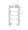
- FIG. 1 is a cross-sectional view schematically showing an example of the configuration of a lighting device 1 according to the first embodiment.
- the lighting device 1 is a device that emits the first light L1 into the lighting space S1.
- the illumination device 1 is arranged, for example, on the ceiling of the illumination space S1.
- the illumination device 1 includes a first light source 2, a first lens optical system 3, a housing 4, and a first shielding section 6.
- the first light source 2 has a first emission portion (e.g. emission surface) 21 that emits the first light L1 into the internal space of the housing 4 .
- the first light L1 is, for example, visible light.
- the first light source 2 may include, for example, a semiconductor laser element such as a laser diode (LD), a light emitting diode element, a vertical cavity surface emitting laser (VCSEL), or a light emitting element such as a super luminescent diode (SLD).
- the first emission part 21 of the first light source 2 may be the emission end of the light emitting element.
- the first light source 2 may further include a light guide member such as a fiber and a rod lens in addition to the light emitting element.
- a fiber includes a linear core and cladding.
- the cladding has a lower refractive index than the core and covers the core.
- the first light L1 can be transmitted through the core while being totally reflected at the interface between the core and the clad.
- a rod lens has, for example, a columnar shape. The first light L1 can pass through the inside of the rod lens while being totally reflected by the side surface of the rod lens.
- the incident end of such a light guide member corresponds to the first end surface located at the longitudinal end of the fiber or the first end surface located at the longitudinal end of the rod lens, and the output end of the light guide member corresponds to the fiber. or the second end surface of the rod lens on the side opposite to the first end surface.
- the first light L1 from the light emitting element is incident on the incident end of the light guide member, travels through the light guide member, and is emitted from the output end of the light guide member into the internal space of the housing 4 .
- the first emitting portion 21 of the first light source 2 corresponds to the emitting end of the light guide member.
- the first emission section 21 may include the wavelength conversion member 23 , and the first light L ⁇ b>1 may be fluorescence emitted from the wavelength conversion member 23 .
- the wavelength conversion member 23 is a wavelength conversion material that converts excitation light into blue light, such as BaMgAl 10 O 17 :Eu or (Sr, Ca, Ba) 10 (PO 4 ) 6 Cl 2 :Eu, ( Sr, Ba) 10 (PO 4 ) 6 Cl 2 :Eu and the like may be included.
- the wavelength conversion member 23 uses, for example, (Sr, Ba, Ca) 5 (PO 4 ) 3 Cl:Eu, Sr 4 Al 14 O 25 :Eu as a wavelength conversion material that converts excitation light into bluish-green light. may contain.
- the wavelength conversion member is a wavelength conversion material that converts excitation light into green light, such as SrSi 2 (O, Cl) 2 N 2 :Eu, (Sr, Ba, Mg) 2 SiO 4 :Eu 2+ , or ZnS : Cu, Al, Zn2SiO4 :Mn, etc. may be included.
- the wavelength conversion member is a wavelength conversion material that converts excitation light into red light, such as Y2O2S :Eu, Y2O3:Eu, SrCaClAlSiN3 : Eu2 + , CaAlSiN3 :Eu, or CaAlSi (ON) 3 : May contain Eu and the like.
- the wavelength conversion member may contain 3Ga 5 O 12 :Cr or the like as a wavelength conversion material that converts excitation light into light having a wavelength in the near-infrared region.
- the first light source 2 in this case is excitation light.
- the excitation light may be, for example, violet light with a peak near 405 nm or blue light with a peak near 450 nm.
- the excitation light is light having a peak in the range from 380 nm to 415 nm and the wavelength conversion member 23 contains RGB phosphors, the color rendering of the illumination device 1 can be enhanced.
- the first light L1 from the first emitting portion 21 of the first light source 2 travels while spreading.
- the size of the first light L1 in the cross section perpendicular to the optical axis AX1 of the first light source 2 increases as the distance from the first light source 2 increases.
- the magnitude of the first light L1 may be defined by a contour line having a light intensity of half the peak value e in the light intensity distribution of the first light L1 in a cross section perpendicular to the optical axis AX1.
- e is called the Napier number.
- the light rays having a light amount of e 1/2 of the peak value of the light amount distribution in the cross section perpendicular to the optical axis AX1.
- the light in the area outside the area enclosed by the contour lines may be regarded as noise.
- the first shielding part 6 is positioned on the path of the first light L1 inside the housing 4, and in the example of FIG. there is As a more specific example, the first shielding portion 6 is positioned immediately after the first emitting portion 21 .
- the first shielding part 6 has, for example, a plate-like shape, and an opening 6a (corresponding to the second opening) is formed in the central part thereof. The opening 6a penetrates the first shielding portion 6 in the optical axis direction along the optical axis AX1.
- first light L1 emitted from the first emitting portion 21 light rays having a relatively small spread angle go straight through the opening 6 a of the first shielding portion 6 and enter the first lens optical system 3 .
- the opening surface 61 forming the opening 6a of the first shielding portion 6 is inclined so as to move away from the optical axis AX1 of the first light L1 toward the front in the traveling direction of the first light L1.
- the aperture surface 61 is inclined away from the optical axis AX1 toward the first lens optical system 3 along the path of the first light L1.
- the aperture surface 61 may have, for example, the same shape as the side surface of a frustum whose height is in the optical axis direction, or may have a curved surface.
- a truncated cone for example, a truncated cone can be adopted.
- the aperture surface 61 is linear in the cross section including the optical axis AX1, and the angle formed by the aperture surface 61 with the optical axis AX1 in the cross section is, for example, about 45 degrees.
- the opening surface 61 may be a reflective surface. That is, the aperture surface 61 may have a high reflectance with respect to the first light L1.
- a highly reflective metal surface may be employed for the aperture surface 61 .
- Such an opening surface 61 may be formed of, for example, mirror-finished metal.
- the reflectance of the aperture surface 61 for the first light L1 may be, for example, 60% or more, 80% or more, or 90% or more.
- the aperture surface 61 may have a high reflectance for the entire wavelength range of the first light L1, or may have a high reflectance for the peak wavelength.
- the reflectance of the aperture surface 61 is, for example, higher than the reflectance of the inner wall of the housing 4 for the first light L1.
- the aperture surface 61 is a reflecting surface, it is possible to reflect the rays of the first light L1 emitted from the first emitting portion 21 with a large divergence angle toward the first lens optical system 3 .
- the inclination angle of the aperture surface 61 is set to an angle that can reflect the first light L ⁇ b>1 from the first emission section 21 toward the first lens optical system 3 . According to this, the amount of the first light L1 incident on the first lens optical system 3 can be improved.
- the opening surface 61 may be a light absorbing surface. In this case, compared with the case where the aperture surface 61 is a reflective surface, scattering inside can be reduced, so a comfortable lighting space with less glare can be realized.
- the spread angle ⁇ 1 of the first light L1 that has passed through the opening 6a of the first shielding portion 6 is smaller than the spread angle ⁇ 0 of the first light L1 at the first emission portion 21 .
- the opening 6a of the first shielding portion 6 is arranged so that the spread angle ⁇ 1 of the first light L1 passing through the opening 6a is smaller than the spread angle ⁇ 0 of the first light L1 at the first emitting portion 21.
- the size, the thickness of the first shielding part 6 and the position of the first shielding part 6 are designed.
- the divergence angle ⁇ 1 referred to here is the angle formed by the outer rays of the first light L1 passing through the opening 6a at the first emission portion 21, for example, in a cross section including the optical axis AX1.
- the spread angle ⁇ 0 (see also FIG. 2) of the first light L1 at the first emission portion 21 is, for example, about 180 degrees.
- the first shielding part 6 is designed so that the spread angle ⁇ 1 of the first light L1 that has passed through the opening 6a is smaller than 180 degrees (for example, about 90 degrees).
- the first shielding part 6 is attached to the inner wall of the first member 42 of the housing 4.
- the first shielding part 6 may be made of the same material as the housing 4 and may be integrally formed.
- the first shielding part 6 may be made of another material and fixed to the housing 4 by a predetermined fixing member.
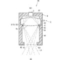
- the first lens optical system 3 is positioned on the path of the first light L1 from the first light source 2 in the internal space of the housing 4.
- the first lens optical system 3 includes a first lens 31 and converges the first light L1 from the first light source 2 onto a virtual image plane IS1 on the side opposite to the first emission section 21 .
- the first lens optical system 3 is an imaging optical system that forms the light source image of the first light source 2 as a real image on the image plane IS1.
- the first emitting portion 21 has a conjugate relationship with the image plane IS1. It should be noted that the conjugate relationship here does not have a strict meaning. ) can be regarded as the image plane IS1.
- the first lens optical system 3 may be composed of a single first lens 31, as illustrated in FIG.
- the first lens 31 may be a spherical biconvex lens.
- the first lens 31 is made of, for example, a material containing at least one of glass such as optical glass and resin such as acrylic resin.
- the first emission section 21 of the first light source 2 is attached to the housing 4 and emits the first light L1 toward the first lens optical system 3 .
- the first light L 1 passes through an irradiation aperture 4 a (corresponding to a first aperture) formed in the housing 4 and exits into the illumination space S 1 outside the housing 4 .
- the irradiation opening 4a is an opening that connects the internal space of the housing 4 and the external illumination space S1.
- the housing 4 has a side wall 41, a first member 42 and a second member 43.
- the side wall 41 has a tubular shape (for example, a cylindrical shape).
- the central axis of the cylindrical side wall 41 and the optical axis AX1 of the first light source 2 substantially match.
- a first member 42 is positioned at the first peripheral edge of the side wall 41 .
- the first member 42 has, for example, a plate-like shape, and the peripheral edge of the first member 42 is connected to the first peripheral edge of the side wall 41 .
- a second member 43 is positioned at a second peripheral edge of the side wall 41 opposite to the first peripheral edge.
- the second member 43 has, for example, a plate-like shape, and the peripheral edge of the second member 43 is connected to the second peripheral edge of the side wall 41 .
- An internal space of the housing 4 is defined by the side wall 41 , the first member 42 and the second member 43 .
- a through-hole is formed in the central portion of the first member 42 so as to pass through the first member 42 in the central axis direction, and the first light source 2 is positioned in the through-hole.
- an irradiation opening 4a is formed in the central portion of the second member 43 so as to penetrate the second member 43 in the central axis direction.
- the second member 43 extends from the lower end of the side wall 41 toward the optical axis AX1 and reaches the periphery of the irradiation aperture 4a. That is, the diameter of the irradiation aperture 4 a is smaller than the inner diameter of the side wall 41 .
- the housing 4 has such a second member 43, the irradiation aperture 4a can be formed small, and the first lens optical system 3 can be made difficult to see from the outside of the housing 4, so that a comfortable image with little glare can be obtained. A lighting space can be realized.
- the first lens optical system 3 is positioned inside the housing 4 between the first emission section 21 of the first light source 2 and the irradiation opening 4 a of the housing 4 .
- the first lens optical system 3 converges the first light L1 from the first light source 2 onto the image plane IS1.
- the image plane IS1 is located within the illumination aperture 4a. That is, the position of the first light source 2, the position of the first lens optical system 3, and the optical conditions of the first lens optical system 3 are designed so that the image plane IS1 is positioned within the irradiation aperture 4a.
- the portion where the first light L1 is most condensed is located in the opening 4a, so when the housing 4 has the second member 43, the opening 4a can be designed to be small. This makes it difficult to see the first lens optical system 3 from the outside of the housing 4 . As a result, a comfortable lighting space with less glare can be achieved.
- the image plane IS1 does not necessarily have to be positioned inside the irradiation aperture 4a.
- the image plane IS1 may be positioned slightly displaced from the irradiation aperture 4a in the traveling direction of the first light L1 passing through the irradiation aperture 4a. That is, the image plane IS1 may be positioned slightly closer to the inside of the housing 4 than the irradiation aperture 4a, or may be positioned slightly closer to the illumination space S1.
- the size M1 of the first light L1 at the first emitting portion 21 can be said to be the size of the first emitting portion 21 itself, and corresponds to, for example, the area of the end surface of the core of the fiber or the area of the end surface of the rod lens.
- the size of the end surface of the light emitting element itself corresponds to the size M1 of the first light L1 at the first emitting portion 21 .
- the size of the surface of the wavelength converting member 23 corresponds to the size M1 of the first light L1 at the first emitting portion 21 .
- the first light source 2 is, for example, an LD
- the light emission diameter can be made smaller than that of an LED or VCSEL, and the size M2 of the first light L1 on the image plane IS1 can be made relatively small. . As a result, a comfortable lighting space with less glare can be achieved.
- the size M1 may be regarded as the diameter of the first light L1.
- the size M1 of the first light L1 at the first emitting portion 21 is, for example, about 2 mm to 3 mm.
- the size M3 of the irradiation aperture 4a refers to the area of the irradiation aperture 4a in the cross section perpendicular to the optical axis AX1 in the irradiation aperture 4a.
- the diameter or diagonal length of the irradiation aperture 4a is, for example, several millimeters to several tens of millimeters.
- the diameter of the irradiation aperture 4a may be, for example, about 5 mm to 15 mm.
- the size M3 of the irradiation aperture 4a differs at each position on the optical axis AX1.
- the minimum value can be adopted as the size M3 of the irradiation aperture 4a.
- the imaging magnification is the ratio of the magnitude M2 of the first light L1 on the image plane IS1 to the magnitude M1 of the first light L1 at the first emission portion 21 of the first light source 2 .
- the size M2 of the first light L1 on the image plane IS1 can be made equal to or less than the size M3 of the irradiation aperture 4a. Therefore, the possibility of the first light L1 entering the second member 43 can be reduced, and the possibility of the first light L1 being reflected or scattered by the inner surface of the cylindrical side wall 41 or the second member 43 can be reduced. can be reduced. As a result, it is possible to reduce unnecessary reflected and scattered light leaking from the irradiation aperture 4a.
- the imaging magnification of the first lens optical system 3 may be set so that the size of the first light L1 passing through the irradiation aperture 4a is smaller than that of the irradiation aperture 4a. According to this, the reflected scattered light can be further reduced.
- the spread angle ⁇ 1 is less than or equal to the angle ⁇ 2 that defines the numerical aperture of the first lens optical system 3 .
- the numerical aperture is the product of the half sine of the angle ⁇ 2 and the refractive index.
- FIG. 2 is a diagram for explaining the angle ⁇ 2 that defines the numerical aperture of the first lens optical system 3. As shown in FIG.
- the angle ⁇ 2 here is, for example, the angle formed by the outer rays of virtual light passing through the effective area of the first lens optical system 3 .
- the effective area referred to here corresponds to a light passage area in which the optical performance of the first lens optical system 3 can be exhibited.
- the effective area of the first lens 31 is a predetermined This is the area excluding the peripheral edge width.
- the effective area of the first lens 31 may be an area surrounded by the inner peripheral edge of the portion of the housing 4 that holds the peripheral edge of the first lens 31 (that is, the lens holder).
- the light rays on both sides of the first light L1 may be light rays that define the emission diameter of the first light L1, for example.
- the light rays on both sides of the first light L1 may be light rays that define the size of the first light L1 in a cross section perpendicular to the optical axis AX1 of the first light source 2 .
- the divergence angle ⁇ 1 is equal to or less than the angle ⁇ 2
- the first light L1 that has passed through the opening 6a of the first shielding portion 6 can pass through the effective area of the first lens optical system 3. Therefore, the first light L1 hardly enters the edge of the first lens 31, and unnecessary reflection and scattering of the first light L1 occurring at the edge can be suppressed or avoided.
- the angle ⁇ 2 that defines the numerical aperture of the first lens optical system 3 is larger than the spread angle ⁇ 1 of the first light L1 that has passed through the opening 6a of the first shielding portion 6, and is ( It may be smaller than the spread angle ⁇ 0 of the first light L1 (before passing through the opening 6a of the first shielding portion 6).
- the imaging magnification of the first lens optical system 3 is equal to or less than the above ratio, and the spread angle ⁇ 1 is equal to or less than the angle ⁇ 2. Therefore, unnecessary reflection and scattering of the first light L1 at the periphery of the first lens optical system 3 and the irradiation aperture 4a can be suppressed or avoided. Therefore, it is possible to reduce the reflected scattered light that leaks into the illumination space S1, so that it is possible to suppress unevenness such as glare in the first light L1 emitted to the illumination space S1. Therefore, the illumination device 1 can irradiate the illumination space S1 with the high-quality first light L1.
- the first light L1 may be emitted from the irradiation opening 4a so as not to contact the housing 4.
- “not in contact” does not have a strict meaning. Noise such as noise may be in contact with the housing 4 .
- FIG. 3 is a cross-sectional view schematically showing a first aspect of the configuration of the lighting device 1.
- the image plane IS1 is curved.
- the image plane IS1 is curved so as to be convex toward the illumination space S1.
- Such a first lens optical system 3 can be configured with an inexpensive first lens 31 . Therefore, the manufacturing cost of the lighting device 1 can be reduced.
- the first lens 31 may have a continuous curved surface.
- the main surface of the first lens 31 through which the first light L1 passes may be composed only of a curved surface without steps.
- the first lens 31 may not be a Fresnel lens. Thereby, scattering or reflection at the first lens 31 can be reduced. As a result, a comfortable lighting space with less glare can be achieved.
- FIG. 4 is a cross-sectional view schematically showing a second aspect of the configuration of the lighting device 1.
- the first lens optical system 3 includes multiple first lenses 31 .
- the multiple first lenses 31 are arranged side by side on the path of the first light L1.
- the plurality of first lenses 31 may be arranged side by side in the optical axis direction of the first light L1.
- Such a plurality of first lenses 31 can also be called a group lens.
- optical characteristics necessary for the first lens optical system 3 can be easily obtained even if a special optical element such as a Fresnel lens is not used.
- FIG. 5 is a cross-sectional view schematically showing a third aspect of the configuration of the illumination device 1.
- the configuration of the third aspect is the same as that of the second aspect.
- a portion (waist portion LW1) where the light diameter of the first light L1 is smaller than the light diameter passing through each of the plurality of first lenses 31 may have Specifically, the minimum value of the light diameter between two adjacent first lenses 31 (that is, the diameter of the waist portion LW1) is the minimum light diameter of the first light L1 in each of the two first lenses 31. may be less than the value
- the first lens optical system 3 with high imaging magnification can be easily obtained.
- the first lens optical system 3 may have, for example, three or more lenses arranged side by side in the optical axis direction of the first light L1. Thereby, the optical characteristics required for the first lens optical system 3 can be obtained more easily.
- each first lens 31 is a spherical lens in the examples of FIGS. 1 to 5, each first lens 31 may be an aspherical lens or a free-form surface lens.
- the orientation angle of the first light L1 emitted from the irradiation aperture 4a may be less than 60 degrees.
- the orientation angle of the illumination device 1 may be less than 45 degrees, less than 30 degrees or less than 15 degrees, for example.
- FIG. 6 is a cross-sectional view schematically showing a fourth aspect of the configuration of the lighting device 1.
- the opening surface 61 of the first shielding portion 6 is substantially parallel to the optical axis AX1.
- the aperture surface 61 has, for example, the same shape as a columnar side surface whose height direction is the optical axis direction.
- the first shielding part 6 has, for example, a ring shape.
- the aperture surface 61 is for example an absorption surface. That is, the absorption rate of the aperture surface 61 for the first light L1 is high.
- the absorption rate of the opening surface 61 may be, for example, 60% or more, 80% or more, or 90% or more.
- the aperture surface 61 may have a high absorptance for the entire wavelength range of the first light L1, or may have a high absorptance for the peak wavelength.
- the opening surface 61 is formed by performing a blackening process, for example.
- blackening treatment such as chemical conversion treatment, plating, and painting can be employed as the blackening treatment.
- a matte blackening treatment may be employed, or a glossy blackening treatment may be employed.
- Such an opening surface 61 is made of a black material.
- the material includes, for example, at least one of black metal, black metal oxide film, and black resin.
- the opening surface 61 may be formed by a dielectric multilayer film.
- a dielectric multilayer film has, for example, a structure in which a plurality of dielectric thin films are laminated.
- Dielectrics include, for example, one or more of titanium oxide (TiO 2 ), SiO 2 , niobium pentoxide (Nb 2 O 5 ), tantalum pentoxide (Ta 2 O 5 ), and magnesium fluoride (MgF 2 ). of materials are used.
- Such a dielectric multilayer film can also be called a low reflection film or an antireflection film.
- the spread angle ⁇ 1 of the first light L1 that has passed through the opening 6a of the first shielding portion 6 is smaller than the spread angle of the first light L1 in the first emission portion 21 .
- the divergence angle ⁇ 1 is equal to or less than the angle ⁇ 2 that defines the numerical aperture of the first lens optical system 3. Therefore, the first light L ⁇ b>1 that has passed through the opening 6 a of the first shielding portion 6 can pass through the effective area of the first lens optical system 3 . Therefore, it is possible to suppress reflected and scattered light inside the housing 4 and suppress unevenness of the first light L1 emitted from the irradiation opening 4a.
- FIG. 7 is a cross-sectional view schematically showing part of the fifth aspect of the configuration of the lighting device 1.
- the first member 42 of the housing 4 is formed with an opening for passing the light from the first emitting portion 21 .
- the opening of the first member 42 functions as the opening 6 a of the first shielding portion 6 . That is, the first shielding portion 6 is configured integrally with the first member 42 .
- the housing 4 further includes a transparent connecting member 44 that connects the first light source 2 to the first member 42 .
- the connecting member 44 has an annular shape surrounding the optical axis AX1, the outer peripheral edge of the lower surface of the connecting member 44 is connected to the upper surface of the first member 42, and the inner peripheral portion of the connecting member 44 is the first light source. 2.
- the inner peripheral edge portion of the lower surface of the connecting member 44 faces the opening 6 a of the first shielding portion 6 .
- the connecting member 44 has a high transmittance for the first light L1.
- the transmittance is, for example, 60% or higher, and may be 70% or higher, 80% or higher, or 90% or higher.
- a portion of the light emitted from the first emitting portion 21 of the first light source 2 passes through the opening 6a of the first shielding portion 6, and the rest of the light is reflected or scattered by the opening surface 61 of the first shielding portion 6.
- the opening surface 61 forming the opening 6a of the first shielding portion 6 is inclined so as to approach the optical axis AX1 of the first light L1 toward the front in the traveling direction of the first light L1. ing.
- scattering of light generated at the opening surface 61 is directed toward the first emitting portion 21 side, so scattered light can be made less likely to occur inside the housing 4 .
- the scattered light travels through the transparent connecting member 44 to the outside of the housing 4 .
- the inclination angle of the opening surface 61 is set to a value that causes the scattered light to be directed toward the connecting member 44 around the first emitting portion 21 . Therefore, as compared with the case where the aperture surface 61 is inclined away from the optical axis AX1, scattering inside can be reduced, and a comfortable lighting space with little glare can be realized.
- the first emitting portion 21 and the first shielding portion 6 may be separated in the direction perpendicular to the optical axis AX1. That is, the opening surface 61 forming the opening 6a of the first shielding portion 6 may be separated from the first emitting portion 21 in the direction perpendicular to the optical axis AX1.
- the size M1 of the first emitting portion 21 may be smaller than the size M4 of the opening 6a of the first shielding portion 6 (that is, the opening area).
- the width of the first emitting portion 21 may be smaller than the width of the opening 6 a of the first shielding portion 6 .
- the width of the output end of the first output portion 21 and the width of the opening 6a of the first shielding portion 6 may match.
- the first emitting portion 21 and the first shielding portion 6 can further reduce glare compared to a structure in which the first emitting portion 21 and the first shielding portion 6 are separated in the direction perpendicular to the optical axis AX1.
- matching here means that an error is allowed. That is, the meaning of coincidence also includes the situation where A and B deviate within tolerance.
- the first emitting portion 21 and the first shielding portion 6 may partially overlap in the direction perpendicular to the optical axis AX1.
- the width of the opening 6 a of the first shielding portion 6 (that is, the diameter of the through hole of the first member 42 ) may be smaller than the width of the emission end of the first emission portion 21 .
- the width of the output end of the first output portion 21 and the width of the opening 6a of the first shielding portion 6 are substantially the same. In comparison, glare can be further reduced.
- the first emitting portion 21 and the first shielding portion 6 may be continuous in the optical axis direction, or may partially overlap each other. However, as shown in FIG. 9, the first emitting portion 21 and the first shielding portion 6 may be separated in the optical axis direction.
- the housing 4 may further include a transparent connecting member 44 , and the transparent connecting member 44 may connect the first light source 2 to the first member 42 .
- the aperture surface 61 of the first shielding portion 6 may be inclined along the path of the first light L1 so as to move away from the optical axis AX1 toward the first lens optical system 3.
- a ray with a large spread angle among the first light L1 may enter the upper end portion of the aperture surface 61 .
- the upper end portion referred to here is, for example, a connecting portion between the opening surface 61 of the first shielding portion 6 and the surface 62 on the first light source 2 side.
- the light rays of the first light L1 having a large spread angle may be incident on the surface 62 of the first shielding portion 6 on the side of the first light source 2 .
- surface 62 may be a light absorbing surface.
- the light absorbing surface may be, for example, a surface having an absorptance of 60% or more in the visible light region.
- the first light L1 from the first emitting portion 21 does not have to enter the opening surface 61 of the first shielding portion 6 directly.
- the aperture surface 61 may be more inclined with respect to the optical axis AX1 than the outermost rays of the first light L1 that have passed through the aperture surface 61 .
- the acute angle formed by the aperture surface 61 and the optical axis AX1 may be larger than the acute angle formed by the light ray and the optical axis AX1.
- the aperture surface 61 may be inclined so that the acute angle formed by the aperture surface 61 and the optical axis AX1 becomes smaller. According to this, the first light L ⁇ b>1 from the first emitting portion 21 can directly enter the aperture surface 61 .
- at least one of the aperture surface 61 and the surface 62 may be a light absorbing surface.
- the distance between the first emission section 21 and the irradiation opening 4a is larger than the inner diameter of the housing 4.
- the distance between the first emission section 21 and the irradiation aperture 4a referred to here is, for example, the distance along the path along the optical axis AX1.
- the distance between the first lens optical system 3 and the irradiation aperture 4a can be increased.
- the first lens optical system 3 includes a plurality of first lenses 31, the distance between the first lens 31 closest to the irradiation aperture 4a and the irradiation aperture 4a can be increased.
- the first lens optical system 3 can be made difficult to see from the outside of the housing 4, and a comfortable lighting space with less glare can be realized.
- the distance between the first lens optical system 3 and the irradiation aperture 4 a may be larger than the inner diameter of the housing 4 .
- FIG. 11 is a cross-sectional view showing an example of the configuration of a lighting device 1A according to the second embodiment.
- the illumination device 1A differs from the illumination device 1 in the position of the first shielding portion 6.
- the first shielding portion 6 is positioned after the frontmost first lens 31 in the first lens optical system 3.
- the aperture position of the first lens optical system 3 located in the vicinity of The aperture position referred to here means that, for example, when a plane A1 perpendicular to the optical axis AX1 is moved along the optical axis direction, each first light L1 emitted from each point of the first emission section 21 is a plane.
- the first light L1 emitted from each of the three points on the first emission section 21 is called a first partial light L1a, a first partial light L1b, and a first partial light L1c.
- the first partial light L1a, the first partial light L1b, and the first partial light L1c overlap each other on the plane A1 at the stop position. That is, on the plane A1 shown in FIG. 11, the proportion of the area where the first partial lights L1a to L1c overlap with respect to the entire area of the first light L1 is the highest.
- the first lens optical system 3 includes a single first lens 31, and the aperture position of the first lens optical system 3 is located immediately after the first lens 31. Therefore, the first shielding part 6 is provided immediately after the first lens 31 .
- the central portion of the first light L1 transmitted through the first lens 31 passes through the opening 6a of the first shielding portion 6, and the remaining outer peripheral portion is shielded by the first shielding portion 6.
- FIG. The first light L1 that has passed through the opening 6a of the first shielding portion 6 forms an image on the image plane IS1, passes through the irradiation opening 4a, and exits into the illumination space S1, as in the first embodiment.
- the divergence angle ⁇ 1 is equal to or less than the angle ⁇ 2 that defines the numerical aperture of the first lens optical system 3.
- the divergence angle ⁇ 1 is the angle formed by the outer rays of the first light L1 passing through the opening 6a of the first shielding portion 6 at the first emitting portion 21 in the cross section including the optical axis AX1.
- the first shielding part 6 can allow the first light L1 passing through the effective area of the first lens optical system 3 to pass through the opening 6a. Therefore, the lighting device 1A can also emit the first light L1 with less unevenness from the irradiation opening 4a.
- the first shielding part 6 is positioned near the diaphragm position. According to this, a ray passing through the center of the first partial lights L1a to L1c emitted from each point of the first emitting portion 21 passes through the center of the opening 6a of the first shielding portion 6. FIG. Therefore, the first partial lights L1a to L1c emitted from each point are more evenly shielded by the first shielding portion 6.
- FIG. 1 a ray passing through the center of the first partial lights L1a to L1c emitted from each point of the first emitting portion 21 passes through the center of the opening 6a of the first shielding portion 6.
- the illumination device 1A can maintain the in-plane distribution of the intensity of the first light L1 in the first emission section 21 and emit the first light L1 from the irradiation aperture 4a. That is, the illumination device 1A can emit the first light L1 into the illumination space S1 with the in-plane distribution that reflects the in-plane distribution of the first light L1 in the first emission section 21 as it is. For example, if the in-plane distribution of the first light L1 in the first emission section 21 is uniform, the illumination device 1A can emit the first light L1 into the illumination space S1 with the uniform in-plane distribution.
- the first shielding part 6 should be positioned at the stop position.
- the first shielding portion 6 does not necessarily have to be positioned at the stop position.
- the first shielding portion 6 may be located closer to the irradiation opening 4a than the stop position. This also allows the first light L1 that has passed through the effective area of the first lens optical system 3 to be emitted from the irradiation aperture 4a.
- the first shielding part 6 is the final first lens in the first lens optical system 3 . It is preferable that it is located closer to the first light source 2 than the lens 31 is. According to this, even if the first light L ⁇ b>1 is reflected and scattered by the aperture surface 61 of the first shielding section 6 , the reflected scattered light enters the first lens 31 in the rear stage of the first shielding section 6 . According to this, compared with the case where the first lens 31 is not positioned after the first shielding part 6, the reflected scattered light emitted from the irradiation aperture 4a can be reduced.
- first and second embodiments although the single first shielding part 6 is positioned inside the housing 4, two first shielding parts 6 may be positioned. Specifically, one first shielding portion 6 (see FIG. 1) is located between the first output portion 21 and the first lens optical system 3, and the other first shielding portion 6 (see FIG. 11) is For example, it may be positioned at the diaphragm position of the first lens optical system 3 .
- part of the first light L1 can be reflected and scattered by the first shielding section 6 . If such reflected scattered light deviates from the path of the first light L1 that forms an image on the image plane IS1 and leaks out of the irradiation aperture 4a without forming an image on the image plane IS1, the first light L1 becomes uneven. can occur.
- the reflected scattered light of the first light L1 reflected and scattered inside the housing 4 is also referred to as the reflected scattered light L11.
- the reflected scattered light L11 is a part of the first light L1 that deviates from the path of the first light L1 that forms an image on the image plane IS1, and may be either reflected light or scattered light.
- the third embodiment it is intended to further suppress unevenness of the first light L1 that illuminates the illumination space S1.
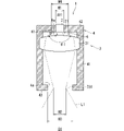
- FIG. 12 is a cross-sectional view schematically showing an example of the configuration of a lighting device 1B according to the third embodiment.
- the illumination device 1B differs from the illumination device 1 in the presence or absence of the light reducing structure 5.
- FIG. The light reducing structure 5 is located inside the housing 4 .
- the light reduction structure 5 is arranged to reduce the reflected scattered light L11 emerging from the illumination aperture 4a.
- the first lens optical system 3 of the illumination device 1B includes multiple first lenses 31 and one or more spacers 32 .
- the first lens optical system 3 includes two first lenses 31 and one spacer 32 .
- the spacer 32 is a member that defines the interval between the two first lenses 31 .
- the spacer 32 is positioned between two adjacent first lenses 31 and contacts both first lenses 31 . Thereby, the distance between the two first lenses 31 can be matched with the thickness of the spacer 32 (thickness along the optical axis AX1).
- the spacer 32 has, for example, a ring shape surrounding the optical axis AX1.
- the light reducing structure 5 is positioned on the inner wall of the spacer 32 and exposed to the inner space of the housing 4.
- the light reducing structure 5 includes, for example, a reflection reducing portion 51 .
- the reflection reduction section 51 may include an absorption film having a high absorption rate for the first light L1.
- the absorption rate may be, for example, 60% or more, 80% or more, or 90% or more.
- the reflection reducing portion 51 may have a high absorptance for the entire wavelength range of the first light L1, or may have a high absorptance for the peak wavelength.
- the absorption rate of the reflection reducing portion 51 for the first light L1 is higher than the absorption rate of the spacer 32 for the first light L1.
- Such a reflection reducing portion 51 is formed, for example, by blackening the inner wall of the spacer 32 .
- the reflection reducing portion 51 is formed on the inner wall of the spacer 32 by chemical conversion treatment, plating, and blackening treatment such as painting.
- the blackening treatment a matte blackening treatment may be employed, or a glossy blackening treatment may be employed.
- Such a reflection reducing portion 51 is made of a black material.
- the material includes, for example, at least one of black metal, black metal oxide film, and black resin.
- the reflection reducing portion 51 may include a dielectric multilayer film.
- a dielectric multilayer film has, for example, a structure in which a plurality of dielectric thin films are laminated.
- Dielectrics include, for example, one or more of titanium oxide (TiO 2 ), SiO 2 , niobium pentoxide (Nb 2 O 5 ), tantalum pentoxide (Ta 2 O 5 ), and magnesium fluoride (MgF 2 ). of materials are used.
- Such a dielectric multilayer film can also be called a low reflection film or an antireflection film.
- the reflection reducing portion 51 may be formed directly on the inner wall of the spacer 32 or may be formed on a predetermined film-like base material and the base material may be attached to the inner wall of the spacer 32 .
- the substrate may be attached to the inner wall of the spacer 32, for example by an adhesive.
- the reflection reduction section 51 may contain flocked paper.
- flocked paper can consist of a substrate such as paper and cloth, and chemical fibers attached to the substrate in an upright position. If black flocked paper is used, it is possible to further suppress reflection of the reflected scattered light L11 compared to other colors of flocked paper.
- the illumination device 1B can emit the first light L1 of higher quality into the illumination space S1.
- FIG. 13 is an enlarged view schematically showing part of another example of the light reducing structure 5.
- FIG. The light reducing structure 5 includes uneven features 52 .
- the uneven shape 52 is, for example, the shape of the inner wall surface of the spacer 32, and a part thereof is schematically shown in FIG.
- the uneven shape 52 presents unevenness in the optical axis direction parallel to the optical axis AX1. That is, the uneven shape 52 has a shape in which concave portions and convex portions are alternately arranged in a cross section including the optical axis AX1.
- the concave-convex shape 52 has a saw blade shape, and each tooth (that is, convex portion) of the saw blade is formed on the first surface 521 on the side of the first light source 2 and the first surface 521 on the side of the irradiation aperture 4a. 2 faces 522 .
- the first surface 521 is inclined in the optical axis direction so as to approach the optical axis AX1 toward the irradiation aperture 4a
- the second surface 522 is inclined away from the optical axis AX1 toward the irradiation aperture 4a. Tilt away.
- the first surfaces 521 and the second surfaces 522 are alternately continuous. As illustrated in FIG.
- the length of the first surface 521 and the length of the second surface 522 may be approximately the same.
- the first surface 521 and the second surface 522 may be equal sides of an isosceles triangle in a cross section (for example, the paper surface of FIG. 13) including the optical axis AX1.
- Such uneven shape 52 may have a helical shape similar to a female thread, or may have a shape in which a plurality of ring shapes are arranged in the optical axis direction.
- the pitch of the concave-convex shape 52 is set to, for example, several millimeters or less.
- the reflected scattered light L11 is obliquely incident on the inner wall of the spacer 32 mainly from the first light source 2 side. Therefore, more reflected scattered light L11 is incident on the first surface 521 than on the second surface 522 on the inner wall of the spacer 32 .
- the first surface 521 reflects and scatters the incident reflected scattered light L11 mainly in an oblique direction opposite to the irradiation aperture 4a.
- the number of times the reflected scattered light L11 is reflected and scattered within the housing 4 can be increased, and the reflected scattered light L11 can be attenuated within the housing 4 . Therefore, it is possible to reduce the possibility that the reflected scattered light L11 is emitted from the irradiation aperture 4a.
- the reflected scattered light L11 even if the reflected scattered light L11 enters the second surface 522 from the first light source 2 side, the reflected scattered light L11 reflected and scattered by the second surface 522 mainly enters the first surface 521, and the first surface 521 are reflected and scattered obliquely toward the first light source 2 side. Therefore, it is possible to reduce the possibility that the reflected scattered light L11 is emitted from the irradiation aperture 4a.
- the illumination device 1B can emit the first light L1 of higher quality into the illumination space S1.
- FIG. 14 is a diagram schematically showing another example of the uneven shape 52. As shown in FIG. In the example of FIG. 14 as well, the uneven shape 52 is the shape of the inner wall surface of the spacer 32 . However, in the example of FIG. 14, the length of the second surface 522, which is further away from the optical axis AX1 toward the irradiation aperture 4a, is longer than the length of the first surface 521. As shown in FIG. In the example of FIG.
- the first surface 521 is substantially perpendicular to the optical axis AX1, so in the cross section including the optical axis AX1, the first surface 521 corresponds to the adjacent side of a right triangle and is perpendicular to the second surface 522. Corresponds to the hypotenuse of a triangle.
- the reflected scattered light L11 is also incident on the inner wall surface of the spacer 32 as described above, mainly from the side of the first light source 2 in an oblique direction.
- the first surface 521 reflects and scatters the incident reflected scattered light L11 mainly toward the side opposite to the irradiation aperture 4a.
- the first surface 521 mainly reflects and scatters the reflected scattered light L11 obliquely toward the first light source 2 side.
- part of the reflected and scattered light L11 from the first surface 521 may enter the second surface 522, since the second surface 522 is inclined, most of the reflected and scattered light L11 is directed obliquely toward the first light source 2 side. Can be reflected and scattered in directions.
- the reflected scattered light L11 from the first light source 2 side enters the second surface 522
- the reflected scattered light L11 reflected and scattered by the second surface 522 enters the first surface 521
- the first surface 521 is reflected and scattered obliquely to the first light source 2 side.
- the reflected scattered light L11 incident on the uneven shape 52 from the first light source 2 side can be mainly reflected and scattered in the oblique direction toward the first light source 2 side. Therefore, it is possible to reduce the possibility that the reflected scattered light L11 is emitted from the irradiation aperture 4a.
- FIG. 15 is a cross-sectional view schematically showing a first aspect of lighting device 1B.
- the light reducing structure 5 is located on the inner wall of the housing 4 .
- the light reducing structure 5 may include a reflection reducing portion 51 . According to this, reflection of the reflected scattered light L11 incident on the reflection reducing portion 51 is suppressed, so that the reflected scattered light L11 emitted from the irradiation aperture 4a into the illumination space S1 can be reduced.
- the reflection reducing section 51 may be located on almost the entire inner wall of the housing 4 as illustrated in FIG. 15, or may be located only on a part thereof.
- the reflection reducing portion 51 may be located on all or part of the inner wall of the side wall 41 surrounding the optical axis AX1.
- the reflection reducing portion 51 is positioned along the entire circumference of the inner wall of the side wall 41 .
- the reflection reducing portion 51 may be positioned on the surface of the first shielding portion 6 on the side of the first lens optical system 3 .
- FIG. 16 is a cross-sectional view schematically showing a second aspect of the lighting device 1B.
- the light reducing structure 5 located on the inner wall of the housing 4 may have an uneven shape 52 . That is, the inner wall of the housing 4 may have the uneven shape 52 as the light reducing structure 5 .
- the uneven shape 52 may be formed on the entire inner wall surface of the housing 4, or may be formed only on a part thereof.
- the uneven shape 52 can be formed at least on all or part of the inner wall surface of the side wall 41 .
- the uneven shape 52 is formed along the entire circumference of the inner wall surface of the side wall 41 .
- the reflected and scattered light L11 that obliquely enters the uneven shape 52 of the inner wall of the side wall 41 from the first light source 2 side is mainly reflected and scattered obliquely toward the first light source 2 side. Therefore, the reflected scattered light L11 emitted from the irradiation aperture 4a to the illumination space S1 can be reduced.
- FIG. 17 is a cross-sectional view schematically showing a third aspect of the illumination device 1B according to the third embodiment.
- the illumination device 1B according to the third aspect differs from the illumination device 1A in the presence or absence of the light reducing structure 5.
- the first shielding portion 6 is positioned near the stop position, and the light reducing structure 5 is positioned on the first shielding portion 6 .
- the light reducing structure 5 is positioned on the opening surface 61 forming the opening 6 a of the first shielding portion 6 .
- the light reducing structure 5 may be positioned all around the aperture surface 61 .
- the light reducing structure 5 may include a reflection reducing portion 51 and may have an uneven shape 52 .
- the reflected scattered light L11 incident on the opening surface 61 of the first shielding portion 6 in an oblique direction from the first light source 2 side is suppressed, or the reflected scattered light L11 is mainly emitted from the first light source 2 side. Reflect and scatter diagonally. Therefore, the reflected scattered light L11 emitted from the irradiation aperture 4a to the illumination space S1 can be reduced.
- the light reduction structure 5 may be positioned on the first shielding section 6 while avoiding the surface 63 on the irradiation aperture 4a side of the surface of the first shielding section 6 . This is because the reflected scattered light L11 is less incident on the surface 63 of the first shielding portion 6 than on the opening surface 61 . Further, the light reducing structure 5 may be positioned in the first shielding portion 6 while avoiding the surface 62 of the first shielding portion 6 on the side of the irradiation opening 4a. This is because the reflected scattered light L11 incident on the surface 62 of the first shielding portion 6 is reflected and scattered toward the first light source 2, and thus is difficult to be emitted from the irradiation opening 4a.
- the light reduction structure 5 is positioned on at least one of the inner wall of the spacer 32, the inner wall of the housing 4, and the first shielding portion 6. However, it is not necessarily limited to this. In short, the light reduction structure 5 is exposed in the internal space of the housing 4 and arranged at a position where it does not interfere with the first light L1 passing through the first lens optical system 3 and forming an image on the image plane IS1.
- the light reducing structure 5 may be located on the surface of a lens holder (not shown) that holds the lens 31 .
- the light reduction structure 5 may include both the reflection reduction portion 51 and the uneven shape 52 .
- the reflection reducing portion 51 is positioned on the surface of the uneven shape 52 .
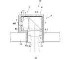
- FIG. 18 is a cross-sectional view schematically showing an example of the configuration of a lighting device 1C according to the fourth embodiment.
- the illumination device 1 ⁇ /b>C differs from the illumination device 1 in the specific configuration of the first lens optical system 3 .
- the first lens optical system 3 includes a plurality of first lenses 31 and constitutes a bilateral telecentric optical system.
- the double-telecentric optical system means that the principal ray of the first light L1 is parallel to the optical axis AX1 on the first light source 2 side, and the principal ray of the first light L1 is parallel to the optical axis AX1 on the irradiation aperture 4a side.
- the chief ray of the first light L1 emitted from each point of the first emission portion 21 is indicated by a thick dashed line.
- a principal ray is a ray that passes through the center of the first light L1 on a plane A1 perpendicular to the optical axis AX1 at the stop position. As illustrated in FIG. 18, among the rays of the first partial light L1a, the principal ray passing through the center of the first light L1 on the plane A1 is located on the optical axis AX1 on both the first light source 2 side and the irradiation aperture 4a side.
- the principal ray of the first partial light L1b is also parallel to the optical axis AX1 on both the first light source 2 side and the irradiation aperture 4a side
- the principal ray of the first partial light L1c is also parallel to the first light source 2 side and the irradiation aperture 4a side. Both sides of 4a are parallel to the optical axis AX1.
- first lenses 31 are schematically shown in the example of FIG. 18, the number of first lenses 31 can be changed as appropriate. Also, in the example of FIG. 18, a double-sided convex lens is shown as the first lens 31, but other lenses such as a concave lens may be employed as appropriate.
- the principal ray of the first light L1 emitted from the irradiation aperture 4a is substantially parallel and hardly spreads. According to this, it is possible to reduce the spread angle of the first light L1 emitted from the irradiation opening 4a. Therefore, a narrower irradiation area can be irradiated with the first light L1, and the presence of the lighting device 1C can be further reduced.
- ⁇ Fifth Embodiment> 19 and 20 are cross-sectional views schematically showing an example of the configuration of a lighting device 1D according to the fifth embodiment.
- the illumination device 1D differs from the illumination device 1 in the presence or absence of a zoom mechanism 35.
- FIG. 19 and 20 are cross-sectional views schematically showing an example of the configuration of a lighting device 1D according to the fifth embodiment.
- the illumination device 1D differs from the illumination device 1 in the presence or absence of a zoom mechanism 35.
- the zoom mechanism 35 zooms, that is, adjusts the spread angle of the first light L1 from the irradiation aperture 4a by adjusting the positions of the first lenses 31 constituting the first lens optical system 3 on the optical axis AX1.
- the zoom mechanism 35 may have, for example, a ball screw mechanism.
- a ball screw mechanism includes a lead screw extending in the direction of the optical axis, a carriage coupled to the lead screw by screw action, a lens holder coupled to the carriage to hold the first lens 31, and a motor for rotating the lead screw. including. By rotating the lead screw, the carriage, the lens holder and the first lens 31 move together along the optical axis direction.
- the motor is controlled by the controller 20, for example.
- Control unit 20 can also be said to be a control circuit.
- Control unit 20 includes at least one processor to provide control and processing power to perform various functions, as described in further detail below.
- the at least one processor may be implemented as a single integrated circuit (IC) or as multiple communicatively coupled integrated circuit ICs and/or discrete circuits. good.
- the at least one processor can be implemented according to various known techniques.
- a processor includes one or more circuits or units configured to perform one or more data computing procedures or processes, such as by executing instructions stored in associated memory.
- the processor may be firmware (eg, discrete logic components) configured to perform one or more data computing procedures or processes.
- the processor is one or more processors, controllers, microprocessors, microcontrollers, application specific integrated circuits (ASICs), digital signal processors, programmable logic devices, field programmable gate arrays, or any of these. Any combination of devices or configurations, or other known combinations of devices and configurations, may be included to perform the functions described below.
- ASICs application specific integrated circuits
- the housing 4 may be composed of a plurality of cylindrical bodies, and may move along the optical axis direction together with each first lens 31 . That is, the zoom mechanism 35 may move the first lens 31 and the cylindrical body integrally. According to this, the size of the housing 4 in the optical axis direction changes according to the position of each first lens 31 .
- the distance D1 between the first emitting portion 21 of the first light source 2 and the first lens 31 and the distance D2 between two adjacent first lenses 31 are wider than in FIG. Thereby, the spread angle of the first light L1 emitted from the irradiation aperture 4a of the illumination device 1D can be reduced.
- the zoom mechanism 35 adjusts the position of each first lens 31, thereby adjusting the spread angle of the first light L1 emitted from the irradiation aperture 4a. Therefore, the size of the irradiation area can be adjusted.
- the angle ⁇ 2 that defines the numerical aperture also changes.
- the spread angle ⁇ 1 may be set to a minimum value or less within the range of the angle ⁇ 2 that can be taken by the movement of the first lens 31, or the spread angle ⁇ 1 may change according to the angle ⁇ 2.
- the first shielding part 6 may include a diaphragm mechanism 64 that changes the size of the opening 6a.
- FIG. 21 is a plan view schematically showing an example of the configuration of the first shielding part 6.
- the diaphragm mechanism 64 includes a plurality of diaphragm blades 641 and a rotating member 642 .
- a plurality of aperture blades 641 are arranged in the circumferential direction around the optical axis AX1, and the tip of each aperture blade 641 forms a part of the aperture surface 61, respectively.
- the rotating member 642 is a member that displaces the aperture blade 641, and has, for example, a ring-shaped plate shape surrounding the optical axis AX1.
- the rotating member 642 is coupled to the diaphragm blades 641 so as to be displaceable, and by rotating around the optical axis AX1, the plurality of diaphragm blades 641 are displaced, and the size of the aperture 6a is changed.
- the diaphragm mechanism 64 includes, for example, a driving section such as a motor (not shown) that rotates the rotating member 642 .
- the diaphragm mechanism 64 is controlled by the controller 20, for example.
- the control unit 20 controls the aperture mechanism 64 according to the position of the first lens 31 so that the divergence angle ⁇ 1 is equal to or less than the angle ⁇ 2. For example, the control unit 20 receives from the outside a signal specifying the spread angle of the first light L1 emitted by the illumination device 1D.
- the controller 20 controls the zoom mechanism 35 and the aperture mechanism 64 based on the signal. Specifically, the control unit 20 controls the zoom mechanism 35 so that the illumination device 1D emits the first light L1 at the spread angle indicated by the signal, adjusts each position of the first lens 31, and spreads at the spread angle ⁇ 1. is equal to or less than the angle ⁇ 2 of the first lens optical system 3 after the movement of the first lens 31, the aperture mechanism 64 is controlled to adjust the size of the aperture 6a.
- the illumination device 1D can emit the high-quality first light L1 into the illumination space S1 regardless of the position of the first lens 31.
- the control unit 20 may control the diaphragm mechanism 64 so that the divergence angle ⁇ 1 increases as the angle ⁇ 2 increases. According to this, when the angle ⁇ 2 is large, more of the first light L1 can enter the first lens optical system 3, so more of the first light L1 can be emitted from the irradiation aperture 4a. can. That is, the first light L1 emitted from the first emitting portion 21 of the first light source 2 can be used more effectively.
- the first shielding part 6 is positioned between the first output part 21 and the first lens optical system 3, but may be positioned at the aperture position.
- the zoom mechanism 35 should move not only the first lens 31 but also the first shielding portion 6 .
- the aperture position can also be moved. good.
- FIG. 22 is a cross-sectional view schematically showing an example of the configuration of a lighting device 1E according to the sixth embodiment.
- the lighting device 1E differs from the lighting device 1 in the presence or absence of the reflecting member 7 and the position of the irradiation aperture 4a.
- the reflecting member 7 is positioned inside the housing 4 and reflects the first light L1 to change its traveling direction.
- Reflective member 7 includes, for example, a mirror or a prism. In the example of FIG. 22 , the reflecting member 7 is positioned after the first lens optical system 3 in the path of the first light L1. The reflecting member 7 reflects the first light L1 that has passed through the first lens optical system 3 toward the irradiation aperture 4a.
- the irradiation aperture 4a is not formed in the second member 43 of the housing 4, but is formed in the side wall 41.
- the irradiation opening 4a penetrates the side wall 41 in its thickness direction and connects the internal space of the housing 4 and the illumination space S1.
- the irradiation aperture 4 a is formed at a position facing the reflecting member 7 in the radial direction about the central axis of the side wall 41 .
- the first light L1 from the reflecting member 7 passes through the irradiation opening 4a and is emitted to the illumination space S1.
- the traveling direction of the first light L1 can be made different from the traveling direction of the first light L1 by the first light source 2 by the reflecting member 7, the installation position of the irradiation aperture 4a can be changed.
- the degree of freedom can be improved.
- the reflecting member 7 reflects the first light L1 substantially perpendicularly downward in the rear stage of the first lens optical system 3 .
- the lighting device 1E should be arranged in the ceiling space so that the traveling direction of the first light L1 from the first light source 2 is substantially parallel to the horizontal direction. can be done.
- the example of FIG. 22 also shows the ceiling plate 100 that forms the ceiling surface of the illumination space S1.
- the ceiling plate 100 is provided with an opening 10a passing therethrough in the vertical direction, and the illumination device 1E is arranged on the ceiling plate 100 so that the irradiation opening 4a faces the opening 10a.
- the plurality of first lenses 31 of the first lens optical system 3 are arranged in the horizontal direction. size can be reduced. Therefore, even if the ceiling space is low, the lighting device 1E can be installed. That is, the illumination device 1E is suitable for installation on the ceiling of the illumination space S1.
- FIG. 23 is a cross-sectional view schematically showing another aspect of the lighting device 1E.
- the reflecting member 7 is positioned between the two first lenses 31 on the path of the first light L1.
- the first lens 31 located on the side of the first light source 2 is called the first A lens
- the first lens 31 located on the side of the irradiation aperture 4a is called the first B lens 31.
- the side wall 41 of the housing 4 forms an L-shaped internal space. That is, the side wall 41 extends from the peripheral edge of the first member 42 along the traveling direction of the first light L1, bends at a position corresponding to the reflecting member 7, and extends in the traveling direction of the first light L1 from the reflecting member 7. , and extends to the periphery of the second member 43 .
- Such a side wall 41 has a shape similar to a so-called L-shaped tube.
- the portion of the side wall 41 that corresponds to the front stage of the reflecting member 7 will be referred to as a first portion 411, and the portion that corresponds to the rear stage of the reflecting member 7 will also be referred to as a second portion 412.
- a portion connecting the portions 412 is also referred to as a connecting portion 413 .
- a part of the first A lens 31 that constitutes the first lens optical system 3 is located between the first light source 2 and the reflecting member 7 .
- the first A lens 31 is positioned within the first section 411 .
- the remaining first B lens 31 constituting the first lens optical system 3 is positioned.
- the 1B lens 31 is positioned within the second portion 412 .
- the reflecting member 7 is positioned inside the connecting portion 413 .
- the illumination device 1E according to such another aspect When the illumination device 1E according to such another aspect is arranged in the ceiling part of the illumination space S1, it is arranged in the ceiling space so that the traveling direction of the first light L1 from the first light source 2 is substantially parallel to the horizontal direction. be able to. According to this, even if the ceiling space is low, the lighting device 1E can be arranged. Further, according to the illumination device 1E according to another aspect, the second part 412 can be inserted into the opening 10a of the ceiling plate 100. As shown in FIG. According to this, it is possible to reduce the size of the illumination device 1D in the space above the ceiling.
- FIG. 24 is a cross-sectional view schematically showing an example of the configuration of a lighting device 1F according to the seventh embodiment.
- the illumination device 1F differs from the illumination device 1 in the presence or absence of the second light source 8, the second shielding section 65, the second lens optical system 9, and the merging element 10.
- the housing 4 accommodates at least the first lens optical system 3, the second lens optical system 9, the first shielding section 6, the second shielding section 65, and the confluence element 10. . Therefore, the shape of the housing 4 is also different from that of the housing 4 of the lighting device 1 .
- the second light source 8 has a second emitting portion 81 and emits from the second emitting portion 81 a second light L2 different from the first light L1 from the first light source 2 .
- the second light L2 is light having a wavelength range different from that of the first light L1, and is visible light, for example.
- a specific configuration example of the second light source 8 is the same as that of the first light source 2 .
- the second light source 8 is also attached to the housing 4.
- the second light source 8 emits the second light L2 into the internal space of the housing 4 .
- the second light source 8 emits the second light L2 along the traveling direction of the first light L1 from the first light source 2 .
- the second light L2 from the second light source 8 also travels while spreading like the first light L1.
- the second shielding part 65 is located inside the housing 4 .
- the second shielding part 65 has an opening 65a, and the second light L2 passes through the opening 65a.
- the second shielding part 65 has the same shape as the first shielding part 6, and is located between the second output part 81 and the second lens optical system 9 in the example of FIG.
- the second shielding portion 65 may be located near the diaphragm position of the second lens optical system 9, like the first shielding portion 6.
- the second lens optical system 9 is located inside the housing 4 .
- the second lens optical system 9 is an imaging optical system that forms an image of the second light L2 from the second light source 8 on a virtual image plane on the irradiation aperture 4a side.
- This image plane like the image plane IS1, is located, for example, within the illumination aperture 4a.
- the second lens optical system 9 includes one or more second lenses 91 .
- a plurality of (here, two) second lenses 91 are arranged at intervals on the path of the second light L2.
- a specific example of the second lens 91 is the same as the first lens 31 .
- a pair of the second light source 8 and the second lens optical system 9 are arranged parallel to a pair of the first light source 2 and the first lens optical system 3 .
- a reflecting member 71 is positioned after the second lens optical system 9, and the reflecting member 71 directs the second light L2 from the second lens optical system 9 toward the combining element 10. reflect.
- the reflecting member 71 is arranged inside the housing 4 at a position above the junction element 10 and facing the junction element 10 in the vertical direction. Reflective member 71 includes, for example, a mirror or a prism.
- the merging element 10 is an element that merges the first light L1 and the second light L2.
- the merging element 10 includes a first prism 11, a second prism 12 and a filter film 13.
- FIG. In the example of FIG. 24, the first prism 11 and the second prism 12 have a right-angled isosceles triangular prism shape, and are arranged so that their slopes face each other.
- the filter film 13 is positioned on the slopes of the first prism 11 and the second prism 12, reflects the first light L1, and transmits the second light L2. That is, the transmittance of the filter film 13 for the wavelength range of the second light L2 is higher than the transmittance for the wavelength range of the first light L1, and the reflectance of the filter film 13 for the wavelength range of the first light L1 is , the reflectance for the wavelength range of the second light L2.
- a filter film 13 can be realized by, for example, a dielectric multilayer film.
- a dielectric multilayer film has, for example, a structure in which a plurality of dielectric thin films are laminated.
- Dielectrics include, for example, one or more of titanium oxide (TiO 2 ), SiO 2 , niobium pentoxide (Nb 2 O 5 ), tantalum pentoxide (Ta 2 O 5 ), and magnesium fluoride (MgF 2 ). of materials are used.
- the first light L1 passes through the first prism 11 of the combining element 10 and enters the filter film 13 at an incident angle of 45 degrees.
- the first light L1 is reflected by the filter film 13 .
- the reflected first light L1 travels downward along the vertical direction.
- the second light L2 passes through the second prism 12 and enters the filter film 13 at an incident angle of 45 degrees.
- the second light L2 passes through the filter film 13 and joins the first light L1 reflected by the filter film 13 . That is, after the filter film 13, the first light L1 and the second light L2 travel together.
- the irradiation opening 4a of the housing 4 is formed at a position through which the first light L1 and the second light L2 from the merging element 10 can pass. In the example of FIG. be done.
- the first light L1 and the second light L2 from the merging element 10 pass through the irradiation opening 4a of the housing 4 and are emitted into the illumination space S1.
- the imaging magnification of the second lens optical system 9 is equal to or less than the ratio of the size of the irradiation aperture 4a to the size of the second light L2 in the second emitting portion 81 of the second light source 8. be. Therefore, the second light L2 can also pass through the irradiation aperture 4a as a spot smaller than the size of the irradiation aperture 4a. Therefore, it is possible to reduce the possibility that the second light L2 is reflected or scattered at the periphery of the irradiation aperture 4a.
- the imaging magnification of the second lens optical system 9 may be set so that the size of the second light L2 passing through the irradiation aperture 4a is smaller than that of the irradiation aperture 4a. According to this, the reflected scattered light can be further reduced.
- the spread angle formed by the light rays on both sides of the second light L2 passing through the opening 65a of the second shielding portion 65 at the second emission portion 81 defines the numerical aperture of the second lens optical system 9.
- angle is less than or equal to According to this, the second light L ⁇ b>2 that has passed through the opening 65 a of the second shielding part 65 can pass through the effective area of the second lens optical system 9 . Therefore, the second light L2 that has passed through the opening 65a of the second shielding portion 65 hardly enters the edge of the second lens 91, thereby suppressing or avoiding unnecessary scattering of the second light L2.
- the illumination device 1F can emit the second light L2 to the illumination space S1 with high quality.
- the illumination device 1F emits light including the first light L1 and the second light L2 to the illumination space S1, light in a wider wavelength range can be emitted to the illumination space S1.
- FIG. 25 is a cross-sectional view schematically showing the first aspect of the lighting device 1F.
- the filter film 13 of the merging element 10 transmits the first light L1 and reflects the second light L2. Therefore, in the example of FIG. 25, the irradiation opening 4a of the housing 4 is formed at a position facing the junction element 10 in the left-right direction.
- FIG. 26 is a diagram schematically showing a second aspect of the lighting device 1F.
- a lens 39 is positioned between the merging element 10 and the irradiation opening 4 a of the housing 4 . Therefore, the first light L ⁇ b>1 and the second light L ⁇ b>2 from the combining element 10 enter the lens 39 .
- the first lens 31 and the lens 39 constitute the first lens optical system 3
- the second lens 91 and the lens 39 constitute the second lens optical system 9.
- the lens 39 can be said to be the first lens 31 or the second lens 91 .
- the lens 39 is shared by the first lens optical system 3 and the second lens optical system 9, the size and manufacturing cost of the illumination device 1F can be reduced.
- the first shielding portion 6 is positioned between the first emitting portion 21 and the first lens optical system 3, and the aperture surface 61 is a reflecting surface inclined with respect to the optical axis AX1.
- the first light L1 passing straight through the aperture 6a and the first light L1 reflected by the aperture surface 61 enter the first lens optical system 3 .
- a ray that travels straight through the aperture 6a will be referred to as a straight ray
- a ray that is reflected by the aperture surface 61 will be referred to as a reflected ray.
- this reflected light beam can be understood as a light beam that is emitted from a point outside the first emission portion 21 and enters the first lens optical system 3 . Therefore, the reflected ray forms an image on the image plane IS1 outside the area where the straight ray forms an image.
- the size of the opening 6a of the first shielding portion 6 may be used as the size M1 of the first light L1.
- the size of the opening 6a on the surface of the first shielding portion 6 on the first lens optical system 3 side may be employed. That is, the imaging magnification of the first lens optical system 3 may be set to be equal to or less than the ratio of the size of the irradiation aperture 4a to the size of the aperture 6a.
- the size of the image of the first light L1 formed by the straight light beam and the reflected light beam on the image plane IS1 can be made equal to or smaller than the size of the irradiation aperture 4a. Therefore, the reflected and scattered light inside the housing 4 can be further suppressed, and the first light L1 with less unevenness can be emitted.
Abstract
Description
図1は、第1の実施の形態にかかる照明装置1の構成の一例を概略的に示す断面図である。照明装置1は、第1光L1を照明空間S1に出射させる装置である。照明装置1は例えば照明空間S1の天井部に配置される。
図11は、第2の実施の形態にかかる照明装置1Aの構成の一例を示す断面図である。照明装置1Aは、第1遮蔽部6の位置という点で、照明装置1と相違している。照明装置1Aにおいては、第1遮蔽部6は第1レンズ光学系3における最前段の第1レンズ31よりも後段に位置しており、具体的な一例として、第1レンズ光学系3の絞り位置の近傍に位置する。ここでいう絞り位置とは、例えば、光軸AX1に垂直な平面A1を光軸方向に沿って移動させたときに、第1出射部21の各点から出射された各第1光L1が平面A1で重なり合う領域の割合が最も高くなる位置である。ここでは、第1出射部21上の3つの点からそれぞれ出射される第1光L1を、第1部分光L1a、第1部分光L1bおよび第1部分光L1cと呼ぶ。図11に例示されるように、第1部分光L1a、第1部分光L1bおよび第1部分光L1cは、絞り位置での平面A1において互いに重なり合っている。つまり、図11に示された平面A1において、第1光L1の全体の領域に対する、各第1部分光L1a~L1cが互いに重なり合う領域の割合が最も高くなる。
本実施の形態では、第1光L1の一部が第1遮蔽部6において反射および散乱し得る。そして、このような反射散乱光が、像面IS1に結像する第1光L1の経路から逸脱し、像面IS1で結像せずに照射開口4aから漏れ出ると、第1光L1のムラが生じ得る。なお、以下では、筐体4の内部で反射および散乱した第1光L1の反射散乱光を反射散乱光L11とも呼ぶ。反射散乱光L11は、像面IS1に結像する第1光L1の経路から逸脱した第1光L1の一部であり、反射光および散乱光のいずれであってもよい。
図18は、第4の実施の形態にかかる照明装置1Cの構成の一例を概略的に示す断面図である。照明装置1Cは、第1レンズ光学系3の具体的な構成という点で、照明装置1と相違する。照明装置1Cにおいて、第1レンズ光学系3は複数の第1レンズ31を含んでおり、両側テレセントリック光学系を構成する。両側テレセントリック光学系とは、第1光源2側において第1光L1の主光線が光軸AX1と平行となり、かつ、照射開口4a側において第1光L1の主光線が光軸AX1と平行となる光学系である。図18の例では、第1出射部21の各点から出射する第1光L1の主光線を太線の破線で示している。
図19および図20は、第5の実施の形態にかかる照明装置1Dの構成の一例を概略的に示す断面図である。照明装置1Dは、ズーム機構35の有無という点で、照明装置1と相違する。
図22は、第6の実施の形態にかかる照明装置1Eの構成の一例を概略的に示す断面図である。照明装置1Eは、反射部材7の有無および照射開口4aの位置という点で、照明装置1と相違する。
図24は、第7の実施の形態にかかる照明装置1Fの構成の一例を概略的に示す断面図である。照明装置1Fは、第2光源8、第2遮蔽部65、第2レンズ光学系9および合流素子10の有無という点で、照明装置1と相違する。また、図24に例示されるように、筐体4は、少なくとも、第1レンズ光学系3、第2レンズ光学系9、第1遮蔽部6、第2遮蔽部65および合流素子10を収納する。このため、筐体4の形状も照明装置1の筐体4と相違している。
2 第1光源
21 第1出射部
3 第1レンズ光学系
31 第1レンズ、第1Aレンズ、第1Bレンズ
39 レンズ
4 筐体
4a 第1開口(照射開口)
411 第1部
412 第2部
413 連結部
6 遮蔽部(第1遮蔽部)
61 面(開口面)
6a 第2開口(開口)
7 反射部材
8 第2光源
81 第2出射部
9 第2レンズ光学系
91 第2レンズ
IS1 像面
L1 第1光
L2 第2光
L11 反射散乱光
θ1 広がり角
Claims (30)
- 第1開口を有する筐体と、
第1光を前記筐体の内部空間に出射させる第1出射部を有する第1光源と、
前記第1光の経路において、前記第1出射部と前記筐体の前記第1開口との間に位置する少なくとも一つの第1レンズを含み、前記第1出射部からの前記第1光を前記第1開口側の仮想的な像面に結像させて、前記第1開口から前記第1光を出射させる第1レンズ光学系と、
前記第1光の経路に位置し、前記第1光を通過させる第2開口を有する少なくとも一つの遮蔽部と
を備え、
前記第1光の一部が前記遮蔽部に入射され、
前記遮蔽部の前記第2開口を通過した後の前記第1光のうち両外側の光線が前記第1出射部においてなす角度は、前記遮蔽部の前記第2開口を通過する前の前記第1光のうち両外側の光線が前記第1出射部においてなす角度より、小さい、照明装置。 - 請求項1に記載の照明装置であって、
前記遮蔽部は、入射された前記第1光に対する吸収率が60%以上の部材を含む、照明装置。 - 請求項1または請求項2に記載の照明装置であって、
前記遮蔽部は、前記第1出射部から光軸方向に離れている、照明装置。 - 請求項1から請求項3のいずれか一つに記載の照明装置であって、
前記遮蔽部の前記第2開口を形成する面は、光軸方向に垂直な方向において前記第1出射部から離れている、照明装置。 - 請求項1から請求項4のいずれか一つに記載の照明装置であって、
前記遮蔽部の前記第2開口の幅は、前記第1出射部の幅と一致する、照明装置。 - 請求項1から請求項5のいずれか一つに記載の照明装置であって、
前記第1レンズ光学系の結像倍率は、前記第1出射部における前記第1光の大きさに対する前記第1開口の大きさの比以下であり、
前記第1レンズ光学系の開口数を規定する角度は、前記遮蔽部の前記第2開口を通過する前記第1光のうち両外側の光線が前記第1出射部においてなす角度より大きい、照明装置。 - 請求項1から請求項6のいずれか一つに記載の照明装置であって、
前記遮蔽部は、前記第1出射部と前記第1レンズ光学系との間に位置する、照明装置。 - 請求項1から請求項7のいずれか一つに記載の照明装置であって、
前記第1レンズ光学系の結像倍率は、前記第1出射部における前記第1光の大きさに対する前記第1開口の大きさの比以下であり、
前記第1レンズ光学系の開口数を規定する角度は、前記遮蔽部の前記第2開口を通過する前記第1光のうち両外側の光線が前記第1出射部においてなす角度より大きい、照明装置。 - 請求項8に記載の照明装置であって、
前記遮蔽部の前記第2開口を形成する面は、前記第1レンズ光学系に向かうにしたがって前記第1光の光軸から近づくように傾斜している、照明装置。 - 請求項8に記載の照明装置であって、
前記遮蔽部の前記第2開口を形成する面は、前記第1レンズ光学系に向かうにしたがって前記第1光の光軸から遠ざかるように傾斜している、照明装置。 - 請求項1から請求項10に記載の照明装置であって、
前記遮蔽部の前記第2開口を形成する面は、前記第1光を反射させる反射面を含む、照明装置。 - 請求項1から請求項11のいずれか一つに記載の照明装置であって、
前記遮蔽部は、前記第1レンズ光学系の絞り位置に位置する、照明装置。 - 請求項1から請求項12のいずれか一つに記載の照明装置であって、
前記少なくとも一つの第1レンズは、第1Aレンズおよび第1Bレンズを含み、
前記第1Aレンズおよび前記第1Bレンズは、前記第1光の光軸方向に並んで位置する、照明装置。 - 請求項13に記載の照明装置であって、
前記第1Aレンズと前記第1Bレンズとの間において、前記第1光の光径が前記第1Aレンズおよび前記第1Bレンズを通過する光径よりも小さくなる、照明装置。 - 請求項1から請求項14のいずれか一つに記載の照明装置であって、
前記少なくとも一つの第1レンズは、第1Aレンズ、第1Bレンズおよび第1Cレンズを含み、
前記第1Aレンズ、前記第1Bレンズおよび前記第1Cレンズは、前記第1光の光軸方向に並んで位置する、照明装置。 - 請求項1から請求項15のいずれか一つに記載の照明装置であって、
前記像面は、前記第1開口に位置する、照明装置。 - 請求項1から請求項16のいずれか一つに記載の照明装置であって、
前記筐体の内部空間において前記第1光が反射または散乱した反射散乱光が入射し、前記反射散乱光を吸収する光低減構造をさらに備える、照明装置。 - 請求項1から請求項16のいずれか一つに記載の照明装置であって、
前記筐体の内部空間において前記第1光が反射または散乱した反射散乱光が入射し、前記反射散乱光を、前記第1光源側に反射もしくは散乱させる光低減構造をさらに備える、照明装置。 - 請求項18に記載の照明装置であって、
前記光低減構造は、前記第1光についての光軸を含む断面において凹凸形状を有する、照明装置。 - 請求項19に記載の照明装置であって、
前記凹凸形状は、前記断面において凹部および凸部が交互に並んだ形状を有し、
前記凸部は、第1面と、前記第1面よりも前記第1開口側の第2面とを有し、
前記断面において、前記第2面の長さは、前記第1面の長さ以上である、照明装置。 - 請求項17から請求項20のいずれか一つに記載の照明装置であって、
前記光低減構造は前記筐体の内壁に位置する、照明装置。 - 請求項17から請求項21のいずれか一つに記載の照明装置であって、
前記少なくとも一つの第1レンズは、第1Aレンズおよび第1Bレンズを含み、
前記第1レンズ光学系は、前記第1Aレンズと前記第1Bレンズとの間に位置して前記第1Aレンズと前記第1Bレンズとの間隔を規定するスペーサをさらに含み、
前記光低減構造は前記スペーサの内壁に位置する、照明装置。 - 請求項17から請求項22のいずれか一つに記載の照明装置であって、
前記光低減構造は前記遮蔽部に位置する、照明装置。 - 請求項1から請求項23のいずれか一つに記載の照明装置であって、
前記第1レンズ光学系は両側テレセントリック光学系を含む、照明装置。 - 請求項1から請求項24のいずれか一つに記載の照明装置であって、
前記少なくとも一つの第1レンズを前記第1光の光軸に沿って移動させるズーム機構をさらに備える、照明装置。 - 請求項25に記載の照明装置であって、
前記遮蔽部は、前記第2開口の大きさを前記少なくとも一つの第1レンズの位置に応じて変化させる絞り機構を有する、照明装置。 - 請求項1から請求項21のいずれか一つに記載の照明装置であって、
前記筐体内に位置しており、前記第1光を前記第1開口に向けて反射させる反射部材をさらに備える、照明装置。 - 請求項27に記載の照明装置であって、
前記少なくとも一つの第1レンズは第1Aレンズおよび第1Bレンズを含み、
前記筐体は、
前記第1Aレンズを収納する第1部と、
前記第1Bレンズを収納するとともに前記第1開口を有する第2部と、
前記第1部と前記第2部とを連結する連結部と
を有し、
前記反射部材は、前記連結部内に位置しており、前記第1Aレンズからの前記第1光を前記第1Bレンズに向かって反射させ、
前記第1開口は、前記第1Bレンズからの前記第1光が通過する位置に形成される、照明装置。 - 請求項1から請求項28のいずれか一つに記載の照明装置であって、
前記筐体の内部空間に前記第1光とは異なる第2光を出射させる第2出射部を有する第2光源と、
前記第2光の経路において、前記第2出射部と前記第1開口との間に位置する少なくとも一つの第2レンズを含み、前記第2出射部からの前記第2光を前記第1開口側の仮想的な像面に結像させる第2レンズ光学系と、
前記筐体内に位置し、前記第1光および前記第2光を合流させる合流素子と
をさらに備える、照明装置。 - 請求項29に記載の照明装置であって、
前記合流素子と前記第1開口との間に位置し、前記第1レンズ光学系および前記第2レンズ光学系によって共用されるレンズを含む、照明装置。
Priority Applications (2)
| Application Number | Priority Date | Filing Date | Title |
|---|---|---|---|
| JP2023531882A JPWO2023276854A1 (ja) | 2021-06-30 | 2022-06-23 | |
| EP22833001.5A EP4365483A1 (en) | 2021-06-30 | 2022-06-23 | Lighting device |
Applications Claiming Priority (4)
| Application Number | Priority Date | Filing Date | Title |
|---|---|---|---|
| JP2021-108719 | 2021-06-30 | ||
| JP2021108719 | 2021-06-30 | ||
| JPPCT/JP2022/006866 | 2022-02-21 | ||
| PCT/JP2022/006866 WO2023276256A1 (ja) | 2021-06-30 | 2022-02-21 | 照明装置 |
Publications (1)
| Publication Number | Publication Date |
|---|---|
| WO2023276854A1 true WO2023276854A1 (ja) | 2023-01-05 |
Family
ID=82740439
Family Applications (1)
| Application Number | Title | Priority Date | Filing Date |
|---|---|---|---|
| PCT/JP2022/025147 WO2023276854A1 (ja) | 2021-06-30 | 2022-06-23 | 照明装置 |
Country Status (3)
| Country | Link |
|---|---|
| EP (1) | EP4365483A1 (ja) |
| JP (2) | JP7113999B1 (ja) |
| WO (1) | WO2023276854A1 (ja) |
Citations (9)
| Publication number | Priority date | Publication date | Assignee | Title |
|---|---|---|---|---|
| JPH0343903A (ja) | 1989-07-12 | 1991-02-25 | Matsushita Electric Works Ltd | 照明器具 |
| WO2007105647A1 (ja) * | 2006-03-10 | 2007-09-20 | Nichia Corporation | 発光装置 |
| JP2009021139A (ja) * | 2007-07-12 | 2009-01-29 | Panasonic Corp | 光源装置およびこれを備えた投射型表示装置 |
| US20130063951A1 (en) * | 2010-03-24 | 2013-03-14 | Siemens Aktiengesellschaft | Optical display element and display device |
| JP2017045936A (ja) * | 2015-08-28 | 2017-03-02 | 日亜化学工業株式会社 | 半導体レーザ装置 |
| JP2017147025A (ja) | 2016-02-15 | 2017-08-24 | ウシオ電機株式会社 | 光源ユニット |
| US10415799B1 (en) * | 2015-12-29 | 2019-09-17 | Abl Ip Holding Llc | Dual output downlight fixture |
| JP2021022741A (ja) * | 2020-10-09 | 2021-02-18 | 日亜化学工業株式会社 | 光部品及び発光装置 |
| JP2021512466A (ja) * | 2018-02-15 | 2021-05-13 | ツェットカーヴェー グループ ゲーエムベーハー | 入射する太陽光線を遮光する遮光絞りを備えた自動車両投光装置 |
-
2022
- 2022-02-21 JP JP2022513334A patent/JP7113999B1/ja active Active
- 2022-06-23 EP EP22833001.5A patent/EP4365483A1/en active Pending
- 2022-06-23 WO PCT/JP2022/025147 patent/WO2023276854A1/ja active Application Filing
- 2022-06-23 JP JP2023531882A patent/JPWO2023276854A1/ja active Pending
Patent Citations (9)
| Publication number | Priority date | Publication date | Assignee | Title |
|---|---|---|---|---|
| JPH0343903A (ja) | 1989-07-12 | 1991-02-25 | Matsushita Electric Works Ltd | 照明器具 |
| WO2007105647A1 (ja) * | 2006-03-10 | 2007-09-20 | Nichia Corporation | 発光装置 |
| JP2009021139A (ja) * | 2007-07-12 | 2009-01-29 | Panasonic Corp | 光源装置およびこれを備えた投射型表示装置 |
| US20130063951A1 (en) * | 2010-03-24 | 2013-03-14 | Siemens Aktiengesellschaft | Optical display element and display device |
| JP2017045936A (ja) * | 2015-08-28 | 2017-03-02 | 日亜化学工業株式会社 | 半導体レーザ装置 |
| US10415799B1 (en) * | 2015-12-29 | 2019-09-17 | Abl Ip Holding Llc | Dual output downlight fixture |
| JP2017147025A (ja) | 2016-02-15 | 2017-08-24 | ウシオ電機株式会社 | 光源ユニット |
| JP2021512466A (ja) * | 2018-02-15 | 2021-05-13 | ツェットカーヴェー グループ ゲーエムベーハー | 入射する太陽光線を遮光する遮光絞りを備えた自動車両投光装置 |
| JP2021022741A (ja) * | 2020-10-09 | 2021-02-18 | 日亜化学工業株式会社 | 光部品及び発光装置 |
Also Published As
| Publication number | Publication date |
|---|---|
| JP7113999B1 (ja) | 2022-08-05 |
| JPWO2023276854A1 (ja) | 2023-01-05 |
| EP4365483A1 (en) | 2024-05-08 |
| JPWO2023276256A1 (ja) | 2023-01-05 |
Similar Documents
| Publication | Publication Date | Title |
|---|---|---|
| US9134010B2 (en) | Light source apparatus | |
| JP4635741B2 (ja) | 発光装置及びこの発光装置を備えた照明器具 | |
| CN109491187B (zh) | 波长转换装置、光源系统及投影设备 | |
| KR20090015854A (ko) | 발광 장치 및 이를 구비하는 조명 장치 | |
| EP2503224B1 (en) | Vehicle lighting unit | |
| KR20130101583A (ko) | 면광원 장치 및 액정 표시 장치 | |
| JP2008515216A (ja) | 選択光線角度的再利用を用いたledの輝度増大 | |
| US10309601B2 (en) | Light source device, lighting apparatus, and vehicle lamp device | |
| WO2018103341A1 (zh) | 一种光耦合装置、光源系统及内窥镜系统 | |
| WO2015029534A1 (ja) | 片面発光タイプの透明な導光板、およびこの導光板を用いた面発光装置 | |
| JP2018098162A (ja) | 面光源装置および表示装置 | |
| JP2005236940A (ja) | 光線焦点距離範囲増加可能の線状光源 | |
| JP6430048B1 (ja) | 拡散板及び光学機器 | |
| JP2012248401A (ja) | 光源装置 | |
| WO2023276854A1 (ja) | 照明装置 | |
| WO2023276256A1 (ja) | 照明装置 | |
| WO2017002725A1 (ja) | 発光装置、面光源装置および表示装置 | |
| JP7150216B1 (ja) | 照明装置 | |
| JP6748424B2 (ja) | 発光装置、面光源装置および表示装置 | |
| WO2023276257A1 (ja) | 照明装置 | |
| CN110249175B (zh) | 具有拒绝中心透镜的介电准直器 | |
| US9784899B2 (en) | LED illumination apparatus | |
| JP6749084B2 (ja) | Led照明装置 | |
| WO2020125302A1 (zh) | 光源改善装置 | |
| WO2018109978A1 (ja) | 面光源装置および表示装置 |
Legal Events
| Date | Code | Title | Description |
|---|---|---|---|
| 121 | Ep: the epo has been informed by wipo that ep was designated in this application |
Ref document number: 22833001 Country of ref document: EP Kind code of ref document: A1 |
|
| WWE | Wipo information: entry into national phase |
Ref document number: 2023531882 Country of ref document: JP |
|
| WWE | Wipo information: entry into national phase |
Ref document number: 2022833001 Country of ref document: EP |
|
| NENP | Non-entry into the national phase |
Ref country code: DE |
|
| ENP | Entry into the national phase |
Ref document number: 2022833001 Country of ref document: EP Effective date: 20240130 |