WO2023276705A1 - 光学積層体および照明装置 - Google Patents
光学積層体および照明装置 Download PDFInfo
- Publication number
- WO2023276705A1 WO2023276705A1 PCT/JP2022/024180 JP2022024180W WO2023276705A1 WO 2023276705 A1 WO2023276705 A1 WO 2023276705A1 JP 2022024180 W JP2022024180 W JP 2022024180W WO 2023276705 A1 WO2023276705 A1 WO 2023276705A1
- Authority
- WO
- WIPO (PCT)
- Prior art keywords
- light
- layer
- main surface
- light guide
- distribution control
- Prior art date
- Legal status (The legal status is an assumption and is not a legal conclusion. Google has not performed a legal analysis and makes no representation as to the accuracy of the status listed.)
- Ceased
Links
Images







Classifications
-
- B—PERFORMING OPERATIONS; TRANSPORTING
- B32—LAYERED PRODUCTS
- B32B—LAYERED PRODUCTS, i.e. PRODUCTS BUILT-UP OF STRATA OF FLAT OR NON-FLAT, e.g. CELLULAR OR HONEYCOMB, FORM
- B32B7/00—Layered products characterised by the relation between layers; Layered products characterised by the relative orientation of features between layers, or by the relative values of a measurable parameter between layers, i.e. products comprising layers having different physical, chemical or physicochemical properties; Layered products characterised by the interconnection of layers
- B32B7/02—Physical, chemical or physicochemical properties
- B32B7/023—Optical properties
-
- F—MECHANICAL ENGINEERING; LIGHTING; HEATING; WEAPONS; BLASTING
- F21—LIGHTING
- F21S—NON-PORTABLE LIGHTING DEVICES; SYSTEMS THEREOF; VEHICLE LIGHTING DEVICES SPECIALLY ADAPTED FOR VEHICLE EXTERIORS
- F21S2/00—Systems of lighting devices, not provided for in main groups F21S4/00 - F21S10/00 or F21S19/00, e.g. of modular construction
-
- F—MECHANICAL ENGINEERING; LIGHTING; HEATING; WEAPONS; BLASTING
- F21—LIGHTING
- F21V—FUNCTIONAL FEATURES OR DETAILS OF LIGHTING DEVICES OR SYSTEMS THEREOF; STRUCTURAL COMBINATIONS OF LIGHTING DEVICES WITH OTHER ARTICLES, NOT OTHERWISE PROVIDED FOR
- F21V33/00—Structural combinations of lighting devices with other articles, not otherwise provided for
-
- G—PHYSICS
- G02—OPTICS
- G02B—OPTICAL ELEMENTS, SYSTEMS OR APPARATUS
- G02B5/00—Optical elements other than lenses
- G02B5/08—Mirrors
-
- G—PHYSICS
- G02—OPTICS
- G02B—OPTICAL ELEMENTS, SYSTEMS OR APPARATUS
- G02B6/00—Light guides; Structural details of arrangements comprising light guides and other optical elements, e.g. couplings
-
- F—MECHANICAL ENGINEERING; LIGHTING; HEATING; WEAPONS; BLASTING
- F21—LIGHTING
- F21Y—INDEXING SCHEME ASSOCIATED WITH SUBCLASSES F21K, F21L, F21S and F21V, RELATING TO THE FORM OR THE KIND OF THE LIGHT SOURCES OR OF THE COLOUR OF THE LIGHT EMITTED
- F21Y2115/00—Light-generating elements of semiconductor light sources
- F21Y2115/10—Light-emitting diodes [LED]
Definitions
- the present invention relates to an optical laminate and a lighting device.
- An object of the embodiments of the present invention is to provide a lighting device that is rich in design or entertainment and an optical laminate that is preferably used for such a lighting device.
- An optical laminate having a first main surface and a second main surface opposite to the first main surface, a light guide layer having a light receiving portion for receiving light emitted from a light source, a third main surface on the side of the first main surface, and a fourth main surface on the side of the second main surface; a mirror layer having light reflectivity disposed on the fourth main surface side of the light guide layer; A light distribution control structure having a plurality of internal spaces, wherein the plurality of internal spaces direct part of the light propagating in the light guide layer to the first main surface side or the second main surface by total internal reflection. a light distribution control structure forming a side facing interface; An optical laminate having
- the light distribution control structure is a second light distribution control structure in which the plurality of internal spaces are formed in a direction conversion layer provided on the third principal surface side or the fourth principal surface side of the light guide layer. 6.
- a first region in which the optical coupling layer exists and a second region in which the optical coupling layer does not exist are arranged so as to define a predetermined pattern when viewed from the direction normal to the first main surface.
- FIG. 11 an optical laminate according to any one of items 1 to 10; a light source that emits light toward the light receiving unit; A lighting device.
- FIG. 4 is a cross-sectional view schematically showing an internal space IS of the light distribution control structure of lighting device 100A_L. 4 is a plan view schematically showing an internal space IS; FIG. It is a sectional view showing lighting installation 100A_L typically.
- FIG. 10 is a cross-sectional view schematically showing another lighting device 100B_L according to an embodiment of the present invention; FIG. 10 is a cross-sectional view schematically showing still another lighting device 100C_L according to an embodiment of the present invention; FIG.
- FIG. 10 is a cross-sectional view schematically showing still another illumination device 100D_L according to an embodiment of the present invention; It is a sectional view showing lighting installation 100D_L typically.
- FIG. 10 is a cross-sectional view schematically showing still another lighting device 100E_L according to an embodiment of the present invention; It is a sectional view showing lighting installation 100E_L typically. It is a sectional view showing lighting installation 100E_L typically.
- FIG. 10 is a cross-sectional view schematically showing still another lighting device 100F_L according to an embodiment of the present invention; It is a sectional view showing lighting installation 100F_L typically. It is a sectional view showing lighting installation 100A_L typically. It is a sectional view showing lighting installation 100E_L typically.
- FIG. 10 is a cross-sectional view schematically showing still another illumination device 100D_L according to an embodiment of the present invention; It is a sectional view showing lighting installation 100D_L typically.
- FIG. 10 is a cross-sectional
- FIG. 10 is a cross-sectional view schematically showing still another lighting device 100G_L according to an embodiment of the present invention; It is a sectional view showing lighting installation 100G_L typically.
- FIG. 10 is a cross-sectional view schematically showing still another lighting device 100H_L according to an embodiment of the present invention;
- FIG. 10 is a plan view showing an arrangement example of a first region R1 and a second region R2 of the lighting device 100H_L;
- FIG. 10 is a cross-sectional view schematically showing still another illumination device 100I_L according to an embodiment of the present invention;
- optical laminates and lighting devices according to embodiments of the present invention will be described with reference to the drawings. It should be noted that the optical layered body and lighting device according to the embodiments of the present invention are not limited to those exemplified in the following description.
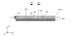
- FIG. 1 is a cross-sectional view schematically showing lighting device 100A_L.
- the illumination device 100A_L includes a light source LS and an optical laminate 100A. As will be described later, the lighting device 100A_L has a function of illuminating the front when the light source LS is on, and functions as a mirror when the light source LS is off.
- the light source LS is, for example, an LED device.
- a plurality of LED devices may be used as the light source LS.
- a plurality of LED devices are arranged, for example, in the X direction.
- the optical laminate 100A has a first principal surface and a second principal surface opposite to the first principal surface.
- the main surface on the upper side is the first main surface
- the main surface on the lower side is the second main surface.
- the lighting device 100A_L functions as a mirror, the first main surface is positioned on the viewer side (front side), and the second main surface is positioned on the side opposite to the viewer side (back side). .
- the optical laminate 100A receives light emitted from the light source LS, propagates the light in the Y direction, and emits the light in the Z direction. Therefore, the first main surface of the optical layered body 100A functions as a light exit surface.
- the light propagation direction has variations (distribution) from the Y direction
- the light emission direction also has variations (distribution) from the Z direction.
- a coupling optical system may be provided between the optical layered body 100A and the light source LS to efficiently guide the light emitted from the light source LS to the optical layered body 100A.
- the optical laminate 100A has a light guide layer 10 and a mirror layer 1.
- the light guide layer 10 includes a light receiving portion that receives light emitted from the light source LS, a third main surface 10b located on the first main surface side (that is, the light emission surface side), and a second main surface side (that is, the light emission surface side). and a fourth main surface 10c located on the opposite side to the surface side.
- the light receiving portion of the light guide layer 10 is a side surface (light receiving side surface) 10a of the light guide layer 10 on the light source LS side.
- the third main surface 10b of the light guide layer 10 is the optical layered body 100A. It is a 1st main surface.
- the mirror layer 1 is arranged on the fourth main surface 10 c side of the light guide layer 10 .
- the mirror layer 1 has light reflectivity.
- the mirror layer 1 includes a layer made of a material that specularly reflects light, as will be described later.
- the optical laminate 100A further has a light distribution control structure having a plurality of internal spaces IS.
- a plurality of internal spaces IS of the light distribution control structure form an interface that directs part of the light propagating in the light guide layer 10 toward the first principal surface by total internal reflection (TIR).
- Each internal space IS has a first inclined surface ISa that directs part of the light propagating in the light guide layer 10 toward the first principal surface by total internal reflection, and a second inclined surface ISa opposite to the first inclined surface ISa. and a surface ISb.
- a light distribution control structure having a plurality of internal spaces IS is formed within the light guide layer 10 .
- the light distribution control structure formed in the light guide layer 10 may be referred to as a "first light distribution control structure".
- the internal space IS is typically a gap (air cavity) filled with air.
- the visible light transmittance and haze value of the light guide layer 10 can be controlled.
- the visible light transmittance of the light guide layer 10 is, for example, 60% or more, preferably 80% or more.
- the haze value of the light guide layer 10 is, for example, less than 30%, preferably less than 10%.
- light with a wavelength of 380 nm or more and 780 nm or less is defined as visible light.
- Visible light transmittance and haze value can be measured using, for example, a haze meter (manufactured by Murakami Color Research Laboratory: trade name HM-150).
- the ratio of the area of the plurality of internal spaces IS to the area of the light guide layer 10 is 1% or more and 80% or less. and more preferably 1% or more and 50% or less. From the viewpoint of obtaining a low haze value, the occupied area ratio of the internal space IS is preferably 30% or less, more preferably 10% or less.
- FIG. 2 is a plan view schematically showing the illumination device 100A_L.
- FIG. 3 is a cross-sectional view schematically showing the internal space IS, and
- FIG. 4 is a plan view schematically showing the internal space IS.
- the plurality of internal spaces IS can be arranged discretely, for example, in the light guide direction (Y direction) of the light guide layer 10 and in a direction intersecting the light guide direction.
- the discrete arrangement may or may not have periodicity (regularity) in at least one direction.
- a plurality of internal spaces IS having substantially the same shape and curved surfaces convex in the same direction are arranged in the light guide direction (Y direction) of the light guide plate 10 and perpendicular to the light guide direction. are arranged discretely and periodically in the direction (X direction).
- the pitch Px of the internal spaces IS in the X direction is preferably 10 ⁇ m or more and 500 ⁇ m or less
- the pitch Py of the internal spaces IS in the Y direction is preferably 10 ⁇ m or more and 500 ⁇ m or less.
- an internal space IS is further provided that is arranged with a 1/2 pitch shift in each of the Y and X directions.
- the first inclined surface ISa forms a convex curved surface toward the light source LS when viewed from above in the direction normal to the first principal surface of the optical layered body 100A.
- the light source LS When a plurality of LED devices arranged in the X direction are used as the light source LS, the light emitted from each LED device spreads in the Y direction.
- the first inclined surface ISa having a curved surface acts more uniformly on light. Note that when a coupling optical system is provided between the light source LS and the light receiving side surface 10a of the light guide layer 10 so that highly parallel light (light with a small spread in the Y direction) is incident, the first inclined surface ISa may be parallel to the X direction.
- the discrete internal spaces IS for example, internal spaces such as grooves (for example, triangular prisms) extending in the X direction may be used.
- the cross-sectional shape of the internal space IS (the cross-sectional shape perpendicular to the X direction in FIG. 1 and parallel to the YZ plane) is, for example, the first main surface side of the optical layered body 100A (Z direction).
- the inclination angle ⁇ a of the first inclined surface ISa on the light source LS side is, for example, 10° or more and 70° or less. If the angle of inclination ⁇ a is less than 10°, the controllability of the light distribution may deteriorate, and the light extraction efficiency may also deteriorate. On the other hand, if the inclination angle ⁇ a exceeds 70°, it may become difficult to process the film that constitutes the light guide layer 10, for example.
- the inclination angle ⁇ b of the second inclined surface ISb is, for example, 50° or more and 100° or less. If the tilt angle ⁇ b is less than 50°, stray light may occur in an unintended direction. On the other hand, if the inclination angle ⁇ b exceeds 100°, it may become difficult to process the film forming the light guide layer 10, for example.
- the cross-sectional shape of the internal space IS is not limited to the triangular shape illustrated here, and may be trapezoidal or the like.
- the two-dimensional size of the internal space IS is defined by the length L and width W of the internal space IS.
- the length L of the internal space IS is preferably 10 ⁇ m or more and 500 ⁇ m or less, for example.
- the width W of the internal space IS is preferably 1 ⁇ m or more and 100 ⁇ m or less, for example.
- the length L of the internal space IS is, for example, twice or more the width W of the internal space IS.
- the height H (see FIG. 3) of the internal space IS is preferably, for example, 1 ⁇ m or more and 100 ⁇ m or less.
- the lighting device 100A_L when the light source LS is turned on, the light emitted from the light source LS and propagating through the light guide layer 10 is controlled by the light distribution control structure. Illumination can be performed by directing the light toward one main surface (light LRa in FIG. 1).
- the illumination device 100A_L When the light source LS is turned off, the illumination device 100A_L functions as a mirror by reflecting (specularly reflecting) the external light incident on the optical laminate 100A on the mirror layer 1, as shown in FIG. It works (light LRb in FIG. 5).
- the lighting device 100A_L can be used as a lighting device when the light source LS is on, and can be used as a mirror when the light source LS is off. That is, the lighting device 100A_L can switch between a mode (illumination mode) functioning as a lighting device and a mode (mirror mode) functioning as a mirror. Therefore, it can be said that the lighting device 100A_L is a design lighting device for a completely new application.
- the lighting device 100A_L has a light distribution control structure having a plurality of internal spaces IS (that is, using total internal reflection), the efficiency of light utilization is high, and the light guide layer 10 (optical laminate It is possible to realize high transparency (visible light transmittance) and low haze value of the body 100A except for the mirror layer 1).
- the visible light transmittance of the light guide layer 10 is preferably 60% or more, and the haze value of the light guide layer 10 is is preferably less than 30%.
- the illumination device 100A_L As a device that functions as both a lighting device and a mirror, it is conceivable to adopt a configuration in which a light source is arranged on the back of a half mirror. In this configuration, when the light source is on, illumination is performed by the light transmitted through the half mirror among the light emitted from the light source. Moreover, in this configuration, the half mirror functions as a mirror by reflecting external light when the light source is turned off. However, in this configuration, since the light reflectance of the half mirror is low, the mirror image in the mirror mode becomes dark. Also, in the lighting mode, part of the light emitted from the light source is reflected by the half mirror, so the light utilization efficiency is low. On the other hand, the illumination device 100A_L according to the embodiment of the present invention has the above-described configuration, thereby suppressing darkening of the mirror image in the mirror mode and increasing the light utilization efficiency in the illumination mode. can be done.
- the illumination device 100A_L can avoid such problems.
- the light guide layer 10 can be made of a known material with high visible light transmittance.
- the light guide layer 10 is made of, for example, an acrylic resin such as polymethyl methacrylate (PMMA), a polycarbonate (PC) resin, a cycloolefin resin, or glass (for example, quartz glass, alkali-free glass, or borosilicate glass). be.
- the refractive index n GP of the light guide layer 10 is, for example, 1.40 or more and 1.80 or less. Unless otherwise specified, the refractive index refers to the refractive index measured with an ellipsometer at a wavelength of 550 nm.
- the thickness of the light guide layer 10 can be appropriately set according to the application.
- the thickness of the light guide layer 10 is, for example, 0.05 mm or more and 50 mm or less.
- the light guide layer 10 formed with a light distribution control structure having a plurality of internal spaces IS is formed by laminating a first film having no pattern and a second film having a desired fine pattern formed thereon, for example. or by bonding with an adhesive (including a pressure sensitive adhesive).
- Laser patterning, direct laser imaging, laser drilling, masked or maskless laser or electron beam irradiation are used to form the micropattern on the second film. Further, individual characteristics may be imparted by printing, inkjet printing, screen printing, or the like, and the material and refractive index value may be changed. Micro/nanodispensing, dosing, direct "writing”, discrete laser sintering, micro electrical discharge machining (micro EDM) or micromachining, micromolding, imprinting, embossing and the like can also be used.
- micro EDM micro electrical discharge machining
- a glass plate whose surface is plated with metal eg, aluminum plating or silver plating
- a metal plate eg, aluminum plate
- a reflective film having a multilayer structure made of resin can also be used.
- the light guide layer 10 and the mirror layer 1 can be bonded together via an adhesive layer, for example.
- adhesive is meant to include pressure-sensitive adhesives (also called adhesives).
- FIG. 6 is a cross-sectional view schematically showing lighting device 100B_L. The following description will focus on the differences between the lighting device 100B_L and the lighting device 100A_L shown in FIG.
- the optical layered body 100B included in the lighting device 100B_L differs from the optical layered body 100A of the lighting device 100A_L in that an antireflection layer 20 is further provided.
- the antireflection layer 20 is arranged on the third main surface 10b side of the light guide layer 10, that is, on the first main surface (light emission surface) side with respect to the light distribution control structure.
- the antireflection layer 20 is provided, so that surface reflection on the first main surface of the optical layered body 100B can be suppressed.
- the antireflection layer 20 for example, a multi-layer laminate composed of a plurality of thin films having different refractive indices can be used.
- Materials for the thin films forming the multilayer laminate include metal oxides, nitrides, fluorides, and the like.
- the antireflection layer 20 is preferably an alternate laminate of high refractive index layers and low refractive index layers.
- the refractive index of the high refractive index layer is, for example, 1.9 or more, preferably 2.0 or more.
- Materials for the high refractive index layer include titanium oxide, niobium oxide, zirconium oxide, tantalum oxide, zinc oxide, indium oxide, indium tin oxide (ITO), and antimony-doped tin oxide (ATO). Among them, titanium oxide or niobium oxide is preferable.
- the refractive index of the low refractive index layer is, for example, 1.6 or less, preferably 1.5 or less.
- Materials for the low refractive index layer include silicon oxide, titanium nitride, magnesium fluoride, barium fluoride, calcium fluoride, hafnium fluoride, and lanthanum fluoride. Among them, silicon oxide is preferred. In particular, it is preferable to alternately stack a niobium oxide (Nb 2 O 5 ) thin film as a high refractive index layer and a silicon oxide (SiO 2 ) thin film as a low refractive index layer.
- a medium refractive index layer having a refractive index of about 1.6 to 1.9 may be provided in addition to the low refractive index layer and the high refractive index layer.
- the film thicknesses of the high refractive index layer and the low refractive index layer are each about 5 nm or more and 200 nm or less, preferably about 15 nm or more and 150 nm or less.
- the film thickness of each layer may be designed so that the reflectance of visible light is reduced according to the refractive index, lamination structure, and the like.
- the method of forming the thin film that constitutes the antireflection layer 20 is not particularly limited, and either a wet coating method or a dry coating method may be used.
- a dry coating method such as vacuum deposition, CVD, sputtering, or electron beam deposition is preferable because a thin film having a uniform thickness can be formed.
- the sputtering method is preferable because it is excellent in uniformity of film thickness and easy to form a dense film.
- the antireflection layer described in JP-A-2020-52221 can be preferably used.
- the entire disclosure of Japanese Patent Application Laid-Open No. 2020-52221 is incorporated herein by reference.
- FIG. 7 is a cross-sectional view schematically showing the lighting device 100C_L. The following description will focus on the differences between the lighting device 100C_L and the lighting device 100A_L shown in FIG.
- the optical layered body 100C included in the lighting device 100C_L differs from the optical layered body 100A of the lighting device 100A_L in that an antifouling layer 30 is further provided.
- the antifouling layer 30 has water repellency and/or oil repellency (hydrophilicity).
- the antifouling layer 30 is arranged on the third main surface 10b side of the light guide layer 10, and is provided as the outermost layer on the first main surface (light exit surface) side of the optical layered body 100C.
- the illuminating device 100C_L is provided with the antifouling layer 30, so that the optical layered body 100C can be prevented from being soiled.
- the configuration of the antifouling layer 30 is appropriately selected according to the application.
- Antifouling layer 30 can be formed using a known material.
- a silicone-based compound or a fluorine-containing compound is preferable.
- fluorine-containing compounds are excellent in water repellency and can exhibit high antifouling properties, and fluorine-based polymers containing a perfluoropolyether skeleton are particularly preferable.
- perfluoropolyethers having a rigidly parallel main chain structure are particularly preferred.
- the structural unit of the main chain skeleton of the perfluoropolyether is preferably an optionally branched perfluoroalkylene oxide having 1 to 4 carbon atoms, such as perfluoromethylene oxide (--CF 2 O--). , perfluoroethylene oxide (--CF 2 CF 2 O--), perfluoropropylene oxide (--CF 2 CF 2 CF 2 O--), perfluoroisopropylene oxide (--CF(CF 3 )CF 2 O--), etc. be done.
- the thickness of the antifouling layer 30 is preferably 3 nm or more and 15 nm or less, more preferably 3 nm or more and 10 nm or less.
- the method for forming the antifouling layer 30 may be a physical vapor deposition method such as vapor deposition or sputtering, a chemical vapor deposition method, a reverse coating method, a die coating method, a wet coating method such as a gravure coating method, or the like, depending on the material. can be used.
- the antifouling layer described in JP-A-2020-067582 can be preferably used.
- the entire disclosure of Japanese Patent Application Laid-Open No. 2020-067582 is incorporated herein by reference.
- An antireflection layer may be arranged on the antifouling layer 30 on the light guide layer 10 side (between the antifouling layer 30 and the light guide layer 10).
- FIG. 8 is a cross-sectional view schematically showing the illumination device 100D_L. The following description will focus on the differences between the lighting device 100D_L and the lighting device 100A_L shown in FIG.
- the optical layered body 100D included in the lighting device 100D_L differs from the optical layered body 100A of the lighting device 100A_L in that the polarization selective reflection layer 40 is further provided.
- the polarization selective reflection layer 40 is arranged on the third main surface 10b side of the light guide layer 10, that is, on the first main surface (light emission surface) side with respect to the light distribution control structure.
- the polarization selective reflection layer 40 selectively reflects light in a specific polarization state (polarization direction) and transmits light in other polarization states.
- the polarization selective reflection layer 40 selectively reflects one of two mutually orthogonal polarized components contained in light and transmits the other polarized component.
- the illuminating device 100D_L is provided with the polarization selective reflection layer 40, it is possible to selectively emit light in a certain polarization state (polarization direction) from the first main surface of the optical laminate 100D in the illumination mode. Therefore, it functions as a polarized illumination device.
- the lighting device 100D_L that can function as a polarized lighting device in this way can be suitably used for, for example, the following uses.
- the applicant of the present application has proposed a peeping prevention system capable of preventing peeping from the outside in International Publication No. 2021/200722.
- the peep prevention system includes a display device and a partition that separates a space in which display is provided by the display device from the surroundings.
- the display device has a first polarizing layer in front of the display surface with a first absorption axis parallel to a first direction (eg one of the horizontal and vertical directions).
- the partition has a translucent portion through which the inside of the space described above can be seen.
- the transparent portion of the partition has a second polarizing layer disposed on the space side of the transparent substrate and having a second absorption axis parallel to a second direction (eg, the other of the horizontal direction and the vertical direction). With such a configuration, it is possible to prevent the display by the display device from being peeped from the outside.
- the lighting device 100D_L By arranging the lighting device 100D_L in a room (for example, a conference room) in which this peep prevention system is used, the visibility of the lighting from the outside in the lighting mode can be reduced.
- the lighting device 100D_L is used as a backlight for a liquid crystal display device, the light extraction efficiency can be further improved.
- the polarization selective reflection layer 40 for example, a multilayer optical film such as DBEF manufactured by 3M can be used.
- the degree of polarization of the polarization selective reflection layer 40 is, for example, 90% or more, preferably 99% or more.
- an antireflection layer 20 may be provided on the polarization selective reflection layer 40 (on the first main surface side of the polarization selective reflection layer 40).
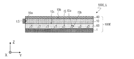
- FIG. 10 is a cross-sectional view schematically showing the illumination device 100E_L. The following description will focus on the differences between the illumination device 100E_L and the illumination device 100D_L shown in FIG.
- the optical layered body 100E included in the lighting device 100E_L differs from the optical layered body 100D of the lighting device 100D_L in that a direction changing layer 60 is further provided.
- the direction changing layer 60 is provided on the third main surface 10b side of the light guide layer 10 .
- the light distribution control structure having a plurality of internal spaces IS is formed in the direction conversion layer 60, not in the light guide layer 10.
- the light distribution control structure formed in the direction changing layer 60 may be referred to as a "second light distribution control structure".
- the light distribution control structure (second light distribution control structure) of the illumination device 100E_L also directs part of the light propagating in the light guide layer 10 toward the first main surface.
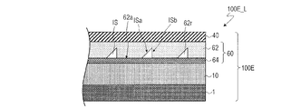
- FIG. 11 shows an example of a specific configuration of the direction changing layer 60 on which the light distribution control structure is formed.
- the direction changing layer 60 includes a shaping film 62 having a fifth main surface 62a having a plurality of recesses 62r, and an adhesive layer disposed on the fifth main surface 62a side of the shaping film 62. 64.
- the adhesive layer 64 is located between the shaping film 62 and the light guide layer 10 , and the light guide layer 10 and the shaping film 62 are adhered by the adhesive layer 64 .
- a plurality of internal spaces IS are defined by a plurality of recesses 62 r of the shaping film 62 and the adhesive layer 64 .
- the shaping film 62 for forming the internal space IS can be produced, for example, by the method described in JP-T-2013-524288. Specifically, for example, the surface of a polymethyl methacrylate (PMMA) film is coated with a lacquer (for example, Fine Cure RM-64 manufactured by Sanyo Chemical Industries, Ltd.), and an optical pattern is embossed on the film surface containing the lacquer. , and then curing the lacquer to form the shaped film 62A.
- PMMA polymethyl methacrylate
- a lacquer for example, Fine Cure RM-64 manufactured by Sanyo Chemical Industries, Ltd.
- the thickness of the adhesive layer 64 is, for example, 0.1 ⁇ m or more and 100 ⁇ m or less, preferably 0.3 ⁇ m or more and 100 ⁇ m or less, and more preferably 0.5 ⁇ m or more and 50 ⁇ m or less.
- the refractive index of the adhesive layer 64 is preferably 1.42 or more and 1.60 or less, more preferably 1.47 or more and 1.58 or less.
- the refractive index of the adhesive layer 64 is preferably close to the refractive index of the light guide layer 10 or the shaping film 62, and the absolute value of the difference in refractive index is preferably 0.2 or less.
- adhesives include rubber-based adhesives, acrylic-based adhesives, silicone-based adhesives, epoxy-based adhesives, cellulose-based adhesives, and polyester-based adhesives. These adhesives may be used alone or in combination of two or more.
- the adhesive layer 64 can adhere without filling the concave portions 62r on the surface of the shaping film 62 .
- the adhesive described in International Publication No. 2021/167090, International Publication No. 2021/167091, or International Application PCT/JP2022/004554 by the present applicant is preferably used. be able to. The entire disclosure of these applications is incorporated herein by reference.
- the polyester-based adhesive described in International Application PCT/JP2022/004554 is preferred.
- the shaping film 62 and the polarization selective reflection layer 40 can be bonded together by an adhesive layer.
- FIG. 10 illustrates a configuration in which the direction changing layer 60 is provided on the third main surface 10b side of the light guide layer 10, but the arrangement of the direction changing layer 60 is not limited to this.
- FIG. 12 shows another example of the arrangement of the redirecting layer 60. As shown in FIG. In the example shown in FIG. 12, the direction changing layer 60 is provided on the fourth main surface 10c side of the light guide layer 10 (that is, between the light guide layer 10 and the mirror layer 1).
- FIG. 13 is a cross-sectional view schematically showing the lighting device 100F_L. The following description will focus on the differences between the lighting device 100F_L and the lighting device 100E_L shown in FIG.
- the optical layered body 100F included in the lighting device 100F_L differs from the optical layered body 100E of the lighting device 100E_L in that a quarter-wave plate 70 is further provided.
- the quarter-wave plate 70 is arranged between the polarization selective reflection layer 40 and the mirror layer 1, and more specifically, on the side of the fourth main surface 10c of the light guide layer 10 (that is, between the light guide layer 10 and the light guide layer 10). mirror layer 1).
- the quarter-wave plate 70 as described above is provided.
- Light that is, light that cannot be transmitted through the polarization selective reflection layer 40
- FIG. 13 shows an example in which the quarter-wave plate 70 is arranged on the fourth main surface 10c side of the light guide layer 10, the arrangement of the quarter-wave plate 70 is not limited to this.
- FIG. 14 shows another example of the arrangement of the quarter wave plate 70. As shown in FIG. In the example shown in FIG. 14, the quarter-wave plate 70 is arranged between the direction changing layer 60 and the polarization selective reflection layer 40 . In the arrangement illustrated in FIG. 13 and the arrangement illustrated in FIG. 14, quarter-wave plate 70 is optically equivalent and functions similarly.
- the light distribution control structure in which part of the light propagating in the light guide layer 10 is directed toward the first main surface side was exemplified. may be configured to face the second main surface side.
- the luminous intensity distribution control structure (first luminous intensity distribution control structure) formed in the light guide layer 10 can internally transmit part of the light propagating in the light guide layer 10 like the illumination device 100A_L shown in FIG. It may have a plurality of internal spaces IS that form an interface directed toward the second principal surface by total reflection.
- the cross-sectional shape of these internal spaces IS is, for example, a triangle having an apex angle on the second main surface side ( ⁇ Z direction in FIG. 15) of the optical layered body 100A.
- the light distribution control structure (second light distribution control structure) formed in the direction changing layer 60 controls part of the light propagating in the light guide layer 10 as in the lighting device 100E_L shown in FIG. It may have a plurality of internal spaces IS forming an interface directed toward the second principal surface by reflection.
- the cross-sectional shape of these internal spaces IS is, for example, a triangle having an apex angle on the second main surface side ( ⁇ Z direction in FIG. 16) of the optical layered body 100A.
- the light directed toward the second main surface is reflected by the mirror layer 1 to be directed toward the first main surface and emitted from the first main surface. Therefore, even when the light distribution control structure is configured to direct part of the light propagating in the light guide layer 10 toward the second main surface, illumination can be performed favorably.
- FIG. 17 is a cross-sectional view schematically showing the lighting device 100G_L. The following description will focus on the differences between the lighting device 100G_L and the lighting device 100E_L shown in FIG.
- the optical laminate 100G included in the illumination device 100G_L further includes an optical coupling layer 80 provided between the light guide layer 10 and the direction changing layer 60.
- the optical coupling layer 80 has a plurality of low refractive index regions 80 a having a refractive index n C smaller than the refractive index n GP of the light guide layer 10 .
- Each low refractive index region 80a is formed in a dot shape with a size of 1 ⁇ m or more and 1000 ⁇ m or less, for example.
- the illumination device 100G_L is provided with the light coupling layer 80 having the plurality of low refractive index regions 80a, so that the light propagating through the light guide layer 10 can be more selectively and efficiently guided to the direction conversion layer 60. can. Further, by adjusting the arrangement density of the plurality of low refractive index regions 80a, the uniformity of emitted light can be controlled. For example, the uniformity of light can be improved by arranging the low refractive index regions 80a densely on the light source LS side and sparsely spaced away from the light source LS.
- the polarization selective reflection layer 40 of the illumination device 100G_L may be omitted as shown in FIG.
- the effect of providing the optical coupling layer 80 can be obtained even in the configuration in which the polarization selective reflection layer 40 is omitted as shown in FIG.
- the direction changing layer 60 may be provided on the fourth main surface 10c side of the light guide layer 10 (that is, between the light guide layer 10 and the mirror layer 1). Even in the configuration in which the direction changing layer 60 is provided on the fourth main surface 10c side of the light guide layer 10, the light coupling layer 80 is provided between the light guide layer 10 and the direction changing layer 60, A similar effect can be obtained.
- the refractive index n C of the low refractive index region 80a is preferably from 1.05 to 1.30, more preferably from 1.05 to 1.25.
- the difference between the refractive index nGP of the light guide layer 10 and the refractive index nC of the low refractive index region 80a is preferably 0.20 or more, more preferably 0.23 or more, and still more preferably 0.25. That's it.
- the low refractive index region 80a having a refractive index n C of 1.30 or less can be, for example, a porous region having a void structure inside.
- the thickness of the low refractive index region 80a is, for example, 0.3 ⁇ m or more and 5 ⁇ m or less.
- the low refractive index region 80a When the low refractive index region 80a is a porous region, its porosity is preferably 35% by volume or more, more preferably 38% by volume or more, and particularly preferably 40% by volume or more. Within such a range, the low refractive index region 80a having a particularly low refractive index can be formed.
- the upper limit of the porosity is, for example, 90% by volume or less, preferably 75% by volume or less. Within such a range, the low refractive index region 80a having excellent strength can be obtained.
- the porosity is calculated by Lorentz-Lorenz's formula from refractive index values measured by an ellipsometer.
- the low refractive index region 80a for example, a low refractive index layer having a void structure disclosed in WO2019/146628 can be used.
- the entire disclosure of WO2019/146628 is incorporated herein by reference.
- the low refractive index regions 80a having a void structure are composed of substantially spherical particles such as silica particles, silica particles having micropores, hollow silica nanoparticles, fibrous particles such as cellulose nanofibers, alumina nanofibers, silica nanofibers, and the like. It may include particles, tabular particles such as nanoclays composed of bentonite, and the like.
- the low refractive index region 80a having a void structure can be a porous body configured by directly chemically bonding particles (for example, microporous particles) to each other. At least a part of the particles forming the low refractive index region 80a having a void structure may be bonded together via a small amount (for example, the mass of the particles or less) of one component of the binder.
- the porosity and refractive index n C of the low refractive index region 80a can be adjusted by the particle size, particle size distribution, etc. of the particles forming the low refractive index region 80a.
- Methods for obtaining the low refractive index region 80a having a void structure include, for example, JP-A-2010-189212, JP-A-2008-040171, JP-A-2006-011175, International Publication No. 2004/113966, and Methods described in those references are included. All of the disclosures of JP-A-2010-189212, JP-A-2008-040171, JP-A-2006-011175, and International Publication No. 2004/113966 are incorporated herein by reference.
- a silica porous body can be suitably used as the low refractive index region 80a having a void structure.
- a silica porous body is produced, for example, by the following method. a silicon compound; hydrolyzable silanes and/or silsesquioxane, and a method of hydrolyzing and polycondensing at least one of its partial hydrolyzate and dehydration condensate; porous particles and/or hollow fine particles; method, method of generating an airgel layer using the springback phenomenon, pulverizing the gel-like silicon compound obtained by the sol-gel method, and chemically pulverizing the resulting pulverized microporous particles with a catalyst or the like. and a method using a combined pulverized gel.
- the low refractive index region 80a is not limited to the silica porous body, nor is the manufacturing method limited to the exemplified manufacturing method, and may be manufactured by any manufacturing method.
- Silsesquioxane is a silicon compound having (RSiO 1.5 , R is a hydrocarbon group) as a basic structural unit, and is strictly different from silica having SiO 2 as a basic structural unit.
- a porous material containing silsesquioxane as a basic structural unit is also referred to herein as a silica porous material or a silica-based porous material, since it has a network structure crosslinked with silica in common.
- the silica porous body can be composed of microporous particles of a gel-like silicon compound bonded together.
- pulverized bodies of the gelled silicon compound can be mentioned.
- the silica porous body can be formed, for example, by coating a base material with a coating liquid containing a pulverized gel-like silicon compound.
- the pulverized gel-like silicon compound can be chemically bonded (for example, siloxane bond) by the action of a catalyst, light irradiation, heating, or the like.
- FIG. 19 is a cross-sectional view schematically showing the lighting device 100H_L. The following description will focus on the differences between the lighting device 100H_L and the lighting device 100G_L shown in FIG.
- the optical laminate 100H included in the illumination device 100H_L includes a first region R1 in which the light distribution control structure exists (that is, the internal space IS is formed) and a first region R1 in which the light distribution control structure does not exist ( That is, it has a second region R2 in which the internal space IS is not formed.
- the first region R1 and the second region R2 are arranged so as to define a predetermined pattern when viewed from above in the direction normal to the first main surface.
- the "design” includes characters, numbers, symbols, pictures, patterns, combinations thereof, and the like.
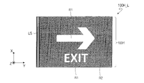
- FIG. 20 shows an example of arrangement of the first region R1 and the second region R2.
- FIG. 20 shows a state in which the lighting device 100H_L is lit.
- the first region R1 in which the light distribution control structure exists is a region (light emitting region) that emits light in the lighting state
- the second region R2 in which the light distribution control structure does not exist substantially It is a region (non-light-emitting region) that does not emit light at all.
- the pattern defined by the first area R1 and the second area R2 is not limited to the one illustrated in FIG.
- the first region R1 in which the light distribution control structure exists and the second region R2 in which the light distribution control structure does not exist are arranged so as to define a predetermined pattern. , can emit light in a predetermined pattern in the lighting mode. Therefore, illumination (light emission) rich in design and entertainment can be realized.
- the first region R1 and the second region R2 are arranged so as to define the characters "EXIT" and the arrow. Therefore, the illumination device 100H_L can be used as a mirror in the mirror mode during normal times, and can be used as a guide light indicating the evacuation direction in the illumination mode in an emergency. Always putting up emergency guidance signs (guide lights) may impair the appearance of facilities and buildings. obtain. In this way, the lighting device 100H_L can be used for more practical purposes depending on the design, and can normally function as a mirror. can.
- FIG. 21 is a cross-sectional view schematically showing the illumination device 100I_L. The following description will focus on the differences between the lighting device 100I_L and the lighting device 100G_L shown in FIG.
- the optical laminate 100I included in the illumination device 100I_L has a first region R1' where the optical coupling layer 80 exists and a second region R2' where the optical coupling layer 80 does not exist.
- the first region R1' and the second region R2' are arranged so as to define a predetermined pattern when viewed from above in the direction normal to the first main surface.
- the first region R1′ where the light coupling layer 80 exists (that is, the low refractive index region 80a is formed)
- the light propagating in the light guide layer 10 is totally reflected by the light coupling layer 80, resulting in a light distribution control structure. (internal space IS) becomes difficult to reach. Therefore, the first region R1' in which the optical coupling layer 80 exists is a region (low-luminance light-emitting region) that emits light (or substantially does not emit light) with relatively low luminance in the lighting state.
- the second region R2' where the optical coupling layer 80 does not exist is a region that emits light with relatively high luminance in the lighting state (high luminance light emitting region).
- the first region R1′ in which the optical coupling layer 80 exists and the second region R2′ in which the optical coupling layer 80 does not exist are arranged so as to define a predetermined pattern.
- light can be emitted so that a predetermined pattern can be visually recognized in the illumination mode. Therefore, illumination (light emission) rich in design and entertainment can be realized.
- a coating method or a printing method can be suitably used.
- a coating method a mask having a predetermined pattern may be used for coating.
- a printing method a plate-type printing method such as gravure printing may be used, or a plateless printing method such as inkjet printing may be used.
- the illumination device according to the embodiment of the present invention is a device for a completely new application that is used by switching between illumination mode and mirror mode, and can be used as a building member, for example.
- Reference Signs List 1 mirror layer 10 light guide layer 10a light receiving side surface of light guide layer 10b third main surface of light guide layer 10c fourth main surface of light guide layer 20 antireflection layer 30 antifouling layer 40 polarization selective reflection layer 60 direction changing layer 62 Shaping film 62r Concave portion of shaping film 64 Adhesive layer 70 Quarter wave plate 80 Optical coupling layer 80a Low refractive index regions 100A, 100B, 100C, 100D, 100E, 100F Optical laminate 100G, 100H, 100I Optical laminate 100A_L, 100B_L, 100C_L Lighting device 100D_L, 100E_L, 100F_L Lighting device 100G_L, 100H_L, 100I_L Lighting device IS Internal space ISa First inclined surface ISb Second inclined surface LS Light source R1, R1' First region R2, R2' Second region
Landscapes
- Physics & Mathematics (AREA)
- Engineering & Computer Science (AREA)
- General Engineering & Computer Science (AREA)
- General Physics & Mathematics (AREA)
- Optics & Photonics (AREA)
- Planar Illumination Modules (AREA)
Abstract
光学積層体(100A)は、第1主面と、第1主面とは反対側の第2主面とを有する。光学積層体(100A)は、光源(LS)から出射された光を受ける受光部(10a)と、第1主面側の第3主面(10b)と、第2主面側の第4主面(10c)とを有する導光層(10)と、導光層(10)の第4主面(10c)側に配置された光反射性を有するミラー層(1)と、複数の内部空間(IS)を有する配光制御構造であって、複数の内部空間(IS)は、導光層(10)内を伝搬する光の一部を内部全反射によって第1主面側または第2主面側に向ける界面を形成する、配光制御構造と、を有する。
Description
本発明は、光学積層体および照明装置に関する。
鏡を使用する際の利便性を向上させる目的で、使用者を照らすための照明装置を備え付けられた照明装置付き鏡が知られている。照明装置付き鏡は、例えば、特許文献1および2に開示されている。
特許文献1に開示されている照明装置付き鏡では、鏡の背面側に配置された光源部から前方斜め上方に出射した光が、鏡の上方に配置された反射部材によって前方斜め下方に反射されることによって照明が行われる。特許文献2に開示されている照明装置付き鏡では、鏡の外周縁部にリング状の透光部が設けられており、鏡の背面側に配置されたLED光源から発せられた光が、透光部から前面側に出射することによって照明が行われる。
特許文献1および2に開示されているような従来の照明装置付き鏡では、鏡に備え付けられた照明装置は、あくまでも鏡の使用者を照らすためのものである。
本発明の実施形態は、意匠性または娯楽性に富んだ照明装置およびそのような照明装置に好適に用いられる光学積層体を提供することを目的とする。
本発明の実施形態によると、以下の項目に記載の解決手段が提供される。
[項目1]
第1主面と、第1主面とは反対側の第2主面とを有する光学積層体であって、
光源から出射された光を受ける受光部と、前記第1主面側の第3主面と、前記第2主面側の第4主面とを有する導光層と、
前記導光層の前記第4主面側に配置された光反射性を有するミラー層と、
複数の内部空間を有する配光制御構造であって、前記複数の内部空間は、前記導光層内を伝搬する光の一部を内部全反射によって前記第1主面側または前記第2主面側に向ける界面を形成する、配光制御構造と、
を有する光学積層体。
第1主面と、第1主面とは反対側の第2主面とを有する光学積層体であって、
光源から出射された光を受ける受光部と、前記第1主面側の第3主面と、前記第2主面側の第4主面とを有する導光層と、
前記導光層の前記第4主面側に配置された光反射性を有するミラー層と、
複数の内部空間を有する配光制御構造であって、前記複数の内部空間は、前記導光層内を伝搬する光の一部を内部全反射によって前記第1主面側または前記第2主面側に向ける界面を形成する、配光制御構造と、
を有する光学積層体。
[項目2]
前記配光制御構造に対して前記第1主面側に配置された偏光選択反射層をさらに有する、項目1に記載の光学積層体。
前記配光制御構造に対して前記第1主面側に配置された偏光選択反射層をさらに有する、項目1に記載の光学積層体。
[項目3]
前記偏光選択反射層と前記ミラー層との間に配置された1/4波長板をさらに有する、項目2に記載の光学積層体。
前記偏光選択反射層と前記ミラー層との間に配置された1/4波長板をさらに有する、項目2に記載の光学積層体。
[項目4]
前記配光制御構造に対して前記第1主面側に配置された反射防止層をさらに有する、項目1から3に記載の光学積層体。
前記配光制御構造に対して前記第1主面側に配置された反射防止層をさらに有する、項目1から3に記載の光学積層体。
[項目5]
撥水性および/または撥油性を有する防汚層を前記第1主面側の最外層としてさらに有する、項目1から4に記載の光学積層体。
撥水性および/または撥油性を有する防汚層を前記第1主面側の最外層としてさらに有する、項目1から4に記載の光学積層体。
[項目6]
前記配光制御構造は、前記複数の内部空間が前記導光層内に形成されている第1配光制御構造を含む、項目1から5に記載の光学積層体。
前記配光制御構造は、前記複数の内部空間が前記導光層内に形成されている第1配光制御構造を含む、項目1から5に記載の光学積層体。
[項目7]
前記配光制御構造は、前記複数の内部空間が前記導光層の前記第3主面側または前記第4主面側に設けられた方向変換層に形成されている第2配光制御構造を含む、項目1から5に記載の光学積層体。
前記配光制御構造は、前記複数の内部空間が前記導光層の前記第3主面側または前記第4主面側に設けられた方向変換層に形成されている第2配光制御構造を含む、項目1から5に記載の光学積層体。
[項目8]
前記導光層と前記方向変換層との間に設けられた光結合層をさらに有し、
前記光結合層は、前記導光層の屈折率よりも小さい屈折率を有する複数の低屈折率領域を有する、項目7に記載の光学積層体。
前記導光層と前記方向変換層との間に設けられた光結合層をさらに有し、
前記光結合層は、前記導光層の屈折率よりも小さい屈折率を有する複数の低屈折率領域を有する、項目7に記載の光学積層体。
[項目9]
前記第1主面に対する法線方向から平面視したとき、前記配光制御構造が存在する第1領域と、前記配光制御構造が存在しない第2領域とが所定の図柄を規定するように配置されている、項目1から8に記載の光学積層体。
前記第1主面に対する法線方向から平面視したとき、前記配光制御構造が存在する第1領域と、前記配光制御構造が存在しない第2領域とが所定の図柄を規定するように配置されている、項目1から8に記載の光学積層体。
[項目10]
前記第1主面に対する法線方向から平面視したとき、前記光結合層が存在する第1領域と、前記光結合層が存在しない第2領域とが所定の図柄を規定するように配置されている、項目8に記載の光学積層体。
前記第1主面に対する法線方向から平面視したとき、前記光結合層が存在する第1領域と、前記光結合層が存在しない第2領域とが所定の図柄を規定するように配置されている、項目8に記載の光学積層体。
[項目11]
項目1から10のいずれか1項に記載の光学積層体と、
前記受光部に向けて光を出射する光源と、
を備える、照明装置。
項目1から10のいずれか1項に記載の光学積層体と、
前記受光部に向けて光を出射する光源と、
を備える、照明装置。
本発明の実施形態によると、意匠性または娯楽性に富んだ照明装置およびそのような照明装置に好適に用いられる光学積層体を提供することができる。
以下、図面を参照しながら、本発明の実施形態による光学積層体および照明装置を説明する。なお、本発明の実施形態による光学積層体および照明装置は、以下の説明で例示するものに限定されない。
[光学積層体および照明装置の構成]
図1を参照しながら、本発明の実施形態による照明装置100A_Lを説明する。図1は、照明装置100A_Lを模式的に示す断面図である。
図1を参照しながら、本発明の実施形態による照明装置100A_Lを説明する。図1は、照明装置100A_Lを模式的に示す断面図である。
照明装置100A_Lは、図1に示すように、光源LSと、光学積層体100Aとを備える。照明装置100A_Lは、後述するように、光源LSが点灯している状態において前方を照明する機能を奏する一方で、光源LSが消灯している状態においては、鏡として機能する。
光源LSは、例えばLED装置である。光源LSとして、複数のLED装置が用いられてもよい。複数のLED装置は、例えばX方向に配列される。
光学積層体100Aは、第1主面と、第1主面とは反対側の第2主面とを有する。図1において上側の主面が第1主面であり、下側の主面が第2主面である。照明装置100A_Lが鏡として機能している状態において、第1主面は、視認者側(前面側)に位置し、第2主面は、視認者側とは反対側(背面側)に位置する。
光学積層体100Aは、光源LSから出射された光を受け、Y方向に光を伝搬させるとともにZ方向に光を出射させる。従って、光学積層体100Aの第1主面が光出射面として機能する。もちろん、光の伝搬方向はY方向からばらつき(分布)を有し、光の出射方向もZ方向からばらつき(分布)を有している。なお、光学積層体100Aと光源LSとの間に、光源LSから出射された光を効率的に光学積層体100Aに導くための結合光学系を設けてもよい。
光学積層体100Aは、導光層10と、ミラー層1とを有する。
導光層10は、光源LSから出射された光を受ける受光部と、第1主面側(つまり光出射面側)に位置する第3主面10bと、第2主面側(つまり光出射面側とは反対側)に位置する第4主面10cとを有する。図示している例では、導光層10の受光部は、導光層10の光源LS側の側面(受光側面)10aである。また、図示している例では、光学積層体100Aの第1主面側の最表面に導光層10が位置しているので、導光層10の第3主面10bが光学積層体100Aの第1主面である。
ミラー層1は、導光層10の第4主面10c側に配置されている。ミラー層1は、光反射性を有する。ミラー層1は、後述するように、光を鏡面反射する材料から形成された層を含んでいる。
光学積層体100Aは、複数の内部空間ISを有する配光制御構造をさらに有する。配光制御構造が有する複数の内部空間ISは、導光層10内を伝搬する光の一部を内部全反射(TIR)によって第1主面側に向ける界面を形成する。各内部空間ISは、導光層10内を伝搬する光の一部を内部全反射によって第1主面側に向ける第1傾斜面ISaと、第1傾斜面ISaとは反対側の第2傾斜面ISbとを有している。
例示している光学積層体100Aにおいては、複数の内部空間ISを有する配光制御構造は、導光層10内に形成されている。本願明細書では、導光層10内に形成された配光制御構造を「第1配光制御構造」と呼ぶことがある。
内部空間ISの断面形状、大きさ、配置密度および分布を調整することによって、光学積層体100Aの第1主面から出射する光の配光分布を制御することができる。内部空間ISは、典型的には、内部に空気が充填された空隙部(エアキャビティ)である。
また、内部空間ISの断面形状、大きさ、配置密度および分布を調整することによって、導光層10の可視光透過率およびヘイズ値を制御することができる。導光層10の可視光透過率は、例えば60%以上であり、好ましくは80%以上である。導光層10のヘイズ値は、例えば30%未満であり、好ましくは10%未満である。ここでは、波長が380nm以上780nm以下の光を可視光とする。可視光透過率およびヘイズ値は、例えば、ヘイズメータ(村上色彩技術研究所製:商品名HM-150)を用いて測定することができる。
光学積層体100Aを第1主面の法線方向から平面視したときに、導光層10の面積に占める複数の内部空間ISの面積の割合(占有面積率)は、1%以上80%以下であることが好ましく、1%以上50%以下であることがさらに好ましい。低いヘイズ値を得る観点からは、内部空間ISの占有面積率は、30%以下が好ましく、10%以下がさらに好ましい。
図2、図3および図4を参照しながら、内部空間ISの形状および配置の例を説明する。図2は、照明装置100A_Lを模式的に示す平面図である。図3は、内部空間ISを模式的に示す断面図であり、図4は、内部空間ISを模式的に示す平面図である。
図2に示すように、複数の内部空間ISは、例えば、導光層10の導光方向(Y方向)および導光方向に交差する方向に離散的に配置され得る。離散的な配置は、少なくとも1つの方向において周期性(規則性)を有してもよいし、規則性を有しなくてもよい。ただし、量産性の観点からは、複数の内部空間ISが一様に配置されることが好ましい。例えば、図2に示した例では、実質的に同一の形状で同一の方向に凸な曲面を有する複数の内部空間ISが、導光板10の導光方向(Y方向)および導光方向に直交する方向(X方向)に離散的かつ周期的に配置されている。このとき、内部空間ISのX方向のピッチPxは、例えば10μm以上500μm以下であることが好ましく、内部空間ISのY方向のピッチPyは、例えば10μm以上500μm以下であることが好ましい。図2に示した例では、Y方向およびX方向のそれぞれに2分の1ピッチずれて配置された内部空間ISがさらに設けられている。
図2に示したように、光学積層体100Aの第1主面に対する法線方向から平面視したとき、第1傾斜面ISaは光源LS側に凸な曲面を形成している。光源LSとして、X方向に配列された複数のLED装置が用いられる場合、各LED装置から出射される光はY方向に対して広がりを有するので、第1傾斜面ISaが光源LS側に凸な曲面を有している方が、第1傾斜面ISaが光に対して均一に作用する。なお、光源LSと導光層10の受光側面10aとの間に結合光学系を設け、平行度の高い光(Y方向に対する広がりが小さい光)を入射させるようにした場合は、第1傾斜面ISaはX方向に平行であってもよい。また、離散的な内部空間ISに代えて、例えば、X方向に延びる溝(例えば三角柱)のような内部空間であってもよい。
図3に示すように、内部空間ISの断面形状(図1におけるX方向に垂直でYZ面に平行な断面の形状)は、例えば、光学積層体100Aの第1主面側(図1におけるZ方向)に頂角を有する三角形である。光源LS側の第1傾斜面ISaの傾斜角度θaは、例えば、10°以上70°以下である。傾斜角度θaが10°未満であると配光の制御性が低下し、光取り出し効率も低下することがある。一方、傾斜角度θaが70°を超えると、例えば導光層10を構成するフィルムの加工が困難になることがある。また、第2傾斜面ISbの傾斜角度θbは、例えば、50°以上100°以下である。傾斜角度θbが50°未満であると、意図しない方向に迷光が発生することがある。一方、傾斜角度θbが100°を超えると、例えば導光層10を構成するフィルムの加工が困難になることがある。なお、内部空間ISの断面形状は、ここで例示したような三角形に限られず、台形等であってもよい。
図4に示すように、内部空間ISの二次元的な大きさは、内部空間ISの長さLおよび幅Wによって規定される。内部空間ISの長さLは、例えば10μm以上500μm以下であることが好ましい。内部空間ISの幅Wは、例えば1μm以上100μm以下であることが好ましい。内部空間ISの長さLは、例えば、内部空間ISの幅Wの2倍以上である。また、内部空間ISの高さH(図3参照)は、光取り出し効率の観点からは、例えば1μm以上100μm以下であることが好ましい。
上述したように、本発明の実施形態による照明装置100A_Lは、光源LSが点灯している状態においては、光源LSから発せられて導光層10内を伝搬する光を、配光制御構造によって第1主面側に向けることにより、照明を行うことができる(図1中の光LRa)。また、照明装置100A_Lは、光源LSが消灯している状態においては、図5に示すように、光学積層体100Aに入射した外部光をミラー層1で反射(鏡面反射)することにより、鏡として機能する(図5中の光LRb)。このように、本発明の実施形態による照明装置100A_Lは、光源LSの点灯状態においては照明装置として使用され、光源LSの消灯状態においては鏡として使用され得る。つまり、照明装置100A_Lは、照明装置として機能する態様(照明モード)と、鏡として機能する態様(ミラーモード)とを切り替えることができる。そのため、照明装置100A_Lは、まったく新しい用途の意匠性照明装置であるといえる。
また、照明装置100A_Lは、複数の内部空間ISを有する(つまり内部全反射を利用する)配光制御構造を有しているので、光の利用効率が高く、また、導光層10(光学積層体100Aのミラー層1を除く部分)の高い透明性(可視光透過率)および低いヘイズ値を実現することができる。導光層10を介してミラー層1(ミラー層1に映る像)を見る観点からは、導光層10の可視光透過率が60%以上であることが好ましく、導光層10のヘイズ値が30%未満であることが好ましい。
なお、照明装置としても鏡としても機能する装置として、ハーフミラーの背面に光源が配置された構成を採用することが考えられる。この構成では、光源が点灯している状態においては、光源から発せられた光のうち、ハーフミラーを透過した光によって照明が行われる。また、この構成は、光源が消灯している状態においては、ハーフミラーが外部光を反射することによって、鏡として機能する。しかしながら、この構成では、ハーフミラーによる光反射率が低いので、ミラーモードにおける鏡像が暗くなる。また、照明モードでは、光源から発せられた光の一部がハーフミラーで反射されるので、光の利用効率が低くなる。これに対し、本発明の実施形態による照明装置100A_Lは、上述した構成を有していることにより、ミラーモードにおいて鏡像が暗くなることを抑制し、また、照明モードにおける光利用効率を高くすることができる。
また、照明装置としても鏡としても機能する装置として、フロントライトと呼ばれる照明装置が鏡の前面に配置された構成を採用することが考えられる。しかしながら、この構成では、フロントライトの導光板に形成された光を取り出すための構造(例えばドット状パターン)が視認されることによってミラーモードにおける鏡像の品位が低下するおそれがある。これに対し、本発明の実施形態による照明装置100A_Lでは、そのような問題の発生を回避することができる。
[導光層、ミラー層の好ましい構成の例]
導光層10は、可視光に対する透過率が高い公知の材料で形成され得る。導光層10は、例えば、ポリメチルメタクリレート(PMMA)等のアクリル系樹脂、ポリカーボネート(PC)系樹脂、シクロオレフィン系樹脂、ガラス(例えば、石英ガラス、無アルカリガラス、ホウケイ酸ガラス)で形成される。導光層10の屈折率nGPは、例えば、1.40以上1.80以下である。なお、屈折率は、特にことわらない限り、波長550nmにおいてエリプソメーターで測定した屈折率をいう。導光層10の厚さは用途に応じて適宜設定され得る。導光層10の厚さは、例えば、0.05mm以上50mm以下である。
導光層10は、可視光に対する透過率が高い公知の材料で形成され得る。導光層10は、例えば、ポリメチルメタクリレート(PMMA)等のアクリル系樹脂、ポリカーボネート(PC)系樹脂、シクロオレフィン系樹脂、ガラス(例えば、石英ガラス、無アルカリガラス、ホウケイ酸ガラス)で形成される。導光層10の屈折率nGPは、例えば、1.40以上1.80以下である。なお、屈折率は、特にことわらない限り、波長550nmにおいてエリプソメーターで測定した屈折率をいう。導光層10の厚さは用途に応じて適宜設定され得る。導光層10の厚さは、例えば、0.05mm以上50mm以下である。
複数の内部空間ISを有する配光制御構造が形成された導光層10は、例えば、パターンが形成されていない第1フィルムと、所望の微細パターンが形成された第2フィルムとを、ラミネーション法で貼り合わせるか、または接着剤(感圧接着剤を含む)により接着することで作製される。
第2フィルムへの微細パターンの形成には、レーザパターニング、ダイレクトレーザイメージング、レーザドリル、マスクによるまたはマスクレスのレーザまたは電子ビーム照射が用いられる。また印刷、インクジェット印刷、スクリーン印刷等によって個別の特性を付与して、材料や屈折率値を変更してもよい。マイクロ/ナノディスペンス、ドージング、ダイレクト「書込み」、離散的レーザ焼結、マイクロ放電加工(マイクロEDM)、またはマイクロマシニング、マイクロ成形、インプリンティング、エンボス加工およびこれらに類するものを用いることもできる。
ミラー層1としては、表面に金属めっき(例えばアルミニウムめっきや銀めっき)が施されたガラス板や、金属板(例えばアルミニウム板)を用いることができる。また、ミラー層1として、樹脂から形成された多層膜構造を有する反射フィルムを用いることもできる。
導光層10とミラー層1とは、例えば接着剤層を介して貼り合わされ得る。ここで、「接着剤」は、感圧接着剤(粘着剤とも呼ぶ)を含む意味である。
[反射防止層を有する構成]
図6を参照しながら、本発明の実施形態による他の照明装置100B_Lを説明する。図6は、照明装置100B_Lを模式的に示す断面図である。以下では、照明装置100B_Lが図1に示した照明装置100A_Lと異なる点を中心に説明を行う。
図6を参照しながら、本発明の実施形態による他の照明装置100B_Lを説明する。図6は、照明装置100B_Lを模式的に示す断面図である。以下では、照明装置100B_Lが図1に示した照明装置100A_Lと異なる点を中心に説明を行う。
図6に示すように、照明装置100B_Lが備える光学積層体100Bは、反射防止層20をさらに備える点において、照明装置100A_Lの光学積層体100Aと異なっている。反射防止層20は、導光層10の第3主面10b側、つまり、配光制御構造に対して第1主面(光出射面)側に配置されている。
照明装置100B_Lでは、反射防止層20が設けられていることにより、光学積層体100Bの第1主面における表面反射を抑制することができる。
反射防止層20としては、例えば、屈折率の異なる複数の薄膜からなる多層積層体を用いることができる。多層積層体を構成する薄膜の材料としては、金属の酸化物、窒化物、フッ化物等が挙げられる。
反射防止層20は、好ましくは、高屈折率層と低屈折率層の交互積層体である。高屈折率層の屈折率は、例えば1.9以上であり、好ましくは2.0以上である。高屈折率層の材料としては、酸化チタン、酸化ニオブ、酸化ジルコニウム、酸化タンタル、酸化亜鉛、酸化インジウム、酸化インジウムスズ(ITO)、アンチモンドープ酸化スズ(ATO)等が挙げられる。中でも、酸化チタンまたは酸化ニオブが好ましい。低屈折率層の屈折率は、例えば1.6以下であり、好ましくは1.5以下である。低屈折率層の材料としては、酸化ケイ素、窒化チタン、フッ化マグネシウム、フッ化バリウム、フッ化カルシウム、フッ化ハフニウム、フッ化ランタン等が挙げられる。中でも酸化ケイ素が好ましい。特に、高屈折率層としての酸化ニオブ(Nb2O5)薄膜と、低屈折率層としての酸化ケイ素(SiO2)薄膜とを交互に積層することが好ましい。低屈折率層と高屈折率層に加えて、屈折率1.6~1.9程度の中屈折率層が設けられてもよい。
高屈折率層および低屈折率層の膜厚は、それぞれ、5nm以上200nm以下程度であり、15nm以上150nm以下程度が好ましい。屈折率や積層構成等に応じて、可視光の反射率が小さくなるように、各層の膜厚を設計すればよい。
反射防止層20を構成する薄膜の成膜方法は特に限定されず、ウェットコーティング法、ドライコーティング法のいずれでもよい。膜厚が均一な薄膜を形成できることから、真空蒸着、CVD、スパッタ、電子線蒸着等のドライコーティング法が好ましい。中でも、膜厚の均一性に優れ、緻密な膜を形成しやすいことから、スパッタ法が好ましい。例えば特開2020-52221号公報に記載の反射防止層を好適に用いることができる。特開2020-52221号公報の開示内容のすべてを参照により本明細書に援用する。
[防汚層を有する構成]
図7を参照しながら、本発明の実施形態によるさらに他の照明装置100C_Lを説明する。図7は、照明装置100C_Lを模式的に示す断面図である。以下では、照明装置100C_Lが図1に示した照明装置100A_Lと異なる点を中心に説明を行う。
図7を参照しながら、本発明の実施形態によるさらに他の照明装置100C_Lを説明する。図7は、照明装置100C_Lを模式的に示す断面図である。以下では、照明装置100C_Lが図1に示した照明装置100A_Lと異なる点を中心に説明を行う。
図7に示すように、照明装置100C_Lが備える光学積層体100Cは、防汚層30をさらに備える点において、照明装置100A_Lの光学積層体100Aと異なっている。防汚層30は、撥水性および/または撥油性(親水性)を有する。防汚層30は、導光層10の第3主面10b側に配置されており、光学積層体100Cの第1主面(光出射面)側の最外層として設けられている。
照明装置100C_Lでは、防汚層30が設けられていることにより、光学積層体100Cへの汚れの付着を防止することができる。
防汚層30の構成は、用途に応じて、適宜選択される。防汚層30は、公知の材料を用いて形成され得る。防汚層30を構成する材料としては、シリコーン系化合物またはフッ素含有化合物が好ましい。中でも、フッ素含有化合物は撥水性に優れ、高い防汚性を発揮でき、特にパーフルオロポリエーテル骨格を含有するフッ素系ポリマーが好ましい。防汚性を高める観点から、剛直に並列可能な主鎖構造を有するパーフルオロポリエーテルが特に好ましい。パーフルオロポリエーテルの主鎖骨格の構造単位としては、炭素数1~4の分枝を有していてもよいパーフルオロアルキレンオキシドが好ましく、例えば、パーフルオロメチレンオキシド、(-CF2O-)、パーフルオロエチレンオキシド(-CF2CF2O-)、パーフルオロプロピレンオキシド(-CF2CF2CF2O-)、パーフルオロイソプロピレンオキシド(-CF(CF3)CF2O-)等が挙げられる。
防汚層30の厚さは、好ましくは3nm以上15nm以下であり、より好ましくは3nm以上10nm以下である。
防汚層30の形成方法は、材料に応じて、蒸着、スパッタリング等の物理的気相成長法、化学的気相成長法、リバースコート法、ダイコート法、グラビアコート法等の湿式コーティング法等を用いることができる。例えば、特開2020-067582号公報に記載の防汚層を好適に用いることができる。特開2020-067582号公報の開示内容のすべてを参照により本明細書に援用する。
なお、防汚層30の導光層10側(防汚層30と導光層10との間)に反射防止層が配置されてもよい。
[偏光選択反射層を備える構成]
図8を参照しながら、本発明の実施形態によるさらに他の照明装置100D_Lを説明する。図8は、照明装置100D_Lを模式的に示す断面図である。以下では、照明装置100D_Lが図1に示した照明装置100A_Lと異なる点を中心に説明を行う。
図8を参照しながら、本発明の実施形態によるさらに他の照明装置100D_Lを説明する。図8は、照明装置100D_Lを模式的に示す断面図である。以下では、照明装置100D_Lが図1に示した照明装置100A_Lと異なる点を中心に説明を行う。
図8に示すように、照明装置100D_Lが備える光学積層体100Dは、偏光選択反射層40をさらに備える点において、照明装置100A_Lの光学積層体100Aと異なっている。偏光選択反射層40は、導光層10の第3主面10b側、つまり、配光制御構造に対して第1主面(光出射面)側に配置されている。偏光選択反射層40は、特定の偏光状態(偏光方向)の光を選択的に反射し、他の偏光状態の光を透過させる。例えば、偏光選択反射層40は、光に含まれる、互いに直交する2つの偏光成分のうち、一方の偏光成分を選択的に反射し、他方の偏光成分を透過させる。
照明装置100D_Lは、偏光選択反射層40が設けられていることにより、照明モードにおいて、光学積層体100Dの第1主面からある偏光状態(偏光方向)の光を選択的に出射することができるので、偏光照明装置として機能する。このように偏光照明装置として機能し得る照明装置100D_Lは、例えば、以下の用途に好適に用いることができる。
本願出願人は、国際公開第2021/200722号に、外部からの覗き見を防止することができる覗き見防止システムを提案している。この覗き見防止システムは、表示装置と、表示装置によって表示が提供される空間を周囲と区切る間仕切りとを含む。表示装置は、第1方向(例えば水平方向および鉛直方向の一方)に平行な第1吸収軸を有する第1偏光層を表示面の前面に有する。間仕切りは、上述した空間内を見ることができる透光部を有する。間仕切りの透光部は、透明基板の空間側に配置され、第2方向(例えば水平方向および鉛直方向の他方)に平行な第2吸収軸を有する第2偏光層を有する。このような構成により、表示装置による表示が外部から覗き見されることを防止することができる。
この覗き見防止システムが用いられた部屋(例えば会議室)内に照明装置100D_Lを配置すると、照明モードにおける照明の外部からの視認性を低下させることができる。
さらに、照明装置100D_Lを液晶表示装置用のバックライトとして用いる場合、光取り出し効率のいっそうの向上を図ることができる。
偏光選択反射層40としては、例えば、3M社製のDBEFのような多層光学フィルムを用いることができる。偏光選択反射層40の偏光度は、例えば90%以上であり、好ましくは99%以上である。
なお、図9に示すように、偏光選択反射層40上(偏光選択反射層40の第1主面側)に反射防止層20が設けられてもよい。
[偏光選択反射層を備える他の構成]
図10を参照しながら、本発明の実施形態によるさらに他の照明装置100E_Lを説明する。図10は、照明装置100E_Lを模式的に示す断面図である。以下では、照明装置100E_Lが図8に示した照明装置100D_Lと異なる点を中心に説明を行う。
図10を参照しながら、本発明の実施形態によるさらに他の照明装置100E_Lを説明する。図10は、照明装置100E_Lを模式的に示す断面図である。以下では、照明装置100E_Lが図8に示した照明装置100D_Lと異なる点を中心に説明を行う。
図10に示すように、照明装置100E_Lが備える光学積層体100Eは、方向変換層60をさらに備える点において、照明装置100D_Lの光学積層体100Dと異なっている。方向変換層60は、導光層10の第3主面10b側に設けられている。
照明装置100E_Lでは、複数の内部空間ISを有する配光制御構造は、導光層10内にではなく、方向変換層60に形成されている。本願明細書では、方向変換層60に形成された配光制御構造を「第2配光制御構造」と呼ぶことがある。照明装置100E_Lの配光制御構造(第2配光制御構造)も、導光層10内を伝搬する光の一部を第1主面側に向ける。
図11に、配光制御構造が形成された方向変換層60の具体的な構成の例を示す。図11に示す例では、方向変換層60は、複数の凹部62rを有する第5主面62aを有する賦形フィルム62と、賦形フィルム62の第5主面62a側に配置された接着剤層64とから構成されている。接着剤層64は、賦形フィルム62と導光層10との間に位置しており、接着剤層64によって導光層10と賦形フィルム62とが接着されている。複数の内部空間ISは、賦形フィルム62の複数の凹部62rと接着剤層64とによって画定されている。
内部空間ISを形成するための賦形フィルム62は、例えば、特表2013-524288号公報に記載の方法により作製することができる。具体的には、例えば、ポリメタクリル酸メチル(PMMA)フィルムの表面をラッカー(例えば三洋化成工業社製ファインキュアー RM-64)でコーティングし、当該ラッカーを含むフィルム表面上に光学パターンをエンボス加工し、その後ラッカーを硬化させることによって賦形フィルム62Aを作製することができる。
接着剤層64の厚さは、例えば0.1μm以上100μm以下であり、0.3μm以上100μm以下が好ましく、0.5μm以上50μm以下がさらに好ましい。接着剤層64の屈折率は、好ましくは1.42以上1.60以下であり、より好ましくは1.47以上1.58以下である。また、接着剤層64の屈折率は、導光層10または賦形フィルム62の屈折率と近いことが好ましく、屈折率の差の絶対値が0.2以下であることが好ましい。
接着剤の具体例としては、ゴム系接着剤、アクリル系接着剤、シリコーン系接着剤、エポキシ系接着剤、セルロース系接着剤、ポリエステル系接着剤が挙げられる。これらの接着剤は単独でも良いし、2種以上の組み合わせでも良い。
接着剤層64は、賦形フィルム62の表面の凹部62rを埋めることなく接着できることが好ましい。接着剤層64の形成に好適な接着剤としては、本出願人による国際公開第2021/167090号、国際公開第2021/167091号または国際出願PCT/JP2022/004554に記載の接着剤を好適に用いることができる。これらの出願の開示内容のすべてを本明細書に援用する。特に、国際出願PCT/JP2022/004554に記載のポリエステル系接着剤が好ましい。
なお、ここでは図示していないが、賦形フィルム62と偏光選択反射層40とは、接着剤層によって貼り合わされ得る。
また、図10には、方向変換層60が導光層10の第3主面10b側に設けられる構成を例示したが、方向変換層60の配置はこれに限定されない。図12に、方向変換層60の配置の他の例を示す。図12に示す例では、方向変換層60は、導光層10の第4主面10c側に(つまり導光層10とミラー層1との間に)設けられている。
[偏光選択反射層に加えて1/4波長板を備える構成]
図13を参照しながら、本発明の実施形態によるさらに他の照明装置100F_Lを説明する。図13は、照明装置100F_Lを模式的に示す断面図である。以下では、照明装置100F_Lが図10に示した照明装置100E_Lと異なる点を中心に説明を行う。
図13を参照しながら、本発明の実施形態によるさらに他の照明装置100F_Lを説明する。図13は、照明装置100F_Lを模式的に示す断面図である。以下では、照明装置100F_Lが図10に示した照明装置100E_Lと異なる点を中心に説明を行う。
図13に示すように、照明装置100F_Lが備える光学積層体100Fは、1/4波長板70をさらに備える点において、照明装置100E_Lの光学積層体100Eと異なっている。1/4波長板70は、偏光選択反射層40とミラー層1との間に配置されており、より具体的には、導光層10の第4主面10c側(つまり導光層10とミラー層1との間)に配置されている。
照明装置100F_Lでは、上述したような1/4波長板70が設けられていることにより、配光制御構造によって第1主面側に向けられた光のうち、偏光選択反射層40で反射された光(つまり偏光選択反射層40を透過できなかった光)を、偏光選択反射層40を透過するような偏光状態にする(元の偏光方向と直交する偏光方向にする)ことができるので、光の利用効率を高くすることができる。
1/4波長板70としては、公知の種々の1/4波長板を用いることができる。なお、図13には、1/4波長板70が導光層10の第4主面10c側に配置されている例を示したが、1/4波長板70の配置はこれに限定されない。図14に、1/4波長板70の配置の他の例を示す。図14に示す例では、1/4波長板70は、方向変換層60と偏光選択反射層40との間に配置されている。図13に例示した配置と、図14に例示した配置とで、1/4波長板70は光学的に等価であり、同様に機能する。
[配光制御構造の他の例]
これまでの説明では、導光層10内を伝搬する光の一部を第1主面側に向ける配光制御構造を例示したが、配光制御構造は、導光層10内を伝搬する光の一部を第2主面側に向けるように構成されてもよい。
これまでの説明では、導光層10内を伝搬する光の一部を第1主面側に向ける配光制御構造を例示したが、配光制御構造は、導光層10内を伝搬する光の一部を第2主面側に向けるように構成されてもよい。
例えば、導光層10内に形成された配光制御構造(第1配光制御構造)は、図15に示す照明装置100A_Lのように、導光層10内を伝搬する光の一部を内部全反射によって第2主面側に向ける界面を形成する複数の内部空間ISを有していてもよい。これらの内部空間ISの断面形状は、例えば、光学積層体100Aの第2主面側(図15における-Z方向)に頂角を有する三角形である。
また、方向変換層60に形成された配光制御構造(第2配光制御構造)は、図16に示す照明装置100E_Lのように、導光層10内を伝搬する光の一部を内部全反射によって第2主面側に向ける界面を形成する複数の内部空間ISを有していてもよい。これらの内部空間ISの断面形状は、例えば、光学積層体100Aの第2主面側(図16における-Z方向)に頂角を有する三角形である。
このように構成された配光制御構造によって、第2主面側に向けられた光は、ミラー層1で反射されることによって第1主面側に向かい、第1主面から出射する。そのため、配光制御構造が、導光層10内を伝搬する光の一部を第2主面側に向けるように構成されている場合でも、照明を好適に行うことができる。
[その他の構成]
図17を参照しながら、本発明の実施形態によるさらに他の照明装置100G_Lを説明する。図17は、照明装置100G_Lを模式的に示す断面図である。以下では、照明装置100G_Lが図10に示した照明装置100E_Lと異なる点を中心に説明を行う。
図17を参照しながら、本発明の実施形態によるさらに他の照明装置100G_Lを説明する。図17は、照明装置100G_Lを模式的に示す断面図である。以下では、照明装置100G_Lが図10に示した照明装置100E_Lと異なる点を中心に説明を行う。
図17に示すように、照明装置100G_Lが備える光学積層体100Gは、導光層10と方向変換層60との間に設けられた光結合層80をさらに有する。光結合層80は、導光層10の屈折率nGPよりも小さい屈折率nCを有する複数の低屈折率領域80aを有する。各低屈折率領域80aは、例えば、1μm以上1000μm以下のサイズのドット状に形成されている。
照明装置100G_Lでは、複数の低屈折率領域80aを有する光結合層80が設けられていることにより、導光層10を伝搬する光をより選択的かつ効率的に方向変換層60に導くことができる。また、複数の低屈折率領域80aの配置密度を調整することにより、出射する光の均一性を制御することができる。例えば、低屈折率領域80aを、光源LS側において密で、光源LSから遠ざかるにつれて疎になるように配置することにより、光の均一性を向上させることができる。
なお、図18に示すように、照明装置100G_Lの偏光選択反射層40は省略されてもよい。光結合層80を設けることによる効果は、図18に示したように偏光選択反射層40が省略された構成においても得られる。また、方向変換層60は導光層10の第4主面10c側に(つまり導光層10とミラー層1との間に)設けられてもよい。方向変換層60が導光層10の第4主面10c側に設けられている構成においても、導光層10と方向変換層60との間に光結合層80が設けられていることにより、同様の効果が得られる。
低屈折率領域80aの屈折率nCは、1.05以上1.30以下であることが好ましく、1.05以上1.25以下であることがさらに好ましい。導光層10の屈折率nGPと低屈折率領域80aの屈折率nCとの差は、好ましくは0.20以上であり、より好ましくは0.23以上であり、さらに好ましくは0.25以上である。屈折率nCが1.30以下の低屈折率領域80aは、例えば、内部に空隙構造を有する多孔質領域であり得る。低屈折率領域80aの厚さは、例えば、0.3μm以上5μm以下である。
低屈折率領域80aが多孔質領域である場合、その空隙率は、好ましくは35体積%以上であり、より好ましくは38体積%以上であり、特に好ましくは40体積%以上である。このような範囲であれば、屈折率が特に低い低屈折率領域80aを形成することができる。空隙率の上限は、例えば、90体積%以下であり、好ましくは75体積%以下である。このような範囲であれば、強度に優れる低屈折率領域80aが得られる。空隙率は、エリプソメーターで測定した屈折率の値から、Lorentz‐Lorenz’s formula(ローレンツ-ローレンツの式)より算出される。
低屈折率領域80aについては、例えば、国際公開第2019/146628号に開示された空隙構造を有する低屈折率層を用いることができる。国際公開第2019/146628号の開示内容のすべてを参照により本願明細書に援用する。具体的には、空隙構造を有する低屈折率領域80aは、シリカ粒子、微細孔を有するシリカ粒子、シリカ中空ナノ粒子等の略球状粒子、セルロースナノファイバー、アルミナナノファイバー、シリカナノファイバー等の繊維状粒子、ベントナイトから構成されるナノクレイ等の平板状粒子等を含み得る。空隙構造を有する低屈折率領域80aは、粒子(例えば微細孔粒子)同士が直接的に化学的に結合して構成される多孔体であり得る。また、空隙構造を有する低屈折率領域80aを構成する粒子同士は、その少なくとも一部が、少量(例えば、粒子の質量以下)のバインダ一成分を介して結合していてもよい。低屈折率領域80aの空隙率および屈折率nCは、低屈折率領域80aを構成する粒子の粒径、粒径分布等により調整することができる。
空隙構造を有する低屈折率領域80aを得る方法としては、例えば、特開2010-189212号公報、特開2008-040171号公報、特開2006-011175号公報、国際公開第2004/113966号、およびそれらの参考文献に記載された方法が挙げられる。特開2010-189212号公報、特開2008-040171号公報、特開2006-011175号公報、国際公開第2004/113966号の開示内容のすべてを参照により本明細書に援用する。
空隙構造を有する低屈折率領域80aとして、シリカ多孔体を好適に用いることができる。シリカ多孔体は、例えば、以下の方法で製造される。ケイ素化合物;加水分解性シラン類および/またはシルセスキオキサン、ならびにその部分加水分解物および脱水縮合物の少なくともいずれか1つを加水分解および重縮合させる方法、多孔質粒子および/または中空微粒子を用いる方法、ならびにスプリングバック現象を利用してエアロゲル層を生成する方法、ゾルゲル法により得られたゲル状ケイ素化合物を粉砕し、得られた粉砕体である微細孔粒子同士を触媒等で化学的に結合させた粉砕ゲルを用いる方法、等が挙げられる。ただし、低屈折率領域80aは、シリカ多孔体に限定されず、製造方法も例示した製造方法に限定されず、どのような製造方法により製造しても良い。なお、シルセスキオキサンは、(RSiO1.5、Rは炭化水素基)を基本構成単位とするケイ素化合物であり、SiO2を基本構成単位とするシリカとは厳密には異なるが、シロキサン結合で架橋されたネットワーク構造を有する点でシリカと共通しているので、ここではシルセスキオキサンを基本構成単位として含む多孔体もシリカ多孔体またはシリカ系多孔体という。
シリカ多孔体は、互いに結合したゲル状ケイ素化合物の微細孔粒子から構成され得る。ゲル状ケイ素化合物の微細孔粒子としては、ゲル状ケイ素化合物の粉砕体が挙げられる。シリカ多孔体は、例えば、ゲル状ケイ素化合物の粉砕体を含む塗工液を、基材に塗工して形成され得る。ゲル状ケイ素化合物の粉砕体は、例えば、触媒の作用、光照射、加熱等により化学的に結合(例えば、シロキサン結合)し得る。
図19を参照しながら、本発明の実施形態によるさらに他の照明装置100H_Lを説明する。図19は、照明装置100H_Lを模式的に示す断面図である。以下では、照明装置100H_Lが図18に示した照明装置100G_Lと異なる点を中心に説明を行う。
図19に示すように、照明装置100H_Lが備える光学積層体100Hは、配光制御構造が存在する(つまり内部空間ISが形成されている)第1領域R1と、配光制御構造が存在しない(つまり内部空間ISが形成されていない)第2領域R2とを有する。第1領域R1と、第2領域R2とは、第1主面に対する法線方向から平面視したとき、所定の図柄を規定するように配置されている。ここで、「図柄」は、文字、数字、記号、絵柄、模様およびこれらの組み合わせ等を含む。なお、図示している例では、光学積層体100Hは光結合層80を有していないが、光結合層80を有していてもよい。
図20に、第1領域R1および第2領域R2の配置の例を示す。図20は、照明装置100H_Lが点灯している状態を示している。
図20に示すように、配光制御構造が存在する第1領域R1は、点灯状態において発光する領域(発光領域)であり、配光制御構造が存在しない第2領域R2は、点灯状態において実質的に発光しない領域(非発光領域)である。言うまでもないが、第1領域R1および第2領域R2によって規定される図柄は、図20に例示したものに限定されない。
このように、照明装置100H_Lでは、配光制御構造が存在する第1領域R1と、配光制御構造が存在しない第2領域R2とが、所定の図柄を規定するように配置されていることにより、照明モードにおいて所定の図柄状に光を発することができる。そのため、意匠性および娯楽性に富んだ照明(発光)を実現することができる。
また、図20に示した例では、第1領域R1および第2領域R2は、「EXIT」という文字および矢印を規定するように配置されている。そのため、照明装置100H_Lは、通常時にはミラーモードで鏡として使用し、緊急時には照明モードで避難方向を示す誘導灯として用いることができる。緊急時用の誘導標識(誘導灯)を常に掲げておくことは、施設や建物の美観を損なうおそれがあるが、照明装置100H_Lをこのように用いることにより、そのような美観の低下を防止し得る。このように、照明装置100H_Lは、図柄によってはより実用的な用途にも用いることができ、通常時には鏡として機能させ得るので、実用的な用途に用いる場合であっても美観を損なうことを防止できる。
図21を参照しながら、本発明の実施形態によるさらに他の照明装置100I_Lを説明する。図21は、照明装置100I_Lを模式的に示す断面図である。以下では、照明装置100I_Lが図18に示した照明装置100G_Lと異なる点を中心に説明を行う。
図21に示すように、照明装置100I_Lが備える光学積層体100Iは、光結合層80が存在する第1領域R1’と、光結合層80が存在しない第2領域R2’とを有する。第1領域R1’と、第2領域R2’とは、第1主面に対する法線方向から平面視したとき、所定の図柄を規定するように配置されている。
光結合層80が存在する(つまり低屈折率領域80aが形成されている)第1領域R1’では、導光層10内を伝搬する光が光結合層80での全反射により配光制御構造(内部空間IS)に届きにくくなる。そのため、光結合層80が存在する第1領域R1’は、点灯状態において比較的低い輝度で発光する(あるいは実質的に発光しない)領域(低輝度発光領域)である。これに対し、光結合層80が存在しない(つまり低屈折率領域80aが形成されていない)第2領域R2’は、点灯状態において比較的高い輝度で発光する領域(高輝度発光領域)である。
このように、照明装置100I_Lでは、光結合層80が存在する第1領域R1’と、光結合層80が存在しない第2領域R2’とが、所定の図柄を規定するように配置されていることにより、照明モードにおいて所定の図柄が視認されるように光を発することができる。そのため、意匠性および娯楽性に富んだ照明(発光)を実現することができる。
低屈折率領域80aを第1領域R1’に選択的に形成する方法としては、塗布法または印刷法を好適に用いることができる。塗布法を用いる場合、所定のパターンを有するマスクを用いて塗布を行えばよい。印刷法としては、グラビア印刷等の有版式の印刷法を用いてもよいし、インクジェット印刷等の無版式の印刷法を用いてもよい。
本発明の実施形態によると、意匠性または娯楽性に富んだ照明装置およびそのような照明装置に好適に用いられる光学積層体を提供することができる。本発明の実施形態による照明装置は、照明モードとミラーモードとを切り替えて使用される、まったく新しい用途の装置であり、例えば建築部材としても用いることができる。
1 ミラー層
10 導光層
10a 導光層の受光側面
10b 導光層の第3主面
10c 導光層の第4主面
20 反射防止層
30 防汚層
40 偏光選択反射層
60 方向変換層
62 賦形フィルム
62r 賦形フィルムの凹部
64 接着剤層
70 1/4波長板
80 光結合層
80a 低屈折率領域
100A、100B、100C、100D、100E、100F 光学積層体
100G、100H、100I 光学積層体
100A_L、100B_L、100C_L 照明装置
100D_L、100E_L、100F_L 照明装置
100G_L、100H_L、100I_L 照明装置
IS 内部空間
ISa 第1傾斜面
ISb 第2傾斜面
LS 光源
R1、R1’ 第1領域
R2、R2’ 第2領域
10 導光層
10a 導光層の受光側面
10b 導光層の第3主面
10c 導光層の第4主面
20 反射防止層
30 防汚層
40 偏光選択反射層
60 方向変換層
62 賦形フィルム
62r 賦形フィルムの凹部
64 接着剤層
70 1/4波長板
80 光結合層
80a 低屈折率領域
100A、100B、100C、100D、100E、100F 光学積層体
100G、100H、100I 光学積層体
100A_L、100B_L、100C_L 照明装置
100D_L、100E_L、100F_L 照明装置
100G_L、100H_L、100I_L 照明装置
IS 内部空間
ISa 第1傾斜面
ISb 第2傾斜面
LS 光源
R1、R1’ 第1領域
R2、R2’ 第2領域
Claims (11)
- 第1主面と、第1主面とは反対側の第2主面とを有する光学積層体であって、
光源から出射された光を受ける受光部と、前記第1主面側の第3主面と、前記第2主面側の第4主面とを有する導光層と、
前記導光層の前記第4主面側に配置された光反射性を有するミラー層と、
複数の内部空間を有する配光制御構造であって、前記複数の内部空間は、前記導光層内を伝搬する光の一部を内部全反射によって前記第1主面側または前記第2主面側に向ける界面を形成する、配光制御構造と、
を有する光学積層体。 - 前記配光制御構造に対して前記第1主面側に配置された偏光選択反射層をさらに有する、請求項1に記載の光学積層体。
- 前記偏光選択反射層と前記ミラー層との間に配置された1/4波長板をさらに有する、請求項2に記載の光学積層体。
- 前記配光制御構造に対して前記第1主面側に配置された反射防止層をさらに有する、請求項1から3のいずれか1項に記載の光学積層体。
- 撥水性および/または撥油性を有する防汚層を前記第1主面側の最外層としてさらに有する、請求項1から4のいずれか1項に記載の光学積層体。
- 前記配光制御構造は、前記複数の内部空間が前記導光層内に形成されている第1配光制御構造を含む、請求項1から5のいずれか1項に記載の光学積層体。
- 前記配光制御構造は、前記複数の内部空間が前記導光層の前記第3主面側または前記第4主面側に設けられた方向変換層に形成されている第2配光制御構造を含む、請求項1から5のいずれか1項に記載の光学積層体。
- 前記導光層と前記方向変換層との間に設けられた光結合層をさらに有し、
前記光結合層は、前記導光層の屈折率よりも小さい屈折率を有する複数の低屈折率領域を有する、請求項7に記載の光学積層体。 - 前記第1主面に対する法線方向から平面視したとき、前記配光制御構造が存在する第1領域と、前記配光制御構造が存在しない第2領域とが所定の図柄を規定するように配置されている、請求項1から8のいずれか1項に記載の光学積層体。
- 前記第1主面に対する法線方向から平面視したとき、前記光結合層が存在する第1領域と、前記光結合層が存在しない第2領域とが所定の図柄を規定するように配置されている、請求項8に記載の光学積層体。
- 請求項1から10のいずれか1項に記載の光学積層体と、
前記受光部に向けて光を出射する光源と、
を備える、照明装置。
Priority Applications (1)
| Application Number | Priority Date | Filing Date | Title |
|---|---|---|---|
| JP2023531792A JPWO2023276705A1 (ja) | 2021-06-29 | 2022-06-16 |
Applications Claiming Priority (2)
| Application Number | Priority Date | Filing Date | Title |
|---|---|---|---|
| JP2021107333 | 2021-06-29 | ||
| JP2021-107333 | 2021-06-29 |
Publications (1)
| Publication Number | Publication Date |
|---|---|
| WO2023276705A1 true WO2023276705A1 (ja) | 2023-01-05 |
Family
ID=84692346
Family Applications (1)
| Application Number | Title | Priority Date | Filing Date |
|---|---|---|---|
| PCT/JP2022/024180 Ceased WO2023276705A1 (ja) | 2021-06-29 | 2022-06-16 | 光学積層体および照明装置 |
Country Status (2)
| Country | Link |
|---|---|
| JP (1) | JPWO2023276705A1 (ja) |
| WO (1) | WO2023276705A1 (ja) |
Citations (6)
| Publication number | Priority date | Publication date | Assignee | Title |
|---|---|---|---|---|
| JP2015035252A (ja) * | 2011-11-30 | 2015-02-19 | シャープ株式会社 | 光源装置、面光源装置、表示装置および照明装置 |
| JP2015173066A (ja) * | 2014-03-12 | 2015-10-01 | 大日本印刷株式会社 | バックライト装置、液晶表示装置及び積層体 |
| JP2019061787A (ja) * | 2017-09-25 | 2019-04-18 | オムロン株式会社 | 表示装置及び液晶表示装置 |
| WO2019180676A1 (en) * | 2018-03-22 | 2019-09-26 | Nitto Denko Corporation | Optical device |
| WO2020230783A1 (ja) * | 2019-05-13 | 2020-11-19 | 大日本印刷株式会社 | バリアフィルム、それを用いた波長変換シート、及びそれを用いた表示装置 |
| JP2021093369A (ja) * | 2019-12-10 | 2021-06-17 | 三菱電機株式会社 | 照明装置および拡散体 |
-
2022
- 2022-06-16 JP JP2023531792A patent/JPWO2023276705A1/ja active Pending
- 2022-06-16 WO PCT/JP2022/024180 patent/WO2023276705A1/ja not_active Ceased
Patent Citations (6)
| Publication number | Priority date | Publication date | Assignee | Title |
|---|---|---|---|---|
| JP2015035252A (ja) * | 2011-11-30 | 2015-02-19 | シャープ株式会社 | 光源装置、面光源装置、表示装置および照明装置 |
| JP2015173066A (ja) * | 2014-03-12 | 2015-10-01 | 大日本印刷株式会社 | バックライト装置、液晶表示装置及び積層体 |
| JP2019061787A (ja) * | 2017-09-25 | 2019-04-18 | オムロン株式会社 | 表示装置及び液晶表示装置 |
| WO2019180676A1 (en) * | 2018-03-22 | 2019-09-26 | Nitto Denko Corporation | Optical device |
| WO2020230783A1 (ja) * | 2019-05-13 | 2020-11-19 | 大日本印刷株式会社 | バリアフィルム、それを用いた波長変換シート、及びそれを用いた表示装置 |
| JP2021093369A (ja) * | 2019-12-10 | 2021-06-17 | 三菱電機株式会社 | 照明装置および拡散体 |
Also Published As
| Publication number | Publication date |
|---|---|
| JPWO2023276705A1 (ja) | 2023-01-05 |
Similar Documents
| Publication | Publication Date | Title |
|---|---|---|
| JP7317800B2 (ja) | 光学デバイス | |
| CN111295606B (zh) | 光分布结构和元件,相关方法和用途 | |
| JP7560557B2 (ja) | 照明装置用導光部材、照明装置および建築部材 | |
| KR20030085590A (ko) | 전면발광 터치 패널 | |
| TW202012834A (zh) | 改良式光分佈元件 | |
| KR20020032374A (ko) | 도광판, 면광원 장치 및 반사형 액정 표시장치 | |
| WO2006093087A1 (ja) | 光拡散フィルムおよびこれを用いた面光源素子並びに液晶表示装置 | |
| US12210181B2 (en) | Light guide member for lighting device and lighting device | |
| TW201505847A (zh) | 積層體、積層體的製造方法、光源裝置用導光體及光源裝置 | |
| US20240230978A1 (en) | Light guide member for light emission device and light emission device | |
| WO2023276705A1 (ja) | 光学積層体および照明装置 | |
| JP2009258666A (ja) | 機能性部材、光学部品、バックライトユニット及び表示装置 | |
| JP2004227913A (ja) | 光学素子、その製造方法及び液晶表示装置 | |
| WO2023276836A1 (ja) | 照明装置用導光部材および照明装置 | |
| CN223155344U (zh) | 显示系统以及背光 | |
| KR20250078925A (ko) | 조명 장치 | |
| JP2005005062A (ja) | 面光源装置及びそれを用いた表示装置 | |
| WO2022244474A1 (ja) | 光学装置 | |
| JP2009294672A (ja) | 光学調整部材、並びに、それを備える照明装置及び液晶表示装置 | |
| KR20260021595A (ko) | 적층 필름 및 롤 | |
| WO2024252895A1 (ja) | 積層フィルム | |
| JP2023550917A (ja) | 自己整合バックライト反射板 | |
| JP2003131226A (ja) | 反射型液晶表示装置 | |
| JP2013045762A (ja) | 光学複合シート |
Legal Events
| Date | Code | Title | Description |
|---|---|---|---|
| 121 | Ep: the epo has been informed by wipo that ep was designated in this application |
Ref document number: 22832855 Country of ref document: EP Kind code of ref document: A1 |
|
| WWE | Wipo information: entry into national phase |
Ref document number: 2023531792 Country of ref document: JP |
|
| NENP | Non-entry into the national phase |
Ref country code: DE |
|
| 122 | Ep: pct application non-entry in european phase |
Ref document number: 22832855 Country of ref document: EP Kind code of ref document: A1 |