WO2023243365A1 - Laser device - Google Patents
Laser device Download PDFInfo
- Publication number
- WO2023243365A1 WO2023243365A1 PCT/JP2023/019655 JP2023019655W WO2023243365A1 WO 2023243365 A1 WO2023243365 A1 WO 2023243365A1 JP 2023019655 W JP2023019655 W JP 2023019655W WO 2023243365 A1 WO2023243365 A1 WO 2023243365A1
- Authority
- WO
- WIPO (PCT)
- Prior art keywords
- frequency
- optical comb
- laser
- ceo
- control circuit
- Prior art date
Links
- 230000003287 optical effect Effects 0.000 claims abstract description 160
- 238000001514 detection method Methods 0.000 claims abstract description 40
- 238000001228 spectrum Methods 0.000 claims description 78
- 238000012545 processing Methods 0.000 claims description 50
- 238000000034 method Methods 0.000 description 79
- 230000008569 process Effects 0.000 description 57
- 230000009977 dual effect Effects 0.000 description 42
- 238000005259 measurement Methods 0.000 description 38
- 230000004044 response Effects 0.000 description 29
- 101100301150 Arabidopsis thaliana RCD1 gene Proteins 0.000 description 22
- 101100096653 Arabidopsis thaliana SRO1 gene Proteins 0.000 description 22
- 238000010586 diagram Methods 0.000 description 18
- 230000008859 change Effects 0.000 description 17
- 101100412093 Schizosaccharomyces pombe (strain 972 / ATCC 24843) rec16 gene Proteins 0.000 description 8
- 238000004364 calculation method Methods 0.000 description 5
- 230000005284 excitation Effects 0.000 description 5
- 239000000470 constituent Substances 0.000 description 4
- 230000005684 electric field Effects 0.000 description 4
- 230000010354 integration Effects 0.000 description 4
- 238000004590 computer program Methods 0.000 description 3
- 230000004048 modification Effects 0.000 description 3
- 238000012986 modification Methods 0.000 description 3
- 239000013307 optical fiber Substances 0.000 description 3
- 239000004065 semiconductor Substances 0.000 description 3
- 238000006243 chemical reaction Methods 0.000 description 2
- 238000006073 displacement reaction Methods 0.000 description 2
- 238000007689 inspection Methods 0.000 description 2
- 230000002123 temporal effect Effects 0.000 description 2
- 238000007792 addition Methods 0.000 description 1
- 230000001174 ascending effect Effects 0.000 description 1
- 230000004888 barrier function Effects 0.000 description 1
- 230000008901 benefit Effects 0.000 description 1
- 230000001427 coherent effect Effects 0.000 description 1
- 210000001520 comb Anatomy 0.000 description 1
- 238000007796 conventional method Methods 0.000 description 1
- 239000006185 dispersion Substances 0.000 description 1
- 230000000694 effects Effects 0.000 description 1
- 238000005516 engineering process Methods 0.000 description 1
- 230000006870 function Effects 0.000 description 1
- 239000000463 material Substances 0.000 description 1
- 238000000691 measurement method Methods 0.000 description 1
- 238000002360 preparation method Methods 0.000 description 1
- 230000003595 spectral effect Effects 0.000 description 1
- 230000000087 stabilizing effect Effects 0.000 description 1
- 238000006467 substitution reaction Methods 0.000 description 1
Images


Classifications
-
- H—ELECTRICITY
- H01—ELECTRIC ELEMENTS
- H01S—DEVICES USING THE PROCESS OF LIGHT AMPLIFICATION BY STIMULATED EMISSION OF RADIATION [LASER] TO AMPLIFY OR GENERATE LIGHT; DEVICES USING STIMULATED EMISSION OF ELECTROMAGNETIC RADIATION IN WAVE RANGES OTHER THAN OPTICAL
- H01S3/00—Lasers, i.e. devices using stimulated emission of electromagnetic radiation in the infrared, visible or ultraviolet wave range
- H01S3/10—Controlling the intensity, frequency, phase, polarisation or direction of the emitted radiation, e.g. switching, gating, modulating or demodulating
- H01S3/13—Stabilisation of laser output parameters, e.g. frequency or amplitude
-
- H—ELECTRICITY
- H01—ELECTRIC ELEMENTS
- H01S—DEVICES USING THE PROCESS OF LIGHT AMPLIFICATION BY STIMULATED EMISSION OF RADIATION [LASER] TO AMPLIFY OR GENERATE LIGHT; DEVICES USING STIMULATED EMISSION OF ELECTROMAGNETIC RADIATION IN WAVE RANGES OTHER THAN OPTICAL
- H01S3/00—Lasers, i.e. devices using stimulated emission of electromagnetic radiation in the infrared, visible or ultraviolet wave range
- H01S3/23—Arrangements of two or more lasers not provided for in groups H01S3/02 - H01S3/22, e.g. tandem arrangements of separate active media
Definitions
- the present disclosure relates to a laser device.
- an optical frequency comb laser is a light source that outputs laser light in which pulse waveforms are arranged at equal intervals on the time axis and spectra are arranged at equal intervals on the frequency axis.
- Patent Document 1 discloses a coherent dual scanning laser system that is controlled to stabilize the difference in carrier envelope offset frequency (f CEO ) between two oscillators. Further, Patent Document 2 discloses an optical comb control method in which the difference between the carrier envelope offset frequencies (f CEO ) of two oscillators is controlled to be an integral multiple of the repetition frequency (f rep ).
- the present disclosure provides a laser device that outputs light that can be detected with high accuracy by a detector.
- a laser device includes a first optical comb laser, a second optical comb laser having a repetition frequency different from that of the first optical comb laser, and an output light from the first optical comb laser and an output light from the second optical comb laser. and a control circuit, the control circuit detecting a first CEO frequency, which is a carrier envelope offset frequency of the first optical comb laser, and a carrier envelope offset frequency of the second optical comb laser.
- a difference frequency which is the difference between the first CEO frequency and the second CEO frequency, is changed.
- FIG. 1 is a diagram schematically showing temporal changes in the electric field of an optical comb laser beam.
- FIG. 2 is a diagram schematically showing a frequency spectrum of an optical comb laser beam.
- FIG. 3 is a diagram schematically showing frequency spectra of two optical comb laser beams in a dual comb.
- FIG. 4 is a diagram schematically showing a frequency spectrum after interference in a dual comb.
- FIG. 5 is a diagram schematically showing an example of a laser device according to an embodiment.
- FIG. 6 is a flowchart showing the process of controlling ⁇ f CEO based on the lowest frequency mode in the frequency spectrum of the dual comb signal, among the operations of the laser device according to the embodiment.
- FIG. 7 is a diagram illustrating an example of an inappropriate frequency spectrum of a dual comb signal.
- FIG. 8 is a flowchart showing the process of controlling ⁇ f CEO based on the highest frequency mode in the frequency spectrum of the dual comb signal, among the operations of the laser device according to the embodiment.
- FIG. 9 is a diagram showing an example of an inappropriate frequency spectrum of a dual comb signal.
- FIG. 10 is a flowchart showing the process of controlling ⁇ f CEO based on the frequency interval in the frequency spectrum of the dual comb signal, among the operations of the laser device according to the embodiment.
- FIG. 11 is a diagram showing an example of an inappropriate frequency spectrum of a dual comb signal.
- FIG. 12 is a flowchart showing an example of the process of controlling ⁇ f CEO based on the frequency spectrum of the dual comb signal, among the operations of the laser device according to the embodiment.
- FIG. 13 is a flowchart showing an example of the process of controlling ⁇ f CEO based on the accuracy of the distance calculated from the dual comb signal, among the operations of the laser device according to the embodiment.
- FIG. 14 is a flowchart illustrating an example of a process for controlling ⁇ f CEO as a calibration before measurement among operations of the laser device according to the embodiment.
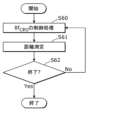
- FIG. 15 is a flowchart illustrating an example of a process for controlling ⁇ f CEO as feedback at any time among operations of the laser device according to the embodiment.
- FIG. 16 is a diagram showing the flow of processing in a modified example.
- Dual comb is a method in which two optical comb lasers are prepared, and their repetition frequencies are slightly shifted, allowing them to interfere with each other for measurement.
- two optical comb lasers whose repetition frequencies are f rep and f rep + ⁇ f rep , respectively, interfere with each other, thereby generating a beat.
- spectra with intervals of ⁇ f rep can be obtained. What is important here is that the spectrum of the optical comb laser before interference is in the THz region, which is the frequency of light, while the spectrum after interference is in the MHz region, which is the radio frequency.
- the response may vary depending on the value of ⁇ f CEO , which is the difference between the carrier envelope offset frequencies f CEO of the two optical comb lasers. There are cases where the frequency band is exceeded, making measurement difficult.
- a laser device includes a first optical comb laser, a second optical comb laser having a repetition frequency different from that of the first optical comb laser, and an output light from the first optical comb laser and an output light from the second optical comb laser. and a control circuit, the control circuit detecting a first CEO frequency, which is a carrier envelope offset frequency of the first optical comb laser, and a carrier envelope offset frequency of the second optical comb laser.
- a difference frequency which is the difference between the first CEO frequency and the second CEO frequency, is changed.
- the control circuit acquires second information regarding the highest frequency mode of the frequency spectrum of the interference light based on the output of the detection unit, and 2 information may be used to reduce the difference frequency.
- the control circuit acquires third information regarding a frequency interval of the frequency spectrum of the interference light based on the output of the detection unit, and the acquired third information
- the difference frequency may be changed using .
- the detection unit may detect interference between reflected light from an object of output light from the first optical comb laser and output light from the second optical comb laser.
- the laser device may include a signal processing circuit that detects light and calculates a distance to the object based on the output of the detection section.
- control circuit may change the differential frequency before calculating the distance.
- control circuit may change the differential frequency while calculating the distance.
- the laser device according to one aspect of the present disclosure may be configured by appropriately combining the constituent elements of the laser device according to each aspect described above.
- each figure is a schematic diagram and is not necessarily strictly illustrated. Therefore, for example, the scales and the like in each figure do not necessarily match. Further, in each figure, substantially the same configurations are denoted by the same reference numerals, and overlapping explanations will be omitted or simplified.
- ordinal numbers such as “first” and “second” do not mean the number or order of components, unless otherwise specified, and do not mean the number or order of components. It is used for the purpose of
- the optical comb laser beam is formed from a train of optical pulses generated at a repeating period T rep .
- the repetition period T rep is, for example, 1 ps or more and 100 ns or less.
- the full width at half maximum of each optical pulse is represented by ⁇ t.
- the full width at half maximum ⁇ t of each optical pulse is, for example, 10 fs or more and 100 ps or less.
- FIG. 2 is a diagram schematically showing the frequency spectrum of optical comb laser light.
- the horizontal axis represents the frequency
- the vertical axis represents the intensity of the optical comb laser beam.
- the optical comb laser beam has a comb-shaped frequency spectrum formed from a plurality of discrete equally spaced lines.
- the frequencies of the plurality of discrete equally spaced lines correspond to the resonance frequency of the longitudinal mode in the laser resonator.
- the repetition frequency f rep and the carrier envelope offset frequency f CEO may change slightly due to disturbances such as vibrations or temperature changes to the optical comb laser source. This is because vibrations change the circumferential length L of the laser cavity, and temperature changes can also change the group velocity v g and phase velocity v p via changes in the refractive index of the laser cavity.
- the repetition frequency f rep and the carrier envelope offset frequency f CEO are much lower than the optical frequency. Even a slight change in them can affect the identification of the mode frequency in the optical comb laser beam. For this reason, a conventional optical comb laser light source incorporates a modulation element that stabilizes the repetition frequency f rep and the carrier envelope offset frequency f CEO .
- the modulation element includes, for example, a piezoelectric element such as a piezo element for suppressing vibration, and/or a temperature adjustment element such as a Peltier element for suppressing temperature change.
- the modulation element may be provided outside the optical comb laser light source.
- a part of the optical comb laser beam is detected, and based on the detected part, the circumferential length L of the laser resonator is made constant using a piezo element and a Peltier element. Feedback will be provided.
- a part of the optical comb laser light is detected using a nonlinear optical effect, and the intensity of the excitation light input to the laser resonator is adjusted based on the detected part. Feedback is performed so that the nonlinearity within the laser resonator becomes constant.
- FIG. 3 is a diagram showing frequency spectra of a first optical comb laser and a second optical comb laser in a dual comb.
- f CEO1 is an example of the first CEO frequency and is the carrier envelope offset frequency of the first optical comb laser.
- f CEO2 is an example of the second CEO frequency, and is the carrier envelope offset frequency of the second optical comb laser.
- f rep1 is the repetition frequency of the first optical comb laser.
- the frequency interval of the frequency spectrum of the interference light is ⁇ f rep , which is the difference between the repetition frequencies of the first optical comb laser and the second optical comb laser.
- X in the figure represents a value from 0 to the lowest frequency mode.
- F max represents the response frequency band of the detector. As shown in FIG. 4, if the frequency spectrum of the interference light falls within F max , detection of the dual comb signal is appropriate and can be used for various purposes such as ranging.
- a response frequency band of a detector may be interpreted as a frequency band that is detectable by the detector.
- ⁇ f rep may be the same as any fi.
- ⁇ f rep (f 1 +...+F n )/n.
- the minimum value of the response frequency band of the detector may be zero.
- the minimum value of the response frequency band of the detector may be a value other than zero.
- the lowest frequency mode is a result of interference between the i-th frequency mode f 1i of the first optical comb laser and the j-th frequency mode f 2j of the second optical comb laser.
- f rep 3 GHz
- ⁇ f rep 500 kHz
- i 65000
- i and j are values when the frequency of light is 195 THz.
- a detector with a high response frequency band exceeding 1 GHz has a problem of high cost, which becomes a barrier to industrial application.
- the present inventors conceived of a laser device that can control ⁇ f CEO so that dual comb measurements can be detected even with an inexpensive detector having a low response frequency band.
- the couplers 30, 31, 32, and 33 are optical elements that separate or combine light, respectively.
- the circulator 40 is an optical element that controls the traveling direction of light.
- the collimator 50 is an optical element that converts light into parallel light and emits it.
- a light condensing element such as a lens may be provided on the light output side of the collimator 50.
- the detection unit 70 includes detectors 71 and 72.
- the detectors 71 and 72 are optical elements that generate and output electrical signals by photoelectrically converting incident light.
- the signal level of the electrical signal corresponds to the intensity of incident light.
- the detectors 71 and 72 are, for example, photoelectric conversion elements such as photodiodes and phototransistors.
- the signal processing circuit 80 acquires information regarding the frequency spectrum of the dual comb signal based on the output of the detection unit 70.
- the dual comb signal is a frequency spectrum of interference light, and is, for example, the signal shown in FIG. 4. A specific example of information regarding the frequency spectrum will be described later.
- the signal processing circuit 80 (1) transmits information corresponding to the output of the detection unit 70 (that is, an electrical signal corresponding to the interference light) to a spectrum analyzer connected to the laser device 100 wirelessly or by wire; ) A frequency spectrum corresponding to the output of the detection unit 70, that is, corresponding to the interference light may be received from the spectrum analyzer.
- the signal processing circuit 80 calculates the distance to the target object 60 based on the output of the detection unit 70.
- the signal processing circuit 80 may calculate the distance to each part of the surface of the object 60 based on the output of the detection unit 70. Thereby, the signal processing circuit 80 can obtain information regarding the surface shape of the target object 60.
- the control circuit 90 changes ⁇ f CEO by controlling at least one of f CEO1 and f CEO2 based on the output of the detection unit 70.
- the specific processing of the control circuit 90 will be explained later.
- the signal processing circuit 80 and the control circuit 90 are each realized by, for example, an LSI (Large Scale Integration) that is an integrated circuit (IC). Note that the integrated circuit is not limited to an LSI, and may be a dedicated circuit or a general-purpose processor.
- signal processing circuit 80 and control circuit 90 may be microcontrollers.
- a microcontroller includes, for example, a nonvolatile memory in which a program is stored, a volatile memory that is a temporary storage area for executing the program, an input/output port, a processor that executes the program, and the like.
- the signal processing circuit 80 and the control circuit 90 may be a programmable FPGA (Field Programmable Gate Array) or a reconfigurable processor in which connections and settings of circuit cells within an LSI can be reconfigured.
- the functions performed by the signal processing circuit 80 and the control circuit 90 may be realized by software or hardware.
- the signal processing circuit 80 and the control circuit 90 may be realized by a common hardware configuration.
- optical fibers shown by broken lines in FIG. Specifically, couplers 30, 31, 32, and 33, a circulator 40, a collimator 50, and detectors 71 and 72 are arranged on the optical fiber path.
- the first optical comb laser 10 and the second optical comb laser 20 are connected to the ends of the optical fibers.
- the first optical comb laser beam 10L is divided into two parts, a light 10Lt and a light 10Lr, by the coupler 30.
- the light 10Lt is an optical comb laser beam for measurement, and is emitted toward the object 60.
- the light 10Lr is a reference optical comb laser beam.
- the light 10Lt passes through the circulator 40, is emitted from the collimator 50, and enters the object 60.
- the light 10Lt is then reflected by the object 60.
- the reflected light 10R from the object 60 enters the collimator 50, it is directed to the coupler 33 by the circulator 40. Further, the light 10Lr goes from the coupler 30 to the coupler 32.
- the second optical comb laser beam 20L is divided into two parts, a light 20Lr and a light 20Lt, by the coupler 31.
- the light 20Lt is an optical comb laser beam for measurement.
- the light 20Lr is a reference optical comb laser beam.
- the light 20Lr is combined with the light 10Lr at the coupler 32 and heads toward the detector 71. Further, the light 20Lt is combined with the reflected light 10R at the coupler 33 and heads toward the detector 72. When these lights interfere with each other in the detector 71 or 72, a beat is generated, and the light information is converted into an electrical signal. Electrical signals output from each of detectors 71 and 72 are input to signal processing circuit 80 .
- the signal processing circuit 80 uses the electric signal output from the detector 71 as a reference signal and the electric signal output from the detector 72 as a measurement signal to perform arithmetic processing and calculate the distance to the target object 60.
- the control circuit 90 controls the value of the carrier envelope offset frequency of at least one of the first optical comb laser 10 and the second optical comb laser 20 based on the electrical signal output from the detector 71, so that the difference frequency ⁇ f CEO change.
- the laser device 100 starts operating in response to a start signal from an input means (not shown).
- the input means is, for example, a physical button or a touch panel display that can be operated by the user.
- the input means is, for example, a physical button or a touch panel display that can be operated by the user.
- There are multiple methods for controlling the ⁇ f CEO and each method will be explained in turn below.
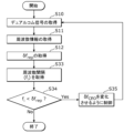
- FIG. 6 is a flowchart showing the process of controlling ⁇ f CEO based on the lowest frequency mode in the frequency spectrum of the dual comb signal, among the operations of laser device 100 according to the present embodiment.
- FIG. 6 is to control so that X in FIG. 4 does not take a negative value. If X becomes a negative value, as shown in FIG. 7, the frequency spectrum will fold back around the zero value due to aliasing, making it impossible to properly detect the dual comb signal. Note that FIG. 7 is a diagram showing an example of an inappropriate frequency spectrum of a dual comb signal.
- Step S10 the signal processing circuit 80 acquires a dual comb signal detected by at least one of the detectors 71 and 72.
- the dual comb signal obtained here is time information of a pulse train as shown in FIG. Next, the process advances to step S11.
- Step S11 the signal processing circuit 80 acquires frequency information by converting the acquired time information.
- the frequency information acquired here is a frequency spectrum of interference light, for example, a frequency spectrum as shown in FIG. 4.
- the signal processing circuit 80 performs fast Fourier transform as an example of calculations used for conversion, but other methods may be used as long as time information can be converted into frequency information.
- the signal processing circuit 80 outputs the acquired frequency information to the control circuit 90.
- the process advances to step S12.
- Step S12 the control circuit 90 obtains ⁇ f rep , which is the difference in repetition frequency.
- ⁇ f rep the repetition frequency
- the control circuit 90 controls the repetition frequency f rep1 of the first optical comb laser 10 and the repetition frequency f rep2 of the second optical comb laser 20
- An example of controlling the repetition frequency is to control the cavity length of each of the first optical comb laser 10 and the second optical comb laser 20 by feedback control, but if the repetition frequency can be controlled, other It doesn't matter what method you use. Further, as long as information on ⁇ f rep can be obtained, a method other than the above may be used.
- the process advances to step S13.
- step S13 the control circuit 90 obtains first information regarding the lowest frequency mode of the frequency spectrum obtained in step S12. Specifically, the first information is the mode frequency f min of the lowest frequency mode. As an example, the control circuit 90 can detect f min by performing peak detection in the frequency spectrum, but other methods may be used as long as f min can be detected. Next, the process advances to step S14.
- step S14 the control circuit 90 determines whether f min is smaller than ⁇ f rep . In step S14, if f min is smaller than ⁇ f rep , that is, if Yes in step S14, the process advances to step S15. On the other hand, if f min is greater than or equal to ⁇ f rep in step S14, that is, if No in step S14, the control of ⁇ f CEO based on the lowest frequency mode ends. If No in step S14, ⁇ f CEO does not need to be changed.
- step S15 the control circuit 90 changes ⁇ f CEO by controlling at least one of f CEO1 of the first optical comb laser 10 and f CEO2 of the second optical comb laser 20.
- the control circuit 90 changes at least one of f CEO1 and f CEO2 by adjusting the output of the excitation source of the first optical comb laser 10 or the second optical comb laser 20, but does not change the value of f CEO1 or f CEO2 . If it can be changed, other methods such as control using an AOM (Acoustic Optic Modulator) may be used.
- AOM Acoustic Optic Modulator
- FIG. 7 shows an example where X shown in FIG. 4 takes a negative value and aliasing occurs.
- Two frequency modes represented by broken lines
- the lowest frequency mode is the third frequency mode from the left when no aliasing occurs, as shown in FIG.
- the control circuit 90 increases ⁇ f CEO by changing the value of f CEO1 or f CEO2 .
- the amount by which ⁇ f CEO is increased is adjusted as appropriate. Note that if ⁇ f CEO is made too large, a problem arises in that it exceeds the response frequency band. How to deal with this problem will be explained in detail later using FIGS. 8 and 9.
- the signal processing circuit 80 may acquire the dual comb signal detected by each of the detectors 71 and 72.
- the dual comb signals detected by each of detectors 71 and 72 are required.
- the position of the frequency spectrum may shift slightly due to the Doppler effect of light.
- the dual comb signals of each of the detectors 71 and 72 are acquired, and the processes of steps S11 to S15 are executed for each. Good too. The same applies to FIGS. 8, 10, and 12.
- FIG. 8 is a flowchart showing the process of controlling ⁇ f CEO based on the highest frequency mode in the frequency spectrum of the dual comb signal, among the operations of laser device 100 according to the present embodiment.
- FIG. 8 The process shown in FIG. 8 is to control the frequency spectrum so that it does not exceed the maximum value F max of the response frequency bands of the detectors 71 and 72 in FIG. 4 . If the frequency spectrum exceeds the maximum value F max of the response frequency bands of the detectors 71 and 72, the frequency spectrum will be aliased around F max due to aliasing, as shown in FIG. The signal cannot be detected properly.
- FIG. 9 is a diagram showing an example of an inappropriate frequency spectrum of a dual comb signal.
- the laser device 100 starts operating in response to a start signal from an input means (not shown). Steps S10, S11, and S12 are the same as the processing shown in FIG. 6, so their explanation will be omitted.
- step S23 the control circuit 90 obtains second information regarding the highest frequency mode of the frequency spectrum obtained in step S11.
- the second information is the mode frequency f max of the highest frequency mode.
- the control circuit 90 can detect f max by performing peak detection in the frequency spectrum, but other methods may be used as long as f max can be detected.
- the process advances to step S24.
- step S24 the control circuit 90 determines whether f max is greater than F max ⁇ f rep . In step S24, if f max is larger than F max ⁇ f rep , that is, if Yes in step S24, the process advances to step S25. On the other hand, if f max is less than or equal to F max ⁇ f rep in step S24, that is, if No in step S24, the control of ⁇ f CEO based on the highest frequency mode ends.
- step S25 the control circuit 90 changes ⁇ f CEO by controlling at least one of f CEO1 of the first optical comb laser 10 and f CEO2 of the second optical comb laser 20.
- the control circuit 90 changes at least one of f CEO1 and f CEO2 by adjusting the output of the excitation source of the first optical comb laser 10 or the second optical comb laser 20, but does not change the value of f CEO1 or f CEO2 . If it can be changed, other methods such as control using an AOM may be used.
- the process returns to step S10 and the above process is repeated. If No in step S24, ⁇ f CEO does not need to be changed.
- FIG. 9 shows an example in which aliasing occurs when the frequency spectrum exceeds the maximum value F max of the response frequency band.
- Five frequency modes represented by broken lines
- the highest frequency mode is the sixth frequency mode from the right when aliasing does not occur, as shown in FIG.
- the control circuit 90 reduces ⁇ f CEO by changing the value of f CEO1 or f CEO2 .
- the amount by which ⁇ f CEO is reduced is adjusted as appropriate. Note that if ⁇ f CEO is made too small, a problem arises in that X takes a negative value.
- the response to this problem is as described using FIGS. 6 and 7.
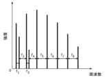
- FIG. 10 is a flowchart showing the process of controlling ⁇ f CEO based on the frequency interval in the frequency spectrum of the dual comb signal, among the operations of laser device 100 according to the present embodiment.
- the process shown in FIG. 10 is for controlling so that aliasing does not occur. If the frequency spectrum is folded back due to aliasing, the fact that a frequency interval smaller than ⁇ f rep occurs in the frequency spectrum is utilized, as shown in FIG.
- frequency intervals between adjacent frequency modes are represented by f 1 to f 8 . Due to the occurrence of aliasing, f 1 , f 2 , f 3 , and f 4 all become smaller than ⁇ f rep (Yes in step S34), so the control circuit 90 changes the value of f CEO1 or f CEO2 . This changes ⁇ f CEO . The amount by which ⁇ f CEO is changed is adjusted as appropriate.
- Step S43 the control circuit 90 acquires one of the lowest frequency mode mode frequency f min , the highest frequency mode mode frequency f max , and frequency interval f i for the frequency spectrum acquired in step S11.
- the control circuit 90 can detect f min , f max and f i by performing peak detection in the frequency spectrum, but if it can detect f min , f max and f i , other It doesn't matter what method you use.
- step S14 if f min is detected, the process proceeds to step S14, if f max is detected, the process proceeds to step S24, and if f i is detected, the process proceeds to step S34.
- the processing in each step S14, S24, and S34 is the same as the processing shown in FIGS. 6, 8, and 10. The same applies to steps S15, S25, and S35.
- the laser device 100 starts operating in response to a start signal from an input means (not shown).
- step S53 the control circuit 90 determines whether the accuracy ⁇ i calculated in step S52 is greater than the previous accuracy ⁇ i ⁇ 1 .
- the smaller the value of precision ⁇ i the better the precision, that is, the smaller the error between the distance measurement result and the actual distance.
- step S53 if ⁇ i is greater than ⁇ i ⁇ 1 , that is, if Yes in step S53, the process advances to step S54.
- step S53 if ⁇ i is smaller than ⁇ i ⁇ 1 in step S53, that is, if No in step S53, the control of ⁇ f CEO based on the accuracy of the distance ends. If No in step S53, ⁇ f CEO does not need to be changed.
- FIG. 14 is a flowchart illustrating an example of a process for controlling ⁇ f CEO as a calibration before measurement among the operations of the laser device 100 according to the present embodiment.
- Step S62 it is determined whether to end distance measurement. Specifically, the signal processing circuit 80 or the control circuit 90 determines whether an end signal is input from an input means (not shown). If the measurement is to be completed in step S62, that is, in the case of Yes in step S62, the distance measurement is completed. On the other hand, if the measurement is to be continued in step S62, that is, if No in step S62, the process advances to step S61.
- FIG. 15 is a flowchart illustrating an example of the process of controlling ⁇ f CEO as feedback during measurement among the operations of laser device 100 according to the present embodiment.
- the processing executed by a specific processing unit may be executed by another processing unit.
- the order of the plurality of processes may be changed, or the plurality of processes may be executed in parallel.
- the processing described in the above embodiments may be realized by performing centralized processing using a single device (system), or by performing distributed processing using multiple devices. It's okay.
- the number of processors that execute the above program may be a single processor or a plurality of processors. That is, centralized processing or distributed processing may be performed.
- all or part of the components such as the signal processing circuit 80 and the control circuit 90 may be configured with dedicated hardware, or a software program suitable for each component may be executed. It may be realized by doing.
- Each component may be realized by a program execution unit such as a CPU (Central Processing Unit) or a processor reading and executing a software program recorded on a recording medium such as an HDD (Hard Disk Drive) or semiconductor memory. good.
- a program execution unit such as a CPU (Central Processing Unit) or a processor reading and executing a software program recorded on a recording medium such as an HDD (Hard Disk Drive) or semiconductor memory. good.
- components such as the signal processing circuit 80 and the control circuit 90 may be composed of one or more electronic circuits.
- Each of the one or more electronic circuits may be a general-purpose circuit or a dedicated circuit.
- the one or more electronic circuits may include, for example, a semiconductor device, an IC, or an LSI.
- An IC or LSI may be integrated into one chip or into multiple chips. Here, it is called an IC or an LSI, but the name changes depending on the degree of integration, and may be called a system LSI, VLSI (Very Large Scale Integration), or ULSI (Very Large Scale Integration).
- an FPGA that is programmed after the LSI is manufactured can also be used for the same purpose.
- general or specific aspects of the present disclosure may be implemented in a system, apparatus, method, integrated circuit, or computer program.
- the computer program may be implemented in a computer-readable non-transitory recording medium such as an optical disk, HDD, or semiconductor memory.
- the present invention may be realized by any combination of a system, an apparatus, a method, an integrated circuit, a computer program, and a recording medium.
- FIG. 16 is a diagram showing the processing flow of this modification.
- the laser device is: a first optical comb laser; a second optical comb laser; a detection section; comprising a control circuit;
- the control circuit causes the first optical comb laser to output light (1,p) in a p-th period
- the control circuit causes the second optical comb laser to output light (2, p) in a p-th period
- the detection unit receives light (3,p) based on the light (1,p) and the light (2,p),
- the f 1, n, p is the optical frequency of the n-th mode shown in the frequency spectrum characteristic (1, p) of the light (1, p)
- the f2 ,n,p is the optical frequency of the n-th mode shown in the frequency spectrum characteristic (2,p) of
- the light (1, p) may be a laser light output by the first optical comb laser 10 in the p-th period.
- the light (2, p) may be a laser light output by the second optical comb laser 20 in the p-th period.
- the light (3,p) may be light based on the light (1,p) and the light (2,p), and may be light that the detector 32 receives from the coupler 32.
- the pth period may start at time t p and end at time t (p+1) .
- the control circuit may cause the first optical comb laser to stop outputting the light (1,p) at a time that is after the time t p and before the time t (p+1 ). good.
- the control circuit may cause the second optical comb laser to stop outputting the light (2,p) at a time that is after the time t p and before the time t (p+1). good.
- the time at which the output of the light (2,p) ends may be after the time t p and before the time t (p+1) .
- the laser device according to the second item is the laser device according to the first item, the frequency spectrum characteristic (3, p) indicates f min ⁇ f rep ;
- the f min is a wavelength corresponding to the lowest frequency mode among the plurality of frequency modes shown in the frequency spectrum characteristic (3,p)
- the ⁇ f rep is the absolute value of the difference between two frequencies corresponding to two adjacent frequency modes in the frequency spectrum characteristic (3,p).
- the laser device is the laser device according to the first item, the frequency spectrum characteristic (3,p) indicates f max >(F max - ⁇ f rep );
- the f max is a wavelength corresponding to the highest frequency mode among the plurality of frequency modes shown in the frequency spectrum characteristic (3, p),
- the F max is the largest frequency included in a frequency band detectable by the detection unit,
- the ⁇ f rep is the absolute value of the difference between two frequencies corresponding to two adjacent frequency modes in the frequency spectrum characteristic (3,p).
- the present disclosure can be used in devices, systems, or methods that perform distance measurement or displacement measurement, and can be used, for example, in distance measurement sensors, displacement meters, shape inspection devices, and the like.
Abstract
A laser device (100) comprises: a first optical comb laser (10); a second optical comb laser (20) having a different repetition frequency from the first optical comb laser (10); a detection unit (70) that detects interference light between the output light from the first optical comb laser (10) and the output light from the second optical comb laser (20); and a control circuit (90). The control circuit (90) controls at least one of a first CEO frequency that is a carrier envelope offset frequency of the first optical comb laser (10) or a second CEO frequency that is a carrier envelope offset frequency of the second optical comb laser (20) on the basis of the output of the detection unit (70), thereby changing a difference frequency that is the difference between the first CEO frequency and the second CEO frequency.
Description
本開示は、レーザ装置に関する。
The present disclosure relates to a laser device.
従来、光周波数コムレーザまたは単に光コムレーザと称されるレーザ光源が知られている。具体的には、光周波数コムレーザは、時間軸上ではパルス波形が等間隔に並び、かつ、周波数軸上ではスペクトルが等間隔に並んだレーザ光を出力する光源である。
Conventionally, a laser light source called an optical frequency comb laser or simply an optical comb laser is known. Specifically, an optical frequency comb laser is a light source that outputs laser light in which pulse waveforms are arranged at equal intervals on the time axis and spectra are arranged at equal intervals on the frequency axis.
特許文献1には、2つの発振器のキャリアエンベロープオフセット周波数(fCEO)の差を安定させるように制御するコヒーレントデュアル走査レーザシステムが開示されている。また、特許文献2には、2つの発振器のキャリアエンベロープオフセット周波数(fCEO)の差が繰り返し周波数(frep)の整数倍になるように制御する光コムの制御方法が開示されている。
Patent Document 1 discloses a coherent dual scanning laser system that is controlled to stabilize the difference in carrier envelope offset frequency (f CEO ) between two oscillators. Further, Patent Document 2 discloses an optical comb control method in which the difference between the carrier envelope offset frequencies (f CEO ) of two oscillators is controlled to be an integral multiple of the repetition frequency (f rep ).
しかしながら、上記従来技術のように、キャリアエンベロープオフセット周波数の差を安定にするだけでは、出力される光を検出器で精度良く検出することができない場合がある。
However, as in the above-mentioned conventional technology, it may not be possible to accurately detect the output light with a detector simply by stabilizing the difference in carrier envelope offset frequency.
本開示は、検出器で精度良く検出することができる光を出力するレーザ装置を提供する。
The present disclosure provides a laser device that outputs light that can be detected with high accuracy by a detector.
本開示の一態様に係るレーザ装置は、第1光コムレーザと、前記第1光コムレーザとは繰り返し周波数が異なる第2光コムレーザと、前記第1光コムレーザからの出力光と前記第2光コムレーザからの出力光とによる干渉光を検出する検出部と、制御回路と、を備え、前記制御回路は、前記第1光コムレーザのキャリアエンベロープオフセット周波数である第1CEO周波数と、前記第2光コムレーザのキャリアエンベロープオフセット周波数である第2CEO周波数との少なくとも一方を、前記検出部の出力に基づいて制御することで、前記第1CEO周波数と前記第2CEO周波数との差である差分周波数を変化させる。
A laser device according to an aspect of the present disclosure includes a first optical comb laser, a second optical comb laser having a repetition frequency different from that of the first optical comb laser, and an output light from the first optical comb laser and an output light from the second optical comb laser. and a control circuit, the control circuit detecting a first CEO frequency, which is a carrier envelope offset frequency of the first optical comb laser, and a carrier envelope offset frequency of the second optical comb laser. By controlling at least one of the second CEO frequency, which is the envelope offset frequency, based on the output of the detection section, a difference frequency, which is the difference between the first CEO frequency and the second CEO frequency, is changed.
本開示によれば、検出器で精度良く検出することができる光を出力するレーザ装置を提供することができる。
According to the present disclosure, it is possible to provide a laser device that outputs light that can be accurately detected by a detector.
(本開示の概要)
光コムレーザでは、2つのパラメータが重要である。1つはスペクトル間隔を表す「繰り返し周波数」(frep)である。もう1つはスペクトルを0まで外挿していった際の余りを表す「キャリアエンベロープオフセット周波数」(fCEO)である。これらのパラメータは、振動および温度などの外乱によって僅かに変化してしまう。これに対して、ペルチェ素子またはピエゾ素子などの変調機器を光コムレーザに組み込むことで、これらのパラメータを安定化させることができる。これにより、精密測定を実現することができる。 (Summary of this disclosure)
Two parameters are important in optical comb lasers. One is the "repetition frequency" (f rep ), which represents the spectral interval. The other is the "carrier envelope offset frequency" (f CEO ), which represents the remainder when the spectrum is extrapolated to 0. These parameters change slightly due to disturbances such as vibration and temperature. On the other hand, these parameters can be stabilized by incorporating a modulation device such as a Peltier element or a piezo element into the optical comb laser. Thereby, precise measurement can be achieved.
この光コムレーザを2つ用意し、それぞれの繰り返し周波数を僅かにずらしたものを干渉させて計測する手法をデュアルコムと呼ぶ。デュアルコムでは、繰り返し周波数がそれぞれfrep、frep+δfrepである2つの光コムレーザが干渉することで、ビート(うなり)が発生する。結果として、間隔がδfrepのスペクトルを取得することができる。ここで重要なのは、干渉前の光コムレーザのスペクトルは、光の周波数であるTHz領域である一方で、干渉後のスペクトルはラジオ周波数のMHz領域になることである。
Dual comb is a method in which two optical comb lasers are prepared, and their repetition frequencies are slightly shifted, allowing them to interfere with each other for measurement. In a dual comb, two optical comb lasers whose repetition frequencies are f rep and f rep +δf rep , respectively, interfere with each other, thereby generating a beat. As a result, spectra with intervals of δf rep can be obtained. What is important here is that the spectrum of the optical comb laser before interference is in the THz region, which is the frequency of light, while the spectrum after interference is in the MHz region, which is the radio frequency.
従来の検出器は、応答周波数がGHz以下のため、物理的にTHz領域の光の信号を検出できない。そのため、従来では光の波長を調べる際には直接に検出器を用いることができず、代わりに分光器を使って光を波長毎に分けた後に検出器を用いて検出する。この場合、波長の掃引に時間がかかってしまい短期間にスペクトルの測定をすることができないという欠点がある。
Since the response frequency of conventional detectors is below GHz, they cannot physically detect optical signals in the THz region. Therefore, conventionally, when investigating the wavelength of light, it is not possible to directly use a detector; instead, a spectroscope is used to separate the light into wavelengths, and then a detector is used to detect the wavelength. In this case, there is a drawback that it takes time to sweep the wavelength, making it impossible to measure the spectrum in a short period of time.
これに対して、デュアルコムの場合、光をMHz領域にダウンコンバージョンすることができるので分光器を介す必要がない。このため、従来に比べて、高速にスペクトルの測定ができるという長所がある。加えて、光の情報を直接測定できることから、高感度かつ高精度の測定を実現できる。これにより、分光測定、距離測定、周波数測定など多種多様な測定においてデュアルコムが用いられるようになっている。
On the other hand, in the case of a dual comb, the light can be down-converted to the MHz region, so there is no need to pass it through a spectrometer. Therefore, it has the advantage that spectra can be measured faster than conventional methods. In addition, since optical information can be directly measured, highly sensitive and highly accurate measurements can be achieved. As a result, dual combs have come to be used in a wide variety of measurements such as spectroscopic measurements, distance measurements, and frequency measurements.
しかしながら、デュアルコムを利用する場合であっても、応答周波数帯域が狭い安価な検出器を用いた場合、2つの光コムレーザのキャリアエンベロープオフセット周波数fCEOの差であるδfCEOの値によっては、応答周波数帯域を越えてしまい、測定が困難になるケースがある。
However, even when using a dual comb, if an inexpensive detector with a narrow response frequency band is used, the response may vary depending on the value of δf CEO , which is the difference between the carrier envelope offset frequencies f CEO of the two optical comb lasers. There are cases where the frequency band is exceeded, making measurement difficult.
本開示の一態様に係るレーザ装置は、第1光コムレーザと、前記第1光コムレーザとは繰り返し周波数が異なる第2光コムレーザと、前記第1光コムレーザからの出力光と前記第2光コムレーザからの出力光とによる干渉光を検出する検出部と、制御回路と、を備え、前記制御回路は、前記第1光コムレーザのキャリアエンベロープオフセット周波数である第1CEO周波数と、前記第2光コムレーザのキャリアエンベロープオフセット周波数である第2CEO周波数との少なくとも一方を、前記検出部の出力に基づいて制御することで、前記第1CEO周波数と前記第2CEO周波数との差である差分周波数を変化させる。
A laser device according to an aspect of the present disclosure includes a first optical comb laser, a second optical comb laser having a repetition frequency different from that of the first optical comb laser, and an output light from the first optical comb laser and an output light from the second optical comb laser. and a control circuit, the control circuit detecting a first CEO frequency, which is a carrier envelope offset frequency of the first optical comb laser, and a carrier envelope offset frequency of the second optical comb laser. By controlling at least one of the second CEO frequency, which is the envelope offset frequency, based on the output of the detection section, a difference frequency, which is the difference between the first CEO frequency and the second CEO frequency, is changed.
これにより、干渉光を検出する検出部の出力を利用することで、差分周波数(δfCEO)が検出部の応答周波数帯域内に入るように調整することができる。したがって、応答周波数帯域が狭い検出器を利用した場合でも、精度良く検出することができる。
Thereby, by using the output of the detection section that detects interference light, it is possible to adjust the difference frequency (δf CEO ) to fall within the response frequency band of the detection section. Therefore, even when a detector with a narrow response frequency band is used, accurate detection is possible.
また、本開示の一態様に係るレーザ装置では、例えば、前記制御回路は、前記検出部の出力に基づいて前記干渉光の周波数スペクトルの最も低い周波数モードに関する第1情報を取得し、取得した第1情報を用いて、前記差分周波数を大きくしてもよい。
Further, in the laser device according to one aspect of the present disclosure, for example, the control circuit acquires first information regarding the lowest frequency mode of the frequency spectrum of the interference light based on the output of the detection unit, and 1 information may be used to increase the difference frequency.
これにより、最も低い周波数モードが応答周波数帯域内の適切な範囲に検出されるようにすることができる。このため、エイリアシングなどの発生により、検出精度の低下を抑制することができる。
This allows the lowest frequency mode to be detected in an appropriate range within the response frequency band. Therefore, it is possible to suppress a decrease in detection accuracy due to occurrence of aliasing or the like.
また、本開示の一態様に係るレーザ装置では、例えば、前記制御回路は、前記検出部の出力に基づいて前記干渉光の周波数スペクトルの最も高い周波数モードに関する第2情報を取得し、取得した第2情報を用いて、前記差分周波数を小さくしてもよい。
Further, in the laser device according to one aspect of the present disclosure, for example, the control circuit acquires second information regarding the highest frequency mode of the frequency spectrum of the interference light based on the output of the detection unit, and 2 information may be used to reduce the difference frequency.
これにより、最も高い周波数モードが応答周波数帯域内の適切な範囲に検出されるようにすることができる。このため、エイリアシングなどの発生により、検出精度の低下を抑制することができる。
This allows the highest frequency mode to be detected in an appropriate range within the response frequency band. Therefore, it is possible to suppress a decrease in detection accuracy due to occurrence of aliasing or the like.
また、本開示の一態様に係るレーザ装置では、例えば、前記制御回路は、前記検出部の出力に基づいて前記干渉光の周波数スペクトルの周波数間隔に関する第3情報を取得し、取得した第3情報を用いて、前記差分周波数を変化させてもよい。
Further, in the laser device according to one aspect of the present disclosure, for example, the control circuit acquires third information regarding a frequency interval of the frequency spectrum of the interference light based on the output of the detection unit, and the acquired third information The difference frequency may be changed using .
これにより、エイリアシングの発生の有無を検出できる。このため、エイリアシングが発生している場合には、干渉光の周波数スペクトルを応答周波数帯域内に収まるようにすることができ、検出精度の低下を抑制することができる。
With this, it is possible to detect whether aliasing has occurred. Therefore, when aliasing occurs, the frequency spectrum of the interference light can be made to fall within the response frequency band, and a decrease in detection accuracy can be suppressed.
また、本開示の一態様に係るレーザ装置では、例えば、前記検出部は、前記第1光コムレーザからの出力光の、対象物による反射光と、前記第2光コムレーザからの出力光との干渉光を検出し、前記レーザ装置は、前記検出部の出力に基づいて前記対象物までの距離を算出する信号処理回路を備えてもよい。
Further, in the laser device according to one aspect of the present disclosure, for example, the detection unit may detect interference between reflected light from an object of output light from the first optical comb laser and output light from the second optical comb laser. The laser device may include a signal processing circuit that detects light and calculates a distance to the object based on the output of the detection section.
これにより、対象物に対する測距および形状の検査などを精度良く行うことができる。
Thereby, distance measurement and shape inspection of the target object can be performed with high accuracy.
また、本開示の一態様に係るレーザ装置では、例えば、前記制御回路は、前記信号処理回路が算出した距離の精度に基づいて前記差分周波数を変化させてもよい。
Furthermore, in the laser device according to one aspect of the present disclosure, for example, the control circuit may change the differential frequency based on the accuracy of the distance calculated by the signal processing circuit.
これにより、距離の精度を高めることができる。
Thereby, the accuracy of distance can be improved.
また、本開示の一態様に係るレーザ装置では、例えば、前記制御回路は、前記距離の算出を行う前に前記差分周波数を変化させてもよい。
Furthermore, in the laser device according to one aspect of the present disclosure, for example, the control circuit may change the differential frequency before calculating the distance.
これにより、差分周波数(δfCEO)のキャリブレーションが可能になるので、測定時には最初から精度良く測定が可能になる。
This makes it possible to calibrate the differential frequency (δf CEO ), making it possible to measure accurately from the beginning.
また、本開示の一態様に係るレーザ装置では、例えば、前記制御回路は、前記距離の算出を行いながら前記差分周波数を変化させしてもよい。
Furthermore, in the laser device according to one aspect of the present disclosure, for example, the control circuit may change the differential frequency while calculating the distance.
これにより、差分周波数(δfCEO)のフィードバックが可能になるので、測定しながら精度を高めることができる。なお、「距離の算出を行いながら」とは、距離の算出と差分周波数の変化とを実質的に同時並行的に行うことを意味する。例えば、「距離の算出を行いながら」は、距離の算出と差分周波数の変化とを完全に同時に行う場合だけでなく、それぞれを交互に繰り返し行う場合も意味する。交互の繰り返しは、1回ずつ交互に繰り返してもよく、一方の処理を複数回行った場合に、他方の処理を1回行う場合も含んでいる。
This enables feedback of the difference frequency (δf CEO ), so accuracy can be improved while measuring. Note that "while calculating the distance" means calculating the distance and changing the difference frequency substantially simultaneously. For example, "while calculating the distance" means not only the case where the calculation of the distance and the change of the difference frequency are performed completely simultaneously, but also the case where they are repeatedly performed alternately. The alternating repetition may be repeated one time at a time, and also includes a case where one process is performed multiple times and the other process is performed once.
また、本開示の一態様に係るレーザ装置は、上述した各態様に係るレーザ装置の構成要素を適宜組み合わせて構成されてもよい。
Further, the laser device according to one aspect of the present disclosure may be configured by appropriately combining the constituent elements of the laser device according to each aspect described above.
以下では、実施の形態について、図面を参照しながら具体的に説明する。
Hereinafter, embodiments will be specifically described with reference to the drawings.
なお、以下で説明する実施の形態は、いずれも包括的または具体的な例を示すものである。以下の実施の形態で示される数値、形状、材料、構成要素、構成要素の配置位置および接続形態、ステップ、ステップの順序などは、一例であり、本開示を限定する主旨ではない。また、以下の実施の形態における構成要素のうち、独立請求項に記載されていない構成要素については、任意の構成要素として説明される。
Note that the embodiments described below are comprehensive or specific examples. The numerical values, shapes, materials, components, arrangement positions and connection forms of the components, steps, order of steps, etc. shown in the following embodiments are examples, and do not limit the present disclosure. Further, among the constituent elements in the following embodiments, constituent elements that are not described in the independent claims will be described as arbitrary constituent elements.
また、各図は、模式図であり、必ずしも厳密に図示されたものではない。したがって、例えば、各図において縮尺などは必ずしも一致しない。また、各図において、実質的に同一の構成については同一の符号を付しており、重複する説明は省略または簡略化する。
Furthermore, each figure is a schematic diagram and is not necessarily strictly illustrated. Therefore, for example, the scales and the like in each figure do not necessarily match. Further, in each figure, substantially the same configurations are denoted by the same reference numerals, and overlapping explanations will be omitted or simplified.
また、本明細書において、「第1」、「第2」などの序数詞は、特に断りの無い限り、構成要素の数または順序を意味するものではなく、同種の構成要素の混同を避け、区別する目的で用いられている。
In addition, in this specification, ordinal numbers such as "first" and "second" do not mean the number or order of components, unless otherwise specified, and do not mean the number or order of components. It is used for the purpose of
(実施の形態)
[光コムレーザ]
まず、図1および図2を参照して、光コムレーザの基本原理を簡単に説明する。 (Embodiment)
[Optical comb laser]
First, the basic principle of an optical comb laser will be briefly explained with reference to FIGS. 1 and 2.
[光コムレーザ]
まず、図1および図2を参照して、光コムレーザの基本原理を簡単に説明する。 (Embodiment)
[Optical comb laser]
First, the basic principle of an optical comb laser will be briefly explained with reference to FIGS. 1 and 2.
図1は、光コムレーザ光の電界の時間変化の例を模式的に示す図である。図1において、横軸は時間を表し、縦軸は光コムレーザ光の電界を表している。なお、光コムレーザ光は、光周波数コムレーザ光とも呼ばれる。また、本明細書では、単にレーザ光と記載する場合もある。
FIG. 1 is a diagram schematically showing an example of a temporal change in the electric field of an optical comb laser beam. In FIG. 1, the horizontal axis represents time, and the vertical axis represents the electric field of the optical comb laser beam. Note that the optical comb laser beam is also called an optical frequency comb laser beam. Further, in this specification, it may be simply referred to as laser light.
図1に示すように、光コムレーザ光は、繰り返し周期Trepで発生する光パルス列から形成されている。繰り返し周期Trepは、例えば1ps以上100ns以下である。各光パルスの半値全幅はΔtによって表される。各光パルスの半値全幅Δtは、例えば10fs以上100ps以下である。
As shown in FIG. 1, the optical comb laser beam is formed from a train of optical pulses generated at a repeating period T rep . The repetition period T rep is, for example, 1 ps or more and 100 ns or less. The full width at half maximum of each optical pulse is represented by Δt. The full width at half maximum Δt of each optical pulse is, for example, 10 fs or more and 100 ps or less.
レーザ共振器では、光パルスの包絡線が伝搬する群速度vgと、光パルス内の波が伝搬する位相速度vpとが、共振器内の分散などにより異なる値をとる。群速度vgと位相速度vpとの違いに起因して、隣接する2つの光パルスを包絡線が一致するように重ねると、これらの光パルス内の波の位相はΔφだけシフトする。Δφは0から2πの間の値をとる。つまり、0≦Δφ≦2πである。光パルス列の繰り返し周期は、レーザ共振器の周回長(round-trip length)をLとして、Trep=L/vgによって表される。
In a laser resonator, the group velocity v g at which the envelope of the optical pulse propagates and the phase velocity v p at which the wave within the optical pulse propagates take different values due to dispersion within the resonator and the like. Due to the difference in group velocity v g and phase velocity v p , when two adjacent light pulses are superimposed with matching envelopes, the phase of the waves in these light pulses is shifted by Δφ. Δφ takes a value between 0 and 2π. That is, 0≦Δφ≦2π. The repetition period of the optical pulse train is expressed by T rep =L/v g , where L is the round-trip length of the laser resonator.
図2は、光コムレーザ光の周波数スペクトルを模式的に示す図である。図2において、横軸は周波数を表し、縦軸は光コムレーザ光の強度を表している。
FIG. 2 is a diagram schematically showing the frequency spectrum of optical comb laser light. In FIG. 2, the horizontal axis represents the frequency, and the vertical axis represents the intensity of the optical comb laser beam.
図2に示すように、光コムレーザ光は、複数の離散的な等間隔線から形成された櫛状の周波数スペクトルを有する。複数の離散的な等間隔線の周波数は、レーザ共振器における縦モードの共振周波数に相当する。光コムレーザ光における隣接する2つの等間隔線の間隔に相当する繰り返し周波数は、frep=1/Trepによって表される。繰り返し周波数frepは、例えば10MHz以上1THz以下である。レーザ共振器の周回長Lは30cmであり、かつ、群速度vgが真空中の光速(=3×108m/s)にほぼ等しい場合、繰り返し周期Trepは1nsになり、繰り返し周波数frepは1GHzになる。
As shown in FIG. 2, the optical comb laser beam has a comb-shaped frequency spectrum formed from a plurality of discrete equally spaced lines. The frequencies of the plurality of discrete equally spaced lines correspond to the resonance frequency of the longitudinal mode in the laser resonator. The repetition frequency corresponding to the interval between two adjacent equally spaced lines in the optical comb laser beam is expressed by f rep =1/T rep . The repetition frequency f rep is, for example, 10 MHz or more and 1 THz or less. If the circumferential length L of the laser resonator is 30 cm and the group velocity v g is approximately equal to the speed of light in vacuum (=3×10 8 m/s), the repetition period T rep will be 1 ns, and the repetition frequency f rep will be 1GHz.
光コムレーザ光の半値全幅をΔfとした場合、Δf=1/Δtである。光コムレーザ光の半値全幅Δfは、例えば10GHz以上100THz以下である。等間隔線がゼロ周波数付近まで存在すると仮定した場合における、ゼロ周波数に最も近い等間隔線の周波数は、キャリアエンベロープオフセット周波数と呼ばれる。キャリアエンベロープオフセット周波数は、fCEO=(Δφ/(2π))frepによって表される。キャリアエンベロープオフセット周波数fCEOは、0から繰り返し周波数frepの間の値をとる。つまり、0≦fCEO≦frepである。キャリアエンベロープオフセット周波数fCEOを0番目のモード周波数とすると、光コムレーザ光におけるn番目のモード周波数fnは、fn=fCEO+nfrepによって表される。図1に示す光コムレーザ光の電界は、n番目のモード周波数fnでの電界の振幅および位相をそれぞれEnおよびφnとして、E(t)=ΣnEnexp[-i(2πfnt+φn)]によって表される。
When the full width at half maximum of the optical comb laser beam is Δf, Δf=1/Δt. The full width at half maximum Δf of the optical comb laser beam is, for example, 10 GHz or more and 100 THz or less. Assuming that the equally spaced lines exist up to the vicinity of the zero frequency, the frequency of the equally spaced line closest to the zero frequency is called the carrier envelope offset frequency. The carrier envelope offset frequency is represented by f CEO = (Δφ/(2π))f rep . The carrier envelope offset frequency f CEO takes a value between 0 and the repetition frequency f rep . That is, 0≦f CEO ≦f rep . If the carrier envelope offset frequency f CEO is the 0th mode frequency, the nth mode frequency f n in the optical comb laser beam is expressed by f n = f CEO + nf rep . The electric field of the optical comb laser beam shown in FIG. 1 is expressed as E( t ) =ΣnE n exp[−i(2πf n t+ φ n )].
繰り返し周波数frepおよびキャリアエンベロープオフセット周波数fCEOは、光コムレーザ光源に対する振動または温度変化などの外乱によって僅かに変化し得る。これは、振動がレーザ共振器の周回長Lを変化させ、また、温度変化がレーザ共振器の屈折率変化を介して群速度vgおよび位相速度vpを変化させ得るからである。繰り返し周波数frepおよびキャリアエンベロープオフセット周波数fCEOは、光の周波数よりもはるかに低い。それらの僅かな変化でも、光コムレーザ光におけるモード周波数の特定に影響を及ぼし得る。このため、従来の光コムレーザ光源には、繰り返し周波数frepおよびキャリアエンベロープオフセット周波数fCEOを安定化させる変調素子が組み込まれている。
The repetition frequency f rep and the carrier envelope offset frequency f CEO may change slightly due to disturbances such as vibrations or temperature changes to the optical comb laser source. This is because vibrations change the circumferential length L of the laser cavity, and temperature changes can also change the group velocity v g and phase velocity v p via changes in the refractive index of the laser cavity. The repetition frequency f rep and the carrier envelope offset frequency f CEO are much lower than the optical frequency. Even a slight change in them can affect the identification of the mode frequency in the optical comb laser beam. For this reason, a conventional optical comb laser light source incorporates a modulation element that stabilizes the repetition frequency f rep and the carrier envelope offset frequency f CEO .
変調素子は、例えば、ピエゾ素子などの振動を抑制するための圧電素子、および/または、ペルチェ素子などの温度変化を抑制するための温度調整素子を含む。変調素子は、光コムレーザ光源の外部に設けられてもよい。繰り返し周波数frepを安定化するために、光コムレーザ光の一部を検出し、検出した当該一部に基づいて、ピエゾ素子およびペルチェ素子を用いてレーザ共振器の周回長Lが一定になるように、フィードバックが行われる。キャリアエンベロープオフセット周波数fCEOを安定化するために、非線形光学効果を用いて光コムレーザ光の一部を検出し、検出した当該一部に基づいて、レーザ共振器に入力する励起光の強度を調整することによってレーザ共振器内の非線形性が一定になるように、フィードバックが行われる。
The modulation element includes, for example, a piezoelectric element such as a piezo element for suppressing vibration, and/or a temperature adjustment element such as a Peltier element for suppressing temperature change. The modulation element may be provided outside the optical comb laser light source. In order to stabilize the repetition frequency f rep , a part of the optical comb laser beam is detected, and based on the detected part, the circumferential length L of the laser resonator is made constant using a piezo element and a Peltier element. Feedback will be provided. In order to stabilize the carrier envelope offset frequency f CEO , a part of the optical comb laser light is detected using a nonlinear optical effect, and the intensity of the excitation light input to the laser resonator is adjusted based on the detected part. Feedback is performed so that the nonlinearity within the laser resonator becomes constant.
[デュアルコム]
次に、図3および図4を参照して、デュアルコムの原理を簡単に説明する。 [Dual com]
Next, the principle of the dual comb will be briefly explained with reference to FIGS. 3 and 4.
次に、図3および図4を参照して、デュアルコムの原理を簡単に説明する。 [Dual com]
Next, the principle of the dual comb will be briefly explained with reference to FIGS. 3 and 4.
図3は、デュアルコムにおける第1光コムレーザと第2光コムレーザとの周波数スペクトルを示す図である。第1光コムレーザ光では、n番目のモード周波数f1nは、f1n=fCEO1+nfrep1によって表される。また、第2光コムレーザ光では、n番目のモード周波数f2nは、f2n=fCEO2+nfrep2によって表される。fCEO1は、第1CEO周波数の一例であり、第1光コムレーザのキャリアエンベロープオフセット周波数である。fCEO2は、第2CEO周波数の一例であり、第2光コムレーザのキャリアエンベロープオフセット周波数である。frep1は、第1光コムレーザの繰り返し周波数である。frep2は、第2光コムレーザの繰り返し周波数である。frep1およびfrep2は互いに異なり、frep2=frep1+δfrepの関係が成り立つ。δfrepは、frep1よりもはるかに小さい。δfrepは、例えば1Hz以上10MHz以下である。
FIG. 3 is a diagram showing frequency spectra of a first optical comb laser and a second optical comb laser in a dual comb. In the first optical comb laser beam, the n-th mode frequency f 1n is expressed by f 1n = f CEO1 + nf rep1 . Further, in the second optical comb laser beam, the n-th mode frequency f 2n is expressed by f 2n = f CEO2 + nf rep2 . f CEO1 is an example of the first CEO frequency and is the carrier envelope offset frequency of the first optical comb laser. f CEO2 is an example of the second CEO frequency, and is the carrier envelope offset frequency of the second optical comb laser. f rep1 is the repetition frequency of the first optical comb laser. f rep2 is the repetition frequency of the second optical comb laser. f rep1 and f rep2 are different from each other, and the relationship f rep2 = f rep1 + δf rep holds. δf rep is much smaller than f rep1 . δf rep is, for example, 1 Hz or more and 10 MHz or less.
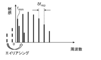
図4は、デュアルコムにおける干渉光の周波数スペクトルを模式的に示す図である。図3における第1光コムレーザと第2光コムレーザとのそれぞれの周波数モードにおいて最近接同士で干渉した結果、図4に示されているような周波数スペクトルが検出される。この干渉光の周波数スペクトルは、デュアルコム信号とも称される。
FIG. 4 is a diagram schematically showing the frequency spectrum of interference light in the dual comb. As a result of interference between the first optical comb laser and the second optical comb laser in their respective frequency modes, the frequency spectra shown in FIG. 4 are detected. The frequency spectrum of this interference light is also called a dual comb signal.
干渉光の周波数スペクトルの周波数間隔は、第1光コムレーザおよび第2光コムレーザの繰り返し周波数の差であるδfrepとなる。図中のXは、0から最も低い周波数モードまでの値を表している。Fmaxは、検出器の応答周波数帯域を表している。図4に示すように干渉光の周波数スペクトルが、Fmaxの中に収まっていればデュアルコム信号の検出が適切であり、測距などの様々な用途に利用することができる。検出器の応答周波数帯域は、検出器が検出可能な周波数帯域であると解釈されてもよい。図4において、δfrepは任意のfiと同じであってもよい。δfrep=(f1+・・・+Fn)/nであってもよい。検出器の応答周波数帯域の最小値は、ゼロであってもよい。検出器の応答周波数帯域の最小値は、ゼロ以外の値であってもよい。
The frequency interval of the frequency spectrum of the interference light is δf rep , which is the difference between the repetition frequencies of the first optical comb laser and the second optical comb laser. X in the figure represents a value from 0 to the lowest frequency mode. F max represents the response frequency band of the detector. As shown in FIG. 4, if the frequency spectrum of the interference light falls within F max , detection of the dual comb signal is appropriate and can be used for various purposes such as ranging. A response frequency band of a detector may be interpreted as a frequency band that is detectable by the detector. In FIG. 4, δf rep may be the same as any fi. δf rep =(f 1 +...+F n )/n. The minimum value of the response frequency band of the detector may be zero. The minimum value of the response frequency band of the detector may be a value other than zero.
ここで、最も低い周波数モードが第1光コムレーザのi番目の周波数モードf1iと第2光コムレーザのj番目の周波数モードf2jとで干渉したものである場合を想定する。この場合、X=f2j-f1i=(fCEO2-fCEO1)+(j-i)frep+jδfrepとなる。
Here, it is assumed that the lowest frequency mode is a result of interference between the i-th frequency mode f 1i of the first optical comb laser and the j-th frequency mode f 2j of the second optical comb laser. In this case, X=f 2j −f 1i =(f CEO2 −f CEO1 )+(ji)f rep +jδf rep .
一例として、frep=3GHz、δfrep=500kHz、i=65000、j=64989と仮定すると、X=(fCEO2-fCEO1)+506MHzになる。ここで、iとjとは光の周波数を195THzとしたときの値である。一方、全モード本数を200本とすると、周波数スペクトルの帯域は100MHz(=δfrep×200)である。
As an example, assuming f rep =3 GHz, δf rep =500 kHz, i=65000, j=64989, then X=(f CEO2 - f CEO1 )+506 MHz. Here, i and j are values when the frequency of light is 195 THz. On the other hand, if the total number of modes is 200, the frequency spectrum band is 100 MHz (=δf rep ×200).
以上より、Fmax≧X+100MHz=δfCEO+606MHzであればきちんと検出することができる。ここで、δfCEOは、第1CEO周波数と第2CEO周波数との差である差分周波数の一例である。具体的には、δfCEO=fCEO2-fCEO1が満たされる。δfCEOがとる値の最高としては約3GHzであることから、場合によっては3.6GHzの応答周波数帯域を有する検出器が必要になる。
From the above, if F max ≧X+100 MHz=δf CEO +606 MHz, it can be properly detected. Here, δf CEO is an example of a difference frequency that is the difference between the first CEO frequency and the second CEO frequency. Specifically, δf CEO =f CEO2 - f CEO1 is satisfied. Since the maximum value of δf CEO is approximately 3 GHz, a detector with a response frequency band of 3.6 GHz may be required in some cases.
一般に、1GHzを超えるような応答周波数帯域が高い検出器は、コストが高くなってしまい、産業応用する際の障壁になるという課題がある。本発明者らは、低い応答周波数帯域を有する安価な検出器でもデュアルコム測定の検出が可能になるように、δfCEOを制御することができるレーザ装置を想到した。
Generally, a detector with a high response frequency band exceeding 1 GHz has a problem of high cost, which becomes a barrier to industrial application. The present inventors conceived of a laser device that can control δf CEO so that dual comb measurements can be detected even with an inexpensive detector having a low response frequency band.
[レーザ装置の構成]
以下、本開示の実施の形態に係るレーザ装置の具体的な構成を説明する。 [Laser device configuration]
Hereinafter, a specific configuration of a laser device according to an embodiment of the present disclosure will be described.
以下、本開示の実施の形態に係るレーザ装置の具体的な構成を説明する。 [Laser device configuration]
Hereinafter, a specific configuration of a laser device according to an embodiment of the present disclosure will be described.
図5は、実施の形態に係るレーザ装置の一例を模式的に示す図である。まず、図5を参照して、本開示の実施の形態に係るレーザ装置100の基本的な構成例を説明する。レーザ装置100は、対象物60までの距離の測定、すなわち、測距を行う。あるいは、レーザ装置100は、対象物60の形状の検査などを行ってもよい。
FIG. 5 is a diagram schematically showing an example of a laser device according to an embodiment. First, with reference to FIG. 5, a basic configuration example of a laser device 100 according to an embodiment of the present disclosure will be described. The laser device 100 measures the distance to the target object 60, that is, performs distance measurement. Alternatively, the laser device 100 may inspect the shape of the object 60.
図5に示すように、レーザ装置100は、第1光コムレーザ10と、第2光コムレーザ20と、検出部70と、信号処理回路80と、制御回路90と、を備える。また、レーザ装置100は、光路を調整する光学素子として、カプラ30、31、32および33と、サーキュレータ40と、コリメータ50と、を備える。
As shown in FIG. 5, the laser device 100 includes a first optical comb laser 10, a second optical comb laser 20, a detection section 70, a signal processing circuit 80, and a control circuit 90. The laser device 100 also includes couplers 30, 31, 32, and 33, a circulator 40, and a collimator 50 as optical elements for adjusting the optical path.
第1光コムレーザ10は、レーザ共振器を含む光コムレーザ光源である。第1光コムレーザ10は、第1光コムレーザ光10Lを出力光として出力する。第1光コムレーザ光10Lは、例えば図3の上段に示すように、繰り返し周波数がfrep1で、キャリアエンベロープオフセット周波数がfCEO1のレーザ光である。
The first optical comb laser 10 is an optical comb laser light source including a laser resonator. The first optical comb laser 10 outputs the first optical comb laser beam 10L as output light. The first optical comb laser beam 10L is a laser beam having a repetition frequency f rep1 and a carrier envelope offset frequency f CEO1 , as shown in the upper part of FIG. 3, for example.
第2光コムレーザ20は、レーザ共振器を含む光コムレーザ光源である。第2光コムレーザ20は、第1光コムレーザ10とは繰り返し周波数が異なる。第2光コムレーザ20は、第2光コムレーザ光20Lを出力光として出力する。第2光コムレーザ光20Lは、例えば図3の下段に示すように、繰り返し周波数がfrep2で、キャリアエンベロープオフセット周波数がfCEO2のレーザ光である。
The second optical comb laser 20 is an optical comb laser light source including a laser resonator. The second optical comb laser 20 has a different repetition frequency from the first optical comb laser 10. The second optical comb laser 20 outputs the second optical comb laser beam 20L as output light. The second optical comb laser beam 20L is a laser beam having a repetition frequency of f rep2 and a carrier envelope offset frequency of f CEO2 , as shown in the lower part of FIG. 3, for example.
カプラ30、31、32および33はそれぞれ、光を分波または結合する光学素子である。
The couplers 30, 31, 32, and 33 are optical elements that separate or combine light, respectively.
サーキュレータ40は、光の進行方向を制御する光学素子である。
The circulator 40 is an optical element that controls the traveling direction of light.
コリメータ50は、光を平行光にして出射する光学素子である。コリメータ50の光出射側には、レンズなどの集光する素子が設けられてもよい。
The collimator 50 is an optical element that converts light into parallel light and emits it. A light condensing element such as a lens may be provided on the light output side of the collimator 50.
検出部70は、検出器71および72を含む。検出器71および72はそれぞれ、入射する光を光電変換することで、電気信号を生成して出力する光学素子である。電気信号の信号レベルは、入射する光の強度に対応している。検出器71および72は、例えば、フォトダイオード、フォトトランジスタなどの光電変換素子である。
The detection unit 70 includes detectors 71 and 72. The detectors 71 and 72 are optical elements that generate and output electrical signals by photoelectrically converting incident light. The signal level of the electrical signal corresponds to the intensity of incident light. The detectors 71 and 72 are, for example, photoelectric conversion elements such as photodiodes and phototransistors.
信号処理回路80は、検出部70の出力に基づいてデュアルコム信号の周波数スペクトルに関する情報を取得する。デュアルコム信号は、干渉光の周波数スペクトルであり、例えば、図4に示す信号である。周波数スペクトルに関する情報の具体例については、後で説明する。信号処理回路80は、(1)検出部70の出力(すなわち、干渉光に対応する電気信号)に対応する情報を、レーザ装置100に無線または有線で接続されたスペクトラムアナライザに送信し、(2)当該スペクトラムアナライザから、検出部70の出力に対応する、つまり、干渉光に対応する周波数スペクトルを受信してもよい。
The signal processing circuit 80 acquires information regarding the frequency spectrum of the dual comb signal based on the output of the detection unit 70. The dual comb signal is a frequency spectrum of interference light, and is, for example, the signal shown in FIG. 4. A specific example of information regarding the frequency spectrum will be described later. The signal processing circuit 80 (1) transmits information corresponding to the output of the detection unit 70 (that is, an electrical signal corresponding to the interference light) to a spectrum analyzer connected to the laser device 100 wirelessly or by wire; ) A frequency spectrum corresponding to the output of the detection unit 70, that is, corresponding to the interference light may be received from the spectrum analyzer.
また、信号処理回路80は、検出部70の出力に基づいて対象物60までの距離を算出する。信号処理回路80は、検出部70の出力に基づいて対象物60の表面の部位毎に、当該部位までの距離を算出してもよい。これにより、信号処理回路80は、対象物60の表面形状に関する情報を得ることができる。
Furthermore, the signal processing circuit 80 calculates the distance to the target object 60 based on the output of the detection unit 70. The signal processing circuit 80 may calculate the distance to each part of the surface of the object 60 based on the output of the detection unit 70. Thereby, the signal processing circuit 80 can obtain information regarding the surface shape of the target object 60.
制御回路90は、fCEO1およびfCEO2の少なくとも一方を、検出部70の出力に基づいて制御することで、δfCEOを変化させる。制御回路90の具体的な処理は、後で説明する。
The control circuit 90 changes δf CEO by controlling at least one of f CEO1 and f CEO2 based on the output of the detection unit 70. The specific processing of the control circuit 90 will be explained later.
信号処理回路80および制御回路90はそれぞれ、例えば、集積回路(IC:Integrated Circuit)であるLSI(Large Scale Integration)によって実現される。なお、集積回路は、LSIに限られず、専用回路または汎用プロセッサであってもよい。例えば、信号処理回路80および制御回路90は、マイクロコントローラであってもよい。マイクロコントローラは、例えば、プログラムが格納された不揮発性メモリ、プログラムを実行するための一時的な記憶領域である揮発性メモリ、入出力ポート、および、プログラムを実行するプロセッサなどを含んでいる。また、信号処理回路80および制御回路90は、プログラム可能なFPGA(Field Programmable Gate Array)、または、LSI内の回路セルの接続および設定が再構成可能なリコンフィギュラブルプロセッサであってもよい。信号処理回路80および制御回路90が実行する機能は、ソフトウェアで実現されてもよく、ハードウェアで実現されてもよい。信号処理回路80および制御回路90は、共通のハードウェア構成で実現されてもよい。
The signal processing circuit 80 and the control circuit 90 are each realized by, for example, an LSI (Large Scale Integration) that is an integrated circuit (IC). Note that the integrated circuit is not limited to an LSI, and may be a dedicated circuit or a general-purpose processor. For example, signal processing circuit 80 and control circuit 90 may be microcontrollers. A microcontroller includes, for example, a nonvolatile memory in which a program is stored, a volatile memory that is a temporary storage area for executing the program, an input/output port, a processor that executes the program, and the like. Further, the signal processing circuit 80 and the control circuit 90 may be a programmable FPGA (Field Programmable Gate Array) or a reconfigurable processor in which connections and settings of circuit cells within an LSI can be reconfigured. The functions performed by the signal processing circuit 80 and the control circuit 90 may be realized by software or hardware. The signal processing circuit 80 and the control circuit 90 may be realized by a common hardware configuration.
次に、上述した各構成要素の主な接続関係について説明する。具体的には、第1光コムレーザ光10Lおよび第2光コムレーザ光20Lの光路に関する、各構成要素の接続関係について説明する。
Next, the main connection relationships among the above-mentioned components will be explained. Specifically, the connection relationship of each component regarding the optical path of the first optical comb laser beam 10L and the second optical comb laser beam 20L will be described.
レーザ装置100が備える各構成要素の多くは、図5では破線で示される光ファイバーによって繋がっている。具体的には、光ファイバーの経路上に、カプラ30、31、32および33、サーキュレータ40、コリメータ50ならびに検出器71および72が配置されている。第1光コムレーザ10および第2光コムレーザ20は、光ファイバーの端部に接続されている。
Many of the components included in the laser device 100 are connected by optical fibers shown by broken lines in FIG. Specifically, couplers 30, 31, 32, and 33, a circulator 40, a collimator 50, and detectors 71 and 72 are arranged on the optical fiber path. The first optical comb laser 10 and the second optical comb laser 20 are connected to the ends of the optical fibers.
第1光コムレーザ光10Lは、カプラ30によって光10Ltと光10Lrとの2つに分けられる。光10Ltは、測定用の光コムレーザ光であり、対象物60に向けて出射される。光10Lrは、参照用の光コムレーザ光である。
The first optical comb laser beam 10L is divided into two parts, a light 10Lt and a light 10Lr, by the coupler 30. The light 10Lt is an optical comb laser beam for measurement, and is emitted toward the object 60. The light 10Lr is a reference optical comb laser beam.
光10Ltは、サーキュレータ40を通過し、コリメータ50から出射されて対象物60に入射する。そして、光10Ltは、対象物60で反射される。対象物60による反射光10Rは、コリメータ50に入射した後にサーキュレータ40によってカプラ33に向かう。また、光10Lrは、カプラ30からカプラ32に向かう。
The light 10Lt passes through the circulator 40, is emitted from the collimator 50, and enters the object 60. The light 10Lt is then reflected by the object 60. After the reflected light 10R from the object 60 enters the collimator 50, it is directed to the coupler 33 by the circulator 40. Further, the light 10Lr goes from the coupler 30 to the coupler 32.
一方、第2光コムレーザ光20Lは、カプラ31によって光20Lrと光20Ltとの2つに分けられる。光20Ltは、測定用の光コムレーザ光である。光20Lrは、参照用の光コムレーザ光である。
On the other hand, the second optical comb laser beam 20L is divided into two parts, a light 20Lr and a light 20Lt, by the coupler 31. The light 20Lt is an optical comb laser beam for measurement. The light 20Lr is a reference optical comb laser beam.
光20Lrは、カプラ32で光10Lrと合わさって検出器71に向かう。また、光20Ltは、カプラ33で反射光10Rと合わさって検出器72に向かう。これらの光が検出器71または72でそれぞれ干渉することでビートが発生し、光の情報が電気信号に変換される。検出器71および72の各々から出力される電気信号は、信号処理回路80に入力される。
The light 20Lr is combined with the light 10Lr at the coupler 32 and heads toward the detector 71. Further, the light 20Lt is combined with the reflected light 10R at the coupler 33 and heads toward the detector 72. When these lights interfere with each other in the detector 71 or 72, a beat is generated, and the light information is converted into an electrical signal. Electrical signals output from each of detectors 71 and 72 are input to signal processing circuit 80 .
信号処理回路80は、検出器71から出力される電気信号を基準信号とし、検出器72から出力される電気信号を測定信号として演算処理を行い、対象物60までの距離を算出する。また、制御回路90は、検出器71から出力される電気信号に基づいて第1光コムレーザ10および第2光コムレーザ20の少なくとも一方のキャリアエンベロープオフセット周波数の値を制御することで、差分周波数δfCEOを変化させる。
The signal processing circuit 80 uses the electric signal output from the detector 71 as a reference signal and the electric signal output from the detector 72 as a measurement signal to perform arithmetic processing and calculate the distance to the target object 60. In addition, the control circuit 90 controls the value of the carrier envelope offset frequency of at least one of the first optical comb laser 10 and the second optical comb laser 20 based on the electrical signal output from the detector 71, so that the difference frequency δf CEO change.
[δfCEOの制御の具体例]
次に、δfCEOの制御方法の具体例について説明する。レーザ装置100は、図示しない入力手段からの開始信号により動作を開始する。入力手段は、例えば、ユーザが操作可能な物理ボタンまたはタッチパネルディスプレイなどである。δfCEOの制御方法としては、複数の方法があり、以下では、各方法について順に説明する。 [Specific example of δf CEO control]
Next, a specific example of the δf CEO control method will be described. Thelaser device 100 starts operating in response to a start signal from an input means (not shown). The input means is, for example, a physical button or a touch panel display that can be operated by the user. There are multiple methods for controlling the δf CEO , and each method will be explained in turn below.
次に、δfCEOの制御方法の具体例について説明する。レーザ装置100は、図示しない入力手段からの開始信号により動作を開始する。入力手段は、例えば、ユーザが操作可能な物理ボタンまたはタッチパネルディスプレイなどである。δfCEOの制御方法としては、複数の方法があり、以下では、各方法について順に説明する。 [Specific example of δf CEO control]
Next, a specific example of the δf CEO control method will be described. The
[最も低い周波数モードを利用]
まず、最も低い周波数モードを利用する例について、図6および図7を用いて説明する。 [Use lowest frequency mode]
First, an example using the lowest frequency mode will be described using FIGS. 6 and 7.
まず、最も低い周波数モードを利用する例について、図6および図7を用いて説明する。 [Use lowest frequency mode]
First, an example using the lowest frequency mode will be described using FIGS. 6 and 7.
図6は、本実施の形態に係るレーザ装置100の動作のうち、デュアルコム信号の周波数スペクトルにおける最も低い周波数モードに基づいてδfCEOを制御する処理を示すフローチャートである。
FIG. 6 is a flowchart showing the process of controlling δf CEO based on the lowest frequency mode in the frequency spectrum of the dual comb signal, among the operations of laser device 100 according to the present embodiment.
図6に示す処理は、図4においてXが負の値をとらないように制御するものである。仮に、Xが負の値になった場合、図7に示すように、エイリアシングによって周波数スペクトルが0の値を境に折り返されてしまい、デュアルコム信号を適切に検出することができなくなる。なお、図7は、デュアルコム信号の周波数スペクトルの不適切な一例を示す図である。
The process shown in FIG. 6 is to control so that X in FIG. 4 does not take a negative value. If X becomes a negative value, as shown in FIG. 7, the frequency spectrum will fold back around the zero value due to aliasing, making it impossible to properly detect the dual comb signal. Note that FIG. 7 is a diagram showing an example of an inappropriate frequency spectrum of a dual comb signal.
(ステップS10)
ステップS10では、信号処理回路80が、検出器71および72の少なくとも一方で検出したデュアルコム信号を取得する。ここで取得するデュアルコム信号は、図1に示すようなパルス列の時間情報である。次に、ステップS11に進む。 (Step S10)
In step S10, thesignal processing circuit 80 acquires a dual comb signal detected by at least one of the detectors 71 and 72. The dual comb signal obtained here is time information of a pulse train as shown in FIG. Next, the process advances to step S11.
ステップS10では、信号処理回路80が、検出器71および72の少なくとも一方で検出したデュアルコム信号を取得する。ここで取得するデュアルコム信号は、図1に示すようなパルス列の時間情報である。次に、ステップS11に進む。 (Step S10)
In step S10, the
(ステップS11)
ステップS11では、信号処理回路80が、取得した時間情報を変換することで周波数情報を取得する。ここで取得する周波数情報は、干渉光の周波数スペクトルであり、例えば図4に示すような周波数スペクトルである。信号処理回路80は、変換に用いる演算の一例として高速フーリエ変換を行うが、時間情報を周波数情報に変換できれば他の手法を用いてもよい。信号処理回路80は、取得した周波数情報を制御回路90に出力する。次に、ステップS12に進む。 (Step S11)
In step S11, thesignal processing circuit 80 acquires frequency information by converting the acquired time information. The frequency information acquired here is a frequency spectrum of interference light, for example, a frequency spectrum as shown in FIG. 4. The signal processing circuit 80 performs fast Fourier transform as an example of calculations used for conversion, but other methods may be used as long as time information can be converted into frequency information. The signal processing circuit 80 outputs the acquired frequency information to the control circuit 90. Next, the process advances to step S12.
ステップS11では、信号処理回路80が、取得した時間情報を変換することで周波数情報を取得する。ここで取得する周波数情報は、干渉光の周波数スペクトルであり、例えば図4に示すような周波数スペクトルである。信号処理回路80は、変換に用いる演算の一例として高速フーリエ変換を行うが、時間情報を周波数情報に変換できれば他の手法を用いてもよい。信号処理回路80は、取得した周波数情報を制御回路90に出力する。次に、ステップS12に進む。 (Step S11)
In step S11, the
(ステップS12)
ステップS12では、制御回路90が、繰り返し周波数の差であるδfrepを取得する。例えば、制御回路90が第1光コムレーザ10の繰り返し周波数frep1および第2光コムレーザ20の繰り返し周波数frep2を制御している場合、制御回路90は、この制御情報に基づいてδfrep(=frep2-frep1)を取得する。繰り返し周波数の制御の一例として、第1光コムレーザ10および第2光コムレーザ20の各々の共振器長をフィードバック制御によって制御することが挙げられるが、繰り返し周波数を制御することができていれば他の方法でも構わない。また、δfrepの情報を取得できれば、上記とは別の方法を用いてもよい。次に、ステップS13に進む。 (Step S12)
In step S12, thecontrol circuit 90 obtains δf rep , which is the difference in repetition frequency. For example, when the control circuit 90 controls the repetition frequency f rep1 of the first optical comb laser 10 and the repetition frequency f rep2 of the second optical comb laser 20, the control circuit 90 controls δf rep (=f rep2 - f rep1 ). An example of controlling the repetition frequency is to control the cavity length of each of the first optical comb laser 10 and the second optical comb laser 20 by feedback control, but if the repetition frequency can be controlled, other It doesn't matter what method you use. Further, as long as information on δf rep can be obtained, a method other than the above may be used. Next, the process advances to step S13.
ステップS12では、制御回路90が、繰り返し周波数の差であるδfrepを取得する。例えば、制御回路90が第1光コムレーザ10の繰り返し周波数frep1および第2光コムレーザ20の繰り返し周波数frep2を制御している場合、制御回路90は、この制御情報に基づいてδfrep(=frep2-frep1)を取得する。繰り返し周波数の制御の一例として、第1光コムレーザ10および第2光コムレーザ20の各々の共振器長をフィードバック制御によって制御することが挙げられるが、繰り返し周波数を制御することができていれば他の方法でも構わない。また、δfrepの情報を取得できれば、上記とは別の方法を用いてもよい。次に、ステップS13に進む。 (Step S12)
In step S12, the
(ステップS13)
ステップS13では、制御回路90が、ステップS12で取得した周波数スペクトルの最も低い周波数モードに関する第1情報を取得する。具体的には、第1情報は、最も低い周波数モードのモード周波数fminである。一例として、制御回路90は、周波数スペクトルにおいてピーク検出を行うことで、fminを検出することができるが、fminを検出することができれば他の方法でも構わない。次に、ステップS14に進む。 (Step S13)
In step S13, thecontrol circuit 90 obtains first information regarding the lowest frequency mode of the frequency spectrum obtained in step S12. Specifically, the first information is the mode frequency f min of the lowest frequency mode. As an example, the control circuit 90 can detect f min by performing peak detection in the frequency spectrum, but other methods may be used as long as f min can be detected. Next, the process advances to step S14.
ステップS13では、制御回路90が、ステップS12で取得した周波数スペクトルの最も低い周波数モードに関する第1情報を取得する。具体的には、第1情報は、最も低い周波数モードのモード周波数fminである。一例として、制御回路90は、周波数スペクトルにおいてピーク検出を行うことで、fminを検出することができるが、fminを検出することができれば他の方法でも構わない。次に、ステップS14に進む。 (Step S13)
In step S13, the
(ステップS14)
ステップS14では、制御回路90が、fminがδfrepより小さいか否かを判断する。ステップS14において、fminがδfrepより小さい場合、すなわち、ステップS14おいてYesの場合は、ステップS15に進む。一方、ステップS14においてfminがδfrep以上である場合、すなわち、ステップS14においてNoの場合は、最も低い周波数モードに基づくδfCEOの制御は、終了する。ステップS14においてNoの場合は、δfCEOを変化させなくてもよい。 (Step S14)
In step S14, thecontrol circuit 90 determines whether f min is smaller than δf rep . In step S14, if f min is smaller than δf rep , that is, if Yes in step S14, the process advances to step S15. On the other hand, if f min is greater than or equal to δf rep in step S14, that is, if No in step S14, the control of δf CEO based on the lowest frequency mode ends. If No in step S14, δf CEO does not need to be changed.
ステップS14では、制御回路90が、fminがδfrepより小さいか否かを判断する。ステップS14において、fminがδfrepより小さい場合、すなわち、ステップS14おいてYesの場合は、ステップS15に進む。一方、ステップS14においてfminがδfrep以上である場合、すなわち、ステップS14においてNoの場合は、最も低い周波数モードに基づくδfCEOの制御は、終了する。ステップS14においてNoの場合は、δfCEOを変化させなくてもよい。 (Step S14)
In step S14, the
(ステップS15)
ステップS15では、制御回路90が、第1光コムレーザ10のfCEO1および第2光コムレーザ20のfCEO2の少なくとも一方を制御することで、δfCEOを変化させる。例えば、制御回路90は、第1光コムレーザ10または第2光コムレーザ20の励起源の出力を調整することで、fCEO1およびfCEO2の少なくとも一方を変更するが、fCEO1またはfCEO2の値を変更することができれば、例えばAOM(Acoustic Optic Modulator)を用いた制御などの他の方法でもよい。δfCEOを変更した後にステップS10に戻り、上記処理が繰り返される。 (Step S15)
In step S15, thecontrol circuit 90 changes δf CEO by controlling at least one of f CEO1 of the first optical comb laser 10 and f CEO2 of the second optical comb laser 20. For example, the control circuit 90 changes at least one of f CEO1 and f CEO2 by adjusting the output of the excitation source of the first optical comb laser 10 or the second optical comb laser 20, but does not change the value of f CEO1 or f CEO2 . If it can be changed, other methods such as control using an AOM (Acoustic Optic Modulator) may be used. After changing the δf CEO , the process returns to step S10 and the above process is repeated.
ステップS15では、制御回路90が、第1光コムレーザ10のfCEO1および第2光コムレーザ20のfCEO2の少なくとも一方を制御することで、δfCEOを変化させる。例えば、制御回路90は、第1光コムレーザ10または第2光コムレーザ20の励起源の出力を調整することで、fCEO1およびfCEO2の少なくとも一方を変更するが、fCEO1またはfCEO2の値を変更することができれば、例えばAOM(Acoustic Optic Modulator)を用いた制御などの他の方法でもよい。δfCEOを変更した後にステップS10に戻り、上記処理が繰り返される。 (Step S15)
In step S15, the
図7は、図4に示したXが負の値となってエイリアシングが発生している例を示している。モード周波数が負の値をとる2本の周波数モード(破線で表している)は、0の値を境に折り返された位置に検出される。この場合、最も低い周波数モードは、図7に示されるとおり、エイリアシングが発生していない場合の左から3番目の周波数モードである。この場合、fmin<δfrepを満たしているので(ステップS14でYes)、制御回路90は、fCEO1またはfCEO2の値を変更することで、δfCEOを大きくする。δfCEOを大きくする量は、適宜調整される。なお、δfCEOを大きくしすぎた場合には、応答周波数帯域を超えるという問題が生じる。当該問題への対応については、図8および図9を用いて後で詳細に説明する。
FIG. 7 shows an example where X shown in FIG. 4 takes a negative value and aliasing occurs. Two frequency modes (represented by broken lines) whose mode frequencies take negative values are detected at positions folded around the zero value. In this case, the lowest frequency mode is the third frequency mode from the left when no aliasing occurs, as shown in FIG. In this case, since f min <δf rep is satisfied (Yes in step S14), the control circuit 90 increases δf CEO by changing the value of f CEO1 or f CEO2 . The amount by which δf CEO is increased is adjusted as appropriate. Note that if δf CEO is made too large, a problem arises in that it exceeds the response frequency band. How to deal with this problem will be explained in detail later using FIGS. 8 and 9.
これにより、モード周波数が負の値となる周波数モードがなくなるまで、すなわち、fmin<δfrepが満たさなくなるまで、δfCEOを大きくする処理が繰り返される。これにより、δfCEOが小さすぎることに起因するエイリアシングの発生を抑制することができる。
As a result, the process of increasing δf CEO is repeated until there is no frequency mode with a negative mode frequency, that is, until f min <δf rep is no longer satisfied. This makes it possible to suppress the occurrence of aliasing due to δf CEO being too small.
なお、ステップS10では、信号処理回路80は、検出器71および72の各々で検出したデュアルコム信号を取得してもよい。例えば、後述するような距離の測定結果を利用する場合には、検出器71および72の各々で検出したデュアルコム信号が必要である。また、対象物60がある程度の速度で移動している場合は、光のドップラー効果によって僅かに周波数スペクトルの位置がずれる可能性がある。この場合に備えて、検出器71および72の各々でエイリアシングを発生させないように、検出器71および72の各々のデュアルコム信号を取得し、それぞれに対してステップS11からS15の処理を実行してもよい。図8、図10、図12においても同様である。
Note that in step S10, the signal processing circuit 80 may acquire the dual comb signal detected by each of the detectors 71 and 72. For example, when using distance measurement results as described later, dual comb signals detected by each of detectors 71 and 72 are required. Furthermore, when the object 60 is moving at a certain speed, the position of the frequency spectrum may shift slightly due to the Doppler effect of light. In preparation for this case, in order to prevent aliasing from occurring in each of the detectors 71 and 72, the dual comb signals of each of the detectors 71 and 72 are acquired, and the processes of steps S11 to S15 are executed for each. Good too. The same applies to FIGS. 8, 10, and 12.
[最も高い周波数モードを利用]
次に、最も高い周波数モードを利用する例について、図8および図9を用いて説明する。 [Use highest frequency mode]
Next, an example using the highest frequency mode will be described using FIGS. 8 and 9.
次に、最も高い周波数モードを利用する例について、図8および図9を用いて説明する。 [Use highest frequency mode]
Next, an example using the highest frequency mode will be described using FIGS. 8 and 9.
図8は、本実施の形態に係るレーザ装置100の動作のうち、デュアルコム信号の周波数スペクトルにおける最も高い周波数モードに基づいてδfCEOを制御する処理を示すフローチャートである。
FIG. 8 is a flowchart showing the process of controlling δf CEO based on the highest frequency mode in the frequency spectrum of the dual comb signal, among the operations of laser device 100 according to the present embodiment.
図8に示す処理は、図4において周波数スペクトルが検出器71および72の応答周波数帯域の最大値Fmaxを超えないように制御するものである。仮に、周波数スペクトルが検出器71および72の応答周波数帯域の最大値Fmaxを超えてしまった場合、図9に示すように、エイリアシングによってFmaxを境に周波数スペクトルが折り返されてしまい、デュアルコム信号を適切に検出することができなくなる。なお、図9は、デュアルコム信号の周波数スペクトルの不適切な一例を示す図である。
The process shown in FIG. 8 is to control the frequency spectrum so that it does not exceed the maximum value F max of the response frequency bands of the detectors 71 and 72 in FIG. 4 . If the frequency spectrum exceeds the maximum value F max of the response frequency bands of the detectors 71 and 72, the frequency spectrum will be aliased around F max due to aliasing, as shown in FIG. The signal cannot be detected properly. Note that FIG. 9 is a diagram showing an example of an inappropriate frequency spectrum of a dual comb signal.
レーザ装置100は、図示しない入力手段からの開始信号により動作を開始する。ステップS10、S11およびS12は、図6に示した処理と同様のため、説明を省略する。
The laser device 100 starts operating in response to a start signal from an input means (not shown). Steps S10, S11, and S12 are the same as the processing shown in FIG. 6, so their explanation will be omitted.
(ステップS23)
ステップS23では、制御回路90は、ステップS11で取得した周波数スペクトルの最も高い周波数モードに関する第2情報を取得する。第2情報は、最も高い周波数モードのモード周波数fmaxである。一例として、制御回路90は、周波数スペクトルにおいてピーク検出を行うことで、fmaxを検出することができるが、fmaxを検出することができれば他の方法でも構わない。次に、ステップS24に進む。 (Step S23)
In step S23, thecontrol circuit 90 obtains second information regarding the highest frequency mode of the frequency spectrum obtained in step S11. The second information is the mode frequency f max of the highest frequency mode. As an example, the control circuit 90 can detect f max by performing peak detection in the frequency spectrum, but other methods may be used as long as f max can be detected. Next, the process advances to step S24.
ステップS23では、制御回路90は、ステップS11で取得した周波数スペクトルの最も高い周波数モードに関する第2情報を取得する。第2情報は、最も高い周波数モードのモード周波数fmaxである。一例として、制御回路90は、周波数スペクトルにおいてピーク検出を行うことで、fmaxを検出することができるが、fmaxを検出することができれば他の方法でも構わない。次に、ステップS24に進む。 (Step S23)
In step S23, the
(ステップS24)
ステップS24では、制御回路90が、fmaxがFmax-δfrepより大きい否かを判断する。ステップS24において、fmaxがFmax-δfrepより大きい場合、すなわち、ステップS24においてYesの場合は、ステップS25に進む。一方、ステップS24において、fmaxがFmax-δfrep以下である場合、すなわち、ステップS24においてNoの場合は、最も高い周波数モードに基づくδfCEOの制御は、終了する。 (Step S24)
In step S24, thecontrol circuit 90 determines whether f max is greater than F max −δf rep . In step S24, if f max is larger than F max −δf rep , that is, if Yes in step S24, the process advances to step S25. On the other hand, if f max is less than or equal to F max −δf rep in step S24, that is, if No in step S24, the control of δf CEO based on the highest frequency mode ends.
ステップS24では、制御回路90が、fmaxがFmax-δfrepより大きい否かを判断する。ステップS24において、fmaxがFmax-δfrepより大きい場合、すなわち、ステップS24においてYesの場合は、ステップS25に進む。一方、ステップS24において、fmaxがFmax-δfrep以下である場合、すなわち、ステップS24においてNoの場合は、最も高い周波数モードに基づくδfCEOの制御は、終了する。 (Step S24)
In step S24, the
(ステップS25)
ステップS25では、制御回路90が、第1光コムレーザ10のfCEO1および第2光コムレーザ20のfCEO2の少なくとも一方を制御することで、δfCEOを変化させる。例えば、制御回路90は、第1光コムレーザ10または第2光コムレーザ20の励起源の出力を調整することで、fCEO1およびfCEO2の少なくとも一方を変更するが、fCEO1またはfCEO2の値を変更することができれば、例えばAOMを用いた制御などの他の方法でもよい。δfCEOを変更した後にステップS10に戻り、上記処理が繰り返される。ステップS24においてNoの場合は、δfCEOを変化させなくてもよい。 (Step S25)
In step S25, thecontrol circuit 90 changes δf CEO by controlling at least one of f CEO1 of the first optical comb laser 10 and f CEO2 of the second optical comb laser 20. For example, the control circuit 90 changes at least one of f CEO1 and f CEO2 by adjusting the output of the excitation source of the first optical comb laser 10 or the second optical comb laser 20, but does not change the value of f CEO1 or f CEO2 . If it can be changed, other methods such as control using an AOM may be used. After changing the δf CEO , the process returns to step S10 and the above process is repeated. If No in step S24, δf CEO does not need to be changed.
ステップS25では、制御回路90が、第1光コムレーザ10のfCEO1および第2光コムレーザ20のfCEO2の少なくとも一方を制御することで、δfCEOを変化させる。例えば、制御回路90は、第1光コムレーザ10または第2光コムレーザ20の励起源の出力を調整することで、fCEO1およびfCEO2の少なくとも一方を変更するが、fCEO1またはfCEO2の値を変更することができれば、例えばAOMを用いた制御などの他の方法でもよい。δfCEOを変更した後にステップS10に戻り、上記処理が繰り返される。ステップS24においてNoの場合は、δfCEOを変化させなくてもよい。 (Step S25)
In step S25, the
図9は、周波数スペクトルが応答周波数帯域の最大値Fmaxを超えてエイリアシングが発生している例を示している。モード周波数が最大値Fmaxを超えた5本の周波数モード(破線で表している)は、Fmaxを境に折り返された位置に検出される。この場合、最も高い周波数モードは、図9に示されるとおり、エイリアシングが発生していない場合の右から6番目の周波数モードである。この場合、fmax>Fmax-δfrepを満たしているので(ステップS24でYes)、制御回路90は、fCEO1またはfCEO2の値を変更することで、δfCEOを小さくする。δfCEOを小さくする量は、適宜調整される。なお、δfCEOを小さくしすぎた場合には、Xが負の値になるという問題が生じる。当該問題への対応については、図6および図7を用いて説明したとおりである。
FIG. 9 shows an example in which aliasing occurs when the frequency spectrum exceeds the maximum value F max of the response frequency band. Five frequency modes (represented by broken lines) whose mode frequencies exceed the maximum value F max are detected at positions folded back around F max as a boundary. In this case, the highest frequency mode is the sixth frequency mode from the right when aliasing does not occur, as shown in FIG. In this case, since f max >F max - δf rep is satisfied (Yes in step S24), the control circuit 90 reduces δf CEO by changing the value of f CEO1 or f CEO2 . The amount by which δf CEO is reduced is adjusted as appropriate. Note that if δf CEO is made too small, a problem arises in that X takes a negative value. The response to this problem is as described using FIGS. 6 and 7.
これにより、周波数スペクトルが全て応答周波数帯域内に収まるまで、すなわち、fmax>Fmax-δfrepが満たさなくなるまで、δfCEOを小さくする処理が繰り返される。これにより、δfCEOが大きすぎることに起因するエイリアシングの発生を抑制することができる。
As a result, the process of reducing δf CEO is repeated until the entire frequency spectrum falls within the response frequency band, that is, until f max >F max - δf rep is no longer satisfied. This makes it possible to suppress the occurrence of aliasing due to too large δf CEO .
[周波数間隔を利用]
次に、周波数間隔を利用する例について、図10および図11を用いて説明する。 [Use frequency interval]
Next, an example using frequency intervals will be described using FIGS. 10 and 11.
次に、周波数間隔を利用する例について、図10および図11を用いて説明する。 [Use frequency interval]
Next, an example using frequency intervals will be described using FIGS. 10 and 11.
図10は、本実施の形態に係るレーザ装置100の動作のうち、デュアルコム信号の周波数スペクトルにおける周波数間隔に基づいてδfCEOを制御する処理を示すフローチャートである。
FIG. 10 is a flowchart showing the process of controlling δf CEO based on the frequency interval in the frequency spectrum of the dual comb signal, among the operations of laser device 100 according to the present embodiment.
図10に示す処理は、エイリアシングが発生しないように制御するものである。仮に、エイリアシングによって周波数スペクトルが折り返されてしまった場合、図11に示すように、周波数スペクトルにおいてδfrepより小さい周波数間隔が発生することを利用する。
The process shown in FIG. 10 is for controlling so that aliasing does not occur. If the frequency spectrum is folded back due to aliasing, the fact that a frequency interval smaller than δf rep occurs in the frequency spectrum is utilized, as shown in FIG.
レーザ装置100は図示しない入力手段からの開始信号により動作を開始する。ステップS10、S11および12は、図6に示した処理と同様のため、説明を省略する。
The laser device 100 starts operating in response to a start signal from an input means (not shown). Steps S10, S11, and 12 are the same as the processing shown in FIG. 6, so their explanation will be omitted.
(ステップS33)
ステップS33では、制御回路90は、ステップS11で取得した周波数スペクトルの周波数間隔に関する第3情報を取得する。第3情報は、周波数スペクトルにおける全ての周波数モードにおける周波数間隔fiである。一例として、制御回路90は、周波数スペクトルにおいてピーク検出を行うことで、fiを検出することができるが、fiを検出することができれば他の方法でも構わない。次に、ステップS34に進む。なお、fiの添え字iは、周波数間隔の番号を表している。例えば、周波数モードの本数がN本の場合、iは、1以上N-1以下の値である。 (Step S33)
In step S33, thecontrol circuit 90 obtains third information regarding the frequency interval of the frequency spectrum obtained in step S11. The third information is the frequency interval f i in all frequency modes in the frequency spectrum. As an example, the control circuit 90 can detect f i by performing peak detection in the frequency spectrum, but other methods may be used as long as f i can be detected. Next, the process advances to step S34. Note that the subscript i of f i represents the frequency interval number. For example, when the number of frequency modes is N, i has a value of 1 or more and N-1 or less.
ステップS33では、制御回路90は、ステップS11で取得した周波数スペクトルの周波数間隔に関する第3情報を取得する。第3情報は、周波数スペクトルにおける全ての周波数モードにおける周波数間隔fiである。一例として、制御回路90は、周波数スペクトルにおいてピーク検出を行うことで、fiを検出することができるが、fiを検出することができれば他の方法でも構わない。次に、ステップS34に進む。なお、fiの添え字iは、周波数間隔の番号を表している。例えば、周波数モードの本数がN本の場合、iは、1以上N-1以下の値である。 (Step S33)
In step S33, the
(ステップS34)
ステップS34では、制御回路90が、i=1~N-1の各々について、fiがδfrepより小さい否かを判断する。ステップS34において、少なくとも1つのfiがδfrepより小さい場合、すなわち、ステップS34においてYesの場合は、ステップS35に進む。一方、ステップS34において、全てのfiがδfrepより小さくない場合、すなわち、ステップS34においてNoの場合は、周波数間隔に基づくδfCEOの制御は、終了する。ステップS34においてNoの場合は、δfCEOを変化させなくてもよい。 (Step S34)
In step S34, thecontrol circuit 90 determines whether f i is smaller than δf rep for each of i=1 to N-1. In step S34, if at least one f i is smaller than δf rep , that is, if Yes in step S34, the process advances to step S35. On the other hand, if all f i are not smaller than δf rep in step S34, that is, if No in step S34, the control of δf CEO based on the frequency interval ends. If No in step S34, δf CEO does not need to be changed.
ステップS34では、制御回路90が、i=1~N-1の各々について、fiがδfrepより小さい否かを判断する。ステップS34において、少なくとも1つのfiがδfrepより小さい場合、すなわち、ステップS34においてYesの場合は、ステップS35に進む。一方、ステップS34において、全てのfiがδfrepより小さくない場合、すなわち、ステップS34においてNoの場合は、周波数間隔に基づくδfCEOの制御は、終了する。ステップS34においてNoの場合は、δfCEOを変化させなくてもよい。 (Step S34)
In step S34, the
(ステップS35)
ステップS35では、制御回路90が、第1光コムレーザ10のfCEO1および第2光コムレーザ20のfCEO2の少なくとも一方を制御することで、δfCEOを変化させる。例えば、制御回路90は、第1光コムレーザ10または第2光コムレーザ20の励起源の出力を調整することで、fCEO1およびfCEO2の少なくとも一方を変更するが、fCEO1またはfCEO2の値を変更することができれば、例えばAOMを用いた制御などの他の方法でもよい。δfCEOを変更した後にステップS10に戻り、上記処理が繰り返される。図11は、図7と同様に、周波数スペクトルにエイリアシングが発生している例を示している。図11に示すように、隣り合う周波数モードの周波数間隔をf1からf8で表している。エイリアシングが発生することで、f1、f2、f3、f4はいずれも、δfrepより小さくなるので(ステップS34でYes)、制御回路90は、fCEO1またはfCEO2の値を変更することで、δfCEOを変化させる。δfCEOを変化させる量は、適宜調整される。 (Step S35)
In step S35, thecontrol circuit 90 changes δf CEO by controlling at least one of f CEO1 of the first optical comb laser 10 and f CEO2 of the second optical comb laser 20. For example, the control circuit 90 changes at least one of f CEO1 and f CEO2 by adjusting the output of the excitation source of the first optical comb laser 10 or the second optical comb laser 20, but does not change the value of f CEO1 or f CEO2 . If it can be changed, other methods such as control using an AOM may be used. After changing the δf CEO , the process returns to step S10 and the above process is repeated. Similar to FIG. 7, FIG. 11 shows an example in which aliasing occurs in the frequency spectrum. As shown in FIG. 11, frequency intervals between adjacent frequency modes are represented by f 1 to f 8 . Due to the occurrence of aliasing, f 1 , f 2 , f 3 , and f 4 all become smaller than δf rep (Yes in step S34), so the control circuit 90 changes the value of f CEO1 or f CEO2 . This changes δf CEO . The amount by which δf CEO is changed is adjusted as appropriate.
ステップS35では、制御回路90が、第1光コムレーザ10のfCEO1および第2光コムレーザ20のfCEO2の少なくとも一方を制御することで、δfCEOを変化させる。例えば、制御回路90は、第1光コムレーザ10または第2光コムレーザ20の励起源の出力を調整することで、fCEO1およびfCEO2の少なくとも一方を変更するが、fCEO1またはfCEO2の値を変更することができれば、例えばAOMを用いた制御などの他の方法でもよい。δfCEOを変更した後にステップS10に戻り、上記処理が繰り返される。図11は、図7と同様に、周波数スペクトルにエイリアシングが発生している例を示している。図11に示すように、隣り合う周波数モードの周波数間隔をf1からf8で表している。エイリアシングが発生することで、f1、f2、f3、f4はいずれも、δfrepより小さくなるので(ステップS34でYes)、制御回路90は、fCEO1またはfCEO2の値を変更することで、δfCEOを変化させる。δfCEOを変化させる量は、適宜調整される。 (Step S35)
In step S35, the
図11では、周波数が低い方から添え字iを昇順で割り当てている。このため、図11に示すように、iが小さいfiがδfrepより小さい場合には、0の値を境にエイリアシングが発生していることになる。このため、制御回路90は、δfCEOを大きくすればよい。一方で、iが大きいfiがδfrepより小さい場合には、Fmaxの値を境にエイリアシングが発生していることになる(図9を参照)。このため、制御回路90は、δfCEOを小さくすればよい。
In FIG. 11, subscripts i are assigned in ascending order starting from the lowest frequency. Therefore, as shown in FIG. 11, if f i with small i is smaller than δf rep , aliasing occurs around the value of 0. For this reason, the control circuit 90 only needs to increase δf CEO . On the other hand, if f i with large i is smaller than δf rep , aliasing occurs around the value of F max (see FIG. 9). Therefore, the control circuit 90 only needs to reduce δf CEO .
これにより、周波数スペクトルが全て応答周波数帯域内に収まるまで、すなわち、fi<δfrepが満たさなくなるまで、δfCEOを変化させる処理が繰り返される。これにより、エイリアシングの発生を抑制することができる。
As a result, the process of changing δf CEO is repeated until the frequency spectrum is all within the response frequency band, that is, until f i <δf rep is no longer satisfied. This makes it possible to suppress the occurrence of aliasing.
[最も低い周波数モード、最も高い周波数モードおよび周波数間隔を利用]
次に、最も低い周波数モード、最も高い周波数モードおよび周波数間隔を利用する例について、図12を用いて説明する。すなわち、制御回路90は、図6、図8および図10に示した各処理を組み合わせて行ってもよい。 [Use lowest frequency mode, highest frequency mode and frequency interval]
Next, an example using the lowest frequency mode, highest frequency mode, and frequency interval will be described using FIG. 12. That is, thecontrol circuit 90 may perform a combination of the processes shown in FIGS. 6, 8, and 10.
次に、最も低い周波数モード、最も高い周波数モードおよび周波数間隔を利用する例について、図12を用いて説明する。すなわち、制御回路90は、図6、図8および図10に示した各処理を組み合わせて行ってもよい。 [Use lowest frequency mode, highest frequency mode and frequency interval]
Next, an example using the lowest frequency mode, highest frequency mode, and frequency interval will be described using FIG. 12. That is, the
レーザ装置100は、図示しない入力手段からの開始信号により動作を開始する。ステップS10、S11およびS12は、図6に示した処理と同様のため、説明を省略する。
The laser device 100 starts operating in response to a start signal from an input means (not shown). Steps S10, S11, and S12 are the same as the processing shown in FIG. 6, so their explanation will be omitted.
(ステップS43)
ステップS43では、制御回路90は、ステップS11で取得した周波数スペクトルについて、最も低い周波数モードのモード周波数fmin、最も高い周波数モードのモード周波数fmaxおよび周波数間隔fiのいずれかを取得する。一例として、制御回路90は、周波数スペクトルにおいてピーク検出を行うことで、fmin、fmaxおよびfiを検出することができるが、fmin、fmaxおよびfiを検出することができれば他の方法でも構わない。次に、fminを検出した場合はステップS14に進み、fmaxを検出した場合はステップS24に進み、fiを検出した場合はステップS34に進む。各ステップS14、S24、S34での処理は、図6、図8および図10で示した処理と同じである。ステップS15、S25、S35についても同様である。 (Step S43)
In step S43, thecontrol circuit 90 acquires one of the lowest frequency mode mode frequency f min , the highest frequency mode mode frequency f max , and frequency interval f i for the frequency spectrum acquired in step S11. As an example, the control circuit 90 can detect f min , f max and f i by performing peak detection in the frequency spectrum, but if it can detect f min , f max and f i , other It doesn't matter what method you use. Next, if f min is detected, the process proceeds to step S14, if f max is detected, the process proceeds to step S24, and if f i is detected, the process proceeds to step S34. The processing in each step S14, S24, and S34 is the same as the processing shown in FIGS. 6, 8, and 10. The same applies to steps S15, S25, and S35.
ステップS43では、制御回路90は、ステップS11で取得した周波数スペクトルについて、最も低い周波数モードのモード周波数fmin、最も高い周波数モードのモード周波数fmaxおよび周波数間隔fiのいずれかを取得する。一例として、制御回路90は、周波数スペクトルにおいてピーク検出を行うことで、fmin、fmaxおよびfiを検出することができるが、fmin、fmaxおよびfiを検出することができれば他の方法でも構わない。次に、fminを検出した場合はステップS14に進み、fmaxを検出した場合はステップS24に進み、fiを検出した場合はステップS34に進む。各ステップS14、S24、S34での処理は、図6、図8および図10で示した処理と同じである。ステップS15、S25、S35についても同様である。 (Step S43)
In step S43, the
(ステップS46)
各ステップS14、S24、S34の各々においてNoである場合、すなわち、各ステップにおける条件を満たしていない場合、制御回路90は、検討していない条件があるか否かを判断する。検討していない条件がある場合、すなわち、ステップS46でYesの場合、ステップS43に戻り、検討していない条件に関するfmin、fmaxまたはfiを取得する。例えば、ステップS43でfminを取得し、fmin<δfrepを満たさなくなった場合(S14でNo)、再びステップS43に戻った場合には、fmaxまたはfiを取得する。制御回路90は、全ての条件についての検討が終了した場合、すなわち、ステップS46でNoの場合、δfCEOの制御は、終了する。 (Step S46)
If the answer is No in each of steps S14, S24, and S34, that is, if the conditions in each step are not satisfied, thecontrol circuit 90 determines whether there are any conditions that have not been considered. If there is a condition that has not been considered, that is, if the answer is Yes in step S46, the process returns to step S43 and obtains f min , f max or f i related to the condition that has not been considered. For example, if f min is acquired in step S43 and f min <δf rep is no longer satisfied (No in S14), and the process returns to step S43 again, f max or f i is acquired. When the control circuit 90 has finished considering all the conditions, that is, when the answer is No in step S46, the control of the δf CEO ends.
各ステップS14、S24、S34の各々においてNoである場合、すなわち、各ステップにおける条件を満たしていない場合、制御回路90は、検討していない条件があるか否かを判断する。検討していない条件がある場合、すなわち、ステップS46でYesの場合、ステップS43に戻り、検討していない条件に関するfmin、fmaxまたはfiを取得する。例えば、ステップS43でfminを取得し、fmin<δfrepを満たさなくなった場合(S14でNo)、再びステップS43に戻った場合には、fmaxまたはfiを取得する。制御回路90は、全ての条件についての検討が終了した場合、すなわち、ステップS46でNoの場合、δfCEOの制御は、終了する。 (Step S46)
If the answer is No in each of steps S14, S24, and S34, that is, if the conditions in each step are not satisfied, the
なお、図12では、最も低い周波数モードを利用する場合、最も高い周波数モードを利用する場合、および、周波数間隔を利用する場合を順次行う例を示したが、これに限定されない。制御回路90は、各々の場合の少なくとも2つを同時並行的に実行してもよい。
Note that although FIG. 12 shows an example in which the lowest frequency mode is used, the highest frequency mode is used, and the frequency interval is used in sequence, the present invention is not limited to this. The control circuit 90 may execute at least two of each case simultaneously.
[距離の精度を利用]
次に、対象物60までの距離の精度を利用する例について、図13を用いて説明する。 [Use distance accuracy]
Next, an example of using the accuracy of the distance to thetarget object 60 will be described using FIG. 13.
次に、対象物60までの距離の精度を利用する例について、図13を用いて説明する。 [Use distance accuracy]
Next, an example of using the accuracy of the distance to the
図13は、本実施の形態に係るレーザ装置100の動作のうち、デュアルコム信号から算出した距離の精度に基づいてδfCEOを制御する処理の一例を示すフローチャートである。
FIG. 13 is a flowchart illustrating an example of the process of controlling δf CEO based on the accuracy of the distance calculated from the dual com signal, among the operations of the laser device 100 according to the present embodiment.
図13に示す処理は、エイリアシングのことを考慮せずに、測距の結果において精度が良くなるように制御するものである。実際の測定で出力される測距情報を制御に活用するため、制御のための演算コストを低減することができ、早い制御を行うことができる。
The process shown in FIG. 13 is for controlling the distance measurement results to improve accuracy without considering aliasing. Since distance measurement information output from actual measurements is utilized for control, calculation costs for control can be reduced and control can be performed quickly.
レーザ装置100は、図示しない入力手段からの開始信号により動作を開始する。
The laser device 100 starts operating in response to a start signal from an input means (not shown).
(ステップS50)
ステップS50では、信号処理回路80が、検出器71および72の各々で検出したデュアルコム信号を取得する。ここで取得するデュアルコム信号は、図1に示すようなパルス列の時間情報である。次に、ステップS51に進む。 (Step S50)
In step S50, thesignal processing circuit 80 acquires the dual comb signal detected by each of the detectors 71 and 72. The dual comb signal obtained here is time information of a pulse train as shown in FIG. Next, the process advances to step S51.
ステップS50では、信号処理回路80が、検出器71および72の各々で検出したデュアルコム信号を取得する。ここで取得するデュアルコム信号は、図1に示すようなパルス列の時間情報である。次に、ステップS51に進む。 (Step S50)
In step S50, the
(ステップS51)
ステップS51では、信号処理回路80が、検出器71から出力されるデュアルコム信号を基準信号とし、検出器72から出力されるデュアルコム信号を測定信号として演算処理を行うことで、対象物60までの距離を算出する。距離の算出方法の一例として、基準信号と測定信号とにおけるパルスのピーク差から距離を求めることが挙げられるが、フーリエ変換した後の位相情報を用いた距離算出などのように距離が求められれば他の方法でもよい。次に、ステップS52に進む。 (Step S51)
In step S51, thesignal processing circuit 80 uses the dual comb signal output from the detector 71 as a reference signal and performs arithmetic processing using the dual comb signal output from the detector 72 as a measurement signal. Calculate the distance. One example of a distance calculation method is to calculate the distance from the pulse peak difference between the reference signal and the measurement signal, but if the distance is calculated using phase information after Fourier transform, etc. Other methods may also be used. Next, the process advances to step S52.
ステップS51では、信号処理回路80が、検出器71から出力されるデュアルコム信号を基準信号とし、検出器72から出力されるデュアルコム信号を測定信号として演算処理を行うことで、対象物60までの距離を算出する。距離の算出方法の一例として、基準信号と測定信号とにおけるパルスのピーク差から距離を求めることが挙げられるが、フーリエ変換した後の位相情報を用いた距離算出などのように距離が求められれば他の方法でもよい。次に、ステップS52に進む。 (Step S51)
In step S51, the
(ステップS52)
ステップS52では、制御回路90が、ステップS51で算出した距離の精度σiを算出する。一例として、制御回路90は、数十回の測定結果の標準偏差を、精度σiとして算出するが、精度σiを求めることができれば他の方法でもよい。次に、ステップS53に進む。 (Step S52)
In step S52, thecontrol circuit 90 calculates the accuracy σ i of the distance calculated in step S51. As an example, the control circuit 90 calculates the standard deviation of several tens of measurement results as the precision σ i , but other methods may be used as long as the precision σ i can be determined. Next, the process advances to step S53.
ステップS52では、制御回路90が、ステップS51で算出した距離の精度σiを算出する。一例として、制御回路90は、数十回の測定結果の標準偏差を、精度σiとして算出するが、精度σiを求めることができれば他の方法でもよい。次に、ステップS53に進む。 (Step S52)
In step S52, the
(ステップS53)
ステップS53では、制御回路90が、ステップS52で算出した精度σiが一回前の精度σi-1より大きい否かを判断する。ここでは、精度σiの値が小さい程、精度が良い、すなわち、距離の測定結果と実際の距離との誤差が少ないことを意味する。ステップS53において、σiがσi-1より大きい場合、すなわち、ステップS53においてYesの場合は、ステップS54に進む。一方、ステップS53においてσiがσi-1より小さい場合、すなわち、ステップS53においてNoの場合は、距離の精度に基づくδfCEOの制御は、終了する。ステップS53においてNoの場合は、δfCEOを変化させなくてもよい。 (Step S53)
In step S53, thecontrol circuit 90 determines whether the accuracy σ i calculated in step S52 is greater than the previous accuracy σ i−1 . Here, the smaller the value of precision σ i , the better the precision, that is, the smaller the error between the distance measurement result and the actual distance. In step S53, if σ i is greater than σ i−1 , that is, if Yes in step S53, the process advances to step S54. On the other hand, if σ i is smaller than σ i−1 in step S53, that is, if No in step S53, the control of δf CEO based on the accuracy of the distance ends. If No in step S53, δf CEO does not need to be changed.
ステップS53では、制御回路90が、ステップS52で算出した精度σiが一回前の精度σi-1より大きい否かを判断する。ここでは、精度σiの値が小さい程、精度が良い、すなわち、距離の測定結果と実際の距離との誤差が少ないことを意味する。ステップS53において、σiがσi-1より大きい場合、すなわち、ステップS53においてYesの場合は、ステップS54に進む。一方、ステップS53においてσiがσi-1より小さい場合、すなわち、ステップS53においてNoの場合は、距離の精度に基づくδfCEOの制御は、終了する。ステップS53においてNoの場合は、δfCEOを変化させなくてもよい。 (Step S53)
In step S53, the
(ステップS54)
ステップS54では、制御回路90が、第1光コムレーザ10のfCEO1および第2光コムレーザ20のfCEO2の少なくとも一方を制御することで、δfCEOを変化させる。例えば、制御回路90は、第1光コムレーザ10または第2光コムレーザ20の励起源の出力を調整することで、fCEO1およびfCEO2の少なくとも一方を変更するが、fCEO1またはfCEO2の値を変更することができれば、例えばAOMを用いた制御などの他の方法でもよい。δfCEOを変更した後にステップS50に戻り、上記処理が繰り返される。 (Step S54)
In step S54, thecontrol circuit 90 changes δf CEO by controlling at least one of f CEO1 of the first optical comb laser 10 and f CEO2 of the second optical comb laser 20. For example, the control circuit 90 changes at least one of f CEO1 and f CEO2 by adjusting the output of the excitation source of the first optical comb laser 10 or the second optical comb laser 20, but does not change the value of f CEO1 or f CEO2 . If it can be changed, other methods such as control using an AOM may be used. After changing the δf CEO , the process returns to step S50 and the above process is repeated.
ステップS54では、制御回路90が、第1光コムレーザ10のfCEO1および第2光コムレーザ20のfCEO2の少なくとも一方を制御することで、δfCEOを変化させる。例えば、制御回路90は、第1光コムレーザ10または第2光コムレーザ20の励起源の出力を調整することで、fCEO1およびfCEO2の少なくとも一方を変更するが、fCEO1またはfCEO2の値を変更することができれば、例えばAOMを用いた制御などの他の方法でもよい。δfCEOを変更した後にステップS50に戻り、上記処理が繰り返される。 (Step S54)
In step S54, the
これにより、距離の精度の良化が進行しなくなるまで、すなわち、σi<σi-1が満たさなくなるまで、δfCEOを変化させる処理が繰り返される。これにより、距離の精度を十分に良化させることができる。
As a result, the process of changing δf CEO is repeated until the distance accuracy no longer improves, that is, until σ i <σ i−1 is no longer satisfied. Thereby, the accuracy of the distance can be sufficiently improved.
なお、図13では、精度σiと一回前の精度σi-1との比較を行ったが、これに限定されない。制御回路90は、精度σiと予め定められた閾値とを比較してもよい。
Note that in FIG. 13, the accuracy σ i is compared with the previous accuracy σ i−1 , but the comparison is not limited thereto. The control circuit 90 may compare the accuracy σ i with a predetermined threshold value.
また、例えば、δfCEOを変化させる度に精度σiの算出を行うことを所定回数繰り返し行い、算出した精度σiとそのときの制御条件とを対応付けて記憶してもよい。制御回路90は、所定回数分の精度σiのうち、最も精度が良いσiを判定し、そのときの制御条件を第1光コムレーザ10および第2光コムレーザ20の制御条件として決定してもよい。
Alternatively, for example, calculating the accuracy σ i every time δf CEO is changed may be repeated a predetermined number of times, and the calculated accuracy σ i and the control conditions at that time may be stored in association with each other. The control circuit 90 determines the most accurate σ i among the predetermined precisions σ i and determines the control conditions at that time as the control conditions for the first optical comb laser 10 and the second optical comb laser 20. good.
[δfCEOの制御を行うタイミング]
次に、上述したδfCEOの制御を行うタイミングについて、図14および図15を用いて説明する。実際に距離を測定する際のδfCEOの制御は、測定前のキャリブレーションとして行う場合、および、随時フィードバックとして行う場合の2通りが考えられる。 [δf Timing to control CEO ]
Next, the timing of controlling the δf CEO described above will be explained using FIGS. 14 and 15. There are two possible ways to control the δf CEO when actually measuring the distance: a case where it is performed as a calibration before measurement, and a case where it is performed as an occasional feedback.
[キャリブレーション]
図14は、本実施の形態に係るレーザ装置100の動作のうち、測定前のキャリブレーションとしてδfCEOを制御する処理の一例を示すフローチャートである。 [calibration]
FIG. 14 is a flowchart illustrating an example of a process for controlling δf CEO as a calibration before measurement among the operations of thelaser device 100 according to the present embodiment.
図14は、本実施の形態に係るレーザ装置100の動作のうち、測定前のキャリブレーションとしてδfCEOを制御する処理の一例を示すフローチャートである。 [calibration]
FIG. 14 is a flowchart illustrating an example of a process for controlling δf CEO as a calibration before measurement among the operations of the
レーザ装置100は、図示しない入力手段からの開始信号により動作を開始する。
The laser device 100 starts operating in response to a start signal from an input means (not shown).
(ステップS60)
ステップS60では、制御回路90は、実際に距離を測定する前に、デュアルコム信号の周波数スペクトルが検出器71および72の各々の応答周波数帯域の中に収まるように、δfCEOを制御する。具体的な制御方法は、図6、図8、図10、図12および図13で示した処理と同様のため、説明を省略する。次に、ステップS61に進む。図14に示される例では、これ以降、δfCEO制御の処理は行わない。 (Step S60)
In step S60, thecontrol circuit 90 controls δf CEO so that the frequency spectrum of the dual comb signal falls within the response frequency band of each of the detectors 71 and 72 before actually measuring the distance. The specific control method is the same as the processing shown in FIGS. 6, 8, 10, 12, and 13, so a description thereof will be omitted. Next, the process advances to step S61. In the example shown in FIG. 14, the δf CEO control process is not performed after this point.
ステップS60では、制御回路90は、実際に距離を測定する前に、デュアルコム信号の周波数スペクトルが検出器71および72の各々の応答周波数帯域の中に収まるように、δfCEOを制御する。具体的な制御方法は、図6、図8、図10、図12および図13で示した処理と同様のため、説明を省略する。次に、ステップS61に進む。図14に示される例では、これ以降、δfCEO制御の処理は行わない。 (Step S60)
In step S60, the
(ステップS61)
ステップS61では、検出器71および72の各々から出力される信号に基づいて、対象物60までの距離を測定する。具体的な距離の測定の方法は、図13のステップS51と同様のため、説明を省略する。 (Step S61)
In step S61, the distance to thetarget object 60 is measured based on the signals output from each of the detectors 71 and 72. The specific distance measurement method is the same as step S51 in FIG. 13, so the explanation will be omitted.
ステップS61では、検出器71および72の各々から出力される信号に基づいて、対象物60までの距離を測定する。具体的な距離の測定の方法は、図13のステップS51と同様のため、説明を省略する。 (Step S61)
In step S61, the distance to the
(ステップS62)
ステップS62では、距離の測定を終了するか否かを判断する。具体的には、信号処理回路80または制御回路90が、図示しない入力手段から終了信号の入力があるかどうかを判断する。ステップS62において測定を終了する場合、すなわち、ステップS62においてYesの場合は、距離の測定は終了する。一方、ステップS62において測定を継続する場合、すなわち、ステップS62においてNoの場合は、ステップS61に進む。 (Step S62)
In step S62, it is determined whether to end distance measurement. Specifically, thesignal processing circuit 80 or the control circuit 90 determines whether an end signal is input from an input means (not shown). If the measurement is to be completed in step S62, that is, in the case of Yes in step S62, the distance measurement is completed. On the other hand, if the measurement is to be continued in step S62, that is, if No in step S62, the process advances to step S61.
ステップS62では、距離の測定を終了するか否かを判断する。具体的には、信号処理回路80または制御回路90が、図示しない入力手段から終了信号の入力があるかどうかを判断する。ステップS62において測定を終了する場合、すなわち、ステップS62においてYesの場合は、距離の測定は終了する。一方、ステップS62において測定を継続する場合、すなわち、ステップS62においてNoの場合は、ステップS61に進む。 (Step S62)
In step S62, it is determined whether to end distance measurement. Specifically, the
これにより、最初に設定されたδfCEOに基づいて、対象物60までの距離を繰り返し計測することができる。このため、例えば、対象物60の表面形状の測定、および、対象物60の移動速度の測定などを行うことができる。また、実際の測定中には、δfCEOの制御を行わないので、演算量が減り、短期間で距離の測定を行うことができる。このため、対象物60が素早く移動する場合であっても精度良く対象物60までの距離および移動速度などを測定することができる。
Thereby, the distance to the target object 60 can be repeatedly measured based on the initially set δf CEO . Therefore, for example, the surface shape of the object 60 and the moving speed of the object 60 can be measured. Furthermore, since the δf CEO is not controlled during actual measurement, the amount of calculation is reduced and distance can be measured in a short period of time. Therefore, even when the object 60 moves quickly, the distance to the object 60, the moving speed, etc. can be measured with high accuracy.
[フィードバック]
図15は、本実施の形態に係るレーザ装置100の動作のうち、測定中のフィードバックとしてδfCEOを制御する処理の一例を示すフローチャートである。 [feedback]
FIG. 15 is a flowchart illustrating an example of the process of controlling δf CEO as feedback during measurement among the operations oflaser device 100 according to the present embodiment.
図15は、本実施の形態に係るレーザ装置100の動作のうち、測定中のフィードバックとしてδfCEOを制御する処理の一例を示すフローチャートである。 [feedback]
FIG. 15 is a flowchart illustrating an example of the process of controlling δf CEO as feedback during measurement among the operations of
図15に示すように、ステップS61およびS61は、図14に示した処理と同様のため、説明を省略する。図15では、ステップS62においてNoの場合に、ステップS62に戻る点が相違する。すなわち、制御回路90は、信号処理回路80による距離の算出を行いながらδfCEOを変化させる。具体的には、レーザ装置100では、ステップS60のδfCEOの制御と、ステップS61の距離の測定とを繰り返し行う。
As shown in FIG. 15, steps S61 and S61 are the same as the processing shown in FIG. 14, so the description thereof will be omitted. The difference in FIG. 15 is that if No in step S62, the process returns to step S62. That is, the control circuit 90 changes δf CEO while the signal processing circuit 80 calculates the distance. Specifically, in the laser device 100, the control of δf CEO in step S60 and the distance measurement in step S61 are repeatedly performed.
距離の測定を繰り返し行っている間に、温度変化などの外乱によりδfCEOが変化してしまうことがある。これに対して、図15に示すように、δfCEOを随時調整することによって、すなわち、フィードバックを行うことによって、測定中のδfCEOの変化に対応することができ、測定の精度を高めることができる。
During repeated distance measurements, δf CEO may change due to disturbances such as temperature changes. On the other hand, as shown in FIG. 15, by adjusting δf CEO as needed, that is, by providing feedback, it is possible to respond to changes in δf CEO during measurement and improve measurement accuracy. can.
(他の実施の形態)
以上、1つまたは複数の態様に係るレーザ装置について、実施の形態に基づいて説明したが、本開示は、これらの実施の形態に限定されるものではない。本開示の主旨を逸脱しない限り、当業者が思いつく各種変形を本実施の形態に施したもの、および、異なる実施の形態における構成要素を組み合わせて構築される形態も、本開示の範囲内に含まれる。 (Other embodiments)
Although the laser device according to one or more aspects has been described above based on the embodiments, the present disclosure is not limited to these embodiments. Unless departing from the spirit of the present disclosure, various modifications that can be thought of by those skilled in the art to this embodiment, and configurations constructed by combining components of different embodiments are also included within the scope of the present disclosure. It will be done.
例えば、上記実施の形態において、特定の処理部が実行する処理を別の処理部が実行してもよい。また、複数の処理の順序が変更されてもよく、あるいは、複数の処理が並行して実行されてもよい。
For example, in the embodiments described above, the processing executed by a specific processing unit may be executed by another processing unit. Further, the order of the plurality of processes may be changed, or the plurality of processes may be executed in parallel.
また、例えば、上記実施の形態において説明した処理は、単一の装置(システム)を用いて集中処理することによって実現してもよく、または、複数の装置を用いて分散処理することによって実現してもよい。また、上記プログラムを実行するプロセッサは、単数であってもよく、複数であってもよい。すなわち、集中処理を行ってもよく、または、分散処理を行ってもよい。
Furthermore, for example, the processing described in the above embodiments may be realized by performing centralized processing using a single device (system), or by performing distributed processing using multiple devices. It's okay. Furthermore, the number of processors that execute the above program may be a single processor or a plurality of processors. That is, centralized processing or distributed processing may be performed.
また、上記実施の形態において、信号処理回路80および制御回路90などの構成要素の全部または一部は、専用のハードウェアで構成されてもよく、あるいは、各構成要素に適したソフトウェアプログラムを実行することによって実現されてもよい。各構成要素は、CPU(Central Processing Unit)またはプロセッサなどのプログラム実行部が、HDD(Hard Disk Drive)または半導体メモリなどの記録媒体に記録されたソフトウェアプログラムを読み出して実行することによって実現されてもよい。
Furthermore, in the above embodiments, all or part of the components such as the signal processing circuit 80 and the control circuit 90 may be configured with dedicated hardware, or a software program suitable for each component may be executed. It may be realized by doing. Each component may be realized by a program execution unit such as a CPU (Central Processing Unit) or a processor reading and executing a software program recorded on a recording medium such as an HDD (Hard Disk Drive) or semiconductor memory. good.
また、信号処理回路80および制御回路90などの構成要素は、1つまたは複数の電子回路で構成されてもよい。1つまたは複数の電子回路は、それぞれ、汎用的な回路でもよいし、専用の回路でもよい。
Further, components such as the signal processing circuit 80 and the control circuit 90 may be composed of one or more electronic circuits. Each of the one or more electronic circuits may be a general-purpose circuit or a dedicated circuit.
1つまたは複数の電子回路には、例えば、半導体装置、ICまたはLSIなどが含まれてもよい。ICまたはLSIは、1つのチップに集積されてもよく、複数のチップに集積されてもよい。ここでは、ICまたはLSIと呼んでいるが、集積の度合いによって呼び方が変わり、システムLSI、VLSI(Very Large Scale Integration)、または、ULSI(Very Large Scale Integration)と呼ばれるかもしれない。また、LSIの製造後にプログラムされるFPGAも同じ目的で使うことができる。
The one or more electronic circuits may include, for example, a semiconductor device, an IC, or an LSI. An IC or LSI may be integrated into one chip or into multiple chips. Here, it is called an IC or an LSI, but the name changes depending on the degree of integration, and may be called a system LSI, VLSI (Very Large Scale Integration), or ULSI (Very Large Scale Integration). Further, an FPGA that is programmed after the LSI is manufactured can also be used for the same purpose.
また、本開示の全般的または具体的な態様は、システム、装置、方法、集積回路またはコンピュータプログラムで実現されてもよい。あるいは、当該コンピュータプログラムが記憶された光学ディスク、HDDもしくは半導体メモリなどのコンピュータ読み取り可能な非一時的記録媒体で実現されてもよい。また、システム、装置、方法、集積回路、コンピュータプログラムおよび記録媒体の任意な組み合わせで実現されてもよい。
Additionally, general or specific aspects of the present disclosure may be implemented in a system, apparatus, method, integrated circuit, or computer program. Alternatively, the computer program may be implemented in a computer-readable non-transitory recording medium such as an optical disk, HDD, or semiconductor memory. Further, the present invention may be realized by any combination of a system, an apparatus, a method, an integrated circuit, a computer program, and a recording medium.
(その他)
本開示の実施の形態の変形例は下記に示すようなものであってもよい。 (others)
Modifications of the embodiment of the present disclosure may be as shown below.
本開示の実施の形態の変形例は下記に示すようなものであってもよい。 (others)
Modifications of the embodiment of the present disclosure may be as shown below.
図16は、当該変形例の処理の流れを示す図である。
FIG. 16 is a diagram showing the processing flow of this modification.
第1の項目に係るレーザ装置は、
第1光コムレーザと、
第2光コムレーザと、
検出部と、
制御回路と、を備え、
前記制御回路は、前記第1光コムレーザに、第p期間に光(1,p)を出力させ、
前記制御回路は、前記第2光コムレーザに、第p期間に光(2,p)を出力させ、
前記検出部は、前記光(1,p)と前記光(2,p)に基づく光(3,p)を受け取り、
前記検出部は、前記光(3,p)に対応する第p情報を出力し、
f1,n,p=fCEO,1,p+n×frep,1であり、
f2,n,p=fCEO,2,p+n×frep,2であり、
前記f1,n,pは、前記光(1,p)の周波数スペクトル特性(1,p)において示された第nモードの光周波数であり、
前記f2,n,pは、前記光(2,p)の周波数スペクトル特性(2,p)において示された第nモードの光周波数であり、
前記fCEO,1,pは、前記周波数スペクトル特性(1,p)において示された第0モードに対応する周波数であり、
前記fCEO,2,pは、前記周波数スペクトル特性(2,p)において示された第0モードに対応する周波数であり、
前記frep,1と前記frep,2は異なり、
前記制御回路は、前記第p情報に基づく前記光(3,p)の周波数スペクトル特性(3,p)に基づいて、fCEO,1,(p+1)とfCEO,2,(p+1)を決定する。 The laser device according to the first item is:
a first optical comb laser;
a second optical comb laser;
a detection section;
comprising a control circuit;
The control circuit causes the first optical comb laser to output light (1,p) in a p-th period,
The control circuit causes the second optical comb laser to output light (2, p) in a p-th period,
The detection unit receives light (3,p) based on the light (1,p) and the light (2,p),
The detection unit outputs p-th information corresponding to the light (3, p),
f 1,n,p =f CEO,1,p +n×f rep,1 ,
f 2,n,p =f CEO,2,p +n×f rep,2 ,
The f 1, n, p is the optical frequency of the n-th mode shown in the frequency spectrum characteristic (1, p) of the light (1, p),
The f2 ,n,p is the optical frequency of the n-th mode shown in the frequency spectrum characteristic (2,p) of the light (2,p),
The f CEO,1,p is a frequency corresponding to the 0th mode shown in the frequency spectrum characteristic (1,p),
The f CEO,2,p is a frequency corresponding to the 0th mode shown in the frequency spectrum characteristic (2,p),
The f rep,1 and the f rep,2 are different;
The control circuit determines f CEO,1, (p+1) and f CEO,2, (p+1) based on the frequency spectrum characteristic (3, p) of the light (3, p) based on the p-th information. do.
前記光(1,p)は、第1光コムレーザ10が前記第p期間に出力するレーザ光であってもよい。
The light (1, p) may be a laser light output by the first optical comb laser 10 in the p-th period.
前記光(2,p)は、第2光コムレーザ20が前記第p期間に出力するレーザ光であってもよい。
The light (2, p) may be a laser light output by the second optical comb laser 20 in the p-th period.
前記光(3,p)は、光(1,p)と前記光(2,p)に基づく光であって、検出器32がカプラ32から受け取る光であってもよい。
The light (3,p) may be light based on the light (1,p) and the light (2,p), and may be light that the detector 32 receives from the coupler 32.
前記第p期間は時刻tpに開始し、時刻t(p+1)に終了してもよい。
The pth period may start at time t p and end at time t (p+1) .
前記制御回路は、前記第1光コムレーザに、前記時刻tpより後であり、かつ、前記時刻t(p+1)より前である時刻に、前記光(1,p)の出力を終了させてもよい。
The control circuit may cause the first optical comb laser to stop outputting the light (1,p) at a time that is after the time t p and before the time t (p+1 ). good.
前記光(1,p)の出力が終了する時刻は、前記時刻tpより後であり、かつ、前記時刻t(p+1)より前である時刻であってもよい。
The time at which the output of the light (1, p) ends may be after the time t p and before the time t (p+1) .
前記制御回路は、前記第2光コムレーザに、前記時刻tpより後であり、かつ、前記時刻t(p+1)より前である時刻に、前記光(2,p)の出力を終了させてもよい。
The control circuit may cause the second optical comb laser to stop outputting the light (2,p) at a time that is after the time t p and before the time t (p+1). good.
前記光(2,p)の出力が終了する時刻は、前記時刻tpより後であり、かつ、前記時刻t(p+1)より前である時刻であってもよい。
The time at which the output of the light (2,p) ends may be after the time t p and before the time t (p+1) .
第2の項目に係るレーザ装置は、第1の項目に係るレーザ装置において、
前記周波数スペクトル特性(3,p)がfmin<δfrepを示し、
|fCEO,1,(p+1)-fCEO,2,(p+1)|>|fCEO,1,p-fCEO,2,p|であり、
前記fminは前記周波数スペクトル特性(3,p)において示された複数の周波数モードにおける最も低い周波数モードに対応する波長であり、
前記δfrepは前記周波数スペクトル特性(3,p)における隣接する2つの周波数モードに対応する2つの周波数の差の絶対値である。 The laser device according to the second item is the laser device according to the first item,
the frequency spectrum characteristic (3, p) indicates f min <δf rep ;
|f CEO,1,(p+1) -f CEO,2,(p+1) |>|f CEO,1,p -f CEO,2,p |,
The f min is a wavelength corresponding to the lowest frequency mode among the plurality of frequency modes shown in the frequency spectrum characteristic (3,p),
The δf rep is the absolute value of the difference between two frequencies corresponding to two adjacent frequency modes in the frequency spectrum characteristic (3,p).
第3の項目に係るレーザ装置は、第1の項目に係るレーザ装置において、
前記周波数スペクトル特性(3,p)がfmax>(Fmax-δfrep)を示し、
|fCEO,1,(p+1)-fCEO,2,(p+1)|<|fCEO,1,p-fCEO,2,p|であり、
前記fmaxは前記周波数スペクトル特性(3,p)において示された複数の周波数モードにおける最も高い周波数モードに対応する波長であり、
前記Fmaxは前記検出部が検出可能な周波数帯域に含まれる最も大きい周波数であり、
前記δfrepは前記周波数スペクトル特性(3,p)における隣接する2つの周波数モードに対応する2つの周波数の差の絶対値である。 The laser device according to the third item is the laser device according to the first item,
the frequency spectrum characteristic (3,p) indicates f max >(F max - δf rep );
|f CEO,1,(p+1) −f CEO,2,(p+1) |<|f CEO,1,p −f CEO,2,p |,
The f max is a wavelength corresponding to the highest frequency mode among the plurality of frequency modes shown in the frequency spectrum characteristic (3, p),
The F max is the largest frequency included in a frequency band detectable by the detection unit,
The δf rep is the absolute value of the difference between two frequencies corresponding to two adjacent frequency modes in the frequency spectrum characteristic (3,p).
また、上記の各実施の形態は、特許請求の範囲またはその均等の範囲において種々の変更、置き換え、付加、省略などを行うことができる。
Moreover, various changes, substitutions, additions, omissions, etc. can be made to each of the above embodiments within the scope of the claims or equivalents thereof.
本開示は、測距または変位測量などを行う装置、システムまたは方法などに利用でき、例えば、測距センサ、変位計、形状検査装置などに利用することができる。
The present disclosure can be used in devices, systems, or methods that perform distance measurement or displacement measurement, and can be used, for example, in distance measurement sensors, displacement meters, shape inspection devices, and the like.
10 第1光コムレーザ
10L 第1光コムレーザ光
10Lr、10Lt、20Lr、20Lt 光
10R 反射光
20 第2光コムレーザ
20L 第2光コムレーザ光
30、31、32、33 カプラ
40 サーキュレータ
50 コリメータ
60 対象物
70 検出部
71、72 検出器
80 信号処理回路
90 制御回路
100 レーザ装置 10 Firstoptical comb laser 10L First optical comb laser beam 10Lr, 10Lt, 20Lr, 20Lt Light 10R Reflected light 20 Second optical comb laser 20L Second optical comb laser beam 30, 31, 32, 33 Coupler 40 Circulator 50 Collimator 60 Object 70 Detection Sections 71, 72 Detector 80 Signal processing circuit 90 Control circuit 100 Laser device
10L 第1光コムレーザ光
10Lr、10Lt、20Lr、20Lt 光
10R 反射光
20 第2光コムレーザ
20L 第2光コムレーザ光
30、31、32、33 カプラ
40 サーキュレータ
50 コリメータ
60 対象物
70 検出部
71、72 検出器
80 信号処理回路
90 制御回路
100 レーザ装置 10 First
Claims (8)
- 第1光コムレーザと、
前記第1光コムレーザとは繰り返し周波数が異なる第2光コムレーザと、
前記第1光コムレーザからの出力光と前記第2光コムレーザからの出力光とによる干渉光を検出する検出部と、
制御回路と、を備え、
前記制御回路は、前記第1光コムレーザのキャリアエンベロープオフセット周波数である第1CEO周波数と、前記第2光コムレーザのキャリアエンベロープオフセット周波数である第2CEO周波数との少なくとも一方を、前記検出部の出力に基づいて制御することで、前記第1CEO周波数と前記第2CEO周波数との差である差分周波数を変化させる、
レーザ装置。 a first optical comb laser;
a second optical comb laser having a different repetition frequency from the first optical comb laser;
a detection unit that detects interference light between the output light from the first optical comb laser and the output light from the second optical comb laser;
comprising a control circuit;
The control circuit controls at least one of a first CEO frequency, which is a carrier envelope offset frequency of the first optical comb laser, and a second CEO frequency, which is a carrier envelope offset frequency of the second optical comb laser, based on the output of the detection unit. changing a difference frequency, which is the difference between the first CEO frequency and the second CEO frequency, by controlling
laser equipment. - 前記制御回路は、前記検出部の出力に基づいて前記干渉光の周波数スペクトルの最も低い周波数モードに関する第1情報を取得し、取得した第1情報を用いて、前記差分周波数を大きくする、
請求項1に記載のレーザ装置。 The control circuit acquires first information regarding the lowest frequency mode of the frequency spectrum of the interference light based on the output of the detection unit, and uses the acquired first information to increase the difference frequency.
The laser device according to claim 1. - 前記制御回路は、前記検出部の出力に基づいて前記干渉光の周波数スペクトルの最も高い周波数モードに関する第2情報を取得し、取得した第2情報を用いて、前記差分周波数を小さくする、
請求項1に記載のレーザ装置。 The control circuit acquires second information regarding the highest frequency mode of the frequency spectrum of the interference light based on the output of the detection unit, and uses the acquired second information to reduce the difference frequency.
The laser device according to claim 1. - 前記制御回路は、前記検出部の出力に基づいて前記干渉光の周波数スペクトルの周波数間隔に関する第3情報を取得し、取得した第3情報を用いて、前記差分周波数を変化させる、
請求項1に記載のレーザ装置。 The control circuit acquires third information regarding a frequency interval of the frequency spectrum of the interference light based on the output of the detection unit, and changes the difference frequency using the acquired third information.
The laser device according to claim 1. - 前記検出部は、前記第1光コムレーザからの出力光の、対象物による反射光と、前記第2光コムレーザからの出力光との干渉光を検出し、
前記レーザ装置は、前記検出部の出力に基づいて前記対象物までの距離を算出する信号処理回路を備える、
請求項1から4のいずれか1項に記載のレーザ装置。 The detection unit detects interference light between the output light from the first optical comb laser reflected by the object and the output light from the second optical comb laser,
The laser device includes a signal processing circuit that calculates a distance to the object based on the output of the detection unit.
A laser device according to any one of claims 1 to 4. - 前記制御回路は、前記信号処理回路が算出した距離の精度に基づいて前記差分周波数を変化させる、
請求項5に記載のレーザ装置。 The control circuit changes the differential frequency based on the accuracy of the distance calculated by the signal processing circuit.
The laser device according to claim 5. - 前記制御回路は、前記距離の算出を行う前に前記差分周波数を変化させる、
請求項5に記載のレーザ装置。 The control circuit changes the differential frequency before calculating the distance.
The laser device according to claim 5. - 前記制御回路は、前記距離の算出を行いながら前記差分周波数を変化させる、
請求項5に記載のレーザ装置。 The control circuit changes the differential frequency while calculating the distance.
The laser device according to claim 5.
Applications Claiming Priority (2)
| Application Number | Priority Date | Filing Date | Title |
|---|---|---|---|
| JP2022-095868 | 2022-06-14 | ||
| JP2022095868 | 2022-06-14 |
Publications (1)
| Publication Number | Publication Date |
|---|---|
| WO2023243365A1 true WO2023243365A1 (en) | 2023-12-21 |
Family
ID=89191184
Family Applications (1)
| Application Number | Title | Priority Date | Filing Date |
|---|---|---|---|
| PCT/JP2023/019655 WO2023243365A1 (en) | 2022-06-14 | 2023-05-26 | Laser device |
Country Status (1)
| Country | Link |
|---|---|
| WO (1) | WO2023243365A1 (en) |
Citations (6)
| Publication number | Priority date | Publication date | Assignee | Title |
|---|---|---|---|---|
| US5687261A (en) * | 1996-01-24 | 1997-11-11 | California Institute Of Technology | Fiber-optic delay-line stabilization of heterodyne optical signal generator and method using same |
| JP2009229918A (en) * | 2008-03-24 | 2009-10-08 | Univ Of Electro-Communications | Wideband discrete spectrum generator and frequency control method thereof |
| JP2013507005A (en) * | 2009-10-02 | 2013-02-28 | イムラ アメリカ インコーポレイテッド | Optical signal processing by mode-locked laser |
| CN104316180A (en) * | 2014-11-02 | 2015-01-28 | 华东师范大学 | Double-optical frequency comb optical imaging method based on continuous frequency stabilized laser |
| US20170292875A1 (en) * | 2014-10-02 | 2017-10-12 | Gwangju Institute Of Science And Technology | Device for generating and detecting photo mixing-type continuous-wave terahertz using phase noise compensation method |
| WO2021261240A1 (en) * | 2020-06-26 | 2021-12-30 | パナソニックIpマネジメント株式会社 | Dual optical frequency comb generation device and measurement device |
-
2023
- 2023-05-26 WO PCT/JP2023/019655 patent/WO2023243365A1/en unknown
Patent Citations (6)
| Publication number | Priority date | Publication date | Assignee | Title |
|---|---|---|---|---|
| US5687261A (en) * | 1996-01-24 | 1997-11-11 | California Institute Of Technology | Fiber-optic delay-line stabilization of heterodyne optical signal generator and method using same |
| JP2009229918A (en) * | 2008-03-24 | 2009-10-08 | Univ Of Electro-Communications | Wideband discrete spectrum generator and frequency control method thereof |
| JP2013507005A (en) * | 2009-10-02 | 2013-02-28 | イムラ アメリカ インコーポレイテッド | Optical signal processing by mode-locked laser |
| US20170292875A1 (en) * | 2014-10-02 | 2017-10-12 | Gwangju Institute Of Science And Technology | Device for generating and detecting photo mixing-type continuous-wave terahertz using phase noise compensation method |
| CN104316180A (en) * | 2014-11-02 | 2015-01-28 | 华东师范大学 | Double-optical frequency comb optical imaging method based on continuous frequency stabilized laser |
| WO2021261240A1 (en) * | 2020-06-26 | 2021-12-30 | パナソニックIpマネジメント株式会社 | Dual optical frequency comb generation device and measurement device |
Similar Documents
| Publication | Publication Date | Title |
|---|---|---|
| US8339611B2 (en) | Interferometric distance measurement with harmonic frequency comb generated beams | |
| JP2011504234A (en) | Interferometer device and method of operating the same | |
| US20090302223A1 (en) | Method of measuring terahertz wave and terahertz spectroscopic apparatus | |
| JP2010038558A (en) | Method and apparatus for measuring distance by optoical wave interference | |
| JP2012078179A (en) | Temperature measurement method, storage medium and program | |
| EP4174569A1 (en) | Dual optical frequency comb generation device and measurement device | |
| CN105547197A (en) | Method and device for simultaneously measuring angle and vibration based on laser self mixing interference | |
| US10371803B2 (en) | Distance measuring device and method for calibrating the same | |
| JP2009544984A (en) | Gas velocity sensor | |
| JP5421013B2 (en) | Positioning device and positioning method | |
| WO2023243365A1 (en) | Laser device | |
| RU2377497C1 (en) | Facility for measuring deformations on base of quasi-distributed fibre-optical sencors on bragg grids | |
| CN109612601B (en) | Power equipment temperature and partial discharge integrated detection system and method | |
| JP6337543B2 (en) | Shape measuring apparatus and shape measuring method | |
| JP2012132711A (en) | Interpulse phase shift measurement device, offset frequency controller, interpulse phase shift measurement method, and offset frequency control method | |
| JP6774192B2 (en) | Distance measuring device and distance measuring method | |
| JP2010261776A (en) | Device for measuring optical interference | |
| JP7128516B2 (en) | How to measure interference signals in dual comb spectroscopy | |
| US20220206145A1 (en) | Optical distance measurement device and machining device | |
| JP6748986B2 (en) | Group delay time difference measuring method and group delay time difference measuring apparatus | |
| JP3711723B2 (en) | Semiconductor thickness measuring device | |
| JP2012132704A (en) | Peak power monitoring device and peak power monitoring method | |
| JPWO2017164033A1 (en) | Gas measuring device | |
| US11598628B1 (en) | High dynamic range picometer metrology systems and methods | |
| TW202240135A (en) | High accuracy frequency measurement of a photonic device using a light output scanning system and a reference wavelength cell |
Legal Events
| Date | Code | Title | Description |
|---|---|---|---|
| 121 | Ep: the epo has been informed by wipo that ep was designated in this application |
Ref document number: 23823664 Country of ref document: EP Kind code of ref document: A1 |