WO2023243278A1 - Semiconductor device - Google Patents
Semiconductor device Download PDFInfo
- Publication number
- WO2023243278A1 WO2023243278A1 PCT/JP2023/017927 JP2023017927W WO2023243278A1 WO 2023243278 A1 WO2023243278 A1 WO 2023243278A1 JP 2023017927 W JP2023017927 W JP 2023017927W WO 2023243278 A1 WO2023243278 A1 WO 2023243278A1
- Authority
- WO
- WIPO (PCT)
- Prior art keywords
- recess
- semiconductor device
- layer
- main surface
- conductive layer
- Prior art date
Links
- 239000004065 semiconductor Substances 0.000 title claims abstract description 237
- 230000017525 heat dissipation Effects 0.000 claims abstract description 34
- 229920005989 resin Polymers 0.000 claims description 43
- 239000011347 resin Substances 0.000 claims description 43
- 238000007789 sealing Methods 0.000 claims description 43
- 230000002093 peripheral effect Effects 0.000 claims description 40
- NJPPVKZQTLUDBO-UHFFFAOYSA-N novaluron Chemical compound C1=C(Cl)C(OC(F)(F)C(OC(F)(F)F)F)=CC=C1NC(=O)NC(=O)C1=C(F)C=CC=C1F NJPPVKZQTLUDBO-UHFFFAOYSA-N 0.000 claims description 8
- 238000001514 detection method Methods 0.000 description 79
- PXHVJJICTQNCMI-UHFFFAOYSA-N Nickel Chemical compound [Ni] PXHVJJICTQNCMI-UHFFFAOYSA-N 0.000 description 24
- 239000010949 copper Substances 0.000 description 17
- RYGMFSIKBFXOCR-UHFFFAOYSA-N Copper Chemical compound [Cu] RYGMFSIKBFXOCR-UHFFFAOYSA-N 0.000 description 16
- 229910052751 metal Inorganic materials 0.000 description 16
- 239000002184 metal Substances 0.000 description 16
- 229910052802 copper Inorganic materials 0.000 description 15
- 239000000203 mixture Substances 0.000 description 14
- 230000004048 modification Effects 0.000 description 13
- 238000012986 modification Methods 0.000 description 13
- 229910052759 nickel Inorganic materials 0.000 description 11
- 238000007747 plating Methods 0.000 description 9
- ATJFFYVFTNAWJD-UHFFFAOYSA-N Tin Chemical compound [Sn] ATJFFYVFTNAWJD-UHFFFAOYSA-N 0.000 description 8
- 229910052782 aluminium Inorganic materials 0.000 description 7
- XAGFODPZIPBFFR-UHFFFAOYSA-N aluminium Chemical compound [Al] XAGFODPZIPBFFR-UHFFFAOYSA-N 0.000 description 7
- 239000010931 gold Substances 0.000 description 7
- 239000004020 conductor Substances 0.000 description 6
- 230000000694 effects Effects 0.000 description 6
- PCHJSUWPFVWCPO-UHFFFAOYSA-N gold Chemical compound [Au] PCHJSUWPFVWCPO-UHFFFAOYSA-N 0.000 description 6
- 229910052737 gold Inorganic materials 0.000 description 6
- KDLHZDBZIXYQEI-UHFFFAOYSA-N Palladium Chemical compound [Pd] KDLHZDBZIXYQEI-UHFFFAOYSA-N 0.000 description 5
- 229910000679 solder Inorganic materials 0.000 description 4
- 238000010292 electrical insulation Methods 0.000 description 3
- 239000000463 material Substances 0.000 description 3
- 239000000758 substrate Substances 0.000 description 3
- 238000009736 wetting Methods 0.000 description 3
- 239000004734 Polyphenylene sulfide Substances 0.000 description 2
- 150000001875 compounds Chemical class 0.000 description 2
- 230000007423 decrease Effects 0.000 description 2
- 238000011038 discontinuous diafiltration by volume reduction Methods 0.000 description 2
- 239000003822 epoxy resin Substances 0.000 description 2
- 229910052763 palladium Inorganic materials 0.000 description 2
- 229920000647 polyepoxide Polymers 0.000 description 2
- 229920000069 polyphenylene sulfide Polymers 0.000 description 2
- PIGFYZPCRLYGLF-UHFFFAOYSA-N Aluminum nitride Chemical compound [Al]#N PIGFYZPCRLYGLF-UHFFFAOYSA-N 0.000 description 1
- 229910000881 Cu alloy Inorganic materials 0.000 description 1
- 238000004873 anchoring Methods 0.000 description 1
- 230000002457 bidirectional effect Effects 0.000 description 1
- 239000000919 ceramic Substances 0.000 description 1
- 239000011889 copper foil Substances 0.000 description 1
- 238000005530 etching Methods 0.000 description 1
- 230000005669 field effect Effects 0.000 description 1
- 229920006015 heat resistant resin Polymers 0.000 description 1
- 230000003071 parasitic effect Effects 0.000 description 1
- 230000000149 penetrating effect Effects 0.000 description 1
- 229920001296 polysiloxane Polymers 0.000 description 1
- 230000005855 radiation Effects 0.000 description 1
- HBMJWWWQQXIZIP-UHFFFAOYSA-N silicon carbide Chemical compound [Si+]#[C-] HBMJWWWQQXIZIP-UHFFFAOYSA-N 0.000 description 1
Images


Classifications
-
- H—ELECTRICITY
- H01—ELECTRIC ELEMENTS
- H01L—SEMICONDUCTOR DEVICES NOT COVERED BY CLASS H10
- H01L23/00—Details of semiconductor or other solid state devices
- H01L23/12—Mountings, e.g. non-detachable insulating substrates
-
- H—ELECTRICITY
- H01—ELECTRIC ELEMENTS
- H01L—SEMICONDUCTOR DEVICES NOT COVERED BY CLASS H10
- H01L23/00—Details of semiconductor or other solid state devices
- H01L23/28—Encapsulations, e.g. encapsulating layers, coatings, e.g. for protection
-
- H—ELECTRICITY
- H01—ELECTRIC ELEMENTS
- H01L—SEMICONDUCTOR DEVICES NOT COVERED BY CLASS H10
- H01L25/00—Assemblies consisting of a plurality of individual semiconductor or other solid state devices ; Multistep manufacturing processes thereof
- H01L25/03—Assemblies consisting of a plurality of individual semiconductor or other solid state devices ; Multistep manufacturing processes thereof all the devices being of a type provided for in the same subgroup of groups H01L27/00 - H01L33/00, or in a single subclass of H10K, H10N, e.g. assemblies of rectifier diodes
- H01L25/04—Assemblies consisting of a plurality of individual semiconductor or other solid state devices ; Multistep manufacturing processes thereof all the devices being of a type provided for in the same subgroup of groups H01L27/00 - H01L33/00, or in a single subclass of H10K, H10N, e.g. assemblies of rectifier diodes the devices not having separate containers
- H01L25/07—Assemblies consisting of a plurality of individual semiconductor or other solid state devices ; Multistep manufacturing processes thereof all the devices being of a type provided for in the same subgroup of groups H01L27/00 - H01L33/00, or in a single subclass of H10K, H10N, e.g. assemblies of rectifier diodes the devices not having separate containers the devices being of a type provided for in group H01L29/00
-
- H—ELECTRICITY
- H01—ELECTRIC ELEMENTS
- H01L—SEMICONDUCTOR DEVICES NOT COVERED BY CLASS H10
- H01L25/00—Assemblies consisting of a plurality of individual semiconductor or other solid state devices ; Multistep manufacturing processes thereof
- H01L25/18—Assemblies consisting of a plurality of individual semiconductor or other solid state devices ; Multistep manufacturing processes thereof the devices being of types provided for in two or more different subgroups of the same main group of groups H01L27/00 - H01L33/00, or in a single subclass of H10K, H10N
Definitions
- the present disclosure relates to a semiconductor device.
- Patent Document 1 discloses an example of a semiconductor device (power module) in which a plurality of semiconductor elements are bonded to a conductor layer.
- the plurality of semiconductor elements are bonded to a conductor layer via a solder layer. Thereby, the plurality of semiconductor elements are mounted on the conductor layer.
- An object of the present disclosure is to provide a semiconductor device that is improved over conventional ones.
- an object of the present disclosure is to provide a semiconductor device that can further improve the accuracy of the bonding position of a semiconductor element to a conductive layer.
- a semiconductor device provided by a first aspect of the present disclosure includes an insulating layer, a main surface facing opposite to the side facing the insulating layer in a first direction, and a conductive layer bonded to the insulating layer.
- a heat dissipation layer located on the opposite side of the conductive layer with respect to the insulating layer and bonded to the insulating layer, a semiconductor element bonded to the main surface, and the main surface and the semiconductor element.
- a bonding layer for bonding the two The conductive layer is provided with a recess that is recessed from the main surface. When viewed in the first direction, the bonding layer has a first portion located between the semiconductor element and the recess, and the first portion covers the main surface.
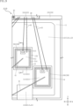
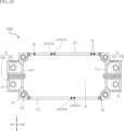
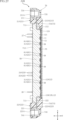
- FIG. 1 is a perspective view of a semiconductor device according to a first embodiment of the present disclosure.
- FIG. 2 is a plan view of the semiconductor device shown in FIG. 1.
- FIG. 3 is a plan view corresponding to FIG. 2, in which the sealing resin is seen through.
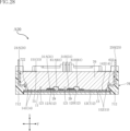
- FIG. 4 is a bottom view of the semiconductor device shown in FIG. 1.
- FIG. 5 is a front view of the semiconductor device shown in FIG. 1.
- FIG. 6 is a right side view of the semiconductor device shown in FIG. 1.
- FIG. 7 is a sectional view taken along line VII-VII in FIG. 3.
- FIG. 8 is a cross-sectional view taken along line VIII-VIII in FIG. 3.
- FIG. 9 is a partially enlarged view of FIG. 3, showing a plurality of first elements and their vicinity.
- FIG. 10 is a cross-sectional view taken along line XX in FIG.
- FIG. 11 is a partially enlarged view of FIG. 10.
- FIG. 12 is a partially enlarged view of FIG. 3, showing a plurality of second elements and their vicinity.
- FIG. 13 is a sectional view taken along line XIII-XIII in FIG. 12.
- FIG. 14 is a partially enlarged plan view of a semiconductor device according to a first modification of the first embodiment of the present disclosure, and corresponds to FIG. 9.
- FIG. 15 is a partially enlarged plan view of a semiconductor device according to a second modification of the first embodiment of the present disclosure, and corresponds to FIG. 9.
- FIG. 9 is a partially enlarged plan view of a semiconductor device according to a second modification of the first embodiment of the present disclosure, and corresponds to FIG. 9.
- FIG. 16 is a partially enlarged plan view of a semiconductor device according to a third modification of the first embodiment of the present disclosure, and corresponds to FIG. 9.
- FIG. 17 is a partially enlarged sectional view of a semiconductor device according to a fourth modification of the first embodiment of the present disclosure, and corresponds to FIG. 11.
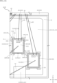
- FIG. 18 is a perspective view of a semiconductor device according to a second embodiment of the present disclosure.
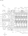
- FIG. 19 is a plan view of the semiconductor device shown in FIG. 18.
- FIG. 20 is a plan view of the semiconductor device shown in FIG. 18, through which the sealing resin is seen.
- FIG. 21 is a front view of the semiconductor device shown in FIG. 18.
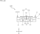
- 22 is a right side view of the semiconductor device shown in FIG. 18.
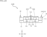
- 23 is a left side view of the semiconductor device shown in FIG. 18.
- FIG. 24 is a bottom view of the semiconductor device shown in FIG. 18.
- FIG. 25 is a partially enlarged view of FIG. 20.
- FIG. 26 is a partially enlarged view of FIG. 20.
- FIG. 27 is a cross-sectional view taken along line XXVII-XXVII in FIG. 20.
- FIG. 28 is a cross-sectional view taken along line XXVIII-XXVIII in FIG. 20.
- FIG. 29 is a cross-sectional view taken along line XXIX-XXIX in FIG. 20.
- FIG. 30 is a sectional view taken along the line XXX-XXX in FIG. 20.
- FIG. 31 is a partially enlarged view of FIG. 25, showing one of the plurality of first elements and its vicinity.
- FIG. 32 is a sectional view taken along line XXXII-XXXII in FIG. 31.
- FIG. 33 is a partially enlarged view of FIG. 25, showing one of the plurality of second elements and its vicinity.
- FIG. 34 is a sectional view taken along line XXXIV-XXXIV in FIG. 33.
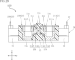
- the semiconductor device A10 includes an insulating layer 11, a plurality of conductive layers 12, a heat dissipation layer 13, a plurality of input terminals 21, a plurality of output terminals 22, a plurality of semiconductor elements 31, a bonding layer 39, a plurality of first wires 41, a plurality of A second wire 42 and a sealing resin 50 are provided.
- the semiconductor device A10 includes a plurality of control terminals 23, a dummy terminal 29, a plurality of ICs 33, a plurality of diodes 34, a plurality of third wires 43, a plurality of fourth wires 44, a plurality of fifth wires 45, and a plurality of sixth wires.
- a wire 46 is provided.
- the sealing resin 50 is shown.
- the transparent sealing resin 50 is shown by an imaginary line (two-dot chain line).
- the VII-VII line and the VIII-VIII line are each shown by a dashed-dotted line.
- first direction z the normal direction of the main surface 121 of the conductive layer 12, which will be described later, will be referred to as a "first direction z.”
- second direction x One direction perpendicular to the first direction z
- third direction y A direction perpendicular to the first direction z and the second direction x is referred to as a "third direction y.”
- the semiconductor device A10 converts DC power input to the plurality of input terminals 21 into AC power using the plurality of semiconductor elements 31.
- the converted AC power is output from the plurality of output terminals 22 as three phases (U phase, V phase, W phase) each having a different phase.
- the semiconductor device A10 is an IPM (Intelligent Power Module).
- the semiconductor device A10 is used, for example, in a power supply circuit for driving a three-phase AC motor.
- the insulating layer 11 supports a plurality of conductive layers 12, as shown in FIGS. 3, 7, and 8.
- the insulating layer 11 is made of ceramics containing aluminum nitride (AlN), for example.
- AlN aluminum nitride
- the insulating layer 11 has a rectangular shape with the second direction x as the long side direction.
- the plurality of conductive layers 12 are bonded to the insulating layer 11, as shown in FIGS. 7 and 8.
- the composition of the plurality of conductive layers 12 includes copper (Cu).
- the plurality of conductive layers 12 are surrounded by the outer edge of the insulating layer 11 when viewed in the first direction z.
- the dimension of each of the plurality of conductive layers 12 in the first direction z is larger than the dimension of the insulating layer 11 in the first direction z.
- each of the plurality of conductive layers 12 has a main surface 121.
- the main surface 121 faces the side opposite to the side facing the insulating layer 11 in the first direction z.
- the plurality of conductive layers 12 include a first conductive layer 12A and a plurality of second conductive layers 12B.
- the plurality of second conductive layers 12B are located on one side of the first conductive layer 12A in the second direction x.
- the heat dissipation layer 13 is located on the opposite side of the plurality of conductive layers 12 with respect to the insulating layer 11.
- the heat dissipation layer 13 is bonded to the insulating layer 11.
- the composition of the heat dissipation layer 13 includes copper.
- the heat dissipation layer 13 is surrounded by the outer edge of the insulating layer 11 when viewed in the first direction z.
- the dimension of the heat dissipation layer 13 in the first direction z is larger than the dimension of the insulating layer 11 in the first direction z.
- the insulating layer 11, the plurality of conductive layers 12, and the heat dissipation layer 13 are obtained from a DBC (Direct Bonded Copper) substrate.
- the plurality of conductive layers 12 and heat dissipation layer 13 are formed by etching a copper foil that forms part of the DBC board.
- Each of the plurality of semiconductor elements 31 is bonded to one of the main surfaces 121 of the plurality of conductive layers 12, as shown in FIGS. 3 and 7.
- the multiple semiconductor elements 31 include multiple first elements 31A and multiple second elements 31B.
- the plurality of first elements 31A are joined to the main surface 121 of the first conductive layer 12A among the plurality of conductive layers 12.
- the plurality of second elements 31B are individually bonded to the main surface 121 of each of the plurality of second conductive layers 12B among the plurality of conductive layers 12.
- the plurality of semiconductor elements 31 are, for example, MOSFETs (Metal-Oxide-Semiconductor Field-Effect Transistors). In addition, the plurality of semiconductor elements 31 may be switching elements such as IGBTs (Insulated Gate Bipolar Transistors), or diodes. In the description of the semiconductor device A10, the plurality of semiconductor elements 31 are n-channel type MOSFETs with a vertical structure.
- the plurality of semiconductor elements 31 include a compound semiconductor substrate.
- the composition of the compound semiconductor substrate includes silicon carbide (SiC). As shown in FIG. 9, the plurality of semiconductor elements 31 have a first electrode 311, a second electrode 312, and a gate electrode 313.
- the first electrode 311 faces one of the main surfaces 121 of the plurality of conductive layers 12. A current corresponding to the power before being converted by the semiconductor element 31 flows through the first electrode 311 . That is, the first electrode 311 corresponds to the drain electrode of the semiconductor element 31.
- the second electrode 312 is located on the opposite side from the first electrode 311 in the first direction z. A current corresponding to the power converted by the semiconductor element 31 flows through the second electrode 312 . That is, the second electrode 312 corresponds to the source electrode of the semiconductor element 31.
- the second electrode 312 includes multiple metal plating layers.
- the second electrode 312 includes a nickel (Ni) plating layer and a gold (Au) plating layer stacked on the nickel plating layer.
- the second electrode 312 may include a nickel plating layer, a palladium (Pd) plating layer laminated on the nickel plating layer, and a gold plating layer laminated on the palladium plating layer. good.
- the gate electrode 313 is provided on the same side as the second electrode 312 in the first direction z, and is located away from the second electrode 312. A gate voltage for driving the semiconductor element 31 is applied to the gate electrode 313 . As shown in FIG. 10, the area of the gate electrode 313 is smaller than the area of the second electrode 312 when viewed in the first direction z.
- the bonding layer 39 bonds one of the main surfaces 121 of the plurality of conductive layers 12 to one of the plurality of semiconductor elements 31.
- the first electrode 311 of each of the plurality of first elements 31A is conductively bonded to the main surface 121 of the first conductive layer 12A via the bonding layer 39.
- the first electrode 311 of each of the plurality of second elements 31B is individually conductively bonded to the main surface 121 of each of the plurality of second conductive layers 12B via the bonding layer 39.
- Bonding layer 39 is solder.
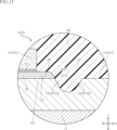
- each of the plurality of conductive layers 12 is provided with at least one recess 19.
- the recessed portion 19 is recessed from one of the main surfaces 121 of the plurality of conductive layers 12 .
- a plurality of recesses 19 are provided in the first conductive layer 12A. When viewed in the first direction z, the plurality of recesses 19 provided in the first conductive layer 12A individually surround the plurality of first elements 31A.
- Each of the plurality of second conductive layers 12B is provided with a recessed portion 19 located around any one of the plurality of second elements 31B.
- the bonding layer 39 has a first portion 391 located between any one of the plurality of semiconductor elements 31 and the recess 19 when viewed in the first direction z. As shown in FIGS. 10 and 13, the first portion 391 covers any main surface 121 of the plurality of conductive layers 12. As shown in FIGS. 9 and 12, the bonding layer 39 has a first portion 391 located between any one of the plurality of semiconductor elements 31 and the recess 19 when viewed in the first direction z. As shown in FIGS. 10 and 13, the first portion 391 covers any main surface 121 of the plurality of conductive layers 12. As shown in FIGS.
- each of the plurality of conductive layers 12 has an inner peripheral surface 122.
- the inner circumferential surface 122 is connected to one of the main surfaces 121 of the plurality of conductive layers 12 and defines the recess 19 .
- the first portion 391 of the bonding layer 39 is in contact with the boundary 121A between the inner peripheral surface 122 and the main surface 121.
- An end surface 391A of the first portion 391 is inclined with respect to the main surface 121.
- the reason why the end surface 391A is inclined with respect to the main surface 121 is that when bonding each of the plurality of semiconductor elements 31 to one of the plurality of conductive layers 12, surface tension acts on the melted bonding layer 39 at the boundary 121A. This is to do so.
- the inner circumferential surface 122 has a first circumferential surface 122A, a second circumferential surface 122B, and a third circumferential surface 122C.
- the first circumferential surface 122A and the second circumferential surface 122B face each other in a direction perpendicular to the first direction z.
- the first circumferential surface 122A is located closest to any one of the plurality of semiconductor elements 31.
- the first circumferential surface 122A and the second circumferential surface 122B become closer to each other in the first direction z from one of the main surfaces 121 of the plurality of conductive layers 12 toward the insulating layer 11.
- Each of the first circumferential surface 122A and the second circumferential surface 122B is curved inward of any one of the plurality of conductive layers 12.
- the third circumferential surface 122C is connected to the first circumferential surface 122A and the second circumferential surface 122B.
- the third peripheral surface 122C faces the same side as the main surface 121 in the first direction z.
- the first conductive layer 12A has a plurality of pedestals 123.
- the plurality of pedestals 123 are individually surrounded by the plurality of recesses 19 provided in the first conductive layer 12A.
- Each of the plurality of pedestals 123 includes the main surface 121 of the first conductive layer 12A.
- the first electrode 311 of each of the plurality of first elements 31A is individually conductively bonded to the main surface 121 of each of the plurality of pedestals 123 via the bonding layer 39.
- the cross-sectional area of each of the plurality of pedestals 123 in the first direction z increases from the main surface 121 of the first conductive layer 12A toward the insulating layer 11.
- the recess 19 provided in each of the plurality of second conductive layers 12B is located at the peripheral edge 314 of any one of the plurality of second elements 31B when viewed in the first direction z. extending in the intersecting direction.
- the recess 19 includes a first recess 19A, a second recess 19B, a third recess 19C, and a fourth recess 19D.
- the first recess 19A, the second recess 19B, the third recess 19C, and the fourth recess 19D are separated from each other.
- the first recess 19A and the second recess 19B are located on opposite sides of the second element 31B in the second direction x.
- the third recess 19C and the fourth recess 19D are located on opposite sides of the second element 31B in the third direction y.
- Each of the first recess 19A, the second recess 19B, the third recess 19C, and the fourth recess 19D includes two separate parts.
- the plurality of input terminals 21, together with the plurality of output terminals 22, the plurality of control terminals 23, and the dummy terminals 29, are composed of the same lead frame.
- the lead frame is made of a material containing copper (Cu) or a copper alloy. Therefore, the compositions of the plurality of input terminals 21, the plurality of output terminals 22, the plurality of control terminals 23, and the dummy terminal 29 include copper.
- the plurality of input terminals 21 include a first input terminal 21A and a plurality of second input terminals 21B.
- the plurality of second input terminals 21B are located on the opposite side of the first input terminal 21A with respect to the plurality of output terminals 22.
- Each of the plurality of input terminals 21 has an external connection section 211 and an internal connection section 212.
- the external connection portion 211 is exposed to the outside from the sealing resin 50.
- the internal connection part 212 is connected to the external connection part 211 and is covered with the sealing resin 50.
- the internal connection portion 212 of the first input terminal 21A is conductively bonded to the main surface 121 of the first conductive layer 12A via the bonding layer 39.
- the first input terminal 21A corresponds to a P terminal (positive electrode) into which DC power to be converted is input.
- the plurality of second input terminals 21B are separated from the insulating layer 11.
- the plurality of second input terminals 21B are supported by the sealing resin 50.
- the plurality of second input terminals 21B are separated from the plurality of conductive layers 12 when viewed in the first direction z.
- the plurality of second input terminals 21B correspond to an N terminal (negative electrode) into which DC power to be converted is input.
- the plurality of output terminals 22 are located between the first input terminal 21A and the plurality of second input terminals 21B in the second direction x.
- the plurality of output terminals 22 include a first output terminal 22A, a second output terminal 22B, and a third output terminal 22C.
- Each of the output terminals 22 has an external connection part 221 and an internal connection part 222.
- the external connection portion 221 is exposed to the outside from the sealing resin 50.
- the internal connection part 222 is connected to the external connection part 221 and is covered with the sealing resin 50.
- each of the plurality of output terminals 22 are individually conductively bonded to the main surface 121 of each of the plurality of second conductive layers 12B via the bonding layer 39.
- Three-phase AC power converted by the plurality of semiconductor elements 31 is output from the plurality of output terminals 22 .
- the plurality of first wires 41 are individually conductively joined to the second electrode 312 of each of the plurality of first elements 31A and the internal connection part 222 of each of the plurality of output terminals 22. There is. Thereby, the second electrodes 312 of each of the plurality of first elements 31A are individually electrically connected to the plurality of second conductive layers 12B. Furthermore, the first electrode 311 of each of the plurality of second elements 31B is electrically connected to the second electrode 312 of any one of the plurality of first elements 31A.
- the composition of the plurality of first wires 41 includes aluminum (Al). In addition, the composition of the plurality of first wires 41 may include copper.
- the plurality of second wires 42 are individually conductively bonded to the second electrodes 312 of the plurality of second elements 31B and the plurality of second input terminals 21B. Thereby, the second electrode 312 of each of the plurality of second elements 31B is individually electrically connected to the plurality of second input terminals 21B.
- the composition of the plurality of second wires 42 includes aluminum. In addition, the composition of the plurality of second wires 42 may include copper.
- a plurality of upper arm circuits are configured by the first conductive layer 12A, the plurality of first elements 31A, and the plurality of first wires 41.
- a plurality of lower arm circuits are configured by the plurality of second conductive layers 12B, the plurality of second elements 31B, the plurality of second wires 42, and the plurality of second input terminals 21B. Therefore, the voltage applied to the gate electrode 313 of each of the plurality of first elements 31A is different from the voltage applied to the gate electrode 313 of each of the plurality of second elements 31B. Further, since the semiconductor device A10 includes the plurality of second input terminals 21B, the grounds of the plurality of lower arm circuits are individually set in the semiconductor device A10.
- the plurality of control terminals 23 are located on the opposite side of the plurality of input terminals 21 and the plurality of output terminals 22 with respect to the plurality of conductive layers 12 in the third direction y.
- the plurality of control terminals 23 are located apart from the insulating layer 11 and supported by the sealing resin 50, similarly to the plurality of second input terminals 21B. As shown in FIGS. 2 and 4, a portion of each of the plurality of control terminals 23 is exposed to the outside from the sealing resin 50.
- the plurality of control terminals 23 include a pad section 231, a plurality of power supply sections 232, a plurality of first control sections 233, a plurality of second control sections 234, and a dummy section 235.
- the pad section 231 has a plurality of ICs 33 mounted thereon. Further, the pad portion 231 serves as a ground for the plurality of ICs 33.
- the plurality of ICs 33 are located on the opposite side of the plurality of input terminals 21 and the plurality of output terminals 22 with respect to the plurality of conductive layers 12 in the third direction y.
- the plurality of ICs 33 include a first IC 33A and a second IC 33B that are separated from each other in the second direction x.
- the plurality of power supply units 232 are inputted with a power source that is the basis of the gate voltage for driving the plurality of first elements 31A.
- Electric signals related to control of the first IC 33A are input and output to the plurality of first control units 233.
- Electric signals related to control of the second IC 33B are input and output to the plurality of second control units 234.
- the dummy portion 235 is not electrically connected to the plurality of ICs 33.
- the first IC 33A is bonded to the pad portion 231 via the bonding layer 39. As shown in FIG. 3, the first IC 33A is located closer to the first conductive layer 12A than the second IC 33B. The first IC 33A applies a gate voltage to the gate electrodes 313 of the plurality of first elements 31A.
- the second IC 33B is bonded to the pad portion 231 via the bonding layer 39, similarly to the first IC 33A. As shown in FIG. 3, the second IC 33B is located closer to the plurality of second conductive layers 12B than the first IC 33A. The second IC 33B applies a gate voltage to the gate electrodes 313 of the plurality of second elements 31B.
- the plurality of diodes 34 are individually conductively bonded to the plurality of power supply sections 232 via the bonding layer 39.
- the plurality of diodes 34 prevent reverse bias from being applied to the plurality of power supply sections 232 as the plurality of first elements 31A are driven.
- the plurality of third wires 43 are conductively bonded to the first IC 33A and the second electrode 312 and gate electrode 313 of each of the plurality of first elements 31A.
- a gate voltage is applied from the first IC 33A to the gate electrodes 313 of the plurality of first elements 31A.
- the ground of the gate voltage is set in the first IC 33A.
- the composition of the plurality of third wires 43 includes, for example, gold.
- the plurality of fourth wires 44 are electrically connected to the second IC 33B and the gate electrode 313 of each of the plurality of second elements 31B. Thereby, a gate voltage is applied from the second IC 33B to the gate electrodes 313 of the plurality of second elements 31B.
- the composition of the plurality of fourth wires 44 includes, for example, gold.
- the plurality of fifth wires 45 are electrically connected to the first IC 33A, the pad section 231, the plurality of power supply sections 232, the plurality of diodes 34, and the plurality of first control sections 233.
- the pad section 231, the plurality of power supply sections 232, the plurality of diodes 34, and the plurality of first control sections 233 are electrically connected to the first IC 33A.
- the composition of the plurality of fifth wires 45 includes, for example, gold.
- the plurality of sixth wires 46 are connected to the second IC 33B, the pad section 231, and the plurality of second control sections 234. Thereby, the pad section 231 and the plurality of second control sections 234 are electrically connected to the second IC 33B.
- the composition of the plurality of sixth wires 46 includes, for example, gold.
- the dummy terminal 29 is separated from the insulating layer 11 when viewed in the first direction z.
- the dummy terminal 29 is located on the opposite side of the plurality of output terminals 22 with respect to the first input terminal 21A in the second direction x.
- a portion of the dummy terminal 29 is exposed to the outside through the sealing resin 50.
- the sealing resin 50 connects the plurality of conductive layers 12, the plurality of semiconductor elements 31, the plurality of ICs 33, the internal connection portions 212 of each of the plurality of input terminals 21, and the plurality of output terminals. 22. Furthermore, the sealing resin 50 covers a portion of each of the plurality of control terminals 23 and a portion of the dummy terminal 29.
- the sealing resin 50 has electrical insulation properties.
- the sealing resin 50 is made of a material containing, for example, a black epoxy resin. As shown in FIGS. 10 and 13, a portion of the sealing resin 50 has entered the recess 19 provided in each of the plurality of conductive layers 12.
- the sealing resin 50 has a top surface 51 , a bottom surface 52 , a pair of first side surfaces 53 , a pair of second side surfaces 54 , and a pair of recessed portions 55 .
- the top surface 51 faces the same side as the main surfaces 121 of the plurality of conductive layers 12 in the first direction z.
- the bottom surface 52 faces opposite to the main surface 121 in the first direction z. Therefore, the top surface 51 and the bottom surface 52 face oppositely to each other in the first direction z.
- the heat dissipation layer 13 is exposed to the outside from the bottom surface 52.
- the pair of first side surfaces 53 are located apart from each other in the second direction x.
- a pair of first side surfaces 53 are connected to the top surface 51 and the bottom surface 52.
- the pair of second side surfaces 54 are located apart from each other in the third direction y.
- a pair of second side surfaces 54 are connected to the top surface 51 and the bottom surface 52. From one second side surface 54 of the pair of second side surfaces 54, the external connection portions 211 of each of the plurality of input terminals 21, the external connection portions 221 of each of the plurality of output terminals 22, and a part of the dummy terminal 29 are connected. is exposed to the outside. A portion of each of the plurality of control terminals 23 is exposed to the outside from the other second side surface 54 of the pair of second side surfaces 54 .
- the pair of recessed portions 55 are recessed from the pair of first side surfaces 53 in the second direction x. In the first direction z, the pair of invaginations 55 extend from the top surface 51 to the bottom surface 52.
- the pair of recessed portions 55 ensure a longer creepage distance of the sealing resin 50 from the external connection portion 211 of any one of the plurality of input terminals 21 to any one of the plurality of control terminals 23. In addition, a longer creepage distance of the sealing resin 50 from any one of the plurality of second input terminals 21B to any one of the plurality of control terminals 23 is ensured. This is suitable for improving the dielectric strength of the semiconductor device A10.
- each of the plurality of recesses 19 provided in the first conductive layer 12A is located on the peripheral edge 314 of any one of the plurality of first elements 31A when viewed in the first direction z. It extends along.
- Each of the plurality of recesses 19 includes a first recess 19A, a second recess 19B, a third recess 19C, and a fourth recess 19D.
- the first recess 19A and the second recess 19B are located on opposite sides of the first element 31A in the second direction x.
- the third recess 19C and the fourth recess 19D are located on opposite sides of the first element 31A in the third direction y.
- each of the first recess 19A, the second recess 19B, the third recess 19C, and the fourth recess 19D is single.
- each of the first recess 19A, the second recess 19B, the third recess 19C, and the fourth recess 19D may include two separate parts as shown in FIG. 12.
- each of the plurality of recesses 19 provided in the first conductive layer 12A is located on the peripheral edge 314 of any one of the plurality of first elements 31A when viewed in the first direction z. It extends along.
- Each of the plurality of recesses 19 includes a first recess 19A, a second recess 19B, a third recess 19C, and a fourth recess 19D.
- Each of the first recess 19A, the second recess 19B, the third recess 19C, and the fourth recess 19D is located closest to one of the four corners of the first element 31A.
- the peripheral edge 314 of the first element 31A has a first peripheral edge 314A and a second peripheral edge 314B.
- the second peripheral edge 314B extends in a different direction from the first peripheral edge 314A and is connected to the first peripheral edge 314A.
- Each of the first recess 19A, the second recess 19B, the third recess 19C, and the fourth recess 19D has a first groove 191 and a second groove 192.
- the first groove 191 extends along the first peripheral edge 314A.
- the second groove 192 extends along the second peripheral edge 314B and is connected to the first groove 191.
- the first groove 191 and the extension line EL2 of the second peripheral edge 314B intersect.
- the second groove 192 and the extension line EL1 of the first peripheral edge 314A intersect.
- each of the plurality of recesses 19 provided in the first conductive layer 12A is located on the peripheral edge 314 of any one of the plurality of first elements 31A when viewed in the first direction z. extending in the intersecting direction.
- Each of the plurality of recesses 19 includes a first recess 19A, a second recess 19B, a third recess 19C, and a fourth recess 19D.
- the first recess 19A and the second recess 19B are located on opposite sides of the first element 31A.
- the third recess 19C and the fourth recess 19D are located on opposite sides of the first element 31A.
- Each of the first recess 19A, the second recess 19B, the third recess 19C, and the fourth recess 19D is located closest to one of the four corners of the first element 31A.
- FIG. 17 a semiconductor device A14, which is a fourth modification example of the semiconductor device A10, will be described.
- the position in FIG. 17 corresponds to the position in FIG.
- the inner peripheral surface 122 does not include the third peripheral surface 122C.
- the semiconductor device A10 includes a conductive layer 12 bonded to an insulating layer 11, a semiconductor element 31 bonded to a main surface 121 of the conductive layer 12, and a bonding layer 39 bonding the main surface 121 and the semiconductor element 31. .
- the conductive layer 12 is provided with a recess 19 recessed from the main surface 121 .
- the bonding layer 39 has a first portion 391 located between the semiconductor element 31 and the recess 19 when viewed in the first direction z. The first portion 391 covers the main surface 121.
- the wetting and spreading of the bonding layer 39 is suppressed, and therefore the movement of the semiconductor element 31 due to the wetting and spreading of the bonding layer 39 is also suppressed. Therefore, according to this configuration, in the semiconductor device A10, it is possible to further improve the accuracy of the bonding position of the semiconductor element 31 to the conductive layer 12.
- the above effects can also be obtained by providing the conductive layer 12 with a slit that penetrates the conductive layer 12 in the first direction z near the bonding position of the semiconductor element 31.
- the recess 19 is used instead of the slit.
- the volume reduction of the conductive layer 12 is further reduced, so that it is possible to suppress a decrease in thermal conductivity of the conductive layer 12 in the direction perpendicular to the first direction z.
- the conductive layer 12 has an inner circumferential surface 122 that is connected to the main surface 121 and defines the recess 19 .
- the inner circumferential surface 122 has a first circumferential surface 122A and a second circumferential surface 122B that face each other in a direction orthogonal to the first direction z.
- the first circumferential surface 122A and the second circumferential surface 122B approach each other as they go from the main surface 121 toward the insulating layer 11.
- the size of the recess 19 can be set as small as possible. Thereby, the volume reduction of the conductive layer 12 can be further reduced.
- the recess 19 surrounds the semiconductor element 31 when viewed in the first direction z.
- the conductive layer 12 has a pedestal portion 123 surrounded by the recess 19.
- the cross-sectional area of the pedestal portion 123 in the first direction z increases from the main surface 121 of the conductive layer 12 toward the insulating layer 11.
- the peripheral edge 314 of the semiconductor element 31 When viewed in the first direction z, the peripheral edge 314 of the semiconductor element 31 has a first peripheral edge 314A and a second peripheral edge 314B that extends in a direction different from the first peripheral edge 314A and is connected to the first peripheral edge 314A.
- the recess 19 has a first groove 191 extending along the first peripheral edge 314A and a second groove 192 extending along the second peripheral edge 314B and connected to the first groove 191.
- the first groove 191 intersects with the extension line EL2 of the second peripheral edge 314B
- the second groove 192 intersects with the extension line EL1 of the first peripheral edge 314A (see FIG. 15).
- the recess 19 includes a first recess 19A and a second recess 19B separated from the first recess 19A.
- the first recess 19A and the second recess 19B are located on opposite sides with respect to the semiconductor element 31. Even with this configuration, when bonding the semiconductor element 31 to the main surface 121 of the conductive layer 12 via the bonding layer 39, wetting and spreading of the bonding layer 39 can be suppressed.
- the semiconductor device A10 further includes a sealing resin 50 that covers the semiconductor element 31.
- a portion of the sealing resin 50 has entered the recess 19.
- the sealing resin 50 has a bottom surface 52 facing opposite to the main surface 121 of the conductive layer 12 in the first direction z.
- the heat dissipation layer 13 is exposed from the bottom surface 52.
- FIGS. 18 to 34 A semiconductor device A20 according to a second embodiment of the present disclosure will be described based on FIGS. 18 to 34.
- elements that are the same as or similar to those of the semiconductor device A10 described above are denoted by the same reference numerals, and redundant explanation will be omitted.
- FIG. 20 FIG. 25, and FIG. 26, illustration of the sealing resin 50 is omitted for convenience of understanding.
- FIG. 20 the XXVII-XXVII line and the XXVIII-XXVIII line are each shown by a dashed-dotted line.
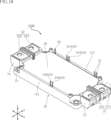
- the semiconductor device A20 includes an insulating layer 11, a plurality of conductive layers 12, a heat dissipation layer 13, a plurality of input terminals 21, an output terminal 22, a plurality of semiconductor elements 31, and a sealing resin 50. Further, the semiconductor device A20 includes a plurality of gate wirings 14, a plurality of detection wirings 15, a plurality of gate terminals 24, a plurality of detection terminals 25, and a case 70.
- the semiconductor device A20 is a power module.
- the semiconductor device A20 is used in inverters for electrical products, hybrid vehicles, and the like. As shown in FIGS. 18 and 19, the semiconductor device A20 has a rectangular shape (or a substantially rectangular shape) when viewed in the first direction z.
- the second direction x corresponds to the longitudinal direction of the semiconductor device A20.
- the insulating layer 11 is bonded to the heat radiating member 75 via the heat radiating layer 13, as shown in FIGS. 27 and 28. As shown in FIG. 24, a portion of the heat dissipation member 75 is exposed to the outside of the semiconductor device A20.
- the heat radiation member 75 is, for example, a flat metal plate.
- the composition of the metal plate includes copper.
- the surface of the heat dissipating member 75 may be plated with nickel.
- the dimension of the heat dissipation member 75 in the first direction z is larger than the dimension of the heat dissipation layer 13 in the first direction z.
- the plurality of conductive layers 12 include a first conductive layer 12A, a second conductive layer 12B, and a third conductive layer 12C.
- Each of the first conductive layer 12A, the second conductive layer 12B, and the third conductive layer 12C extends in the second direction x.
- the second conductive layer 12B is located on one side of the first conductive layer 12A in the third direction y.
- the third conductive layer 12C is located on the opposite side of the first conductive layer 12A with respect to the second conductive layer 12B in the third direction y.
- a plurality of recesses 19 are provided in each of the first conductive layer 12A and the second conductive layer 12B.
- each of the plurality of recesses 19 provided in the first conductive layer 12A individually surrounds the plurality of first elements 31A.
- each of the plurality of recesses 19 provided in the second conductive layer 12B individually surrounds the plurality of second elements 31B.
- the plurality of gate wirings 14 are joined to the insulating layer 11 so as to be on the same side as the plurality of conductive layers 12 in the first direction z.
- the plurality of gate wirings 14 include a first gate wiring 141 and a second gate wiring 142.
- the first gate wiring 141 is located on the opposite side of the second conductive layer 12B with the first conductive layer 12A interposed therebetween in the third direction y.
- the first gate wiring 141 extends in the second direction x.
- the first gate wiring 141 includes two portions separated from each other in the third direction y. One ends of the two portions of the first gate wiring 141 located closest to the plurality of input terminals 21 are connected to each other.
- the second gate wiring 142 is located on the opposite side of the second conductive layer 12B with the third conductive layer 12C interposed therebetween in the third direction y.
- the second gate wiring 142 extends in the second direction x.
- the second gate wiring 142 includes two parts separated from each other in the third direction y. One ends of the two portions of the second gate wiring 142 located closest to the output terminal 22 are connected to each other.
- the plurality of detection wirings 15 are joined to the insulating layer 11 so as to be on the same side as the plurality of conductive layers 12 in the first direction z.
- the plurality of detection wirings 15 include a first detection wiring 161 and a second detection wiring 162.
- the first detection wiring 161 is located next to the first gate wiring 141 in the third direction y.
- the first detection wiring 161 extends in the second direction x.
- the first detection wiring 161 includes two parts separated from each other in the third direction y. One ends of the two portions of the first detection wiring 161 located closest to the output terminal 22 are connected to each other.
- the second detection wiring 162 is located next to the second gate wiring 142 in the third direction y.
- the second detection wiring 162 extends in the second direction x.
- the second detection wiring 162 includes two parts separated from each other in the third direction y. One ends of the two portions of the second detection wiring 162 located closest to the plurality of input terminals 21 are connected to each other.
- the semiconductor device A20 further includes a pair of pads 16.
- the pair of pads 16 are bonded to the insulating layer 11 on the same side as the plurality of conductive layers 12 in the first direction z.
- the pair of pads 16 are adjacent to each other in the second direction x.
- the pair of pads 16 are located at the corners of the insulating layer 11.
- the pair of pads 16 are close to the first conductive layer 12A.
- the plurality of input terminals 21 are part of external connection terminals provided in the semiconductor device A20, as shown in FIGS. 19 and 20.
- the plurality of input terminals 21 are connected to a DC power supply placed outside the semiconductor device A20.
- the plurality of input terminals 21 are supported by the case 70.
- the plurality of input terminals 21 are composed of metal plates.
- the metal plate contains copper, for example.
- the plurality of input terminals 21 include a first input terminal 21A and a second input terminal 21B.
- the first input terminal 21A is a positive electrode (P terminal).
- the first input terminal 21A is bonded to the bonding portion 124 of the first conductive layer 12A. Thereby, the first input terminal 21A is electrically connected to the first conductive layer 12A.
- the second input terminal 21B is a negative electrode (N terminal).
- the second input terminal 21B is joined to the joint portion 124 of the third conductive layer 12C. Thereby, the second input terminal 21B is electrically connected to the third conductive layer 12C.
- the first input terminal 21A and the second input terminal 21B are adjacent to each other in the third direction y.
- each of the first input terminal 21A and the second input terminal 21B has an external connection portion 211, an internal connection portion 212, and an intermediate portion 213.
- the external connection portion 211 is exposed from the semiconductor device A20 and has a flat plate shape orthogonal to the first direction z.
- a DC power cable or the like is connected to the external connection portion 211 .
- External connection section 211 is supported by case 70.
- the external connection portion 211 is provided with a connection hole 211A penetrating in the first direction z.
- a fastening member such as a bolt is inserted into the connection hole 211A.
- the surface of the external connection portion 211 may be plated with nickel (Ni).
- the internal connection portion 212 of the first input terminal 21A is conductively bonded to the bonding portion 124 of the first conductive layer 12A.
- the internal connection portion 212 of the second input terminal 21B is conductively bonded to the bonding portion 124 of the third conductive layer 12C.
- the internal connection part 212 has a plurality of teeth arranged along the third direction y. The plurality of teeth are bent in the first direction z. Therefore, the plurality of teeth have a hook shape when viewed in the third direction y.
- the plurality of teeth are conductively bonded to the bonding portion 124 of either the first conductive layer 12A or the third conductive layer 12C by ultrasonic vibration.
- the intermediate portion 213 interconnects the external connection portion 211 and the internal connection portion 212.
- the intermediate portion 213 has an L-shaped cross section in the second direction x.
- the intermediate portion 213 has a base portion 213A and an upright portion 213B.
- the base 213A extends along the second direction x and the third direction y.
- One end of the base 213A in the second direction x is connected to the internal connection part 212.
- the standing portion 213B stands up in the first direction z from the base portion 213A.
- One end of the upright portion 213B in the first direction z is connected to the external connection portion 211.
- the output terminal 22 is a part of the external connection terminal provided in the semiconductor device A20, as shown in FIGS. 19 and 20.
- the output terminal 22 is connected to a power supply target (such as a motor) placed outside the semiconductor device A20.
- the output terminal 22 is supported by the case 70 and is located on the opposite side of the insulating layer 11 from the plurality of input terminals 21 in the second direction x.
- the output terminal 22 is made of a metal plate.
- the metal plate contains copper, for example.
- the output terminal 22 is separated into two, a first output terminal 22A and a second output terminal 22B.
- the output terminal 22 may be a single member in which the first output terminal 22A and the second output terminal 22B are integrated.
- the first output terminal 22A and the second output terminal 22B are electrically conductively bonded to the bonding portion 124 of the second conductive layer 12B. Thereby, the output terminal 22 is electrically connected to the second conductive layer 12B.
- the first output terminal 22A and the second output terminal 22B are adjacent to each other in the third direction y.
- each of the first output terminal 22A and the second output terminal 22B has an external connection portion 221, an internal connection portion 222, and an intermediate portion 223.
- the external connection portion 221 is exposed from the semiconductor device A20 and has a flat plate shape orthogonal to the first direction z. A cable or the like that is electrically connected to the object to be supplied with power is connected to the external connection portion 221 . External connection section 221 is supported by case 70.
- the external connection portion 221 is provided with a connection hole 221A that penetrates in the first direction z. A fastening member such as a bolt is inserted into the connection hole 221A. Note that the surface of the external connection portion 211 may be plated with nickel.
- the internal connection portion 222 is conductively bonded to the bonding portion 124 of the second conductive layer 12B.
- the internal connection part 222 has a plurality of teeth arranged along the third direction y.
- the plurality of teeth are bent in the first direction z. Therefore, the plurality of teeth have a hook shape when viewed in the third direction y.
- the plurality of teeth are electrically conductively bonded to the bonding portion 124 of the second conductive layer 12B by ultrasonic vibration.
- the intermediate portion 223 interconnects the external connection portion 221 and the internal connection portion 222.
- the intermediate portion 223 has an L-shaped cross section in the second direction x.
- the intermediate portion 223 has a base portion 223A and an upright portion 223B.
- the base 223A extends along the second direction x and the third direction y.
- One end of the base portion 223A in the second direction x is connected to the internal connection portion 222.
- the standing portion 223B stands up in the first direction z from the base portion 223A.
- One end of the standing portion 223B in the first direction z is connected to the external connection portion 221.
- the semiconductor device A20 converts DC power input to the plurality of input terminals 21 into AC power using the plurality of semiconductor elements 31.
- the converted AC power is output from the output terminal 22.
- the AC power is supplied to a power supply target such as a motor.
- the plurality of gate terminals 24 are part of external connection terminals provided in the semiconductor device A20, as shown in FIGS. 19 to 21.
- the plurality of gate terminals 24 are electrically connected to the plurality of gate wirings 14.
- the plurality of gate terminals 24 are connected to a drive circuit (gate driver, etc.) of the semiconductor device A20 arranged outside.
- the plurality of gate terminals 24 are supported by the case 70.
- the plurality of gate terminals 24 are composed of metal rods.
- the metal rod contains copper, for example.
- the surfaces of the plurality of gate terminals 24 may be plated with tin (Sn), or may be plated with nickel or tin.
- the plurality of gate terminals 24 have an L-shaped cross section in the second direction x. A portion of each of the plurality of gate terminals 24 protrudes from the case 70 toward the side toward which the main surfaces 121 of the plurality of conductive layers 12 face in the first direction z.
- the plurality of gate terminals 24 include a first gate terminal 24A and a second gate terminal 24B. As shown in FIG. 26, the first gate terminal 24A is close to the first gate wiring 141 in the third direction y. As shown in FIG. 25, the second gate terminal 24B is located on the opposite side of the first gate terminal 24A with respect to the insulating layer 11 in the third direction y. The second gate terminal 24B is close to the second gate wiring 142.
- the plurality of detection terminals 25 are part of the external connection terminals provided in the semiconductor device A20, as shown in FIGS. 19 to 21.
- the plurality of detection terminals 25 are electrically connected to the plurality of detection wirings 15.
- the plurality of detection terminals 25 are connected to a control circuit of an externally arranged semiconductor device A20.
- the plurality of detection terminals 25 are supported by the case 70.
- the plurality of detection terminals 25 are composed of metal rods.
- the metal rod contains copper, for example.
- the surfaces of the plurality of detection terminals 25 may be plated with tin, or may be plated with nickel and tin.
- the plurality of detection terminals 25 have an L-shaped cross section in the second direction x. A portion of each of the plurality of detection terminals 25 protrudes from the case 70 toward the side toward which the main surfaces 121 of the plurality of conductive layers 12 face in the first direction z.
- the plurality of detection terminals 25 include a first detection terminal 25A and a second detection terminal 25B.
- the first detection terminal 25A is located next to the first gate terminal 24A in the second direction x, as shown in FIG.
- the second detection terminal 25B is located next to the second gate terminal 24B in the second direction x.
- the semiconductor device A20 further includes an input current detection terminal 26.
- the input current detection terminal 26 is a part of external connection terminals provided in the semiconductor device A20.
- the input current detection terminal 26 is connected to a control circuit of the semiconductor device A20 placed outside.
- Input current detection terminal 26 is supported by case 70 .
- the input current detection terminal 26 is composed of a metal rod.
- the metal rod contains copper, for example.
- the surface of the input current detection terminal 26 may be plated with tin, or may be plated with nickel and tin.
- the shape of the input current detection terminal 26 is the same as that of the plurality of gate terminals 24 shown in FIG. Like the plurality of gate terminals 24 shown in FIG.
- a part of the input current detection terminal 26 protrudes from the case 70 toward the side toward which the main surfaces 121 of the plurality of conductive layers 12 face in the first direction z.
- the position of the input current detection terminal 26 is the same as the position of the first gate terminal 24A.
- the input current detection terminal 26 is located away from the first gate terminal 24A toward the side where the output terminal 22 is located in the second direction x.
- the semiconductor device A20 further includes an input current detection wire 64.
- the input current detection wire 64 is conductively bonded to the input current detection terminal 26 and the first conductive layer 12A. Thereby, the input current detection terminal 26 is electrically connected to the first conductive layer 12A.
- Input current detection wire 64 is, for example, aluminum.
- the semiconductor device A20 further includes a pair of thermistor terminals 27.
- the pair of thermistor terminals 27 are part of external connection terminals provided in the semiconductor device A20.
- the pair of thermistor terminals 27 are connected to a control circuit of the semiconductor device A20 arranged outside.
- the pair of thermistor terminals 27 are supported by the case 70.
- the pair of thermistor terminals 27 are composed of metal rods.
- the metal rod contains copper, for example.
- the surfaces of the pair of thermistor terminals 27 may be plated with tin, or may be plated with nickel and tin.
- the shape of the pair of thermistor terminals 27 is the same as that of the plurality of gate terminals 24 shown in FIG.
- a portion of the pair of thermistor terminals 27 protrudes from the case 70 toward the side facing the main surfaces 121 of the plurality of conductive layers 12 in the first direction z.
- the position of the pair of thermistor terminals 27 is the same as the position of the first gate terminal 24A.
- the pair of thermistor terminals 27 are separated from the first gate terminal 24A toward the side where the plurality of input terminals 21 are located in the second direction x.
- the pair of thermistor terminals 27 are adjacent to each other in the second direction x.
- the semiconductor device A20 further includes a pair of thermistor wires 65.
- the pair of thermistor wires 65 are individually conductively bonded to the pair of thermistor terminals 27 and the pair of pads 16. Thereby, the pair of input current detection terminals 26 are electrically connected to the pair of pads 16.
- the pair of thermistor wires 65 are made of aluminum, for example.
- the semiconductor device A20 further includes a thermistor 35.
- the thermistor 35 is conductively bonded to the pair of pads 16.
- the thermistor 35 is an NTC (Negative Temperature Coefficient) thermistor.
- the NTC thermistor has a characteristic that its resistance gradually decreases as the temperature rises.
- the thermistor 35 is used as a temperature detection sensor of the semiconductor device A20.
- the thermistor 35 is electrically connected to a pair of thermistor terminals 27 via a pair of pads 16 and a pair of thermistor wires 65.
- the semiconductor device A20 further includes a plurality of conductive members 61, a plurality of first gate wires 621, and a plurality of first detection wires 631, as shown in FIGS. 25 and 26. These are individually conductively bonded to the plurality of semiconductor elements 31.
- the plurality of conductive members 61 are metal clips.
- the composition of the plurality of conductive members 61 includes copper.
- each of the plurality of conductive members 61 may be composed of a plurality of wires.
- the plurality of first gate wires 621 and the plurality of first detection wires 631 are made of aluminum, for example.
- the plurality of conductive members 61 have a first joint 611 and a second joint 612.
- the first bonding portion 611 is conductively bonded to the second electrode 312 of one of the plurality of semiconductor elements 31 via the bonding layer 39 .
- Bonding layer 39 is, for example, solder.
- the second bonding portion 612 is conductively bonded to either the second conductive layer 12B or the third conductive layer 12C among the plurality of conductive layers 12 via the bonding layer 39.
- the plurality of conductive members 61 include a plurality of first conductive members 61A and a plurality of second conductive members 61B.
- the plurality of first conductive members 61A are individually conductively bonded to the second electrodes 312 of the plurality of first elements 31A and the second conductive layer 12B.
- the second electrodes 312 of the plurality of first elements 31A are electrically connected to the second conductive layer 12B. Therefore, the second electrodes 312 of the plurality of first elements 31A are electrically connected to the output terminal 22.
- FIG. 31 the plurality of first conductive members 61A are individually conductively bonded to the second electrodes 312 of the plurality of first elements 31A and the second conductive layer 12B.
- the plurality of second conductive members 61B are individually conductively bonded to the second electrodes 312 of the plurality of second elements 31B and the third conductive layer 12C.
- the second electrodes 312 of the plurality of semiconductor elements 31 are electrically connected to the third conductive layer 12C. Therefore, the second electrodes 312 of the plurality of second elements 31B are electrically connected to the second input terminal 21B.
- the plurality of first gate wires 621 and the plurality of first detection wires 631 individually conductively bonded to the plurality of first elements 31A will be described.
- the plurality of first gate wires 621 are individually conductively bonded to the gate electrodes 313 of the plurality of first elements 31A and the first gate wiring 141.
- the plurality of first detection wires 631 are individually conductively bonded to the second electrodes 312 of the plurality of first elements 31A and the first detection wiring 161.
- the plurality of first gate wires 621 and the plurality of first detection wires 631 individually conductively bonded to the plurality of second elements 31B will be described.
- the plurality of first gate wires 621 are individually conductively bonded to the gate electrodes 313 of the plurality of second elements 31B and the second gate wiring 142.
- the plurality of first detection wires 631 are individually conductively bonded to the second electrodes 312 of the plurality of second elements 31B and the second detection wiring 162.
- the semiconductor device A20 further includes a pair of second gate wires 622, as shown in FIGS. 25 and 26.
- the pair of second gate wires 622 are individually conductively bonded to the plurality of gate terminals 24 and the plurality of gate wirings 14.
- the plurality of second gate wires 622 are made of aluminum, for example.
- one of the second gate wires 622 is electrically connected to the first gate terminal 24A and the first gate wiring 141.
- the first gate terminal 24A is electrically connected to the gate electrodes 313 of the plurality of first elements 31A.
- the other second gate wire 622 is electrically connected to the second gate terminal 24B and the second gate wiring 142.
- the second gate terminal 24B is electrically connected to the gate electrodes 313 of the plurality of second elements 31B.
- the semiconductor device A20 further includes a pair of second detection wires 632, as shown in FIGS. 25 and 26.
- the pair of second detection wires 632 are connected to the plurality of detection terminals 25 and the plurality of detection wirings 15.
- the plurality of second detection wires 632 are made of aluminum, for example.
- one of the second detection wires 632 is conductively connected to the first detection terminal 25A and the first detection wiring 161.
- the first detection terminal 25A is electrically connected to the second electrode 312 of the plurality of first elements 31A.
- the other second detection wire 632 is electrically connected to the second detection terminal 25B and the second detection wiring 162.
- the second detection terminal 25B is electrically connected to the second electrodes 312 of the plurality of second elements 31B.
- the case 70 supports a heat radiating member 75, as shown in FIGS. 27 and 28.
- the case 70 accommodates an insulating layer 11 , a plurality of conductive layers 12 , a heat dissipation layer 13 , a plurality of semiconductor elements 31 , and a sealing resin 50 .
- Case 70 has electrical insulation properties.
- the case 70 is made of a material containing a heat-resistant resin such as PPS (polyphenylene sulfide).
- the case 70 has a pair of first side walls 711, a pair of second side walls 712, a plurality of attachment parts 72, an input terminal block 73, and an output terminal block 74.
- the pair of first side walls 711 are spaced apart from each other in the second direction x.
- the pair of first side walls 711 are arranged along both the third direction y and the first direction z, and one end in the first direction z is in contact with the heat radiating member 75.
- the pair of second side walls 712 are spaced apart from each other in the third direction y.
- the pair of second side walls 712 are arranged along both the second direction x and the first direction z, and one end in the first direction z is in contact with the heat radiating member 75. Both ends of the pair of second side walls 712 in the second direction x are connected to the pair of first side walls 711.
- a first gate terminal 24A, a first detection terminal 25A, an input current detection terminal 26, and a pair of thermistor terminals 27 are arranged inside one of the second side walls 712.
- a second gate terminal 24B and a second detection terminal 25B are arranged inside the other second side wall 712.
- the ends of these terminals close to the insulating layer 11 in the first direction z are supported by a pair of second side walls 712.
- the plurality of attachment portions 72 are portions provided at the four corners of the case 70 when viewed in the first direction z.
- a heat dissipation member 75 is in contact with the lower surfaces of the plurality of attachment portions 72 .
- Each of the plurality of attachment parts 72 is provided with an attachment hole 721 that penetrates in the first direction z.
- the input terminal block 73 protrudes outward in the second direction x from one first side wall 711.
- a plurality of input terminals 21 are supported on the input terminal block 73.
- the input terminal block 73 has a first terminal block 731 and a second terminal block 732.
- the first terminal block 731 and the second terminal block 732 are spaced apart from each other in the third direction y.
- the first terminal block 731 supports the first input terminal 21A.
- the external connection portion 211 of the first input terminal 21A is exposed from the first terminal block 731.
- the second input terminal 21B is supported on the second terminal block 732.
- the external connection portion 211 of the second input terminal 21B is exposed from the second terminal block 732.
- a plurality of grooves 733 extending in the second direction x are formed between the first terminal block 731 and the second terminal block 732.
- a pair of nuts 734 and a pair of intermediate members 735 are arranged inside the first terminal block 731 and the second terminal block 732.
- the pair of intermediate members 735 are located on the side where the insulating layer 11 is located with respect to the pair of nuts 734 in the first direction z, and are in contact with the pair of nuts 734.
- One intermediate member 735 supports the external connection portion 211 and the intermediate portion 213 of the first input terminal 21A.
- the other intermediate member 735 supports the external connection portion 211 and the intermediate portion 213 of the second input terminal 21B.
- each of the pair of intermediate members 735 is exposed from the input terminal block 73.
- the pair of nuts 734 correspond to the pair of connection holes 211A provided in the first input terminal 21A and the second input terminal 21B. Fastening members such as bolts inserted into the pair of connection holes 211A fit into the pair of nuts 734.
- the output terminal block 74 protrudes outward in the second direction x from the other first side wall 711.
- the output terminal 22 is supported on the output terminal block 74 .
- the output terminal block 74 has a first terminal block 741 and a second terminal block 742.
- the first terminal block 741 and the second terminal block 742 are spaced apart from each other in the third direction y.
- the first output terminal 22A of the output terminal 22 is supported on the first terminal block 741.
- the external connection portion 221 of the first output terminal 22A is exposed from the first terminal block 741.
- the second output terminal 22B of the output terminal 22 is supported on the second terminal block 742.
- the external connection portion 221 of the second output terminal 22B is exposed from the second terminal block 742.
- a plurality of grooves 743 extending in the second direction x are formed between the first terminal block 741 and the second terminal block 742.
- a pair of nuts 744 and a pair of intermediate members 745 are arranged inside the first terminal block 741 and the second terminal block 742.
- the pair of intermediate members 745 are located on the side where the insulating layer 11 is located with respect to the pair of nuts 744 in the first direction z, and are in contact with the pair of nuts 744 .
- One intermediate member 745 supports the external connection portion 221 and the intermediate portion 223 of the first output terminal 22A.
- the other intermediate member 745 supports the external connection portion 221 and the intermediate portion 223 of the second output terminal 22B.
- each of the pair of intermediate members 735 is exposed from the output terminal block 74.
- the pair of nuts 744 correspond to the pair of connection holes 221A provided in the first output terminal 22A and the second output terminal 22B. Fastening members such as bolts inserted into the pair of connection holes 221A fit into the pair of nuts 744.
- the sealing resin 50 covers the plurality of semiconductor elements 31 while being housed in the case 70, as shown in FIGS. 27 and 28.
- the sealing resin 50 has electrical insulation properties.
- the sealing resin 50 is, for example, silicone gel.
- the sealing resin 50 may be an epoxy resin. A portion of the sealing resin 50 has entered the recesses 19 provided in the first conductive layer 12A and the second conductive layer 12B among the plurality of conductive layers 12.
- the semiconductor device A20 includes a conductive layer 12 bonded to an insulating layer 11, a semiconductor element 31 bonded to a main surface 121 of the conductive layer 12, and a bonding layer 39 bonding the main surface 121 and the semiconductor element 31. .
- the conductive layer 12 is provided with a recess 19 recessed from the main surface 121 .
- the bonding layer 39 has a first portion 391 located between the semiconductor element 31 and the recess 19 when viewed in the first direction z. The first portion 391 covers the main surface 121. Therefore, according to this configuration, also in the semiconductor device A20, it is possible to further improve the accuracy of the bonding position of the semiconductor element 31 to the conductive layer 12. Further, the semiconductor device A20 has the same configuration as the semiconductor device A10, so that the same effects as the semiconductor device A10 can be achieved.
- the semiconductor device A20 further includes a first input terminal 21A electrically connected to the plurality of first elements 31A, and a second input terminal 21B electrically connected to the plurality of second elements 31B.
- the first input terminal 21A and the second input terminal 21B are adjacent to each other.
- the semiconductor device A20 further includes a heat dissipation member 75 located on the opposite side of the insulating layer 11 with respect to the heat dissipation layer 13.
- the heat dissipation layer 13 is joined to the heat dissipation member 75.
- the dimension of the heat dissipation member 75 in the first direction z is larger than the dimension of the heat dissipation layer 13 in the first direction z.
- the present disclosure includes the embodiments described in the appendix below. Additional note 1. an insulating layer; a conductive layer having a main surface facing opposite to the side facing the insulating layer in a first direction and bonded to the insulating layer; a heat dissipation layer located on the opposite side of the conductive layer with respect to the insulating layer and bonded to the insulating layer; a semiconductor element bonded to the main surface; a bonding layer bonding the main surface and the semiconductor element,
- the conductive layer is provided with a recess that is recessed from the main surface, When viewed in the first direction, the bonding layer has a first portion located between the semiconductor element and the recess, The first portion covers the main surface of the semiconductor device. Appendix 2.
- the conductive layer has an inner peripheral surface connected to the main surface and defining the recess,
- the semiconductor device according to appendix 1 wherein the first portion is in contact with a boundary between the inner circumferential surface and the main surface.
- Appendix 3 The inner circumferential surface has a first circumferential surface and a second circumferential surface facing each other in a direction perpendicular to the first direction,
- the semiconductor device according to appendix 2 wherein the first circumferential surface and the second circumferential surface become closer to each other from the main surface toward the insulating layer.
- the inner circumferential surface has a third circumferential surface connected to the first circumferential surface and the second circumferential surface,
- the semiconductor device according to appendix 3 wherein the third circumferential surface faces the same side as the main surface in the first direction.
- Appendix 5. The semiconductor device according to appendix 3 or 4, wherein each of the first circumferential surface and the second circumferential surface is curved inward of the conductive layer.
- Appendix 6. The semiconductor device according to any one of appendices 2 to 5, wherein the recess extends in a direction intersecting a peripheral edge of the semiconductor element when viewed in the first direction.
- Appendix 7. 6.
- the semiconductor device according to any one of appendices 2 to 5, wherein the recess extends along a periphery of the semiconductor element when viewed in the first direction.
- the conductive layer has a pedestal surrounded by the recess, The semiconductor device according to appendix 8, wherein a cross-sectional area of the pedestal portion in the first direction increases from the main surface toward the insulating layer.
- the recess includes a first recess and a second recess separated from the first recess, 8.
- the peripheral edge of the semiconductor element When viewed in the first direction, the peripheral edge of the semiconductor element has a first edge and a second edge that extends in a direction different from the first edge and is connected to the first edge,
- the recess has a first groove extending along the first edge, and a second groove extending along the second edge and connected to the first groove,
- the first groove and the extension line of the second edge intersect, and the second groove and the extension line of the first edge intersect, when viewed in the first direction.
- Semiconductor equipment Appendix 13.
- the semiconductor element has a first electrode facing the main surface, and a second electrode located on the opposite side of the first electrode in the first direction, 13.
- Appendix 14 further comprising a terminal electrically connected to the second electrode, 14.
- Appendix 15. further comprising a sealing resin that covers the semiconductor element, 15.
- Appendix 16. The sealing resin has a bottom surface facing opposite to the main surface in the first direction, The semiconductor device according to appendix 15, wherein the heat dissipation layer is exposed from the bottom surface.
- Appendix 17. further comprising an IC that is electrically connected to the semiconductor element, 17.
Abstract
A semiconductor device according to the present invention comprises an insulating layer, a conductive layer, a heat dissipation layer, a semiconductor element and a bonding layer. The conductive layer has a main surface which faces a direction that is opposite to the direction that faces the insulating layer in a first direction; and the conductive layer is bonded to the insulating layer. The heat dissipation layer is positioned on the opposite side of the conductive layer with respect to the insulating layer, and is bonded to the insulating layer. The semiconductor element is bonded to the main surface. The bonding layer bonds the main surface and the semiconductor element to each other. The conductive layer is provided with a recess that is recessed from the main surface. When viewed in the first direction, the bonding layer has a first part that is positioned between the semiconductor element and the recess; and the first part covers the main surface.
Description
本開示は、半導体装置に関する。
The present disclosure relates to a semiconductor device.
特許文献1には、導体層に複数の半導体素子が接合された半導体装置(パワーモジュール)の一例が開示されている。複数の半導体素子は、半田層を介して導体層に接合されている。これにより、複数の半導体素子は、導体層に搭載される。
Patent Document 1 discloses an example of a semiconductor device (power module) in which a plurality of semiconductor elements are bonded to a conductor layer. The plurality of semiconductor elements are bonded to a conductor layer via a solder layer. Thereby, the plurality of semiconductor elements are mounted on the conductor layer.
ここで、特許文献1に開示されている半導体装置において、複数の半導体素子を導体層に接合する際、半田層の濡れ拡がりに伴って導体層に対する複数の半導体素子の各々の位置がずれることがある。複数の半導体素子の各々の位置ずれが大きくなると、たとえば複数の半導体素子の各々にワイヤなどを導電接合する際、その接合により長い時間を要するといった弊害が生じる。したがって、導体層に対する半導体素子の接合位置の精度の向上が望まれる。
Here, in the semiconductor device disclosed in Patent Document 1, when a plurality of semiconductor elements are bonded to a conductor layer, the position of each of the plurality of semiconductor elements with respect to the conductor layer may shift as the solder layer wets and spreads. be. If the positional deviation of each of the plurality of semiconductor elements becomes large, a problem arises in that, for example, it takes a long time to conductively bond wires or the like to each of the plurality of semiconductor elements. Therefore, it is desired to improve the accuracy of the bonding position of the semiconductor element to the conductor layer.
本開示は、従来よりも改良が施された半導体装置を提供することを一の課題とする。特に本開示は、上記事情に鑑み、導電層に対する半導体素子の接合位置の精度をより向上させることが可能な半導体装置を提供することを一の課題とする。
An object of the present disclosure is to provide a semiconductor device that is improved over conventional ones. In particular, in view of the above circumstances, an object of the present disclosure is to provide a semiconductor device that can further improve the accuracy of the bonding position of a semiconductor element to a conductive layer.
本開示の第1の側面によって提供される半導体装置は、絶縁層と、第1方向において前記絶縁層に対向する側とは反対側を向く主面を有するとともに、前記絶縁層に接合された導電層と、前記絶縁層を基準として前記導電層とは反対側に位置し、かつ前記絶縁層に接合された放熱層と、前記主面に接合された半導体素子と、前記主面と前記半導体素子とを接合する接合層と、を備える。前記導電層には、前記主面から凹む凹部が設けられている。前記第1方向に視て、前記接合層は、前記半導体素子と前記凹部との間に位置する第1部を有し、前記第1部は、前記主面を覆っている。
A semiconductor device provided by a first aspect of the present disclosure includes an insulating layer, a main surface facing opposite to the side facing the insulating layer in a first direction, and a conductive layer bonded to the insulating layer. a heat dissipation layer located on the opposite side of the conductive layer with respect to the insulating layer and bonded to the insulating layer, a semiconductor element bonded to the main surface, and the main surface and the semiconductor element. and a bonding layer for bonding the two. The conductive layer is provided with a recess that is recessed from the main surface. When viewed in the first direction, the bonding layer has a first portion located between the semiconductor element and the recess, and the first portion covers the main surface.
上記構成によれば、半導体装置において、導電層に対する半導体素子の接合位置の精度をより向上させることが可能となる。
According to the above configuration, in the semiconductor device, it is possible to further improve the accuracy of the bonding position of the semiconductor element to the conductive layer.
本開示のその他の特徴および利点は、添付図面に基づき以下に行う詳細な説明によって、より明らかとなろう。
Other features and advantages of the present disclosure will become more apparent from the detailed description given below with reference to the accompanying drawings.
本開示を実施するための形態について、添付図面に基づいて説明する。
A mode for carrying out the present disclosure will be described based on the accompanying drawings.
第1実施形態:
図1~図13に基づき、本開示の第1実施形態にかかる半導体装置A10について説明する。半導体装置A10は、絶縁層11、複数の導電層12、放熱層13、複数の入力端子21、複数の出力端子22、複数の半導体素子31、接合層39、複数の第1ワイヤ41、複数の第2ワイヤ42、および封止樹脂50を備える。さらに半導体装置A10は、複数の制御端子23、ダミー端子29、複数のIC33、複数のダイオード34、複数の第3ワイヤ43、複数の第4ワイヤ44、複数の第5ワイヤ45および複数の第6ワイヤ46を備える。ここで、図3は、理解の便宜上、封止樹脂50を透過している。図3において透過した封止樹脂50を想像線(二点鎖線)で示している。図3において、VII-VII線およびVIII-VIII線をそれぞれ一点鎖線で示している。 First embodiment:
A semiconductor device A10 according to a first embodiment of the present disclosure will be described based on FIGS. 1 to 13. The semiconductor device A10 includes aninsulating layer 11, a plurality of conductive layers 12, a heat dissipation layer 13, a plurality of input terminals 21, a plurality of output terminals 22, a plurality of semiconductor elements 31, a bonding layer 39, a plurality of first wires 41, a plurality of A second wire 42 and a sealing resin 50 are provided. Further, the semiconductor device A10 includes a plurality of control terminals 23, a dummy terminal 29, a plurality of ICs 33, a plurality of diodes 34, a plurality of third wires 43, a plurality of fourth wires 44, a plurality of fifth wires 45, and a plurality of sixth wires. A wire 46 is provided. Here, in FIG. 3, for convenience of understanding, the sealing resin 50 is shown. In FIG. 3, the transparent sealing resin 50 is shown by an imaginary line (two-dot chain line). In FIG. 3, the VII-VII line and the VIII-VIII line are each shown by a dashed-dotted line.
図1~図13に基づき、本開示の第1実施形態にかかる半導体装置A10について説明する。半導体装置A10は、絶縁層11、複数の導電層12、放熱層13、複数の入力端子21、複数の出力端子22、複数の半導体素子31、接合層39、複数の第1ワイヤ41、複数の第2ワイヤ42、および封止樹脂50を備える。さらに半導体装置A10は、複数の制御端子23、ダミー端子29、複数のIC33、複数のダイオード34、複数の第3ワイヤ43、複数の第4ワイヤ44、複数の第5ワイヤ45および複数の第6ワイヤ46を備える。ここで、図3は、理解の便宜上、封止樹脂50を透過している。図3において透過した封止樹脂50を想像線(二点鎖線)で示している。図3において、VII-VII線およびVIII-VIII線をそれぞれ一点鎖線で示している。 First embodiment:
A semiconductor device A10 according to a first embodiment of the present disclosure will be described based on FIGS. 1 to 13. The semiconductor device A10 includes an
半導体装置A10の説明においては、便宜上、後述する導電層12の主面121の法線方向を「第1方向z」と呼ぶ。第1方向zに対して直交する1つの方向を「第2方向x」と呼ぶ。第1方向zおよび第2方向xに対して直交する方向を「第3方向y」と呼ぶ。
In the description of the semiconductor device A10, for convenience, the normal direction of the main surface 121 of the conductive layer 12, which will be described later, will be referred to as a "first direction z." One direction perpendicular to the first direction z is called a "second direction x." A direction perpendicular to the first direction z and the second direction x is referred to as a "third direction y."
半導体装置A10は、複数の入力端子21に入力された直流電力を、複数の半導体素子31により交流電力に変換する。変換された交流電力は、複数の出力端子22から各々の位相が異なる三相(U相、V相、W相)として出力される。さらに半導体装置A10においては、複数のIC33は、複数の半導体素子31を駆動する。したがって、半導体装置A10は、IPM(Intelligent Power Module)である。半導体装置A10は、たとえば三相交流モータ駆動するための電源回路に使用される。
The semiconductor device A10 converts DC power input to the plurality of input terminals 21 into AC power using the plurality of semiconductor elements 31. The converted AC power is output from the plurality of output terminals 22 as three phases (U phase, V phase, W phase) each having a different phase. Further, in the semiconductor device A10, the plurality of ICs 33 drive the plurality of semiconductor elements 31. Therefore, the semiconductor device A10 is an IPM (Intelligent Power Module). The semiconductor device A10 is used, for example, in a power supply circuit for driving a three-phase AC motor.
絶縁層11は、図3、図7および図8に示すように、複数の導電層12を支持している。絶縁層11は、たとえば窒化アルミニウム(AlN)を含むセラミックスからなる。絶縁層11は、第2方向xを長辺方向とする矩形状である。
The insulating layer 11 supports a plurality of conductive layers 12, as shown in FIGS. 3, 7, and 8. The insulating layer 11 is made of ceramics containing aluminum nitride (AlN), for example. The insulating layer 11 has a rectangular shape with the second direction x as the long side direction.
複数の導電層12は、図7および図8に示すように、絶縁層11に接合されている。複数の導電層12の組成は、銅(Cu)を含む。第1方向zに視て、複数の導電層12は、絶縁層11の外縁に囲まれている。複数の導電層12の各々の第1方向zの寸法は、絶縁層11の第1方向zの寸法よりも大きい。
The plurality of conductive layers 12 are bonded to the insulating layer 11, as shown in FIGS. 7 and 8. The composition of the plurality of conductive layers 12 includes copper (Cu). The plurality of conductive layers 12 are surrounded by the outer edge of the insulating layer 11 when viewed in the first direction z. The dimension of each of the plurality of conductive layers 12 in the first direction z is larger than the dimension of the insulating layer 11 in the first direction z.
図7に示すように、複数の導電層12の各々は、主面121を有する。主面121は、第1方向zにおいて絶縁層11に対向する側とは反対側を向く。図3に示すように、複数の導電層12は、第1導電層12Aおよび複数の第2導電層12Bを含む。複数の第2導電層12Bは、第1導電層12Aの第2方向xの一方側に位置する。
As shown in FIG. 7, each of the plurality of conductive layers 12 has a main surface 121. The main surface 121 faces the side opposite to the side facing the insulating layer 11 in the first direction z. As shown in FIG. 3, the plurality of conductive layers 12 include a first conductive layer 12A and a plurality of second conductive layers 12B. The plurality of second conductive layers 12B are located on one side of the first conductive layer 12A in the second direction x.
放熱層13は、図7および図8に示すように、絶縁層11を基準として複数の導電層12とは反対側に位置する。放熱層13は、絶縁層11に接合されている。放熱層13の組成は、銅を含む。第1方向zに視て、放熱層13は、絶縁層11の外縁に囲まれている。放熱層13の第1方向zの寸法は、絶縁層11の第1方向zの寸法よりも大きい。
As shown in FIGS. 7 and 8, the heat dissipation layer 13 is located on the opposite side of the plurality of conductive layers 12 with respect to the insulating layer 11. The heat dissipation layer 13 is bonded to the insulating layer 11. The composition of the heat dissipation layer 13 includes copper. The heat dissipation layer 13 is surrounded by the outer edge of the insulating layer 11 when viewed in the first direction z. The dimension of the heat dissipation layer 13 in the first direction z is larger than the dimension of the insulating layer 11 in the first direction z.
半導体装置A10においては、絶縁層11、複数の導電層12、および放熱層13は、DBC(Direct Bonded Copper)基板から得られる。複数の導電層12、および放熱層13は、DBC基板の一部をなす銅箔に対してエッチング処理を施すことにより形成される。
In the semiconductor device A10, the insulating layer 11, the plurality of conductive layers 12, and the heat dissipation layer 13 are obtained from a DBC (Direct Bonded Copper) substrate. The plurality of conductive layers 12 and heat dissipation layer 13 are formed by etching a copper foil that forms part of the DBC board.
複数の半導体素子31の各々は、図3および図7に示すように、複数の導電層12のいずれかの主面121に接合されている。複数の半導体素子31は、複数の第1素子31Aおよび複数の第2素子31Bを含む。複数の第1素子31Aは、複数の導電層12のうち第1導電層12Aの主面121に接合されている。複数の第2素子31Bは、複数の導電層12のうち複数の第2導電層12Bの各々の主面121に個別に接合されている。
Each of the plurality of semiconductor elements 31 is bonded to one of the main surfaces 121 of the plurality of conductive layers 12, as shown in FIGS. 3 and 7. The multiple semiconductor elements 31 include multiple first elements 31A and multiple second elements 31B. The plurality of first elements 31A are joined to the main surface 121 of the first conductive layer 12A among the plurality of conductive layers 12. The plurality of second elements 31B are individually bonded to the main surface 121 of each of the plurality of second conductive layers 12B among the plurality of conductive layers 12.
複数の半導体素子31は、たとえばMOSFET(Metal-Oxide-Semiconductor Field-Effect Transistor)である。この他、複数の半導体素子31は、IGBT(Insulated Gate Bipolar Transistor)などのスイッチング素子や、ダイオードでもよい。半導体装置A10の説明においては、複数の半導体素子31は、nチャネル型であり、かつ縦型構造のMOSFETを対象とする。複数の半導体素子31は、化合物半導体基板を含む。当該化合物半導体基板の組成は、炭化ケイ素(SiC)を含む。図9に示すように、複数の半導体素子31は、第1電極311、第2電極312およびゲート電極313を有する。
The plurality of semiconductor elements 31 are, for example, MOSFETs (Metal-Oxide-Semiconductor Field-Effect Transistors). In addition, the plurality of semiconductor elements 31 may be switching elements such as IGBTs (Insulated Gate Bipolar Transistors), or diodes. In the description of the semiconductor device A10, the plurality of semiconductor elements 31 are n-channel type MOSFETs with a vertical structure. The plurality of semiconductor elements 31 include a compound semiconductor substrate. The composition of the compound semiconductor substrate includes silicon carbide (SiC). As shown in FIG. 9, the plurality of semiconductor elements 31 have a first electrode 311, a second electrode 312, and a gate electrode 313.
図9に示すように、第1電極311は、複数の導電層12のいずれかの主面121に対向している。第1電極311には、半導体素子31により変換される前の電力に対応する電流が流れる。すなわち、第1電極311は、半導体素子31のドレイン電極に相当する。
As shown in FIG. 9, the first electrode 311 faces one of the main surfaces 121 of the plurality of conductive layers 12. A current corresponding to the power before being converted by the semiconductor element 31 flows through the first electrode 311 . That is, the first electrode 311 corresponds to the drain electrode of the semiconductor element 31.
図9に示すように、第2電極312は、第1方向zにおいて第1電極311とは反対側に位置する。第2電極312には、半導体素子31により変換された後の電力に対応する電流が流れる。すなわち、第2電極312は、半導体素子31のソース電極に相当する。第2電極312は、複数の金属めっき層を含む。第2電極312は、ニッケル(Ni)めっき層と、当該ニッケルめっき層の上に積層された金(Au)めっき層を含む。この他、第2電極312は、ニッケルめっき層と、当該ニッケルめっき層の上に積層されたパラジウム(Pd)めっき層と、当該パラジウムめっき層の上に積層された金めっき層とを含む場合でもよい。
As shown in FIG. 9, the second electrode 312 is located on the opposite side from the first electrode 311 in the first direction z. A current corresponding to the power converted by the semiconductor element 31 flows through the second electrode 312 . That is, the second electrode 312 corresponds to the source electrode of the semiconductor element 31. The second electrode 312 includes multiple metal plating layers. The second electrode 312 includes a nickel (Ni) plating layer and a gold (Au) plating layer stacked on the nickel plating layer. In addition, the second electrode 312 may include a nickel plating layer, a palladium (Pd) plating layer laminated on the nickel plating layer, and a gold plating layer laminated on the palladium plating layer. good.
図9に示すように、ゲート電極313は、第1方向zにおいて第2電極312と同じ側に設けられ、かつ第2電極312から離れて位置する。ゲート電極313には、半導体素子31が駆動するためのゲート電圧が印加される。図10に示すように、第1方向zに視て、ゲート電極313の面積は、第2電極312の面積よりも小である。
As shown in FIG. 9, the gate electrode 313 is provided on the same side as the second electrode 312 in the first direction z, and is located away from the second electrode 312. A gate voltage for driving the semiconductor element 31 is applied to the gate electrode 313 . As shown in FIG. 10, the area of the gate electrode 313 is smaller than the area of the second electrode 312 when viewed in the first direction z.
接合層39は、図7および図8に示すように、複数の導電層12のいずれかの主面121と、複数の半導体素子31のいずれかとを接合している。複数の第1素子31Aの各々の第1電極311は、接合層39を介して第1導電層12Aの主面121に導電接合されている。複数の第2素子31Bの各々の第1電極311は、接合層39を介して複数の第2導電層12Bの各々の主面121に個別に導電接合されている。接合層39は、ハンダである。
As shown in FIGS. 7 and 8, the bonding layer 39 bonds one of the main surfaces 121 of the plurality of conductive layers 12 to one of the plurality of semiconductor elements 31. The first electrode 311 of each of the plurality of first elements 31A is conductively bonded to the main surface 121 of the first conductive layer 12A via the bonding layer 39. The first electrode 311 of each of the plurality of second elements 31B is individually conductively bonded to the main surface 121 of each of the plurality of second conductive layers 12B via the bonding layer 39. Bonding layer 39 is solder.
図3に示すように、複数の導電層12の各々には、少なくとも1以上の凹部19が設けられている。凹部19は、複数の導電層12のいずれかの主面121から凹んでいる。第1導電層12Aには、複数の凹部19が設けられている。第1方向zに視て、第1導電層12Aに設けられた複数の凹部19は、複数の第1素子31Aを個別に囲んでいる。複数の第2導電層12Bの各々には、複数の第2素子31Bのいずれかの周囲に位置する凹部19が設けられている。
As shown in FIG. 3, each of the plurality of conductive layers 12 is provided with at least one recess 19. The recessed portion 19 is recessed from one of the main surfaces 121 of the plurality of conductive layers 12 . A plurality of recesses 19 are provided in the first conductive layer 12A. When viewed in the first direction z, the plurality of recesses 19 provided in the first conductive layer 12A individually surround the plurality of first elements 31A. Each of the plurality of second conductive layers 12B is provided with a recessed portion 19 located around any one of the plurality of second elements 31B.
図9および図12に示すように、第1方向zに視て、接合層39は、複数の半導体素子31のいずれかと凹部19との間に位置する第1部391を有する。図10および図13に示すように、第1部391は、複数の導電層12のいずれかの主面121を覆っている。
As shown in FIGS. 9 and 12, the bonding layer 39 has a first portion 391 located between any one of the plurality of semiconductor elements 31 and the recess 19 when viewed in the first direction z. As shown in FIGS. 10 and 13, the first portion 391 covers any main surface 121 of the plurality of conductive layers 12. As shown in FIGS.
図10および図13に示すように、複数の導電層12の各々は、内周面122を有する。内周面122は、複数の導電層12のいずれかの主面121につながり、かつ凹部19を規定している。図11に示すように、接合層39の第1部391は、内周面122と主面121との境界121Aに接している。第1部391の端面391Aは、主面121に対して傾斜している。主面121に対して端面391Aが傾斜している理由は、複数の半導体素子31の各々を複数の導電層12のいずれかに接合する際、境界121Aにおいて溶融した接合層39に表面張力が作用するためである。
As shown in FIGS. 10 and 13, each of the plurality of conductive layers 12 has an inner peripheral surface 122. The inner circumferential surface 122 is connected to one of the main surfaces 121 of the plurality of conductive layers 12 and defines the recess 19 . As shown in FIG. 11, the first portion 391 of the bonding layer 39 is in contact with the boundary 121A between the inner peripheral surface 122 and the main surface 121. An end surface 391A of the first portion 391 is inclined with respect to the main surface 121. The reason why the end surface 391A is inclined with respect to the main surface 121 is that when bonding each of the plurality of semiconductor elements 31 to one of the plurality of conductive layers 12, surface tension acts on the melted bonding layer 39 at the boundary 121A. This is to do so.
図11に示すように、内周面122は、第1周面122A、第2周面122Bおよび第3周面122Cを有する。第1周面122Aおよび第2周面122Bは、第1方向zに対して直交する方向において互いに対向している。これらのうち第1周面122Aは、複数の半導体素子31のいずれかから最も近くに位置する。第1周面122Aおよび第2周面122Bは、第1方向zにおいて複数の導電層12のいずれかの主面121から絶縁層11に向かうほど互いに近づく。第1周面122Aおよび第2周面122Bの各々は、複数の導電層12のいずれかの内方に向けて湾曲している。第3周面122Cは、第1周面122Aおよび第2周面122Bにつながっている。第3周面122Cは、第1方向zにおいて主面121と同じ側を向く。
As shown in FIG. 11, the inner circumferential surface 122 has a first circumferential surface 122A, a second circumferential surface 122B, and a third circumferential surface 122C. The first circumferential surface 122A and the second circumferential surface 122B face each other in a direction perpendicular to the first direction z. Among these, the first circumferential surface 122A is located closest to any one of the plurality of semiconductor elements 31. The first circumferential surface 122A and the second circumferential surface 122B become closer to each other in the first direction z from one of the main surfaces 121 of the plurality of conductive layers 12 toward the insulating layer 11. Each of the first circumferential surface 122A and the second circumferential surface 122B is curved inward of any one of the plurality of conductive layers 12. The third circumferential surface 122C is connected to the first circumferential surface 122A and the second circumferential surface 122B. The third peripheral surface 122C faces the same side as the main surface 121 in the first direction z.
図10および図13に示すように、半導体装置A10においては、第1導電層12Aは、複数の台座部123を有する。複数の台座部123は、第1導電層12Aに設けられた複数の凹部19に個別に囲まれている。複数の台座部123の各々は、第1導電層12Aの主面121を含む。複数の第1素子31Aの各々の第1電極311は、接合層39を介して複数の台座部123の各々の主面121に個別に導電接合されている。複数の台座部123の各々の第1方向zに対する横断面積は、第1導電層12Aの主面121から絶縁層11に向かうほど増加する。
As shown in FIGS. 10 and 13, in the semiconductor device A10, the first conductive layer 12A has a plurality of pedestals 123. The plurality of pedestals 123 are individually surrounded by the plurality of recesses 19 provided in the first conductive layer 12A. Each of the plurality of pedestals 123 includes the main surface 121 of the first conductive layer 12A. The first electrode 311 of each of the plurality of first elements 31A is individually conductively bonded to the main surface 121 of each of the plurality of pedestals 123 via the bonding layer 39. The cross-sectional area of each of the plurality of pedestals 123 in the first direction z increases from the main surface 121 of the first conductive layer 12A toward the insulating layer 11.
図12に示すように、半導体装置A10においては、複数の第2導電層12Bの各々に設けられた凹部19は、第1方向zに視て複数の第2素子31Bのいずれかの周縁314に交差する方向に延びている。凹部19は、第1凹部19A、第2凹部19B、第3凹部19Cおよび第4凹部19Dを含む。第1凹部19A、第2凹部19B、第3凹部19Cおよび第4凹部19Dは、互いに分断されている。第1凹部19Aおよび第2凹部19Bは、第2方向xにおいて第2素子31Bを基準として互いに反対側に位置する。第3凹部19Cおよび第4凹部19Dは、第3方向yにおいて第2素子31Bを基準として互いに反対側に位置する。第1凹部19A、第2凹部19B、第3凹部19Cおよび第4凹部19Dの各々は、2つに分離した部分を含む。
As shown in FIG. 12, in the semiconductor device A10, the recess 19 provided in each of the plurality of second conductive layers 12B is located at the peripheral edge 314 of any one of the plurality of second elements 31B when viewed in the first direction z. extending in the intersecting direction. The recess 19 includes a first recess 19A, a second recess 19B, a third recess 19C, and a fourth recess 19D. The first recess 19A, the second recess 19B, the third recess 19C, and the fourth recess 19D are separated from each other. The first recess 19A and the second recess 19B are located on opposite sides of the second element 31B in the second direction x. The third recess 19C and the fourth recess 19D are located on opposite sides of the second element 31B in the third direction y. Each of the first recess 19A, the second recess 19B, the third recess 19C, and the fourth recess 19D includes two separate parts.
複数の入力端子21は、複数の出力端子22、複数の制御端子23、およびダミー端子29とともに、同一のリードフレームから構成される。当該リードフレームは、銅(Cu)または銅合金を含む材料からなる。このため、複数の入力端子21、複数の出力端子22、複数の制御端子23、およびダミー端子29の組成は、銅を含む。
The plurality of input terminals 21, together with the plurality of output terminals 22, the plurality of control terminals 23, and the dummy terminals 29, are composed of the same lead frame. The lead frame is made of a material containing copper (Cu) or a copper alloy. Therefore, the compositions of the plurality of input terminals 21, the plurality of output terminals 22, the plurality of control terminals 23, and the dummy terminal 29 include copper.
複数の入力端子21は、図3に示すように、第1入力端子21Aおよび複数の第2入力端子21Bを含む。複数の第2入力端子21Bは、複数の出力端子22を基準として第1入力端子21Aとは反対側に位置する。複数の入力端子21の各々は、外部接続部211および内部接続部212を有する。外部接続部211は、封止樹脂50から外部に露出している。内部接続部212は、外部接続部211につながり、かつ封止樹脂50に覆われている。
As shown in FIG. 3, the plurality of input terminals 21 include a first input terminal 21A and a plurality of second input terminals 21B. The plurality of second input terminals 21B are located on the opposite side of the first input terminal 21A with respect to the plurality of output terminals 22. Each of the plurality of input terminals 21 has an external connection section 211 and an internal connection section 212. The external connection portion 211 is exposed to the outside from the sealing resin 50. The internal connection part 212 is connected to the external connection part 211 and is covered with the sealing resin 50.
図8に示すように、第1入力端子21Aの内部接続部212は、接合層39を介して第1導電層12Aの主面121に導電接合されている。第1入力端子21Aは、電力変換対象となる直流電力が入力されるP端子(正極)に相当する。
As shown in FIG. 8, the internal connection portion 212 of the first input terminal 21A is conductively bonded to the main surface 121 of the first conductive layer 12A via the bonding layer 39. The first input terminal 21A corresponds to a P terminal (positive electrode) into which DC power to be converted is input.
複数の第2入力端子21Bは、絶縁層11から離れている。複数の第2入力端子21Bは、封止樹脂50に支持されている。図3に示すように、第1方向zに視て、複数の第2入力端子21Bは、複数の導電層12から離れている。複数の第2入力端子21Bは、電力変換対象となる直流電力が入力されるN端子(負極)に相当する。
The plurality of second input terminals 21B are separated from the insulating layer 11. The plurality of second input terminals 21B are supported by the sealing resin 50. As shown in FIG. 3, the plurality of second input terminals 21B are separated from the plurality of conductive layers 12 when viewed in the first direction z. The plurality of second input terminals 21B correspond to an N terminal (negative electrode) into which DC power to be converted is input.
複数の出力端子22は、図3に示すように、第2方向xにおいて第1入力端子21Aと複数の第2入力端子21Bとの間に位置する。複数の出力端子22は、第1出力端子22A、第2出力端子22Bおよび第3出力端子22Cを含む。出力端子22の各々は、外部接続部221および内部接続部222を有する。外部接続部221は、封止樹脂50から外部に露出している。内部接続部222は、外部接続部221につながり、かつ封止樹脂50に覆われている。
As shown in FIG. 3, the plurality of output terminals 22 are located between the first input terminal 21A and the plurality of second input terminals 21B in the second direction x. The plurality of output terminals 22 include a first output terminal 22A, a second output terminal 22B, and a third output terminal 22C. Each of the output terminals 22 has an external connection part 221 and an internal connection part 222. The external connection portion 221 is exposed to the outside from the sealing resin 50. The internal connection part 222 is connected to the external connection part 221 and is covered with the sealing resin 50.
複数の出力端子22の各々の内部接続部222は、接合層39を介して複数の第2導電層12Bの各々の主面121に個別に導電接合されている。複数の出力端子22からは、複数の半導体素子31により変換された三相の交流電力が出力される。
The internal connection portions 222 of each of the plurality of output terminals 22 are individually conductively bonded to the main surface 121 of each of the plurality of second conductive layers 12B via the bonding layer 39. Three-phase AC power converted by the plurality of semiconductor elements 31 is output from the plurality of output terminals 22 .
複数の第1ワイヤ41は、図3に示すように、複数の第1素子31Aの各々の第2電極312と、複数の出力端子22の各々の内部接続部222とに個別に導電接合されている。これにより、複数の第1素子31Aの各々の第2電極312は、複数の第2導電層12Bに個別に導通している。さらに複数の第2素子31Bの各々の第1電極311は、複数の第1素子31Aのいずれかの第2電極312に導通している。複数の第1ワイヤ41の組成は、アルミニウム(Al)を含む。この他、複数の第1ワイヤ41の組成は、銅を含む場合でもよい。
As shown in FIG. 3, the plurality of first wires 41 are individually conductively joined to the second electrode 312 of each of the plurality of first elements 31A and the internal connection part 222 of each of the plurality of output terminals 22. There is. Thereby, the second electrodes 312 of each of the plurality of first elements 31A are individually electrically connected to the plurality of second conductive layers 12B. Furthermore, the first electrode 311 of each of the plurality of second elements 31B is electrically connected to the second electrode 312 of any one of the plurality of first elements 31A. The composition of the plurality of first wires 41 includes aluminum (Al). In addition, the composition of the plurality of first wires 41 may include copper.
複数の第2ワイヤ42は、図3に示すように、複数の第2素子31Bの各々の第2電極312と、複数の第2入力端子21Bとに個別に導電接合されている。これにより、複数の第2素子31Bの各々の第2電極312は、複数の第2入力端子21Bに個別に導通している。複数の第2ワイヤ42の組成は、アルミニウムを含む。この他、複数の第2ワイヤ42の組成は、銅を含む場合でもよい。
As shown in FIG. 3, the plurality of second wires 42 are individually conductively bonded to the second electrodes 312 of the plurality of second elements 31B and the plurality of second input terminals 21B. Thereby, the second electrode 312 of each of the plurality of second elements 31B is individually electrically connected to the plurality of second input terminals 21B. The composition of the plurality of second wires 42 includes aluminum. In addition, the composition of the plurality of second wires 42 may include copper.
半導体装置A10においては、第1導電層12A、複数の第1素子31Aおよび複数の第1ワイヤ41によって、複数の上アーム回路が構成されている。あわせて、複数の第2導電層12B、複数の第2素子31B、複数の第2ワイヤ42および複数の第2入力端子21Bによって、複数の下アーム回路が構成されている。したがって、複数の第1素子31Aの各々のゲート電極313に印加される電圧は、複数の第2素子31Bの各々のゲート電極313に印加される電圧と異なる。さらに半導体装置A10が複数の第2入力端子21Bを具備することにより、半導体装置A10においては、複数の下アーム回路のグランドは個別に設定される。
In the semiconductor device A10, a plurality of upper arm circuits are configured by the first conductive layer 12A, the plurality of first elements 31A, and the plurality of first wires 41. In addition, a plurality of lower arm circuits are configured by the plurality of second conductive layers 12B, the plurality of second elements 31B, the plurality of second wires 42, and the plurality of second input terminals 21B. Therefore, the voltage applied to the gate electrode 313 of each of the plurality of first elements 31A is different from the voltage applied to the gate electrode 313 of each of the plurality of second elements 31B. Further, since the semiconductor device A10 includes the plurality of second input terminals 21B, the grounds of the plurality of lower arm circuits are individually set in the semiconductor device A10.
複数の制御端子23は、図3に示すように、第3方向yにおいて複数の導電層12を基準として複数の入力端子21および複数の出力端子22とは反対側に位置する。複数の制御端子23は、複数の第2入力端子21Bと同様に、絶縁層11から離れて位置し、かつ封止樹脂50に支持されている。図2および図4に示すように、複数の制御端子23の各々の一部は、封止樹脂50から外部に露出している。
As shown in FIG. 3, the plurality of control terminals 23 are located on the opposite side of the plurality of input terminals 21 and the plurality of output terminals 22 with respect to the plurality of conductive layers 12 in the third direction y. The plurality of control terminals 23 are located apart from the insulating layer 11 and supported by the sealing resin 50, similarly to the plurality of second input terminals 21B. As shown in FIGS. 2 and 4, a portion of each of the plurality of control terminals 23 is exposed to the outside from the sealing resin 50.
図3に示すように、複数の制御端子23は、パッド部231、複数の電源部232、複数の第1制御部233、複数の第2制御部234、およびダミー部235を含む。パッド部231は、複数のIC33を搭載している。さらにパッド部231は、複数のIC33のグランドとされている。複数のIC33は、第3方向yにおいて複数の導電層12を基準として複数の入力端子21および複数の出力端子22とは反対側に位置する。
As shown in FIG. 3, the plurality of control terminals 23 include a pad section 231, a plurality of power supply sections 232, a plurality of first control sections 233, a plurality of second control sections 234, and a dummy section 235. The pad section 231 has a plurality of ICs 33 mounted thereon. Further, the pad portion 231 serves as a ground for the plurality of ICs 33. The plurality of ICs 33 are located on the opposite side of the plurality of input terminals 21 and the plurality of output terminals 22 with respect to the plurality of conductive layers 12 in the third direction y.
図3に示すように、複数のIC33は、第2方向xにおいて互いに離れた第1IC33Aおよび第2IC33Bを含む。複数の電源部232には、複数の第1素子31Aを駆動するためのゲート電圧の基となる電源が入力される。複数の第1制御部233には、第1IC33Aの制御にかかる電気信号が入出力される。複数の第2制御部234には、第2IC33Bの制御にかかる電気信号が入出力される。ダミー部235は、複数のIC33に導通しないものとなっている。
As shown in FIG. 3, the plurality of ICs 33 include a first IC 33A and a second IC 33B that are separated from each other in the second direction x. The plurality of power supply units 232 are inputted with a power source that is the basis of the gate voltage for driving the plurality of first elements 31A. Electric signals related to control of the first IC 33A are input and output to the plurality of first control units 233. Electric signals related to control of the second IC 33B are input and output to the plurality of second control units 234. The dummy portion 235 is not electrically connected to the plurality of ICs 33.
図8に示すように、第1IC33Aは、接合層39を介してパッド部231に接合されている。図3に示すように、第1IC33Aは、第2IC33Bよりも第1導電層12Aの近くに位置する。第1IC33Aは、複数の第1素子31Aのゲート電極313にゲート電圧を印加する。
As shown in FIG. 8, the first IC 33A is bonded to the pad portion 231 via the bonding layer 39. As shown in FIG. 3, the first IC 33A is located closer to the first conductive layer 12A than the second IC 33B. The first IC 33A applies a gate voltage to the gate electrodes 313 of the plurality of first elements 31A.
第2IC33Bは、第1IC33Aと同様に、接合層39を介してパッド部231に接合されている。図3に示すように、第2IC33Bは、第1IC33Aよりも複数の第2導電層12Bの近くに位置する。第2IC33Bは、複数の第2素子31Bのゲート電極313にゲート電圧を印加する。
The second IC 33B is bonded to the pad portion 231 via the bonding layer 39, similarly to the first IC 33A. As shown in FIG. 3, the second IC 33B is located closer to the plurality of second conductive layers 12B than the first IC 33A. The second IC 33B applies a gate voltage to the gate electrodes 313 of the plurality of second elements 31B.
複数のダイオード34は、図8に示すように、接合層39を介して複数の電源部232に個別に導電接合されている。複数のダイオード34は、複数の第1素子31Aの駆動に伴い、複数の電源部232に逆バイアスが印加されることを防止する。
As shown in FIG. 8, the plurality of diodes 34 are individually conductively bonded to the plurality of power supply sections 232 via the bonding layer 39. The plurality of diodes 34 prevent reverse bias from being applied to the plurality of power supply sections 232 as the plurality of first elements 31A are driven.
複数の第3ワイヤ43は、図3に示すように、第1IC33Aと、複数の第1素子31Aの各々の第2電極312およびゲート電極313と、に導電接合されている。これにより、第1IC33Aから複数の第1素子31Aのゲート電極313にゲート電圧が印加される。あわせて、第1IC33Aにおいて、当該ゲート電圧のグランドが設定される。複数の第3ワイヤ43の組成は、たとえば金を含む。
As shown in FIG. 3, the plurality of third wires 43 are conductively bonded to the first IC 33A and the second electrode 312 and gate electrode 313 of each of the plurality of first elements 31A. As a result, a gate voltage is applied from the first IC 33A to the gate electrodes 313 of the plurality of first elements 31A. At the same time, the ground of the gate voltage is set in the first IC 33A. The composition of the plurality of third wires 43 includes, for example, gold.
複数の第4ワイヤ44は、図3に示すように、第2IC33Bと、複数の第2素子31Bの各々のゲート電極313と、に導電接合されている。これにより、第2IC33Bから複数の第2素子31Bのゲート電極313にゲート電圧が印加される。複数の第4ワイヤ44の組成は、たとえば金を含む。
As shown in FIG. 3, the plurality of fourth wires 44 are electrically connected to the second IC 33B and the gate electrode 313 of each of the plurality of second elements 31B. Thereby, a gate voltage is applied from the second IC 33B to the gate electrodes 313 of the plurality of second elements 31B. The composition of the plurality of fourth wires 44 includes, for example, gold.
複数の第5ワイヤ45は、図3に示すように、第1IC33Aと、パッド部231、複数の電源部232、複数のダイオード34および複数の第1制御部233と、に導電接合されている。これにより、パッド部231、複数の電源部232、複数のダイオード34および複数の第1制御部233は、第1IC33Aに導通している。複数の第5ワイヤ45の組成は、たとえば金を含む。
As shown in FIG. 3, the plurality of fifth wires 45 are electrically connected to the first IC 33A, the pad section 231, the plurality of power supply sections 232, the plurality of diodes 34, and the plurality of first control sections 233. Thereby, the pad section 231, the plurality of power supply sections 232, the plurality of diodes 34, and the plurality of first control sections 233 are electrically connected to the first IC 33A. The composition of the plurality of fifth wires 45 includes, for example, gold.
複数の第6ワイヤ46は、図3に示すように、第2IC33Bと、パッド部231および複数の第2制御部234と、に接続されている。これにより、パッド部231および複数の第2制御部234は、第2IC33Bに導通している。複数の第6ワイヤ46の組成は、たとえば金を含む。
As shown in FIG. 3, the plurality of sixth wires 46 are connected to the second IC 33B, the pad section 231, and the plurality of second control sections 234. Thereby, the pad section 231 and the plurality of second control sections 234 are electrically connected to the second IC 33B. The composition of the plurality of sixth wires 46 includes, for example, gold.
ダミー端子29は、図3に示すように、第1方向zに視て絶縁層11から離れている。ダミー端子29は、第2方向xにおいて第1入力端子21Aを基準として複数の出力端子22とは反対側に位置する。図2、図4および図6に示すように、ダミー端子29の一部は、封止樹脂50から外部に露出している。
As shown in FIG. 3, the dummy terminal 29 is separated from the insulating layer 11 when viewed in the first direction z. The dummy terminal 29 is located on the opposite side of the plurality of output terminals 22 with respect to the first input terminal 21A in the second direction x. As shown in FIGS. 2, 4, and 6, a portion of the dummy terminal 29 is exposed to the outside through the sealing resin 50.
封止樹脂50は、図7および図8に示すように、複数の導電層12、複数の半導体素子31、複数のIC33、複数の入力端子21の各々の内部接続部212、および複数の出力端子22の各々の内部接続部222を覆っている。さらに封止樹脂50は、複数の制御端子23の各々の一部と、ダミー端子29の一部とを覆っている。封止樹脂50は、電気絶縁性を有する。封止樹脂50は、たとえば黒色のエポキシ樹脂を含む材料からなる。図10および図13に示すように、封止樹脂50の一部は、複数の導電層12の各々に設けられた凹部19に入り込んでいる。封止樹脂50は、頂面51、底面52、一対の第1側面53、一対の第2側面54および一対の陥入部55を有する。
As shown in FIGS. 7 and 8, the sealing resin 50 connects the plurality of conductive layers 12, the plurality of semiconductor elements 31, the plurality of ICs 33, the internal connection portions 212 of each of the plurality of input terminals 21, and the plurality of output terminals. 22. Furthermore, the sealing resin 50 covers a portion of each of the plurality of control terminals 23 and a portion of the dummy terminal 29. The sealing resin 50 has electrical insulation properties. The sealing resin 50 is made of a material containing, for example, a black epoxy resin. As shown in FIGS. 10 and 13, a portion of the sealing resin 50 has entered the recess 19 provided in each of the plurality of conductive layers 12. The sealing resin 50 has a top surface 51 , a bottom surface 52 , a pair of first side surfaces 53 , a pair of second side surfaces 54 , and a pair of recessed portions 55 .
図7および図8に示すように、頂面51は、第1方向zにおいて複数の導電層12の主面121と同じ側を向く。図7および図8に示すように、底面52は、第1方向zにおいて主面121とは反対側を向く。したがって、頂面51および底面52は、第1方向zにおいて互いに反対側を向く。図4に示すように、放熱層13は、底面52から外部に露出している。
As shown in FIGS. 7 and 8, the top surface 51 faces the same side as the main surfaces 121 of the plurality of conductive layers 12 in the first direction z. As shown in FIGS. 7 and 8, the bottom surface 52 faces opposite to the main surface 121 in the first direction z. Therefore, the top surface 51 and the bottom surface 52 face oppositely to each other in the first direction z. As shown in FIG. 4, the heat dissipation layer 13 is exposed to the outside from the bottom surface 52.
図2、図4および図5に示すように、一対の第1側面53は、第2方向xにおいて互いに離れて位置する。一対の第1側面53は、頂面51および底面52につながっている。
As shown in FIGS. 2, 4, and 5, the pair of first side surfaces 53 are located apart from each other in the second direction x. A pair of first side surfaces 53 are connected to the top surface 51 and the bottom surface 52.
図2、図4および図6に示すように、一対の第2側面54は、第3方向yにおいて互いに離れて位置する。一対の第2側面54は、頂面51および底面52につながっている。一対の第2側面54のうち一方の第2側面54から、複数の入力端子21の各々の外部接続部211と、複数の出力端子22の各々の外部接続部221と、ダミー端子29の一部とが外部に露出している。一対の第2側面54のうち他方の第2側面54から、複数の制御端子23の各々の一部が外部に露出している。
As shown in FIGS. 2, 4, and 6, the pair of second side surfaces 54 are located apart from each other in the third direction y. A pair of second side surfaces 54 are connected to the top surface 51 and the bottom surface 52. From one second side surface 54 of the pair of second side surfaces 54, the external connection portions 211 of each of the plurality of input terminals 21, the external connection portions 221 of each of the plurality of output terminals 22, and a part of the dummy terminal 29 are connected. is exposed to the outside. A portion of each of the plurality of control terminals 23 is exposed to the outside from the other second side surface 54 of the pair of second side surfaces 54 .
図2、図4および図6に示すように、一対の陥入部55は、一対の第1側面53から第2方向xに凹んでいる。第1方向zにおいて、一対の陥入部55は、頂面51から底面52に至っている。一対の陥入部55により、複数の入力端子21のいずれかの外部接続部211から複数の制御端子23のいずれかに至る封止樹脂50の沿面距離がより長く確保される。あわせて、複数の第2入力端子21Bのいずれかから複数の制御端子23のいずれかに至る封止樹脂50の沿面距離がより長く確保される。このことは、半導体装置A10の絶縁耐圧の向上を図る上で好適である。
As shown in FIGS. 2, 4, and 6, the pair of recessed portions 55 are recessed from the pair of first side surfaces 53 in the second direction x. In the first direction z, the pair of invaginations 55 extend from the top surface 51 to the bottom surface 52. The pair of recessed portions 55 ensure a longer creepage distance of the sealing resin 50 from the external connection portion 211 of any one of the plurality of input terminals 21 to any one of the plurality of control terminals 23. In addition, a longer creepage distance of the sealing resin 50 from any one of the plurality of second input terminals 21B to any one of the plurality of control terminals 23 is ensured. This is suitable for improving the dielectric strength of the semiconductor device A10.
第1実施形態の第1変形例:
次に、図14に基づき、半導体装置A10の第1変形例である半導体装置A11について説明する。図14の位置は、図9の位置に対応している。 First modification of the first embodiment:
Next, based on FIG. 14, a semiconductor device A11, which is a first modification of the semiconductor device A10, will be described. The position in FIG. 14 corresponds to the position in FIG.
図14に示すように、半導体装置A11においては、第1導電層12Aに設けられた複数の凹部19の各々は、第1方向zに視て複数の第1素子31Aのいずれかの周縁314に沿って延びている。複数の凹部19の各々は、第1凹部19A、第2凹部19B、第3凹部19Cおよび第4凹部19Dを含む。第1凹部19Aおよび第2凹部19Bは、第2方向xにおいて第1素子31Aを基準として互いに反対側に位置する。第3凹部19Cおよび第4凹部19Dは、第3方向yにおいて第1素子31Aを基準として互いに反対側に位置する。本変形例においては、第1凹部19A、第2凹部19B、第3凹部19Cおよび第4凹部19Dの各々は、いずれも単一となっている。この他、第1凹部19A、第2凹部19B、第3凹部19Cおよび第4凹部19Dの各々は、図12に示すように2つに分離した部分を含む場合でもよい。
As shown in FIG. 14, in the semiconductor device A11, each of the plurality of recesses 19 provided in the first conductive layer 12A is located on the peripheral edge 314 of any one of the plurality of first elements 31A when viewed in the first direction z. It extends along. Each of the plurality of recesses 19 includes a first recess 19A, a second recess 19B, a third recess 19C, and a fourth recess 19D. The first recess 19A and the second recess 19B are located on opposite sides of the first element 31A in the second direction x. The third recess 19C and the fourth recess 19D are located on opposite sides of the first element 31A in the third direction y. In this modification, each of the first recess 19A, the second recess 19B, the third recess 19C, and the fourth recess 19D is single. In addition, each of the first recess 19A, the second recess 19B, the third recess 19C, and the fourth recess 19D may include two separate parts as shown in FIG. 12.
第1実施形態の第2変形例:
次に、図15に基づき、半導体装置A10の第2変形例である半導体装置A12について説明する。図15の位置は、図9の位置に対応している。 Second modification of the first embodiment:
Next, based on FIG. 15, a semiconductor device A12, which is a second modification example of the semiconductor device A10, will be described. The position in FIG. 15 corresponds to the position in FIG.
図15に示すように、半導体装置A12においては、第1導電層12Aに設けられた複数の凹部19の各々は、第1方向zに視て複数の第1素子31Aのいずれかの周縁314に沿って延びている。複数の凹部19の各々は、第1凹部19A、第2凹部19B、第3凹部19Cおよび第4凹部19Dを含む。第1凹部19A、第2凹部19B、第3凹部19Cおよび第4凹部19Dの各々は、第1素子31Aの四隅のいずれかから最も近くに位置する。
As shown in FIG. 15, in the semiconductor device A12, each of the plurality of recesses 19 provided in the first conductive layer 12A is located on the peripheral edge 314 of any one of the plurality of first elements 31A when viewed in the first direction z. It extends along. Each of the plurality of recesses 19 includes a first recess 19A, a second recess 19B, a third recess 19C, and a fourth recess 19D. Each of the first recess 19A, the second recess 19B, the third recess 19C, and the fourth recess 19D is located closest to one of the four corners of the first element 31A.
図15に示すように、第1方向zに視て、第1素子31Aの周縁314は、第1周縁314Aおよび第2周縁314Bを有する。第2周縁314Bは、第1周縁314Aとは異なる方向に延び、かつ第1周縁314Aにつながっている。第1凹部19A、第2凹部19B、第3凹部19Cおよび第4凹部19Dの各々は、第1溝191および第2溝192を有する。第1溝191は、第1周縁314Aに沿って延びている。第2溝192は、第2周縁314Bに沿って延び、かつ第1溝191につながっている。第1方向zに視て、第1溝191と、第2周縁314Bの延長線EL2とが交差している。第1方向zに視て、第2溝192と、第1周縁314Aの延長線EL1とが交差している。
As shown in FIG. 15, when viewed in the first direction z, the peripheral edge 314 of the first element 31A has a first peripheral edge 314A and a second peripheral edge 314B. The second peripheral edge 314B extends in a different direction from the first peripheral edge 314A and is connected to the first peripheral edge 314A. Each of the first recess 19A, the second recess 19B, the third recess 19C, and the fourth recess 19D has a first groove 191 and a second groove 192. The first groove 191 extends along the first peripheral edge 314A. The second groove 192 extends along the second peripheral edge 314B and is connected to the first groove 191. When viewed in the first direction z, the first groove 191 and the extension line EL2 of the second peripheral edge 314B intersect. When viewed in the first direction z, the second groove 192 and the extension line EL1 of the first peripheral edge 314A intersect.
第1実施形態の第3変形例:
次に、図16に基づき、半導体装置A10の第3変形例である半導体装置A13について説明する。図16の位置は、図9の位置に対応している。 Third modification of the first embodiment:
Next, based on FIG. 16, a semiconductor device A13, which is a third modification example of the semiconductor device A10, will be described. The position in FIG. 16 corresponds to the position in FIG.
図16に示すように、半導体装置A13においては、第1導電層12Aに設けられた複数の凹部19の各々は、第1方向zに視て複数の第1素子31Aのいずれかの周縁314に交差する方向に延びている。複数の凹部19の各々は、第1凹部19A、第2凹部19B、第3凹部19Cおよび第4凹部19Dを含む。第1凹部19Aおよび第2凹部19Bは、第1素子31Aを基準として互いに反対側に位置する。第3凹部19Cおよび第4凹部19Dは、第1素子31Aを基準として互いに反対側に位置する。第1凹部19A、第2凹部19B、第3凹部19Cおよび第4凹部19Dの各々は、第1素子31Aの四隅のいずれかから最も近くに位置する。
As shown in FIG. 16, in the semiconductor device A13, each of the plurality of recesses 19 provided in the first conductive layer 12A is located on the peripheral edge 314 of any one of the plurality of first elements 31A when viewed in the first direction z. extending in the intersecting direction. Each of the plurality of recesses 19 includes a first recess 19A, a second recess 19B, a third recess 19C, and a fourth recess 19D. The first recess 19A and the second recess 19B are located on opposite sides of the first element 31A. The third recess 19C and the fourth recess 19D are located on opposite sides of the first element 31A. Each of the first recess 19A, the second recess 19B, the third recess 19C, and the fourth recess 19D is located closest to one of the four corners of the first element 31A.
第1実施形態の第4変形例:
次に、図17に基づき、半導体装置A10の第4変形例である半導体装置A14について説明する。図17の位置は、図11の位置に対応している。 Fourth modification of the first embodiment:
Next, based on FIG. 17, a semiconductor device A14, which is a fourth modification example of the semiconductor device A10, will be described. The position in FIG. 17 corresponds to the position in FIG.
図17に示すように、半導体装置A14においては、凹部19を規定する複数の導電層12のいずれかの内周面122においては、第1周面122Aと第2周面122Bとがつながっている。したがって、半導体装置A14においては、内周面122は、第3周面122Cを具備しないものとなっている。
As shown in FIG. 17, in the semiconductor device A14, in the inner circumferential surface 122 of any one of the plurality of conductive layers 12 defining the recess 19, a first circumferential surface 122A and a second circumferential surface 122B are connected. . Therefore, in the semiconductor device A14, the inner peripheral surface 122 does not include the third peripheral surface 122C.
次に、半導体装置A10の作用効果について説明する。
Next, the effects of the semiconductor device A10 will be explained.
半導体装置A10は、絶縁層11に接合された導電層12と、導電層12の主面121に接合された半導体素子31と、主面121と半導体素子31とを接合する接合層39とを備える。導電層12には、主面121から凹む凹部19が設けられている。第1方向zに視て、接合層39は、半導体素子31と凹部19との間に位置する第1部391を有する。第1部391は、主面121を覆っている。本構成をとることにより、接合層39を介して半導体素子31を主面121に接合する際、溶融した接合層39には、図11に示す主面121と凹部19との境界121Aにおいて表面張力が作用する。これにより、接合層39の濡れ拡がりが抑制されるため、接合層39の濡れ拡がりに伴う半導体素子31の移動も抑制される。したがって、本構成によれば、半導体装置A10においては、導電層12に対する半導体素子31の接合位置の精度をより向上させることが可能となる。
The semiconductor device A10 includes a conductive layer 12 bonded to an insulating layer 11, a semiconductor element 31 bonded to a main surface 121 of the conductive layer 12, and a bonding layer 39 bonding the main surface 121 and the semiconductor element 31. . The conductive layer 12 is provided with a recess 19 recessed from the main surface 121 . The bonding layer 39 has a first portion 391 located between the semiconductor element 31 and the recess 19 when viewed in the first direction z. The first portion 391 covers the main surface 121. With this configuration, when the semiconductor element 31 is bonded to the main surface 121 via the bonding layer 39, the melted bonding layer 39 has surface tension at the boundary 121A between the main surface 121 and the recess 19 shown in FIG. acts. As a result, the wetting and spreading of the bonding layer 39 is suppressed, and therefore the movement of the semiconductor element 31 due to the wetting and spreading of the bonding layer 39 is also suppressed. Therefore, according to this configuration, in the semiconductor device A10, it is possible to further improve the accuracy of the bonding position of the semiconductor element 31 to the conductive layer 12.
上記作用効果は、半導体素子31の接合位置の近傍に第1方向zに導電層12を貫通するスリットを導電層12に設けることによっても得られる。しかし、半導体装置A10においては、スリットではなく凹部19を採用している。これにより、導電層12の体積減少がより少なくなるため、第1方向zに対して直交する方向における導電層12の熱伝導の低下を抑制することができる。
The above effects can also be obtained by providing the conductive layer 12 with a slit that penetrates the conductive layer 12 in the first direction z near the bonding position of the semiconductor element 31. However, in the semiconductor device A10, the recess 19 is used instead of the slit. Thereby, the volume reduction of the conductive layer 12 is further reduced, so that it is possible to suppress a decrease in thermal conductivity of the conductive layer 12 in the direction perpendicular to the first direction z.
導電層12は、主面121につながり、かつ凹部19を規定する内周面122を有する。内周面122は、第1方向zに対して直交する方向において互いに対向する第1周面122Aおよび第2周面122Bを有する。第1周面122Aおよび第2周面122Bは、主面121から絶縁層11に向かうほど互いに近づく。本構成をとることにより、凹部19の大きさをできるだけ小さく設定することができる。これにより、導電層12の体積減少をより少なくすることができる。
The conductive layer 12 has an inner circumferential surface 122 that is connected to the main surface 121 and defines the recess 19 . The inner circumferential surface 122 has a first circumferential surface 122A and a second circumferential surface 122B that face each other in a direction orthogonal to the first direction z. The first circumferential surface 122A and the second circumferential surface 122B approach each other as they go from the main surface 121 toward the insulating layer 11. By adopting this configuration, the size of the recess 19 can be set as small as possible. Thereby, the volume reduction of the conductive layer 12 can be further reduced.
第1方向zに視て、凹部19は、半導体素子31を囲んでいる。本構成をとることにより、接合層39を介して半導体素子31を導電層12の主面121に接合する際、半導体素子31の第1方向zに対して直交する方向の移動が抑制されることに加えて、半導体素子31の第1方向zの回りの回転が抑制される。
The recess 19 surrounds the semiconductor element 31 when viewed in the first direction z. By adopting this configuration, when the semiconductor element 31 is bonded to the main surface 121 of the conductive layer 12 via the bonding layer 39, movement of the semiconductor element 31 in the direction perpendicular to the first direction z is suppressed. In addition, rotation of the semiconductor element 31 around the first direction z is suppressed.
上記の場合において、導電層12は、凹部19に囲まれた台座部123を有する。台座部123の第1方向zに対する横断面積は、導電層12の主面121から絶縁層11に向かうほど増加する。本構成をとることにより、半導体素子31から台座部123に伝導した熱が、より広範に伝導しやすくなる。これにより、導電層12の放熱性の向上を図ることができる。
In the above case, the conductive layer 12 has a pedestal portion 123 surrounded by the recess 19. The cross-sectional area of the pedestal portion 123 in the first direction z increases from the main surface 121 of the conductive layer 12 toward the insulating layer 11. By adopting this configuration, the heat conducted from the semiconductor element 31 to the pedestal portion 123 can be easily conducted more widely. Thereby, the heat dissipation of the conductive layer 12 can be improved.
第1方向zに視て、半導体素子31の周縁314は、第1周縁314Aと、第1周縁314Aとは異なる方向に延び、かつ第1周縁314Aにつながる第2周縁314Bとを有する。凹部19は、第1周縁314Aに沿って延びる第1溝191と、第2周縁314Bに沿って延び、かつ第1溝191につながる第2溝192とを有する。第1方向zに視て、第1溝191と第2周縁314Bの延長線EL2とが交差し、かつ第2溝192と第1周縁314Aの延長線EL1とが交差する(図15参照)。本構成をとることにより、接合層39を介して半導体素子31を導電層12の主面121に接合する際、半導体素子31の第1方向zの回りの回転のうち双方向の回転を抑制することができる。
When viewed in the first direction z, the peripheral edge 314 of the semiconductor element 31 has a first peripheral edge 314A and a second peripheral edge 314B that extends in a direction different from the first peripheral edge 314A and is connected to the first peripheral edge 314A. The recess 19 has a first groove 191 extending along the first peripheral edge 314A and a second groove 192 extending along the second peripheral edge 314B and connected to the first groove 191. When viewed in the first direction z, the first groove 191 intersects with the extension line EL2 of the second peripheral edge 314B, and the second groove 192 intersects with the extension line EL1 of the first peripheral edge 314A (see FIG. 15). By adopting this configuration, when the semiconductor element 31 is bonded to the main surface 121 of the conductive layer 12 via the bonding layer 39, bidirectional rotation of the semiconductor element 31 around the first direction z is suppressed. be able to.
凹部19は、第1凹部19Aと、第1凹部19Aとは分断された第2凹部19Bとを含む。第1凹部19Aおよび第2凹部19Bは、半導体素子31を基準として互いに反対側に位置する。本構成であっても、接合層39を介して半導体素子31を導電層12の主面121に接合する際、接合層39の濡れ拡がりを抑制することができる。
The recess 19 includes a first recess 19A and a second recess 19B separated from the first recess 19A. The first recess 19A and the second recess 19B are located on opposite sides with respect to the semiconductor element 31. Even with this configuration, when bonding the semiconductor element 31 to the main surface 121 of the conductive layer 12 via the bonding layer 39, wetting and spreading of the bonding layer 39 can be suppressed.
半導体装置A10は、半導体素子31を覆う封止樹脂50をさらに備える。封止樹脂50の一部は、凹部19に入り込んでいる。本構成をとることにより、導電層12に対する投錨効果(アンカー効果)が封止樹脂50に作用する。これにより、導電層12の主面121と封止樹脂50との界面における剥離を抑制することができる。
The semiconductor device A10 further includes a sealing resin 50 that covers the semiconductor element 31. A portion of the sealing resin 50 has entered the recess 19. By adopting this configuration, an anchoring effect (anchor effect) on the conductive layer 12 acts on the sealing resin 50. Thereby, peeling at the interface between the main surface 121 of the conductive layer 12 and the sealing resin 50 can be suppressed.
封止樹脂50は、第1方向zにおいて導電層12の主面121とは反対側を向く底面52を有する。放熱層13は、底面52から露出している。本構成をとることにより、半導体装置A10の放熱性の向上を図ることができる。
The sealing resin 50 has a bottom surface 52 facing opposite to the main surface 121 of the conductive layer 12 in the first direction z. The heat dissipation layer 13 is exposed from the bottom surface 52. By adopting this configuration, it is possible to improve the heat dissipation performance of the semiconductor device A10.
第2実施形態:
図18~図34に基づき、本開示の第2実施形態にかかる半導体装置A20について説明する。これらの図において、先述した半導体装置A10と同一、または類似の要素には同一の符号を付して、重複する説明を省略する。ここで、図20、図25および図26は、理解の便宜上、封止樹脂50の図示を省略している。図20において、XXVII-XXVII線およびXXVIII-XXVIII線をそれぞれ一点鎖線で示している。 Second embodiment:
A semiconductor device A20 according to a second embodiment of the present disclosure will be described based on FIGS. 18 to 34. In these figures, elements that are the same as or similar to those of the semiconductor device A10 described above are denoted by the same reference numerals, and redundant explanation will be omitted. Here, in FIG. 20, FIG. 25, and FIG. 26, illustration of the sealingresin 50 is omitted for convenience of understanding. In FIG. 20, the XXVII-XXVII line and the XXVIII-XXVIII line are each shown by a dashed-dotted line.
図18~図34に基づき、本開示の第2実施形態にかかる半導体装置A20について説明する。これらの図において、先述した半導体装置A10と同一、または類似の要素には同一の符号を付して、重複する説明を省略する。ここで、図20、図25および図26は、理解の便宜上、封止樹脂50の図示を省略している。図20において、XXVII-XXVII線およびXXVIII-XXVIII線をそれぞれ一点鎖線で示している。 Second embodiment:
A semiconductor device A20 according to a second embodiment of the present disclosure will be described based on FIGS. 18 to 34. In these figures, elements that are the same as or similar to those of the semiconductor device A10 described above are denoted by the same reference numerals, and redundant explanation will be omitted. Here, in FIG. 20, FIG. 25, and FIG. 26, illustration of the sealing
半導体装置A20は、絶縁層11、複数の導電層12、放熱層13、複数の入力端子21、出力端子22、複数の半導体素子31、および封止樹脂50を備える。さらに半導体装置A20は、複数のゲート配線14、複数の検出配線15、複数のゲート端子24、複数の検出端子25、およびケース70を備える。半導体装置A20は、パワーモジュールである。半導体装置A20は、電気製品やハイブリッド車などのインバータに用いられる。図18および図19に示すように、第1方向zに視て、半導体装置A20は矩形状(あるいは略矩形状)である。第2方向xは、半導体装置A20の長手方向に相当する。
The semiconductor device A20 includes an insulating layer 11, a plurality of conductive layers 12, a heat dissipation layer 13, a plurality of input terminals 21, an output terminal 22, a plurality of semiconductor elements 31, and a sealing resin 50. Further, the semiconductor device A20 includes a plurality of gate wirings 14, a plurality of detection wirings 15, a plurality of gate terminals 24, a plurality of detection terminals 25, and a case 70. The semiconductor device A20 is a power module. The semiconductor device A20 is used in inverters for electrical products, hybrid vehicles, and the like. As shown in FIGS. 18 and 19, the semiconductor device A20 has a rectangular shape (or a substantially rectangular shape) when viewed in the first direction z. The second direction x corresponds to the longitudinal direction of the semiconductor device A20.
絶縁層11は、図27および図28に示すように、放熱層13を介して放熱部材75に接合されている。図24に示すように、放熱部材75の一部が半導体装置A20の外部に露出している。放熱部材75は、たとえば平坦な金属板である。当該金属板の組成は、銅を含む。放熱部材75の表面には、ニッケルめっきを施してもよい。放熱部材75の第1方向zの寸法は、放熱層13の第1方向zにおける寸法よりも大きい。
The insulating layer 11 is bonded to the heat radiating member 75 via the heat radiating layer 13, as shown in FIGS. 27 and 28. As shown in FIG. 24, a portion of the heat dissipation member 75 is exposed to the outside of the semiconductor device A20. The heat radiation member 75 is, for example, a flat metal plate. The composition of the metal plate includes copper. The surface of the heat dissipating member 75 may be plated with nickel. The dimension of the heat dissipation member 75 in the first direction z is larger than the dimension of the heat dissipation layer 13 in the first direction z.
複数の導電層12は、図20に示すように、第1導電層12A、第2導電層12Bおよび第3導電層12Cを含む。第1導電層12A、第2導電層12Bおよび第3導電層12Cの各々は、第2方向xに延びている。第2導電層12Bは、第1導電層12Aの第3方向yの一方側に位置する。第3導電層12Cは、第3方向yにおいて第2導電層12Bを基準として第1導電層12Aとは反対側に位置する。
As shown in FIG. 20, the plurality of conductive layers 12 include a first conductive layer 12A, a second conductive layer 12B, and a third conductive layer 12C. Each of the first conductive layer 12A, the second conductive layer 12B, and the third conductive layer 12C extends in the second direction x. The second conductive layer 12B is located on one side of the first conductive layer 12A in the third direction y. The third conductive layer 12C is located on the opposite side of the first conductive layer 12A with respect to the second conductive layer 12B in the third direction y.
図25および図26に示すように、第1導電層12Aおよび第2導電層12Bの各々には、複数の凹部19が設けられている。第1方向zに視て、第1導電層12Aに設けられた複数の凹部19の各々は、複数の第1素子31Aを個別に囲んでいる。第1方向zに視て、第2導電層12Bに設けられた複数の凹部19の各々は、複数の第2素子31Bを個別に囲んでいる。
As shown in FIGS. 25 and 26, a plurality of recesses 19 are provided in each of the first conductive layer 12A and the second conductive layer 12B. When viewed in the first direction z, each of the plurality of recesses 19 provided in the first conductive layer 12A individually surrounds the plurality of first elements 31A. When viewed in the first direction z, each of the plurality of recesses 19 provided in the second conductive layer 12B individually surrounds the plurality of second elements 31B.
複数のゲート配線14は、図20に示すように、第1方向zにおいて複数の導電層12と同じ側となるように絶縁層11に接合されている。複数のゲート配線14は、第1ゲート配線141および第2ゲート配線142を含む。第1ゲート配線141は、第3方向yにおいて第1導電層12Aを間に挟んで第2導電層12Bとは反対側に位置する。第1ゲート配線141は、第2方向xに延びている。第1ゲート配線141は、第3方向yにおいて互いに離れた2つの部分を含む。複数の入力端子21から最も近くに位置する第1ゲート配線141の当該2つの部分の一端は、互いにつながっている。第2ゲート配線142は、第3方向yにおいて第3導電層12Cを間に挟んで第2導電層12Bとは反対側に位置する。第2ゲート配線142は、第2方向xに延びている。第2ゲート配線142は、第3方向yにおいて互いに離れた2つの部分を含む。出力端子22から最も近くに位置する第2ゲート配線142の当該2つの部分の一端は、互いにつながっている。
As shown in FIG. 20, the plurality of gate wirings 14 are joined to the insulating layer 11 so as to be on the same side as the plurality of conductive layers 12 in the first direction z. The plurality of gate wirings 14 include a first gate wiring 141 and a second gate wiring 142. The first gate wiring 141 is located on the opposite side of the second conductive layer 12B with the first conductive layer 12A interposed therebetween in the third direction y. The first gate wiring 141 extends in the second direction x. The first gate wiring 141 includes two portions separated from each other in the third direction y. One ends of the two portions of the first gate wiring 141 located closest to the plurality of input terminals 21 are connected to each other. The second gate wiring 142 is located on the opposite side of the second conductive layer 12B with the third conductive layer 12C interposed therebetween in the third direction y. The second gate wiring 142 extends in the second direction x. The second gate wiring 142 includes two parts separated from each other in the third direction y. One ends of the two portions of the second gate wiring 142 located closest to the output terminal 22 are connected to each other.
複数の検出配線15は、図20に示すように、第1方向zにおいて複数の導電層12と同じ側となるように絶縁層11に接合されている。複数の検出配線15は、第1検出配線161および第2検出配線162を含む。第1検出配線161は、第3方向yにおいて第1ゲート配線141の隣に位置する。第1検出配線161は、第2方向xに延びている。第1検出配線161は、第3方向yにおいて互いに離れた2つの部分を含む。出力端子22から最も近くに位置する第1検出配線161の当該2つの部分の一端は、互いにつながっている。第2検出配線162は、第3方向yにおいて第2ゲート配線142の隣に位置する。第2検出配線162は、第2方向xに延びている。第2検出配線162は、第3方向yにおいて互いに離れた2つの部分を含む。複数の入力端子21から最も近くに位置する第2検出配線162の当該2つの部分の一端は、互いにつながっている。
As shown in FIG. 20, the plurality of detection wirings 15 are joined to the insulating layer 11 so as to be on the same side as the plurality of conductive layers 12 in the first direction z. The plurality of detection wirings 15 include a first detection wiring 161 and a second detection wiring 162. The first detection wiring 161 is located next to the first gate wiring 141 in the third direction y. The first detection wiring 161 extends in the second direction x. The first detection wiring 161 includes two parts separated from each other in the third direction y. One ends of the two portions of the first detection wiring 161 located closest to the output terminal 22 are connected to each other. The second detection wiring 162 is located next to the second gate wiring 142 in the third direction y. The second detection wiring 162 extends in the second direction x. The second detection wiring 162 includes two parts separated from each other in the third direction y. One ends of the two portions of the second detection wiring 162 located closest to the plurality of input terminals 21 are connected to each other.
図25に示すように、半導体装置A20は、一対のパッド16をさらに備える。一対のパッド16は、第1方向zにおいて複数の導電層12と同じ側となるように絶縁層11に接合されている。一対のパッド16は、第2方向xにおいて互いに隣り合っている。一対のパッド16は、絶縁層11の隅に位置する。一対のパッド16は、第1導電層12Aに近接している。
As shown in FIG. 25, the semiconductor device A20 further includes a pair of pads 16. The pair of pads 16 are bonded to the insulating layer 11 on the same side as the plurality of conductive layers 12 in the first direction z. The pair of pads 16 are adjacent to each other in the second direction x. The pair of pads 16 are located at the corners of the insulating layer 11. The pair of pads 16 are close to the first conductive layer 12A.
複数の入力端子21は、図19および図20に示すように、半導体装置A20に設けられた外部接続端子の一部である。複数の入力端子21は、半導体装置A20の外部に配置された直流電源に接続される。複数の入力端子21は、ケース70に支持されている。複数の入力端子21は、金属板から構成される。当該金属板は、たとえば銅を含む。
The plurality of input terminals 21 are part of external connection terminals provided in the semiconductor device A20, as shown in FIGS. 19 and 20. The plurality of input terminals 21 are connected to a DC power supply placed outside the semiconductor device A20. The plurality of input terminals 21 are supported by the case 70. The plurality of input terminals 21 are composed of metal plates. The metal plate contains copper, for example.
図25に示すように、複数の入力端子21は、第1入力端子21Aおよび第2入力端子21Bを含む。第1入力端子21Aは、正極(P端子)である。第1入力端子21Aは、第1導電層12Aの接合部124に接合されている。これにより、第1入力端子21Aは、第1導電層12Aに導通している。第2入力端子21Bは、負極(N端子)である。第2入力端子21Bは、第3導電層12Cの接合部124に接合されている。これにより、第2入力端子21Bは、第3導電層12Cに導通している。第1入力端子21Aおよび第2入力端子21Bは、第3方向yにおいて互いに隣り合っている。
As shown in FIG. 25, the plurality of input terminals 21 include a first input terminal 21A and a second input terminal 21B. The first input terminal 21A is a positive electrode (P terminal). The first input terminal 21A is bonded to the bonding portion 124 of the first conductive layer 12A. Thereby, the first input terminal 21A is electrically connected to the first conductive layer 12A. The second input terminal 21B is a negative electrode (N terminal). The second input terminal 21B is joined to the joint portion 124 of the third conductive layer 12C. Thereby, the second input terminal 21B is electrically connected to the third conductive layer 12C. The first input terminal 21A and the second input terminal 21B are adjacent to each other in the third direction y.
図25および図29に示すように、第1入力端子21Aおよび第2入力端子21Bの各々は、外部接続部211、内部接続部212および中間部213を有する。
As shown in FIGS. 25 and 29, each of the first input terminal 21A and the second input terminal 21B has an external connection portion 211, an internal connection portion 212, and an intermediate portion 213.
外部接続部211は、半導体装置A20から露出し、かつ第1方向zに対して直交する平板状である。外部接続部211には、直流電源のケーブルなどが接合される。外部接続部211は、ケース70に支持されている。外部接続部211には、第1方向zに貫通する接続孔211Aが設けられている。接続孔211Aには、ボルトなどの締結部材が挿入される。なお、外部接続部211の表面にニッケル(Ni)めっきを施してもよい。
The external connection portion 211 is exposed from the semiconductor device A20 and has a flat plate shape orthogonal to the first direction z. A DC power cable or the like is connected to the external connection portion 211 . External connection section 211 is supported by case 70. The external connection portion 211 is provided with a connection hole 211A penetrating in the first direction z. A fastening member such as a bolt is inserted into the connection hole 211A. Note that the surface of the external connection portion 211 may be plated with nickel (Ni).
第1入力端子21Aの内部接続部212は、第1導電層12Aの接合部124に導電接合されている。第2入力端子21Bの内部接続部212は、第3導電層12Cの接合部124に導電接合されている。内部接続部212は、第3方向yに沿って配列された複数の歯を有する。当該複数の歯は、第1方向zに曲げ加工されている。このため、当該複数の歯は、第3方向yに視て鉤状となっている。当該複数の歯は、超音波振動により第1導電層12Aおよび第3導電層12Cのいずれかの接合部124に導電接合されている。
The internal connection portion 212 of the first input terminal 21A is conductively bonded to the bonding portion 124 of the first conductive layer 12A. The internal connection portion 212 of the second input terminal 21B is conductively bonded to the bonding portion 124 of the third conductive layer 12C. The internal connection part 212 has a plurality of teeth arranged along the third direction y. The plurality of teeth are bent in the first direction z. Therefore, the plurality of teeth have a hook shape when viewed in the third direction y. The plurality of teeth are conductively bonded to the bonding portion 124 of either the first conductive layer 12A or the third conductive layer 12C by ultrasonic vibration.
中間部213は、外部接続部211と内部接続部212とを相互に連結している。中間部213は、第2方向xに対する横断面がL字状である。中間部213は、基部213Aおよび起立部213Bを有する。基部213Aは、第2方向xおよび第3方向yに沿っている。第2方向xにおける基部213Aの一端は、内部接続部212につながっている。起立部213Bは、基部213Aから第1方向zに起立している。第1方向zにおける起立部213Bの一端は、外部接続部211につながっている。
The intermediate portion 213 interconnects the external connection portion 211 and the internal connection portion 212. The intermediate portion 213 has an L-shaped cross section in the second direction x. The intermediate portion 213 has a base portion 213A and an upright portion 213B. The base 213A extends along the second direction x and the third direction y. One end of the base 213A in the second direction x is connected to the internal connection part 212. The standing portion 213B stands up in the first direction z from the base portion 213A. One end of the upright portion 213B in the first direction z is connected to the external connection portion 211.
出力端子22は、図19および図20に示すように、半導体装置A20に設けられた外部接続端子の一部である。出力端子22は、半導体装置A20の外部に配置された電力供給対象(モータなど)に接続される。出力端子22は、ケース70に支持され、かつ第2方向xにおいて絶縁層11に対して複数の入力端子21とは反対側に位置する。出力端子22は、金属板から構成される。当該金属板は、たとえば銅を含む。
The output terminal 22 is a part of the external connection terminal provided in the semiconductor device A20, as shown in FIGS. 19 and 20. The output terminal 22 is connected to a power supply target (such as a motor) placed outside the semiconductor device A20. The output terminal 22 is supported by the case 70 and is located on the opposite side of the insulating layer 11 from the plurality of input terminals 21 in the second direction x. The output terminal 22 is made of a metal plate. The metal plate contains copper, for example.
半導体装置A20においては、出力端子22は、第1出力端子22Aおよび第2出力端子22Bの2つに分離されている。この他、出力端子22は、第1出力端子22Aおよび第2出力端子22Bが一体となった単一部材でもよい。第1出力端子22Aおよび第2出力端子22Bは、第2導電層12Bの接合部124に導電接合されている。これにより、出力端子22は、第2導電層12Bに導通している。第1出力端子22Aおよび第2出力端子22Bは、第3方向yにおいて互いに隣り合っている。
In the semiconductor device A20, the output terminal 22 is separated into two, a first output terminal 22A and a second output terminal 22B. In addition, the output terminal 22 may be a single member in which the first output terminal 22A and the second output terminal 22B are integrated. The first output terminal 22A and the second output terminal 22B are electrically conductively bonded to the bonding portion 124 of the second conductive layer 12B. Thereby, the output terminal 22 is electrically connected to the second conductive layer 12B. The first output terminal 22A and the second output terminal 22B are adjacent to each other in the third direction y.
図26および図30に示すように、第1出力端子22Aおよび第2出力端子22Bの各々は、外部接続部221、内部接続部222および中間部223を有する。
As shown in FIGS. 26 and 30, each of the first output terminal 22A and the second output terminal 22B has an external connection portion 221, an internal connection portion 222, and an intermediate portion 223.
外部接続部221は、半導体装置A20から露出し、かつ第1方向zに対して直交する平板状である。外部接続部221には、電力供給対象に導通するケーブルなどが接合される。外部接続部221は、ケース70に支持されている。外部接続部221には、第1方向zに貫通する接続孔221Aが設けられている。接続孔221Aには、ボルトなどの締結部材が挿入される。なお、外部接続部211の表面にニッケルめっきを施してもよい。
The external connection portion 221 is exposed from the semiconductor device A20 and has a flat plate shape orthogonal to the first direction z. A cable or the like that is electrically connected to the object to be supplied with power is connected to the external connection portion 221 . External connection section 221 is supported by case 70. The external connection portion 221 is provided with a connection hole 221A that penetrates in the first direction z. A fastening member such as a bolt is inserted into the connection hole 221A. Note that the surface of the external connection portion 211 may be plated with nickel.
内部接続部222は、第2導電層12Bの接合部124に導電接合されている。内部接続部222は、第3方向yに沿って配列された複数の歯を有する。当該複数の歯は、第1方向zに曲げ加工されている。このため、当該複数の歯は、第3方向yに視て鉤状となっている。当該複数の歯は、超音波振動により第2導電層12Bの接合部124に導電接合されている。
The internal connection portion 222 is conductively bonded to the bonding portion 124 of the second conductive layer 12B. The internal connection part 222 has a plurality of teeth arranged along the third direction y. The plurality of teeth are bent in the first direction z. Therefore, the plurality of teeth have a hook shape when viewed in the third direction y. The plurality of teeth are electrically conductively bonded to the bonding portion 124 of the second conductive layer 12B by ultrasonic vibration.
中間部223は、外部接続部221と内部接続部222とを相互に連結している。中間部223は、第2方向xに対する横断面がL字状である。中間部223は、基部223Aおよび起立部223Bを有する。基部223Aは、第2方向xおよび第3方向yに沿っている。第2方向xにおける基部223Aの一端は、内部接続部222につながっている。起立部223Bは、基部223Aから第1方向zに起立している。第1方向zにおける起立部223Bの一端は、外部接続部221につながっている。
The intermediate portion 223 interconnects the external connection portion 221 and the internal connection portion 222. The intermediate portion 223 has an L-shaped cross section in the second direction x. The intermediate portion 223 has a base portion 223A and an upright portion 223B. The base 223A extends along the second direction x and the third direction y. One end of the base portion 223A in the second direction x is connected to the internal connection portion 222. The standing portion 223B stands up in the first direction z from the base portion 223A. One end of the standing portion 223B in the first direction z is connected to the external connection portion 221.
半導体装置A20は、複数の入力端子21に入力された直流電力を、複数の半導体素子31により交流電力に変換する。変換された交流電力は、出力端子22から出力される。当該交流電力は、モータなどの電力供給対象に供給される。
The semiconductor device A20 converts DC power input to the plurality of input terminals 21 into AC power using the plurality of semiconductor elements 31. The converted AC power is output from the output terminal 22. The AC power is supplied to a power supply target such as a motor.
複数のゲート端子24は、図19~図21に示すように、半導体装置A20に設けられた外部接続端子の一部である。複数のゲート端子24は、複数のゲート配線14に導通している。複数のゲート端子24は、外部に配置された半導体装置A20の駆動回路(ゲートドライバなど)に接続される。複数のゲート端子24は、ケース70に支持されている。複数のゲート端子24は、金属棒から構成される。当該金属棒は、たとえば銅を含む。なお、複数のゲート端子24の表面に錫(Sn)めっき、またはニッケルめっきおよび錫めっきを施してもよい。図28に示すように、複数のゲート端子24は、第2方向xに対する横断面がL字状である。複数のゲート端子24のそれぞれ一部は、ケース70から第1方向zにおいて複数の導電層12の主面121が向く側に突出している。
The plurality of gate terminals 24 are part of external connection terminals provided in the semiconductor device A20, as shown in FIGS. 19 to 21. The plurality of gate terminals 24 are electrically connected to the plurality of gate wirings 14. The plurality of gate terminals 24 are connected to a drive circuit (gate driver, etc.) of the semiconductor device A20 arranged outside. The plurality of gate terminals 24 are supported by the case 70. The plurality of gate terminals 24 are composed of metal rods. The metal rod contains copper, for example. Note that the surfaces of the plurality of gate terminals 24 may be plated with tin (Sn), or may be plated with nickel or tin. As shown in FIG. 28, the plurality of gate terminals 24 have an L-shaped cross section in the second direction x. A portion of each of the plurality of gate terminals 24 protrudes from the case 70 toward the side toward which the main surfaces 121 of the plurality of conductive layers 12 face in the first direction z.
複数のゲート端子24は、第1ゲート端子24Aおよび第2ゲート端子24Bを含む。第1ゲート端子24Aは、図26に示すように、第3方向yにおいて第1ゲート配線141に近接している。第2ゲート端子24Bは、図25に示すように、第3方向yにおいて絶縁層11に対して第1ゲート端子24Aとは反対側に位置する。第2ゲート端子24Bは、第2ゲート配線142に近接している。
The plurality of gate terminals 24 include a first gate terminal 24A and a second gate terminal 24B. As shown in FIG. 26, the first gate terminal 24A is close to the first gate wiring 141 in the third direction y. As shown in FIG. 25, the second gate terminal 24B is located on the opposite side of the first gate terminal 24A with respect to the insulating layer 11 in the third direction y. The second gate terminal 24B is close to the second gate wiring 142.
複数の検出端子25は、図19~図21に示すように、半導体装置A20に設けられた外部接続端子の一部である。複数の検出端子25は、複数の検出配線15に導通している。複数の検出端子25は、外部に配置された半導体装置A20の制御回路に接続される。複数の検出端子25は、ケース70に支持されている。複数の検出端子25は、金属棒から構成される。当該金属棒は、たとえば銅を含む。なお、複数の検出端子25の表面に錫めっき、またはニッケルめっきおよび錫めっきを施してもよい。図28に示すように、複数の検出端子25は、第2方向xに対する横断面がL字状である。複数の検出端子25のそれぞれ一部は、ケース70から第1方向zにおいて複数の導電層12の主面121が向く側に突出している。
The plurality of detection terminals 25 are part of the external connection terminals provided in the semiconductor device A20, as shown in FIGS. 19 to 21. The plurality of detection terminals 25 are electrically connected to the plurality of detection wirings 15. The plurality of detection terminals 25 are connected to a control circuit of an externally arranged semiconductor device A20. The plurality of detection terminals 25 are supported by the case 70. The plurality of detection terminals 25 are composed of metal rods. The metal rod contains copper, for example. Note that the surfaces of the plurality of detection terminals 25 may be plated with tin, or may be plated with nickel and tin. As shown in FIG. 28, the plurality of detection terminals 25 have an L-shaped cross section in the second direction x. A portion of each of the plurality of detection terminals 25 protrudes from the case 70 toward the side toward which the main surfaces 121 of the plurality of conductive layers 12 face in the first direction z.
複数の検出端子25は、第1検出端子25Aおよび第2検出端子25Bを含む。第1検出端子25Aは、図26に示すように、第2方向xにおいて第1ゲート端子24Aの隣に位置する。第2検出端子25Bは、図25に示すように、第2方向xにおいて第2ゲート端子24Bの隣に位置する。
The plurality of detection terminals 25 include a first detection terminal 25A and a second detection terminal 25B. The first detection terminal 25A is located next to the first gate terminal 24A in the second direction x, as shown in FIG. As shown in FIG. 25, the second detection terminal 25B is located next to the second gate terminal 24B in the second direction x.
図19~図21、および図26に示すように、半導体装置A20は、入力電流検出端子26をさらに備える。入力電流検出端子26は、半導体装置A20に設けられた外部接続端子の一部である。入力電流検出端子26は、外部に配置された半導体装置A20の制御回路に接続される。入力電流検出端子26は、ケース70に支持されている。入力電流検出端子26は、金属棒から構成される。当該金属棒は、たとえば銅を含む。なお、入力電流検出端子26の表面に錫めっき、またはニッケルめっきおよび錫めっきを施してもよい。入力電流検出端子26の形状は、図28に示す複数のゲート端子24と同一である。入力電流検出端子26の一部は、図28に示す複数のゲート端子24と同じく、ケース70から第1方向zにおいて複数の導電層12の主面121が向く側に突出している。第3方向yにおいて、入力電流検出端子26の位置は、第1ゲート端子24Aの位置と同一である。入力電流検出端子26は、第2方向xにおいて第1ゲート端子24Aから出力端子22が位置する側に離れている。
As shown in FIGS. 19 to 21 and 26, the semiconductor device A20 further includes an input current detection terminal 26. The input current detection terminal 26 is a part of external connection terminals provided in the semiconductor device A20. The input current detection terminal 26 is connected to a control circuit of the semiconductor device A20 placed outside. Input current detection terminal 26 is supported by case 70 . The input current detection terminal 26 is composed of a metal rod. The metal rod contains copper, for example. Note that the surface of the input current detection terminal 26 may be plated with tin, or may be plated with nickel and tin. The shape of the input current detection terminal 26 is the same as that of the plurality of gate terminals 24 shown in FIG. Like the plurality of gate terminals 24 shown in FIG. 28, a part of the input current detection terminal 26 protrudes from the case 70 toward the side toward which the main surfaces 121 of the plurality of conductive layers 12 face in the first direction z. In the third direction y, the position of the input current detection terminal 26 is the same as the position of the first gate terminal 24A. The input current detection terminal 26 is located away from the first gate terminal 24A toward the side where the output terminal 22 is located in the second direction x.
図26に示すように、半導体装置A20は、入力電流検出ワイヤ64をさらに備える。入力電流検出ワイヤ64は、入力電流検出端子26および第1導電層12Aに導電接合されている。これにより、入力電流検出端子26は、第1導電層12Aに導通している。入力電流検出ワイヤ64は、たとえばアルミニウムである。
As shown in FIG. 26, the semiconductor device A20 further includes an input current detection wire 64. The input current detection wire 64 is conductively bonded to the input current detection terminal 26 and the first conductive layer 12A. Thereby, the input current detection terminal 26 is electrically connected to the first conductive layer 12A. Input current detection wire 64 is, for example, aluminum.
図19~図21、および図25に示すように、半導体装置A20は、一対のサーミスタ端子27をさらに備える。一対のサーミスタ端子27は、半導体装置A20に設けられた外部接続端子の一部である。一対のサーミスタ端子27は、外部に配置された半導体装置A20の制御回路に接続される。一対のサーミスタ端子27は、ケース70に支持されている。一対のサーミスタ端子27は、金属棒から構成される。当該金属棒は、たとえば銅を含む。なお、一対のサーミスタ端子27の表面に錫めっき、またはニッケルめっきおよび錫めっきを施してもよい。一対のサーミスタ端子27の形状は、図28に示す複数のゲート端子24と同一である。一対のサーミスタ端子27の一部は、図28に示す複数のゲート端子24と同じく、ケース70から第1方向zにおいて複数の導電層12の主面121が向く側に突出している。第3方向yにおいて、一対のサーミスタ端子27の位置は、第1ゲート端子24Aの位置と同一である。一対のサーミスタ端子27は、第2方向xにおいて第1ゲート端子24Aから複数の入力端子21が位置する側に離れている。一対のサーミスタ端子27は、第2方向xにおいて互いに隣り合っている。
As shown in FIGS. 19 to 21 and 25, the semiconductor device A20 further includes a pair of thermistor terminals 27. The pair of thermistor terminals 27 are part of external connection terminals provided in the semiconductor device A20. The pair of thermistor terminals 27 are connected to a control circuit of the semiconductor device A20 arranged outside. The pair of thermistor terminals 27 are supported by the case 70. The pair of thermistor terminals 27 are composed of metal rods. The metal rod contains copper, for example. Note that the surfaces of the pair of thermistor terminals 27 may be plated with tin, or may be plated with nickel and tin. The shape of the pair of thermistor terminals 27 is the same as that of the plurality of gate terminals 24 shown in FIG. Like the plurality of gate terminals 24 shown in FIG. 28, a portion of the pair of thermistor terminals 27 protrudes from the case 70 toward the side facing the main surfaces 121 of the plurality of conductive layers 12 in the first direction z. In the third direction y, the position of the pair of thermistor terminals 27 is the same as the position of the first gate terminal 24A. The pair of thermistor terminals 27 are separated from the first gate terminal 24A toward the side where the plurality of input terminals 21 are located in the second direction x. The pair of thermistor terminals 27 are adjacent to each other in the second direction x.
図25に示すように、半導体装置A20は、一対のサーミスタワイヤ65をさらに備える。一対のサーミスタワイヤ65は、一対のサーミスタ端子27および一対のパッド16に個別に導電接合されている。これにより、一対の入力電流検出端子26は、一対のパッド16に導通している。一対のサーミスタワイヤ65は、たとえばアルミニウムである。
As shown in FIG. 25, the semiconductor device A20 further includes a pair of thermistor wires 65. The pair of thermistor wires 65 are individually conductively bonded to the pair of thermistor terminals 27 and the pair of pads 16. Thereby, the pair of input current detection terminals 26 are electrically connected to the pair of pads 16. The pair of thermistor wires 65 are made of aluminum, for example.
図20および図25に示すように、半導体装置A20は、サーミスタ35をさらに備える。サーミスタ35は、一対のパッド16に導電接合されている。半導体装置A20においては、サーミスタ35は、NTC(Negative Temperature Coefficient)サーミスタである。NTCサーミスタは、温度上昇に対して緩やかに抵抗が低下する特性を有する。サーミスタ35は、半導体装置A20の温度検出用センサとして用いられる。サーミスタ35は、一対のパッド16、および一対のサーミスタワイヤ65を介して、一対のサーミスタ端子27に導通している。
As shown in FIGS. 20 and 25, the semiconductor device A20 further includes a thermistor 35. The thermistor 35 is conductively bonded to the pair of pads 16. In the semiconductor device A20, the thermistor 35 is an NTC (Negative Temperature Coefficient) thermistor. The NTC thermistor has a characteristic that its resistance gradually decreases as the temperature rises. The thermistor 35 is used as a temperature detection sensor of the semiconductor device A20. The thermistor 35 is electrically connected to a pair of thermistor terminals 27 via a pair of pads 16 and a pair of thermistor wires 65.
半導体装置A20は、図25および図26に示すように、複数の導通部材61、複数の第1ゲートワイヤ621および複数の第1検出ワイヤ631をさらに備える。これらは、複数の半導体素子31に個別に導電接合されている。複数の導通部材61は、金属クリップである。複数の導通部材61の組成は、銅を含む。この他、複数の導通部材61の各々は、複数のワイヤから構成される場合でもよい。複数の第1ゲートワイヤ621、および複数の第1検出ワイヤ631は、たとえばアルミニウムである。
The semiconductor device A20 further includes a plurality of conductive members 61, a plurality of first gate wires 621, and a plurality of first detection wires 631, as shown in FIGS. 25 and 26. These are individually conductively bonded to the plurality of semiconductor elements 31. The plurality of conductive members 61 are metal clips. The composition of the plurality of conductive members 61 includes copper. In addition, each of the plurality of conductive members 61 may be composed of a plurality of wires. The plurality of first gate wires 621 and the plurality of first detection wires 631 are made of aluminum, for example.
図31および図33に示すように、複数の導通部材61は、第1接合部611および第2接合部612を有する。第1接合部611は、複数の半導体素子31のいずれかに第2電極312に接合層39を介して導電接合されている。接合層39は、たとえばハンダである。第2接合部612は、複数の導電層12のうち第2導電層12Bおよび第3導電層12Cのいずれかに接合層39を介して導電接合されている。
As shown in FIGS. 31 and 33, the plurality of conductive members 61 have a first joint 611 and a second joint 612. The first bonding portion 611 is conductively bonded to the second electrode 312 of one of the plurality of semiconductor elements 31 via the bonding layer 39 . Bonding layer 39 is, for example, solder. The second bonding portion 612 is conductively bonded to either the second conductive layer 12B or the third conductive layer 12C among the plurality of conductive layers 12 via the bonding layer 39.
図25および図26に示すように、複数の導通部材61は、複数の第1導通部材61Aおよび複数の第2導通部材61Bを含む。図31に示すように、複数の第1導通部材61Aは、複数の第1素子31Aの第2電極312と、第2導電層12Bとに個別に導電接合されている。これにより、複数の第1素子31Aの第2電極312は、第2導電層12Bに導通している。したがって、複数の第1素子31Aの第2電極312は、出力端子22に導通している。図33に示すように、複数の第2導通部材61Bは、複数の第2素子31Bの第2電極312と、第3導電層12Cとに個別に導電接合されている。これにより、複数の半導体素子31の第2電極312は、第3導電層12Cに導通している。したがって、複数の第2素子31Bの第2電極312は、第2入力端子21Bに導通している。
As shown in FIGS. 25 and 26, the plurality of conductive members 61 include a plurality of first conductive members 61A and a plurality of second conductive members 61B. As shown in FIG. 31, the plurality of first conductive members 61A are individually conductively bonded to the second electrodes 312 of the plurality of first elements 31A and the second conductive layer 12B. Thereby, the second electrodes 312 of the plurality of first elements 31A are electrically connected to the second conductive layer 12B. Therefore, the second electrodes 312 of the plurality of first elements 31A are electrically connected to the output terminal 22. As shown in FIG. 33, the plurality of second conductive members 61B are individually conductively bonded to the second electrodes 312 of the plurality of second elements 31B and the third conductive layer 12C. Thereby, the second electrodes 312 of the plurality of semiconductor elements 31 are electrically connected to the third conductive layer 12C. Therefore, the second electrodes 312 of the plurality of second elements 31B are electrically connected to the second input terminal 21B.
図31に基づき、複数の第1素子31Aに個別に導電接合された複数の第1ゲートワイヤ621および複数の第1検出ワイヤ631について説明する。複数の第1ゲートワイヤ621は、複数の第1素子31Aのゲート電極313と、第1ゲート配線141とに個別に導電接合されている。複数の第1検出ワイヤ631は、複数の第1素子31Aの第2電極312と、第1検出配線161とに個別に導電接合されている。
Based on FIG. 31, the plurality of first gate wires 621 and the plurality of first detection wires 631 individually conductively bonded to the plurality of first elements 31A will be described. The plurality of first gate wires 621 are individually conductively bonded to the gate electrodes 313 of the plurality of first elements 31A and the first gate wiring 141. The plurality of first detection wires 631 are individually conductively bonded to the second electrodes 312 of the plurality of first elements 31A and the first detection wiring 161.
図33に基づき、複数の第2素子31Bに個別に導電接合された複数の第1ゲートワイヤ621および複数の第1検出ワイヤ631について説明する。複数の第1ゲートワイヤ621は、複数の第2素子31Bのゲート電極313と、第2ゲート配線142とに個別に導電接合されている。複数の第1検出ワイヤ631は、複数の第2素子31Bの第2電極312と、第2検出配線162とに個別に導電接合されている。
Based on FIG. 33, the plurality of first gate wires 621 and the plurality of first detection wires 631 individually conductively bonded to the plurality of second elements 31B will be described. The plurality of first gate wires 621 are individually conductively bonded to the gate electrodes 313 of the plurality of second elements 31B and the second gate wiring 142. The plurality of first detection wires 631 are individually conductively bonded to the second electrodes 312 of the plurality of second elements 31B and the second detection wiring 162.
半導体装置A20は、図25および図26に示すように、一対の第2ゲートワイヤ622をさらに備える。一対の第2ゲートワイヤ622は、複数のゲート端子24と、複数のゲート配線14とに個別に導電接合されている。複数の第2ゲートワイヤ622は、たとえばアルミニウムである。
The semiconductor device A20 further includes a pair of second gate wires 622, as shown in FIGS. 25 and 26. The pair of second gate wires 622 are individually conductively bonded to the plurality of gate terminals 24 and the plurality of gate wirings 14. The plurality of second gate wires 622 are made of aluminum, for example.
図26に示すように、一方の第2ゲートワイヤ622は、第1ゲート端子24Aと第1ゲート配線141とに導電接合されている。これにより、第1ゲート端子24Aは、複数の第1素子31Aのゲート電極313に導通している。図25に示すように、他方の第2ゲートワイヤ622は、第2ゲート端子24Bと第2ゲート配線142とに導電接合されている。これにより、第2ゲート端子24Bは、複数の第2素子31Bのゲート電極313に導通している。
As shown in FIG. 26, one of the second gate wires 622 is electrically connected to the first gate terminal 24A and the first gate wiring 141. Thereby, the first gate terminal 24A is electrically connected to the gate electrodes 313 of the plurality of first elements 31A. As shown in FIG. 25, the other second gate wire 622 is electrically connected to the second gate terminal 24B and the second gate wiring 142. Thereby, the second gate terminal 24B is electrically connected to the gate electrodes 313 of the plurality of second elements 31B.
半導体装置A20は、図25および図26に示すように、一対の第2検出ワイヤ632をさらに備える。一対の第2検出ワイヤ632は、複数の検出端子25と、複数の検出配線15とに接合されている。複数の第2検出ワイヤ632は、たとえばアルミニウムである。
The semiconductor device A20 further includes a pair of second detection wires 632, as shown in FIGS. 25 and 26. The pair of second detection wires 632 are connected to the plurality of detection terminals 25 and the plurality of detection wirings 15. The plurality of second detection wires 632 are made of aluminum, for example.
図26に示すように、一方の第2検出ワイヤ632は、第1検出端子25Aと第1検出配線161に導電接合されている。これにより、第1検出端子25Aは、複数の第1素子31Aの第2電極312に導通している。図25に示すように、他方の第2検出ワイヤ632は、第2検出端子25Bと第2検出配線162とに導電接合されている。これにより、第2検出端子25Bは、複数の第2素子31Bの第2電極312に導通している。
As shown in FIG. 26, one of the second detection wires 632 is conductively connected to the first detection terminal 25A and the first detection wiring 161. Thereby, the first detection terminal 25A is electrically connected to the second electrode 312 of the plurality of first elements 31A. As shown in FIG. 25, the other second detection wire 632 is electrically connected to the second detection terminal 25B and the second detection wiring 162. Thereby, the second detection terminal 25B is electrically connected to the second electrodes 312 of the plurality of second elements 31B.
ケース70は、図27および図28に示すように、放熱部材75を支持している。ケース70は、絶縁層11、複数の導電層12、放熱層13、複数の半導体素子31、および封止樹脂50を収容している。ケース70は、電気絶縁性を有する。ケース70は、PPS(ポリフェニレンサルファイド)など、耐熱性を有する樹脂を含む材料からなる。ケース70は、一対の第1側壁711、一対の第2側壁712、複数の取付け部72、入力端子台73および出力端子台74を有する。
The case 70 supports a heat radiating member 75, as shown in FIGS. 27 and 28. The case 70 accommodates an insulating layer 11 , a plurality of conductive layers 12 , a heat dissipation layer 13 , a plurality of semiconductor elements 31 , and a sealing resin 50 . Case 70 has electrical insulation properties. The case 70 is made of a material containing a heat-resistant resin such as PPS (polyphenylene sulfide). The case 70 has a pair of first side walls 711, a pair of second side walls 712, a plurality of attachment parts 72, an input terminal block 73, and an output terminal block 74.
図19および図20に示すように、一対の第1側壁711は、第2方向xにおいて互いに離間している。一対の第1側壁711は、第3方向yおよび第1方向zの双方に沿って配置され、かつ第1方向zにおける一端が放熱部材75に接している。
As shown in FIGS. 19 and 20, the pair of first side walls 711 are spaced apart from each other in the second direction x. The pair of first side walls 711 are arranged along both the third direction y and the first direction z, and one end in the first direction z is in contact with the heat radiating member 75.
図19および図20に示すように、一対の第2側壁712は、第3方向yにおいて互いに離間している。一対の第2側壁712は、第2方向xおよび第1方向zの双方に沿って配置され、かつ第1方向zにおける一端が放熱部材75に接している。第2方向xにおける一対の第2側壁712の両端は、一対の第1側壁711につながっている。一方の第2側壁712の内部には、第1ゲート端子24A、第1検出端子25A、入力電流検出端子26および一対のサーミスタ端子27が配置されている。また、他方の第2側壁712の内部には、第2ゲート端子24Bおよび第2検出端子25Bが配置されている。図25および図26に示すように、第1方向zにおいて絶縁層11に近接するこれらの端子の端部は、一対の第2側壁712に支持されている。
As shown in FIGS. 19 and 20, the pair of second side walls 712 are spaced apart from each other in the third direction y. The pair of second side walls 712 are arranged along both the second direction x and the first direction z, and one end in the first direction z is in contact with the heat radiating member 75. Both ends of the pair of second side walls 712 in the second direction x are connected to the pair of first side walls 711. Inside one of the second side walls 712, a first gate terminal 24A, a first detection terminal 25A, an input current detection terminal 26, and a pair of thermistor terminals 27 are arranged. Further, inside the other second side wall 712, a second gate terminal 24B and a second detection terminal 25B are arranged. As shown in FIGS. 25 and 26, the ends of these terminals close to the insulating layer 11 in the first direction z are supported by a pair of second side walls 712.
図19、図25および図26に示すように、複数の取付け部72は、第1方向zに視てケース70の四隅に設けられた部分である。複数の取付け部72の下面に、放熱部材75が接する。複数の取付け部72の各々には、第1方向zに貫通する取付け孔721が設けられている。複数の取付け孔721に、ボルトなどの締結部材を挿入することによって、半導体装置A20をヒートシンクに取り付けることができる。
As shown in FIGS. 19, 25, and 26, the plurality of attachment portions 72 are portions provided at the four corners of the case 70 when viewed in the first direction z. A heat dissipation member 75 is in contact with the lower surfaces of the plurality of attachment portions 72 . Each of the plurality of attachment parts 72 is provided with an attachment hole 721 that penetrates in the first direction z. By inserting fastening members such as bolts into the plurality of attachment holes 721, the semiconductor device A20 can be attached to the heat sink.
図19、図22および図25に示すように、入力端子台73は、一方の第1側壁711から第2方向xの外方に向けて突出している。入力端子台73には、複数の入力端子21が支持される。入力端子台73は、第1端子台731および第2端子台732を有する。第1端子台731および第2端子台732は、第3方向yにおいて互いに離間している。第1端子台731には、第1入力端子21Aが支持される。第1端子台731から第1入力端子21Aの外部接続部211が露出している。第2端子台732には、第2入力端子21Bが支持される。第2端子台732から第2入力端子21Bの外部接続部211が露出している。第1端子台731と第2端子台732との間には、第2方向xに延びる複数の溝部733が形成されている。図27および図29に示すように、第1端子台731および第2端子台732の内部には、一対のナット734、および一対の中間部材735が配置されている。一対の中間部材735は、第1方向zにおいて一対のナット734に対して絶縁層11が位置する側に位置し、かつ一対のナット734に接している。一方の中間部材735は、第1入力端子21Aの外部接続部211および中間部213を支持している。他方の中間部材735は、第2入力端子21Bの外部接続部211および中間部213を支持している。一対の中間部材735の各々の一部は、入力端子台73から露出している。一対のナット734は、第1入力端子21Aおよび第2入力端子21Bに設けられた一対の接続孔211Aに対応している。一対の接続孔211Aに挿入されたボルトなどの締結部材は、一対のナット734にはめ合う。
As shown in FIGS. 19, 22, and 25, the input terminal block 73 protrudes outward in the second direction x from one first side wall 711. A plurality of input terminals 21 are supported on the input terminal block 73. The input terminal block 73 has a first terminal block 731 and a second terminal block 732. The first terminal block 731 and the second terminal block 732 are spaced apart from each other in the third direction y. The first terminal block 731 supports the first input terminal 21A. The external connection portion 211 of the first input terminal 21A is exposed from the first terminal block 731. The second input terminal 21B is supported on the second terminal block 732. The external connection portion 211 of the second input terminal 21B is exposed from the second terminal block 732. A plurality of grooves 733 extending in the second direction x are formed between the first terminal block 731 and the second terminal block 732. As shown in FIGS. 27 and 29, a pair of nuts 734 and a pair of intermediate members 735 are arranged inside the first terminal block 731 and the second terminal block 732. The pair of intermediate members 735 are located on the side where the insulating layer 11 is located with respect to the pair of nuts 734 in the first direction z, and are in contact with the pair of nuts 734. One intermediate member 735 supports the external connection portion 211 and the intermediate portion 213 of the first input terminal 21A. The other intermediate member 735 supports the external connection portion 211 and the intermediate portion 213 of the second input terminal 21B. A portion of each of the pair of intermediate members 735 is exposed from the input terminal block 73. The pair of nuts 734 correspond to the pair of connection holes 211A provided in the first input terminal 21A and the second input terminal 21B. Fastening members such as bolts inserted into the pair of connection holes 211A fit into the pair of nuts 734.
図19、図23および図26に示すように、出力端子台74は、他方の第1側壁711から第2方向xの外方に向けて突出している。出力端子台74には、出力端子22が支持されている。出力端子台74は、第1端子台741および第2端子台742を有する。第1端子台741および第2端子台742は、第3方向yにおいて互いに離間している。第1端子台741には、出力端子22の第1出力端子22Aが支持される。第1端子台741から第1出力端子22Aの外部接続部221が露出している。第2端子台742には、出力端子22の第2出力端子22Bが支持される。第2端子台742から第2出力端子22Bの外部接続部221が露出している。第1端子台741と第2端子台742との間には、第2方向xに延びる複数の溝部743が形成されている。図27および図30に示すように、第1端子台741および第2端子台742の内部には、一対のナット744、および一対の中間部材745が配置されている。一対の中間部材745は、第1方向zにおいて一対のナット744に対して絶縁層11が位置する側に位置し、かつ一対のナット744に接している。一方の中間部材745は、第1出力端子22Aの外部接続部221および中間部223を支持している。他方の中間部材745は、第2出力端子22Bの外部接続部221および中間部223を支持している。一対の中間部材735の各々の一部は、出力端子台74から露出している。一対のナット744は、第1出力端子22Aおよび第2出力端子22Bに設けられた一対の接続孔221Aに対応している。一対の接続孔221Aに挿入されたボルトなどの締結部材は、一対のナット744にはめ合う。
As shown in FIGS. 19, 23, and 26, the output terminal block 74 protrudes outward in the second direction x from the other first side wall 711. The output terminal 22 is supported on the output terminal block 74 . The output terminal block 74 has a first terminal block 741 and a second terminal block 742. The first terminal block 741 and the second terminal block 742 are spaced apart from each other in the third direction y. The first output terminal 22A of the output terminal 22 is supported on the first terminal block 741. The external connection portion 221 of the first output terminal 22A is exposed from the first terminal block 741. The second output terminal 22B of the output terminal 22 is supported on the second terminal block 742. The external connection portion 221 of the second output terminal 22B is exposed from the second terminal block 742. A plurality of grooves 743 extending in the second direction x are formed between the first terminal block 741 and the second terminal block 742. As shown in FIGS. 27 and 30, a pair of nuts 744 and a pair of intermediate members 745 are arranged inside the first terminal block 741 and the second terminal block 742. The pair of intermediate members 745 are located on the side where the insulating layer 11 is located with respect to the pair of nuts 744 in the first direction z, and are in contact with the pair of nuts 744 . One intermediate member 745 supports the external connection portion 221 and the intermediate portion 223 of the first output terminal 22A. The other intermediate member 745 supports the external connection portion 221 and the intermediate portion 223 of the second output terminal 22B. A portion of each of the pair of intermediate members 735 is exposed from the output terminal block 74. The pair of nuts 744 correspond to the pair of connection holes 221A provided in the first output terminal 22A and the second output terminal 22B. Fastening members such as bolts inserted into the pair of connection holes 221A fit into the pair of nuts 744.
封止樹脂50は、図27および図28に示すように、ケース70に収容された状態で複数の半導体素子31を覆っている。封止樹脂50は、電気絶縁性を有する。封止樹脂50は、たとえばシリコーンゲルである。この他、封止樹脂50は、エポキシ系の樹脂でもよい。封止樹脂50の一部は、複数の導電層12のうち第1導電層12Aおよび第2導電層12Bに設けられた凹部19に入り込んでいる。
The sealing resin 50 covers the plurality of semiconductor elements 31 while being housed in the case 70, as shown in FIGS. 27 and 28. The sealing resin 50 has electrical insulation properties. The sealing resin 50 is, for example, silicone gel. In addition, the sealing resin 50 may be an epoxy resin. A portion of the sealing resin 50 has entered the recesses 19 provided in the first conductive layer 12A and the second conductive layer 12B among the plurality of conductive layers 12.
次に、半導体装置A20の作用効果について説明する。
Next, the effects of the semiconductor device A20 will be explained.
半導体装置A20は、絶縁層11に接合された導電層12と、導電層12の主面121に接合された半導体素子31と、主面121と半導体素子31とを接合する接合層39とを備える。導電層12には、主面121から凹む凹部19が設けられている。第1方向zに視て、接合層39は、半導体素子31と凹部19との間に位置する第1部391を有する。第1部391は、主面121を覆っている。したがって、本構成によれば、半導体装置A20においても、導電層12に対する半導体素子31の接合位置の精度をより向上させることが可能となる。さらに半導体装置A20においては、半導体装置A10と共通する構成を具備することにより、半導体装置A10と同等の作用効果を奏する。
The semiconductor device A20 includes a conductive layer 12 bonded to an insulating layer 11, a semiconductor element 31 bonded to a main surface 121 of the conductive layer 12, and a bonding layer 39 bonding the main surface 121 and the semiconductor element 31. . The conductive layer 12 is provided with a recess 19 recessed from the main surface 121 . The bonding layer 39 has a first portion 391 located between the semiconductor element 31 and the recess 19 when viewed in the first direction z. The first portion 391 covers the main surface 121. Therefore, according to this configuration, also in the semiconductor device A20, it is possible to further improve the accuracy of the bonding position of the semiconductor element 31 to the conductive layer 12. Further, the semiconductor device A20 has the same configuration as the semiconductor device A10, so that the same effects as the semiconductor device A10 can be achieved.
半導体装置A20は、複数の第1素子31Aに導通する第1入力端子21Aと、複数の第2素子31Bに導通する第2入力端子21Bとをさらに備える。第1入力端子21Aおよび第2入力端子21Bは、互いに隣り合っている。これにより、第1入力端子21Aおよび第2入力端子21Bに電圧を印加すると、第1入力端子21Aおよび第2入力端子21Bには相互インダクタンスが発生する。これにより、半導体装置A20の寄生インダクタンスの低減を図ることができる。
The semiconductor device A20 further includes a first input terminal 21A electrically connected to the plurality of first elements 31A, and a second input terminal 21B electrically connected to the plurality of second elements 31B. The first input terminal 21A and the second input terminal 21B are adjacent to each other. As a result, when a voltage is applied to the first input terminal 21A and the second input terminal 21B, mutual inductance is generated between the first input terminal 21A and the second input terminal 21B. Thereby, it is possible to reduce the parasitic inductance of the semiconductor device A20.
半導体装置A20は、放熱層13を基準として絶縁層11とは反対側に位置する放熱部材75をさらに備える。放熱層13は、放熱部材75に接合されている。放熱部材75の第1方向zの寸法は、放熱層13の第1方向zの寸法よりも大きい。本構成をとることにより、半導体装置A20の放熱性をより向上させることができる。
The semiconductor device A20 further includes a heat dissipation member 75 located on the opposite side of the insulating layer 11 with respect to the heat dissipation layer 13. The heat dissipation layer 13 is joined to the heat dissipation member 75. The dimension of the heat dissipation member 75 in the first direction z is larger than the dimension of the heat dissipation layer 13 in the first direction z. By adopting this configuration, the heat dissipation performance of the semiconductor device A20 can be further improved.
本開示は、先述した実施形態に限定されるものではない。本開示の各部の具体的な構成は、種々に設計変更自在である。
The present disclosure is not limited to the embodiments described above. The specific configuration of each part of the present disclosure can be modified in various ways.
本開示は、以下の付記に記載した実施形態を含む。
付記1.
絶縁層と、
第1方向において前記絶縁層に対向する側とは反対側を向く主面を有するとともに、前記絶縁層に接合された導電層と、
前記絶縁層を基準として前記導電層とは反対側に位置し、かつ前記絶縁層に接合された放熱層と、
前記主面に接合された半導体素子と、
前記主面と前記半導体素子とを接合する接合層と、を備え、
前記導電層には、前記主面から凹む凹部が設けられており、
前記第1方向に視て、前記接合層は、前記半導体素子と前記凹部との間に位置する第1部を有し、
前記第1部は、前記主面を覆っている、半導体装置。
付記2.
前記導電層は、前記主面につながり、かつ前記凹部を規定する内周面を有し、
前記第1部は、前記内周面と前記主面との境界に接している、付記1に記載の半導体装置。
付記3.
前記内周面は、前記第1方向に対して直交する方向において互いに対向する第1周面および第2周面を有し、
前記第1周面および前記第2周面は、前記主面から前記絶縁層に向かうほど互いに近づく、付記2に記載の半導体装置。
付記4.
前記内周面は、前記第1周面および前記第2周面につながる第3周面を有し、
前記第3周面は、前記第1方向において前記主面と同じ側を向く、付記3に記載の半導体装置。
付記5.
前記第1周面および前記第2周面の各々は、前記導電層の内方に向けて湾曲している、付記3または4に記載の半導体装置。
付記6.
前記第1方向に視て、前記凹部は、前記半導体素子の周縁に交差する方向に延びている、付記2ないし5のいずれかに記載の半導体装置。
付記7.
前記第1方向に視て、前記凹部は、前記半導体素子の周縁に沿って延びている、付記2ないし5のいずれかに記載の半導体装置。
付記8.
前記第1方向に視て、前記凹部は、前記半導体素子を囲んでいる、付記2ないし5のいずれかに記載の半導体装置。
付記9.
前記導電層は、前記凹部に囲まれた台座部を有し、
前記台座部の前記第1方向に対する横断面積は、前記主面から前記絶縁層に向かうほど増加する、付記8に記載の半導体装置。
付記10.
前記凹部は、第1凹部と、前記第1凹部とは分断された第2凹部と、を含み、
前記第1凹部および前記第2凹部は、前記半導体素子を基準として互いに反対側に位置する、付記6または7に記載の半導体装置。
付記11.
前記第1凹部および前記第2凹部の各々は、前記半導体素子の四隅のいずれかから最も近くに位置する、付記10に記載の半導体装置。
付記12.
前記第1方向に視て、前記半導体素子の周縁は、第1縁と、前記第1縁とは異なる方向に延び、かつ前記第1縁につながる第2縁と、を有し、
前記凹部は、前記第1縁に沿って延びる第1溝と、前記第2縁に沿って延び、かつ前記第1溝につながる第2溝と、を有し、
前記第1方向に視て、前記第1溝と前記第2縁の延長線とが交差し、かつ前記第2溝と前記第1縁の延長線とが交差する、付記7または8に記載の半導体装置。
付記13.
前記半導体素子は、前記主面に対向する第1電極と、前記第1方向において前記第1電極とは反対側に位置する第2電極を有し、
前記第1電極は、前記接合層を介して前記主面に導電接合されている、付記2ないし12のいずれかに記載の半導体装置。
付記14.
前記第2電極に導通する端子をさらに備え、
前記第1方向に視て、前記端子は、前記導電層から離れている、付記13に記載の半導体装置。
付記15.
前記半導体素子を覆う封止樹脂をさらに備え、
前記封止樹脂の一部は、前記凹部に入り込んでいる、付記2ないし14のいずれかに記載の半導体装置。
付記16.
前記封止樹脂は、前記第1方向において前記主面とは反対側を向く底面を有し、
前記放熱層は、前記底面から露出している、付記15に記載の半導体装置。
付記17.
前記半導体素子に導通するICをさらに備え、
前記ICは、前記封止樹脂に覆われている、付記15または16に記載の半導体装置。 The present disclosure includes the embodiments described in the appendix below.
Additional note 1.
an insulating layer;
a conductive layer having a main surface facing opposite to the side facing the insulating layer in a first direction and bonded to the insulating layer;
a heat dissipation layer located on the opposite side of the conductive layer with respect to the insulating layer and bonded to the insulating layer;
a semiconductor element bonded to the main surface;
a bonding layer bonding the main surface and the semiconductor element,
The conductive layer is provided with a recess that is recessed from the main surface,
When viewed in the first direction, the bonding layer has a first portion located between the semiconductor element and the recess,
The first portion covers the main surface of the semiconductor device.
Appendix 2.
The conductive layer has an inner peripheral surface connected to the main surface and defining the recess,
The semiconductor device according toappendix 1, wherein the first portion is in contact with a boundary between the inner circumferential surface and the main surface.
Appendix 3.
The inner circumferential surface has a first circumferential surface and a second circumferential surface facing each other in a direction perpendicular to the first direction,
The semiconductor device according to appendix 2, wherein the first circumferential surface and the second circumferential surface become closer to each other from the main surface toward the insulating layer.
Appendix 4.
The inner circumferential surface has a third circumferential surface connected to the first circumferential surface and the second circumferential surface,
The semiconductor device according to appendix 3, wherein the third circumferential surface faces the same side as the main surface in the first direction.
Appendix 5.
5. The semiconductor device according to appendix 3 or 4, wherein each of the first circumferential surface and the second circumferential surface is curved inward of the conductive layer.
Appendix 6.
6. The semiconductor device according to any one of appendices 2 to 5, wherein the recess extends in a direction intersecting a peripheral edge of the semiconductor element when viewed in the first direction.
Appendix 7.
6. The semiconductor device according to any one of appendices 2 to 5, wherein the recess extends along a periphery of the semiconductor element when viewed in the first direction.
Appendix 8.
6. The semiconductor device according to any one of appendices 2 to 5, wherein the recess surrounds the semiconductor element when viewed in the first direction.
Appendix 9.
The conductive layer has a pedestal surrounded by the recess,
The semiconductor device according to appendix 8, wherein a cross-sectional area of the pedestal portion in the first direction increases from the main surface toward the insulating layer.
Appendix 10.
The recess includes a first recess and a second recess separated from the first recess,
8. The semiconductor device according to appendix 6 or 7, wherein the first recess and the second recess are located on opposite sides of each other with respect to the semiconductor element.
Appendix 11.
The semiconductor device according to appendix 10, wherein each of the first recess and the second recess is located closest to one of the four corners of the semiconductor element.
Appendix 12.
When viewed in the first direction, the peripheral edge of the semiconductor element has a first edge and a second edge that extends in a direction different from the first edge and is connected to the first edge,
The recess has a first groove extending along the first edge, and a second groove extending along the second edge and connected to the first groove,
According to appendix 7 or 8, the first groove and the extension line of the second edge intersect, and the second groove and the extension line of the first edge intersect, when viewed in the first direction. Semiconductor equipment.
Appendix 13.
The semiconductor element has a first electrode facing the main surface, and a second electrode located on the opposite side of the first electrode in the first direction,
13. The semiconductor device according to any one of appendices 2 to 12, wherein the first electrode is conductively bonded to the main surface via the bonding layer.
Appendix 14.
further comprising a terminal electrically connected to the second electrode,
14. The semiconductor device according toappendix 13, wherein the terminal is separated from the conductive layer when viewed in the first direction.
Appendix 15.
further comprising a sealing resin that covers the semiconductor element,
15. The semiconductor device according to any one of appendices 2 to 14, wherein a portion of the sealing resin enters the recess.
Appendix 16.
The sealing resin has a bottom surface facing opposite to the main surface in the first direction,
The semiconductor device according toappendix 15, wherein the heat dissipation layer is exposed from the bottom surface.
Appendix 17.
further comprising an IC that is electrically connected to the semiconductor element,
17. The semiconductor device according to appendix 15 or 16, wherein the IC is covered with the sealing resin.
付記1.
絶縁層と、
第1方向において前記絶縁層に対向する側とは反対側を向く主面を有するとともに、前記絶縁層に接合された導電層と、
前記絶縁層を基準として前記導電層とは反対側に位置し、かつ前記絶縁層に接合された放熱層と、
前記主面に接合された半導体素子と、
前記主面と前記半導体素子とを接合する接合層と、を備え、
前記導電層には、前記主面から凹む凹部が設けられており、
前記第1方向に視て、前記接合層は、前記半導体素子と前記凹部との間に位置する第1部を有し、
前記第1部は、前記主面を覆っている、半導体装置。
付記2.
前記導電層は、前記主面につながり、かつ前記凹部を規定する内周面を有し、
前記第1部は、前記内周面と前記主面との境界に接している、付記1に記載の半導体装置。
付記3.
前記内周面は、前記第1方向に対して直交する方向において互いに対向する第1周面および第2周面を有し、
前記第1周面および前記第2周面は、前記主面から前記絶縁層に向かうほど互いに近づく、付記2に記載の半導体装置。
付記4.
前記内周面は、前記第1周面および前記第2周面につながる第3周面を有し、
前記第3周面は、前記第1方向において前記主面と同じ側を向く、付記3に記載の半導体装置。
付記5.
前記第1周面および前記第2周面の各々は、前記導電層の内方に向けて湾曲している、付記3または4に記載の半導体装置。
付記6.
前記第1方向に視て、前記凹部は、前記半導体素子の周縁に交差する方向に延びている、付記2ないし5のいずれかに記載の半導体装置。
付記7.
前記第1方向に視て、前記凹部は、前記半導体素子の周縁に沿って延びている、付記2ないし5のいずれかに記載の半導体装置。
付記8.
前記第1方向に視て、前記凹部は、前記半導体素子を囲んでいる、付記2ないし5のいずれかに記載の半導体装置。
付記9.
前記導電層は、前記凹部に囲まれた台座部を有し、
前記台座部の前記第1方向に対する横断面積は、前記主面から前記絶縁層に向かうほど増加する、付記8に記載の半導体装置。
付記10.
前記凹部は、第1凹部と、前記第1凹部とは分断された第2凹部と、を含み、
前記第1凹部および前記第2凹部は、前記半導体素子を基準として互いに反対側に位置する、付記6または7に記載の半導体装置。
付記11.
前記第1凹部および前記第2凹部の各々は、前記半導体素子の四隅のいずれかから最も近くに位置する、付記10に記載の半導体装置。
付記12.
前記第1方向に視て、前記半導体素子の周縁は、第1縁と、前記第1縁とは異なる方向に延び、かつ前記第1縁につながる第2縁と、を有し、
前記凹部は、前記第1縁に沿って延びる第1溝と、前記第2縁に沿って延び、かつ前記第1溝につながる第2溝と、を有し、
前記第1方向に視て、前記第1溝と前記第2縁の延長線とが交差し、かつ前記第2溝と前記第1縁の延長線とが交差する、付記7または8に記載の半導体装置。
付記13.
前記半導体素子は、前記主面に対向する第1電極と、前記第1方向において前記第1電極とは反対側に位置する第2電極を有し、
前記第1電極は、前記接合層を介して前記主面に導電接合されている、付記2ないし12のいずれかに記載の半導体装置。
付記14.
前記第2電極に導通する端子をさらに備え、
前記第1方向に視て、前記端子は、前記導電層から離れている、付記13に記載の半導体装置。
付記15.
前記半導体素子を覆う封止樹脂をさらに備え、
前記封止樹脂の一部は、前記凹部に入り込んでいる、付記2ないし14のいずれかに記載の半導体装置。
付記16.
前記封止樹脂は、前記第1方向において前記主面とは反対側を向く底面を有し、
前記放熱層は、前記底面から露出している、付記15に記載の半導体装置。
付記17.
前記半導体素子に導通するICをさらに備え、
前記ICは、前記封止樹脂に覆われている、付記15または16に記載の半導体装置。 The present disclosure includes the embodiments described in the appendix below.
an insulating layer;
a conductive layer having a main surface facing opposite to the side facing the insulating layer in a first direction and bonded to the insulating layer;
a heat dissipation layer located on the opposite side of the conductive layer with respect to the insulating layer and bonded to the insulating layer;
a semiconductor element bonded to the main surface;
a bonding layer bonding the main surface and the semiconductor element,
The conductive layer is provided with a recess that is recessed from the main surface,
When viewed in the first direction, the bonding layer has a first portion located between the semiconductor element and the recess,
The first portion covers the main surface of the semiconductor device.
Appendix 2.
The conductive layer has an inner peripheral surface connected to the main surface and defining the recess,
The semiconductor device according to
Appendix 3.
The inner circumferential surface has a first circumferential surface and a second circumferential surface facing each other in a direction perpendicular to the first direction,
The semiconductor device according to appendix 2, wherein the first circumferential surface and the second circumferential surface become closer to each other from the main surface toward the insulating layer.
Appendix 4.
The inner circumferential surface has a third circumferential surface connected to the first circumferential surface and the second circumferential surface,
The semiconductor device according to appendix 3, wherein the third circumferential surface faces the same side as the main surface in the first direction.
Appendix 5.
5. The semiconductor device according to appendix 3 or 4, wherein each of the first circumferential surface and the second circumferential surface is curved inward of the conductive layer.
Appendix 6.
6. The semiconductor device according to any one of appendices 2 to 5, wherein the recess extends in a direction intersecting a peripheral edge of the semiconductor element when viewed in the first direction.
Appendix 7.
6. The semiconductor device according to any one of appendices 2 to 5, wherein the recess extends along a periphery of the semiconductor element when viewed in the first direction.
Appendix 8.
6. The semiconductor device according to any one of appendices 2 to 5, wherein the recess surrounds the semiconductor element when viewed in the first direction.
Appendix 9.
The conductive layer has a pedestal surrounded by the recess,
The semiconductor device according to appendix 8, wherein a cross-sectional area of the pedestal portion in the first direction increases from the main surface toward the insulating layer.
Appendix 10.
The recess includes a first recess and a second recess separated from the first recess,
8. The semiconductor device according to appendix 6 or 7, wherein the first recess and the second recess are located on opposite sides of each other with respect to the semiconductor element.
The semiconductor device according to appendix 10, wherein each of the first recess and the second recess is located closest to one of the four corners of the semiconductor element.
When viewed in the first direction, the peripheral edge of the semiconductor element has a first edge and a second edge that extends in a direction different from the first edge and is connected to the first edge,
The recess has a first groove extending along the first edge, and a second groove extending along the second edge and connected to the first groove,
According to appendix 7 or 8, the first groove and the extension line of the second edge intersect, and the second groove and the extension line of the first edge intersect, when viewed in the first direction. Semiconductor equipment.
The semiconductor element has a first electrode facing the main surface, and a second electrode located on the opposite side of the first electrode in the first direction,
13. The semiconductor device according to any one of appendices 2 to 12, wherein the first electrode is conductively bonded to the main surface via the bonding layer.
further comprising a terminal electrically connected to the second electrode,
14. The semiconductor device according to
further comprising a sealing resin that covers the semiconductor element,
15. The semiconductor device according to any one of appendices 2 to 14, wherein a portion of the sealing resin enters the recess.
The sealing resin has a bottom surface facing opposite to the main surface in the first direction,
The semiconductor device according to
Appendix 17.
further comprising an IC that is electrically connected to the semiconductor element,
17. The semiconductor device according to
A10,A20:半導体装置 11:絶縁層
12:導電層 12A:第1導電層
12B:第2導電層 12C:第3導電層
121:主面 121A:境界
122:内周面 122A:第1周面
122B:第2周面 122C:第3周面
123:台座部 124:接合部
13:放熱層 14:ゲート配線
141:第1ゲート配線 142:第2ゲート配線
15:検出配線 151:第1検出配線
152:第2検出配線 16:パッド
19:凹部 19A:第1凹部
19B:第2凹部 19C:第3凹部
19D:第4凹部 191:第1溝
192:第2溝 21:入力端子
21A:第1入力端子 21B:第2入力端子
211:外部接続部 211A:接続孔
212:内部接続部 213:中間部
213A:基部 213B:起立部
22:出力端子 22A:第1出力端子
22B:第2出力端子 22C:第3出力端子
221:外部接続部 221A:接続孔
222:内部接続部 223:中間部
223A:基部 223B:起立部
23:制御端子 231:パッド部
232:電源部 233:第1制御部
234:第2制御部 235:ダミー部
24:ゲート端子 24A:第1ゲート端子
24B:第2ゲート端子 25:検出端子
25A:第1検出端子 25B:第2検出端子
26:入力電流検出端子 27:サーミスタ端子
29:ダミー端子 31:半導体素子
31A:第1素子 31B:第2素子
311:第1電極 312:第2電極
313:ゲート電極 314:周縁
314A:第1周縁 314B:第2周縁
33:IC 33A:第1IC
33B:第2IC 34:ダイオード
35:サーミスタ 39:接合層
391:第1部 391A:端面
41:第1ワイヤ 42:第2ワイヤ
43:第3ワイヤ 44:第4ワイヤ
45:第5ワイヤ 46:第6ワイヤ
50:封止樹脂 51:頂面
52:底面 53:第1側面
54:第2側面 55:陥入部
61:導通部材 61A:第1導通部材
61B:第2導通部材 611:第1接合部
612:第2接合部 621:第1ゲートワイヤ
622:第2ゲートワイヤ 631:第1検出ワイヤ
632:第2検出ワイヤ 64:入力電流検出ワイヤ
65:サーミスタワイヤ 70:ケース
711:第1側壁 712:第2側壁
72:取付け台 721:取付け孔
73:入力端子台 731:第1端子台
732:第2端子台 733:溝部
734:ナット 735:中間部材
74:出力端子台 741:第1端子台
742:第2端子台 744:溝部
745:ナット 745:中間部材
75:放熱部材 z:第1方向
x:第2方向 y:第3方向 A10, A20: Semiconductor device 11: Insulating layer 12: Conductive layer 12A: First conductive layer 12B: Second conductive layer 12C: Third conductive layer 121: Main surface 121A: Boundary 122: Inner peripheral surface 122A: First peripheral surface 122B: Second circumferential surface 122C: Third circumferential surface 123: Pedestal portion 124: Joint portion 13: Heat dissipation layer 14: Gate wiring 141: First gate wiring 142: Second gate wiring 15: Detection wiring 151: First detection wiring 152: Second detection wiring 16: Pad 19: Recess 19A: First recess 19B: Second recess 19C: Third recess 19D: Fourth recess 191: First groove 192: Second groove 21: Input terminal 21A: First Input terminal 21B: Second input terminal 211: External connection part 211A: Connection hole 212: Internal connection part 213: Intermediate part 213A: Base part 213B: Standing part 22: Output terminal 22A: First output terminal 22B: Second output terminal 22C : Third output terminal 221: External connection part 221A: Connection hole 222: Internal connection part 223: Intermediate part 223A: Base part 223B: Standing part 23: Control terminal 231: Pad part 232: Power supply part 233: First control part 234: Second control section 235: Dummy section 24: Gate terminal 24A: First gate terminal 24B: Second gate terminal 25: Detection terminal 25A: First detection terminal 25B: Second detection terminal 26: Input current detection terminal 27: Thermistor terminal 29: Dummy terminal 31: Semiconductor element 31A: First element 31B: Second element 311: First electrode 312: Second electrode 313: Gate electrode 314: Peripheral edge 314A: First peripheral edge 314B: Second peripheral edge 33: IC 33A: 1st IC
33B: Second IC 34: Diode 35: Thermistor 39: Bonding layer 391:First part 391A: End surface 41: First wire 42: Second wire 43: Third wire 44: Fourth wire 45: Fifth wire 46: Third wire 6 wire 50: Sealing resin 51: Top surface 52: Bottom surface 53: First side surface 54: Second side surface 55: Invaginated portion 61: Conductive member 61A: First conductive member 61B: Second conductive member 611: First joint portion 612: Second joint 621: First gate wire 622: Second gate wire 631: First detection wire 632: Second detection wire 64: Input current detection wire 65: Thermistor wire 70: Case 711: First side wall 712: Second side wall 72: Mounting base 721: Mounting hole 73: Input terminal block 731: First terminal block 732: Second terminal block 733: Groove 734: Nut 735: Intermediate member 74: Output terminal block 741: First terminal block 742 : Second terminal block 744: Groove 745: Nut 745: Intermediate member 75: Heat dissipation member z: First direction x: Second direction y: Third direction
12:導電層 12A:第1導電層
12B:第2導電層 12C:第3導電層
121:主面 121A:境界
122:内周面 122A:第1周面
122B:第2周面 122C:第3周面
123:台座部 124:接合部
13:放熱層 14:ゲート配線
141:第1ゲート配線 142:第2ゲート配線
15:検出配線 151:第1検出配線
152:第2検出配線 16:パッド
19:凹部 19A:第1凹部
19B:第2凹部 19C:第3凹部
19D:第4凹部 191:第1溝
192:第2溝 21:入力端子
21A:第1入力端子 21B:第2入力端子
211:外部接続部 211A:接続孔
212:内部接続部 213:中間部
213A:基部 213B:起立部
22:出力端子 22A:第1出力端子
22B:第2出力端子 22C:第3出力端子
221:外部接続部 221A:接続孔
222:内部接続部 223:中間部
223A:基部 223B:起立部
23:制御端子 231:パッド部
232:電源部 233:第1制御部
234:第2制御部 235:ダミー部
24:ゲート端子 24A:第1ゲート端子
24B:第2ゲート端子 25:検出端子
25A:第1検出端子 25B:第2検出端子
26:入力電流検出端子 27:サーミスタ端子
29:ダミー端子 31:半導体素子
31A:第1素子 31B:第2素子
311:第1電極 312:第2電極
313:ゲート電極 314:周縁
314A:第1周縁 314B:第2周縁
33:IC 33A:第1IC
33B:第2IC 34:ダイオード
35:サーミスタ 39:接合層
391:第1部 391A:端面
41:第1ワイヤ 42:第2ワイヤ
43:第3ワイヤ 44:第4ワイヤ
45:第5ワイヤ 46:第6ワイヤ
50:封止樹脂 51:頂面
52:底面 53:第1側面
54:第2側面 55:陥入部
61:導通部材 61A:第1導通部材
61B:第2導通部材 611:第1接合部
612:第2接合部 621:第1ゲートワイヤ
622:第2ゲートワイヤ 631:第1検出ワイヤ
632:第2検出ワイヤ 64:入力電流検出ワイヤ
65:サーミスタワイヤ 70:ケース
711:第1側壁 712:第2側壁
72:取付け台 721:取付け孔
73:入力端子台 731:第1端子台
732:第2端子台 733:溝部
734:ナット 735:中間部材
74:出力端子台 741:第1端子台
742:第2端子台 744:溝部
745:ナット 745:中間部材
75:放熱部材 z:第1方向
x:第2方向 y:第3方向 A10, A20: Semiconductor device 11: Insulating layer 12: Conductive layer 12A: First conductive layer 12B: Second conductive layer 12C: Third conductive layer 121: Main surface 121A: Boundary 122: Inner peripheral surface 122A: First peripheral surface 122B: Second circumferential surface 122C: Third circumferential surface 123: Pedestal portion 124: Joint portion 13: Heat dissipation layer 14: Gate wiring 141: First gate wiring 142: Second gate wiring 15: Detection wiring 151: First detection wiring 152: Second detection wiring 16: Pad 19: Recess 19A: First recess 19B: Second recess 19C: Third recess 19D: Fourth recess 191: First groove 192: Second groove 21: Input terminal 21A: First Input terminal 21B: Second input terminal 211: External connection part 211A: Connection hole 212: Internal connection part 213: Intermediate part 213A: Base part 213B: Standing part 22: Output terminal 22A: First output terminal 22B: Second output terminal 22C : Third output terminal 221: External connection part 221A: Connection hole 222: Internal connection part 223: Intermediate part 223A: Base part 223B: Standing part 23: Control terminal 231: Pad part 232: Power supply part 233: First control part 234: Second control section 235: Dummy section 24: Gate terminal 24A: First gate terminal 24B: Second gate terminal 25: Detection terminal 25A: First detection terminal 25B: Second detection terminal 26: Input current detection terminal 27: Thermistor terminal 29: Dummy terminal 31: Semiconductor element 31A: First element 31B: Second element 311: First electrode 312: Second electrode 313: Gate electrode 314: Peripheral edge 314A: First peripheral edge 314B: Second peripheral edge 33: IC 33A: 1st IC
33B: Second IC 34: Diode 35: Thermistor 39: Bonding layer 391:
Claims (17)
- 絶縁層と、
第1方向において前記絶縁層に対向する側とは反対側を向く主面を有するとともに、前記絶縁層に接合された導電層と、
前記絶縁層を基準として前記導電層とは反対側に位置し、かつ前記絶縁層に接合された放熱層と、
前記主面に接合された半導体素子と、
前記主面と前記半導体素子とを接合する接合層と、を備え、
前記導電層には、前記主面から凹む凹部が設けられており、
前記第1方向に視て、前記接合層は、前記半導体素子と前記凹部との間に位置する第1部を有し、
前記第1部は、前記主面を覆っている、半導体装置。 an insulating layer;
a conductive layer having a main surface facing opposite to the side facing the insulating layer in a first direction and bonded to the insulating layer;
a heat dissipation layer located on the opposite side of the conductive layer with respect to the insulating layer and bonded to the insulating layer;
a semiconductor element bonded to the main surface;
a bonding layer bonding the main surface and the semiconductor element,
The conductive layer is provided with a recess that is recessed from the main surface,
When viewed in the first direction, the bonding layer has a first portion located between the semiconductor element and the recess,
The first portion covers the main surface of the semiconductor device. - 前記導電層は、前記主面につながり、かつ前記凹部を規定する内周面を有し、
前記第1部は、前記内周面と前記主面との境界に接している、請求項1に記載の半導体装置。 The conductive layer has an inner peripheral surface connected to the main surface and defining the recess,
The semiconductor device according to claim 1, wherein the first portion is in contact with a boundary between the inner peripheral surface and the main surface. - 前記内周面は、前記第1方向に対して直交する方向において互いに対向する第1周面および第2周面を有し、
前記第1周面および前記第2周面は、前記主面から前記絶縁層に向かうほど互いに近づく、請求項2に記載の半導体装置。 The inner circumferential surface has a first circumferential surface and a second circumferential surface facing each other in a direction perpendicular to the first direction,
3. The semiconductor device according to claim 2, wherein the first circumferential surface and the second circumferential surface approach each other from the main surface toward the insulating layer. - 前記内周面は、前記第1周面および前記第2周面につながる第3周面を有し、
前記第3周面は、前記第1方向において前記主面と同じ側を向く、請求項3に記載の半導体装置。 The inner circumferential surface has a third circumferential surface connected to the first circumferential surface and the second circumferential surface,
4. The semiconductor device according to claim 3, wherein the third circumferential surface faces the same side as the main surface in the first direction. - 前記第1周面および前記第2周面の各々は、前記導電層の内方に向けて湾曲している、請求項3または4に記載の半導体装置。 5. The semiconductor device according to claim 3, wherein each of the first circumferential surface and the second circumferential surface is curved inward of the conductive layer.
- 前記第1方向に視て、前記凹部は、前記半導体素子の周縁に交差する方向に延びている、請求項2ないし5のいずれかに記載の半導体装置。 6. The semiconductor device according to claim 2, wherein the recess extends in a direction intersecting a peripheral edge of the semiconductor element when viewed in the first direction.
- 前記第1方向に視て、前記凹部は、前記半導体素子の周縁に沿って延びている、請求項2ないし5のいずれかに記載の半導体装置。 6. The semiconductor device according to claim 2, wherein the recess extends along a periphery of the semiconductor element when viewed in the first direction.
- 前記第1方向に視て、前記凹部は、前記半導体素子を囲んでいる、請求項2ないし5のいずれかに記載の半導体装置。 6. The semiconductor device according to claim 2, wherein the recess surrounds the semiconductor element when viewed in the first direction.
- 前記導電層は、前記凹部に囲まれた台座部を有し、
前記台座部の前記第1方向に対する横断面積は、前記主面から前記絶縁層に向かうほど増加する、請求項8に記載の半導体装置。 The conductive layer has a pedestal surrounded by the recess,
9. The semiconductor device according to claim 8, wherein a cross-sectional area of the pedestal in the first direction increases from the main surface toward the insulating layer. - 前記凹部は、第1凹部と、前記第1凹部とは分断された第2凹部と、を含み、
前記第1凹部および前記第2凹部は、前記半導体素子を基準として互いに反対側に位置する、請求項6または7に記載の半導体装置。 The recess includes a first recess and a second recess separated from the first recess,
8. The semiconductor device according to claim 6, wherein the first recess and the second recess are located on opposite sides of each other with respect to the semiconductor element. - 前記第1凹部および前記第2凹部の各々は、前記半導体素子の四隅のいずれかから最も近くに位置する、請求項10に記載の半導体装置。 The semiconductor device according to claim 10, wherein each of the first recess and the second recess is located closest to one of the four corners of the semiconductor element.
- 前記第1方向に視て、前記半導体素子の周縁は、第1縁と、前記第1縁とは異なる方向に延び、かつ前記第1縁につながる第2縁と、を有し、
前記凹部は、前記第1縁に沿って延びる第1溝と、前記第2縁に沿って延び、かつ前記第1溝につながる第2溝と、を有し、
前記第1方向に視て、前記第1溝と前記第2縁の延長線とが交差し、かつ前記第2溝と前記第1縁の延長線とが交差する、請求項7または8に記載の半導体装置。 When viewed in the first direction, the peripheral edge of the semiconductor element has a first edge and a second edge that extends in a direction different from the first edge and is connected to the first edge,
The recess has a first groove extending along the first edge, and a second groove extending along the second edge and connected to the first groove,
According to claim 7 or 8, when viewed in the first direction, the first groove and the extension line of the second edge intersect, and the second groove and the extension line of the first edge intersect. semiconductor devices. - 前記半導体素子は、前記主面に対向する第1電極と、前記第1方向において前記第1電極とは反対側に位置する第2電極を有し、
前記第1電極は、前記接合層を介して前記主面に導電接合されている、請求項2ないし12のいずれかに記載の半導体装置。 The semiconductor element has a first electrode facing the main surface, and a second electrode located on the opposite side of the first electrode in the first direction,
13. The semiconductor device according to claim 2, wherein the first electrode is conductively bonded to the main surface via the bonding layer. - 前記第2電極に導通する端子をさらに備え、
前記第1方向に視て、前記端子は、前記導電層から離れている、請求項13に記載の半導体装置。 further comprising a terminal electrically connected to the second electrode,
14. The semiconductor device according to claim 13, wherein the terminal is separated from the conductive layer when viewed in the first direction. - 前記半導体素子を覆う封止樹脂をさらに備え、
前記封止樹脂の一部は、前記凹部に入り込んでいる、請求項2ないし14のいずれかに記載の半導体装置。 further comprising a sealing resin that covers the semiconductor element,
15. The semiconductor device according to claim 2, wherein a portion of the sealing resin enters the recess. - 前記封止樹脂は、前記第1方向において前記主面とは反対側を向く底面を有し、
前記放熱層は、前記底面から露出している、請求項15に記載の半導体装置。 The sealing resin has a bottom surface facing opposite to the main surface in the first direction,
16. The semiconductor device according to claim 15, wherein the heat dissipation layer is exposed from the bottom surface. - 前記半導体素子に導通するICをさらに備え、
前記ICは、前記封止樹脂に覆われている、請求項15または16に記載の半導体装置。 further comprising an IC that is electrically connected to the semiconductor element,
17. The semiconductor device according to claim 15, wherein the IC is covered with the sealing resin.
Applications Claiming Priority (2)
| Application Number | Priority Date | Filing Date | Title |
|---|---|---|---|
| JP2022-095937 | 2022-06-14 | ||
| JP2022095937 | 2022-06-14 |
Publications (1)
| Publication Number | Publication Date |
|---|---|
| WO2023243278A1 true WO2023243278A1 (en) | 2023-12-21 |
Family
ID=89191135
Family Applications (1)
| Application Number | Title | Priority Date | Filing Date |
|---|---|---|---|
| PCT/JP2023/017927 WO2023243278A1 (en) | 2022-06-14 | 2023-05-12 | Semiconductor device |
Country Status (1)
| Country | Link |
|---|---|
| WO (1) | WO2023243278A1 (en) |
Citations (7)
| Publication number | Priority date | Publication date | Assignee | Title |
|---|---|---|---|---|
| US20120306087A1 (en) * | 2011-05-31 | 2012-12-06 | Infineon Technologies Ag | Semiconductor device including excess solder |
| JP2014203930A (en) * | 2013-04-03 | 2014-10-27 | 株式会社デンソー | Mold package |
| JP2014216459A (en) * | 2013-04-25 | 2014-11-17 | 三菱電機株式会社 | Semiconductor device |
| JP2017084921A (en) * | 2015-10-27 | 2017-05-18 | 三菱マテリアル株式会社 | Power module |
| JP2017098314A (en) * | 2015-11-19 | 2017-06-01 | Tdk株式会社 | Electronic apparatus |
| WO2021140771A1 (en) * | 2020-01-07 | 2021-07-15 | 富士電機株式会社 | Semiconductor device |
| WO2021192384A1 (en) * | 2020-03-25 | 2021-09-30 | ローム株式会社 | Semiconductor device and method for manufacturing semiconductor device |
-
2023
- 2023-05-12 WO PCT/JP2023/017927 patent/WO2023243278A1/en unknown
Patent Citations (7)
| Publication number | Priority date | Publication date | Assignee | Title |
|---|---|---|---|---|
| US20120306087A1 (en) * | 2011-05-31 | 2012-12-06 | Infineon Technologies Ag | Semiconductor device including excess solder |
| JP2014203930A (en) * | 2013-04-03 | 2014-10-27 | 株式会社デンソー | Mold package |
| JP2014216459A (en) * | 2013-04-25 | 2014-11-17 | 三菱電機株式会社 | Semiconductor device |
| JP2017084921A (en) * | 2015-10-27 | 2017-05-18 | 三菱マテリアル株式会社 | Power module |
| JP2017098314A (en) * | 2015-11-19 | 2017-06-01 | Tdk株式会社 | Electronic apparatus |
| WO2021140771A1 (en) * | 2020-01-07 | 2021-07-15 | 富士電機株式会社 | Semiconductor device |
| WO2021192384A1 (en) * | 2020-03-25 | 2021-09-30 | ローム株式会社 | Semiconductor device and method for manufacturing semiconductor device |
Similar Documents
| Publication | Publication Date | Title |
|---|---|---|
| KR100616129B1 (en) | High power mcm package | |
| JP7163054B2 (en) | semiconductor equipment | |
| US11776936B2 (en) | Semiconductor device | |
| US20110180809A1 (en) | Semiconductor device module | |
| WO2021005916A1 (en) | Semiconductor device and electronic device | |
| JP3780230B2 (en) | Semiconductor module and power conversion device | |
| JPH09153571A (en) | Semiconductor device | |
| KR20200011893A (en) | Semiconductor package having symmetrically arranged power terminals and method for producing same | |
| JP7286582B2 (en) | semiconductor equipment | |
| JP3673776B2 (en) | Semiconductor module and power conversion device | |
| WO2019235146A1 (en) | Semiconductor module | |
| JP6510123B2 (en) | Semiconductor device | |
| WO2023243278A1 (en) | Semiconductor device | |
| JP7365405B2 (en) | semiconductor equipment | |
| WO2020218298A1 (en) | Semiconductor device | |
| WO2022259873A1 (en) | Semiconductor apparatus | |
| WO2023199808A1 (en) | Semiconductor device | |
| JPWO2020149225A1 (en) | Semiconductor device | |
| WO2023218943A1 (en) | Semiconductor device | |
| WO2024018851A1 (en) | Semiconductor device | |
| WO2023120185A1 (en) | Semiconductor device | |
| WO2023047890A1 (en) | Semiconductor module | |
| WO2024029336A1 (en) | Semiconductor device | |
| WO2023053874A1 (en) | Semiconductor device | |
| WO2023149257A1 (en) | Semiconductor device |
Legal Events
| Date | Code | Title | Description |
|---|---|---|---|
| 121 | Ep: the epo has been informed by wipo that ep was designated in this application |
Ref document number: 23823579 Country of ref document: EP Kind code of ref document: A1 |