WO2023243233A1 - コンデンサ、コンデンサバンク、及び、コンデンサ用外装ケース - Google Patents
コンデンサ、コンデンサバンク、及び、コンデンサ用外装ケース Download PDFInfo
- Publication number
- WO2023243233A1 WO2023243233A1 PCT/JP2023/016312 JP2023016312W WO2023243233A1 WO 2023243233 A1 WO2023243233 A1 WO 2023243233A1 JP 2023016312 W JP2023016312 W JP 2023016312W WO 2023243233 A1 WO2023243233 A1 WO 2023243233A1
- Authority
- WO
- WIPO (PCT)
- Prior art keywords
- mounting
- capacitor
- leg
- case
- exterior case
- Prior art date
- Legal status (The legal status is an assumption and is not a legal conclusion. Google has not performed a legal analysis and makes no representation as to the accuracy of the status listed.)
- Ceased
Links
Images






Classifications
-
- H—ELECTRICITY
- H01—ELECTRIC ELEMENTS
- H01G—CAPACITORS; CAPACITORS, RECTIFIERS, DETECTORS, SWITCHING DEVICES, LIGHT-SENSITIVE OR TEMPERATURE-SENSITIVE DEVICES OF THE ELECTROLYTIC TYPE
- H01G2/00—Details of capacitors not covered by a single one of groups H01G4/00-H01G11/00
- H01G2/02—Mountings
-
- H—ELECTRICITY
- H01—ELECTRIC ELEMENTS
- H01G—CAPACITORS; CAPACITORS, RECTIFIERS, DETECTORS, SWITCHING DEVICES, LIGHT-SENSITIVE OR TEMPERATURE-SENSITIVE DEVICES OF THE ELECTROLYTIC TYPE
- H01G2/00—Details of capacitors not covered by a single one of groups H01G4/00-H01G11/00
- H01G2/10—Housing; Encapsulation
-
- H—ELECTRICITY
- H01—ELECTRIC ELEMENTS
- H01G—CAPACITORS; CAPACITORS, RECTIFIERS, DETECTORS, SWITCHING DEVICES, LIGHT-SENSITIVE OR TEMPERATURE-SENSITIVE DEVICES OF THE ELECTROLYTIC TYPE
- H01G2/00—Details of capacitors not covered by a single one of groups H01G4/00-H01G11/00
- H01G2/10—Housing; Encapsulation
- H01G2/106—Fixing the capacitor in a housing
-
- H—ELECTRICITY
- H01—ELECTRIC ELEMENTS
- H01G—CAPACITORS; CAPACITORS, RECTIFIERS, DETECTORS, SWITCHING DEVICES, LIGHT-SENSITIVE OR TEMPERATURE-SENSITIVE DEVICES OF THE ELECTROLYTIC TYPE
- H01G4/00—Fixed capacitors; Processes of their manufacture
- H01G4/002—Details
- H01G4/224—Housing; Encapsulation
-
- H—ELECTRICITY
- H01—ELECTRIC ELEMENTS
- H01G—CAPACITORS; CAPACITORS, RECTIFIERS, DETECTORS, SWITCHING DEVICES, LIGHT-SENSITIVE OR TEMPERATURE-SENSITIVE DEVICES OF THE ELECTROLYTIC TYPE
- H01G4/00—Fixed capacitors; Processes of their manufacture
- H01G4/002—Details
- H01G4/228—Terminals
-
- H—ELECTRICITY
- H01—ELECTRIC ELEMENTS
- H01G—CAPACITORS; CAPACITORS, RECTIFIERS, DETECTORS, SWITCHING DEVICES, LIGHT-SENSITIVE OR TEMPERATURE-SENSITIVE DEVICES OF THE ELECTROLYTIC TYPE
- H01G4/00—Fixed capacitors; Processes of their manufacture
- H01G4/002—Details
- H01G4/228—Terminals
- H01G4/236—Terminals leading through the housing, i.e. lead-through
-
- H—ELECTRICITY
- H01—ELECTRIC ELEMENTS
- H01G—CAPACITORS; CAPACITORS, RECTIFIERS, DETECTORS, SWITCHING DEVICES, LIGHT-SENSITIVE OR TEMPERATURE-SENSITIVE DEVICES OF THE ELECTROLYTIC TYPE
- H01G4/00—Fixed capacitors; Processes of their manufacture
- H01G4/32—Wound capacitors
-
- H—ELECTRICITY
- H01—ELECTRIC ELEMENTS
- H01G—CAPACITORS; CAPACITORS, RECTIFIERS, DETECTORS, SWITCHING DEVICES, LIGHT-SENSITIVE OR TEMPERATURE-SENSITIVE DEVICES OF THE ELECTROLYTIC TYPE
- H01G4/00—Fixed capacitors; Processes of their manufacture
- H01G4/38—Multiple capacitors, i.e. structural combinations of fixed capacitors
Definitions
- the present invention relates to a capacitor, a capacitor bank, and an exterior case for a capacitor.
- Patent Document 1 discloses that a plurality of elements each having a pair of electrodes on both end surfaces are arranged in parallel and connected to each other by a bus bar having a terminal portion for external connection at one end, and these elements are housed in a case and at least the above-mentioned elements are connected in parallel.
- case-molded capacitors that are resin-molded except for the busbar terminals, mounting legs are provided at the open end of the case and at positions that do not overlap with the elements when viewed from above, for attaching the case to the object to be mounted.
- a case mold type capacitor is disclosed.
- Patent Document 2 discloses that a storage hole for storing a plurality of electronic components is formed in an exterior case made of a heat-resistant insulating resin whose bottom surface is a mounting surface, and a lead wire of the electronic component is inserted through an opening communicating with the storage hole.
- the lead wire is bent along a locking wall provided on the outer case and the tip thereof is used as a terminal, and the terminal portion is connected to the bottom surface of the outer case.
- a chip-type multiple electronic component is disclosed, which is bent so as to be flush with the exterior case, and has dummy terminals integrally formed on the bottom surface of the exterior case.
- FIG. 1 of Patent Document 1 a case in which a capacitor element is housed is provided with mounting legs for attaching the case to an object to be mounted.
- Patent Document 1 does not describe a specific method for attaching the case to the object to be attached, the shape of the mounting legs shown in FIG. 1 of Patent Document 1 assumes that screw fastening will be used. it is conceivable that.
- the case-molded capacitor described in Patent Document 1 when the case is screwed to an attached body, there is a risk that the screws may come off due to vibration, impact, etc., so improvements have been made in terms of vibration and shock resistance. There is room for
- the present invention has been made in order to solve the above-mentioned problems, and an object of the present invention is to provide a capacitor that can improve vibration and shock resistance when mounted on an object. Another object of the present invention is to provide a capacitor bank having the above-mentioned capacitor. A further object of the present invention is to provide an exterior case for a capacitor used in the above-mentioned capacitor.
- the capacitor of the present invention includes a capacitor element having an element body and an external electrode provided on an end face of the element body, the capacitor element being electrically connected to the external electrode, and the capacitor element being mounted on an object.
- a pull-out terminal for welding connection an exterior case in which the capacitor element is housed so that the pull-out terminal projects toward the outside, and an outer case filled with the capacitor element so as to be buried therein.
- the outer surface of the outer case includes a mounting surface that faces the mounting object in a first direction when the lead-out terminal is welded and connected to the mounting object; is provided with a mounting mounting leg for welding the exterior case to the mounting object on the mounting surface side, and the mounting mounting leg is electrically insulated from the lead-out terminal, and It is characterized by being made of the same kind of metal material as the lead-out terminal.
- the capacitor bank of the present invention is characterized by comprising the capacitor of the present invention, and the mounting object to which the lead-out terminal and mounting leg of the capacitor are welded and connected.
- the exterior case for a capacitor of the present invention includes a capacitor element having an element body and an external electrode provided on an end face of the element body, and the capacitor element is electrically connected to the external electrode and mounted on the capacitor element.
- An exterior case for a capacitor for accommodating the capacitor element inside so that the extraction terminal protrudes outward with respect to an extraction terminal for welding connection to an object the outer surface of the exterior case includes a mounting surface that faces the mounting object in a first direction when the lead-out terminal is welded and connected to the mounting object; It is characterized in that mounting mounting legs for welding connection to the mounting target are provided.
- a capacitor that can improve vibration and shock resistance when mounted on an object.
- a capacitor bank including the above capacitor can be provided.
- a capacitor exterior case for use in the above capacitor it is possible to provide a capacitor exterior case for use in the above capacitor.
- FIG. 1 is a schematic diagram showing a perspective view of an example of a capacitor of the present invention.
- FIG. 2 is a schematic diagram showing the capacitor shown in FIG. 1 viewed from a different direction from that shown in FIG.
- FIG. 3 is a schematic diagram showing the capacitor shown in FIGS. 1 and 2 viewed from a different direction from FIGS. 1 and 2.
- FIG. 4 is a schematic diagram showing the capacitor shown in FIGS. 1, 2, and 3 viewed from the second surface side of the outer case.
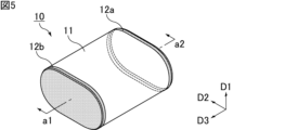
- FIG. 5 is a schematic diagram showing an example of the capacitor element shown in FIGS. 1, 2, 3, and 4 in a perspective view.
- FIG. 6 is a schematic diagram showing an example of a cross section of the capacitor element shown in FIG. 5 along line segment a1-a2.
- FIG. 1 is a schematic diagram showing a perspective view of an example of a capacitor of the present invention.
- FIG. 2 is a schematic diagram showing the capacitor shown in FIG. 1 viewed from a different direction from that shown in FIG.
- FIG. 7 is a schematic diagram showing a perspective view of another example of the capacitor of the present invention.
- FIG. 8 is a schematic diagram showing the capacitor shown in FIG. 7 viewed from the first surface side of the outer case.
- FIG. 9 is a schematic diagram showing a perspective view of an example of the capacitor bank of the present invention.
- FIG. 10 is a schematic diagram showing the capacitor bank shown in FIG. 9 viewed from a different direction from that shown in FIG.
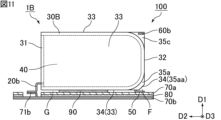
- FIG. 11 is a schematic diagram showing the capacitor bank shown in FIGS. 9 and 10 viewed from the second surface side of the exterior case.
- FIG. 12 is a schematic diagram showing a part of the capacitor bank shown in FIG. 10 in an enlarged view.
- FIG. 13 is a schematic diagram showing a part of the capacitor bank shown in FIG. 12 as viewed from the first surface side of the exterior case.
- the present invention is not limited to the following configuration, and may be modified as appropriate without departing from the gist of the present invention. Furthermore, the present invention also includes a combination of a plurality of individual preferred configurations described below.
- a film capacitor will be shown below as an example of the capacitor of the present invention.
- the capacitor of the present invention is also applicable to capacitors other than film capacitors.
- the capacitor of the present invention includes a capacitor element having an element body and an external electrode provided on an end face of the element body, the capacitor element being electrically connected to the external electrode, and the capacitor element being mounted on an object.
- a pull-out terminal for welding connection an exterior case in which the capacitor element is housed so that the pull-out terminal projects toward the outside, and an outer case filled with the capacitor element so as to be buried therein.
- the outer surface of the outer case includes a mounting surface that faces the mounting object in a first direction when the lead-out terminal is welded and connected to the mounting object; is provided with a mounting mounting leg for welding the exterior case to the mounting object on the mounting surface side, and the mounting mounting leg is electrically insulated from the lead-out terminal, and It is characterized by being made of the same kind of metal material as the lead-out terminal.
- the capacitor exterior case used in the capacitor of the present invention which will be explained below, is also one of the present inventions. That is, the exterior case for a capacitor of the present invention includes a capacitor element having an element body and an external electrode provided on an end face of the element body, the capacitor element being electrically connected to the external electrode, and including the capacitor element.
- An exterior case for a capacitor for storing the capacitor element therein so that the output terminal protrudes outward with respect to an output terminal for welding and connecting the capacitor element to an object to be mounted comprising:
- the outer surface of the outer case includes a mounting surface that faces the mounting object in a first direction when the lead-out terminal is welded to the mounting object, and the outer surface of the outer case includes a mounting surface that faces the mounting object in a first direction when the lead-out terminal is welded to the mounting object. It is characterized in that a mounting mounting leg for welding connection to the mounting object is provided on the side.
- FIG. 1 is a schematic diagram showing a perspective view of an example of the capacitor of the present invention.
- FIG. 2 is a schematic diagram showing the capacitor shown in FIG. 1 viewed from a different direction from that shown in FIG.
- FIG. 3 is a schematic diagram showing the capacitor shown in FIGS. 1 and 2 viewed from a different direction from FIGS. 1 and 2.
- FIG. 4 is a schematic diagram showing the capacitor shown in FIGS. 1, 2, and 3 viewed from the second surface side of the outer case.
- the capacitor 1A shown in FIGS. 1, 2, 3, and 4 includes a capacitor element 10 (see FIG. 5 described later), a first lead terminal 20a, a second lead terminal 20b, and an exterior case 30A. It has a filled resin 40.
- the first direction D1, the second direction D2, and the third direction D3 are orthogonal to each other.
- FIG. 5 is a schematic diagram showing a perspective view of an example of the capacitor element shown in FIGS. 1, 2, 3, and 4.
- FIG. 6 is a schematic diagram showing an example of a cross section of the capacitor element shown in FIG. 5 along line segment a1-a2.
- the capacitor element 10 shown in FIGS. 5 and 6 includes an element body 11, a first external electrode 12a, and a second external electrode 12b.
- the element body 11 is a wound body formed by winding a first metallized film 13a and a second metallized film 13b in a laminated state in the first direction D1. That is, the capacitor 1A, more specifically, the capacitor element 10, is a wound-type film capacitor in which metalized films are laminated and wound.
- the capacitor 1A may be a laminated film capacitor in which metalized films are laminated.
- the cross-sectional shape of the element body 11 is flat when viewed in a cross section perpendicular to the winding axis direction (third direction D3 in FIG. 5). It is preferable. More specifically, it is preferable that the cross-sectional shape of the element body 11 is pressed into a flat shape such as an ellipse or an ellipse, and the thickness is smaller than when the cross-sectional shape of the element body 11 is a perfect circle. .
- the capacitor element 10 may have a cylindrical winding axis.
- the winding axis is arranged on the central axis of the first metallized film 13a and the second metallized film 13b in a wound state, and is used to wind the first metallized film 13a and the second metallized film 13b. This serves as the winding shaft when doing so.
- the first metallized film 13a includes a first dielectric film 14a and a first metal layer 15a.
- the first dielectric film 14a has a first main surface 14aa and a second main surface 14ab that face each other in the first direction D1.
- the first metal layer 15a is provided on the first main surface 14aa of the first dielectric film 14a. More specifically, the first metal layer 15a reaches one side edge of the first dielectric film 14a in the third direction D3 on the first main surface 14aa of the first dielectric film 14a, and extends along the first main surface 14aa of the first dielectric film 14a. It is provided so as not to reach the other side edge of the dielectric film 14a.
- the second metallized film 13b includes a second dielectric film 14b and a second metal layer 15b.
- the second dielectric film 14b has a first main surface 14ba and a second main surface 14bb that face each other in the first direction D1.
- the second metal layer 15b is provided on the first main surface 14ba of the second dielectric film 14b. More specifically, the second metal layer 15b does not reach one side edge of the second dielectric film 14b in the third direction D3 on the first main surface 14ba of the second dielectric film 14b, It is provided so as to reach the other side edge of the second dielectric film 14b.
- the end of the first metal layer 15a that reaches the side edge of the first dielectric film 14a is exposed on one end surface of the element body 11, and the second dielectric layer in the second metal layer 15b
- the adjacent first metallized film 13a and second metallized film 13b are shifted in the third direction D3 so that the end reaching the side edge of the film 14b is exposed to the other end surface of the element body 11.
- the first metallized film 13a protrudes toward the first external electrode 12a with respect to the second metallized film 13b.
- the second metallized film 13b projects toward the second external electrode 12b with respect to the first metallized film 13a.
- the first metal layer 15a is connected to the first external electrode 12a and not connected to the second external electrode 12b.
- the second metal layer 15b is connected to the second external electrode 12b and not connected to the first external electrode 12a.
- the adjacent first metallized film 13a and the second metallized film 13b are shifted in the third direction D3 as described above, the adjacent first dielectric film 14a and the second dielectric film 14b, the first dielectric film 14a in which the first metal layer 15a is provided on the first main surface 14aa is different from the second dielectric film 14b in which the first metal layer 15a is not provided on the main surface. and protrudes toward the first external electrode 12a.
- the second dielectric film 14b in which the second metal layer 15b is provided on the first main surface 14ba has the second metal layer 15b on the first main surface 14ba. It protrudes toward the second external electrode 12b with respect to the first dielectric film 14a that is not provided on the main surface.
- the element body 11 is formed by winding the first metallized film 13a and the second metallized film 13b in a laminated state in the first direction D1, the first dielectric film 14a and the first metal layer 15a , the second dielectric film 14b, and the second metal layer 15b in order in the first direction D1. Moreover, the element body 11 is wound in a state in which the first dielectric film 14a, the first metal layer 15a, the second dielectric film 14b, and the second metal layer 15b are laminated in order in the first direction D1. It can also be said that it is a rolled body.
- the first main surface 14aa of the first dielectric film 14a and the second main surface 14bb of the second dielectric film 14b face each other in the first direction D1
- the second main surface 14ab and the first main surface 14ba of the second dielectric film 14b face each other in the first direction D1.
- the first metallized film 13a and the second metallized film 13b are wound in a laminated state in the first direction D1.
- the second metallized film 13b is inside the first metallized film 13a, and more specifically, the first metal layer 15a is inside the first dielectric film 14a, and The first metallized film 13a and the second metallized film 13b are laminated and wound in the first direction D1 so that the second metal layer 15b is located inside the second dielectric film 14b. That is, in the element body 11, the first metal layer 15a and the second metal layer 15b face each other with the first dielectric film 14a or the second dielectric film 14b in between.
- a fuse portion may be provided in the first metal layer 15a.
- the fuse portion provided in the first metal layer 15a includes, for example, a divided electrode portion in which a portion of the first metal layer 15a that faces the second metal layer 15b is divided into a plurality of parts, and a portion that does not face the second metal layer 15b. This is the part that connects the electrode section.
- Examples of the electrode pattern of the first metal layer 15a provided with the fuse portion include the electrode patterns disclosed in JP-A-2004-363431, JP-A-5-251266, and the like.
- the second metal layer 15b may also be provided with a fuse portion.
- the first dielectric film 14a may contain a curable resin as a main component.
- the main component means the component with the highest weight percentage, preferably the component with the weight percentage higher than 50% by weight.
- the curable resin may be a thermosetting resin or a photocurable resin.
- thermosetting resin means a resin that can be cured by heat, but the curing method thereof is not limited. Therefore, thermosetting resins include resins that can be cured by methods other than heat (eg, light, electron beam, etc.) as long as they can be cured by heat. Further, depending on the material, a reaction may start due to the reactivity of the material itself, and a resin that hardens even without necessarily applying heat or the like from the outside is also referred to as a thermosetting resin. The same applies to photocurable resins, and as long as the resins can be cured by light, resins that can be cured by methods other than light (for example, heat, etc.) are also included.
- the curable resin is preferably made of a cured product of a first organic material having a hydroxyl group (OH group) and a second organic material having an isocyanate group (NCO group).
- the curable resin is a cured product having urethane bonds obtained by the reaction of the hydroxyl groups of the first organic material and the isocyanate groups of the second organic material.
- FT-IR Fourier transform infrared spectrophotometer
- the first dielectric film 14a may contain at least one of a hydroxyl group and an isocyanate group.
- the first dielectric film 14a may contain one of a hydroxyl group and an isocyanate group, or may contain both a hydroxyl group and an isocyanate group.
- Examples of the first organic material include phenoxy resin, polyvinyl acetoacetal resin, polyvinyl butyral resin, and the like.
- the first organic material multiple types of organic materials may be used together.
- the second organic material examples include aromatic polyisocyanates such as diphenylmethane diisocyanate (MDI) and tolylene diisocyanate (TDI), and aliphatic polyisocyanates such as hexamethylene diisocyanate (HDI).
- aromatic polyisocyanates such as diphenylmethane diisocyanate (MDI) and tolylene diisocyanate (TDI)
- aliphatic polyisocyanates such as hexamethylene diisocyanate (HDI).
- HDI hexamethylene diisocyanate
- the second organic material multiple types of organic materials may be used together.
- the first dielectric film 14a may contain thermoplastic resin as a main component.
- thermoplastic resin examples include polypropylene, polyether sulfone, polyetherimide, polyarylate, and the like.
- the first dielectric film 14a may contain additives for adding various functions.
- additives include leveling agents for imparting smoothness.
- the additive preferably has a functional group that reacts with a hydroxyl group and/or an isocyanate group and forms a part of the crosslinked structure of the cured product.
- examples of such additives include resins having at least one functional group selected from the group consisting of hydroxyl groups, epoxy groups, silanol groups, and carboxyl groups.
- the second dielectric film 14b may also contain a curable resin as a main component, or may contain a thermoplastic resin as a main component. Further, the second dielectric film 14b may also contain additives, similar to the first dielectric film 14a.
- compositions of the first dielectric film 14a and the second dielectric film 14b may be different from each other, but are preferably the same.
- the thickness of the first dielectric film 14a and the second dielectric film 14b is preferably 1 ⁇ m or more and 10 ⁇ m or less, more preferably 3 ⁇ m or more and 5 ⁇ m or less.
- the thicknesses of the first dielectric film 14a and the second dielectric film 14b may be different from each other, but are preferably the same.
- the thickness of the dielectric film is measured using an optical film thickness meter.
- the first dielectric film 14a and the second dielectric film 14b are each preferably produced by molding a resin solution containing the above-mentioned resin material into a film shape and then curing it by heat treatment.
- Examples of the constituent materials of the first metal layer 15a and the second metal layer 15b include metals such as aluminum, zinc, titanium, magnesium, tin, and nickel.
- compositions of the first metal layer 15a and the second metal layer 15b may be different from each other, but are preferably the same.
- the thickness of the first metal layer 15a and the second metal layer 15b is preferably 5 nm or more and 40 nm or less.
- the thicknesses of the first metal layer 15a and the second metal layer 15b may be different from each other, but are preferably the same.
- the thickness of the metal layer is measured by observing a cross section of the metallized film along the first direction using a transmission electron microscope (TEM).
- TEM transmission electron microscope
- the first metal layer 15a and the second metal layer 15b are each preferably formed by depositing the metal as described above on the main surfaces of the first dielectric film 14a and the second dielectric film 14b.
- the first external electrode 12a is provided on one end surface of the element body 11. More specifically, the first external electrode 12a is connected to the first metal layer 15a by contacting the end of the first metal layer 15a exposed on one end surface of the element body 11. On the other hand, the first external electrode 12a is not connected to the second metal layer 15b.
- the second external electrode 12b is provided on the other end surface of the element body 11. More specifically, the second external electrode 12b is connected to the second metal layer 15b by contacting the end of the second metal layer 15b exposed on the other end surface of the element body 11. On the other hand, the second external electrode 12b is not connected to the first metal layer 15a.
- Examples of the constituent material of the first external electrode 12a and the second external electrode 12b include metals such as zinc, aluminum, tin, and zinc-aluminum alloy.
- compositions of the first external electrode 12a and the second external electrode 12b may be different from each other, but are preferably the same.
- the first external electrode 12a and the second external electrode 12b are preferably formed by spraying the metal as described above onto one end surface and the other end surface of the element body 11, respectively.
- the first lead terminal 20a is electrically connected to the first external electrode 12a (see FIGS. 5 and 6).
- the first lead terminal 20a is electrically connected to the first external electrode 12a via a joining member such as solder.
- the second lead terminal 20b is electrically connected to the second external electrode 12b (see FIGS. 5 and 6).
- the second lead terminal 20b is electrically connected to the second external electrode 12b via a joining member such as solder.
- the first lead-out terminal 20a and the second lead-out terminal 20b are lead-out terminals for welding and connecting the capacitor element 10 to the mounting target, respectively.
- the capacitor 1A When mounting the capacitor 1A on an object to be mounted, in order to connect the first drawer terminal 20a and the second drawer terminal 20b to the object to be mounted by welding, the first drawer terminal 20a and the second drawer terminal 20b are fastened with screws,
- the capacitor 1A, especially the capacitor element 10 can be firmly fixed to the mounting object compared to the case where it is fixed to the mounting object by soldering or the like. Thereby, the vibration and shock resistance of the capacitor 1A mounted on the object can be improved.
- the first lead-out terminal 20a and the second lead-out terminal 20b are welded and connected to the mounting target, so that the connection between the first lead-out terminal 20a and the mounting target is The resistance and the connection resistance between the second lead-out terminal 20b and the mounting object can be reduced. Thereby, the conductivity between the capacitor 1A and the object to be mounted can be improved.
- the shapes of the first pull-out terminal 20a and the second pull-out terminal 20b may each be, for example, plate-shaped or linear (rod-shaped). In this case, each of the first extraction terminal 20a and the second extraction terminal 20b may have a partially bent shape.
- the capacitor element 10 (see FIGS. 5 and 6) is housed inside the exterior case 30A so that the first pull-out terminal 20a and the second pull-out terminal 20b protrude toward the outside. Although not shown in FIG. 1 etc., it is preferable that the capacitor element 10 is housed in the center of the interior of the exterior case 30A while being separated from the inner surface of the exterior case 30A.
- the shape of the exterior case 30A is, for example, a bottomed cylindrical shape with an opening 31 provided at one end in the second direction D2, as shown in FIG. 1 and the like.
- the outer surface of the exterior case 30A includes a first surface 32 facing the opening 31 in the second direction D2, and a second surface extending from the first surface 32 toward the opening 31 in the second direction D2. 33 (including four surfaces in the example shown in FIG. 1 etc.).
- Examples of the exterior case 30A include a resin case, a metal case, and the like.
- the exterior case 30A is a resin case
- the resin constituting the resin case examples include liquid crystal polymer (LCP), polyphenylene sulfide, polybutylene terephthalate, and the like.
- LCP liquid crystal polymer
- the resin case contains a liquid crystal polymer.
- liquid crystal polymer contained in the resin case for example, a liquid crystal polymer having p-hydroxybenzoic acid and 6-hydroxy-2-naphthoic acid groups in its skeleton is used. Furthermore, in addition to p-hydroxybenzoic acid and 6-hydroxy-2-naphthoic acid groups, liquid crystal polymers formed into polycondensates using various components such as phenol, phthalic acid, and ethylene terephthalate can be used. Further, when classifying liquid crystal polymers, there are classification methods such as type I, type II, and type III, but the material means the same material as the liquid crystal polymer formed from the above-mentioned components.
- the resin case further contains an inorganic filler in addition to the liquid crystal polymer.
- the inorganic filler contained in the resin case a material with higher strength than liquid crystal polymer can be used.
- the inorganic filler is preferably a material with a melting point higher than that of the liquid crystal polymer, and more preferably a material with a melting point of 680° C. or higher.
- the form of the inorganic filler is not particularly limited, and examples thereof include forms having a longitudinal direction such as fibrous or plate-like forms. As such a form of inorganic filler, a plurality of types of inorganic materials may be used together. It is preferable that the resin case contains at least one of a fibrous inorganic material and a plate-like inorganic material as an inorganic filler.
- the term ⁇ the filler is fibrous'' means that in the filler, the relationship between the longitudinal dimension and the cross-sectional diameter in a cross section perpendicular to the longitudinal direction is 5 (i.e., aspect ratio). means a state in which the ratio is 5:1 or more).
- the cross-sectional diameter is the longest distance between two points on the outer circumference of the cross-section. If the cross-sectional diameter differs in the longitudinal direction, measure at the point where the cross-sectional diameter is maximum.
- the cross-sectional diameter/maximum height when the filling material is plate-shaped, the relationship between the cross-sectional diameter of the surface with the largest projected area and the maximum height in the direction orthogonal to this cross-section is defined as the cross-sectional diameter/maximum height. It means a state in which the value is 3.
- At least a portion of the inorganic filler is oriented toward the second surface 33 of the outer case 30A, in a portion oriented from the first surface 32 toward the opening 31 and toward the adjacent second surface 33. It is preferable that the outer case 30A has a plurality of portions and is dispersed inside the outer case 30A.
- the size of the inorganic filler is preferably 5 ⁇ m or more in diameter and 50 ⁇ m or more in length.
- the inorganic filler is dispersed throughout the exterior case 30A without agglomerating.
- the inorganic filler examples include inorganic materials such as fibrous glass filler, plate-shaped talc, or mica. Among these, it is preferable that the inorganic filler contains fibrous glass filler as a main component.
- the resin case contains another resin (for example, polyphenylene sulfide) instead of the liquid crystal polymer, it is preferable that the resin case further contains an inorganic filler as described above.
- another resin for example, polyphenylene sulfide
- the resin case further contains an inorganic filler as described above.
- the resin case is manufactured, for example, by a method such as injection molding.
- the exterior case 30A is a metal case
- the metal constituting the metal case include simple metals such as aluminum, magnesium, iron, stainless steel, and copper, and alloys containing at least one of these simple metals. It will be done. Among these, it is preferable that the metal case contains aluminum or an aluminum alloy.
- the metal case is manufactured, for example, by a method such as impact molding.
- one capacitor element 10 is housed inside one exterior case 30A, but a plurality of capacitor elements 10 are housed inside one exterior case 30A. Good too.
- the filling resin 40 is filled in the exterior case 30A so as to bury the capacitor element 10. By being filled with the filling resin 40 in this manner, the capacitor element 10 is held inside the exterior case 30A.
- the filling resin 40 is placed between the capacitor element 10 and the outer case 30A, more specifically, between the capacitor element 10 and the outer case 30A. is filled between the outer surface of the outer case 30A and the inner surface of the outer case 30A. Further, the filling resin 40 is filled inside the exterior case 30A, not only between the capacitor element 10 and the exterior case 30A, but also in a region extending from the opening 31 of the exterior case 30A to the capacitor element 10.
- the filling resin 40 from the viewpoint of suppressing the infiltration of moisture into the capacitor element 10, it is preferable to appropriately select a resin with low moisture permeability, and examples thereof include epoxy resin, silicone resin, urethane resin, and the like.
- examples of curing agents for epoxy resins include amine curing agents and imidazole curing agents.
- the filling resin 40 only the resin mentioned above may be used, but a reinforcing agent may be added to the resin for the purpose of improving the strength.
- a reinforcing agent include silica and alumina.
- the thickness of the filling resin 40 in the opening 31 of the outer case 30A is large.
- the thickness of the filling resin 40 in the opening 31 of the outer case 30A is preferably large enough within the allowable range of the entire volume (physique) of the capacitor 1A, specifically, preferably 2 mm or more, more preferably 4 mm or more. be.
- the thickness of the filling resin 40 to the capacitor element 10 can be reduced by the opening 31 of the outer case 30A. It is preferable to make it larger on the side than on the first surface 32 side.
- the thickness of the filled resin 40 is measured using a soft X-ray device if it is in a non-destructive state, and is measured using a length measuring device such as a caliper if it is in a destructive state.
- the relationship between the height of the outer case 30A and the height of the filled resin 40 in the second direction D2 is such that the thickness of the filled resin 40 at the opening 31 of the outer case 30A is made as large as possible, and the position inside the outer case 30A is It may be up to a maximum, it may be about a full cup, or it may be slightly overflowing due to surface tension.
- the outer surface of the exterior case 30A includes a mounting surface 34 that faces the mounting target in the first direction D1 when the first pull-out terminal 20a and the second pull-out terminal 20b are welded and connected to the mounting target.
- the outer surface of the exterior case 30A includes a mounting surface 34 as a part of the second surface 33.
- Mounting mounting legs 50 are provided on the outer surface of the exterior case 30A.
- the mounting mounting leg 50 is attached to the first rib 35a provided on the outer surface of the exterior case 30A, here the mounting surface 34 (second surface 33). In this way, in the example shown in FIG. 1 and the like, mounting mounting legs 50 are provided on the mounting surface 34 of the exterior case 30A.
- the mounting mounting leg 50 is attached to the first rib 35a by, for example, insert molding or the like.
- the shape of the first rib 35a is not particularly limited.
- first rib 35a may not be provided on the outer surface of the exterior case 30A. That is, the location where the mounting mounting leg 50 is provided is not limited to the first rib 35a of the exterior case 30A.
- the mounting mounting leg 50 is a mounting leg for welding the exterior case 30A to the mounting target on the mounting surface 34 side.
- the mounting mounting legs 50 When mounting the capacitor 1A on the mounting object, the mounting mounting legs 50 are welded and connected to the mounting object, so there are cases where the mounting mounting legs 50 are fixed to the mounting object by screwing, soldering, etc.
- the capacitor 1A, especially the outer case 30A can be firmly fixed to the mounting target. Thereby, the vibration and shock resistance of the capacitor 1A mounted on the object can be improved.
- the mounting mounting legs 50 are attached to the mounting object in the same process as welding and connecting the first extraction terminal 20a and the second extraction terminal 20b to the mounting object. Can be connected by welding.
- the conventional fixing process such as fixing the capacitor to the mounting target by screwing etc. is not necessary, which is necessary for fixing the capacitor to the mounting target. Time, cost, etc. can be reduced.
- the mounting mounting leg 50 is electrically insulated from the first extraction terminal 20a and the second extraction terminal 20b. That is, in the capacitor 1A, the mounting mounting leg 50 is electrically insulated from the capacitor element 10 to which the first extraction terminal 20a and the second extraction terminal 20b are electrically connected.
- the mounting mounting leg 50 is made of the same kind of metal material as the first pull-out terminal 20a and the second pull-out terminal 20b. Thereby, when mounting the capacitor 1A on the mounting object, the mounting mounting leg 50 can be welded and connected to the mounting object using the same welding method as the first pull-out terminal 20a and the second pull-out terminal 20b.
- the expression that a plurality of members are made of the same type of metal material means that the types of metal elements that are the basic components of the metal materials are the same.
- the basic component of the metal material may be composed of only one type of metal element, or may be composed of multiple types of metal elements.
- the metal elements of the basic components of the metal material constituting one member are E1 and E2
- the basic metallic elements of the metallic material constituting the other member are E1 and E2
- both members are composed of the same kind of metallic material. The same applies when comparing three or more members.
- the content of the basic components in the metal material may be the same, different, or partially different among the plurality of members.
- the weight ratios of the multiple metal elements in the basic component may be the same or different between the multiple members. , may differ in some parts.
- the metal material may also contain 1% by weight or less of additional components.
- the types of metal elements that are additive components of the metal material may be the same, different, or partially different among the plurality of members.
- the additive component of the metal material may be composed of only one type of metal element, or may be composed of multiple types of metal elements.
- the content of the additive component in the metal material may be the same, different, or partially different between the plurality of members.
- the weight ratio of the multiple metal elements in the additive component may be the same or different between the multiple members. , may differ in some parts.
- the metal material does not need to contain any additive components.
- the metal materials of all members may contain the additive component, the metal materials of some members may contain the additive component, or the metal materials of all the members may contain the additive component. It does not have to contain.
- Examples of the metal material constituting the first pull-out terminal 20a, the second pull-out terminal 20b, and the mounting mounting leg 50 include copper, oxygen-free copper, aluminum, and an alloy containing at least one of these. . Among these, it is preferable that the metal material constituting the first lead-out terminal 20a, the second lead-out terminal 20b, and the mounting mounting leg 50 is copper or oxygen-free copper.
- the metal material constituting the first extraction terminal 20a, the second extraction terminal 20b, and the mounting mounting leg 50 is a copper-based material, for example, oxygen-free copper (copper: 99.96% by weight or more), tough pitch copper (copper: 99.90% by weight or more), phosphorus deoxidized copper (copper: 99.90% by weight or more, phosphorus: 0.015% by weight or more and 0.040% by weight or less), etc. can be used.
- a welding method such as laser welding or resistance welding is used.
- laser welding has the advantage that welding can be performed in a short time by local heating, and welding distortion can be reduced.
- the mounting mounting legs 50 protrude beyond the mounting surface 34 of the exterior case 30A in the first direction D1.
- a gap can be provided between the mounting surface 34 of the outer case 30A and the mounting object while the capacitor 1A is mounted on the mounting object.
- the gap provided between the mounting surface 34 of the outer case 30A and the mounting target is filled with heat dissipation paste, underfill adhesive (e.g. containing epoxy resin). It can be used as a location for connecting members such as adhesives.
- the capacitor 1A can be firmly fixed to the object to be mounted.
- first lead-out terminal 20a and the second lead-out terminal 20b each protrude beyond the mounting surface 34 of the exterior case 30A in the first direction D1.
- the distance between the mounting surface 34 of the outer case 30A and the mounting object is the distance between the first pull-out terminal 20a, the second pull-out terminal 20b, and the mounting mounting leg 50. can be adjusted by the shape of the
- a space F is provided between the mounting surface 34 of the exterior case 30A and the mounting mounting leg 50.
- a space F is provided between the first surface 35aa of the first rib 35a included in the mounting surface 34 of the exterior case 30A and the mounting mounting leg 50.
- a laser beam is irradiated to the welding part of the mounting mounting leg 50 during laser welding, or an electrode is used during resistance welding. Welding work such as contacting the mounting mounting leg 50 becomes easier.
- the distance between the mounting surface 34 of the exterior case 30A and the mounting mounting leg 50 can be adjusted depending on the shape of the mounting mounting leg 50.
- the space F does not need to be provided between the mounting surface 34 of the exterior case 30A and the mounting mounting leg 50.
- the mounting legs 50 for mounting may be provided along the mounting surface 34 of the outer case 30A so as to be in contact with the mounting surface 34 of the outer case 30A.
- the mounting mounting legs 50 do not protrude from the exterior case 30A when viewed from the first direction D1.
- the mounting mounting legs 50 for mounting do not protrude from the outer case 30A
- the mounting area of the capacitor 1A is Can be reduced.
- the mounting mounting legs 50 do not protrude from the exterior case 30A when viewed from the first direction D1 compared to the case where the mounting mounting legs 50 protrude from the exterior case 30A, for example, a plurality of When the capacitors 1A are arranged and mechanically connected in a direction perpendicular to the first direction D1 (in the example shown in FIG. 1, a direction including the second direction D2 and the third direction D3), adjacent capacitors 1A are Less likely to interfere.
- the mounting mounting legs 50 may protrude from the exterior case 30A when viewed from the first direction D1. In this case, since the part of the mounting leg 50 protruding from the outer case 30A can be used as a welding part, there is no space between the mounting surface 34 of the outer case 30A and the mounting leg 50. It's okay.
- the shape of the mounting mounting leg 50 may be, for example, plate-like or linear (rod-like). In this case, the mounting mounting leg 50 may have a partially bent shape.
- Only one mounting mounting leg 50 may be provided as shown in FIG. 1, etc., or a plurality of mounting mounting legs 50 may be provided.
- FIG. 7 is a schematic diagram showing a perspective view of another example of the capacitor of the present invention.
- FIG. 8 is a schematic diagram showing the capacitor shown in FIG. 7 viewed from the first surface side of the outer case.
- the capacitor 1B shown in FIGS. 7 and 8 has an outer case 30B instead of the outer case 30A, unlike the capacitor 1A shown in FIG. 1, etc.
- a first fixing mounting leg 60a and a second fixing mounting leg 60b are further provided on the outer surface of the exterior case 30B.
- the first fixing mounting leg 60a is attached to the second rib 35b provided on the outer surface of the exterior case 30B, here the second surface 33.
- the first fixing mounting leg 60a is attached to the second rib 35b, for example, by a method such as insert molding.
- the second fixing mounting leg 60b is attached to the third rib 35c provided on the outer surface of the exterior case 30B, here the second surface 33.
- the second fixing mounting leg 60b is attached to the third rib 35c, for example, by a method such as insert molding.
- the shapes of the second rib 35b and the third rib 35c are not particularly limited.
- the second rib 35b and the third rib 35c may not be provided on the outer surface of the exterior case 30B. That is, the location where the fixing mounting leg 60 is provided is not limited to the second rib 35b and the third rib 35c of the exterior case 30B.
- the first fixing mounting leg 60a and the second fixing mounting leg 60b are mounting legs for welding and connecting the exterior case 30B to another exterior case.
- the first fixing mounting leg 60a is provided at a different position from the mounting mounting leg 50 so as to be electrically insulated from the first extraction terminal 20a and the second extraction terminal 20b. That is, the first fixing mounting leg 60a is electrically insulated from the capacitor element 10 to which the first extraction terminal 20a and the second extraction terminal 20b are electrically connected.
- the second fixing mounting leg 60b is provided at a different position from the mounting mounting leg 50 so as to be electrically insulated from the first extraction terminal 20a and the second extraction terminal 20b.
- the second fixing mounting leg 60b is electrically insulated from the capacitor element 10 to which the first extraction terminal 20a and the second extraction terminal 20b are electrically connected.
- first fixing mounting leg 60a and the second fixing mounting leg 60b are electrically insulated from each other.
- first fixing mounting leg 60a and the second fixing mounting leg 60b are each electrically insulated from the mounting mounting leg 50.
- first fixing mounting leg 60a and the second fixing mounting leg 60b are made of the same kind of metal material as the first pull-out terminal 20a and the second pull-out terminal 20b. That is, it is preferable that the first fixing mounting leg 60a and the second fixing mounting leg 60b are made of the same type of metal material as the mounting mounting leg 50. In this case, the first fixing mounting leg 60a and the second fixing mounting leg 60a are attached using the same welding method used when welding the first pull-out terminal 20a, the second pull-out terminal 20b, and the mounting mounting leg 50 to the mounting object. It can be connected to the leg 60b by welding.
- Examples of the metal material constituting the first fixing mounting leg 60a and the second fixing mounting leg 60b include copper, oxygen-free copper, aluminum, and an alloy containing at least one of these. Among these, it is preferable that the metal material forming the first fixing mounting leg 60a and the second fixing mounting leg 60b is copper or oxygen-free copper.
- the metal material constituting the first fixing mounting leg 60a and the second fixing mounting leg 60b is a copper-based material
- oxygen-free copper copper: 99.96% by weight or more
- tough pitch copper copper: 99.9% by weight or more
- .90% by weight or more phosphorus deoxidized copper
- phosphorus: 0.015% by weight or more, 0.040% by weight or less etc.
- a welding method such as laser welding or resistance welding is used.
- the mounting mounting leg 50 and the first fixing mounting leg 60a are preferably provided at different height positions in the first direction D1. Further, as shown in FIG. 7 and the like, the mounting mounting leg 50 and the second fixing mounting leg 60b are preferably provided at different height positions in the first direction D1.
- each capacitor 1B when a plurality of capacitors 1B are mechanically connected and mounted on a mounting target, each capacitor 1B, especially each outer case 30B, can be fixed at multiple locations at different height positions. The vibration and shock resistance can be sufficiently improved when the capacitor 1B is mechanically connected.
- the first fixing mounting leg 60a and the second fixing mounting leg 60b may be provided at the same height position in the first direction D1, or may be provided at different height positions in the first direction D1. It's okay.
- first fixing mounting leg 60a and the second fixing mounting leg 60b are provided at different height positions in the first direction D1, as shown in FIG. 13 described later, the first fixing mounting leg 60a
- the surfaces of the second fixing mounting legs 60b facing each other in the first direction D1 can be easily welded and connected to each other.
- the mounting mounting leg 50 and the first fixing mounting leg 60a extend in mutually different directions. Furthermore, as shown in FIG. 7 etc., it is preferable that the mounting mounting leg 50 and the second fixing mounting leg 60b extend in mutually different directions. In this case, it becomes easier to weld and connect the first fixing attaching leg 60a and the second fixing attaching leg 60b while welding the mounting attaching leg 50 to the mounting target.
- the mounting mounting legs 50 for mounting and the first mounting legs 60a for fixing extend in different directions
- the mounting mounting legs 50 for mounting and the first mounting legs 60a for fixing extend in directions that are orthogonal to the first direction D1 and intersect with each other. It may extend to Furthermore, when the mounting mounting legs 50 for mounting and the second mounting legs 60b for fixing extend in different directions, the mounting mounting legs 50 for mounting and the second mounting legs 60b for fixing cross each other while being perpendicular to the first direction D1. It may extend in the direction.
- the mounting mounting leg 50 may extend in the second direction D2
- the first fixing mounting leg 60a and the second fixing mounting leg 60b may extend in the third direction D3.
- the mounting mounting legs 50 are welded and connected to the mounting object, and the first fixing mounting legs 60a and the second fixing mounting legs 60b are connected. Easier to weld connections.
- mounting mounting leg 50 and the first fixing mounting leg 60a do not have to extend in directions perpendicular to each other. Further, the mounting mounting leg 50 and the second fixing mounting leg 60b do not need to extend in directions perpendicular to each other.
- first fixing mounting leg 60a and the second fixing mounting leg 60b may be, for example, plate-shaped or linear (rod-shaped). In this case, each of the first fixing mounting leg 60a and the second fixing mounting leg 60b may have a partially bent shape.
- Only one first fixing mounting leg 60a and second fixing mounting leg 60b may be provided, as shown in FIG. 7, etc., or a plurality of them may be provided.
- the capacitor bank of the present invention is characterized by comprising the capacitor of the present invention, and the mounting object to which the lead-out terminal and mounting leg of the capacitor are welded and connected.
- FIG. 9 is a schematic diagram showing a perspective view of an example of the capacitor bank of the present invention.
- FIG. 10 is a schematic diagram showing the capacitor bank shown in FIG. 9 viewed from a different direction from that shown in FIG.
- FIG. 11 is a schematic diagram showing the capacitor bank shown in FIGS. 9 and 10 viewed from the second surface side of the exterior case.
- the capacitor bank 100 shown in FIGS. 9, 10, and 11 includes a plurality of capacitors 1B (see FIGS. 7 and 8), a first bus bar 70a, and a second bus bar 70b.
- the first bus bar 70a and the second bus bar 70b are included in a mounting object on which a plurality of capacitors 1B are mounted.
- the first bus bar 70a and the second bus bar 70b are stacked in the first direction D1. More specifically, the first bus bar 70a is provided closer to the capacitor 1B than the second bus bar 70b in the first direction D1. In other words, the second bus bar 70b is provided on the opposite side of the capacitor 1B from the first bus bar 70a in the first direction D1.
- Examples of the constituent material of the first bus bar 70a and the second bus bar 70b include metals such as copper.
- An insulating member 80 is provided between the first bus bar 70a and the second bus bar 70b to ensure insulation between them.
- Examples of the constituent material of the insulating member 80 include resin.
- the first bus bar 70a and the insulating member 80 are both hollowed out in some areas.
- the second bus bar 70b is exposed from the first bus bar 70a and the insulating member 80 as an exposed portion 71b.
- the plurality of capacitors 1B are each mounted on the mounting object including the first bus bar 70a and the second bus bar 70b on the mounting surface 34 side of the outer case 30B. More specifically, it is as follows.
- the first lead terminal 20a is welded to the first bus bar 70a, and the second lead terminal 20b is connected to the second bus bar 70b, here, the second bus bar 70b. It is welded and connected to the exposed portion 71b.
- the mounting mounting leg 50 is welded and connected to the first bus bar 70a. In the state of the capacitor 1B alone, the mounting mounting leg 50 is electrically insulated from the first lead-out terminal 20a, but in the state of the capacitor bank 100, the mounting mounting leg 50 is electrically insulated from the first lead-out terminal 20a through the first bus bar 70a. It will be electrically connected to the first extraction terminal 20a.
- each capacitor 1B is connected to the mounting target including the first bus bar 70a and the second bus bar 70b. is welded to the Therefore, in the capacitor bank 100, each capacitor 1B is firmly fixed to the mounting target. This improves the vibration and shock resistance of the capacitor bank 100 in which a plurality of capacitors 1B are mounted on an object.
- the capacitor bank 100 having the above-described configuration can be manufactured at low cost.
- the first lead-out terminal 20a, the second lead-out terminal 20b, and the mounting mounting leg 50 of each capacitor 1B are connected to the mounting surface 30 of the exterior case 30B in the first direction D1. It is preferable that it protrude more than that.
- a gap G is provided between the mounting surface 34 of the exterior case 30B of each capacitor 1B and the mounting target, here the first bus bar 70a.
- the connection member 90 is preferably provided in the gap G so as to be in contact with the mounting surface 34 of the exterior case 30B of each capacitor 1B and the first bus bar 70a. .
- each capacitor 1B and the first bus bar 70a are also connected via the connecting member 90.
- a heat dissipation paste is used as the connection member 90, it becomes easy to achieve the desired heat dissipation performance of each capacitor 1B.
- an underfill adhesive is used as the connecting member 90, each capacitor 1B, particularly the outer case 30B of each capacitor 1B, can be fixed sufficiently firmly to the first bus bar 70a.
- the plurality of capacitors 1B are mechanically connected. More specifically, it is as follows.
- FIG. 12 is a schematic diagram showing an enlarged view of a part of the capacitor bank shown in FIG. 10.
- FIG. 13 is a schematic diagram showing a part of the capacitor bank shown in FIG. 12 as viewed from the first surface side of the exterior case.
- the first fixing mounting leg 60a of one capacitor 1B and the second fixing mounting leg 60b of the other capacitor 1B are welded. It is connected.
- the first fixing mounting leg 60a and the second fixing mounting leg 60b are provided at different height positions in the first direction D1. The surfaces of the leg 60a and the second fixing mounting leg 60b that face each other in the first direction D1 are welded together.
- adjacent capacitors 1B are welded and connected via the first fixing mounting leg 60a and the second fixing mounting leg 60b. Therefore, in the capacitor bank 100, adjacent capacitors 1B are firmly connected to each other, especially adjacent exterior cases 30B are firmly connected to each other. Thereby, in the capacitor bank 100, the vibration and shock resistance is improved in a state where the plurality of capacitors 1B are mechanically connected.
- the first fixing mounting leg 60a and the second fixing mounting leg 60b are provided at different height positions from the mounting mounting leg 50 in the first direction D1. It is preferable.
- each capacitor 1B, especially each exterior case 30B is fixed at multiple locations at different heights, so the durability of the multiple capacitors 1B in a mechanically connected state is limited. Vibration and impact resistance is sufficiently improved.
- the mounting mounting leg 50 and the first fixing mounting leg 60a preferably extend in different directions. Furthermore, as shown in FIG. 12, in the capacitor bank 100, it is preferable that the mounting mounting leg 50 and the second fixing mounting leg 60b extend in mutually different directions. In this case, when manufacturing the capacitor bank 100, it becomes easier to weld and connect the first fixing attaching leg 60a and the second fixing attaching leg 60b while welding the mounting attaching leg 50 to the first bus bar 70a. .
- the mounting mounting legs 50 extend in the second direction D2, and the first fixing mounting legs 60a and the second fixing mounting legs 60b extend in the third direction D3. good.
- the mounting mounting legs 50 are welded and connected to the mounting object, and the first fixing mounting legs 60a and It becomes easier to weld and connect the second fixing mounting leg 60b.
- the capacitor bank 100 has a plurality of capacitors 1B, the number of capacitors 1B that the capacitor bank 100 has is not limited to six as shown in FIG. 9 and the like.
- the capacitor bank 100 has a plurality of capacitors 1B, it may have only one capacitor 1B.
- capacitor bank 100 all of the plurality of capacitors 1B may be replaced with capacitors 1A (see FIGS. 1, 2, 3, and 4), or some of them may be replaced with capacitors 1A. It's okay.
- bus bars such as the first bus bar 70a and the second bus bar 70b are used as mounting objects, but in addition to bus bars, substrates, casings, etc. may be used as mounting objects.
- the capacitor of the present invention can improve vibration and shock resistance when mounted on an object, it is useful as a smoothing capacitor for automotive applications that particularly requires high vibration and shock resistance.
- the capacitor bank of the present invention can improve vibration and shock resistance when the capacitor of the present invention is mounted on an object, so the capacitor bank of the present invention can improve vibration and shock resistance when the capacitor of the present invention is mounted on an object. , inverters).
- a capacitor element having an element body and an external electrode provided on an end surface of the element body; a lead-out terminal electrically connected to the external electrode and for welding the capacitor element to the mounting target; an exterior case in which the capacitor element is housed so that the extraction terminal protrudes toward the outside; a filled resin filled in the outer case so as to embed the capacitor element;
- the outer surface of the exterior case includes a mounting surface that faces the mounting object in a first direction when the lead-out terminal is welded and connected to the mounting object,
- the outer surface of the outer case is provided with mounting mounting legs for welding the outer case to the mounting object on the mounting surface side,
- a capacitor characterized in that the mounting mounting leg is electrically insulated from the lead-out terminal and made of the same type of metal material as the lead-out terminal.
- ⁇ 3> The capacitor according to ⁇ 2>, wherein a space is provided between the mounting surface of the exterior case and the mounting mounting leg.
- ⁇ 4> The capacitor according to any one of ⁇ 1> to ⁇ 3>, wherein the mounting mounting leg does not protrude from the outer case when viewed from the first direction.
- fixing mounting legs for welding the exterior case to another exterior case are located at different positions from the mounting legs so that the mounting legs are electrically insulated from the lead-out terminals.
- ⁇ 6> The capacitor according to ⁇ 5>, wherein the mounting leg and the fixing leg are provided at different height positions in the first direction.
- the mounting mounting leg extends in a second direction perpendicular to the first direction,
- a capacitor bank comprising: the mounting object to which the extraction terminal of the capacitor and the mounting mounting leg are welded and connected.
- a capacitor element having an element body and an external electrode provided on an end face of the element body, and a drawer electrically connected to the external electrode and for welding the capacitor element to a mounting target.
- An exterior case for a capacitor for accommodating the capacitor element therein so that the lead-out terminal protrudes outward with respect to the terminal,
- the outer surface of the exterior case includes a mounting surface that faces the mounting object in a first direction when the lead-out terminal is welded and connected to the mounting object,
- An exterior case for a capacitor characterized in that the exterior case is provided with mounting mounting legs on the exterior surface thereof for welding and connecting the exterior case to the mounting object on the mounting surface side.
Landscapes
- Engineering & Computer Science (AREA)
- Power Engineering (AREA)
- Microelectronics & Electronic Packaging (AREA)
- Manufacturing & Machinery (AREA)
- Fixed Capacitors And Capacitor Manufacturing Machines (AREA)
Priority Applications (3)
| Application Number | Priority Date | Filing Date | Title |
|---|---|---|---|
| CN202380046479.XA CN119301713A (zh) | 2022-06-17 | 2023-04-25 | 电容器、电容器组以及电容器用外装壳体 |
| JP2024528350A JP7794316B2 (ja) | 2022-06-17 | 2023-04-25 | コンデンサ、コンデンサバンク、及び、コンデンサ用外装ケース |
| US18/976,695 US20250104912A1 (en) | 2022-06-17 | 2024-12-11 | Capacitor, capacitor bank, and outer case for capacitor |
Applications Claiming Priority (2)
| Application Number | Priority Date | Filing Date | Title |
|---|---|---|---|
| JP2022098188 | 2022-06-17 | ||
| JP2022-098188 | 2022-06-17 |
Related Child Applications (1)
| Application Number | Title | Priority Date | Filing Date |
|---|---|---|---|
| US18/976,695 Continuation US20250104912A1 (en) | 2022-06-17 | 2024-12-11 | Capacitor, capacitor bank, and outer case for capacitor |
Publications (1)
| Publication Number | Publication Date |
|---|---|
| WO2023243233A1 true WO2023243233A1 (ja) | 2023-12-21 |
Family
ID=89190965
Family Applications (1)
| Application Number | Title | Priority Date | Filing Date |
|---|---|---|---|
| PCT/JP2023/016312 Ceased WO2023243233A1 (ja) | 2022-06-17 | 2023-04-25 | コンデンサ、コンデンサバンク、及び、コンデンサ用外装ケース |
Country Status (4)
| Country | Link |
|---|---|
| US (1) | US20250104912A1 (https=) |
| JP (1) | JP7794316B2 (https=) |
| CN (1) | CN119301713A (https=) |
| WO (1) | WO2023243233A1 (https=) |
Cited By (2)
| Publication number | Priority date | Publication date | Assignee | Title |
|---|---|---|---|---|
| WO2025141924A1 (ja) * | 2023-12-26 | 2025-07-03 | 株式会社村田製作所 | コンデンサモジュール |
| DE102024203144A1 (de) * | 2024-04-08 | 2025-10-09 | Zf Friedrichshafen Ag | Zwischenkreiskondensatormodul, Zwischenkreiskondensatoranordnung sowie Stromrichter mit einer derartigen Zwischenkreiskondensatoranordnung |
Citations (5)
| Publication number | Priority date | Publication date | Assignee | Title |
|---|---|---|---|---|
| JP2004165309A (ja) * | 2002-11-12 | 2004-06-10 | Mitsubishi Electric Corp | コンデンサユニット及びこのコンデンサユニットを有する半導体電力変換装置 |
| JP2015035505A (ja) * | 2013-08-09 | 2015-02-19 | 日立エーアイシー株式会社 | 金属化フィルムコンデンサ |
| CN210123694U (zh) * | 2019-07-29 | 2020-03-03 | 六和电子(江西)有限公司 | 一种线路板卧式安装的薄膜电容器塑壳结构 |
| CN211628892U (zh) * | 2020-05-09 | 2020-10-02 | 广东丰明电子科技有限公司 | 一种快速换接安装耳电容器 |
| JP2021153150A (ja) * | 2020-03-24 | 2021-09-30 | パナソニックIpマネジメント株式会社 | コンデンサモジュールおよびコンデンサモジュールの製造方法 |
Family Cites Families (2)
| Publication number | Priority date | Publication date | Assignee | Title |
|---|---|---|---|---|
| JP3729678B2 (ja) * | 1999-04-22 | 2005-12-21 | エルナー株式会社 | チップ型多連電子部品 |
| JP2009252935A (ja) * | 2008-04-04 | 2009-10-29 | Panasonic Corp | ケースモールド型コンデンサ |
-
2023
- 2023-04-25 WO PCT/JP2023/016312 patent/WO2023243233A1/ja not_active Ceased
- 2023-04-25 CN CN202380046479.XA patent/CN119301713A/zh active Pending
- 2023-04-25 JP JP2024528350A patent/JP7794316B2/ja active Active
-
2024
- 2024-12-11 US US18/976,695 patent/US20250104912A1/en active Pending
Patent Citations (5)
| Publication number | Priority date | Publication date | Assignee | Title |
|---|---|---|---|---|
| JP2004165309A (ja) * | 2002-11-12 | 2004-06-10 | Mitsubishi Electric Corp | コンデンサユニット及びこのコンデンサユニットを有する半導体電力変換装置 |
| JP2015035505A (ja) * | 2013-08-09 | 2015-02-19 | 日立エーアイシー株式会社 | 金属化フィルムコンデンサ |
| CN210123694U (zh) * | 2019-07-29 | 2020-03-03 | 六和电子(江西)有限公司 | 一种线路板卧式安装的薄膜电容器塑壳结构 |
| JP2021153150A (ja) * | 2020-03-24 | 2021-09-30 | パナソニックIpマネジメント株式会社 | コンデンサモジュールおよびコンデンサモジュールの製造方法 |
| CN211628892U (zh) * | 2020-05-09 | 2020-10-02 | 广东丰明电子科技有限公司 | 一种快速换接安装耳电容器 |
Cited By (2)
| Publication number | Priority date | Publication date | Assignee | Title |
|---|---|---|---|---|
| WO2025141924A1 (ja) * | 2023-12-26 | 2025-07-03 | 株式会社村田製作所 | コンデンサモジュール |
| DE102024203144A1 (de) * | 2024-04-08 | 2025-10-09 | Zf Friedrichshafen Ag | Zwischenkreiskondensatormodul, Zwischenkreiskondensatoranordnung sowie Stromrichter mit einer derartigen Zwischenkreiskondensatoranordnung |
Also Published As
| Publication number | Publication date |
|---|---|
| JPWO2023243233A1 (https=) | 2023-12-21 |
| JP7794316B2 (ja) | 2026-01-06 |
| CN119301713A (zh) | 2025-01-10 |
| US20250104912A1 (en) | 2025-03-27 |
Similar Documents
| Publication | Publication Date | Title |
|---|---|---|
| US20250104912A1 (en) | Capacitor, capacitor bank, and outer case for capacitor | |
| US11456117B2 (en) | Capacitor | |
| US20160163460A1 (en) | Capacitor and inverter | |
| CN107293406B (zh) | 电驱动用电容器及其制作方法 | |
| JP7816550B2 (ja) | コンデンサ、コンデンサバンク、及び、コンデンサ用外装ケース | |
| WO2025047126A1 (ja) | コンデンサモジュール | |
| CN113963950A (zh) | 一种电容器母排及电容器 | |
| JP2012222313A (ja) | ケースモールド型コンデンサ | |
| CN216450517U (zh) | 一种电容器母排及电容器 | |
| WO2025047029A1 (ja) | コンデンサ | |
| JP2026068218A (ja) | コンデンサモジュール | |
| WO2024004754A1 (ja) | コンデンサ | |
| WO2024079967A1 (ja) | コンデンサ | |
| JP7228855B2 (ja) | フィルムコンデンサ | |
| JP2026068219A (ja) | コンデンサモジュール | |
| JP2026068220A (ja) | コンデンサモジュール | |
| WO2025225063A1 (ja) | コンデンサモジュール及び電力変換装置 | |
| JP7839292B2 (ja) | コンデンサ | |
| JP2026068221A (ja) | コンデンサモジュール | |
| JP7698692B2 (ja) | コンデンサ | |
| WO2025100175A1 (ja) | 電子部品実装構造、電子部品、及び、電子部品用外装ケース | |
| JP2025153832A (ja) | コンデンサモジュール | |
| JP7244032B2 (ja) | フィルムコンデンサ | |
| KR102809010B1 (ko) | 필름 커패시터 모듈 | |
| WO2025047116A1 (ja) | コンデンサモジュール |
Legal Events
| Date | Code | Title | Description |
|---|---|---|---|
| 121 | Ep: the epo has been informed by wipo that ep was designated in this application |
Ref document number: 23823536 Country of ref document: EP Kind code of ref document: A1 |
|
| WWE | Wipo information: entry into national phase |
Ref document number: 2024528350 Country of ref document: JP |
|
| WWE | Wipo information: entry into national phase |
Ref document number: 202380046479.X Country of ref document: CN |
|
| WWP | Wipo information: published in national office |
Ref document number: 202380046479.X Country of ref document: CN |
|
| NENP | Non-entry into the national phase |
Ref country code: DE |
|
| 122 | Ep: pct application non-entry in european phase |
Ref document number: 23823536 Country of ref document: EP Kind code of ref document: A1 |