WO2023228942A1 - 電子部品モジュールおよびそれを備える無線通信デバイス - Google Patents
電子部品モジュールおよびそれを備える無線通信デバイス Download PDFInfo
- Publication number
- WO2023228942A1 WO2023228942A1 PCT/JP2023/019152 JP2023019152W WO2023228942A1 WO 2023228942 A1 WO2023228942 A1 WO 2023228942A1 JP 2023019152 W JP2023019152 W JP 2023019152W WO 2023228942 A1 WO2023228942 A1 WO 2023228942A1
- Authority
- WO
- WIPO (PCT)
- Prior art keywords
- electronic component
- sheet
- base sheet
- wireless communication
- adhesive layer
- Prior art date
- Legal status (The legal status is an assumption and is not a legal conclusion. Google has not performed a legal analysis and makes no representation as to the accuracy of the status listed.)
- Ceased
Links
Images



Classifications
-
- H—ELECTRICITY
- H01—ELECTRIC ELEMENTS
- H01Q—ANTENNAS, i.e. RADIO AERIALS
- H01Q1/00—Details of, or arrangements associated with, antennas
- H01Q1/12—Supports; Mounting means
- H01Q1/22—Supports; Mounting means by structural association with other equipment or articles
- H01Q1/2283—Supports; Mounting means by structural association with other equipment or articles mounted in or on the surface of a semiconductor substrate as a chip-type antenna or integrated with other components into an IC package
-
- H—ELECTRICITY
- H01—ELECTRIC ELEMENTS
- H01Q—ANTENNAS, i.e. RADIO AERIALS
- H01Q1/00—Details of, or arrangements associated with, antennas
- H01Q1/12—Supports; Mounting means
- H01Q1/22—Supports; Mounting means by structural association with other equipment or articles
- H01Q1/2208—Supports; Mounting means by structural association with other equipment or articles associated with components used in interrogation type services, i.e. in systems for information exchange between an interrogator/reader and a tag/transponder, e.g. in Radio Frequency Identification [RFID] systems
- H01Q1/2225—Supports; Mounting means by structural association with other equipment or articles associated with components used in interrogation type services, i.e. in systems for information exchange between an interrogator/reader and a tag/transponder, e.g. in Radio Frequency Identification [RFID] systems used in active tags, i.e. provided with its own power source or in passive tags, i.e. deriving power from RF signal
-
- G—PHYSICS
- G06—COMPUTING OR CALCULATING; COUNTING
- G06K—GRAPHICAL DATA READING; PRESENTATION OF DATA; RECORD CARRIERS; HANDLING RECORD CARRIERS
- G06K19/00—Record carriers for use with machines and with at least a part designed to carry digital markings
- G06K19/02—Record carriers for use with machines and with at least a part designed to carry digital markings characterised by the selection of materials, e.g. to avoid wear during transport through the machine
-
- G—PHYSICS
- G06—COMPUTING OR CALCULATING; COUNTING
- G06K—GRAPHICAL DATA READING; PRESENTATION OF DATA; RECORD CARRIERS; HANDLING RECORD CARRIERS
- G06K19/00—Record carriers for use with machines and with at least a part designed to carry digital markings
- G06K19/06—Record carriers for use with machines and with at least a part designed to carry digital markings characterised by the kind of the digital marking, e.g. shape, nature, code
- G06K19/067—Record carriers with conductive marks, printed circuits or semiconductor circuit elements, e.g. credit or identity cards also with resonating or responding marks without active components
- G06K19/07—Record carriers with conductive marks, printed circuits or semiconductor circuit elements, e.g. credit or identity cards also with resonating or responding marks without active components with integrated circuit chips
- G06K19/077—Constructional details, e.g. mounting of circuits in the carrier
-
- H—ELECTRICITY
- H01—ELECTRIC ELEMENTS
- H01Q—ANTENNAS, i.e. RADIO AERIALS
- H01Q1/00—Details of, or arrangements associated with, antennas
- H01Q1/02—Arrangements for de-icing; Arrangements for drying-out ; Arrangements for cooling; Arrangements for preventing corrosion
-
- H—ELECTRICITY
- H01—ELECTRIC ELEMENTS
- H01Q—ANTENNAS, i.e. RADIO AERIALS
- H01Q1/00—Details of, or arrangements associated with, antennas
- H01Q1/36—Structural form of radiating elements, e.g. cone, spiral, umbrella; Particular materials used therewith
- H01Q1/38—Structural form of radiating elements, e.g. cone, spiral, umbrella; Particular materials used therewith formed by a conductive layer on an insulating support
-
- H—ELECTRICITY
- H01—ELECTRIC ELEMENTS
- H01Q—ANTENNAS, i.e. RADIO AERIALS
- H01Q1/00—Details of, or arrangements associated with, antennas
- H01Q1/40—Radiating elements coated with or embedded in protective material
-
- H—ELECTRICITY
- H01—ELECTRIC ELEMENTS
- H01Q—ANTENNAS, i.e. RADIO AERIALS
- H01Q9/00—Electrically-short antennas having dimensions not more than twice the operating wavelength and consisting of conductive active radiating elements
- H01Q9/04—Resonant antennas
- H01Q9/06—Details
- H01Q9/065—Microstrip dipole antennas
-
- H—ELECTRICITY
- H01—ELECTRIC ELEMENTS
- H01Q—ANTENNAS, i.e. RADIO AERIALS
- H01Q9/00—Electrically-short antennas having dimensions not more than twice the operating wavelength and consisting of conductive active radiating elements
- H01Q9/04—Resonant antennas
- H01Q9/16—Resonant antennas with feed intermediate between the extremities of the antenna, e.g. centre-fed dipole
- H01Q9/28—Conical, cylindrical, cage, strip, gauze, or like elements having an extended radiating surface; Elements comprising two conical surfaces having collinear axes and adjacent apices and fed by two-conductor transmission lines
- H01Q9/285—Planar dipole
-
- H—ELECTRICITY
- H05—ELECTRIC TECHNIQUES NOT OTHERWISE PROVIDED FOR
- H05K—PRINTED CIRCUITS; CASINGS OR CONSTRUCTIONAL DETAILS OF ELECTRIC APPARATUS; MANUFACTURE OF ASSEMBLAGES OF ELECTRICAL COMPONENTS
- H05K1/00—Printed circuits
- H05K1/02—Details
-
- H—ELECTRICITY
- H10—SEMICONDUCTOR DEVICES; ELECTRIC SOLID-STATE DEVICES NOT OTHERWISE PROVIDED FOR
- H10W—GENERIC PACKAGES, INTERCONNECTIONS, CONNECTORS OR OTHER CONSTRUCTIONAL DETAILS OF DEVICES COVERED BY CLASS H10
- H10W74/00—Encapsulations, e.g. protective coatings
- H10W74/10—Encapsulations, e.g. protective coatings characterised by their shape or disposition
-
- H—ELECTRICITY
- H10—SEMICONDUCTOR DEVICES; ELECTRIC SOLID-STATE DEVICES NOT OTHERWISE PROVIDED FOR
- H10W—GENERIC PACKAGES, INTERCONNECTIONS, CONNECTORS OR OTHER CONSTRUCTIONAL DETAILS OF DEVICES COVERED BY CLASS H10
- H10W74/00—Encapsulations, e.g. protective coatings
- H10W74/40—Encapsulations, e.g. protective coatings characterised by their materials
-
- H—ELECTRICITY
- H10—SEMICONDUCTOR DEVICES; ELECTRIC SOLID-STATE DEVICES NOT OTHERWISE PROVIDED FOR
- H10W—GENERIC PACKAGES, INTERCONNECTIONS, CONNECTORS OR OTHER CONSTRUCTIONAL DETAILS OF DEVICES COVERED BY CLASS H10
- H10W90/00—Package configurations
Definitions
- the present disclosure relates to an electronic component module and a wireless communication device including the same.
- Patent Document 1 discloses an RFIC (Radio-Frequency Integrated Circuit) module (electronic component module) in which an IC chip is protected by a protective film.
- the protective film is made of, for example, a thermosetting resin.
- a wireless communication device a so-called RFID (Radio-Frequency IDentification) tag, is produced by pasting an RFIC module onto an antenna pattern on an insulating film.
- an object of the present disclosure is to suppress the fact that a plurality of electronic component modules of a wireless communication device stick to each other and the handling performance decreases.
- base sheet an IC chip mounted on one surface of the base sheet; a coupling electrode provided on the other surface of the base sheet and electrically connected to the IC chip; a protective layer provided on one surface of the base sheet and in which the IC chip is embedded; an adhesive layer provided on the other surface of the base sheet so as to cover the bonding electrode; an insulating sheet provided on the protective layer so as to cover the protective layer, An electronic component module is provided, wherein the insulating sheet is made of a material having lower tackiness than that of the material of the protective layer.
- electronic component module an antenna member having an antenna pattern capacitively coupled to the electronic component module and to which the electronic component module is attached;
- the electronic component module is base sheet, an IC chip mounted on one surface of the base sheet; a coupling electrode provided on the other surface of the base sheet, electrically connected to the IC chip, and capacitively coupled to the antenna pattern; a protective layer provided on one surface of the base sheet and in which the IC chip is embedded; an adhesive layer provided on the other surface of the base sheet so as to cover the bonding electrode; an insulating sheet provided on the protective layer so as to cover the protective layer,
- a wireless communication device is provided, wherein the insulating sheet is made of a material with a tackiness lower than that of the material of the protective layer.
- a perspective view of a wireless communication device Top view of wireless communication device Exploded perspective view of RFIC module Exploded perspective view of electronic components in RFIC module
- Equivalent circuit diagram of wireless communication device Cross-sectional view of a portion of a wireless communication device containing an RFIC module just before pasting
- Cross-sectional view of a wireless communication device attached to an item An exploded perspective view of an RFIC module according to another embodiment of the present disclosure
- Top view of a wireless communication device according to different embodiments of the present disclosure An exploded perspective view of an RFIC module in a wireless communication device according to different embodiments.
- a top view of a wireless communication device according to a modified example of a different embodiment A top view of a wireless communication device according to another variation of a different embodiment
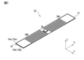
- FIG. 1 is a perspective view of a wireless communication device according to an embodiment of the present disclosure
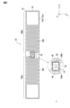
- FIG. 2 is a top view of the wireless communication device.
- the XYZ coordinate system in the figures is for facilitating understanding of the present disclosure and is not intended to limit the present disclosure.
- the X-axis direction indicates the longitudinal direction of the wireless communication device
- the Y-axis direction indicates the width direction
- the Z-axis direction indicates the thickness direction.
- the wireless communication device 10 has a strip shape and is used as a so-called RFID (Radio-Frequency IDentification) tag.
- RFID Radio-Frequency IDentification
- the wireless communication device 10 includes an antenna member 12 and an RFIC (Radio-Frequency Integrated Circuit) module 14 provided in the antenna member 12.
- RFIC Radio-Frequency Integrated Circuit
- the antenna member 12 of the wireless communication device 10 has a strip shape (elongated rectangular shape), and is provided on the antenna base material 16 and one surface 16a of the antenna base material 16 (first main surface 12a of the antenna member 12).
- antenna patterns 18A and 18B are provided on the antenna base material 16 and one surface 16a of the antenna base material 16 (first main surface 12a of the antenna member 12).
- the antenna base material 16 is a flexible sheet-like member made of an insulating material such as PET (polyethylene terephthalate). As shown in FIGS. 1 and 2, antenna substrate 16 also includes surfaces 16a, 16b that function as first major surface 12a and second major surface 12b of antenna member 12. As shown in FIGS. Since the antenna base material 16, which is a main component of the antenna member 12, is flexible, the antenna member 12 can also be flexible.
- the antenna patterns 18A and 18B are used as antennas for the wireless communication device 10 to wirelessly communicate with an external communication device (for example, a reader/writer device when the wireless communication device 10 is used as an RFID tag). Ru.
- the antenna patterns 18A and 18B are conductor patterns made of metal foil such as silver, copper, or aluminum, for example.
- the antenna patterns 18A and 18B include radiating parts 18Aa and 18Ba for transmitting and receiving radio waves, and coupling parts 18Ab and 18Bb for electrically connecting to the RFIC module 14.
- the radiating portions 18Aa and 18Ba of the antenna patterns 18A and 18B are dipole antennas and have a meander shape. Further, the radiating portions 18Aa and 18Ba each extend from coupling portions 18Ab and 18Bb provided at the central portion of the antenna base material 16 in the longitudinal direction (X-axis direction) toward both ends of the antenna base material 16.
- the coupling portions 18Ab and 18Bb of the antenna patterns 18A and 18B are electrically connected to the coupling electrode of the RFIC module 14, as will be described in detail later.
- Each of the connecting portions 18Ab and 18Bb is a rectangular land.
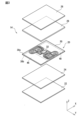
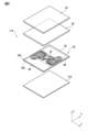
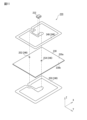
- FIG. 3 is an exploded perspective view of the RFIC module.
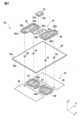
- FIG. 4 is an exploded perspective view of electronic components in the RFIC module.
- FIG. 5 is an equivalent circuit diagram of the wireless communication device.
- the RFIC module 14 is a device that performs wireless communication via antenna patterns 18A and 18B at a communication frequency in the 900 MHz band, that is, the UHF band, for example.
- the RFIC module 14 is an electronic component module with a multilayer structure including an electronic component 20.
- the RFIC module 14 includes an electronic component 20 and a hot melt adhesive layer 22 for attaching the electronic component 20 to the antenna member 12.
- the RFIC module 14 includes a bottom sheet 24 (second base material) interposed between the electronic component 20 and the hot melt adhesive layer 22, a top sheet 26, and the electronic component 20. It also includes a protective layer 28 for protecting the .
- the electronic component 20 in the RFIC module 14 includes a base sheet 30 (first base material), an RFIC chip 32 mounted on one surface 30a of the base sheet 30, and an RFIC chip 32 mounted on one surface 30a of the base sheet 30. , and a conductive pattern 36 formed on the other surface 30b (first surface) of the base sheet 30 on the opposite side to the one surface 30a.
- the base sheet 30 in the electronic component 20 of the RFIC module 14 is a thin insulating sheet made of an insulating material such as polyimide or liquid crystal polymer.
- the RFIC chip 32 is an IC chip that is driven at a frequency in the UHF band (communication frequency), and has a structure in which various elements are built into a semiconductor substrate made of a semiconductor such as silicon. Further, the RFIC chip 32 includes a first input/output terminal 32a and a second input/output terminal 32b. Furthermore, as shown in FIG. 5, the RFIC chip 32 includes an internal capacitance (capacitance: self-capacitance that the RFIC chip itself has) C1.
- the conductor pattern 34 is a pattern made of a conductor material such as silver, copper, or aluminum.
- the conductor pattern 34 includes two spiral coil portions 38 and 40.
- a land portion 38a is provided at the outer peripheral end of the coil portion 38 in the conductor pattern 34, and is electrically connected to the first input/output terminal 32a of the RFIC chip 32 via, for example, solder (not shown). ing. Further, a land portion 38b for electrically connecting to the conductive pattern 36 is provided at the center side end of the coil portion 38. Further, the tip of a branch portion 38c branched from the portion of the coil portion 38 between the outer circumference side end (land portion 38a) and the center side end (land portion 38b) is also electrically connected to the conductor pattern 36. A land portion 38d is provided for this purpose.
- the coil section 38 functions as an inductance element having an inductance L1.
- a land portion 40a is provided at the outer peripheral end of the coil portion 40 in the conductor pattern 34, and is electrically connected to the second input/output terminal 32b of the RFIC chip 32 via, for example, solder (not shown). ing. Further, a land portion 40b for electrically connecting to the conductor pattern 36 is provided at the center side end of the coil portion 40. Further, the tip of a branch portion 40c branched from the portion of the coil portion 40 between the outer circumference side end (land portion 40a) and the center side end (land portion 40b) is also electrically connected to the conductor pattern 36. A land portion 40d is provided for this purpose.
- the coil section 40 functions as an inductance element having an inductance L2.
- the conductor pattern 36 is a pattern made of a conductor material such as silver, copper, or aluminum.
- the conductor pattern 36 includes two spiral coil portions 42 and 44 and two coupling electrodes 46 and 48.
- a land portion 42a is provided at the center side end of the coil portion 42 in the conductor pattern 36.
- the land portion 42 a is electrically connected to the land portion 38 b of the coil portion 38 in the conductor pattern 34 via an interlayer connection conductor 50 such as a through-hole conductor that penetrates the base sheet 30 .
- the coil section 42 functions as an inductance element having an inductance L3, as shown in FIG.
- a land portion 44a is provided at the center side end of the coil portion 44 in the conductor pattern 36.
- the land portion 44 a is connected to the land portion 40 b of the coil portion 40 in the conductor pattern 34 via an interlayer connection conductor 52 such as a through-hole conductor that penetrates the base sheet 30 .
- the coil section 44 functions as an inductance element having an inductance L4.
- the outer circumferential ends of the two coil parts 42 and 44 are electrically connected via a connecting part 54.
- the connecting portion 54 functions as an inductance element having an inductance L5.
- Coupling electrodes 46 and 48 in the conductor pattern 36 are electrodes that are electrically connected to the RFIC chip 32 and capacitively coupled to the coupling portions 18Ab and 18Bb of the antenna patterns 18A and 18B of the antenna member 12.
- the coupling electrodes 46 and 48 have a rectangular shape and are spaced apart.
- Coil portions 42, 44 and connection portion 54 are arranged between the coupling electrodes 46, 48.
- the coupling electrode 46 is electrically connected to the land portion 38d of the coil portion 38 in the conductor pattern 34 via an interlayer connection conductor 56 such as a through-hole conductor that penetrates the base sheet 30.
- the coupling electrode 48 is electrically connected to the land portion 40d of the coil portion 40 via an interlayer connection conductor 58.
- a matching circuit 60 is configured by the coil parts 38 and 40 in the conductor pattern 34, the coil parts 42 and 44 in the conductor pattern 36, the connection part 54, and the self-capacitance C1 of the RFIC chip 32.
- This matching circuit 60 matches the impedance between the RFIC chip 32 and the coupling electrodes 46 and 48 at a predetermined frequency (communication frequency).
- a hot melt adhesive layer 22 is provided on the other surface 30b of the base sheet 30 (ie, the surface on the antenna member 12 side) of the electronic component 20 of the RFIC module 14.
- the hot melt adhesive layer 22 has a bottom sheet 24 (second base material) between the other surface 30b of the base sheet 30 and the hot melt adhesive layer 22. It is provided on the other surface 30b of the base sheet 30 in an interposed state. Further, the hot melt adhesive layer 22 is provided on the base sheet 30 so as to cover the coupling electrodes 46 and 48.
- the hot melt adhesive constituting the hot melt adhesive layer 22 softens (partially melts) when heated from a hardened state, and hardens again when cooled in the softened state.
- the hot melt adhesive is, for example, an EVA-based thermoplastic resin that maintains a hardened state and does not deform at the temperature of the environment in which the wireless communication device 10 is used.
- the hot melt adhesive layer 22 in a hardened state has insulation properties.
- the hot melt adhesive layer 22 has a low melting temperature, for example 70 to 200 degrees, compared to other components of the RFIC module 14, such as the base sheet 30. When bonding, the hot melt adhesive layer 22 is heated to, for example, about 95 degrees to soften it.
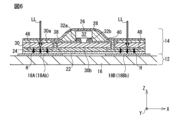
- FIG. 6 is a cross-sectional view of a portion of the wireless communication device including the RFIC module just before attachment.
- the hot melt adhesive layer 22 is interposed between the RFIC module 14 and the antenna member 12 and adheres them to each other.
- the RFIC module 14 is mounted to the antenna member 12 with the coupling electrode 46 and the coupling portion 18Ab of the antenna pattern 18A facing each other, and the coupling electrode 48 and the coupling portion 18Bb of the antenna pattern 18B facing each other. Glued. Therefore, the coupling electrode 46 and the coupling portion 18Ab are capacitively coupled with the hot melt adhesive layer 22 and the bottom sheet 24 interposed therebetween (forming a capacitance C2 as shown in FIG. 5). Further, the coupling electrode 48 and the coupling portion 18Bb are capacitively coupled with each other with the hot melt adhesive layer 22 and the bottom sheet 24 interposed therebetween (forming a capacitance C3).
- the bottom sheet 24 (second base material) interposed between the base sheet 30 and the hot melt adhesive layer 22 is made of, for example, a thermosetting resin such as an epoxy resin. Further, the bottom sheet 24 is provided on the other surface 30b of the base sheet 30 so as to cover the coupling electrodes 46 and 48. A hot melt adhesive layer 22 is provided on the surface of the bottom sheet 24 opposite to the surface facing the base sheet 30. The bottom sheet 24 is, for example, thermocompression bonded to the base sheet 30.
- the bottom sheet 24 protects the conductive pattern 36 including the coupling electrodes 46 and 48 on the other surface 30b of the base sheet 30. At the same time, the bottom sheet 24 is made up of variations in the distance between the coupling electrode 46 and the coupling part 18Ab of the antenna pattern 18A and the distance between the coupling electrode 48 and the coupling part 18Bb of the antenna pattern 18B, that is, variations in the capacitance between them. suppress.
- the hot melt adhesive layer 22 is present between the bonding electrode 46 and the bonding portion 18Ab, it is difficult to manage the distance between them. That is, when bonding the RFIC module 14 to the antenna member 12, it is necessary to control the thickness of the hot melt adhesive layer 22 so that the bonding electrode 46 and the bonding portion 18Ab are not short-circuited.
- the thickness of the bottom sheet 24 is constant, so that the coupling electrode 46 and the coupling portion 18Ab are not short-circuited. Thereby, it is possible to suppress variations in the distance between the coupling electrode 46 and the coupling portion 18Ab that would cause a short circuit.
- the top sheet 26 is an insulating sheet made of a tack-free material, for example, an insulating resin material such as PET (polyethylene terephthalate), for reasons described later. It is provided. Specifically, one surface 30a of the base sheet 30 is provided with a protective layer 28 in which at least the RFIC chip 32 is embedded.
- the protective layer 28 is made of, for example, a thermosetting resin such as an epoxy resin so that the RFIC module 14 has flexibility.
- a top sheet 26 is provided on the protective layer 28 so as to cover the protective layer 28. Thereby, the top sheet 26 and the protective layer 28 protect the IC chip 32 and the conductor pattern 34 provided on one surface 30a of the base sheet 30. Note that another sheet may exist on the top sheet 26.
- the protective layer 28 is not limited to a thermosetting resin material.
- adhesives such as hot melt agents may also be used. This improves the adhesive strength between the top sheet 26 and the base sheet 30, and also improves the flexibility of the RFIC module when the hot melt agent is softer than the thermosetting resin.
- the antenna patterns 18A, 18B when the antenna patterns 18A, 18B receive a radio wave (signal) of a predetermined frequency (communication frequency) in the UHF band, the antenna pattern 18A, 18B transmits a signal to the RFIC chip 32 corresponding to the signal. Current flows. The RFIC chip 32 is driven by the supply of the current, and outputs a current (signal) corresponding to information stored in an internal storage section (not shown) to the antenna patterns 18A and 18B. Then, radio waves (signals) corresponding to the current are radiated from the antenna patterns 18A and 18B.
- the RFIC module 14 when bonding the RFIC module 14 to the antenna member 12, the RFIC module 14 is first placed on the antenna member 12.
- the RFIC module 14 is mounted on the antenna member 12 by a mounting device (not shown).
- the hot melt adhesive layer 22 is in a cured state and has no adhesive ability.
- the parts feeder transports the plurality of RFIC modules 14 one by one to the position where the mounting apparatus picks up the RFIC modules 14 (pickup position).
- the plurality of RFIC modules 14 are in contact with each other within the parts feeder until they are transported to the pickup position.
- the top sheet 26 prevents the plurality of RFIC modules 14 from sticking to each other.
- the protective layer 28 made of thermosetting resin such as epoxy resin is exposed to the outside.
- the protective layer 28 made of thermosetting resin such as epoxy resin has tackiness. Due to its tackiness, the plurality of RFIC modules 14 stick to each other through the protective layer 28, and the handling properties of the RFIC modules 14 deteriorate.
- a tack-free top sheet 26 is provided on the protective layer 28 so as to cover the protective layer 28 so that the protective layer 28 is not exposed to the outside. That is, the top sheet 26 is made of a material with lower tackiness than that of the material of the protective layer 28, and the top sheet 26 is provided on the protective layer 28.
- Tackiness refers to so-called stickiness, and is measured using, for example, a probe tack tester.
- a probe tack tester is a device that measures the force when a defined cylindrical probe is brought into contact with the adhesive surface of the object to be measured for a short period of time and then peeled off. The greater the load when peeling off the probe, the higher the ⁇ tackiness'' of the object to be measured.
- PET is used as the material for the top sheet 26, which has a tackiness lower than that of a thermosetting resin such as an epoxy resin, which is the material of the protective layer 28.
- the top sheet 26 may be made of PI (polyimide) instead of PET.
- top sheet 26 it is possible to wind the carrier tape with the RFIC module 14 attached thereto via the outer surface of the hot melt adhesive layer 22. If the top sheet 26 is not present, the carrier tape and the protective layer 28 will stick together, making it impossible to wind the carrier tape.
- the hot melt adhesive layer 22 also has tackiness when in a cured state. In that case, hot melt adhesive layer 22 and topsheet 26 may stick to each other. To deal with this, the tackiness of the hot melt adhesive layer 22 is reduced by subjecting the outer surface of the hot melt adhesive layer 22 to a roughening treatment, such as providing fine irregularities, for example. Additionally or alternatively, the outer surface of topsheet 26 may be similarly roughened. Alternatively, a layer of a mold release agent (eg, a silicone-based mold release agent, etc.) may be provided on the outer surface of the topsheet 26. By these surface treatments, when the hot melt adhesive layer 22 has tackiness, sticking of the hot melt adhesive layer 22 and the top sheet 26 is suppressed.
- a mold release agent eg, a silicone-based mold release agent, etc.
- the hot melt adhesive layer 22 is heated and softened.
- a heating device (not shown) that emits laser light LL (white arrow) is used to heat the hot melt adhesive layer 22.
- the RFIC module 14 is configured so that the hot melt adhesive layer 22 can be heated using the laser beam LL.
- the laser beam LL has a wavelength of, for example, about 900 nm, and is applied not to the hot melt adhesive layer 22 but to the coupling electrodes 46 and 48 covered with the hot melt adhesive layer 22. irradiated.
- the coupling electrodes 46 and 48 are heated by the laser beam LL, and are brought into a high temperature state throughout.
- Heat H black arrow
- Heat H moves from the bonding electrodes 46, 48 which are in a high temperature state to the hot melt adhesive layer 22 over the entirety thereof, and as a result, the entire hot melt adhesive layer 22 is heated and softened. That is, the coupling electrodes 46, 48 function as heat spreaders.
- the portion irradiated with the laser beam LL is excessively melted before the entire hot melt adhesive layer 22 is softened. For example, there is a possibility of liquefaction.
- the bonding electrodes 46 and 48 are preferably made of a material with high light absorption.
- coupling electrodes 46, 48 are preferably made of copper.
- an oxide film (copper oxide layer) having a high light absorption rate is formed on the surface thereof. As a result, the laser beam LL is absorbed by the coupling electrodes 46 and 48 without being reflected.
- thermal resistance refers to a numerical representation of the difficulty in transmitting heat, and the larger the value, the more difficult it is to transmit heat.
- the bottom sheet 24 is interposed between the bonding electrodes 46 and 48 and the hot melt adhesive layer 22. Therefore, the thermal resistance between the coupling electrodes 46, 48 and the bottom sheet 24 is smaller than the thermal resistance between the coupling electrodes 46, 48 and the base sheet 30.
- the hot melt adhesive layer 22 can be softened efficiently and in a short time.
- Conductive particles such as carbon particles and aluminum particles are dispersed therein.
- the base sheet 30 is made of polyimide
- the bottom sheet 24 is made of epoxy resin.
- the thermal conductivity of the former is 0.28 to 0.34 [W/m ⁇ K], and the latter is 0.3 [W/m ⁇ K]. Therefore, the thermal conductivity of the materials themselves of base sheet 30 and bottom sheet 24 are approximately the same. That is, the thermal resistance between the coupling electrodes 46, 48 and the base sheet 30 and the thermal resistance between the coupling electrodes 46, 48 and the bottom sheet 24 are substantially the same. Therefore, in the case of this embodiment, conductive particles are dispersed within the bottom sheet 24.
- the bottom sheet 24 may be made from a material with a high thermal conductivity compared to the thermal conductivity of the material of the base sheet 30. This also makes it possible to make the thermal resistance between the coupling electrodes 46, 48 and the bottom sheet 24 smaller than the thermal resistance between the coupling electrodes 46, 48 and the base sheet 30.
- top sheet 26, protective layer 28, and the base sheet 30 are made of light-transmissible materials.
- the base sheet 30 is preferably made of a material with a low light absorption compared to that of the bonding electrodes 46,48. Thereby, a higher amount of laser light LL can reach the coupling electrodes 46 and 48.
- the RFIC chip 32 is provided on one surface 30a of the base sheet 30, as shown in FIGS. 2 and 3. Further, the RFIC chip 32 is provided on one surface 30a of the base sheet 30 so as not to overlap the coupling electrodes 46 and 48 when viewed in plan (viewed in the Z-axis direction). Specifically, in the case of this embodiment, the coupling electrodes 46 and 48 are arranged at intervals in the longitudinal direction (X-axis direction). An RFIC chip 32 is located between the coupling electrodes 46, 48. This prevents the laser light LL from hitting the RFIC chip 32, and allows the laser light LL to reach the coupling electrodes 46 and 48 without being obstructed by the RFIC chip 32.
- the wireless communication device 10 produced in this way is used by being attached to an article.
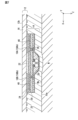
- FIG. 7 is a cross-sectional view of the wireless communication device attached to an article.
- a double-sided tape 70 is used. Specifically, the wireless communication device 10 is attached to the surface Wa of the article W via the double-sided tape 70 with the RFIC module 14 facing the surface Wa of the article W.
- the double-sided tape 70 may be a component of the wireless communication device 10. In that case, until it is attached to the article W, the wireless communication device 10 is handled with a removable mount attached to the adhesive surface 70a of the double-sided tape 70 that adheres to the article W, that is, it is handled as a sticker label. It will be done.
- the adhesive strength between the double-sided tape 70 and the top sheet 26 is determined by hot melt adhesive.
- the adhesive strength is lower than that between the agent layer 22 and the antenna member 12.
- antenna member 12 (its antenna substrate 16), bottom sheet 24, base sheet 30, protective layer 28, top sheet 26, and double-sided tape 70 are made from a substantially thermally expandable material. ing.
- the double-sided tape 70 stuck and restrained on the surface Wa of the article W becomes difficult to thermally expand.
- the top sheet 26 adhered to the double-sided tape 70 also becomes difficult to thermally expand.
- the second main surface 12b of the antenna member 12 (its antenna base material 16) is not constrained and can be freely displaced, so it tends to thermally expand.
- the hot melt adhesive layer 22 and the antenna member 12 are bonded to each other in the portion of the wireless communication device 10 between the top sheet 26, which is difficult to thermally expand, and the antenna member 12, which is easy to thermally expand. Shear forces can occur at the interface between the two. The shearing force may eventually cause the RFIC module 14 to separate from the antenna member 12.
- the adhesive strength between the double-sided tape 70 and the top sheet 26 is lower than the adhesive strength between the hot melt adhesive layer 22 and the antenna member 12.
- a layer of a release agent is provided on the outer surface of the top sheet 26 (the surface that contacts the double-sided tape 70). This reduces the adhesive strength between the double-sided tape 70 and the top sheet 26, making the top sheet 26 more susceptible to thermal expansion.
- the outer surface of the top sheet 26 may be roughened to reduce the contact area with the double-sided tape 70, thereby making it easier for the top sheet 26 to thermally expand.
- the RFIC modules 14 of the wireless communication device 10 it is possible to prevent the plurality of RFIC modules 14 from sticking to each other and reducing the handling performance.
- an insulating bottom sheet 24 is interposed between the electronic component 20 and the hot melt adhesive layer 22.
- the embodiments of the present disclosure are not limited to this.
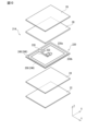
- FIG. 8 is an exploded perspective view of an RFIC module according to another embodiment of the present disclosure.
- a hot melt adhesive layer 122 is provided directly on the electronic component 20, similar to the bottom sheet 24 of the above embodiment, Coupling electrodes 46, 48 are covered. In this case, the thermal resistance between the bonding electrodes 46, 48 and the hot melt adhesive layer 122 is reduced compared to the thermal resistance between the bonding electrodes 46, 48 and the base sheet 30.
- the hot melt adhesive layer 22 for bonding the RFIC module 14 and the antenna member 12 is provided on the RFIC module 14.
- Hot melt adhesive layer 22 may be provided on antenna member 12 .
- the coupling electrodes 46 and 48 are heated by irradiation with the laser light LL. This is because the coupling electrodes 46, 48 are not exposed to the outside.
- the embodiments of the present disclosure are not limited to this. For example, a portion of the coupling electrodes 46, 48 may be exposed, a heat transfer member may be brought into contact with the exposed portion, and the heat transfer member may be heated.
- the coupling electrodes 46 and 48 of the electronic component 20 in the RFIC module 14 are capacitively coupled to the coupling portions 18Ab and 18Bb of the antenna patterns 18A and 18B of the antenna member 12. are doing.
- the coupling electrodes 46 and 48 are opposed to the coupling portions 18Ab and 18Bb with an interval in the thickness direction (Z-axis direction) of the wireless communication device 10. There is. That is, these are electrically coupled.
- embodiments of the present disclosure are not limited to electric field coupling.
- FIG. 9 is a top view of a wireless communication device according to a different embodiment of the present disclosure.
- FIG. 10 is an exploded perspective view of an RFIC module in a wireless communication device according to a different embodiment.
- FIG. 11 is an exploded perspective view of electronic components in an RFIC module of a wireless communication device according to a different embodiment.
- the antenna member 212 includes an antenna pattern 218 that magnetically couples with the RFIC module 214.
- the antenna pattern 218 connects to a substantially “C”-shaped coupling portion 218a provided so as to surround the RFIC module 214, and extends from both ends of the coupling portion 218a to each other. It includes linear radiating portions 218b and 218c extending in opposite directions.
- the RFIC module 214 includes an electronic component 220, a bottom sheet 24 interposed between the electronic component 220 and the hot melt adhesive layer 22, a top sheet 26, and a bottom sheet 24 interposed between the electronic component 220 and the hot melt adhesive layer 22; and a protective layer 28 for adhering to. Note that the bottom sheet 24 may be omitted.
- the electronic component 220 includes a base sheet 230, an RFIC chip 232 provided on the base sheet 230, and a coil conductor 246 (provided on the base sheet 230 and electrically connected to the RFIC chip 232). (coupling electrode).
- the coil conductor 246 includes a spiral conductor pattern 248 provided on one surface 230a of the base sheet 230, a spiral conductor pattern 250 provided on the other surface 230b, and a conductor pattern that penetrates the base sheet 230. 248, 250, and interlayer connection conductors 252, 254 such as through-hole conductors.
- the coil conductor 246 is provided on the base sheet 230 so as to surround the RFIC chip 232 when viewed in the thickness direction (Z-axis direction) of the wireless communication device 210.
- a current flows through the coupling portion 218a of the antenna pattern 218, thereby causing the coupling portion 218a to generate a magnetic field.
- the magnetic field causes current to flow in the coil conductor 246 of the electronic component 220 of the RFIC module 214.
- the RFIC chip 232 is driven by the supply of the current, and outputs a current to the coil conductor 246 that corresponds to information stored in an internal storage section (not shown).
- the coil conductor 246 generates a magnetic field corresponding to the output current, and the magnetic field causes a current to flow through the coupling portion 218a of the antenna pattern 218.
- the antenna pattern 218 emits radio waves corresponding to the current.
- the coil conductor 246 is heated by laser light irradiation.
- the coil conductor 246 heats and softens the hot melt adhesive layer 22, and as a result, the RFIC module 214 is bonded to the antenna member 212 via the hot melt adhesive layer 22.
- antenna patterns that can be magnetically coupled to the RFIC module 214.
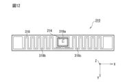
- FIGS. 12 and 13 are top views of wireless communication devices according to modified examples of different embodiments.
- the antenna pattern 318 includes a substantially “C”-shaped coupling portion 318a provided so as to surround the RFIC module 214, and both ends of the coupling 318a. It includes meander-shaped radiating portions 318b and 318c extending in opposite directions from each other.
- an antenna pattern 418 includes linear radiating portions 418a and 418b that extend parallel to each other at intervals, and one end of the linear radiating portions 418a and 418b. It includes a connecting portion 418c for connecting.
- the RFIC module 214 is surrounded by two radiating parts 418a, 418b and a connecting part 418c. Thereby, the RFIC module 214 is magnetically coupled to the antenna pattern 418.
- the electronic component module and members bonded via the hot melt adhesive layer 22 are the RFIC module 14 and the antenna member 12 in the wireless communication device, but the embodiment of the present disclosure is not limited to this. Not limited to.
- a first aspect includes a base sheet, an IC chip mounted on one surface of the base sheet, and a coupling electrode provided on the other surface of the base sheet and electrically connected to the IC chip.
- a protective layer provided on one surface of the base sheet in which the IC chip is embedded; an adhesive layer provided on the other surface of the base sheet so as to cover the bonding electrode; and an adhesive layer provided on the other surface of the base sheet so as to cover the protective layer.
- an insulating sheet provided on the protective layer, and the insulating sheet is made of a material having lower tackiness than that of the material of the protective layer. .
- a second aspect is the electronic component module of the first aspect, wherein the protective layer is made of epoxy resin and the insulating sheet is made of polyethylene terephthalate.
- a third aspect is the electronic component module according to the first or second aspect, wherein the adhesive layer is a hot melt adhesive layer, and the outer surface of the hot melt adhesive layer is roughened. It is.
- a fourth aspect is the electronic component module according to any one of the first to third aspects, wherein the outer surface of the insulating sheet is roughened.
- a fifth aspect is the electronic component module according to any one of the first to fourth aspects, further comprising a release agent layer provided on the outer surface of the insulating sheet.
- a sixth aspect includes an electronic component module, an antenna member that includes an antenna pattern that capacitively couples with the electronic component module, and to which the electronic component module is attached, and the electronic component module includes a base sheet, an IC chip mounted on one surface of the base sheet; a coupling electrode provided on the other surface of the base sheet, electrically connected to the IC chip, and electromagnetically coupled to the antenna pattern; and the base sheet. a protective layer provided on one surface of the sheet in which the IC chip is embedded; an adhesive layer provided on the other surface of the base sheet so as to cover the bonding electrode; and a protective layer provided on the other surface of the base sheet so as to cover the protective layer. an insulating sheet provided on a protective layer, the insulating sheet being made of a material having lower tackiness than that of the material of the protective layer.
- a seventh aspect further includes a double-sided tape provided on the outer surface of the insulating sheet of the electronic component module, and the adhesive strength between the double-sided tape and the insulating sheet is equal to that of the adhesive layer.
- the wireless communication device according to the sixth aspect has a lower adhesive strength than the antenna member.
- An eighth aspect is the wireless communication device according to the seventh aspect, wherein a release agent layer is provided on the outer surface of the insulating sheet.
- the present disclosure is applicable when attaching an electronic component module that includes a coupling electrode and a member that includes a conductor pattern that capacitively or magnetically couples with the coupling electrode.
Landscapes
- Engineering & Computer Science (AREA)
- Microelectronics & Electronic Packaging (AREA)
- Physics & Mathematics (AREA)
- General Physics & Mathematics (AREA)
- Theoretical Computer Science (AREA)
- Computer Hardware Design (AREA)
- Details Of Aerials (AREA)
Priority Applications (1)
| Application Number | Priority Date | Filing Date | Title |
|---|---|---|---|
| JP2024523307A JP7889604B2 (ja) | 2022-05-24 | 2023-05-23 | 電子部品モジュールおよびそれを備える無線通信デバイス |
Applications Claiming Priority (4)
| Application Number | Priority Date | Filing Date | Title |
|---|---|---|---|
| JP2022084601 | 2022-05-24 | ||
| JP2022-084601 | 2022-05-24 | ||
| JP2022118120 | 2022-07-25 | ||
| JP2022-118120 | 2022-07-25 |
Publications (1)
| Publication Number | Publication Date |
|---|---|
| WO2023228942A1 true WO2023228942A1 (ja) | 2023-11-30 |
Family
ID=88919377
Family Applications (2)
| Application Number | Title | Priority Date | Filing Date |
|---|---|---|---|
| PCT/JP2023/019152 Ceased WO2023228942A1 (ja) | 2022-05-24 | 2023-05-23 | 電子部品モジュールおよびそれを備える無線通信デバイス |
| PCT/JP2023/019147 Ceased WO2023228941A1 (ja) | 2022-05-24 | 2023-05-23 | 電子部品モジュールおよびそれを備える無線通信デバイス |
Family Applications After (1)
| Application Number | Title | Priority Date | Filing Date |
|---|---|---|---|
| PCT/JP2023/019147 Ceased WO2023228941A1 (ja) | 2022-05-24 | 2023-05-23 | 電子部品モジュールおよびそれを備える無線通信デバイス |
Country Status (4)
| Country | Link |
|---|---|
| US (1) | US20250055176A1 (cg-RX-API-DMAC7.html) |
| JP (2) | JP7889604B2 (cg-RX-API-DMAC7.html) |
| CN (1) | CN223503080U (cg-RX-API-DMAC7.html) |
| WO (2) | WO2023228942A1 (cg-RX-API-DMAC7.html) |
Citations (3)
| Publication number | Priority date | Publication date | Assignee | Title |
|---|---|---|---|---|
| JP2007256566A (ja) * | 2006-03-23 | 2007-10-04 | Osaka Sealing Printing Co Ltd | Rfidラベル及びrfidラベルの製造方法 |
| JP2013171428A (ja) * | 2012-02-21 | 2013-09-02 | Sato Holdings Corp | Rfidタグ |
| WO2020152915A1 (ja) * | 2019-01-25 | 2020-07-30 | 株式会社村田製作所 | 無線通信デバイスおよびその製造方法 |
Family Cites Families (5)
| Publication number | Priority date | Publication date | Assignee | Title |
|---|---|---|---|---|
| JP2008107947A (ja) | 2006-10-24 | 2008-05-08 | Toppan Printing Co Ltd | Rfidタグ |
| JP6046329B2 (ja) * | 2010-01-08 | 2016-12-14 | 早川ゴム株式会社 | レーザー光を用いた接合方法 |
| WO2020079962A1 (ja) | 2018-10-15 | 2020-04-23 | 株式会社村田製作所 | 無線通信デバイス |
| JP7081729B2 (ja) | 2020-04-14 | 2022-06-07 | 株式会社村田製作所 | 無線通信デバイス製造システム |
| JP7264325B1 (ja) | 2021-07-02 | 2023-04-25 | 株式会社村田製作所 | 無線通信デバイス製造システム |
-
2023
- 2023-05-23 JP JP2024523307A patent/JP7889604B2/ja active Active
- 2023-05-23 WO PCT/JP2023/019152 patent/WO2023228942A1/ja not_active Ceased
- 2023-05-23 WO PCT/JP2023/019147 patent/WO2023228941A1/ja not_active Ceased
- 2023-05-23 CN CN202390000333.7U patent/CN223503080U/zh active Active
- 2023-05-23 JP JP2024523306A patent/JP7800676B2/ja active Active
-
2024
- 2024-10-29 US US18/930,062 patent/US20250055176A1/en active Pending
Patent Citations (3)
| Publication number | Priority date | Publication date | Assignee | Title |
|---|---|---|---|---|
| JP2007256566A (ja) * | 2006-03-23 | 2007-10-04 | Osaka Sealing Printing Co Ltd | Rfidラベル及びrfidラベルの製造方法 |
| JP2013171428A (ja) * | 2012-02-21 | 2013-09-02 | Sato Holdings Corp | Rfidタグ |
| WO2020152915A1 (ja) * | 2019-01-25 | 2020-07-30 | 株式会社村田製作所 | 無線通信デバイスおよびその製造方法 |
Also Published As
| Publication number | Publication date |
|---|---|
| CN223503080U (zh) | 2025-10-31 |
| JP7800676B2 (ja) | 2026-01-16 |
| JPWO2023228941A1 (cg-RX-API-DMAC7.html) | 2023-11-30 |
| US20250055176A1 (en) | 2025-02-13 |
| WO2023228941A1 (ja) | 2023-11-30 |
| JPWO2023228942A1 (cg-RX-API-DMAC7.html) | 2023-11-30 |
| JP7889604B2 (ja) | 2026-07-14 |
Similar Documents
| Publication | Publication Date | Title |
|---|---|---|
| JP5024372B2 (ja) | 無線icデバイス | |
| US6259408B1 (en) | RFID transponders with paste antennas and flip-chip attachment | |
| US7404522B2 (en) | Information carrier, information recording medium, sensor, commodity management method | |
| EP1956873B1 (en) | RFID tag and method of manufacturing the same | |
| US7576656B2 (en) | Apparatuses and methods for high speed bonding | |
| US12014235B2 (en) | Wireless communication device | |
| MXPA97005524A (en) | Method for connecting electrically an integrated circuit to a ultraflexi substrate | |
| KR20100065186A (ko) | 인쇄 집적 회로소자를 포함하는 무선 장치 및 이의 제조 및 사용 방법 | |
| TW200913372A (en) | RFID tag | |
| US20210350199A1 (en) | Wireless communication device and method of manufacturing same | |
| JP2005275802A (ja) | 電波読み取り可能なデータキャリアの製造方法および該製造方法に用いる基板並びに電子部品モジュール | |
| US20080129455A1 (en) | Method for forming rfid tags | |
| CN101996342A (zh) | 射频识别标签及其制造方法 | |
| US7674649B2 (en) | Radio frequency identification (RFID) tag lamination process using liner | |
| US7456506B2 (en) | Radio frequency identification (RFID) tag lamination process using liner | |
| JP7800676B2 (ja) | 電子部品モジュールおよびそれを備える無線通信デバイス | |
| JP2000231614A (ja) | 電磁波読み取り可能なデータキャリア | |
| JP5786618B2 (ja) | 無線icデバイス及びその製造方法 | |
| JP2009027342A (ja) | 無線icデバイス | |
| JP2012145999A (ja) | 無線icデバイス | |
| KR101038132B1 (ko) | 무선 ic 디바이스 | |
| JP4712157B2 (ja) | 非接触式データキャリア | |
| JP5652581B1 (ja) | アンテナ装置の製造方法 | |
| JP2021128397A (ja) | Rfidタグラベル及びその使用方法 |
Legal Events
| Date | Code | Title | Description |
|---|---|---|---|
| 121 | Ep: the epo has been informed by wipo that ep was designated in this application |
Ref document number: 23811814 Country of ref document: EP Kind code of ref document: A1 |
|
| WWE | Wipo information: entry into national phase |
Ref document number: 2024523307 Country of ref document: JP |
|
| NENP | Non-entry into the national phase |
Ref country code: DE |
|
| 122 | Ep: pct application non-entry in european phase |
Ref document number: 23811814 Country of ref document: EP Kind code of ref document: A1 |