WO2023228705A1 - 通信装置 - Google Patents
通信装置 Download PDFInfo
- Publication number
- WO2023228705A1 WO2023228705A1 PCT/JP2023/017236 JP2023017236W WO2023228705A1 WO 2023228705 A1 WO2023228705 A1 WO 2023228705A1 JP 2023017236 W JP2023017236 W JP 2023017236W WO 2023228705 A1 WO2023228705 A1 WO 2023228705A1
- Authority
- WO
- WIPO (PCT)
- Prior art keywords
- antenna
- antenna element
- communication device
- inductor
- capacitor
- Prior art date
Links
- 238000004891 communication Methods 0.000 title claims abstract description 88
- 239000003990 capacitor Substances 0.000 claims abstract description 58
- 238000010248 power generation Methods 0.000 claims description 8
- 230000005404 monopole Effects 0.000 claims description 7
- 230000010287 polarization Effects 0.000 claims description 4
- 238000005516 engineering process Methods 0.000 abstract description 19
- 239000013535 sea water Substances 0.000 abstract description 14
- 238000010586 diagram Methods 0.000 description 23
- 239000002184 metal Substances 0.000 description 8
- 229910052751 metal Inorganic materials 0.000 description 8
- 239000000203 mixture Substances 0.000 description 5
- 239000007788 liquid Substances 0.000 description 4
- 239000000463 material Substances 0.000 description 4
- 230000000644 propagated effect Effects 0.000 description 4
- 230000003071 parasitic effect Effects 0.000 description 3
- BASFCYQUMIYNBI-UHFFFAOYSA-N platinum Chemical compound [Pt] BASFCYQUMIYNBI-UHFFFAOYSA-N 0.000 description 3
- 239000000758 substrate Substances 0.000 description 3
- 230000002238 attenuated effect Effects 0.000 description 2
- 230000005540 biological transmission Effects 0.000 description 2
- 239000010949 copper Substances 0.000 description 2
- 230000000694 effects Effects 0.000 description 2
- 239000011521 glass Substances 0.000 description 2
- 239000010931 gold Substances 0.000 description 2
- 238000004519 manufacturing process Methods 0.000 description 2
- 238000000034 method Methods 0.000 description 2
- 239000011347 resin Substances 0.000 description 2
- 229920005989 resin Polymers 0.000 description 2
- XLYOFNOQVPJJNP-UHFFFAOYSA-N water Substances O XLYOFNOQVPJJNP-UHFFFAOYSA-N 0.000 description 2
- 238000004804 winding Methods 0.000 description 2
- RYGMFSIKBFXOCR-UHFFFAOYSA-N Copper Chemical compound [Cu] RYGMFSIKBFXOCR-UHFFFAOYSA-N 0.000 description 1
- BQCADISMDOOEFD-UHFFFAOYSA-N Silver Chemical compound [Ag] BQCADISMDOOEFD-UHFFFAOYSA-N 0.000 description 1
- 239000000956 alloy Substances 0.000 description 1
- 229910045601 alloy Inorganic materials 0.000 description 1
- 229910052782 aluminium Inorganic materials 0.000 description 1
- XAGFODPZIPBFFR-UHFFFAOYSA-N aluminium Chemical compound [Al] XAGFODPZIPBFFR-UHFFFAOYSA-N 0.000 description 1
- 229910010293 ceramic material Inorganic materials 0.000 description 1
- 238000006243 chemical reaction Methods 0.000 description 1
- 239000004020 conductor Substances 0.000 description 1
- 229910052802 copper Inorganic materials 0.000 description 1
- 238000005260 corrosion Methods 0.000 description 1
- 230000007797 corrosion Effects 0.000 description 1
- 239000003989 dielectric material Substances 0.000 description 1
- PCHJSUWPFVWCPO-UHFFFAOYSA-N gold Chemical compound [Au] PCHJSUWPFVWCPO-UHFFFAOYSA-N 0.000 description 1
- 229910052737 gold Inorganic materials 0.000 description 1
- 230000006698 induction Effects 0.000 description 1
- CNQCVBJFEGMYDW-UHFFFAOYSA-N lawrencium atom Chemical compound [Lr] CNQCVBJFEGMYDW-UHFFFAOYSA-N 0.000 description 1
- 230000000670 limiting effect Effects 0.000 description 1
- 150000002739 metals Chemical class 0.000 description 1
- 230000003287 optical effect Effects 0.000 description 1
- 230000001151 other effect Effects 0.000 description 1
- 229910052697 platinum Inorganic materials 0.000 description 1
- 229920001296 polysiloxane Polymers 0.000 description 1
- 230000001902 propagating effect Effects 0.000 description 1
- 230000005855 radiation Effects 0.000 description 1
- 229910052710 silicon Inorganic materials 0.000 description 1
- 239000010703 silicon Substances 0.000 description 1
- 229910052709 silver Inorganic materials 0.000 description 1
- 239000004332 silver Substances 0.000 description 1
- 239000007787 solid Substances 0.000 description 1
- 230000001131 transforming effect Effects 0.000 description 1
- 238000004078 waterproofing Methods 0.000 description 1
Images


Classifications
-
- H—ELECTRICITY
- H01—ELECTRIC ELEMENTS
- H01P—WAVEGUIDES; RESONATORS, LINES, OR OTHER DEVICES OF THE WAVEGUIDE TYPE
- H01P1/00—Auxiliary devices
- H01P1/165—Auxiliary devices for rotating the plane of polarisation
- H01P1/17—Auxiliary devices for rotating the plane of polarisation for producing a continuously rotating polarisation, e.g. circular polarisation
-
- H—ELECTRICITY
- H01—ELECTRIC ELEMENTS
- H01P—WAVEGUIDES; RESONATORS, LINES, OR OTHER DEVICES OF THE WAVEGUIDE TYPE
- H01P5/00—Coupling devices of the waveguide type
- H01P5/08—Coupling devices of the waveguide type for linking dissimilar lines or devices
- H01P5/10—Coupling devices of the waveguide type for linking dissimilar lines or devices for coupling balanced with unbalanced lines or devices
-
- H—ELECTRICITY
- H01—ELECTRIC ELEMENTS
- H01Q—ANTENNAS, i.e. RADIO AERIALS
- H01Q1/00—Details of, or arrangements associated with, antennas
- H01Q1/50—Structural association of antennas with earthing switches, lead-in devices or lightning protectors
-
- H—ELECTRICITY
- H01—ELECTRIC ELEMENTS
- H01Q—ANTENNAS, i.e. RADIO AERIALS
- H01Q13/00—Waveguide horns or mouths; Slot antennas; Leaky-waveguide antennas; Equivalent structures causing radiation along the transmission path of a guided wave
- H01Q13/08—Radiating ends of two-conductor microwave transmission lines, e.g. of coaxial lines, of microstrip lines
-
- H—ELECTRICITY
- H01—ELECTRIC ELEMENTS
- H01Q—ANTENNAS, i.e. RADIO AERIALS
- H01Q21/00—Antenna arrays or systems
- H01Q21/24—Combinations of antenna units polarised in different directions for transmitting or receiving circularly and elliptically polarised waves or waves linearly polarised in any direction
-
- H—ELECTRICITY
- H01—ELECTRIC ELEMENTS
- H01Q—ANTENNAS, i.e. RADIO AERIALS
- H01Q9/00—Electrically-short antennas having dimensions not more than twice the operating wavelength and consisting of conductive active radiating elements
- H01Q9/04—Resonant antennas
- H01Q9/16—Resonant antennas with feed intermediate between the extremities of the antenna, e.g. centre-fed dipole
-
- H—ELECTRICITY
- H01—ELECTRIC ELEMENTS
- H01Q—ANTENNAS, i.e. RADIO AERIALS
- H01Q9/00—Electrically-short antennas having dimensions not more than twice the operating wavelength and consisting of conductive active radiating elements
- H01Q9/04—Resonant antennas
- H01Q9/30—Resonant antennas with feed to end of elongated active element, e.g. unipole
-
- H—ELECTRICITY
- H01—ELECTRIC ELEMENTS
- H01Q—ANTENNAS, i.e. RADIO AERIALS
- H01Q9/00—Electrically-short antennas having dimensions not more than twice the operating wavelength and consisting of conductive active radiating elements
- H01Q9/04—Resonant antennas
- H01Q9/44—Resonant antennas with a plurality of divergent straight elements, e.g. V-dipole, X-antenna; with a plurality of elements having mutually inclined substantially straight portions
Definitions
- the present technology relates to a communication device, for example, to a communication device suitable for use in communication in liquid.
- Patent Document 1 proposes a communication device that communicates with a communication device that is separated underwater.
- the present technology was developed in view of this situation, and enables stable communication even with an electrically small size antenna.
- a first communication device is a circularly polarized wave composed of a first antenna element and a second antenna element arranged orthogonally to the first antenna element.
- the phase shifter includes an antenna, a capacitor connected to the first antenna element, and an inductor connected to the second antenna element, R is a resistance, j is an imaginary unit,
- R is a resistance
- j is an imaginary unit
- the impedance of the antenna is expressed as R+jX
- a second communication device includes a circularly polarized antenna including a first antenna element and a second antenna element having orthogonal linearly polarized waves, and a circularly polarized antenna that is connected to the first antenna element.
- a phase shifter composed of a capacitor connected to the second antenna element and an inductor connected to the second antenna element, R is a resistance, j is an imaginary unit, X is a reactance, and the center frequency of the antenna is f,
- the impedance of the antenna is expressed as R+jX
- a circularly polarized wave including a first antenna element and a second antenna element arranged orthogonally to the first antenna element.
- a phase shifter is provided, which includes an antenna, a capacitor connected to the first antenna element, and an inductor connected to the second antenna element.
- R resistance
- j an imaginary unit
- X reactance
- the center frequency of the antenna is f
- capacitance is C
- inductance L
- the impedance of the antenna is expressed as R+jX
- the capacitance of the capacitor 1/ ⁇ f(R+X) ⁇
- a second communication device includes a circularly polarized antenna including a first antenna element and a second antenna element having orthogonal linearly polarized waves, and a circularly polarized antenna connected to the first antenna element. and a phase shifter including a capacitor connected to the second antenna element and an inductor connected to the second antenna element.
- the communication device may be an independent device or an internal block forming one device.
- FIG. 1 is a diagram showing the configuration of an embodiment of a communication system to which the present technology is applied.
- FIG. 3 is a diagram showing the configuration of another embodiment of a communication system to which the present technology is applied.
- FIG. 3 is a diagram showing the configuration of another embodiment of a communication system to which the present technology is applied.
- FIG. 3 is a diagram illustrating a configuration example of a master station.
- FIG. 3 is a diagram showing a configuration example of an antenna and a phase shifter.
- FIG. 3 is a diagram for explaining conditions regarding the configuration of a phase shifter. It is a figure showing the example of composition of a phase shifter. It is a figure showing the example of composition of a phase shifter.
- FIG. 3 is a diagram illustrating a configuration example of a phase shifter to which a balun is added.
- FIG. 3 is a diagram illustrating a configuration example of a phase shifter to which a balun is added.
- FIG. 2 is a diagram illustrating a configuration example of a phase shifter to which a matching circuit is added. It is a figure which shows the other example of a structure of a phase shifter. It is a figure which shows the other example of a structure of a phase shifter. It is a figure which shows the other example of a structure of a phase shifter. It is a figure which shows the other example of a structure of a phase shifter. It is a figure which shows the other example of a structure of a phase shifter.
- FIG. 3 is a diagram for explaining the shape of an antenna.
- FIG. 3 is a diagram for explaining the shape of an antenna.
- FIG. 3 is a diagram for explaining the shape of an antenna. It is a figure showing an example of composition of an antenna. It is a figure showing an example of composition of an antenna. It is a figure showing an example of composition of an antenna. It is a figure showing an example of composition of an antenna.
- FIG. 1 is a diagram showing the configuration of an embodiment of a communication system 1 to which the present technology is applied.
- the communication system 1 shown in FIG. include.
- the slave stations 21-1 to 21-6 will be simply referred to as slave stations 21 when there is no need to distinguish them individually. The same applies to other parts.
- the master station 11 and the communication station 12 perform communication using local 5G, for example.
- the master station 11 and the communication station 13 communicate using, for example, LPWA (Low Power Wide Area).
- the master station 11 is configured to be able to acquire position information from the satellite 14 using, for example, GNSS (Global Navigation Satellite System).
- GNSS Global Navigation Satellite System
- the master station 11 also communicates with the slave station 21.
- the portion of the master station 11 that communicates with the communication station 12, the communication station 13, and the satellite 14 described above is located in the air, and the portion that communicates with the slave station 21 is located in the seawater.
- the slave station 21 is located in seawater.
- the communication system 1 will be described here taking as an example the environment in which it is installed in the ocean, it can also be installed in environments such as lakes, ponds, rivers, and aquariums.
- the present technology described below can be applied to a device installed in a medium (lossy medium) other than lossless air.
- Lossy media include not only seawater and brackish lakes described above, but also the inside of the human body.
- one of the master stations 11 is located in the air (gas) and the other is located in seawater (liquid), but one may be located in the seabed (solid) or in vacuum.
- the master station 11 may also be located at a remote location.
- the configuration of the communication system 1 shown in FIG. 1 is an example and is not a limitation.
- the master station 11 communicates with the communication station 12, the communication station 13, and the satellite 14, but it may also have the function of communicating with other than these. However, instead of having the function of communicating with all of them, it may be configured to be able to communicate with one or two of them.
- the master station 11 may have a configuration in which it only has the function of communicating with the slave station 21, in other words, it does not have the function of communicating with the communication station 12, the communication station 13, or the satellite 14.
- the slave stations 21-1 to 21-6 each communicate with the master station 11.
- a so-called ad hoc network may be configured in which slave stations 21 communicate with each other.
- the slave station 21 includes, for example, a sensor that senses the underwater environment, and transmits the sensed data to the master station 11.
- the slave station 21 may be configured to have only a transmitting function for transmitting data to the master station 11, or may have a transmitting function and a receiving function for transmitting and receiving data to and from the master station 11 and other slave stations 21. It can also be configured.
- the slave station 21 is installed at a depth from the sea surface within a range of, for example, 0 to 10 m.
- the slave stations 31-1 and 31-2 each communicate with the repeater 32.
- the slave station 31 includes, for example, a sensor that senses the underwater environment, and transmits the sensed data to the repeater 32.
- the slave station 31 may be configured to have only a transmitting function for transmitting data to the repeater 32, or may have a transmitting function and a receiving function for transmitting and receiving data to and from the repeater 32 and other slave stations 31. It can also be configured.
- the slave station 31 is installed on the ocean floor (near the ocean floor).
- the antenna that is installed in seawater (liquid) and used for communication with the slave station 21 and repeater 32 installed in the seawater is a circularly polarized antenna.
- the antennas of the slave station 21 and the slave station 31 may be circularly polarized antennas or linearly polarized antennas.
- the antenna of the repeater 32 is a circularly polarized antenna, and in the example shown in FIG. 1, it is used when communicating with the slave station 31 and when communicating with the master station 11.
- the relay 32 and the master station 11 may be configured to communicate by wire.
- optical communication may be used between the repeater 32 and the master station 11.
- the slave station 21 and the slave station 31 are grounded in the sea or on the seabed, the positional relationship with the master station 11 and the repeater 32 may deviate from the positional relationship suitable for communication due to the influence of waves.
- a circularly polarized antenna as the antenna on the receiving side that receives data from the master station 11 and the repeater 32, in other words, the slave station 21 and the slave station 31, it is possible to prevent Even in this case, relatively good communication can be maintained.
- the signal from the slave station 21 installed underwater is propagated to the master station 11 through a direct wave that travels in a straight line between the antenna of the slave station 21 and the antenna of the master station 11, and a direct wave that propagates in a straight line between the antenna of the slave station 21 and the antenna of the master station 11.
- the lateral wave becomes dominant and is received by the master station 11. Since lateral waves propagate farther than direct waves, the greater the distance between slave station 21 and master station 11, the more lateral waves become dominant. This phenomenon occurs when the antenna is not far from the sea surface.
- the signal from the slave station 31 installed on the ocean floor is propagated to the repeater 32 through a direct wave that travels in a straight line between the antenna of the slave station 31 and the antenna of the repeater 32, and a direct wave that propagates in a straight line between the antenna of the slave station 31 and the antenna of the repeater 32.
- the signal propagated from the slave station 31 into the seawater has a large attenuation, but the signal propagated along the seabed from the slave station 31 has a small attenuation. is received. Signals propagating along the ocean floor allow networks to be spread over larger areas. Power consumption of the slave station 31 can be reduced. When a mesh network is configured by the slave stations 31, the number of terminals required for the mesh network can be reduced.
- FIG. 4 is a diagram showing an example of the configuration of the master station 11.
- the master station 11 shown in FIG. 4 includes a signal processing section 101, a high frequency processing section 102, and an antenna 103.
- Antenna 103 of master station 11 is installed in seawater (liquid) and is used for communication with slave station 21, repeater 32, and other master stations 11 installed in seawater.
- Antenna 103 is a circularly polarized antenna.
- the signal from the slave station 21 is received by the antenna 103 of the master station 11 and supplied to the high frequency processing section 102.
- the high frequency processing unit 102 is configured to process, for example, a received signal and a transmitted signal.
- the operating frequency fw of the high frequency processing section 102 is set to, for example, 1 MHz or less.
- the signal processed by the high frequency processing section 102 is supplied to the signal processing section 101.
- the signal processing unit 101 performs processing such as temporarily storing a signal processed by the high frequency processing unit 102 or processing a received signal and transmitting the processed signal.
- the configuration of the master station 11 shown in FIG. 4 can also be applied to the configuration of the repeater 32.
- the antenna 103 has the function of receiving signals from the slave station 31 and the function of transmitting signals to the master station 11 or other repeaters 32.
- the high frequency processing section 102 and the signal processing section 101 have a function of amplifying a received signal and transmitting it.
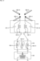
- FIG. 5 is a diagram showing a configuration example of the antenna 103 and the phase shifter 111 included in the high frequency processing section 102.
- the antenna 103 and phase shifter 111 included in the master station 11 will be explained as an example, but it is also applicable to any of the slave stations 21, 31, and repeaters 32. .
- the antenna 103 is a circularly polarized antenna, and in the example shown in FIG. 5, it is composed of antenna elements 103-1 to 103-4.
- a pair of antenna elements 103-1 and 103-2 are arranged on a straight line and constitute a dipole antenna.
- the pair of antenna elements 103-3 and 103-4 are arranged on a straight line and constitute a dipole antenna.
- a dipole antenna consisting of antenna element 103-1 and antenna element 103-2 and a dipole antenna consisting of antenna element 103-3 and antenna element 103-4 are arranged so as to intersect at 90 degrees.
- the antenna 103 is a cross dipole antenna composed of antenna elements 103-1 to 103-4, and is a circularly polarized antenna.
- the antenna 103 shown in FIG. 5 uses two sets of balanced linearly polarized antennas, and the antenna elements (radiating elements) constituting the orthogonally polarized antennas are arranged so as to be orthogonal to each other, resulting in circular polarization.
- An antenna that can transmit and receive wave signals.
- Antenna element 103-1 and antenna element 103-2 are connected to phase shifter 111-2.
- Antenna element 103-3 and antenna element 103-4 are connected to phase shifter 111-1.
- the master station 11 including the phase shifter 111 having such a configuration is installed in a medium having high conductivity such as seawater.
- a medium having high conductivity electromagnetic waves are attenuated significantly, and when communication is performed over a distance of several meters, communication is generally performed using a frequency below the MHz band.
- the length of one wavelength is on the order of several meters, and for example, the size of a half-wavelength antenna may be considerably large compared to the communication device.
- the length of one wavelength is on the order of several meters, and if the antenna 103 is a resonant antenna such as a half-wavelength dipole antenna, the size of the antenna 103 may become large.
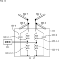
- FIG. 6 is a diagram in which the impedance in the phase shifter 111 is added to the phase shifter 111 and the antenna 103 shown in FIG. 5.
- the impedance of the electrically small antenna (antenna 103) shown in FIG. 6 is R+jX.
- R in impedance R+jX is the real part of impedance and represents resistance.
- jX of R+jX is the imaginary part of impedance, j represents an imaginary unit, and X represents reactance.
- Impedance R+jX is the impedance of one pair of antenna elements 103, for example, antenna element 103-1 and antenna element 103-2, when viewed from the phase shifter 111 side.
- the impedance of phase shifter 111-1 when viewed from the power feeding side is Ra+jXa
- the impedance when antenna 103 is viewed from phase shifter 111-1 is R+jX.
- the impedance to phase shifter 111-2 is Rb+jXb
- the impedance from phase shifter 111-1 is R+jX.
- each orthogonal antenna In order to obtain circularly polarized waves by orthogonally arranging a dipole antenna consisting of antenna elements 103-1 and 103-2 and a dipole antenna consisting of antenna elements 103-3 and 103-4, the impedance of each orthogonal antenna must be adjusted.
- the phase shifter 111 may be connected to each antenna 103 so that the phase difference between the two antennas is 90 degrees.
- the condition for the phase difference to be 90 degrees is expressed by the following equation (1).
- Ra ⁇ Rb+Xa ⁇ Xb 0 (1)
- the phase shifter 111-1 has a capacitance C shown by the following equation (5)
- the phase shifter 111-2 has a capacitance C shown by the following equation (6).
- a configuration having an inductance L may be used.
- f represents the center frequency of the frequency to be transmitted or received (desired frequency).
- the phase shifter 111-1 includes a capacitor 121-1 and a capacitor 121-2 having a capacitance C calculated by equation (5).
- the phase shifter 111-2 includes an inductor 122-1 and an inductor 122-2 having an inductance L calculated by equation (6).
- Capacitor 121-1 in phase shifter 111-1 is provided between a high frequency power source (not shown) and antenna element 103-4, and capacitor 121-2 is provided between high frequency power source and antenna element 103-3. It is set in.
- Inductor 122-1 in phase shifter 111-2 is provided between the high frequency power source and antenna element 103-2, and inductor 122-2 is provided between the high frequency power source and antenna element 103-1. There is.
- phase shifter 111-1 and phase shifter 111-2 in FIG. 7 are collectively referred to as phase shifter 111.
- the phase shifter 111 includes an inductor 122-1 and an inductor 122-2 connected to the antenna element 103-1 and the antenna element 103-2, respectively. Further, phase shifter 111 includes a capacitor 121-1 and a capacitor 121-2 connected to antenna element 103-3 and antenna element 103-4, respectively.
- Capacitor 121-1 of phase shifter 111 is provided between a high frequency power source (not shown) and antenna element 103-4, and inductor 122-2 is provided between the high frequency power source and antenna element 103-1. ing. On the power supply side, capacitor 121-1 and inductor 122-2 are short-circuited.
- Capacitor 121-2 of phase shifter 111 is provided between the high frequency power source and antenna element 103-3, and inductor 122-1 is provided between the high frequency power source and antenna element 103-2. On the power supply side, capacitor 121-2 and inductor 122-1 are short-circuited.
- phase shifter 111 By configuring the phase shifter 111 in this way, it is possible to configure an ideal circularly polarized antenna with an axial ratio of 1 at the frequency f. Further, the phase shifter 111 that can obtain such an effect can be realized using four lumped constants. Therefore, the master station 11, the slave stations 21 and 31, and the repeater 32 including the phase shifter 111 and the antenna 103 can be downsized and manufactured at low cost.
- FIG. 9 is a diagram showing another configuration example of the phase shifter 111.
- the phase shifter 111 shown in FIG. 9 differs from the phase shifter 111 shown in FIG. 8 in that a balun 141 is added, and is similar in other respects. Inserting a balun can reduce noise and stabilize characteristics.
- the balun 141 illustrated in FIG. 9 is a float balun and includes a transformer 142-1 and a transformer 142-2. These two transformers are constructed by, for example, bifilar winding around the glasses core so that the polarities are the same.
- FIG. 10 is an example of the configuration of the phase shifter 111 to which a balun is added.
- the added balun 151 is a balun called a forced balun.
- the balun 151 is composed of transformers 151-1 to 151-3.
- the balun 151 is, for example, a toroidal core with three wires wound in a trifilar manner and wired so as to have an impedance conversion ratio of 1:1, and forcibly converts between balanced and unbalanced states.
- a matching circuit 161 may be added to the balun 151.
- the matching circuit 161 includes a transformer composed of a primary coil and a secondary coil, and transmits power by using mutual induction between the primary coil and the secondary coil. , impedance matching is performed by converting the voltage and impedance depending on the winding ratio of the two coils.
- FIG. 11 shows a configuration in which a matching circuit 161 is added to the balun 151
- a configuration in which the matching circuit 161 is added to the balun 141 may also be used.
- FIG. 12 is a diagram showing the configuration of another phase shifter 111.
- the phase shifter 111 shown in FIG. 12 has the same configuration as the phase shifter 111 shown in FIG. They are different in that they are composed of , and are similar in other respects.
- the capacitors 121-1' and 121-1' can be capacitors whose capacitance is variable by external control, such as a varicap.
- the phase shifter 111 is included in the master station 11, for example, and the master station 11 is assumed to be affected by the surrounding environment.
- the impedance of the antenna 103 may change due to the influence of the surrounding environment on the master station 11.
- the capacitance of the capacitor 121 is made variable so that it can follow such changes in the impedance of the antenna 103 and return (adjust) it to an appropriate impedance.
- the inductor 122 may also be variable. Further, both the capacitor 121 and the inductor 122 may be variable. At least one of the capacitor 121 and the inductor 122 can be configured to be variable.
- the phase shifter 111 may be provided with an adjustment section that adjusts the variable capacitor 121 and/or inductor 122 in accordance with changes in impedance.
- a configuration may also be adopted in which the balun 141 (FIG. 9) or the balun 151 (FIG. 10) is connected to the phase shifter 111 shown in FIG. 12. Furthermore, a configuration may be adopted in which a balun 151 (141) and a matching circuit 161 are connected to the phase shifter 111 shown in FIG.
- FIG. 13 is a diagram showing the configuration of another phase shifter 111.
- the phase shifter 111 shown in FIG. 13 is similar to the phase shifter 111 shown in FIG. 8 except that a resistor 201 is added.
- ESR equivalent series resistance
- a compensation circuit may be included so that the ideal capacitance C and inductance L calculated using equations (5) and (6) are achieved.
- a resistor 201 having a resistance value corresponding to the equivalent series resistance is provided on the capacitor 121 side so that the equivalent series resistance of the inductor 122 does not upset the impedance balance.
- a resistor 201-1 is connected in series to the capacitor 121-1 of the phase shifter 111, and a resistor 201-2 is connected in series to the capacitor 121-2.
- the phase shifter 111 shown in FIG. 14 shows a configuration example in which an inductor 122 is provided in parallel as a compensation circuit.
- an inductor 122-1-1 and an inductor 122-1-2 are connected in parallel, one end is connected to the antenna element 103-2, and the other end is connected to a power source (not shown). It is connected.
- an inductor 122-2-1 and an inductor 122-2-2 are connected in parallel, one end is connected to the antenna element 103-1, and the other end is connected to a power source (not shown). It is connected to the.
- the inductors 122 By arranging the inductors 122 in parallel, a configuration can be achieved in which the influence of the equivalent series resistance of the inductors 122 can be reduced. Furthermore, if the inductance L shown in equation (6) cannot be obtained with one inductor 122, for example, there is no element in the E12 series or E24 series that corresponds to the inductance L calculated by equation (6). In this case, by using a plurality of inductors 122, it is possible to configure the inductance L to be calculated by equation (6).
- the inductors 122 may be connected in series, as shown in FIG. 15, instead of being connected in parallel.
- the phase shifter 111 shown in FIG. 15 shows a configuration example in which an inductor 122 is provided in series as a compensation circuit, and an adjustment section 221 is added.
- an inductor 122-1-1 and an inductor 122-1-2 are connected in series, one end is connected to the antenna element 103-2, and the other end is connected to a power source (not shown). It is connected.
- an inductor 122-2-1 and an inductor 122-2-2 are connected in series, one end is connected to the antenna element 103-1, and the other end is connected to a power source (not shown). It is connected to the.
- An adjustment section 221 is provided between the inductors 122-1-1 and 122-1-2 and between the inductors 122-2-1 and 122-2-2, which are connected in series. This adjustment section 221 adjusts the inductance L of the inductor 122-1 composed of the inductor 122-1-1 and the inductor 122-1-2, and the inductance L of the inductor 122-1 composed of the inductor 122-2-1 and the inductor 122-2-2. The inductance L of 122-2 is adjusted.
- a configuration may also be adopted in which the balun 141 (FIG. 9) or the balun 151 (FIG. 10) is connected to the phase shifter 111 shown in FIGS. 12 to 15. Furthermore, a configuration may be adopted in which a balun 151 (141) and a matching circuit 161 are connected to the phase shifter 111 shown in FIGS. 12 to 15.
- the structure is such that circuits such as the phase shifter 111 are protected with resin such as silicone for waterproofing.
- parasitic impedance may occur with materials such as silicon.
- the configuration may include a compensation circuit that takes into consideration the occurrence of such parasitic impedance that occurs during operation.
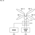
- FIG. 16 is a diagram showing an example of a configuration in which the antenna is configured with a propeller antenna 301.
- the antenna shown in FIG. 16 is composed of antenna elements 301-1 to 301-4, and is configured in a propeller type.
- the propeller-shaped antenna element 301 has a shape that rotates by wave power or tidal power.
- each antenna element 301 is processed into a shape that easily receives wave force, and the antenna 301 is processed into a shape that is easily rotated by wave force.
- the antenna element 301 constitutes a cross dipole antenna like the above-mentioned antenna element 103 (FIG. 8).
- Antenna element 301 is connected to phase shifter 111.
- the phase shifter 111 has a configuration to which any of the phase shifters 111 described with reference to FIGS. 8 to 15 is applied.
- the output from the phase shifter 111 is supplied to a movable contact section 311 using a slip ring or the like.
- a terminal connected to the antenna element 301 is provided on the antenna element 301 side of the movable contact portion 311, and the terminal is configured to rotate in accordance with the rotation of the antenna element 301.
- the terminal provided in contact with the rotating terminal is a fixed terminal and is connected to the transmitting/receiving circuit 312.
- the transmitting/receiving circuit 312 processes the signal received by the antenna element 301 that is supplied via the movable contact portion 311. Further, the transmitting/receiving circuit 312 generates a signal to be transmitted by the antenna element 301 and supplies it to the antenna element 301 via the movable contact portion 311 .
- a power generation section 313 is also connected to the movable contact section 311.
- the power generation unit 313 generates power using the rotation of the antenna 301.
- the power generated by the power generation unit 313 may be stored in a storage battery (not shown).
- the master station 11, slave stations 21 and 31, and repeater 32 that have such an antenna 301 and power generation section 313 can operate with the power generated by the power generation section 313.
- FIG. 17 is a diagram for explaining another shape of the antenna.
- the antenna shown in FIG. 17 is composed of spherical antenna elements 351-1 to 351-4.
- FIG. 18 shows the configuration of one pair of antennas 301.
- One pair constituting the antenna 301 for example, antenna element 351-1 and antenna element 351-2, includes a pair of electrodes 351 and a sheath 355.
- the sheath portion 355 includes a pair of wires 353 that electrically connect the electrode 351 and the power supply terminal corresponding to the electrode 351.
- the sheath portion 355 has, for example, a columnar shape extending in a direction connecting the pair of electrodes 351. The shape of this column is assumed to be a cylinder or a prismatic shape.
- the sheath 355 may include a low-loss dielectric therein.
- the low-loss dielectric include air, pure water, resin, glass, and ceramic materials. Note that the low-loss dielectric inside the sheath portion 355 may be made of a plurality of materials.
- the shape of the electrode 351 can be spherical, as shown in A in FIG. 18, and any shape close to a sphere is sufficient.
- the shape may be a spheroid.
- the surface may not be smooth, and may have a polyhedral shape as shown in FIG. 18C. At this time, it can be made into an icosahedron or more. The shape may be other than a regular polyhedron.
- the electrode 351 Regardless of the shape of the electrode 351, its minimum diameter is larger than the width of the wiring 353.
- a dielectric material may be provided inside the electrode 351. In this case, the dielectric inside the electrode 351 may be made of a plurality of materials.
- the transmission characteristics of the antenna for wireless communication via a lossy medium can be improved.
- a balanced antenna was used as an example.
- the present technology is not limited to application to balanced antennas, but can also be applied to unbalanced antennas. Below, a case where the present technology is applied to an unbalanced antenna will be explained.
- the antenna 401 shown in FIG. 19 is an antenna that realizes circular polarization by feeding power to orthogonal linearly polarized radiation elements 411-1 and 411-2 with a phase difference of 90 degrees.
- the radiating element 411-1 and the radiating element 411-2 shown in FIG. 19 are each a linearly polarized microstrip antenna (sometimes referred to as a patch antenna).
- a microstrip antenna is a planar antenna whose components include a dielectric substrate, a radiating element (antenna element) printed and wired on both sides of the dielectric substrate, and a ground conductor plate.
- phase shifter 421 is connected to the antenna 401.
- Phase shifter 421 includes an inductor 423 and a capacitor 425.
- Inductor 423 is connected to radiating element 411-1, and capacitor 425 is connected to radiating element 411-2.
- the sides of the inductance 423 and the capacitance 425 opposite to the antenna 401 side are short-circuited.
- the back surface (the surface opposite to the surface on which the radiating element 411 is provided) of the dielectric substrate constituting the antenna 401 is entirely grounded.
- the formula for calculating the capacitance C corresponding to the above-mentioned formula (5) is the following formula (7)
- the formula for calculating the inductance L corresponding to the above-mentioned formula (6) is the following formula ( 8).
- the capacitor 425 constituting the phase shifter 421 has a capacitance C calculated by equation (7), and the inductor 423 has an inductance L calculated by equation (8).
- FIG. 20 is a diagram for explaining still another shape of the antenna.
- Antenna 401 shown in FIG. 20 is a circularly polarized microstrip antenna. It is also possible to create a circularly polarized wave by making a notch in the radiating element of the microstrip antenna and use it as the circularly polarized antenna 401.
- the signal supplied to the radiating element 413 via the inductor 423 of the phase shifter 421 is a signal whose phase is shifted by 90 degrees from the signal supplied to the radiating element 413 via the capacitor 425.
- FIG. 21 is a diagram for explaining still another shape of the antenna.
- Antenna 401 shown in FIG. 21 is an antenna to which a monopole antenna is applied.
- the antenna 401 includes an L-shaped metal plate 431.
- the metal plate 431 has two orthogonal surfaces, with a hole 433-1 formed in one surface (metal plate 431-1) and a hole 433-1 formed in the other surface (metal plate 431-2). -2 is formed.
- a wire is passed through the hole 433-1, one of which is connected to the inductor 423 of the phase shifter 421, and the other is connected to the antenna element 435-1.
- One set of monopole antenna is constructed from the antenna element 435-1 and the metal plate 431-1.
- a wire is passed through the hole 433-2, one of which is connected to the capacitor 425 of the phase shifter 421, and the other wire is connected to the antenna element 435-2.
- One set of monopole antenna is constructed from the antenna element 435-2 and the metal plate 431-2.
- the antenna 401 has a configuration in which two sets of monopole antennas are arranged in an orthogonal positional relationship.
- the antenna 401 functions as a circularly polarized antenna by arranging two sets of monopole antennas orthogonally and supplying signals whose phases are shifted by 90 degrees.
- one or both of the inductor 423 and the capacitor 425 are configured to be variable, as described with reference to FIG. 12, so that adjustments can be made in accordance with changes in the environment. It is also possible to have a configuration that allows this.
- a configuration may also be adopted in which the balun 141 (FIG. 9) or the balun 151 (FIG. 10) is connected to the phase shifter 421 shown in FIGS. 19 to 21. Furthermore, a configuration may be adopted in which the balun 151 (141) and the matching circuit 161 are connected to the phase shifter 421 shown in FIGS. 19 to 21.
- phase shifter 421 shown in FIGS. 19 to 21 As explained with reference to FIGS. It is also possible to adopt a configuration in which the adjustment section 221 is connected to the controller 221 or a configuration in which the adjustment section 221 is provided.
- the circularly polarized antenna may have a configuration other than that exemplified here.
- system refers to the entire device configured by a plurality of devices.
- the present technology can also have the following configuration.
- R resistance
- j an imaginary unit
- X reactance
- the center frequency of the antenna is f
- capacitance is C
- inductance L
- the impedance of the antenna is expressed as R+jX
- the communication device according to (1) wherein the antenna is a balanced antenna.
- the first antenna element and the second antenna element are each dipole antennas, Both of the two radiating elements constituting the first antenna element are each connected to a capacitor,
- the communication device according to any one of (1) to (6), wherein at least one of the capacitor and the inductor is variable.
- a resistor having a resistance value corresponding to an equivalent series resistance of the inductor is connected to the capacitor.
- the inductor has a configuration in which a plurality of inductors are connected in parallel or in series.
- the antenna is a propeller antenna, The communication device according to any one of (1) to (9), further comprising a power generation unit that generates power by rotating the propeller antenna.
- a circularly polarized antenna comprising a first antenna element and a second antenna element with orthogonal linear polarization; a capacitor connected to the first antenna element; an inductor connected to the second antenna element; and a phase shifter comprising:
- R resistance
- j an imaginary unit
- X reactance
- the center frequency of the antenna is f
- capacitance is C
- inductance L
- the impedance of the antenna is expressed as R+jX
- the communication device according to (11), wherein the antenna is an unbalanced antenna.
- the communication device according to (11) or (12), wherein the first antenna element and the second antenna element are each monopole antennas.
- the communication device according to any one of (11) to (14), wherein the capacitor and the inductor are short-circuited.
- the communication device according to any one of (11) to (15), wherein at least one of the capacitor and the inductor is variable.
Abstract
本技術は、電気的に小さいサイズのアンテナでも安定した通信を行うことができるようにする通信装置に関する。 第1のアンテナ素子と、第1のアンテナ素子に対して直交するように配置された第2のアンテナ素子とから構成される円偏波のアンテナと、第1のアンテナ素子に接続されているキャパシタと、第2のアンテナ素子に接続されているインダクタとから構成される移相器とを備え、Rをレジスタンス、jを虚数単位、Xをリアクタンス、アンテナの中心周波数をf、キャパシタンスをC、インダクタンスをLとした場合、アンテナのインピーダンスは、R+jXと表され、キャパシタのキャパシタンスは、C=1/{πf(R+X)}で算出される値であり、インダクタのインダクタンスは、L=(R-X)/(4πf)で算出される値である。本技術は、例えば、海水中に設置された通信装置に適用できる。
Description
本技術は通信装置に関し、例えば、液体中の通信に用いて好適な通信装置に関する。
近年、無線LAN(Local Area Network)や非接触通信などの無線通信が広く普及している。特許文献1では、水中で離隔する通信装置と通信を行う通信装置についての提案がなされている。
水中、例えば海水中は、高い導電率により電磁波の減衰が大きいため、通信周波数としては、一般的には、MHz帯域以下の周波数が選択される。また高い誘電率の媒質中では、アンテナが共振しづらいため、そのような媒質中で用いることを前提とした共振型のアンテナの設計は困難であった。このようなことから、海水中で通信を行うためのアンテナに、例えば半波長ダイポールアンテナのような一般的な共振型のアンテナを用いた場合だと、1波長の長さが数mオーダーとなり、アンテナサイズが大きくなってしまい、その設計も困難であった。
海水中など、高い導電率の媒体においても、電気的に小さいサイズのアンテナで安定した通信を行えるようにすることが望まれている。
本技術は、このような状況に鑑みてなされたものであり、電気的に小さいサイズのアンテナでも安定した通信を行うことができるようにするものである。
本技術の一側面の第1の通信装置は、第1のアンテナ素子と、前記第1のアンテナ素子に対して直交するように配置された第2のアンテナ素子とから構成される円偏波のアンテナと、前記第1のアンテナ素子に接続されているキャパシタと、前記第2のアンテナ素子に接続されているインダクタとから構成される移相器とを備え、Rをレジスタンス、jを虚数単位、Xをリアクタンス、前記アンテナの中心周波数をf、キャパシタンスをC、インダクタンスをLとした場合、前記アンテナのインピーダンスは、R+jXと表され、前記キャパシタのキャパシタンスは、C=1/{πf(R+X)}で算出される値であり、前記インダクタのインダクタンスは、L=(R-X)/(4πf)で算出される値である通信装置である。
本技術の一側面の第2の通信装置は、直交する直線偏波の第1のアンテナ素子と第2のアンテナ素子から構成される円偏波のアンテナと、前記第1のアンテナ素子に接続されているキャパシタと、前記第2のアンテナ素子に接続されているインダクタとから構成される移相器とを備え、Rをレジスタンス、jを虚数単位、Xをリアクタンス、前記アンテナの中心周波数をf、キャパシタンスをC、インダクタンスをLとした場合、前記アンテナのインピーダンスは、R+jXと表され、前記キャパシタのキャパシタンスは、C=1/{2πf(R+X)}で算出される値であり、前記インダクタのインダクタンスは、L=(R-X)/(2πf)で算出される値である通信装置である。
本技術の一側面の第1の通信装置においては、第1のアンテナ素子と、前記第1のアンテナ素子に対して直交するように配置された第2のアンテナ素子とから構成される円偏波のアンテナと、前記第1のアンテナ素子に接続されているキャパシタと、前記第2のアンテナ素子に接続されているインダクタとから構成される移相器とが備えられる。Rをレジスタンス、jを虚数単位、Xをリアクタンス、前記アンテナの中心周波数をf、キャパシタンスをC、インダクタンスをLとした場合、前記アンテナのインピーダンスは、R+jXと表され、前記キャパシタのキャパシタンスは、C=1/{πf(R+X)}で算出される値であり、前記インダクタのインダクタンスは、L=(R-X)/(4πf)で算出される値である。
本技術の一側面の第2の通信装置においては、直交する直線偏波の第1のアンテナ素子と第2のアンテナ素子から構成される円偏波のアンテナと、前記第1のアンテナ素子に接続されているキャパシタと、前記第2のアンテナ素子に接続されているインダクタとから構成される移相器とが備えられる。Rをレジスタンス、jを虚数単位、Xをリアクタンス、前記アンテナの中心周波数をf、キャパシタンスをC、インダクタンスをLとした場合、前記アンテナのインピーダンスは、R+jXと表され、前記キャパシタのキャパシタンスは、C=1/{2πf(R+X)}で算出される値であり、前記インダクタのインダクタンスは、L=(R-X)/(2πf)で算出される値である。
なお、通信装置は、独立した装置であっても良いし、1つの装置を構成している内部ブロックであっても良い。
以下に、本技術を実施するための形態(以下、実施の形態という)について説明する。
<通信システムの構成>
図1は、本技術を適用した通信システム1の一実施の形態の構成を示す図である。図1に示した通信システム1は、親局11、通信局12、通信局13、衛星14、子局21-1乃至21-6、子局31-1,31-2、および中継器32を含む。以下の説明において、子局21-1乃至21-6を、個々に区別する必要が無い場合、単に子局21と記述する。他の部分も同様とする。
図1は、本技術を適用した通信システム1の一実施の形態の構成を示す図である。図1に示した通信システム1は、親局11、通信局12、通信局13、衛星14、子局21-1乃至21-6、子局31-1,31-2、および中継器32を含む。以下の説明において、子局21-1乃至21-6を、個々に区別する必要が無い場合、単に子局21と記述する。他の部分も同様とする。
親局11と通信局12は、例えば、ローカル5Gを用いた通信を行う。親局11と通信局13は、例えば、LPWA(Low Power Wide Area)を用いた通信を行う。親局11は、衛星14からの例えば、GNSS(Global Navigation Satellite System)を用いた位置情報の取得を行えるように構成されている。ここでは、ローカル5G、LPWA、GNSSを例に挙げて説明を続けるが、他の通信網、例えば、WLAN(Wireless Local Area Network)や衛星通信網などを用いた通信が行われるように構成することも可能である。
親局11は、子局21とも通信を行う。親局11のうち、上記した通信局12、通信局13、および衛星14と通信を行う部分は、空気中に位置し、子局21と通信を行う部分は、海水中に位置している。子局21は、海水中に位置している。
なおここでは、通信システム1が設置されている環境が海である場合を例に挙げて説明するが、湖、池、川、水槽などの環境に設置することも可能である。以下に説明する本技術は、無損失な空気中以外の媒質(損失性媒質)に設置される装置に適用できる。損失性媒質には、上記した海水中、汽水湖中などの他に、人体内部なども含まれる。
ここでは親局11の一方は、空気中(気体中)に位置し、他方は海水中(液体中)に位置するとして説明するが、一方が海底中(固体中)に位置したり、真空中に位置したりするような親局11であっても良い。
図1に示した通信システム1の構成は一例であり限定を示す記載ではない。図1に示した通信システム1において親局11は、通信局12、通信局13、および衛星14と通信を行う例を示しているが、これら以外と通信を行う機能をさらに有していても良いし、これらの全てと通信できる機能を有しているのではなく、いずれか1つまたは2つと通信できるように構成されていても良い。親局11は、子局21と通信する機能のみを有している、換言すれば、通信局12、通信局13、または衛星14と通信する機能を有していない構成とすることもできる。
子局21-1乃至21-6はそれぞれ、親局11と通信を行う。子局21同士が通信を行う、所謂、アドホックネットワークが構成されているようにしても良い。子局21は、例えば、海中内をセンシングするセンサを備え、センシングしたデータを、親局11に送信する。子局21は、親局11に対してデータを送信する送信機能だけを有する構成とすることもできるし、親局11や他の子局21とデータの送受信を行う送信機能と受信機能を有する構成とすることもできる。子局21は、海面からの深さが、例えば0乃至10mの範囲内に設置される。
子局31-1乃,31-2はそれぞれ、中継器32と通信を行う。子局31は、例えば、海中内をセンシングするセンサを備え、センシングしたデータを、中継器32に送信する。子局31は、中継器32に対してデータを送信する送信機能だけを有する構成とすることもできるし、中継器32や他の子局31とデータの送受信を行う送信機能と受信機能を有する構成とすることもできる。子局31は、海底(海底付近)に設置される。
親局11のアンテナのうち、海水中(液体中)に設置され、海水中に設置されている子局21、中継器32との通信に用いられるアンテナは、円偏波のアンテナである。子局21と子局31のアンテナは、円偏波のアンテナでも良いし、直線偏波のアンテナでも良い。中継器32のアンテナは、円偏波のアンテナであり、図1に示した例では、子局31と通信を行うときと、親局11と通信を行うときに用いられる。
図2に示すように、中継器32と親局11との間は、有線による通信が行われるように構成することもできる。図3に示すように、中継器32と親局11との間は、光通信が用いられて行われるように構成することもできる。
子局21や子局31は、海中や海底に接地されるが、波の影響などにより親局11や中継器32との位置関係が通信に適した位置関係からずれてしまう可能性がある。親局11や中継器32、換言すれば、子局21や子局31からのデータを受信する受信側のアンテナを、円偏波のアンテナとすることで、適切な位置関係からずれたような場合でも、比較的良好な通信を維持することができる。
海中に設置された子局21からの信号が、親局11に伝搬される経路としては、子局21のアンテナと親局11のアンテナとの間を、直線的に進む直接波と、子局21のアンテナからその直上の海面まで鉛直上向きに進み、海面に出て、海面に沿って進み、親局11のアンテナの直上で海面から親局11のアンテナまで進むラテラル波とがある。
直接波が受ける減衰よりも、ラテラル波が受ける減衰が小さいと、ラテラル波が優勢となり親局11に受信される。ラテラル波は、直接波よりも遠くまで伝搬するため、子局21と親局11の距離が離れるほど、ラテラル波が優勢となる。このような現象は、アンテナが海面よりもそれほど離れていないところで発生する。
海底に設置された子局31からの信号が、中継器32に伝搬される経路としては、子局31のアンテナと中継器32のアンテナとの間を、直線的に進む直接波と、子局31のアンテナからその真下の海底まで鉛直下向きに進み、海底に沿って進み、中継器32のアンテナの付近で海底から中継器32のアンテナまで進む信号とがある。
子局31から海水中に伝搬される信号は、減衰が大きいが、子局31から海底を沿って伝搬される信号の減衰は小さいため、中継器32には、海底を沿って伝搬される信号が受信される。海底に沿って伝搬する信号によれば、より広範囲にネットワークを広げることができる。子局31の消費電力を低減することができる。子局31でメッシュネットワークを構成するようにした場合に、そのメッシュネットワークに必要とされる端末数を抑えることができる。
<親局の構成例>
図4は、親局11の構成例を示す図である。図4に示した親局11は、信号処理部101、高周波処理部102、およびアンテナ103を備える。親局11のアンテナ103は、海水中(液体中)に設置され、海水中に設置されている子局21、中継器32、他の親局11との通信に用いられる。アンテナ103は、円偏波のアンテナである。
図4は、親局11の構成例を示す図である。図4に示した親局11は、信号処理部101、高周波処理部102、およびアンテナ103を備える。親局11のアンテナ103は、海水中(液体中)に設置され、海水中に設置されている子局21、中継器32、他の親局11との通信に用いられる。アンテナ103は、円偏波のアンテナである。
子局21からの信号は、親局11のアンテナ103により受信され、高周波処理部102に供給される。高周波処理部102は、例えば受信された信号と送信する信号を処理する構成とされる。高周波処理部102の動作周波数fwは、例えば1MHz以下に設定される。
高周波処理部102で処理された信号は、信号処理部101に供給される。信号処理部101は、例えば、高周波処理部102で処理された信号を、一時的に記憶したり、受信した信号を加工して送信したりする場合の処理を行う。
図4に示した親局11の構成は、中継器32の構成としても適用できる。図4に示した構成が、中継器32の構成である場合、アンテナ103は、子局31からの信号を受信する機能と、親局11または他の中継器32に信号を送信する機能とを有する。高周波処理部102と信号処理部101は、受信された信号を増幅し、送信する機能を有する。
<移相器の構成>
図5は、アンテナ103と高周波処理部102に含まれる移相器111の構成例を示す図である。以下の説明では、親局11に含まれるアンテナ103と移相器111である場合を例に挙げて説明するが、子局21、子局31、および中継器32のいずれにも適用可能である。
図5は、アンテナ103と高周波処理部102に含まれる移相器111の構成例を示す図である。以下の説明では、親局11に含まれるアンテナ103と移相器111である場合を例に挙げて説明するが、子局21、子局31、および中継器32のいずれにも適用可能である。
アンテナ103は、円偏波のアンテナであり、図5に示した例では、アンテナ素子103-1乃至103-4で構成されている。アンテナ素子103-1とアンテナ素子103-2のペアは、直線上に配置され、ダイポールアンテナを構成している。アンテナ素子103-3とアンテナ素子103-4のペアは、直線上に配置され、ダイポールアンテナを構成している。
アンテナ素子103-1とアンテナ素子103-2からなるダイポールアンテナと、アンテナ素子103-3とアンテナ素子103-4とからなるダイポールアンテナは、90度に交わるように配置されている。アンテナ103は、アンテナ素子103-1乃至103-4から構成されるクロスダイポールアンテナであり、円偏波のアンテナである。
図5に示したアンテナ103は、平衡型の直線偏波のアンテナを2組用い、その直交偏波のアンテナを構成するアンテナ素子(放射素子)を、互いに直交するように配置することにより円偏波の信号を送受信することができるようにしたアンテナである。
アンテナ素子103-1とアンテナ素子103-2は、移相器111-2に接続されている。アンテナ素子103-3とアンテナ素子103-4は、移相器111-1に接続されている。
このような構成を有する移相器111を含む親局11は、海水などの高い導電率を有する媒体に設置される。高い導電率の媒体中では、電磁波の減衰が大きく、数m以上の通信を行うとした場合、一般的にはMHz帯以下の周波数が用いられた通信が行われる。このような場合、1波長の長さが数mオーダーとなり、例えば、半波長のアンテナのサイズは、通信装置に対してかなり大きくなってしまう可能性がある。
また導電媒質の中ではアンテナは共振しにくいため、共振型のアンテナの設計は困難である。これらのことから、1波長の長さが数mオーダーとなり、アンテナ103を例えば半波長ダイポールアンテナのような共振型アンテナとした場合、そのアンテナ103のサイズは大きくなってしまう可能性があった。
そこで、電気的に小さな非共振型のアンテナをベースとした、例えば、円偏波のアンテナを用いるようにした場合、高周波部品を用いる必要があった。
これらのことから非共振型のアンテナをベースとした、低コストで簡素な構成を給電部(ここでは移相器111)に有する円偏波のアンテナについて説明を加える。
図6は、図5に示した移相器111とアンテナ103に、移相器111におけるインピーダンスを追記した図である。図6に示した電気的小型アンテナ(アンテナ103)のインピーダンスがR+jXであるとする。インピーダンスR+jXのうちのRは、インピーダンスの実部であり、レジスタンスを表す。R+jXのうちのjXは、インピーダンスの虚数部であり、jは虚数単位を表し、Xは、リアクタンスを表す。
インピーダンスR+jXは、1ペアのアンテナ素子103、例えばアンテナ素子103-1とアンテナ素子103-2を、移相器111側からみたときのインピーダンスである。図6に示すように、給電側からみたときの移相器111-1のインピーダンスがRa+jXaである場合、移相器111-1からアンテナ103を見たときのインピーダンスは、R+jXとなる。同じく、移相器111-2へのインピーダンスがRb+jXbである場合、移相器111-1からのインピーダンスは、R+jXとなる。
アンテナ素子103-1,103-2からなるダイポールアンテナと、アンテナ素子103-3,103-4からなるダイポールアンテナを、直交配置して円偏波を得るためには、直交するそれぞれのアンテナのインピーダンスの位相差が90度となるように、それぞれのアンテナ103に移相器111が接続されれば良い。位相差が90度となる条件は次式(1)で表される。
Ra×Rb+Xa×Xb=0 ・・・(1)
Ra×Rb+Xa×Xb=0 ・・・(1)
純抵抗を含まず、かつシンプルな回路とするには、Ra=Rb=Rとし、実部に変化がないことが望ましい。Ra=Rb=Rを式(1)に代入し、変形すると、次式(2)が得られる。
Xa×Xb=-R2 ・・・(2)
Xa×Xb=-R2 ・・・(2)
軸比1の理想的な円偏波のアンテナは、それぞれの反射係数の絶対値が等しければ良い。移相器111が、アンテナ103と高周波電源(不図示)との間にあるとする。電源側から移相器111-1を見たときの反射係数をΓaとし、電源側から移相器111-2を見たときの反射係数をΓbとしたとき、反射係数ΓaとΓbは、以下の式(3)、式(4)で表される。


式(3)、式(4)において、Zrefは、基準インピーダンスである。基準インピーダンスを実数にとると、
反射係数Γaの絶対値=反射係数Γbの絶対値
となる条件は、
Xa=R
と求まる。
反射係数Γaの絶対値=反射係数Γbの絶対値
となる条件は、
Xa=R
と求まる。
これを実現可能な回路は、
Xa=R、Xb=-R、 かつ R>|X|
との条件を満たす回路となる。
Xa=R、Xb=-R、 かつ R>|X|
との条件を満たす回路となる。
これらのことから、図7に示すように、移相器111-1は、次式(5)で示されるキャパシタンスCを有し、移相器111-2は、次式(6)で示されるインダクタンスLを有する構成とすれば良い。式(5)、式(6)において、fは、送信または受信したい周波数(希望周波数)の中心周波数を表す。
移相器111-1は、式(5)で算出されるキャパシタンスCを有するキャパシタ121-1とキャパシタ121-2を備える。移相器111-2は、式(6)で算出されるインダクタンスLを有するインダクタ122-1とインダクタ122-2を備える。
移相器111-1内のキャパシタ121-1は、高周波電源(不図示)とアンテナ素子103-4との間に設けられ、キャパシタ121-2は、高周波電源とアンテナ素子103-3との間に設けられている。移相器111-2内のインダクタ122-1は、高周波電源とアンテナ素子103-2との間に設けられ、インダクタ122-2は、高周波電源とアンテナ素子103-1との間に設けられている。
図7に示した移相器111とアンテナ103の構成を書き直すと、図8に示したようになる。図8では、図7の移相器111-1と移相器111-2をまとめて移相器111と記載している。
移相器111には、アンテナ素子103-1とアンテナ素子103-2にそれぞれ接続されているインダクタ122-1とインダクタ122-2が含まれる。また移相器111には、アンテナ素子103-3とアンテナ素子103-4にそれぞれ接続されているキャパシタ121-1とキャパシタ121-2が含まれる。
移相器111のキャパシタ121-1は、高周波電源(不図示)とアンテナ素子103-4との間に設けられ、インダクタ122-2は、高周波電源とアンテナ素子103-1との間に設けられている。電源側において、キャパシタ121-1とインダクタ122-2は、短絡されている。
移相器111のキャパシタ121-2は、高周波電源とアンテナ素子103-3との間に設けられ、インダクタ122-1は、高周波電源とアンテナ素子103-2との間に設けられている。電源側において、キャパシタ121-2とインダクタ122-1は、短絡されている。
このように、移相器111を構成することで、周波数fにおいて軸比1の理想的な円偏波アンテナを構成することができる。またそのような効果を得られる移相器111は、集中定数4つで実現することができる。よって、移相器111やアンテナ103を含む親局11、子局21,31、中継器32を、小型化し、低コストで製造することができる。
<移相器の他の構成>
図9は、移相器111の他の構成例を示す図である。図9に示した移相器111は、バラン141が追加された構成とされている点が、図8に示した移相器111と異なり、他の点は同様である。バランを入れることで、ノイズを低減し、特性を安定させることができる。
図9は、移相器111の他の構成例を示す図である。図9に示した移相器111は、バラン141が追加された構成とされている点が、図8に示した移相器111と異なり、他の点は同様である。バランを入れることで、ノイズを低減し、特性を安定させることができる。
図9に例示したバラン141は、フロートバランであり、トランス142-1とトランス142-2含む構成とされる。この2つのトランスは、極性が同じになるように、例えば、メガネ・コアにバイファイラ巻きにすることで構成されている。
図10は、図9と同じく、バランが追加された移相器111の構成例である。図10では、追加されたバラン151は、強制バランと称されるバランである場合を示している。
バラン151は、トランス151-1乃至151-3で構成される。バラン151は、例えばトロイダルコアに3本の線をトリファイラ巻にして、1:1のインピーダンス変換比になるように配線したものであり、平衡と不平衡を強制的に変換する。
さらに、図11に示すように、バラン151に整合回路161を追加した構成としてもよい。整合回路161は、一次側のコイルと二次側のコイルとから構成されるトランスを含み、一次側のコイルと二次側のコイルの間での相互誘導を利用して電力を伝えるものであり、二つのコイルの巻き線比によって電圧やインピーダンスを変換することで、インピーダンスマッチングを行う。
図11では、バラン151に整合回路161が追加された構成を示したが、バラン141(図9)に、整合回路161が追加された構成とすることもできる。
図12は、他の移相器111の構成を示す図である。図12に示した移相器111は、図8に示した移相器111と同様の構成であるが、キャパシタ121-1,121-2が容量可変のキャパシタ121-1’,121-1’で構成されている点が異なり、他の点は同様である。
キャパシタ121-1’,121-1’は、例えば、バリキャップ等の外部制御によって容量可変のキャパシタとすることができる。
移相器111は、例えば、親局11に含まれ、親局11は、周囲の環境の影響を受けることが想定される。親局11が周囲の環境の影響を受けることで、アンテナ103のインピーダンスが変化する可能性がある。そのようなアンテナ103のインピーダンスの変化に追従し、適切なインピーダンスに戻す(調整する)ことができるように、キャパシタ121の容量を可変とする。
ここでは、キャパシタ121が可変である場合を例に挙げて説明したが、インダクタ122が可変であっても良い。またキャパシタ121とインダクタ122の両方が可変であっても良い。キャパシタ121とインダクタ122の少なくとも一方を可変で構成することができる。
可変とされたキャパシタ121または/およびインダクタ122を、インピーダンスの変化に追従して調整する調整部が移相器111に設けられる構成とすることもできる。
図12に示した移相器111に、バラン141(図9)や、バラン151(図10)が接続される構成とすることもできる。さらに図12に示した移相器111にバラン151(141)と整合回路161が接続される構成とすることもできる。
図13は、他の移相器111の構成を示す図である。図13に示した移相器111は、図8に示した移相器111に、抵抗201を追加した構成とされている点が異なり、他の点は同様である。
実際の回路素子は、式(5)、式(6)で算出される理想的なキャパシタンスCやインダクタンスLではない可能性がある。例えば、インダクタ122は、一般的に等価直列抵抗(ESR)があり、この等価直列抵抗のために、式(5)、式(6)で算出される理想的なキャパシタンスCやインダクタンスLとはならない可能性がある。
式(5)、式(6)で算出される理想的なキャパシタンスCやインダクタンスLとなるように、補償回路を入れた構成とすることができる。
図13に示した移相器111は、インダクタ122の等価直列抵抗によりインピーダンスのバランスが崩れないように、等価直列抵抗に相当する抵抗値の抵抗201がキャパシタ121側に設けられている。移相器111のキャパシタ121-1には直列に抵抗201-1が接続され、キャパシタ121-2には直列に抵抗201-2が接続されている。
図14に示す移相器111は、補償回路として、インダクタ122が並列に設けられた構成例を示している。図14に示した移相器111は、インダクタ122-1-1とインダクタ122-1-2が並列に接続され、一端がアンテナ素子103-2に接続され、他端は図示していない電源に接続されている。また図14に示した移相器111は、インダクタ122-2-1とインダクタ122-2-2が並列に接続され、一端がアンテナ素子103-1に接続され、他端は図示していない電源に接続されている。
インダクタ122を並列に配置することで、インダクタ122の等価直列抵抗の影響を低減できる構成とすることができる。また1つのインダクタ122で、式(6)で示したインダクタンスLを得ることができない場合、例えば、E12系列やE24系列に、式(6)で算出されるインダクタンスLに該当する素子がないような場合、インダクタ122を複数用いることで、式(6)で算出されるインダクタンスLとなるように構成することができる。
インダクタ122は、並列に接続するのではなく、図15に示すように、直列に接続される構成としてもよい。図15に示した移相器111は、補償回路として、インダクタ122が直列に設けられ、調整部221が追加された構成例を示している。
図15に示した移相器111は、インダクタ122-1-1とインダクタ122-1-2が直列に接続され、一端がアンテナ素子103-2に接続され、他端は図示していない電源に接続されている。また図15に示した移相器111は、インダクタ122-2-1とインダクタ122-2-2が直列に接続され、一端がアンテナ素子103-1に接続され、他端は図示していない電源に接続されている。
直列に接続されたインダクタ122-1-1とインダクタ122-1-2との間と、インダクタ122-2-1とインダクタ122-2-2との間に調整部221を設ける。この調整部221により、インダクタ122-1-1とインダクタ122-1-2から構成されるインダクタ122-1のインダクタンスLと、インダクタ122-2-1とインダクタ122-2-2から構成されるインダクタ122-2のインダクタンスLが調整される。
図12乃至図15に示した移相器111に、バラン141(図9)や、バラン151(図10)が接続される構成とすることもできる。さらに図12乃至図15に示した移相器111にバラン151(141)と整合回路161が接続される構成とすることもできる。
このように製造誤差や、運用上生じる寄生インピーダンスの補償のための回路構成とすることができる。
例えば、中継器32などは海水中に設置されるため、防水加工のために、シリコンなどの樹脂で移相器111などの回路が保護されるような構成とされる。このような構成の場合、シリコンなどの材料との間で寄生インピーダンスが発生する可能性がある。そのような運用上生じる寄生インピーダンスの発生を考慮した補償回路を有する構成とすることができる。
<アンテナ形状>
図16は、アンテナをプロペラアンテナ301で構成した場合の構成例を示す図である。
図16は、アンテナをプロペラアンテナ301で構成した場合の構成例を示す図である。
図16に示したアンテナは、アンテナ素子301-1乃至301-4から構成され、プロペラ型に構成されている。プロペラ型のアンテナ素子301は、波力や潮力で回転するような形状で構成されている。例えば、波力を受けやすい形状に各アンテナ素子301は加工されており、波力により回転しやすい形状に、アンテナ301は加工されている。
アンテナ素子301は、上述したアンテナ素子103(図8)と同じくクロスダイポールアンテナを構成している。アンテナ素子301は、移相器111に接続されている。移相器111は、図8乃至図15を参照して説明した移相器111のいずれかが適用された構成とされている。移相器111からの出力は、スリップリング等を用いた可動接触部311に供給される。
可動接触部311のアンテナ素子301側は、アンテナ素子301と接続された端子が設けられ、その端子は、アンテナ素子301の回転に合わせて回転する構成とされている。回転する端子と接するように設けられている端子は、固定された端子であり、送受信回路312に接続されている。
送受信回路312は、可動接触部311を介して供給されるアンテナ素子301で受信された信号を処理する。また送受信回路312は、アンテナ素子301により送信したい信号を生成し、可動接触部311を介してアンテナ素子301に供給する。
可動接触部311には、発電部313も接続されている。発電部313は、アンテナ301の回転を利用して発電する。発電部313で発電された電力は、図示していない蓄電池に蓄電される構成としても良い。
このようなアンテナ301や発電部313を有する親局11、子局21,31、中継器32においては、発電部313により発電される電力で動作することが可能となる。
図17は、アンテナの他の形状について説明するための図である。図17に示したアンテナは、球体形状のアンテナ素子351-1乃至351-4から構成されている。図18にアンテナ301の1ペアの構成を示す。アンテナ301を構成する1ペア、例えば、アンテナ素子351-1とアンテナ素子351-2は、一対の電極351および鞘部355を備える。
鞘部355は、電極351とその電極351に対応する給電端子とを電気的に接続する一対の配線353を内包する。鞘部355は、例えば、一対の電極351の間を接続する方向に延伸する柱形状を備える。この柱形状としては、円柱や角柱の形状が想定される。
鞘部355は、内部に低損失誘電体を含んでもよい。低損失誘電体としては、例えば、空気、純水、樹脂、ガラス、セラミック材などが想定される。なお、鞘部355の内部の低損失誘電体は、複数の材質により構成されていてもよい。
電極351の形状としては、図18のAに示すように、球状とすることができ、球に近い形状であれば良い。例えば、図18のBに示すように、回転楕円体の形状であってもよい。
製造の都合上、表面が滑らかにならない場合もあり、図18のCに示すように、多面体の形状であってもよい。このとき、20面体以上とすることができる。正多面体以外の形状であってもよい。
電極351は、何れの形状であっても、その最小の径は、配線353の幅より大きい。電極351の材質としては、例えば、銅(Cu)、アルミニウム(Al)、金(Au)、プラチナ(Pt)、銀(Ag)などの耐食性の高い金属や、それらの合金などが想定される。電極351の内部には誘電体を備えてもよい。この場合、電極351の内部の誘電体は複数の材質により構成されていてもよい。
アンテナを、図18に示したような構成とすることで、損失性媒質を介した無線通信のためのアンテナにおける伝送特性を向上させることができる。
<不平衡型のアンテナへの適用>
上述した実施の形態においては、平衡型のアンテナを例に挙げて説明した。本技術は、平衡型のアンテナに対しての適用に限定されるのではなく、不平衡型のアンテナに対しても適用できる。以下、本技術を不平衡型のアンテナに適用した場合について説明を加える。
上述した実施の形態においては、平衡型のアンテナを例に挙げて説明した。本技術は、平衡型のアンテナに対しての適用に限定されるのではなく、不平衡型のアンテナに対しても適用できる。以下、本技術を不平衡型のアンテナに適用した場合について説明を加える。
図19に示したアンテナ401は、直交する直線偏波の放射素子411-1と放射素子411-2に、90度の位相差で給電することで円偏波を実現するアンテナである。図19に示した放射素子411-1と放射素子411-2は、それぞれ直線偏波のマイクロストリップアンテナ(パッチアンテナと称されることもある)である。マイクロストリップアンテナは、誘電体基板と、その両面に印刷配線された放射素子(アンテナ素子)と地導体板を構成要素とする平面アンテナである。
アンテナ401には、移相器421が接続されている。移相器421は、インダクタ423とキャパシタ425を備える。インダクタ423は、放射素子411-1に接続され、キャパシタ425は、放射素子411-2に接続されている。インダクタンス423とキャパシタンス425のアンテナ401側と逆側は、短絡されている。アンテナ401を構成する誘電体基板の裏面(放射素子411が設けられている面の逆側の面)は、全面的に接地されている。
不平衡型のアンテナの場合、上述した式(5)に該当するキャパシタンスCを求める式は、次式(7)となり、上述した式(6)に該当するインダクタンスLを求める式は、次式(8)となる。
移相器421を構成するキャパシタ425は、式(7)で算出されるキャパシタンスCであり、インダクタ423は、式(8)で算出されるインダクタンスLである。
図20は、アンテナのさらに他の形状について説明するための図である。図20に示したアンテナ401は、円偏波マイクロストリップアンテナである。マイクロストリップアンテナの放射素子に切り欠きを入れるなどして、円偏波化し、円偏波のアンテナ401として用いるようにしても良い。
移相器421のインダクタ423を介して放射素子413に供給される信号は、キャパシタ425を介して放射素子413に供給される信号と位相が90度ずれた信号である。
図21は、アンテナのさらに他の形状について説明するための図である。図21に示したアンテナ401は、モノポールアンテナを適用したアンテナである。アンテナ401は、L字型の金属板431を備える。金属板431は、直交する2つの面を有し、一方の面(金属板431-1)には、穴433-1が形成され、他方の面(金属板431-2)には、穴433-2が形成されている。
穴433-1には、配線が通され、その配線の一方は、移相器421のインダクタ423と接続され、他方は、アンテナ素子435-1に接続されている。アンテナ素子435-1と金属板431-1から1組のモノポールアンテナが構成される。穴433-2には、配線が通され、その配線の一方は、移相器421のキャパシタ425と接続され、他方は、アンテナ素子435-2に接続されている。アンテナ素子435-2と金属板431-2から1組のモノポールアンテナが構成される。
アンテナ401は、2組のモノポールアンテナが、直交する位置関係となるように配置された構成とされている。2組のモノポールアンテナが直交するように配置され、90度位相がずらされた信号が供給されることで、アンテナ401は円偏波のアンテナとして機能する。
図19乃至図21に示した移相器421において、インダクタ423やキャパシタ425は、図12を参照して説明した場合と同じく、一方または両方を可変に構成し、環境の変化に合わせた調整ができる構成とすることもできる。
図19乃至図21に示した移相器421に、バラン141(図9)や、バラン151(図10)が接続される構成とすることもできる。さらに図19乃至図21に示した移相器421にバラン151(141)と整合回路161が接続される構成とすることもできる。
図19乃至図21に示した移相器421に対して、図13乃至図15を参照して説明したように、等価直列抵抗に該当する抵抗201を設けたり、複数のインダクタ423を並列または直列に接続した構成としたり、調整部221を設けた構成としたりすることもできる。
円偏波のアンテナは、ここで例示した以外の構成を有していても良い。
本明細書において、システムとは、複数の装置により構成される装置全体を表すものである。
なお、本明細書に記載された効果はあくまで例示であって限定されるものでは無く、また他の効果があってもよい。
なお、本技術の実施の形態は、上述した実施の形態に限定されるものではなく、本技術の要旨を逸脱しない範囲において種々の変更が可能である。
なお、本技術は以下のような構成も取ることができる。
(1)
第1のアンテナ素子と、
前記第1のアンテナ素子に対して直交するように配置された第2のアンテナ素子と
から構成される円偏波のアンテナと、
前記第1のアンテナ素子に接続されているキャパシタと、
前記第2のアンテナ素子に接続されているインダクタと
から構成される移相器と
を備え、
Rをレジスタンス、jを虚数単位、Xをリアクタンス、前記アンテナの中心周波数をf、キャパシタンスをC、インダクタンスをLとした場合、
前記アンテナのインピーダンスは、R+jXと表され、
前記キャパシタのキャパシタンスは、C=1/{πf(R+X)}で算出される値であり、
前記インダクタのインダクタンスは、L=(R-X)/(4πf)で算出される値である
通信装置。
(2)
前記アンテナは、平衡型のアンテナである
前記(1)に記載の通信装置。
(3)
前記キャパシタと前記インダクタは短絡されている
前記(1)または(2)に記載の通信装置。
(4)
前記第1のアンテナ素子と前記第2のアンテナ素子は、それぞれダイポールアンテナであり、
前記第1のアンテナ素子を構成する2つの放射素子の両方がそれぞれキャパシタと接続され、
前記第2のアンテナ素子を構成する2つの放射素子の両方がそれぞれインダクタと接続されている
前記(1)乃至(3)のいずれかに記載の通信装置。
(5)
前記移相器に接続されているバランをさらに備える
前記(1)乃至(4)のいずれかに記載の通信装置。
(6)
前記バランに接続されている整合回路をさらに備える
前記(5)に記載の通信装置。
(7)
前記キャパシタおよび前記インダクタのうちの少なくとも一方は可変である
前記(1)乃至(6)のいずれかに記載の通信装置。
(8)
前記キャパシタには、前記インダクタの等価直列抵抗に相当する抵抗値を有する抵抗が接続されている
前記(1)乃至(7)のいずれかに記載の通信装置。
(9)
前記インダクタは、複数のインダクタが並列または直列に接続された構成とされている
前記(1)乃至(8)のいずれかに記載の通信装置。
(10)
前記アンテナは、プロペラアンテナであり、
前記プロペラアンテナの回転により発電する発電部をさらに備える
前記(1)乃至(9)のいずれかに記載の通信装置。
(11)
直交する直線偏波の第1のアンテナ素子と第2のアンテナ素子から構成される円偏波のアンテナと、
前記第1のアンテナ素子に接続されているキャパシタと、
前記第2のアンテナ素子に接続されているインダクタと
から構成される移相器と
を備え、
Rをレジスタンス、jを虚数単位、Xをリアクタンス、前記アンテナの中心周波数をf、キャパシタンスをC、インダクタンスをLとした場合、
前記アンテナのインピーダンスは、R+jXと表され、
前記キャパシタのキャパシタンスは、C=1/{2πf(R+X)}で算出される値であり、
前記インダクタのインダクタンスは、L=(R-X)/(2πf)で算出される値である
通信装置。
(12)
前記アンテナは、不平衡型のアンテナである
前記(11)に記載の通信装置。
(13)
前記第1のアンテナ素子と前記第2のアンテナ素子は、それぞれマイクロストリップアンテナである
前記(11)または(12)に記載の通信装置。
(14)
前記第1のアンテナ素子と前記第2のアンテナ素子は、それぞれモノポールアンテナである
前記(11)または(12)に記載の通信装置。
(15)
前記キャパシタと前記インダクタは短絡されている
前記(11)乃至(14)のいずれかに記載の通信装置。
(16)
前記キャパシタおよび前記インダクタのうちの少なくとも一方は可変である
前記(11)乃至(15)のいずれかに記載の通信装置。
1 通信システム, 11 親局, 12 通信局, 13 通信局, 14 衛星, 21 子局, 31 子局, 32 中継器, 101 信号処理部, 102 高周波処理部, 103 アンテナ, 111 移相器, 121 キャパシタ, 122 インダクタ, 141 バラン, 151 バラン, 161 整合回路, 201 抵抗, 221 調整部, 301 アンテナ, 311 可動接触部, 312 送受信回路, 313 発電部, 351 電極, 353 配線, 355 鞘部, 401 アンテナ, 411 放射素子, 413 放射素子, 421 移相器, 423 インダクタ, 425 キャパシタ, 431 金属板, 433 穴, 435 アンテナ素子
Claims (16)
- 第1のアンテナ素子と、
前記第1のアンテナ素子に対して直交するように配置された第2のアンテナ素子と
から構成される円偏波のアンテナと、
前記第1のアンテナ素子に接続されているキャパシタと、
前記第2のアンテナ素子に接続されているインダクタと
から構成される移相器と
を備え、
Rをレジスタンス、jを虚数単位、Xをリアクタンス、前記アンテナの中心周波数をf、キャパシタンスをC、インダクタンスをLとした場合、
前記アンテナのインピーダンスは、R+jXと表され、
前記キャパシタのキャパシタンスは、C=1/{πf(R+X)}で算出される値であり、
前記インダクタのインダクタンスは、L=(R-X)/(4πf)で算出される値である
通信装置。 - 前記アンテナは、平衡型のアンテナである
請求項1に記載の通信装置。 - 前記キャパシタと前記インダクタは短絡されている
請求項1に記載の通信装置。 - 前記第1のアンテナ素子と前記第2のアンテナ素子は、それぞれダイポールアンテナであり、
前記第1のアンテナ素子を構成する2つの放射素子の両方がそれぞれキャパシタと接続され、
前記第2のアンテナ素子を構成する2つの放射素子の両方がそれぞれインダクタと接続されている
請求項1に記載の通信装置。 - 前記移相器に接続されているバランをさらに備える
請求項1に記載の通信装置。 - 前記バランに接続されている整合回路をさらに備える
請求項5に記載の通信装置。 - 前記キャパシタおよび前記インダクタのうちの少なくとも一方は可変である
請求項1に記載の通信装置。 - 前記キャパシタには、前記インダクタの等価直列抵抗に相当する抵抗値を有する抵抗が接続されている
請求項1に記載の通信装置。 - 前記インダクタは、複数のインダクタが並列または直列に接続された構成とされている
請求項1に記載の通信装置。 - 前記アンテナは、プロペラアンテナであり、
前記プロペラアンテナの回転により発電する発電部をさらに備える
請求項1に記載の通信装置。 - 直交する直線偏波の第1のアンテナ素子と第2のアンテナ素子から構成される円偏波のアンテナと、
前記第1のアンテナ素子に接続されているキャパシタと、
前記第2のアンテナ素子に接続されているインダクタと
から構成される移相器と
を備え、
Rをレジスタンス、jを虚数単位、Xをリアクタンス、前記アンテナの中心周波数をf、キャパシタンスをC、インダクタンスをLとした場合、
前記アンテナのインピーダンスは、R+jXと表され、
前記キャパシタのキャパシタンスは、C=1/{2πf(R+X)}で算出される値であり、
前記インダクタのインダクタンスは、L=(R-X)/(2πf)で算出される値である
通信装置。 - 前記アンテナは、不平衡型のアンテナである
請求項11に記載の通信装置。 - 前記第1のアンテナ素子と前記第2のアンテナ素子は、それぞれマイクロストリップアンテナである
請求項11に記載の通信装置。 - 前記第1のアンテナ素子と前記第2のアンテナ素子は、それぞれモノポールアンテナである
請求項11に記載の通信装置。 - 前記キャパシタと前記インダクタは短絡されている
請求項11に記載の通信装置。 - 前記キャパシタおよび前記インダクタのうちの少なくとも一方は可変である
請求項11に記載の通信装置。
Applications Claiming Priority (2)
| Application Number | Priority Date | Filing Date | Title |
|---|---|---|---|
| JP2022087010 | 2022-05-27 | ||
| JP2022-087010 | 2022-05-27 |
Publications (1)
| Publication Number | Publication Date |
|---|---|
| WO2023228705A1 true WO2023228705A1 (ja) | 2023-11-30 |
Family
ID=88919025
Family Applications (1)
| Application Number | Title | Priority Date | Filing Date |
|---|---|---|---|
| PCT/JP2023/017236 WO2023228705A1 (ja) | 2022-05-27 | 2023-05-08 | 通信装置 |
Country Status (1)
| Country | Link |
|---|---|
| WO (1) | WO2023228705A1 (ja) |
Citations (4)
| Publication number | Priority date | Publication date | Assignee | Title |
|---|---|---|---|---|
| JPH10224145A (ja) * | 1997-02-06 | 1998-08-21 | Jisedai Eisei Tsushin Hoso Syst Kenkyusho:Kk | 小型円偏波アンテナ |
| JP2002208808A (ja) * | 2001-01-04 | 2002-07-26 | Mitsubishi Electric Corp | マイクロ波ハイブリッド回路、受信モジュール、送信モジュール及びアクティブフェーズドアレーアンテナ |
| JP2005101761A (ja) * | 2003-09-22 | 2005-04-14 | Fujitsu Ten Ltd | 薄型アンテナ |
| JP2014049785A (ja) * | 2012-08-29 | 2014-03-17 | Casio Comput Co Ltd | 円偏波アンテナ |
-
2023
- 2023-05-08 WO PCT/JP2023/017236 patent/WO2023228705A1/ja unknown
Patent Citations (4)
| Publication number | Priority date | Publication date | Assignee | Title |
|---|---|---|---|---|
| JPH10224145A (ja) * | 1997-02-06 | 1998-08-21 | Jisedai Eisei Tsushin Hoso Syst Kenkyusho:Kk | 小型円偏波アンテナ |
| JP2002208808A (ja) * | 2001-01-04 | 2002-07-26 | Mitsubishi Electric Corp | マイクロ波ハイブリッド回路、受信モジュール、送信モジュール及びアクティブフェーズドアレーアンテナ |
| JP2005101761A (ja) * | 2003-09-22 | 2005-04-14 | Fujitsu Ten Ltd | 薄型アンテナ |
| JP2014049785A (ja) * | 2012-08-29 | 2014-03-17 | Casio Comput Co Ltd | 円偏波アンテナ |
Non-Patent Citations (1)
| Title |
|---|
| B.M. SCHIFFMAN: "A New Class of Broad-Band Microwave 90-Degree Phase Shifters", IRE TRANSACTIONS ON MICROWAVE THEORY AND TECHNIQUES, IEEE, USA, vol. 6, no. 2, 1 April 1958 (1958-04-01), USA , pages 232 - 237, XP011219002, ISSN: 0097-2002, DOI: 10.1109/TMTT.1958.1124543 * |
Similar Documents
| Publication | Publication Date | Title |
|---|---|---|
| Lin et al. | Electrically small, low-profile, Huygens circularly polarized antenna | |
| US6720935B2 (en) | Single and dual-band patch/helix antenna arrays | |
| US6653987B1 (en) | Dual-band quadrifilar helix antenna | |
| EP2692016B1 (en) | Wireless communications device including side-by-side passive loop antennas and related methods | |
| TWI466375B (zh) | An antenna device and a communication terminal device | |
| EP2504885B1 (en) | Planar communications loop antenna having an epicyclic structure and isotropic radiation, and associated methods | |
| US7271770B2 (en) | Reverse F-shaped antenna | |
| JP4962629B2 (ja) | 高周波トランス、電子回路および電子機器 | |
| US9214734B2 (en) | Multi-quadrifilar helix antenna | |
| KR101515871B1 (ko) | 메타물질을 기반으로 하는 초박형 마이크로스트립 안테나 | |
| CN101595600B (zh) | 天线装置 | |
| WO2019005252A1 (en) | CHARGED ANTENNA WITH ELECTROMECHANICAL RESONATORS | |
| JP6787492B2 (ja) | アンテナ結合素子、アンテナ装置および電子機器 | |
| WO2000026990A1 (fr) | Antenne helicoidale | |
| US20120056788A1 (en) | Multiband and broadband antenna using metamaterials, and communication apparatus comprising the same | |
| Atallah | Design of compact high efficient WPT system utilizing half ring resonators (HRRs) DGS for short range applications | |
| WO2023228705A1 (ja) | 通信装置 | |
| JP5322177B2 (ja) | 電磁結合器及びそれを用いた情報通信機器 | |
| JP2015164270A (ja) | アンテナ装置及び無線通信機 | |
| JP2006246228A (ja) | アンテナ装置および無線通信システム | |
| WO2013000210A1 (zh) | 天线及无线通讯装置 | |
| KR100853994B1 (ko) | 메타머티리얼 구조를 이용한 소형 안테나 | |
| CN115173038A (zh) | 一种小型化双频四臂螺旋天线 | |
| CN114628888A (zh) | 无线模块 | |
| WO2020088760A1 (en) | Turnchip circularly polarized antenna |
Legal Events
| Date | Code | Title | Description |
|---|---|---|---|
| 121 | Ep: the epo has been informed by wipo that ep was designated in this application |
Ref document number: 23811581 Country of ref document: EP Kind code of ref document: A1 |