WO2023228680A1 - 3レベルインバータの制御装置及びプログラム - Google Patents
3レベルインバータの制御装置及びプログラム Download PDFInfo
- Publication number
- WO2023228680A1 WO2023228680A1 PCT/JP2023/016875 JP2023016875W WO2023228680A1 WO 2023228680 A1 WO2023228680 A1 WO 2023228680A1 JP 2023016875 W JP2023016875 W JP 2023016875W WO 2023228680 A1 WO2023228680 A1 WO 2023228680A1
- Authority
- WO
- WIPO (PCT)
- Prior art keywords
- voltage vector
- output voltage
- output
- switch
- phase
- Prior art date
- Legal status (The legal status is an assumption and is not a legal conclusion. Google has not performed a legal analysis and makes no representation as to the accuracy of the status listed.)
- Ceased
Links
Images







Classifications
-
- H—ELECTRICITY
- H02—GENERATION; CONVERSION OR DISTRIBUTION OF ELECTRIC POWER
- H02P—CONTROL OR REGULATION OF ELECTRIC MOTORS, ELECTRIC GENERATORS OR DYNAMO-ELECTRIC CONVERTERS; CONTROLLING TRANSFORMERS, REACTORS OR CHOKE COILS
- H02P21/00—Arrangements or methods for the control of electric machines by vector control, e.g. by control of field orientation
- H02P21/22—Current control, e.g. using a current control loop
-
- H—ELECTRICITY
- H02—GENERATION; CONVERSION OR DISTRIBUTION OF ELECTRIC POWER
- H02M—APPARATUS FOR CONVERSION BETWEEN AC AND AC, BETWEEN AC AND DC, OR BETWEEN DC AND DC, AND FOR USE WITH MAINS OR SIMILAR POWER SUPPLY SYSTEMS; CONVERSION OF DC OR AC INPUT POWER INTO SURGE OUTPUT POWER; CONTROL OR REGULATION THEREOF
- H02M7/00—Conversion of AC power input into DC power output; Conversion of DC power input into AC power output
- H02M7/42—Conversion of DC power input into AC power output without possibility of reversal
- H02M7/44—Conversion of DC power input into AC power output without possibility of reversal by static converters
- H02M7/48—Conversion of DC power input into AC power output without possibility of reversal by static converters using discharge tubes with control electrode or semiconductor devices with control electrode
- H02M7/483—Converters with outputs that each can have more than two voltages levels
- H02M7/487—Neutral point clamped inverters
-
- H—ELECTRICITY
- H02—GENERATION; CONVERSION OR DISTRIBUTION OF ELECTRIC POWER
- H02P—CONTROL OR REGULATION OF ELECTRIC MOTORS, ELECTRIC GENERATORS OR DYNAMO-ELECTRIC CONVERTERS; CONTROLLING TRANSFORMERS, REACTORS OR CHOKE COILS
- H02P21/00—Arrangements or methods for the control of electric machines by vector control, e.g. by control of field orientation
- H02P21/14—Estimation or adaptation of machine parameters, e.g. flux, current or voltage
-
- H—ELECTRICITY
- H02—GENERATION; CONVERSION OR DISTRIBUTION OF ELECTRIC POWER
- H02P—CONTROL OR REGULATION OF ELECTRIC MOTORS, ELECTRIC GENERATORS OR DYNAMO-ELECTRIC CONVERTERS; CONTROLLING TRANSFORMERS, REACTORS OR CHOKE COILS
- H02P27/00—Arrangements or methods for the control of AC motors characterised by the kind of supply voltage
- H02P27/04—Arrangements or methods for the control of AC motors characterised by the kind of supply voltage using variable-frequency supply voltage, e.g. inverter or converter supply voltage
- H02P27/06—Arrangements or methods for the control of AC motors characterised by the kind of supply voltage using variable-frequency supply voltage, e.g. inverter or converter supply voltage using DC to AC converters or inverters
-
- H—ELECTRICITY
- H02—GENERATION; CONVERSION OR DISTRIBUTION OF ELECTRIC POWER
- H02P—CONTROL OR REGULATION OF ELECTRIC MOTORS, ELECTRIC GENERATORS OR DYNAMO-ELECTRIC CONVERTERS; CONTROLLING TRANSFORMERS, REACTORS OR CHOKE COILS
- H02P27/00—Arrangements or methods for the control of AC motors characterised by the kind of supply voltage
- H02P27/04—Arrangements or methods for the control of AC motors characterised by the kind of supply voltage using variable-frequency supply voltage, e.g. inverter or converter supply voltage
- H02P27/06—Arrangements or methods for the control of AC motors characterised by the kind of supply voltage using variable-frequency supply voltage, e.g. inverter or converter supply voltage using DC to AC converters or inverters
- H02P27/08—Arrangements or methods for the control of AC motors characterised by the kind of supply voltage using variable-frequency supply voltage, e.g. inverter or converter supply voltage using DC to AC converters or inverters with pulse width modulation
-
- H—ELECTRICITY
- H02—GENERATION; CONVERSION OR DISTRIBUTION OF ELECTRIC POWER
- H02P—CONTROL OR REGULATION OF ELECTRIC MOTORS, ELECTRIC GENERATORS OR DYNAMO-ELECTRIC CONVERTERS; CONTROLLING TRANSFORMERS, REACTORS OR CHOKE COILS
- H02P27/00—Arrangements or methods for the control of AC motors characterised by the kind of supply voltage
- H02P27/04—Arrangements or methods for the control of AC motors characterised by the kind of supply voltage using variable-frequency supply voltage, e.g. inverter or converter supply voltage
- H02P27/06—Arrangements or methods for the control of AC motors characterised by the kind of supply voltage using variable-frequency supply voltage, e.g. inverter or converter supply voltage using DC to AC converters or inverters
- H02P27/08—Arrangements or methods for the control of AC motors characterised by the kind of supply voltage using variable-frequency supply voltage, e.g. inverter or converter supply voltage using DC to AC converters or inverters with pulse width modulation
- H02P27/14—Arrangements or methods for the control of AC motors characterised by the kind of supply voltage using variable-frequency supply voltage, e.g. inverter or converter supply voltage using DC to AC converters or inverters with pulse width modulation with three or more levels of voltage
Definitions
- the present disclosure relates to a control device and program for a three-level inverter.
- Patent Document 1 a control device that turns on and off a switch included in a three-level inverter is known. This control device turns the switch on and off using space vector modulation control.
- a first power storage unit and a second power storage unit connected in series are connected to the DC side of the three-level inverter.
- the control device performs control to suppress application of overvoltage to the switch by controlling the voltage at the neutral point between the negative electrode side of the first power storage unit and the positive electrode side of the second power storage unit.
- the present disclosure has been made in view of the above circumstances, and aims to provide a control device for a three-level inverter that can improve the controllability of the voltage at the neutral point.
- the present disclosure includes a first power storage unit and a second power storage unit connected in series, A driven object driven by applying a three-phase AC voltage; Each phase of the driven object is connected to a neutral point between the positive electrode side of the first power storage unit, the negative electrode side of the first power storage unit, and the positive electrode side of the second power storage unit, and the negative electrode side of the second power storage unit.
- a 3-level inverter control device applied to a system comprising a 3-level inverter having a switch for three phases connected to one of the three-phase inverters, a neutral point information acquisition unit that acquires neutral point information that is information on at least one of the voltages of the first and second power storage units and the current flowing through each phase of the driven object; a command voltage acquisition unit that acquires a command voltage vector for controlling a control amount of the driven object to a command value; a setting unit that sets an output pattern that is a combination of output voltage vectors that the three-level inverter can output based on the command voltage vector; a control unit that turns on and off the switch based on the output voltage vector included in the output pattern,
- the drive state of the switch is a drive state in which any one or two of the phases to be driven is connected to the neutral point, and the switch is different for the same output voltage vector.
- the output voltage vector in which two driving states exist be a first output voltage vector
- the drive state of the switch is a drive state in which any one of the phases to be driven is connected to the neutral point, and the output voltage vector is larger than the first output voltage vector.
- Let be the second output voltage vector The control unit selects one of the two drive states of the switch based on the neutral point information when the first output voltage vector is output, The setting unit limits inclusion of the second output voltage vector in the output pattern.
- the voltage at the neutral point can change as a result of current flowing into or out of the neutral point.
- the voltage at the neutral point may change during the period in which the first output voltage vector is output.
- the driving state of each switch in which the voltage applied to each phase of the driven object is the same. Since the direction of change in the voltage at the neutral point is opposite depending on which of the two switch drive states is selected, the voltage at the neutral point or the current flowing through the neutral point is based on the neutral point information. Therefore, it is conceivable to select one of the two drive states. In this case, the driving state of the switch is appropriately selected based on the neutral point information so that the change in the voltage at the neutral point is suppressed during the output period of the first output voltage vector. voltage can be controlled.
- the period during which the first output voltage vector is output is shorter than when the magnitude of the command voltage vector is small, and when the magnitude of the first output voltage vector is The period during which the second output voltage vector is output may be longer.
- the switch is driven so that any one phase of the driven target is connected to the neutral point. In this case, there is a concern that the controllability of the voltage at the neutral point will deteriorate.
- measures are taken to suppress changes in the voltage at the neutral point for the output periods of the first output voltage vector and the second output voltage vector in which there is a concern that the voltage at the neutral point may change. be able to. As a result, the controllability of the voltage at the neutral point can be improved.
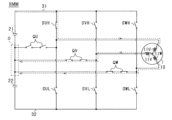
- FIG. 1 is a configuration diagram of a motor control system
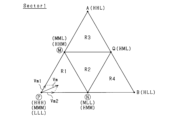
- FIG. 2 is a diagram used to explain the command voltage vector
- FIG. 3 is a diagram used to explain the command voltage vector
- FIG. 4 is a diagram showing a current path during a period in which the output voltage vector HMM is output.
- FIG. 5 is a diagram showing a current path during a period in which the output voltage vector MLL is output.
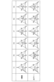
- FIG. 6 is a diagram showing divided areas of limit control
- FIG. 7 is a diagram showing a method of setting an output pattern
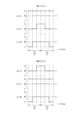
- FIG. 8 is a time chart showing an example of changes in each phase voltage in limit control;
- FIG. 1 is a configuration diagram of a motor control system
- FIG. 2 is a diagram used to explain the command voltage vector
- FIG. 3 is a diagram used to explain the command voltage vector
- FIG. 4 is a diagram showing a current path during a period in which the output voltage vector HMM is output.
- FIG. 5 is a diagram showing a current path during a
- FIG. 9 is a time chart showing an example of changes in each phase voltage in limit control
- FIG. 10 is a time chart showing an example of the transition of each phase voltage in limit control
- FIG. 11 is a time chart showing an example of the transition of each phase voltage in limit control
- FIG. 12 is a time chart showing an example of changes in each phase voltage in limit control
- FIG. 13 is a time chart showing an example of changes in each phase voltage in limit control
- FIG. 14 is a flowchart showing the control procedure performed by the control device
- FIG. 15 is a flowchart showing the control procedure performed by the control device according to the second embodiment
- FIG. 16 is a time chart showing an example of the transition of each phase voltage in limit control
- FIG. 17 is a time chart showing an example of changes in each phase voltage in limit control.
- control device is mounted on an electric vehicle.
- the motor control system includes a rotating electrical machine 10, a battery 20, an inverter 30, and a control device 40.
- the rotating electrical machine 10 is a vehicle-mounted main machine, and is capable of transmitting power to drive wheels (not shown).
- the rotating electric machine 10 is a three-phase synchronous machine, and includes a U-phase winding 11U, a V-phase winding 11V, and a W-phase winding 11W, which are connected in a star shape as stator windings.
- the phase windings 11U, 11V, and 11W are arranged to be shifted by 120 degrees in electrical angle.
- the rotating electric machine 10 is, for example, a permanent magnet synchronous machine.
- the rotating electric machine 10 corresponds to a "driving object".
- the battery 20 is electrically connected to the rotating electrical machine 10 via an inverter 30.
- the battery 20 is an assembled battery configured as a series connection of battery cells, for example, as single batteries.
- a secondary battery such as a lithium ion battery can be used.
- the inter-terminal voltage VH of the battery 20 is, for example, 100 V or more.
- the inverter 30 is a power conversion circuit that converts DC power supplied from the battery 20 into three-phase AC power through a switching operation, and supplies the converted AC power to the rotating electric machine 10.
- a first capacitor 21 and a second capacitor 22 as power storage units are provided on the battery 20 side of the inverter 30.
- the first capacitor 21 and the second capacitor 22 are connected in series.
- a battery 20 is connected in parallel to the series connection body of the first and second capacitors 21 and 22.
- the capacitance of the first capacitor 21 and the capacitance of the second capacitor are the same value.
- the first capacitor 21 and the second capacitor 22 may be provided outside the inverter 30 or may be built into the inverter 30.
- the inverter 30 is a T-type three-level inverter.
- the inverter 30 includes a series connection body of upper arm switches SUH, SVH, SWH and lower arm switches SUL, SVL, SWL for three phases.
- a voltage-controlled semiconductor switching element is used as each switch SUH to SWL, and specifically, an N-channel MOSFET is used. Therefore, the high potential side terminal of each switch SUH to SWL is a drain, and the low potential side terminal is a source.
- Each switch SUH, SVH, SWH, SUL, SVL, SWL has a corresponding body diode DUH, DVH, DWH, DUL, DVL, DWL.
- the source of the U-phase upper arm switch SUH is connected to the drain of the U-phase lower arm switch SUL.
- a connection point between the U-phase upper arm switch SUH and the U-phase lower arm switch SUL is connected to the U-phase input terminal of the rotating electrical machine 10.
- the source of the V-phase upper arm switch SVH is connected to the drain of the V-phase lower arm switch SVL.
- a connection point between the V-phase upper arm switch SVH and the V-phase lower arm switch SVL is connected to the V-phase input terminal of the rotating electric machine 10.
- the source of the W-phase upper arm switch SWH is connected to the drain of the W-phase lower arm switch SWL.
- a connection point between the W-phase upper arm switch SWH and the W-phase lower arm switch SWL is connected to the W-phase input terminal of the rotating electrical machine 10.
- the drains of each of the upper arm switches SUH to SWH are connected by a positive bus bar 31 such as a bus bar.
- the positive side bus bar 31 is connected to the positive terminal of the battery 20 and the first end of the first capacitor.
- the second end of the first capacitor 21 is connected to the first end of the second capacitor 22 via the neutral point O.
- the sources of each of the lower arm switches SUL to SWL are connected by a negative bus bar 32 such as a bus bar.
- the negative side bus bar 32 is connected to the negative terminal of the battery 20 and the second end of the second capacitor.
- the inverter 30 includes clamp switches QU, QV, and QW that conduct and cut off current in both directions.
- voltage-controlled semiconductor switching elements are used as the switches forming each of the clamp switches QU to QW, and specifically, N-channel MOSFETs are used.
- Each of the clamp switches QU to QW has a corresponding body diode DU, DV, and DW.
- the sources of each switch forming the U-phase clamp switch QU are connected to each other.
- the switches that make up the U-phase clamp switch QU one drain is connected to the connection point between the U-phase upper arm switch SUH and the U-phase lower arm switch SUL, and the other drain is connected to the neutral point O. has been done.
- the sources of each switch constituting the V-phase clamp switch QV are connected to each other.
- the switches constituting the V-phase clamp switch QV one drain is connected to the connection point between the V-phase upper arm switch SVH and the V-phase lower arm switch SVL, and the other drain is connected to the neutral point.
- the sources of each switch constituting the W-phase clamp switch QW are connected to each other.
- the switches constituting the W-phase clamp switch QW one drain is connected to the connection point between the W-phase upper arm switch SWH and the W-phase lower arm switch SWL, and the other drain is connected to the neutral point. ing.
- the motor control system includes a first voltage sensor 41, a second voltage sensor 42, a phase current sensor 43, and a rotation angle sensor 44.
- the first voltage sensor 41 detects the voltage between the terminals of the first capacitor 21 .
- the second voltage sensor 42 detects the voltage between the terminals of the second capacitor 22.
- the phase current sensor 43 detects U, V, and W phase currents flowing through the rotating electrical machine 10 . Note that the phase current sensor 43 only needs to be able to detect at least two phase currents among the three phase currents.
- the rotation angle sensor 44 is, for example, a resolver, and detects the rotation angle of the rotating electric machine 10. The detected values of each sensor 41 to 44 are input to the control device 40.
- the control device 40 is mainly composed of a microcomputer 40a (corresponding to a "computer"), and the microcomputer 40a includes a CPU.
- the functions provided by the microcomputer 40a can be provided by software recorded in a physical memory device and a computer that executes it, only software, only hardware, or a combination thereof.
- the microcomputer 40a is provided by an electronic circuit that is hardware, it can be provided by a digital circuit including a large number of logic circuits or an analog circuit.
- the microcomputer 40a executes a program stored in a non-transitory tangible storage medium that serves as a storage unit included in the microcomputer 40a.
- the program includes, for example, a program for processing shown in FIGS. 14, 15, and the like. By executing the program, a method corresponding to the program is executed.
- the storage unit is, for example, a nonvolatile memory. Note that the program stored in the storage unit can be updated via a network such as the Internet, for example.
- the control device 40 generates drive commands to turn on and off each of the switches SUH to SWL and QU to QW of the inverter 30 by space vector modulation control.
- the control device 40 turns on and off the corresponding switches SUH to SWL and QU to QW based on the generated drive command.
- the process of generating drive commands for the switches SUH to SWL and QU to QW by the control device 40 will be described below.
- the control device 40 acquires a command voltage vector for controlling the control amount of the driven object to a command value.
- the control device 40 acquires a command voltage vector Vm for controlling the torque of the rotating electrical machine 10 to the command torque.
- the control device 40 calculates command torque as a manipulated variable for feedback controlling the rotation speed of the rotor of the rotating electric machine 10 to the calculated command rotation speed.
- the rotation speed of the rotor of the rotating electrical machine 10 is calculated based on the detected value of the rotation angle sensor 44.
- the command voltage vector Vm will be explained using FIGS. 2 and 3.
- the command voltage vector Vm is expressed as a spatial voltage vector whose components are U, V, and W phase voltages applied to the rotating electrical machine 10.
- the axes of the U, V, and W phases are shifted by 120 degrees in electrical angle.
- the output voltage vector that can be output by the inverter 30 among the spatial voltage vectors is represented as a component by a set of voltages for each phase.
- Each phase voltage of the output voltage vector is represented by three levels H, M, and L.
- the phase voltage at level H is the phase voltage that is output when the input terminal of each phase and the corresponding upper arm switches SUH to SWH are connected.
- the phase voltage at level M is the phase voltage output when the input terminal of each phase and the corresponding clamp switches QU to QW are connected.
- the phase voltage at level L is the phase voltage output when the input terminal of each phase and the corresponding lower arm switches SUL to SWL are connected.
- the output voltage vector HML represents that the U-phase voltage is at level H, the V-phase voltage is at level M, and the W-phase voltage is at level L.
- phase voltage at level H is VH
- phase voltage at level M is VH/2
- phase voltage at level L is 0.
- Each phase voltage is the potential of the input terminal of each phase when the potential of the negative terminal of the battery 20 is a reference potential (0V).
- the control device 40 specifies the region where the command voltage vector Vm exists.
- the control device 40 specifies the sector and divided area in which the command voltage vector Vm exists. The sectors and divided areas are used to set an output pattern, which will be described later.
- the control device 40 identifies the sector in which the command voltage vector Vm exists based on the electrical angle ⁇ e of the command voltage vector Vm.
- the electrical angle ⁇ e is the angle formed by the command voltage vector Vm and the U-phase axis, and takes a value of 0° to 360°.
- the sign of the electrical angle ⁇ e is positive when rotating to the left (counterclockwise).
- the vector space in which the command voltage vector Vm can exist is divided into six sectors with respect to the electrical angle ⁇ e.
- the control device 40 specifies that the command voltage vector Vm exists in the first sector when 0° ⁇ e ⁇ 60°, and determines that the command voltage vector Vm exists in the second sector when 60° ⁇ e ⁇ 120°. Identify.
- the control device 40 specifies that the command voltage vector Vm exists in the third sector when 120° ⁇ e ⁇ 180°, and determines that the command voltage vector Vm exists in the fourth sector when 180° ⁇ e ⁇ 240°. Identify.
- the control device 40 specifies that the command voltage vector Vm exists in the fifth sector when 240° ⁇ e ⁇ 300°, and specifies that the command voltage vector Vm exists in the sixth sector when 300° ⁇ e ⁇ 360°. Identify.
- a range indicating the first sector is illustratively hatched with dots.
- the first to sixth sectors have an equilateral triangular shape, and each sector is provided with control points A, B, M, N, P, and Q.
- the control point P is the origin in FIG. 2, and is the starting point of the command voltage vector Vm.
- Control points A and B are points provided at the apex of each sector.
- Control point M is a point provided at the midpoint between control point A and control point P.
- Control point N is a point provided at the midpoint between control point B and control point P.
- Control point Q is a point provided at the midpoint between control point A and control point B.
- FIG. 3 shows the relationship between each control point A, B, M, N, P, Q provided for the first sector and each output voltage vector.
- Output voltage vectors whose starting and ending points are control points P are output voltage vectors HHH, MMM, and LLL, and correspond to reactive voltage vectors.
- the output voltage vector having the control point P as the starting point and the control point Q as the ending point is the output voltage vector HML.
- the output voltage vector having the control point P as the starting point and the control point A as the ending point is the output voltage vector HHL.
- the output voltage vector having the control point P as the starting point and the control point B as the ending point is the output voltage vector HLL.
- the output voltage vectors having the control point P as the starting point and the control point M as the ending point are the output voltage vectors HHM and MML.
- the output voltage vectors having the control point P as the starting point and the control point N as the ending point are the output voltage vectors HMM and MLL.
- the relationship between each control point A, B, M, N, P, Q provided for the second to sixth sectors and each output voltage vector is determined.
- the output voltage vector having the control point P as the starting point and the control point Q as the ending point is the output voltage vector MHL.
- the output voltage vector having the control point P as the starting point and the control point A as the ending point is the output voltage vector LHL.
- the output voltage vector having the control point P as the starting point and the control point B as the ending point is the output voltage vector HHL.
- the output voltage vectors having the control point P as the starting point and the control point M as the ending point are the output voltage vectors MHM and LML.
- the output voltage vectors having the control point P as the starting point and the control point N as the ending point are the output voltage vectors HHM and MML.
- the output voltage vector having the control point P as the starting point and the control point Q as the ending point is the output voltage vector LHM.
- the output voltage vector having the control point P as the starting point and the control point A as the ending point is the output voltage vector LHH.
- the output voltage vector having the control point P as the starting point and the control point B as the ending point is the output voltage vector LHL.
- the output voltage vectors having the control point P as the starting point and the control point M as the ending point are the output voltage vectors MHH and LMM.
- the output voltage vectors having the control point P as the starting point and the control point N as the ending point are the output voltage vectors MHM and LML.
- the output voltage vector having the control point P as the starting point and the control point Q as the ending point is the output voltage vector LMH.
- the output voltage vector having the control point P as the starting point and the control point A as the ending point is the output voltage vector LLH.
- the output voltage vector having the control point P as the starting point and the control point B as the ending point is the output voltage vector LHH.
- the output voltage vectors having the control point P as the starting point and the control point M as the ending point are the output voltage vectors MMH and LLM.
- the output voltage vectors having the control point P as the starting point and the control point N as the ending point are the output voltage vectors MHH and LMM.
- the output voltage vector having the control point P as the starting point and the control point Q as the ending point is the output voltage vector MLH.
- the output voltage vector having the control point P as the starting point and the control point A as the ending point is the output voltage vector HLH.
- the output voltage vector having the control point P as the starting point and the control point B as the ending point is the output voltage vector LLH.
- the output voltage vectors having the control point P as the starting point and the control point M as the ending point are the output voltage vectors HMH and MLM.
- the output voltage vectors having the control point P as the starting point and the control point N as the ending point are the output voltage vectors MMH and LLM.
- the output voltage vector having the control point P as the starting point and the control point Q as the ending point is the output voltage vector HLM.
- the output voltage vector having the control point P as the starting point and the control point A as the ending point is the output voltage vector HLL.
- the output voltage vector having the control point P as the starting point and the control point B as the ending point is the output voltage vector HLH.
- the output voltage vectors having the control point P as the starting point and the control point M as the ending point are the output voltage vectors HMM and MLL.
- the output voltage vectors having the control point P as the starting point and the control point N as the ending point are the output voltage vectors HMH and MLM.
- the control device 40 Based on the magnitude of the command voltage vector Vm and the electrical angle ⁇ e, the control device 40 identifies the divided region within the sector where the command voltage vector Vm exists.
- the divided areas are areas defined based on control points A, B, M, N, P, and Q provided for the first to sixth sectors.
- the first divided area R1 of the first to sixth sectors is an area surrounded by an equilateral triangle having the control points P, M, and N as vertices
- the second divided area R2 of the first to sixth sectors is an area surrounded by each control point P, M, and N. This is an area surrounded by an equilateral triangle with control points M, N, and Q as vertices
- the third divided area R3 of the first to sixth sectors is an area surrounded by an equilateral triangle with the control points A, M, and Q as vertices
- the fourth divided area R4 of the first to sixth sectors is This is an area surrounded by an equilateral triangle with control points B, N, and Q as vertices.
- control device 40 may generate information (specifically, map information or numerical formula information) to specify the divided region where the command voltage vector Vm exists.
- the control device 40 sets an output pattern that is a combination of output voltage vectors based on the divided region where the command voltage vector Vm exists.
- the control device 40 includes in the output pattern the output voltage vector corresponding to the control point at the apex of the divided region where the command voltage vector Vm exists. For example, as shown in FIG. 3, when the control device 40 specifies that the command voltage vector Vm exists in the first divided region R1, the control device 40 includes the output voltage vectors corresponding to each control point P, M, and N in the output pattern. .
- the control device 40 decomposes the command voltage vector Vm into output voltage vectors included in the output pattern.
- the control device 40 calculates the output period occupied by one modulation period of the corresponding output voltage vector based on the magnitude of the decomposed output voltage vector.
- the control device 40 generates a drive command to turn on and off each of the switches SUH to SWL and QU to QW of the inverter 30 based on the calculated output period.
- the command voltage vector Vm when it is specified that the command voltage vector Vm exists in the first divided region R1, the command voltage vector Vm is decomposed into output voltage vectors corresponding to each control point M and N.
- Vm1 is a vector obtained by multiplying the output voltage vector corresponding to control point M by ⁇ (0 ⁇ 1)
- Vm2 is a vector obtained by multiplying the output voltage vector corresponding to control point N by ⁇ (0 ⁇ 1). ⁇ 1).
- the larger the coefficient ⁇ the longer the output period of the output voltage vector corresponding to the control point M in one modulation period.
- the larger the coefficient ⁇ the longer the output period of the output voltage vector corresponding to the control point N in one modulation period.
- periods other than the period corresponding to the coefficient ⁇ and the period corresponding to the coefficient ⁇ are set as output periods of the reactive voltage vector.
- the voltage at the neutral point O may change. Therefore, during the output period of the output voltage vector corresponding to each control point M, N, Q, the voltage at the neutral point O may change.
- the output voltage vector corresponding to each control point M, N there are two driving states of each switch SUH to SWL, QU to QW.
- the output voltage vectors corresponding to the control points M and N have a Hi-Mid drive state and a Mid-Lo drive state.
- the Hi-Mid drive state is a drive state in which one of the upper arm switches SUH to SWH and the clamp switches QU to QW is turned on, and each of the lower arm switches SUL to SWL is turned off.
- the Mid-Lo drive state is a drive state in which one of the lower arm switches SUL to SWL and the clamp switches QU to QW is turned on, and each of the upper arm switches SUH to SWH is turned off. .
- the output voltage vectors corresponding to the control point N of the first sector are output voltage vectors HMM and MLL.
- the U phase upper arm switch SUH and the V, W phase clamp switches QV, QW are turned on, and the V, W phase upper arm switches SVH, SWH are turned on.
- the phase lower arm switches SUL to SWL and the U-phase clamp switch QU are turned off.
- the U-phase clamp switch QU and the V, W-phase lower arm switches SVL, SWL are turned on, and each phase upper arm switch SUH to SWH is turned on.
- the U-phase lower arm switch SUL, and the V- and W-phase clamp switches QV and QW are turned off.
- the output voltage vector corresponding to each control point M, N corresponds to a "1st output voltage vector.”
- the direction in which the voltage at the neutral point O changes is opposite between the Hi-Mid drive state and the Mid-Lo drive state.
- the direction in which the voltage at the neutral point O changes is opposite between the output period of the output voltage vector HMM that is in the Hi-Mid drive state and the output period of the output voltage vector MLL that is in the Mid-Lo drive state. Become.
- the current path during the period in which the output voltage vector HMM is output is as follows: first capacitor 21 ⁇ positive bus 31 ⁇ U phase upper arm switch SUH ⁇ U phase winding 11U ⁇ V , W phase winding 11V, 11W ⁇ V, W phase clamp switch QV, QW ⁇ neutral point O. As a result, current flows into the neutral point O, so that the voltage at the neutral point O increases.
- the current path during the period when the output voltage vector MLL is output is as follows: neutral point O ⁇ U-phase clamp switch QU ⁇ U-phase winding 11U ⁇ V, W-phase winding 11V, 11W ⁇ V, W-phase lower arm switches SVL, SWL ⁇ negative side bus 32 ⁇ second capacitor 22. As a result, the current flows out from the neutral point O, so the voltage at the neutral point O decreases.
- the control device 40 acquires neutral point information that is information on at least one of the detection values of the first and second voltage sensors 41 and 42 and the detection value of the phase current sensor 43.
- the neutral point information is the detected values of the first and second voltage sensors 41 and 42 and the detected value of the phase current sensor 43.
- the control device 40 selects either the Hi-Mid drive state or the Mid-Lo drive state based on the neutral point information when output voltage vectors corresponding to the control points M and N are output. do. For example, when the voltage between the terminals of the first capacitor 21 detected by the first voltage sensor 41 is lower than the voltage between the terminals of the second capacitor 22 detected by the second voltage sensor 42, the control device 40 controls the It is determined that the voltage at sex point O is rising. In this case, the control device 40 determines which of the Hi-Mid drive state and the Mid-Lo drive state lowers the voltage at the neutral point O when output voltage vectors corresponding to the control points M and N are output. Select the driving state.
- the control device 40 controls the It is determined that the voltage at sex point O is decreasing. In this case, the control device 40 determines which of the Hi-Mid drive state and the Mid-Lo drive state increases the voltage at the neutral point O when output voltage vectors corresponding to the control points M and N are output. Select the driving state.
- the control device 40 calculates the voltage at the neutral point O based on the detected values of the current sensors 43 for each phase.
- the control device 40 determines whether the voltage at the neutral point O is increasing or decreasing based on the calculated voltage at the neutral point O, and changes the Hi-Mid drive state and the Mid- Select one of the Lo drive states.
- the control device 40 calculates the amount of charge flowing into or out of the neutral point O by integrating the detection values of the phase current sensors 43.
- the control device 40 calculates the voltage at the neutral point O based on the calculated charges flowing into or out of the neutral point O and the capacitances of the first and second capacitors 21 and 22.
- the output period of the output voltage vector corresponding to each control point M, N becomes shorter than when the magnitude of the command voltage vector Vm is small, and the output period of the output voltage vector corresponding to the control point Q
- the output period of the output voltage vector corresponding to the output voltage vector may become longer.
- the output voltage vector corresponding to the control point Q is a larger output voltage vector than the output voltage vector corresponding to each of the control points M and N.
- the neutral point O is connected to one of the phase input terminals of the rotating electric machine 10. In this case, there is a concern that the controllability of the voltage at the neutral point O may deteriorate.
- the output voltage vector corresponding to the control point Q corresponds to the "second output voltage vector.”
- the control device 40 selects and executes either normal control or limited control.
- the normal control is a control in which the output voltage vectors corresponding to the control points at the vertices of the first to fourth divided regions R1 to R4 are set as the output pattern.
- the restriction control is control in which the output voltage vector corresponding to the control point Q is restricted from being set as an output pattern. The restriction control will be explained in detail below.
- FIG. 6 shows divided areas for limit control.
- first, fifth to ninth divided regions R1, R5 to R9 are defined for the first to sixth sectors.
- point G the center of gravity of an equilateral triangle surrounded by control points P, A, and B is shown as point G.
- point G is a point that internally divides line segment PQ at a ratio of 2:1. Note that in FIG. 6, the same reference numerals are given to the configurations shown in FIG. 3 for convenience.
- the fifth divided area R5 of the first to sixth sectors is an area surrounded by a triangle having each control point M, N and point G as vertices.
- the sixth divided area R6 of the first to sixth sectors is an area surrounded by a triangle with each control point B, N and point G as vertices, and the seventh divided area R7 of the first to sixth sectors is This is an area surrounded by a triangle having control points A, M, and point G as vertices.
- the eighth divided region R8 of the first to sixth sectors is an area surrounded by a triangle having control points B, Q and point G as vertices, and the ninth divided region R9 of the first to sixth sectors is This is an area surrounded by a triangle having control points A, Q, and point G as vertices.
- the control device 40 limits inclusion of the output voltage vector corresponding to the control point Q in the output pattern.
- output patterns are set as shown in FIG. 7 for the first, fifth to ninth divided regions R1, R5 to R9.
- the output pattern includes output voltage vectors corresponding to each control point P, M, and N.
- the output pattern includes output voltage vectors corresponding to each control point M, N, and Q.
- the sixth to ninth divided regions R6 to R9 are regions that are in contact with either one of the control points A and B.
- the output voltage vector corresponding to each control point A, B is an output voltage vector larger than the output voltage vector corresponding to each control point M, N.
- the drive state of each switch SUH to SWL, QU to QW is such that the neutral point O and each phase input terminal of the rotating electric machine 10 are not connected. state.
- the output pattern corresponds to any three of each control point A, B, M, and N. Contains the output voltage vector. This restricts the output voltage vector corresponding to the control point Q from being included in the output pattern.
- the output voltage vector corresponding to each control point A, B corresponds to a "3rd output voltage vector.”
- the output voltage corresponding to each control point A, B, M, N is determined depending on which of the sixth to ninth divided regions R6 to R9 the command voltage vector Vm exists.
- the method of setting an output pattern that includes any three output voltage vectors among the vectors is changed. Specifically, when it is specified that the command voltage vector Vm exists in the sixth and seventh divided regions R6 and R7, compared to the case where it is specified that the command voltage vector Vm exists in the eighth and ninth divided regions R8 and R9. Therefore, the output of the rotating electrical machine 10 may be reduced to a low output.
- an output pattern is a combination of an output voltage vector corresponding to one of the control points A and B, an output voltage vector corresponding to the control point M, and an output voltage vector corresponding to the control point N.
- the output pattern is a combination of the output voltage vector corresponding to one of the control points M and N, the output voltage vector corresponding to the control point A, and the output voltage vector corresponding to the control point B.
- the ninth divided region R9 When it is specified that the command voltage vector Vm exists in the ninth divided region R9, an output pattern that is a combination of output voltage vectors corresponding to each control point A, B, and M is set.
- the sixth and seventh divided regions R6 and R7 correspond to a "low output region”
- the eighth and ninth divided regions R8 and R9 correspond to a "high output region”.
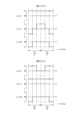
- FIGS. 8 to 13 show examples of changes in each phase voltage during limit control. 8 to 13, (a) shows changes in the U-phase voltage level, (b) shows changes in the V-phase voltage level, and (c) shows changes in the W-phase voltage level. Note that FIGS. 8 to 13 show changes in the voltage levels of each phase in one modulation period Tc. In the transition of each phase voltage level shown in FIGS. 8 to 13, the transition of each phase voltage level in the second half of one modulation period Tc is the inversion of the transition of each phase voltage level in the first half of one modulation period Tc. Ru.
- the first half of one modulation period Tc depends on whether the Hi-Mid drive state or the Mid-Lo drive state is selected.
- the output voltage vectors are output in the following order.
- the Hi-Mid drive state is selected in the first sector
- the output voltage vectors are output in the order of MMM ⁇ HMM ⁇ HHM ⁇ HHH.
- the Hi-Mid drive state is selected in the second sector
- the output voltage vectors are output in the order of MMM ⁇ MHM ⁇ HHM ⁇ HHH. In these cases, the transition of each phase voltage becomes a transition as shown by the solid line in FIG. 8.
- the output voltage vectors are output in the order of MMM ⁇ MML ⁇ MLL ⁇ LLL.
- the output voltage vectors are output in the order of MMM ⁇ MML ⁇ LML ⁇ LLL. In these cases, each phase voltage changes as shown by the broken line in FIG. 8.
- the first half of one modulation period Tc depends on whether the Hi-Mid drive state or the Mid-Lo drive state is selected.
- the output voltage vectors are output in the following order.
- the Hi-Mid drive state is selected in the first sector
- the output voltage vectors are output in the order of HML ⁇ HMM ⁇ HHM.
- the Hi-Mid drive state is selected in the second sector
- the output voltage vectors are output in the order of MHL ⁇ MHM ⁇ HHM. In these cases, the transition of each phase voltage becomes a transition as shown by the solid line in FIG. 9.
- the output voltage vectors are output in the order of HML ⁇ MML ⁇ MLL.
- the output voltage vectors are output in the order of MHL ⁇ MML ⁇ LML. In these cases, each phase voltage changes as shown by the broken line in FIG.
- the first half of one modulation period Tc depends on whether the Hi-Mid drive state or the Mid-Lo drive state is selected.
- the output voltage vectors are output in the following order.
- the Hi-Mid drive state is selected in the first sector
- the output voltage vectors are output in the order of HLL ⁇ HMM ⁇ HHM.
- the Hi-Mid drive state is selected in the second sector
- the output voltage vectors are output in the order of HHL ⁇ HHM ⁇ MHM. In these cases, the transition of each phase voltage becomes a transition as shown by the solid line in FIG. 10.
- the output voltage vectors are output in the order of HLL ⁇ MLL ⁇ MML.
- the output voltage vectors are output in the order of HHL ⁇ MML ⁇ LML. In these cases, the transition of each phase voltage becomes a transition as shown by the broken line in FIG. 10.
- the first half of one modulation period Tc depends on whether the Hi-Mid drive state or the Mid-Lo drive state is selected.
- the output voltage vectors are output in the following order.
- the Hi-Mid drive state is selected in the first sector
- the output voltage vectors are output in the order of HHL ⁇ HHM ⁇ HMM.
- the Hi-Mid drive state is selected in the second sector
- the output voltage vectors are output in the order of LHL ⁇ MHM ⁇ HHM. In these cases, the transition of each phase voltage is as shown by the solid line in FIG. 11.
- the output voltage vectors are output in the order of HHL ⁇ MML ⁇ MLL.
- the output voltage vectors are output in the order of LHL ⁇ LML ⁇ MML. In these cases, the transition of each phase voltage becomes a transition as shown by the broken line in FIG. 11.
- the first half of one modulation period Tc depends on whether the Hi-Mid drive state or the Mid-Lo drive state is selected.
- the output voltage vectors are output in the following order.
- the Hi-Mid drive state is selected in the first sector, the output voltage vectors are output in the order of HMM ⁇ HLL ⁇ HHL.
- the Hi-Mid drive state is selected in the second sector, the output voltage vectors are output in the order of HHM ⁇ HHL ⁇ LHL. In these cases, the transition of each phase voltage is as shown by the solid line in FIG. 12.
- the output voltage vectors are output in the order of MLL ⁇ HLL ⁇ HHL.
- the output voltage vectors are output in the order of MML ⁇ HHL ⁇ LHL. In these cases, the transition of each phase voltage becomes a transition as shown by the broken line in FIG. 12.
- the first half of one modulation period Tc depends on whether the Hi-Mid drive state or the Mid-Lo drive state is selected.
- the output voltage vectors are output in the following order.
- the Hi-Mid drive state is selected in the first sector
- the output voltage vectors are output in the order of HHM ⁇ HHL ⁇ HLL.
- the Hi-Mid drive state is selected in the second sector
- the output voltage vectors are output in the order of MHM ⁇ LHL ⁇ HHL. In these cases, each phase voltage changes as shown by the solid line in FIG. 13.
- the output voltage vectors are output in the order of MML ⁇ HHL ⁇ HLL.
- the output voltage vectors are output in the order of LML ⁇ LHL ⁇ HHL. In these cases, the transition of each phase voltage becomes a transition as shown by the broken line in FIG. 13.
- FIG. 14 shows the control procedure performed by the control device 40. This control is repeatedly executed, for example, at a predetermined control cycle.
- step S10 a command voltage vector Vm is obtained.
- step S11 neutral point information is acquired.
- the detected value of the first voltage sensor 41, the detected value of the second voltage sensor 42, and the detected value of the phase current sensor 43 are acquired as the neutral point information. Note that step S10 corresponds to a "command voltage acquisition section" and step S11 corresponds to a "neutral point information acquisition section.”
- step S12 it is determined whether or not to perform limit control based on the neutral point information.
- the voltage at the neutral point O is calculated based on the detected value of the phase current sensor 43 and the capacitance of the first and second capacitors 21 and 22. Further, for example, if either one of the voltages between the terminals of the first and second capacitors 21 and 22 exceeds the permissible voltage value, it is determined that the voltage at the neutral point O exceeds the permissible range.
- step S12 corresponds to the "determination unit".
- step S13 normal control is performed. In normal control, it is specified which of the first to sixth sectors the command voltage vector Vm exists in, and the command It is specified in which region the voltage vector Vm exists.
- step S14 a set of output voltage vectors corresponding to the control point at the apex of the divided region where the command voltage vector Vm exists is set as an output pattern.
- step S15 the output period of each output voltage vector included in the output pattern is calculated. Specifically, the command voltage vector Vm is decomposed into output voltage vectors included in the output pattern. At this time, if an output voltage vector corresponding to each control point M, N is included, one of the Hi-Mid drive state and the Mid-Lo drive state is selected based on the neutral point information. The command voltage vector is decomposed using the output voltage vector corresponding to the driving state. Based on the size of the decomposed output voltage vector, the output period occupied in one modulation period of the corresponding output voltage vector is calculated. In step S16, a drive command for turning on and off each switch SUH to SWL, QU to QW is generated based on the calculated output period of each output voltage vector. In this embodiment, steps S15 and S16 correspond to a "control unit".
- step S17 the sector in which the command voltage vector Vm exists is specified based on the electrical angle ⁇ e of the command voltage vector Vm. Note that in the following steps S18 to S35, the angle ⁇ s of the command voltage vector Vm within the sector specified in step S17 is used.
- the angle ⁇ s within the sector is the angle formed by the command voltage vector Vm and the line segment PB in FIG. 6, and takes a value of 0° to 60°.
- the angle ⁇ s within the sector is calculated from the electrical angle ⁇ e of the command voltage vector Vm and information on the sector number in which the command voltage vector Vm exists.
- step S18 it is determined whether the command voltage vector Vm exists in the first divided region R1. Determination as to whether or not the command voltage vector Vm exists in the first divided region R1 is based on information (specifically map information or mathematical formula information). If an affirmative determination is made in step S18, the process advances to step S13. On the other hand, if a negative determination is made in step S18, the process advances to step S19.
- step S19 it is determined whether the angle ⁇ s within the sector is smaller than 30°.
- the process of step S19 is a process of determining whether the end point of the command voltage vector Vm exists in the region on the side of each control point B, N with respect to the line segment PQ in FIG. 6 above. If an affirmative determination is made in step S19, the process advances to step S20.
- step S20 it is determined whether
- is the magnitude of the command voltage vector Vm.
- VH/3 is half of the voltage value that can be output as each phase voltage.
- the process of step S20 is a process of determining whether the end point of the command voltage vector Vm exists in a region on the side of each control point A, Q with respect to the line segment BM in FIG. 6. If an affirmative determination is made in step S20, the process advances to step S21. In step S21, it is specified that the command voltage vector Vm exists in the eighth divided region R8. On the other hand, if a negative determination is made in step S20, the process advances to step S22.
- step S22 it is determined whether
- the process of step S22 is a process of determining whether the end point of the command voltage vector Vm exists in a region on the side of each control point M, P with respect to the line segment AN in FIG. If an affirmative determination is made in step S22, the process advances to step S23. In step S23, it is specified that the command voltage vector Vm exists in the fifth divided region R5. On the other hand, if a negative determination is made in step S22, the process advances to step S24. In step S24, it is specified that the command voltage vector Vm exists in the sixth divided region R6.
- step S25 it is determined whether
- the process of step S25 is a process of determining whether the end point of the command voltage vector Vm exists in the area on the control point B, Q side with respect to the line segment AN in FIG. 6 above. If an affirmative determination is made in step S25, the process advances to step S26. In step S26, it is specified that the command voltage vector Vm exists in the ninth divided region R9. On the other hand, if a negative determination is made in step S25, the process advances to step S27.
- step S27 it is determined whether
- the process of step S27 is a process of determining whether the end point of the command voltage vector Vm exists in a region on the side of each control point N, P with respect to the line segment BM in FIG. 6 above. If an affirmative determination is made in step S27, the process advances to step S28. In step S28, it is specified that the command voltage vector Vm exists in the fifth divided region R5. On the other hand, if a negative determination is made in step S27, the process advances to step S29. In step S29, it is specified that the command voltage vector Vm exists in the seventh divided region R7. Note that in this embodiment, the processing in steps S17 to S29 corresponds to the "area specifying section".
- step S30 a set of output voltage vectors corresponding to the eighth divided region R8 is set as an output pattern. Specifically, a set of output voltage vectors corresponding to each control point A, B, and N is set as an output pattern. In this case, the output pattern is restricted from including the output voltage vector corresponding to the control point Q.
- step S31 a set of output voltage vectors corresponding to the fifth divided region R5 is set as an output pattern. Specifically, a set of output voltage vectors corresponding to each control point M, N, and Q is set as an output pattern.
- step S32 a set of output voltage vectors corresponding to the sixth divided region R6 is set as an output pattern. Specifically, a set of output voltage vectors corresponding to each control point B, M, and N is set as an output pattern. In this case, the output pattern is restricted from including the output voltage vector corresponding to the control point Q.
- step S33 a set of output voltage vectors corresponding to the ninth divided region R9 is set as an output pattern. Specifically, a set of output voltage vectors corresponding to each control point A, B, and M is set as an output pattern. In this case, the output pattern is restricted from including the output voltage vector corresponding to the control point Q.
- step S34 If it is determined in step S28 that the command voltage vector Vm exists in the fifth divided region R5, the process proceeds to step S34.
- the process in step S34 is similar to the process in step S31.
- step S35 a set of output voltage vectors corresponding to the seventh divided region R7 is set as an output pattern. Specifically, a set of output voltage vectors corresponding to each control point A, M, and N is set as an output pattern. In this case, the output pattern is restricted from including the output voltage vector corresponding to the control point Q.
- steps S30 to S35 the process advances to step S15. Note that in this embodiment, the processing in steps S30 to S35 corresponds to a "setting section".
- the voltage at the neutral point O changes as a current flows into or out of the neutral point O. obtain. Therefore, during the period in which the output voltage vectors corresponding to the control points M and N are output, the neutral point O is connected to one or two of the phase input terminals of the rotating electric machine 10. , the voltage at the neutral point O may change.
- the output voltage vectors corresponding to the control points M and N have the same voltage applied to each phase input terminal of the rotating electrical machine 10, and the direction of change of the voltage at the neutral point O is opposite.
- the period during which the output voltage vectors corresponding to the control points M and N are output becomes shorter than when the magnitude of the command voltage vector Vm is small.
- the period during which the output voltage vector corresponding to Q is output may become longer.
- the output voltage vector corresponding to the control point Q is a larger output voltage vector than the output voltage vectors corresponding to the control points M and N.
- the neutral point O is connected to any one of the phase input terminals of the rotating electric machine 10, so that the voltage at the neutral point O is not easily controllable. There is a concern that this will decrease.
- an output pattern that is a combination of the output voltage vectors corresponding to the control points A, B, M, and N is set.
- the region where the command voltage vector Vm exists is specified based on the magnitude of the command voltage vector Vm and the electrical angle ⁇ e.
- the existence region includes seventh and ninth divided regions R7 and R9 that are in contact with control point A, and sixth and eighth divided regions R6 and R8 that are in contact with control point B. Then, depending on which of the sixth to ninth divided regions R6 to R9 the command voltage vector Vm exists, an output pattern including output voltage vectors corresponding to each control point A, B, M, and N is generated. Change the setting method.
- an output pattern that is a combination of the output voltage vector corresponding to either one of the control points A and B is set.
- an output pattern is set that includes an output voltage vector corresponding to one of the control points M and N, an output voltage vector corresponding to the control point A, and an output voltage vector corresponding to the control point B.
- the output voltage vector corresponding to one of the control points M and N and the control point A An output pattern that is a combination of the corresponding output voltage vector and the output voltage vector corresponding to control point B is set.
- an output pattern including an output voltage vector corresponding to one of the control points A and B, an output voltage vector corresponding to the control point M, and an output voltage vector corresponding to the control point N is set.
- the size of the average output voltage vector in one modulation period can be increased compared to the case where Thereby, it is possible to cope with an increase in the magnitude of the command voltage vector Vm.
- restriction control it is determined whether or not to perform limit control based on the neutral point information. Specifically, when it is determined that the voltage at the neutral point O exceeds the permissible range, restriction control is performed. On the other hand, if it is not determined that the voltage at the neutral point O exceeds the allowable range, normal control is performed. As a result, limit control is performed in a situation where it is necessary to suppress changes in the voltage at the neutral point O. Therefore, the controllability of the neutral point voltage can be improved while suppressing the controllability of the inverter 30 from decreasing.
- a phase voltage of level H or level L is applied to each phase input terminal of the rotating electric machine 10.
- the phase voltage of level M is not applied to each phase input terminal of the rotating electric machine 10. Therefore, when switching from the drive state corresponding to either one of the output voltage vector corresponding to control point A and the output voltage vector corresponding to control point B to the drive state corresponding to the other, the level M
- Each of the upper and lower arm switches SUH to SWL is turned on and off without a period during which the phase voltage is applied. In this case, there is a concern that the surge voltage generated when each of the upper and lower arm switches SUH to SWL is turned on and off may increase.
- FIG. 15 shows a control procedure performed by the control device 40. This control is repeatedly executed, for example, at a predetermined control cycle.
- step S40 the output voltage vector corresponding to the control point Q is added to the output pattern.
- step S41 switch information regarding the time required for each of the clamp switches QU to QW to be turned on and off is acquired.
- the switch information is information indicating the electrical characteristics of each clamp switch QU to QW, and specifically includes gate threshold voltage, turn-on delay time, turn-off delay time, and the like.
- switch information stored in a storage unit included in the control device 40 may be acquired.
- steps S30 to S35 and step S40 correspond to a "setting section”
- step S41 corresponds to a "switch information acquisition section".
- step S42 the output period of each output voltage vector included in the output pattern is calculated.
- a method for calculating the output period of the output voltage vector corresponding to the control point Q will be described. From the viewpoint of suppressing changes in the voltage at the neutral point O, it is desirable that the output period of the output voltage vector corresponding to the control point Q be shortened. However, if the output period of the output voltage vector corresponding to the control point Q is shorter than the time required to turn each clamp switch QU to QW on and off, the control The output period of the output voltage vector corresponding to point Q ends. In this case, there is a concern that the effect of suppressing the surge voltage generated when each of the upper and lower arm switches SUH to SWL is turned on and off may be reduced.
- the output period of the output voltage vector corresponding to the control point Q is calculated so that it is longer than the time required to turn on and off each of the clamp switches QU to QW.
- the upper limit of the output period of the output voltage vector corresponding to the control point Q may be within half of one modulation period Tc.
- the upper limit of the output period of the output voltage vector corresponding to the control point Q may be 1/6, 1/12, or 1/24 of one modulation period Tc.
- step S42 corresponds to the "calculation section".
- step S43 the control point Drive commands are generated to turn on and off the switches SUH to SWL and QU to QW so as to sandwich the output period of the output voltage vector corresponding to Q.
- step S43 corresponds to the "control unit".
- FIG. 16 shows an example of the transition of each phase voltage level when the command voltage vector Vm is specified to exist in the eighth divided region R8, and FIG. An example of the transition of each phase voltage level when specified is shown. 16(a) to (c) correspond to the previous FIGS. 12(a) to (c), and FIGS. 17(a) to (c) correspond to the previous FIGS. 13(a) to (c). are doing.
- the first half of one modulation period Tc depends on whether the Hi-Mid drive state or the Mid-Lo drive state is selected.
- the output voltage vectors are output in the following order.
- the Hi-Mid drive state is selected in the first sector
- the output voltage vectors are output in the order of HMM ⁇ HLL ⁇ HML ⁇ HHL.
- the Hi-Mid drive state is selected in the second sector
- the output voltage vectors are output in the order of HHM ⁇ HHL ⁇ MHL ⁇ LHL. In these cases, the transition of each phase voltage becomes a transition as shown by the solid line in FIG. 16.
- the output voltage vectors are output in the order of MLL ⁇ HLL ⁇ HML ⁇ HHL.
- the output voltage vectors are output in the order of MML ⁇ HHL ⁇ MHL ⁇ LHL. In these cases, the transition of each phase voltage becomes a transition as shown by the broken line in FIG. 16.
- the first half of one modulation period Tc depends on whether the Hi-Mid drive state or the Mid-Lo drive state is selected.
- the output voltage vectors are output in the following order.
- the Hi-Mid drive state is selected in the first sector
- the output voltage vectors are output in the order of HHM ⁇ HHL ⁇ HML ⁇ HLL.
- the Hi-Mid drive state is selected in the second sector
- the output voltage vectors are output in the order of MHM ⁇ LHL ⁇ MHL ⁇ HHL. In these cases, the transition of each phase voltage becomes a transition as shown by the solid line in FIG. 17.
- the output voltage vectors are output in the order of MML ⁇ HHL ⁇ HML ⁇ HLL.
- the output voltage vectors are output in the order of LML ⁇ LHL ⁇ MHL ⁇ HHL. In these cases, each phase voltage changes as shown by the broken line in FIG. 17.
- the output voltage vector corresponding to the control point Q is added to the output pattern.
- the output pattern includes an output voltage vector corresponding to either control point M or N, an output voltage vector corresponding to control point A, an output voltage vector corresponding to control point B, and an output voltage vector corresponding to control point Q. and an output voltage vector corresponding to .
- Switch information regarding the time required to turn on and off each clamp switch QU to QW is acquired. Based on the switch information, the output period of the output voltage vector corresponding to the control point Q is set so that the output period of the output voltage vector corresponding to the control point Q is longer than the time required to turn on and off each clamp switch QU to QW. is calculated. Thereby, it is possible to accurately secure a period from when the output voltage vector corresponding to the control point Q is output until each of the switches SUH to SWL and QU to QW is actually turned on and off. Therefore, it is possible to accurately reduce the surge voltage that occurs when each of the upper and lower arm switches SUH to SWL is turned on and off.
- the control device 40 acquires only one of them as the neutral point information. You can. For example, the control device 40 may acquire only the detection values of the first and second voltage sensors 41 and 42 among the detection values of the first and second voltage sensors 41 and 42 and the detection values of the phase current sensor 43. good. In this case, the control device 40 may calculate each phase current based on the detected values of the first and second voltage sensors 41 and 42. The control device 40 determines the neutral point O based on each phase current calculated using the detected values of the first and second voltage sensors 41 and 42 and the capacitances of the first and second capacitors 21 and 22. You may also calculate the voltage of Thereby, the processes of steps S10 and S15 can be performed without using the detected value of the phase current sensor 43.
- the divided regions of the restriction control are not limited to the first, fifth to ninth divided regions R1, R5 to R9 shown in FIG. 6 above.
- the divided area may be changed by changing the ratio at which the line segment PQ is internally divided by the point G.
- point G instead of point G being a point that internally divides line segment PQ at a ratio of 2:1, it may be changed to a point that internally divides line segment PQ at a ratio of 3:1.
- the eighth and ninth divided regions R8 and R9 are reduced compared to the first embodiment, and the sixth and seventh divided regions R6 and R7 are enlarged compared to the first embodiment.
- the divided area to be set is widened. Therefore, even when the magnitude of the command voltage vector Vm is large, the period during which the Hi-Mid drive state and the Mid-Lo drive state can be selected can be made longer than in the first embodiment.
- step S19, S20, S22, S25, and S27 it is preferable to change the processing in steps S19, S20, S22, S25, and S27.
- information for example, map information
- the command voltage vector It is preferable to perform processing to identify the divided area where Vm exists.
- the drive target of the inverter 30 is not limited to the rotating electric machine 10 in which each phase winding 11U, 11V, 11W is connected in a star shape, but also a rotating electric machine in which each phase winding 11U, 11V, 11W is connected in a delta connection. good.
- the object to be driven is not limited to a rotating electric machine, but may be any other load having a three-phase winding.
- the inverter 30 may be a neutral point clamp type 3-level inverter instead of the T-type 3-level inverter.
- the semiconductor switches that constitute the inverter are not limited to N-channel MOSFETs, and may be, for example, IGBTs.
- the high potential side terminal of the switch is the collector, and the low potential side terminal is the emitter.
- a freewheel diode may be connected in antiparallel to each switch.
- control unit and the method described in the present disclosure are implemented by a dedicated computer provided by configuring a processor and memory programmed to perform one or more functions embodied by a computer program. May be realized.
- the controller and techniques described in this disclosure may be implemented by a dedicated computer provided by a processor configured with one or more dedicated hardware logic circuits.
- the control unit and the method described in the present disclosure may be implemented using a combination of a processor and memory programmed to perform one or more functions and a processor configured by one or more hardware logic circuits. It may be implemented by one or more dedicated computers configured.
- the computer program may also be stored as instructions executed by a computer on a computer-readable non-transitory tangible storage medium.
Landscapes
- Engineering & Computer Science (AREA)
- Power Engineering (AREA)
- Inverter Devices (AREA)
- Control Of Ac Motors In General (AREA)
Abstract
Description
3相交流電圧が印加されることにより駆動される駆動対象と、
前記駆動対象の各相を、前記第1蓄電部の正極側、前記第1蓄電部の負極側及び前記第2蓄電部の正極側の間の中性点、及び前記第2蓄電部の負極側のうちいずれかに接続する3相分のスイッチを有する3レベルインバータと、を備えるシステムに適用される3レベルインバータの制御装置において、
前記第1,第2蓄電部の電圧及び前記駆動対象の各相に流れる電流のうち少なくとも一方の情報である中性点情報を取得する中性点情報取得部と、
前記駆動対象の制御量を指令値に制御するための指令電圧ベクトルを取得する指令電圧取得部と、
前記指令電圧ベクトルに基づいて、前記3レベルインバータが出力可能な出力電圧ベクトルの組み合わせである出力パターンを設定する設定部と、
前記出力パターンに含まれる前記出力電圧ベクトルに基づいて、前記スイッチをオンオフする制御部と、を備え、
前記スイッチの駆動状態が、前記駆動対象の各相のうちいずれか1相又は2相と、前記中性点とを接続する駆動状態となり、かつ、同一の前記出力電圧ベクトルに対して異なる前記スイッチの駆動状態が2つ存在する前記出力電圧ベクトルを第1出力電圧ベクトルとし、
前記スイッチの駆動状態が、前記駆動対象の各相のうちいずれか1相と、前記中性点とを接続する駆動状態となり、かつ、前記第1出力電圧ベクトルの大きさよりも大きな前記出力電圧ベクトルを第2出力電圧ベクトルとし、
前記制御部は、前記第1出力電圧ベクトルが出力される場合に、前記中性点情報に基づいて、2つの前記スイッチの駆動状態のうちいずれか一方を選択し、
前記設定部は、前記第2出力電圧ベクトルを、前記出力パターンに含むことを制限する。
以下、本開示に係る制御装置を具体化した第1実施形態について、図面を参照しつつ説明する。本実施形態において制御装置は、電気自動車に搭載されている。
以下、第2実施形態について、第1実施形態との相違点を中心に図面を参照しつつ説明する。
なお、上記実施形態は、以下のように変更して実施してもよい。
Claims (6)
- 直列接続された第1蓄電部(21)及び第2蓄電部(22)と、
3相交流電圧が印加されることにより駆動される駆動対象(10)と、
前記駆動対象の各相を、前記第1蓄電部の正極側、前記第1蓄電部の負極側及び前記第2蓄電部の正極側の間の中性点、及び前記第2蓄電部の負極側のうちいずれかに接続する3相分のスイッチ(SUH~SWL,QU~QW)を有する3レベルインバータ(30)と、を備えるシステムに適用される3レベルインバータの制御装置(40)において、
前記第1,第2蓄電部の電圧及び前記駆動対象の各相に流れる電流のうち少なくとも一方の情報である中性点情報を取得する中性点情報取得部と、
前記駆動対象の制御量を指令値に制御するための指令電圧ベクトルを取得する指令電圧取得部と、
前記指令電圧ベクトルに基づいて、前記3レベルインバータが出力可能な出力電圧ベクトルの組み合わせである出力パターンを設定する設定部と、
前記出力パターンに含まれる前記出力電圧ベクトルに基づいて、前記スイッチをオンオフする制御部と、を備え、
前記スイッチの駆動状態が、前記駆動対象の各相のうちいずれか1相又は2相と、前記中性点とを接続する駆動状態となり、かつ、同一の前記出力電圧ベクトルに対して異なる前記スイッチの駆動状態が2つ存在する前記出力電圧ベクトルを第1出力電圧ベクトルとし、
前記スイッチの駆動状態が、前記駆動対象の各相のうちいずれか1相と、前記中性点とを接続する駆動状態となり、かつ、前記第1出力電圧ベクトルの大きさよりも大きな前記出力電圧ベクトルを第2出力電圧ベクトルとし、
前記制御部は、前記第1出力電圧ベクトルが出力される場合に、前記中性点情報に基づいて、2つの前記スイッチの駆動状態のうちいずれか一方を選択し、
前記設定部は、前記第2出力電圧ベクトルを、前記出力パターンに含むことを制限する3レベルインバータの制御装置。 - 前記駆動対象は、前記3レベルインバータに電気的に接続される巻線(11U,11V,11W)を有する回転電機(10)であり、
前記指令電圧ベクトルの大きさ及び電気角に基づいて、前記指令電圧ベクトルの存在領域を特定する領域特定部を備え、
前記スイッチの駆動状態が、前記駆動対象の各相と、前記中性点とが接続されない駆動状態となり、かつ、前記第1出力電圧ベクトルの大きさよりも大きな前記出力電圧ベクトルを第3出力電圧ベクトルとし、
前記存在領域には、前記第3出力電圧ベクトルの終点に接する高出力領域及び低出力領域が含まれており、
前記設定部は、
前記指令電圧ベクトルが前記高出力領域に存在すると特定された場合に、1つの前記第1出力電圧ベクトルと、2つの前記第3出力電圧ベクトルとの組み合わせである前記出力パターンを設定し、
前記指令電圧ベクトルが前記低出力領域に存在すると特定された場合に、2つの前記第1出力電圧ベクトルと、1つの前記第3出力電圧ベクトルとの組み合わせである前記出力パターンを設定する請求項1に記載の3レベルインバータの制御装置。 - 前記設定部は、前記指令電圧ベクトルが前記高出力領域に存在すると特定された場合に、前記出力パターンに前記第2出力電圧ベクトルを追加し、
前記制御部は、
前記第3出力電圧ベクトルが出力される期間では、前記スイッチの駆動状態を、前記駆動対象の各相と、前記第1蓄電部の正極側又は前記第2蓄電部の負極側とが接続される駆動状態とし、
前記出力パターンに前記第2出力電圧ベクトルが追加された場合、2つの前記第3出力電圧ベクトルのうち、一方に対応する前記スイッチの駆動状態から、他方に対応する前記スイッチの駆動状態へと前記スイッチをオンオフする間において、前記第2出力電圧ベクトルに対応する前記スイッチの駆動状態を挟むように、前記スイッチをオンオフする請求項2に記載の3レベルインバータの制御装置。 - 前記スイッチのゲート閾値電圧、ターンオン遅延時間及びターンオフ遅延時間のうち少なくとも1つであるスイッチ情報を取得するスイッチ情報取得部と、
前記スイッチ情報に基づいて、前記第2出力電圧ベクトルの出力期間が前記スイッチのオンオフに要する時間よりも長くなるように、前記第2出力電圧ベクトルの出力期間を算出する算出部と、を備える請求項3に記載の3レベルインバータの制御装置。 - 前記中性点情報に基づいて、前記中性点の電圧が許容範囲を超えているか否かを判定する判定部を備え、
前記設定部は、前記中性点の電圧が許容範囲を超えていると判定された場合に、前記第2出力電圧ベクトルが前記出力パターンに含まれることを制限するとともに、前記中性点の電圧が許容範囲を超えていると判定されない場合に、前記第2出力電圧ベクトルが前記出力パターンに含まれることを制限しない請求項1~4のいずれか1項に記載の3レベルインバータの制御装置。 - 直列接続された第1蓄電部(21)及び第2蓄電部(22)と、
3相交流電圧が印加されることにより駆動される駆動対象(10)と、
前記駆動対象の各相を、前記第1蓄電部の正極側、前記第1蓄電部の負極側及び前記第2蓄電部の正極側の間の中性点、及び前記第2蓄電部の負極側のうちいずれかに接続する3相分のスイッチ(SUH~SWL,QU~QW)を有する3レベルインバータ(30)と、
コンピュータ(40a)と、を備えるシステムに適用されるプログラムにおいて、
前記第1,第2蓄電部の電圧及び前記駆動対象の各相に流れる電流のうち少なくとも一方の情報である中性点情報を取得する中性点情報取得ステップと、
前記駆動対象の制御量を指令値に制御するための指令電圧ベクトルを取得する指令電圧取得ステップと、
前記指令電圧ベクトルに基づいて、前記3レベルインバータが出力可能な出力電圧ベクトルの組み合わせである出力パターンを設定する設定ステップと、
前記出力パターンに含まれる前記出力電圧ベクトルに基づいて、前記スイッチをオンオフする制御ステップと、を前記コンピュータに実行させ、
前記スイッチの駆動状態が、前記駆動対象の各相のうちいずれか1相又は2相と、前記中性点とを接続する駆動状態となり、かつ、同一の前記出力電圧ベクトルに対して異なる前記スイッチの駆動状態が2つ存在する前記出力電圧ベクトルを第1出力電圧ベクトルとし、
前記スイッチの駆動状態が、前記駆動対象の各相のうちいずれか1相と、前記中性点とを接続する駆動状態となり、かつ、前記第1出力電圧ベクトルの大きさよりも大きな前記出力電圧ベクトルを第2出力電圧ベクトルとし、
前記制御ステップは、前記第1出力電圧ベクトルが出力される場合に、前記中性点情報に基づいて、2つの前記スイッチの駆動状態のうちいずれか一方を選択する処理を含み、
前記設定ステップは、前記第2出力電圧ベクトルを、前記出力パターンに含むことを制限する処理を含むプログラム。
Priority Applications (3)
| Application Number | Priority Date | Filing Date | Title |
|---|---|---|---|
| DE112023002395.6T DE112023002395T5 (de) | 2022-05-24 | 2023-04-28 | Steuerungsvorrichtung für einendrei-pegel-wechselrichter und ein programm |
| CN202380042264.0A CN119256484A (zh) | 2022-05-24 | 2023-04-28 | 三电平逆变器的控制装置和程序 |
| US18/958,827 US20250088131A1 (en) | 2022-05-24 | 2024-11-25 | Control device for three-level inverter, storage medium, and control method for three-level inverter |
Applications Claiming Priority (2)
| Application Number | Priority Date | Filing Date | Title |
|---|---|---|---|
| JP2022-084852 | 2022-05-24 | ||
| JP2022084852A JP7609125B2 (ja) | 2022-05-24 | 2022-05-24 | 3レベルインバータの制御装置、プログラム、及び3レベルインバータの制御方法 |
Related Child Applications (1)
| Application Number | Title | Priority Date | Filing Date |
|---|---|---|---|
| US18/958,827 Continuation US20250088131A1 (en) | 2022-05-24 | 2024-11-25 | Control device for three-level inverter, storage medium, and control method for three-level inverter |
Publications (1)
| Publication Number | Publication Date |
|---|---|
| WO2023228680A1 true WO2023228680A1 (ja) | 2023-11-30 |
Family
ID=88919183
Family Applications (1)
| Application Number | Title | Priority Date | Filing Date |
|---|---|---|---|
| PCT/JP2023/016875 Ceased WO2023228680A1 (ja) | 2022-05-24 | 2023-04-28 | 3レベルインバータの制御装置及びプログラム |
Country Status (5)
| Country | Link |
|---|---|
| US (1) | US20250088131A1 (ja) |
| JP (1) | JP7609125B2 (ja) |
| CN (1) | CN119256484A (ja) |
| DE (1) | DE112023002395T5 (ja) |
| WO (1) | WO2023228680A1 (ja) |
Families Citing this family (1)
| Publication number | Priority date | Publication date | Assignee | Title |
|---|---|---|---|---|
| US20250158552A1 (en) * | 2023-11-10 | 2025-05-15 | GM Global Technology Operations LLC | Mixed chemistry battery pack power transfer using a multilevel t-type inverter |
Citations (4)
| Publication number | Priority date | Publication date | Assignee | Title |
|---|---|---|---|---|
| JPH11122944A (ja) * | 1997-10-15 | 1999-04-30 | Toshiba Corp | Npc変換器の制御装置 |
| JP2014033609A (ja) * | 2012-07-31 | 2014-02-20 | General Electric Co <Ge> | 無変圧器無停電電源装置のための知的レベル移行システムおよび方法 |
| JP2020025451A (ja) * | 2018-08-01 | 2020-02-13 | 株式会社安川電機 | 電力変換装置及び制御方法 |
| WO2021038698A1 (ja) * | 2019-08-26 | 2021-03-04 | 株式会社デンソー | インバータ |
Family Cites Families (2)
| Publication number | Priority date | Publication date | Assignee | Title |
|---|---|---|---|---|
| JPH0937592A (ja) | 1995-07-21 | 1997-02-07 | Toyo Electric Mfg Co Ltd | 3レベルインバータのpwm制御方法および制御装置 |
| WO2019060695A1 (en) | 2017-09-22 | 2019-03-28 | Kite Pharma, Inc. | CHIMERIC POLYPEPTIDES AND USES THEREOF |
-
2022
- 2022-05-24 JP JP2022084852A patent/JP7609125B2/ja active Active
-
2023
- 2023-04-28 WO PCT/JP2023/016875 patent/WO2023228680A1/ja not_active Ceased
- 2023-04-28 DE DE112023002395.6T patent/DE112023002395T5/de active Pending
- 2023-04-28 CN CN202380042264.0A patent/CN119256484A/zh active Pending
-
2024
- 2024-11-25 US US18/958,827 patent/US20250088131A1/en active Pending
Patent Citations (4)
| Publication number | Priority date | Publication date | Assignee | Title |
|---|---|---|---|---|
| JPH11122944A (ja) * | 1997-10-15 | 1999-04-30 | Toshiba Corp | Npc変換器の制御装置 |
| JP2014033609A (ja) * | 2012-07-31 | 2014-02-20 | General Electric Co <Ge> | 無変圧器無停電電源装置のための知的レベル移行システムおよび方法 |
| JP2020025451A (ja) * | 2018-08-01 | 2020-02-13 | 株式会社安川電機 | 電力変換装置及び制御方法 |
| WO2021038698A1 (ja) * | 2019-08-26 | 2021-03-04 | 株式会社デンソー | インバータ |
Also Published As
| Publication number | Publication date |
|---|---|
| JP2023172786A (ja) | 2023-12-06 |
| CN119256484A (zh) | 2025-01-03 |
| DE112023002395T5 (de) | 2025-03-06 |
| JP7609125B2 (ja) | 2025-01-07 |
| US20250088131A1 (en) | 2025-03-13 |
Similar Documents
| Publication | Publication Date | Title |
|---|---|---|
| US9871483B2 (en) | Controller for rotary electric machine drive apparatus | |
| JP6683514B2 (ja) | 電力変換装置 | |
| CN111201705B (zh) | 旋转电机的控制装置 | |
| US12132395B2 (en) | Rotating electrical machine control device | |
| JP2018196179A (ja) | 回転電機の制御装置 | |
| JP7354962B2 (ja) | インバータの制御装置、プログラム | |
| JP7544656B2 (ja) | モータ制御装置 | |
| US20250088131A1 (en) | Control device for three-level inverter, storage medium, and control method for three-level inverter | |
| JP7354953B2 (ja) | 電力変換装置の制御装置、プログラム | |
| JP5515787B2 (ja) | 回転電機制御システム | |
| JP7564615B2 (ja) | 回転電機の制御装置、プログラム、回転電機の制御方法 | |
| JP7759617B2 (ja) | 回転電機の制御装置、及びプログラム | |
| US20260019022A1 (en) | Control apparatus for three-level inverter | |
| JP7816270B2 (ja) | 電力変換装置、プログラム、電力変換装置の制御方法 | |
| JP7835196B2 (ja) | インバータ制御装置、プログラム | |
| WO2025047246A1 (ja) | 3レベルインバータの制御装置、及びプログラム | |
| JP7367628B2 (ja) | インバータの制御装置 | |
| EP4213373B1 (en) | Control device for rotating electrical machine | |
| JP7294982B2 (ja) | 電動機制御装置 | |
| JP2019047688A (ja) | モータ駆動装置 | |
| JP7144197B2 (ja) | 回転電機の制御装置 | |
| WO2025142363A1 (ja) | 回転電機の制御装置、プログラム、及び回転電機の制御方法 | |
| WO2025142364A1 (ja) | 回転電機の制御装置、プログラム、及び回転電機の制御方法 | |
| WO2025177759A1 (ja) | インバータ制御装置、プログラム、インバータ制御方法 | |
| WO2025142362A1 (ja) | 回転電機の制御装置、プログラム、及び回転電機の制御方法 |
Legal Events
| Date | Code | Title | Description |
|---|---|---|---|
| 121 | Ep: the epo has been informed by wipo that ep was designated in this application |
Ref document number: 23811558 Country of ref document: EP Kind code of ref document: A1 |
|
| WWE | Wipo information: entry into national phase |
Ref document number: 202380042264.0 Country of ref document: CN |
|
| WWE | Wipo information: entry into national phase |
Ref document number: 202417096402 Country of ref document: IN |
|
| WWE | Wipo information: entry into national phase |
Ref document number: 112023002395 Country of ref document: DE |
|
| WWP | Wipo information: published in national office |
Ref document number: 202380042264.0 Country of ref document: CN |
|
| WWP | Wipo information: published in national office |
Ref document number: 112023002395 Country of ref document: DE |
|
| 122 | Ep: pct application non-entry in european phase |
Ref document number: 23811558 Country of ref document: EP Kind code of ref document: A1 |