WO2023228545A1 - 固体撮像装置およびドライバ回路 - Google Patents
固体撮像装置およびドライバ回路 Download PDFInfo
- Publication number
- WO2023228545A1 WO2023228545A1 PCT/JP2023/012142 JP2023012142W WO2023228545A1 WO 2023228545 A1 WO2023228545 A1 WO 2023228545A1 JP 2023012142 W JP2023012142 W JP 2023012142W WO 2023228545 A1 WO2023228545 A1 WO 2023228545A1
- Authority
- WO
- WIPO (PCT)
- Prior art keywords
- current
- section
- driver
- drive
- signal
- Prior art date
- Legal status (The legal status is an assumption and is not a legal conclusion. Google has not performed a legal analysis and makes no representation as to the accuracy of the status listed.)
- Ceased
Links
Images





Classifications
-
- H—ELECTRICITY
- H04—ELECTRIC COMMUNICATION TECHNIQUE
- H04N—PICTORIAL COMMUNICATION, e.g. TELEVISION
- H04N25/00—Circuitry of solid-state image sensors [SSIS]; Control thereof
- H04N25/70—SSIS architectures; Circuits associated therewith
- H04N25/76—Addressed sensors, e.g. MOS or CMOS sensors
-
- H—ELECTRICITY
- H04—ELECTRIC COMMUNICATION TECHNIQUE
- H04N—PICTORIAL COMMUNICATION, e.g. TELEVISION
- H04N25/00—Circuitry of solid-state image sensors [SSIS]; Control thereof
- H04N25/70—SSIS architectures; Circuits associated therewith
- H04N25/709—Circuitry for control of the power supply
-
- H—ELECTRICITY
- H04—ELECTRIC COMMUNICATION TECHNIQUE
- H04N—PICTORIAL COMMUNICATION, e.g. TELEVISION
- H04N25/00—Circuitry of solid-state image sensors [SSIS]; Control thereof
- H04N25/70—SSIS architectures; Circuits associated therewith
- H04N25/76—Addressed sensors, e.g. MOS or CMOS sensors
- H04N25/77—Pixel circuitry, e.g. memories, A/D converters, pixel amplifiers, shared circuits or shared components
-
- H—ELECTRICITY
- H04—ELECTRIC COMMUNICATION TECHNIQUE
- H04N—PICTORIAL COMMUNICATION, e.g. TELEVISION
- H04N25/00—Circuitry of solid-state image sensors [SSIS]; Control thereof
- H04N25/70—SSIS architectures; Circuits associated therewith
- H04N25/76—Addressed sensors, e.g. MOS or CMOS sensors
- H04N25/779—Circuitry for scanning or addressing the pixel array
-
- H—ELECTRICITY
- H04—ELECTRIC COMMUNICATION TECHNIQUE
- H04N—PICTORIAL COMMUNICATION, e.g. TELEVISION
- H04N25/00—Circuitry of solid-state image sensors [SSIS]; Control thereof
- H04N25/70—SSIS architectures; Circuits associated therewith
- H04N25/76—Addressed sensors, e.g. MOS or CMOS sensors
- H04N25/7795—Circuitry for generating timing or clock signals
Definitions
- the present technology relates to a driver circuit and a solid-state imaging device. Specifically, the present technology relates to a current-driven driver circuit and a solid-state imaging device.
- a solid-state imaging device is provided with a driver circuit that drives pixels in order to realize an imaging operation.
- This driver circuit includes a plurality of drivers each having the same driving force.
- As such a driver circuit there is a configuration in which a bias voltage is distributed from a bias circuit to a plurality of local blocks via long wiring (for example, see Patent Document 1).
- the transistor that generates the current that causes the driver circuit to operate as a current driver is voltage-driven based on the power supply voltage. For this reason, as the number of wiring lines for supplying the power supply voltage increases, the IR drop increases, and the gate-source voltage of the transistor decreases, leading to a possibility that the slew rate decreases.
- This technology was created in view of this situation, and its purpose is to improve the uniformity of driving of the driver circuit.
- the solid-state imaging device includes a generation section and a current drive section that is driven by a shunt current obtained by branching the current generated by the current generation section and generates a drive signal for the pixel based on a control signal. This brings about the effect that a pixel drive signal is generated based on current drive.
- the current generation section may control the current based on the control signal. This brings about the effect of being able to cope with an increase or decrease in the number of current drive units driven simultaneously while maintaining a constant slew rate of the current drive units.
- control signal may include designation information that designates a current drive unit to be selected when driving the pixel. This brings about the effect that the current driving section that drives the pixel is selected.
- the designation information may be an address assigned to each of the current drive units. This brings about the effect that the current drive section that generates the drive signal when driving the pixel is specified.
- control signal may include the addresses for the number of the current drive units that are simultaneously driven, and a signal that is toggled according to the number of the current drive units that are simultaneously driven. good. This brings about the effect of specifying the current drive units that are driven at the same time.
- the current generating section may control the current based on the number of the current driving sections that are simultaneously driven, which is extracted from the control signal. This brings about the effect that the current used to drive the current drive unit is controlled based on internal information generated within the solid-state imaging device.
- the current generating section may control the current based on a counter output of a signal toggled according to the number of the current driving sections that are simultaneously driven. This brings about the effect that the current is controlled according to the number of current drive units that are simultaneously driven.
- the current drive units each specified by the addresses corresponding to the counter output may be simultaneously current-driven based on the current controlled by the counter output. This brings about the effect that a plurality of current drive units designated by the control signal are simultaneously current driven.
- the voltage driving section includes a voltage driving section that is supplied with a second power supply voltage different from a first power supply voltage that is supplied to the current generating section and generates a drive signal for the pixel based on the control signal;
- the current driving section and the voltage driving section may further include an output terminal provided in common. This brings about the effect that a drive signal is generated by switching from a low voltage power source to a high voltage power source when driving the transistor.
- the current drive unit includes a first switching element having one end connected to the output terminal
- the voltage drive unit includes a second switching element having one end connected to the output terminal.
- the first switching element may have its other end connected to the current terminal of the current generating section
- the second switching element may have its other end supplied with the second power supply voltage.
- a plurality of the current driving sections may be provided, and the current generating section may be shared by the plurality of current driving sections. This brings about the effect that a plurality of current drive units are current-driven based on the current generated by one current generation unit.
- the current driving section may be connected in parallel to the current generating section. This brings about the effect that the current generated by one current generating section is divided into a plurality of current driving sections.
- the voltage driving section may be provided corresponding to the current driving section, and the second power supply voltage may be supplied to the voltage driving section in parallel. This brings about the effect that the second power supply voltage is supplied to the plurality of voltage drive units.
- the current driving section includes a transistor, a mirror current generated based on a current mirror operation of the current generating section is input to a source of the transistor, and the control signal is applied to a gate of the transistor. may be entered. This brings about the effect that the transistor is current-driven based on the mirror current generated by the current generation section.
- the first aspect may further include a slew rate control section that controls a slew rate of the current drive section based on control of a mirror current generated based on a current mirror operation of the current generation section. good. This brings about the effect that the slew rate of the drive signal is controlled based on the mirror current generated by the current generation section.
- a second aspect includes a current generation unit that generates a current, and a current drive that is driven by a shunt current obtained by dividing the current generated by the current generation unit and generates a drive signal for a transistor based on a control signal.
- a driver circuit comprising: a driver circuit; This brings about the effect that a transistor drive signal is generated based on current drive.
- FIG. 1 is a block diagram showing a configuration example of a solid-state imaging device according to a first embodiment.
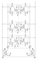
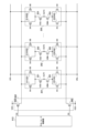
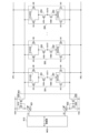
- FIG. FIG. 2 is a circuit diagram showing a configuration example of a driver circuit according to the first embodiment.
- FIG. 2 is a block diagram showing a configuration example of a switching control section and a power supply of the driver circuit according to the first embodiment.
- FIG. 3 is a circuit diagram showing a configuration example of a switching control section of the driver circuit according to the first embodiment.
- FIG. 2 is a circuit diagram showing a configuration example of a logic circuit used to generate a control signal of the driver circuit according to the first embodiment.
- 5 is a timing chart showing the operation of the driver circuit according to the first embodiment.
- FIG. 3 is a diagram showing an example of a slew rate of the driver circuit according to the first embodiment.
- FIG. 3 is a diagram showing an example of the layout of wiring used for current driving of the driver circuit according to the first embodiment.
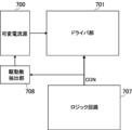
- FIG. 7 is a block diagram showing a configuration example of a driver circuit according to a second embodiment.
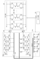
- FIG. 7 is a circuit diagram showing a configuration example of a driver circuit according to a second embodiment.
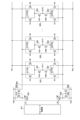
- FIG. 7 is a circuit diagram showing a first example of a driver circuit according to a third embodiment.
- FIG. 7 is a circuit diagram showing a second example of a driver circuit according to a third embodiment.
- FIG. 7 is a circuit diagram showing a third example of a driver circuit according to a third embodiment.
- FIG. 7 is a circuit diagram showing a third example of a driver circuit according to a third embodiment.
- FIG. 7 is a circuit diagram showing a configuration example of a driver circuit according to a fourth embodiment.
- FIG. 1 is a block diagram showing a schematic configuration example of a vehicle control system.
- FIG. 3 is an explanatory diagram showing an example of an installation position of an imaging unit.
- First embodiment (example where multiple drivers are driven based on current generated by a current source) 2.
- Second embodiment (an example of controlling the current generated by a current source according to the number of drivers driven simultaneously) 3.
- Third embodiment (example of changing the slew rate of the drive signal output from the driver based on current control of the current source) 4.
- Fourth embodiment (example where current sources are distributed and arranged between drivers) 5.
- FIG. 1 is a block diagram showing a configuration example of a solid-state imaging device according to a first embodiment.
- a solid-state imaging device 100 includes a pixel array section 101, a vertical drive circuit 102, a horizontal drive circuit 103, a control circuit 104, a column signal processing circuit 105, and an output circuit 106.
- the pixel array section 101 includes a plurality of pixels 111.
- the pixels 111 are arranged in a matrix in the row direction and column direction.
- Each pixel 111 includes a photodiode and a pixel transistor that performs photoelectric conversion.
- the pixel transistors may include, for example, a transfer transistor, a reset transistor, a selection transistor, and an amplification transistor.
- the pixel array section 101 includes a pixel drive line 121 and a vertical signal line 122.
- the pixel drive line 121 transmits a drive signal for driving each pixel 111 in the row direction.
- the vertical signal line 122 transmits the pixel signal read from each pixel 111 in the column direction.
- the drive signal that drives each pixel 111 may include a transfer signal that drives a transfer transistor, a reset signal that drives a reset transistor, and a row selection signal that drives a selection transistor.
- the vertical drive circuit 102 drives the pixels 111 row by row via the vertical signal line 122.
- the vertical drive circuit 102 sequentially selectively scans each pixel 111 of the pixel array section 101 in the column direction in row units. Thereby, a pixel signal based on a signal charge generated according to the amount of light received by each pixel 111 is supplied to the column signal processing circuit 105 via the vertical signal line 122.
- the vertical drive circuit 102 includes a current source 112 and a driver 113.
- the driver 113 can be provided for each pixel drive line 121.
- Current source 112 can be shared by multiple drivers 113. At this time, the driver 113 can be connected in parallel to the current source 112.
- the driver 113 supplies a drive signal for driving the pixel 111 to the selected pixel drive line 121.
- the driver 113 is driven by a shunt current generated by the current source 112, and can generate a drive signal for the pixel 111 based on the control signal.
- the current source 112 is an example of a current generating section described in the claims.
- the driver 113 is an example of a current drive unit described in the claims.
- the horizontal drive circuit 103 drives the column signal processing circuit 105 for each column.
- the horizontal drive circuit 103 may include a shift register.
- the horizontal drive circuit 103 sequentially selects each column signal processing circuit 105 by sequentially outputting horizontal scanning pulses, and causes each column signal processing circuit 105 to output a pixel signal to the output circuit 106 via the horizontal signal line 123. .
- the control circuit 104 controls the entire solid-state imaging device 100.
- the control circuit 104 receives an input clock and data instructing an operation mode, etc., and outputs data such as internal information of the solid-state imaging device 100.
- the control circuit 104 generates clocks and control signals that serve as operating standards for the vertical drive circuit 102, horizontal drive circuit 103, column signal processing circuit 105, etc., based on the vertical synchronization signal, horizontal synchronization signal, and master clock. .
- the control signal may include designation information that designates the driver 113 to be selected when driving the pixel 111.
- each driver 113 may be assigned a unique address.
- the control circuit 104 may use an address unique to each driver 113 as specification information for specifying the driver 113.
- control circuit 104 may specify multiple drivers 113 at the same time. For example, if the solid-state imaging device 100 is provided with tens of thousands of drivers 113, the control circuit 104 may specify several hundred drivers 113 at the same time. The control circuit 104 then inputs these signals to the vertical drive circuit 102, horizontal drive circuit 103, column signal processing circuit 105, and the like.
- the column signal processing circuit 105 is arranged for each column of the pixel array section 101, for example.
- the column signal processing circuit 105 performs signal processing such as noise removal for each column on the signals output from the pixels 111 for one row.
- the column signal processing circuit 105 performs signal processing such as CDS (Correlated Double Sampling) to remove fixed pattern noise specific to each pixel 111, signal amplification, and AD (Analog to Digital) conversion.
- a horizontal selection switch (not shown) is connected between the output stage of the column signal processing circuit 105 and the horizontal signal line 123 .
- the output circuit 106 performs signal processing on the signals sequentially supplied from each column signal processing circuit 105 through the horizontal signal line 123 and outputs the processed signals.
- the output circuit 106 may perform buffering of the signal from the column signal processing circuit 105, black level adjustment, column variation correction, various digital signal processing, and the like.
- FIG. 2 is a circuit diagram showing a configuration example of a driver circuit according to the first embodiment.
- the driver circuit includes a current source 200 and drivers 201 to 203.
- Current source 200 and drivers 201-203 may be used as current source 112 and driver 113 in FIG.
- the figure shows an example in which three drivers 201 to 203 are provided, two or more drivers may be provided.
- the current source 200 is shared by multiple drivers 201 to 203. At this time, drivers 201 to 203 are connected in parallel to current source 200.
- Current source 200 generates a mirror current based on current mirror operation, and outputs the mirror current as currents IP0 and IN0.
- Current source 200 includes PMOS transistors 210 and 220, NMOS transistors 230 and 240, and current sources 250 and 260.
- a power supply voltage VDD is applied to the source of each PMOS transistor 210 and 220, and the gate of each PMOS transistor 210 and 220 is connected to the drain of PMOS transistor 210.
- the drain of PMOS transistor 220 is connected to current terminal TP0.
- Ground voltage VSS is applied to the source of each NMOS transistor 230 and 240, and the gate of each NMOS transistor 230 and 240 is connected to the drain of NMOS transistor 230.
- the drain of NMOS transistor 240 is connected to current terminal TN0.
- Current source 250 draws a reference current from the drain of PMOS transistor 210
- current source 260 draws a reference current from the drain of NMOS transistor 230.
- the reference current drawn from the drain of PMOS transistor 210 and the reference current drawn into the drain of NMOS transistor 230 can be equal to each other.
- Each of the drivers 201 to 203 is driven by shunt currents IP1 to IP3 and IN1 to IN3 obtained by shunting the currents IP0 and IN0 generated by the current source 200, respectively, and generates transistor drive signals OUT1 to OUT3.
- the driver 201 is driven and controlled based on the switching signals SA1, SB1, SC1, and SD1.
- the driver 202 is driven and controlled based on switching signals SA2, SB2, SC2, and SD2.
- Driver 203 is driven and controlled based on switching signals SA3, SB3, SC3 and SD3.
- the driver 201 includes PMOS transistors 211 and 221, NMOS transistors 231 and 241, and a breakdown voltage protection circuit 271.
- the breakdown voltage protection circuit 271 protects the transistors of the driver 201 from overvoltage exceeding their breakdown voltage.
- the breakdown voltage protection circuit 271 includes a PMOS transistor 251 and an NMOS transistor 261.
- the source of the PMOS transistor 211 is connected to the current terminal TP0, the boosted voltage VPI is applied to the source of the PMOS transistor 221, and the drain of each PMOS transistor 211 and 221 is connected to the output terminal TP1.
- Boosted voltage VPI is a voltage obtained by boosting power supply voltage VDD.
- the source of the NMOS transistor 231 is connected to the current terminal TN0, the step-down voltage VRL is applied to the source of the NMOS transistor 241, and the drain of each NMOS transistor 231 and 241 is connected to the output terminal TN1.
- the step-down voltage VRL is a voltage obtained by stepping down the ground voltage VSS.
- the PMOS transistor 251 and the NMOS transistor 261 are connected in series with each other, and this series circuit is connected between the output terminal TP1 and the output terminal TN1.
- a drive signal OUT1 is output from the output terminal TP1 via the PMOS transistor 251, and a drive signal OUT1 is output from the output terminal TN1 via the NMOS transistor 261.
- a switching signal SA1 is applied to the gate of the PMOS transistor 211, a switching signal SB1 is applied to the gate of the PMOS transistor 221, a switching signal SC1 is applied to the gate of the NMOS transistor 231, and a switching signal SA1 is applied to the gate of the NMOS transistor 241.
- a switching signal SD1 is applied to.
- a ground voltage VSS is applied to the gate of the PMOS transistor 251, and a protection bias VBM is applied to the gate of the NMOS transistor 261.
- the protection bias VBM can be set to match the breakdown voltage of the transistors of each driver 201 to 203.
- the driver 202 includes PMOS transistors 212 and 222, NMOS transistors 232 and 242, and a breakdown voltage protection circuit 272.
- the breakdown voltage protection circuit 272 protects the transistors of the driver 202 from overvoltage exceeding their breakdown voltage.
- the breakdown voltage protection circuit 272 includes a PMOS transistor 252 and an NMOS transistor 262.
- the source of the PMOS transistor 212 is connected to the current terminal TP0, the boosted voltage VPI is applied to the source of the PMOS transistor 222, and the drain of each PMOS transistor 212 and 222 is connected to the output terminal TP2.
- the source of the NMOS transistor 232 is connected to the current terminal TN0, the step-down voltage VRL is applied to the source of the NMOS transistor 242, and the drain of each NMOS transistor 232 and 242 is connected to the output terminal TN2.
- the PMOS transistor 252 and the NMOS transistor 262 are connected in series with each other, and this series circuit is connected between the output terminal TP2 and the output terminal TN2.
- a drive signal OUT2 is output from the output terminal TP2 via the PMOS transistor 252, and a drive signal OUT2 is output from the output terminal TN2 via the NMOS transistor 262.
- a switching signal SA2 is applied to the gate of the PMOS transistor 212, a switching signal SB2 is applied to the gate of the PMOS transistor 222, a switching signal SC2 is applied to the gate of the NMOS transistor 232, and a switching signal SA2 is applied to the gate of the NMOS transistor 242.
- a switching signal SD2 is applied to.
- a ground voltage VSS is applied to the gate of the PMOS transistor 252, and a protection bias VBM is applied to the gate of the NMOS transistor 262.
- the driver 203 includes PMOS transistors 213 and 223, NMOS transistors 233 and 243, and a breakdown voltage protection circuit 273.
- the voltage protection circuit 273 protects the transistors of the driver 203 from an overvoltage that exceeds their voltage resistance.
- the breakdown voltage protection circuit 273 includes a PMOS transistor 253 and an NMOS transistor 263.
- the source of the PMOS transistor 213 is connected to the current terminal TP0, the boosted voltage VPI is applied to the source of the PMOS transistor 223, and the drain of each PMOS transistor 213 and 223 is connected to the output terminal TP3.
- the source of the NMOS transistor 233 is connected to the current terminal TN0, the step-down voltage VRL is applied to the source of the NMOS transistor 243, and the drain of each NMOS transistor 233 and 243 is connected to the output terminal TN3.
- the PMOS transistor 253 and the NMOS transistor 263 are connected in series with each other, and this series circuit is connected between the output terminal TP3 and the output terminal TN3.
- a drive signal OUT3 is output from the output terminal TP3 via the PMOS transistor 253, and a drive signal OUT3 is output from the output terminal TN3 via the NMOS transistor 263.
- a switching signal SA3 is applied to the gate of the PMOS transistor 213, a switching signal SB3 is applied to the gate of the PMOS transistor 223, a switching signal SC3 is applied to the gate of the NMOS transistor 233, and a switching signal SA3 is applied to the gate of the NMOS transistor 243.
- a switching signal SD3 is applied to.
- a ground voltage VSS is applied to the gate of the PMOS transistor 253, and a protection bias VBM is applied to the gate of the NMOS transistor 263.
- the switching signals SA1, SB1, SC1, and SD1 are set to turn on in the order of PMOS transistor 211 ⁇ PMOS transistor 221 ⁇ NMOS transistor 231 ⁇ NMOS transistor 241.
- the switching signals SA2, SB2, SC2, and SD2 are set to turn on in the order of PMOS transistor 212 ⁇ PMOS transistor 222 ⁇ NMOS transistor 232 ⁇ NMOS transistor 242.
- the switching signals SA3, SB3, SC3, and SD3 are set to turn on in the order of PMOS transistor 213 ⁇ PMOS transistor 223 ⁇ NMOS transistor 233 ⁇ NMOS transistor 243.
- the switching signals SA1 to SA3 can simultaneously turn on the PMOS transistors 211 to 213, and then the switching signals SB1 to SB3 can simultaneously turn on the PMOS transistors 221 to 223. Further, the switching signals SC1 to SC3 can simultaneously turn on the NMOS transistors 231 to 233, and then the switching signals SD1 to SD3 can simultaneously turn on the NMOS transistors 241 to 243.
- each of the PMOS transistors 211 to 213 is turned on based on the switching signals SA1 to SA3.
- the PMOS transistors 211 to 213 are current-driven, respectively, based on the shunt currents IP1 to IP3 obtained by dividing the current IP0 generated by the current source 200.
- drive signals OUT1 to OUT3 are outputted via the output terminals TP1 to TP3, respectively, and are precharged from the step-down voltage VRL in the initial state to the power supply voltage VDD.
- each PMOS transistor 221 to 223 is turned on based on switching signals SB1 to SB3.
- each PMOS transistor 221 to 223 is voltage driven based on the boosted voltage VPI. Then, drive signals OUT1 to OUT3 are outputted via the output terminals TP1 to TP3, respectively, and are settled from the power supply voltage VDD to the boosted voltage VPI.
- each NMOS transistor 231 to 233 is turned on based on the switching signal SC1 to SC3.
- the NMOS transistors 231 to 233 are current-driven, respectively, based on the shunt currents IN1 to IN3 obtained by dividing the current IN0 generated by the current source 200.
- drive signals OUT1 to OUT3 are outputted via output terminals TN1 to TN3, respectively, and the boosted voltage VPI is discharged to the ground potential VSS.
- each of the NMOS transistors 241 to 243 is turned on based on switching signals SD1 to SD3.
- each of the NMOS transistors 241 to 243 is voltage driven based on the step-down voltage VRL. Then, drive signals OUT1 to OUT3 are outputted via output terminals TN1 to TN3, respectively, and discharged from the ground potential VSS to the step-down voltage VRL.
- the current source 200 is an example of a current generating section described in the claims.
- Each of the drivers 201 to 203 is an example of a current drive unit described in the claims.
- the PMOS transistors 211 to 213 and the NMOS transistors 231 to 233 are examples of the current driver described in the claims.
- the PMOS transistors 221 to 223 and the NMOS transistors 241 to 243 are examples of the voltage drive unit described in the claims.
- FIG. 3 is a block diagram showing a configuration example of a switching control section and a power supply of a driver circuit according to the first embodiment.
- the driver circuit includes a voltage boost circuit 131, a voltage drop circuit 132, a current source 200, drivers 201 to 203, and switching control units 351 to 353, 361 to 363, 371 to 373, and 381 to 383.
- the booster circuit 131, the bucker circuit 132, and the current source 200 are connected to the power supply 130.
- Power supply 130 supplies power supply voltage VDD to boost circuit 131, voltage drop circuit 132, and current source 200.
- a capacitor 133 is connected in parallel to the power supply 130 . Capacitor 133 can supply a steep current flowing to current source 200 .
- the booster circuit 131 generates a boosted voltage VPI, which is a boosted voltage of the power supply voltage VDD, and supplies it to each of the drivers 201 to 203.
- the step-down circuit 132 generates a step-down voltage VRL obtained by stepping down the ground voltage VSS, and supplies it to each of the drivers 201 to 203. For example, if the power supply voltage VDD is 2.8V, the boosted voltage VPI can be set to 3V, and the stepped-down voltage VRL can be set to -1.2V.
- the current source 200 includes current terminals TP0 and TN0.
- Current source 200 is supplied with power supply voltage VDD and ground voltage VSS.
- Current source 200 generates currents IP0 and IMN, outputs current IP0 through current terminal TP0, and draws current IN0 through current terminal TN0.
- the current IP0 output from the current terminal TP0 is shunted, and the shunted currents IP1 to IP3 are input to the drivers 201 to 203, respectively.
- Current IN0 drawn through current terminal TN0 is shunted, and these shunted currents IN1 to IN3 are drawn from each driver 201 to 203.
- the driver 201 includes switching elements 151, 161, 171, and 181 and a voltage protection circuit 141.
- the PMOS transistors 211 and 221 and the NMOS transistors 231 and 241 in FIG. 2 may be used as the switching elements 151, 161, 171, and 181.
- the voltage protection circuit 141 the voltage protection circuit 271 shown in FIG. 2 may be used.
- the driver 202 includes switching elements 152, 162, 172, and 182 and a voltage protection circuit 142. Note that the PMOS transistors 212 and 222 and the NMOS transistors 232 and 242 in FIG. 2 may be used as each of the switching elements 152, 162, 172, and 182. As the voltage protection circuit 142, the voltage protection circuit 272 shown in FIG. 2 may be used.
- the driver 203 includes switching elements 153, 163, 173, and 183 and a voltage protection circuit 143.
- the PMOS transistors 213 and 223 and the NMOS transistors 233 and 243 in FIG. 2 may be used as the switching elements 153, 163, 173, and 183.
- the voltage protection circuit 143 the voltage protection circuit 273 shown in FIG. 2 may be used.
- the switching elements 151 to 153 and 171 to 173 are examples of the current drive unit described in the claims.
- the switching elements 161 to 163 and 181 to 183 are examples of the voltage drive unit described in the claims.
- the breakdown voltage protection circuit 141 protects each switching element 151, 161, 171, and 181 from an overvoltage that exceeds their breakdown voltage.
- the breakdown voltage protection circuit 142 protects each switching element 152, 162, 172, and 182 from overvoltage exceeding its breakdown voltage.
- the breakdown voltage protection circuit 143 protects each switching element 153, 163, 173, and 183 from overvoltage that exceeds their breakdown voltage.
- each switching element 151 and 161 is connected to output terminal TP1, one end of each switching element 152 and 162 is connected to output terminal TP2, and one end of each switching element 153 and 163 is connected to output terminal TP3.
- One end of each switching element 171 and 181 is connected to output terminal TN1, one end of each switching element 172 and 182 is connected to output terminal TN2, and one end of each switching element 173 and 183 is connected to output terminal TN3.
- a drive signal OUT1 for the pixel 111 is output from each output terminal TP1 and TN1 via the voltage protection circuit 141.
- the drive signal OUT1 is distributed to each pixel 111 of the corresponding line.
- the total wiring resistance 191 and total parasitic capacitance 194 of the line to which the drive signal OUT1 is output are equivalently shown.
- a drive signal OUT2 for the pixel 111 is output from each output terminal TP2 and TN2 via the voltage protection circuit 142.
- the drive signal OUT2 is distributed to each pixel 111 of the corresponding line.
- the total wiring resistance 192 and total parasitic capacitance 195 of the line to which the drive signal OUT2 is output are equivalently shown.
- a drive signal OUT3 for the pixel 111 is output from each output terminal TP3 and TN3 via the breakdown voltage protection circuit 143.
- the drive signal OUT3 is distributed to each pixel 111 of the corresponding line.
- the total wiring resistance 193 and total parasitic capacitance 196 of the line to which the drive signal OUT3 is output are equivalently shown.
- each switching element 151 to 153 is connected to current terminal TP0, and the other end of each switching element 171 to 173 is connected to current terminal TN0.
- a boosted voltage VPI is supplied to the other end of each of the switching elements 161 to 163, and a reduced voltage VRL is supplied to the other end of each of the switching elements 181 to 183.
- each of the drivers 201 to 203 can select current drive based on the shunt currents IP1 to IP3 until the power supply voltage VDD is reached, and then select voltage drive based on the boosted voltage VPI until the boosted voltage VPI is reached. can.
- each driver 201 to 203 can select current drive based on the shunt currents IN1 to IN3 until the ground voltage VSS is reached, and then select voltage drive based on the step-down voltage VRL until the step-down voltage VRL is reached. can.
- Each of the drivers 201 to 203 can be turned on in the order of switching elements 151 to 153 ⁇ switching elements 161 to 163 ⁇ switching elements 171 to 173 ⁇ switching elements 181 to 183 based on the control signal.
- each of the switching elements 151 to 153 is turned on and precharged from the step-down voltage VRL in the initial state to the power supply voltage VDD.
- each switching element 161 to 163 is turned on, and the voltage is settled from the power supply voltage VDD to the boosted voltage VPI. That is, the current source 200 can be used for precharging while the voltage is being precharged to the power supply voltage VDD, and the boosting circuit 131 can be used to settle the voltage up to the boosted voltage VPI thereafter.
- each of the switching elements 171 to 173 When each of the drive signals OUT1 to OUT3 falls, each of the switching elements 171 to 173 is turned on, and the boosted voltage VPI is discharged to the ground potential VSS.
- each of the switching elements 181 to 183 When the voltage is discharged to the ground potential VSS, each of the switching elements 181 to 183 is turned on, and the voltage is discharged from the ground potential VSS to the step-down voltage VRL. That is, the current source 200 can be used for discharging while the voltage is being discharged to the ground potential VSS, and the step-down circuit 132 can be used for subsequent discharge to the step-down voltage VRL.
- Each switching control unit 351, 361, 371 and 381 controls switching of switching elements 151, 161, 171 and 181. At this time, the switching control units 351, 361, 371, and 381 can be turned on in the order of switching element 151 ⁇ switching element 161 ⁇ switching element 171 ⁇ switching element 181.
- Each switching control section 352, 362, 372, and 382 controls switching of the switching elements 152, 162, 172, and 182. At this time, the switching control units 352, 362, 372, and 382 can be turned on in the order of switching element 152 ⁇ switching element 162 ⁇ switching element 172 ⁇ switching element 182.
- Each switching control section 353, 363, 373 and 383 controls switching of switching elements 153, 163, 173 and 183.
- the switching control units 353, 363, 373, and 383 can be turned on in the order of switching element 153 ⁇ switching element 163 ⁇ switching element 173 ⁇ switching element 183.
- the switching control units 351 to 353, 361 to 363, 371 to 373, and 381 to 383 are synchronized in the order of switching elements 151 to 153 ⁇ switching elements 161 to 163 ⁇ switching elements 171 to 173 ⁇ switching elements 181 to 183. It can be controlled in a coordinated manner to turn it on.
- each switching control section 351 to 353 and 361 to 363 can operate as a boost level shifter. Since the boost voltage VPI is applied to each driver 201 to 203, each switching control section 351 to 353 and 361 to 363 can control the generation of a control signal for each driver 201 to 203 via a boost level shifter. can.
- each switching control section 371 to 373 and 381 to 383 can operate as step-down level shifters. Since the step-down voltage VRL is applied to each driver 201 to 203, each switching control section 371 to 373 and 381 to 383 can control the generation of a control signal for each driver 201 to 203 via a step-down level shifter. can.
- FIG. 4 is a circuit diagram showing an example of the configuration of the switching control section of the driver circuit according to the first embodiment. Note that, in FIG. 4, the current source 200, driver 201, and switching control units 371 and 381 of FIG. 3 are shown as excerpts. Further, FIG. 4 also shows a breakdown voltage protection bias circuit 300 that generates the protection bias VBM.
- a breakdown voltage protection bias circuit 300 includes an NMOS transistor 310 and a variable resistor 320.
- the variable resistor 320 can be used as a trimming resistor.
- a current IREF is input to the drain of the NMOS transistor 310.
- the gate of the NMOS transistor 310 is connected to the drain of the NMOS transistor 310, and the ground voltage VSS is applied to the source of the NMOS transistor 310 via a variable resistor 320.
- the switching control section 371 includes an amplitude control section 301, a breakdown voltage protection circuit 302, and a level shifter 303.
- Amplitude control section 301 includes PMOS transistors 311 and 321.
- Voltage protection circuit 302 includes PMOS transistors 312 and 322 and NMOS transistors 332 and 342.
- Level shifter 303 includes NMOS transistors 313 and 323.
- the switching control section 381 includes an amplitude control section 304, a voltage protection circuit 305, and a level shifter 306.
- Amplitude control section 304 includes PMOS transistors 314 and 324.
- Voltage protection circuit 305 includes PMOS transistors 315 and 325 and NMOS transistors 335 and 345.
- Level shifter 306 includes NMOS transistors 316 and 326.
- the PMOS transistor 311, the PMOS transistor 312, the NMOS transistor 332, and the NMOS transistor 313 are sequentially connected in series.
- PMOS transistor 321, PMOS transistor 322, NMOS transistor 342, and NMOS transistor 323 are sequentially connected in series.
- PMOS transistor 314, PMOS transistor 315, NMOS transistor 335, and NMOS transistor 316 are sequentially connected in series.
- PMOS transistor 324, PMOS transistor 325, NMOS transistor 345, and NMOS transistor 326 are sequentially connected in series.
- a power supply voltage VDD is applied to the sources of each PMOS transistor 311, 321, 314, and 324.
- a reduced voltage VRL is applied to the source of each NMOS transistor 313, 323, 316, and 326.
- a connection point between the PMOS transistor 322 and the NMOS transistor 342 is connected to the gate of the NMOS transistor 231.
- a connection point between NMOS transistors 316 and 335 is connected to the gate of NMOS transistor 241.
- the gate of NMOS transistor 313 is connected to the drain of NMOS transistor 323.
- the gate of NMOS transistor 323 is connected to the drain of NMOS transistor 313.
- the gate of NMOS transistor 316 is connected to the drain of NMOS transistor 326.
- the gate of NMOS transistor 326 is connected to the drain of NMOS transistor 316.
- each NMOS transistor 261, 332, 342, 335, and 345 is connected to the gate of NMOS transistor 310.
- the NMOS transistor 310 can configure a current mirror circuit together with the NMOS transistors 261, 332, 342, 335, and 345, and can cancel out PVT (Process Voltage Temperature) variations.
- PVT Process Voltage Temperature
- Ground voltage VSS is applied to the gate of each PMOS transistor 251, 312, 322, 315, and 325.
- a selection signal C is applied to the gate of the PMOS transistor 311, and an inverted selection signal XC is applied to the gate of the PMOS transistor 321.
- the inverted selection signal XC is a signal obtained by inverting the selection signal C.
- a selection signal D is applied to the gate of the PMOS transistor 324, and an inverted selection signal XD is applied to the gate of the PMOS transistor 314.
- the inverted selection signal XD is a signal obtained by inverting the selection signal D.
- switching signals SC1 and SD1 are generated based on the respective selection signals C and D, and are input to the gates of the respective NMOS transistors 231 and 241.
- PMOS transistors 311 and 321 operate as a level shifter that controls the amplitude of NMOS transistor 23
- PMOS transistors 314 and 324 operate as a level shifter that controls the amplitude of NMOS transistor 241.
- the withstand voltage of the transistor of the driver 201 is assumed to be 3V.
- NMOS transistors 313 and 323 operate as negative level shifters
- NMOS transistors 316 and 326 operate as negative level shifters.
- the NMOS transistors 231 and 241 are controlled by the step-down voltage VRL obtained by stepping down the ground voltage VSS, the generation of the switching signals SC1 and SD1 is controlled via these negative level shifters.
- FIG. 5 is a circuit diagram showing a configuration example of a logic circuit used to generate a control signal of the driver circuit according to the first embodiment.
- the logic circuit generates selection signals A, B, C, and D based on a trigger signal TRG, and inverts selection signals XA, XB, and XC in which each selection signal A, B, C, and D is inverted. and XD can be output.
- the selection signals A, B, C, and D can rise in the order of A ⁇ B ⁇ C ⁇ D.
- the selection signal B rises, when the selection signal B falls, the selection signal C rises, when the selection signal C falls, the selection signal D rises, and when the selection signal D falls, the selection signal A can stand up.
- each switching control unit 351, 361, 371, and 381 inverts the rising and falling timings of the switching signals SA1, SB1, SC1, and SD1, and inverts the rising and falling timings of the selection signals XA, XB, XC, and XD. can be synchronized.
- the logic circuit includes AND circuits 401 to 404 and inverters 405 to 408. Each inverter 405 to 408 is connected to the subsequent stage of AND circuits 401 to 404.
- the AND circuit 401 generates a selection signal A by performing an AND operation on the trigger signal TRG and the shift trigger inverted signal XTRG_SFT, and inputs the selection signal A to the inverter 405.
- Inverter 405 inverts selection signal A to generate an inverted selection signal XA.
- the AND circuit 402 performs an AND operation on the trigger signal TRG and the shift trigger signal TRG_SFT, generates the selection signal B, and inputs it to the inverter 406.
- Inverter 406 inverts selection signal B to generate an inverted selection signal XB.
- the AND circuit 403 performs an AND operation on the trigger inversion signal XTRG and the shift trigger signal TRG_SFT to generate a selection signal C and input it to the inverter 407 .
- Inverter 407 inverts selection signal C to generate an inverted selection signal XC.
- the AND circuit 404 performs an AND operation on the trigger inversion signal XTRG and the shift trigger inversion signal XTRG_SFT to generate a selection signal D and input it to the inverter 408 .
- Inverter 408 inverts selection signal D to generate an inverted selection signal XD.
- the inverted trigger signal XTRG is a signal obtained by inverting the trigger signal TRG.
- Shift trigger signal TRG_SFT is a signal obtained by shifting trigger signal TRG.
- the shift amount of the shift trigger signal TRG_SFT can be made to correspond to the on-time of the PMOS transistor 211 and the NMOS transistor 231, for example.
- the shift trigger inversion signal XTRG_SFT is a signal obtained by inverting the shift trigger signal TRG_SFT.
- FIG. 6 is a timing chart showing the operation of the driver circuit according to the first embodiment. Note that in the following description, the operation of the driver 201 in FIG. 2 will be taken as an example.
- selection signals A, B, C, and D repeat active periods PA, PB, PC, and PD in the order of A ⁇ B ⁇ C ⁇ D.
- the active period is a period in which selection signals A, B, C, and D are at high level.
- the PMOS transistor 211 is turned on and charges the drive signal OUT1 from the step-down voltage VRL to the power supply voltage VDD.
- the active period PA becomes a precharge period.
- the PMOS transistor 221 is turned on and charges the drive signal OUT1 from the power supply voltage VDD to the boosted voltage VPI.
- the NMOS transistor 231 In the active period PC, the NMOS transistor 231 is turned on and discharges the drive signal OUT1 from the boosted voltage VPI to the ground voltage VSS.
- the active period PC becomes a pre-discharge period.
- the NMOS transistor 241 In the active period PD, the NMOS transistor 241 is turned on and discharges the drive signal OUT1 from the ground voltage VSS to the step-down voltage VRL.
- FIG. 7 is a diagram showing an example of the slew rate of the driver circuit according to the first embodiment.
- the chain line indicates a waveform when the voltage booster circuit 131 or the voltage dropr circuit 132 is used from the beginning to operate as a voltage driver.
- the solid line shows a waveform when the current driver is precharged to 0.63 times the target voltage V and then switched to the voltage driver.
- the booster circuit 131 or the bucker circuit 132 when used to operate as a voltage driver from the beginning, the voltage increases in a curved manner from the beginning due to the time constant tau (0.63 times).
- the voltage when switching to a voltage driver after precharging as a current driver up to 0.63 times the target voltage V, the voltage initially increases linearly due to the current driver, and then curves due to the time constant tau. Voltage increases. Since 0.63 of the amount of charge required as a current driver is precharged, the amount of charge supplied from the booster circuit 131 and the step-down circuit 132 during operation as a voltage driver may be 0.63.
- FIG. 8 is a diagram showing an example of the wiring layout used for current driving of the driver circuit according to the first embodiment.
- a chip 600 includes a positive current source 601, a negative current source 602, a driver section 603, and a pixel array section 611.
- the horizontal drive circuit 103, control circuit 104, column signal processing circuit 105, and output circuit 106 shown in FIG. 1 may be formed on the chip 600.
- the material of the chip 600 may be Si, InP, InGaAs, GaAs, SiC, or GaN.
- the positive current source 601 generates a current that is input to the driver section 603.
- the positive current source 601 generates, for example, the current IP0 in FIG. 2 .
- PMOS transistors 210 and 220 can be provided in the positive current source 601.
- Negative current source 602 generates a current drawn from driver section 603.
- Negative current source 602 generates current IN0 in FIG. 2, for example.
- negative side current source 602 can be provided with NMOS transistors 230 and 240.
- the positive current source 601 and the negative current source 602 can be used as the current source 112 in FIG.
- the driver section 603 includes a plurality of drivers 613.
- the drivers 613 can be arranged in multiple rows.
- FIG. 8 shows an example in which the drivers 613 are arranged in three rows.
- the driver 201 in FIG. 2 may be used as each driver 613.
- each driver 613 can be provided with PMOS transistors 211 and 221 and NMOS transistors 231 and 241.
- Each driver 613 can be used as driver 113 in FIG.
- Each driver 613 is connected to the positive current source 601 via a wiring 604 and to the negative current source 602 via a wiring 605.
- the positive current source 601 can output a current IP0 to the driver section 603 via a wiring 604, and the negative current source 602 can draw a current IN0 from the driver section 603 via a wiring 605.
- the width of each wiring 604 and 605 can be made larger than the width of the wiring that transmits the control signal to the driver section 603.
- the width of each wiring 604 and 605 can be set so that a maximum current of about 100 mA can flow during operation of the driver section 603.
- the width of each wiring 604 and 605 may be equal to the width of a power supply line formed on chip 600.
- FIG. 8 shows an example in which the pixel array section 611 and the driver section 603 are formed on the same chip 600
- the pixel array section 611 and the driver section 603 may be formed on separate chips.
- the chip on which the pixel array section 611 is formed and the chip on which the driver section 603 is formed may be stacked.
- the wiring of the pixel array section 611 and the wiring of the driver section 603 may be connected by, for example, hybrid bonding including Cu--Cu bonding.
- the plurality of drivers 201 to 203 can be current-driven based on the currents IP0 and IN0 generated by the current source 200.
- the shunt currents IP1 to IP3 obtained by dividing the current IP0 generated by the current source 200 flow to the PMOS transistors 211 to 213, there is no effect on the variation in the gate-source voltage Vgs of each PMOS transistor 211 to 213.
- the shunt currents IN1 to IN3, which are obtained by dividing the current IN0 generated by the current source 200 flow to the NMOS transistors 231 to 233, there is no effect on variations in the gate-source voltages Vgs of the NMOS transistors 231 to 233. Therefore, it is possible to eliminate non-uniformity in driving the pixels 111 caused by an IR drop in the power supply voltage VDD during operation of the plurality of drivers 201 to 203.
- the current source 200 can be shared by a plurality of drivers 201 to 203, eliminating the need to provide a current source 200 for each driver 201 to 203. Therefore, it is possible to reduce the installation area of the current source 200 that current drives the drivers 201 to 203, and it is also possible to reduce leakage current. For example, power consumption caused by leakage current during software standby of a multi-camera controlled by an application processor can be reduced.
- the current used to drive the plurality of drivers 201 to 203 can be generated by one current source 200. Therefore, it is possible to suppress variations in current caused by variations in characteristics of each PMOS transistor 211 to 213 and each NMOS transistor 231 to 233, and to equalize the slew rate of each driver 201 to 203. can.
- Second embodiment> In the first embodiment described above, the plurality of drivers 201 to 203 were driven based on the currents IP0 and IN0 generated by the current source 200. In this second embodiment, the number of drivers driven simultaneously is extracted from the control signal that controls the driver section, and the current generated by the current source is controlled according to the number of drivers driven simultaneously.
- FIG. 9 is a block diagram showing a configuration example of a driver circuit according to the second embodiment.
- the driver circuit includes a variable current source 700 and a driver section 701.
- the variable current source 700 controls the current that drives the driver section 701 based on a control signal CON that controls the driver section 701 .
- the driver section 701 is driven by a shunt current generated by the variable current source 700, and generates a drive signal for the pixel 111 based on the control signal CON.
- the driver unit 701 may include the plurality of drivers 201 to 203 of the first embodiment described above. Further, the driver section 701 may include the switching control sections 351 to 353, 361 to 363, 371 to 373, and 381 to 383 in FIG. 3 and the logic circuit in FIG. 5.
- the control signal CON can include designation information that designates each of the drivers 201 to 203 selected when driving the pixel 111, and a latch signal that latches the designation information.
- This designation information may be an address assigned to each of the drivers 201 to 203.
- K is an integer of 2 or more
- the control signal CON is transmitted to the K addresses and latches output in time series from the logic circuit 707. can include signals.
- the drive number extraction unit 708 extracts the number K of drivers 201 to 203 that are simultaneously driven from the control signal CON outputted from the logic circuit 707 and outputs it to the variable current source 700. At this time, the drive number extraction unit 708 may extract the number K of the drivers 201 to 203 that are driven simultaneously by counting the latch signals included in the control signal CON.
- variable current source 700 can control the current that drives the driver unit 701 so as to be proportional to the number K. .
- the driver unit 701 identifies K drivers 201 to 203 to be driven simultaneously based on the K addresses included in the control signal CON, and holds information for identifying these drivers 201 to 203.
- the driver section 701 generates the trigger signal TRG, trigger inversion signal XTRG, shift trigger signal TRG_SFT, and shift trigger inversion signal XTRG_SFT shown in FIG. 5 when driving the K drivers 201 to 203.
- the driver section 701 generates inverted selection signals XA, XB, XC, and XD by inputting these signals to the logic circuit of FIG. 4, and controls the driving of the K drivers 201 to 203 that are driven simultaneously. It can be used for.
- the driver section 701 simultaneously generates switching signals SA1 to SA3 for the K drivers 201 to 203 from one inverted selection signal XA, and generates switching signals SA1 to SA3 for the K drivers 201 to 203 from one inverted selection signal XB. SB1 to SB3 can be generated simultaneously. Further, the driver section 701 simultaneously generates the switching signals SC1 to SC3 for the K drivers 201 to 203 from one inverted selection signal XC, and the switching signal SD1 for the K drivers 201 to 203 from one inverted selection signal XD. to SD3 can be generated simultaneously.
- variable current source 700 is an example of a current generation unit described in the claims.
- the driver section 701 is an example of a current drive section described in the claims.
- FIG. 10 is a circuit diagram showing a configuration example of a driver circuit according to the second embodiment.
- a driver section 701 includes a plurality of drivers 201 to 203.
- Variable current source 700 is shared by multiple drivers 201 to 203. At this time, drivers 201 to 203 are connected in parallel to variable current source 700.
- Variable current source 700 generates a mirror current based on current mirror operation, and outputs the mirror current as currents IPK and INK.
- the variable current source 700 can control each current IPK and INK according to the number K of drivers 201 to 203 driven simultaneously. For example, if the current flowing through each driver 201 to 203 when driven simultaneously is I, each current IPK and INK can be given by K ⁇ I.
- the variable current source 700 includes PMOS transistors 710, 720 to 723 and 750 to 753, and NMOS transistors 730, 740 to 743 and 760 to 763.
- PMOS transistors 720 to 723 and PMOS transistors 750 to 753 can be provided as many as the maximum number of drivers 201 to 203 that are driven simultaneously.
- the NMOS transistors 740 to 743 and the NMOS transistors 760 to 763 can be provided as many as the maximum number of drivers 201 to 203 that are driven simultaneously.
- Each PMOS transistor 720 to 723 is connected in series to each PMOS transistor 750 to 753.
- Power supply voltage VDD is applied to the source of each PMOS transistor 710, 720 to 723, and the gate of each PMOS transistor 710, 720 to 723 is connected to the drain of PMOS transistor 710.
- the drain of each PMOS transistor 750 to 753 is connected to a current terminal TPK.
- Current IPK is output from current terminal TPK to driver section 701 .
- Counter outputs cn[0] to cn[3] are input to the gates of each of the PMOS transistors 750 to 753 via an inverter 701.
- Each NMOS transistor 740 to 743 is connected in series to each NMOS transistor 760 to 763.
- the ground voltage VSS is applied to the source of each NMOS transistor 730, 740 to 743, and the gate of each NMOS transistor 730, 740 to 743 is connected to the drain of NMOS transistor 730.
- the drain of each NMOS transistor 760 to 763 is connected to a current terminal TNK.
- a current INK drawn from the driver section 701 flows into the current terminal TNK.
- Counter outputs cn[0] to cn[3] are input to the gates of each of the NMOS transistors 760 to 763.
- a counter 718 is provided in the drive number extraction section 708 in FIG.
- Counter 718 includes flip-flops 780-783.
- flip-flops 780 to 783 the D terminal and QB terminal of the previous stage are connected to the clock terminal of the latter stage.
- counter outputs cn[0] to cn[3] are outputted to the variable current source 700 from the Q terminals of each of the flip-flops 780 to 783.
- the control signal CON includes a signal that toggles K times depending on the number K of drivers 201 to 203 that are driven simultaneously.
- the counter 718 performs a counting operation based on a signal included in the control signal CON that toggles K times.
- K of the counter outputs cn[0] to cn[3] become 1, and the K PMOS transistors 750 to 753 and the K NMOS transistors 760 to 763 are turned on simultaneously. Therefore, currents IPK and INK are generated according to the number K of drivers 201 to 203 driven simultaneously, and each current IPK and INK is divided into 1/K to drive the K drivers 201 to 203. can be used for each.
- the counter 718 can reset the counter outputs cn[0] to cn[3] each time the pixel signals are read out one row at a time, and repeat the counting operation. Therefore, the variable current source 700 can update each current IPK and INK each time the pixel signals are read out row by row.
- the number K of drivers 201 to 203 driven simultaneously is extracted from the control signal CON, and the variable current source is adjusted according to the number K of drivers 201 to 203 driven simultaneously.
- the currents IPK and INK generated at 700 are controlled.
- the current IPK generated by the variable current source 700 is adjusted according to the number K of drivers 201 to 203 driven simultaneously. and INK were controlled.
- the slew rates of drive signals OUT1 to OUT3 output from drivers 201 to 203 are changed based on current control of a variable current source.
- FIG. 11 is a circuit diagram showing a first example of a driver circuit according to the third embodiment.
- this driver circuit includes a variable current source 801 instead of the current source 200 of the first embodiment described above. Furthermore, this driver circuit has a slew rate control section 811 added to the driver circuit of the first embodiment described above.
- the other configuration of the driver circuit of the first example of the third embodiment is similar to the configuration of the driver circuit of the first embodiment described above.
- variable current source 801 includes variable current sources 821 and 822 in place of the current sources 250 and 260 of the first embodiment described above.
- the other configuration of variable current source 801 is similar to the configuration of current source 200 of the first embodiment described above.
- the variable current source 821 draws a reference current from the drain of the PMOS transistor 210
- the variable current source 822 draws a reference current from the drain of the NMOS transistor 230. These reference currents are variable.
- Current control signals S1 and S2 are input from the slew rate control section 811 to each variable current source 821 and 822. At this time, the reference current drawn from the drain of the PMOS transistor 210 and the reference current drawn from the drain of the NMOS transistor 230 can be made equal to each other.
- the slew rate control unit 811 controls the reference currents of the variable current sources 821 and 822 based on the current control signals S1 and S2. At this time, the slew rate control section 811 can control the slew rate of the drive signals OUT1 to OUT3 output from each of the drivers 201 to 203 based on current control of the variable current sources 821 and 822.
- FIG. 12 is a circuit diagram showing a second example of the driver circuit according to the third embodiment.
- this driver circuit includes a variable current source 802 instead of the current source 200 of the first embodiment described above. Further, this driver circuit has a slew rate control section 812 added to the driver circuit of the first embodiment described above.
- the other configuration of the driver circuit of the second example of the third embodiment is similar to the configuration of the driver circuit of the first embodiment described above.
- the variable current source 802 includes a PMOS transistor 820 and an NMOS transistor 840.
- a power supply voltage VDD is applied to the source of the PMOS transistor 820, and a current control signal S3 is input from the slew rate control section 812 to the gate of the PMOS transistor 820.
- the drain of PMOS transistor 820 is connected to the source of each PMOS transistor 211 to 213.
- the ground voltage VSS is applied to the source of the NMOS transistor 840, and the current control signal S4 is input from the slew rate control section 812 to the gate of the NMOS transistor 840.
- the drain of NMOS transistor 840 is connected to the source of each NMOS transistor 231 to 233.
- the slew rate control unit 812 controls the current generated by the variable current source 802 based on each current control signal S3 and S4. At this time, the slew rate control section 812 can control the slew rate of the drive signals OUT1 to OUT3 output from each of the drivers 201 to 203 based on the current control of the variable current source 802.
- FIG. 13 is a circuit diagram showing a third example of the driver circuit according to the third embodiment.
- this driver circuit is provided with a slew rate control section 813 in place of the slew rate control section 811 of the first example of the third embodiment described above.
- the other configuration of the driver circuit of the third example of the third embodiment is the same as the configuration of the driver circuit of the first example of the third embodiment described above.
- the slew rate control unit 813 controls the reference currents of the variable current sources 821 and 822 based on the current control signals S1 and S2.
- the slew rate control section 813 can set each of the current control signals S1 and S2 based on the operation mode instruction signal MOD that instructs the operation mode.
- the operation mode can specify the number of pixels to be read out at one time.
- the slew rate control unit 813 controls the slew rate of the drive signals OUT1 to OUT3 to be variable so that the slew rate of the drive signals OUT1 to OUT3 is maintained constant even if the number of pixels read out at one time is changed based on the operation mode instruction signal MOD.
- Reference currents of current sources 821 and 822 can be controlled.
- the slew rate of the drive signals OUT1 to OUT3 output from each driver 201 to 203 is controlled by making the current that drives each driver 201 to 203 variable. . Thereby, the output waveforms of the drive signals OUT1 to OUT3 can be properly ensured.
- the plurality of drivers 201 to 203 are driven based on the currents IP0 and IN0 generated by one current source 200.
- current sources shared by a plurality of drivers are distributed.
- FIG. 14 is a circuit diagram showing a configuration example of a driver circuit according to the fourth embodiment.
- this driver circuit includes current sources 901 to 903 in place of the current source 200 of the first embodiment described above. Further, this driver circuit is provided with drivers 911 to 916 as the drivers 201 to 203 of the first embodiment described above.
- Each of the current sources 901 to 903 can be configured similarly to the current source 200 of the first embodiment described above.
- Each current source 901 to 903 can be distributed among a plurality of drivers 911 to 916.
- current source 901 can be shared by multiple drivers 911 and 912
- current source 902 can be shared by multiple drivers 913 and 914
- current source 903 can be shared by multiple drivers 915 and 916.
- drivers 911 and 912 are connected in parallel to current source 901
- drivers 913 and 914 are connected in parallel to current source 902
- drivers 915 and 916 are connected in parallel to current source 903. connected to.
- a power supply line that supplies power supply voltage VDD is connected to a plurality of pad electrodes 921 to 923.
- the power supply line that supplies the power supply voltage VDD to the plurality of pad electrodes 921 to 923, fluctuations in the power supply voltage VDD caused by IR drop can be suppressed.
- the current sources 901 to 903 shared by a plurality of drivers are distributed and arranged. Thereby, the wiring drawn out from each current source 901 to 903 can be shortened, and the influence of wiring resistance can be reduced.
- the driver circuit was applied to the solid-state imaging device 100, but the driver circuit may be applied to an electronic device other than the solid-state imaging device 100.
- the present invention may be applied to storage devices such as DRAM (Dynamic Random Access Memory), MRAM (Magnetoresistive Random Access Memory), or NAND flash memory.
- the present invention may be applied to driving a liquid crystal panel or an organic EL (Electro Luminescence) panel, or may be applied to driving an antenna array.
- the technology according to the present disclosure (this technology) can be applied to various products.
- the technology according to the present disclosure may be realized as a device mounted on any type of moving body such as a car, electric vehicle, hybrid electric vehicle, motorcycle, bicycle, personal mobility, airplane, drone, ship, robot, etc. You can.
- FIG. 15 is a block diagram showing a schematic configuration example of a vehicle control system, which is an example of a mobile object control system to which the technology according to the present disclosure can be applied.
- the vehicle control system 12000 includes a plurality of electronic control units connected via a communication network 12001.
- the vehicle control system 12000 includes a drive system control unit 12010, a body system control unit 12020, an outside vehicle information detection unit 12030, an inside vehicle information detection unit 12040, and an integrated control unit 12050.
- a microcomputer 12051, an audio/image output section 12052, and an in-vehicle network I/F (interface) 12053 are illustrated.
- the drive system control unit 12010 controls the operation of devices related to the drive system of the vehicle according to various programs.
- the drive system control unit 12010 includes a drive force generation device such as an internal combustion engine or a drive motor that generates drive force for the vehicle, a drive force transmission mechanism that transmits the drive force to wheels, and a drive force transmission mechanism that controls the steering angle of the vehicle. It functions as a control device for a steering mechanism to adjust and a braking device to generate braking force for the vehicle.
- the body system control unit 12020 controls the operations of various devices installed in the vehicle body according to various programs.
- the body system control unit 12020 functions as a keyless entry system, a smart key system, a power window device, or a control device for various lamps such as a headlamp, a back lamp, a brake lamp, a turn signal, or a fog lamp.
- radio waves transmitted from a portable device that replaces a key or signals from various switches may be input to the body control unit 12020.
- the body system control unit 12020 receives input of these radio waves or signals, and controls the door lock device, power window device, lamp, etc. of the vehicle.
- the external information detection unit 12030 detects information external to the vehicle in which the vehicle control system 12000 is mounted.
- an imaging section 12031 is connected to the outside-vehicle information detection unit 12030.
- the vehicle exterior information detection unit 12030 causes the imaging unit 12031 to capture an image of the exterior of the vehicle, and receives the captured image.
- the external information detection unit 12030 may perform object detection processing such as a person, car, obstacle, sign, or text on the road surface or distance detection processing based on the received image.
- the imaging unit 12031 is an optical sensor that receives light and outputs an electrical signal according to the amount of received light.
- the imaging unit 12031 can output the electrical signal as an image or as distance measurement information.
- the light received by the imaging unit 12031 may be visible light or non-visible light such as infrared rays.
- the in-vehicle information detection unit 12040 detects in-vehicle information.
- a driver condition detection section 12041 that detects the condition of the driver is connected to the in-vehicle information detection unit 12040.
- the driver condition detection unit 12041 includes, for example, a camera that images the driver, and the in-vehicle information detection unit 12040 detects the degree of fatigue or concentration of the driver based on the detection information input from the driver condition detection unit 12041. It may be calculated, or it may be determined whether the driver is falling asleep.
- the microcomputer 12051 calculates control target values for the driving force generation device, steering mechanism, or braking device based on the information inside and outside the vehicle acquired by the vehicle exterior information detection unit 12030 or the vehicle interior information detection unit 12040, Control commands can be output to 12010.
- the microcomputer 12051 realizes ADAS (Advanced Driver Assistance System) functions, including vehicle collision avoidance or shock mitigation, following distance based on vehicle distance, vehicle speed maintenance, vehicle collision warning, vehicle lane departure warning, etc. It is possible to perform cooperative control for the purpose of ADAS (Advanced Driver Assistance System) functions, including vehicle collision avoidance or shock mitigation, following distance based on vehicle distance, vehicle speed maintenance, vehicle collision warning, vehicle lane departure warning, etc. It is possible to perform cooperative control for the purpose of
- ADAS Advanced Driver Assistance System
- the microcomputer 12051 controls the driving force generating device, steering mechanism, braking device, etc. based on information about the surroundings of the vehicle acquired by the vehicle exterior information detection unit 12030 or the vehicle interior information detection unit 12040. It is possible to perform cooperative control for the purpose of autonomous driving, etc., which does not rely on operation.
- the microcomputer 12051 can output a control command to the body system control unit 12020 based on the information outside the vehicle acquired by the outside information detection unit 12030.
- the microcomputer 12051 controls the headlamps according to the position of the preceding vehicle or oncoming vehicle detected by the vehicle exterior information detection unit 12030, and performs cooperative control for the purpose of preventing glare, such as switching from high beam to low beam. It can be carried out.
- the audio and image output unit 12052 transmits an output signal of at least one of audio and images to an output device that can visually or audibly notify information to the occupants of the vehicle or to the outside of the vehicle.
- an audio speaker 12061, a display section 12062, and an instrument panel 12063 are illustrated as output devices.
- the display unit 12062 may include, for example, at least one of an on-board display and a head-up display.
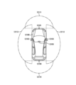
- FIG. 16 is a diagram showing an example of the installation position of the imaging section 12031.
- the imaging unit 12031 includes imaging units 12101, 12102, 12103, 12104, and 12105.
- the imaging units 12101, 12102, 12103, 12104, and 12105 are provided, for example, at positions such as the front nose, side mirrors, rear bumper, back door, and the top of the windshield inside the vehicle 12100.
- An imaging unit 12101 provided in the front nose and an imaging unit 12105 provided above the windshield inside the vehicle mainly acquire images in front of the vehicle 12100.
- Imaging units 12102 and 12103 provided in the side mirrors mainly capture images of the sides of the vehicle 12100.
- An imaging unit 12104 provided in the rear bumper or back door mainly captures images of the rear of the vehicle 12100.
- the imaging unit 12105 provided above the windshield inside the vehicle is mainly used to detect preceding vehicles, pedestrians, obstacles, traffic lights, traffic signs, lanes, and the like.
- FIG. 16 shows an example of the imaging range of the imaging units 12101 to 12104.
- An imaging range 12111 indicates the imaging range of the imaging unit 12101 provided on the front nose
- imaging ranges 12112 and 12113 indicate imaging ranges of the imaging units 12102 and 12103 provided on the side mirrors, respectively
- an imaging range 12114 shows the imaging range of the imaging unit 12101 provided on the front nose.
- the imaging range of the imaging unit 12104 provided in the rear bumper or back door is shown. For example, by overlapping the image data captured by the imaging units 12101 to 12104, an overhead image of the vehicle 12100 viewed from above can be obtained.
- At least one of the imaging units 12101 to 12104 may have a function of acquiring distance information.
- at least one of the imaging units 12101 to 12104 may be a stereo camera including a plurality of image sensors, or may be an image sensor having pixels for phase difference detection.
- the microcomputer 12051 determines the distance to each three-dimensional object within the imaging ranges 12111 to 12114 and the temporal change in this distance (relative speed with respect to the vehicle 12100) based on the distance information obtained from the imaging units 12101 to 12104. In particular, by determining the three-dimensional object that is closest to the vehicle 12100 on its path and that is traveling at a predetermined speed (for example, 0 km/h or more) in approximately the same direction as the vehicle 12100, it is possible to extract the three-dimensional object as the preceding vehicle. can.
- a predetermined speed for example, 0 km/h or more
- the microcomputer 12051 can set an inter-vehicle distance to be secured in advance in front of the preceding vehicle, and perform automatic brake control (including follow-up stop control), automatic acceleration control (including follow-up start control), and the like. In this way, it is possible to perform cooperative control for the purpose of autonomous driving, etc., in which the vehicle travels autonomously without depending on the driver's operation.
- the microcomputer 12051 transfers three-dimensional object data to other three-dimensional objects such as two-wheeled vehicles, regular vehicles, large vehicles, pedestrians, and utility poles based on the distance information obtained from the imaging units 12101 to 12104. It can be classified and extracted and used for automatic obstacle avoidance. For example, the microcomputer 12051 identifies obstacles around the vehicle 12100 into obstacles that are visible to the driver of the vehicle 12100 and obstacles that are difficult to see. Then, the microcomputer 12051 determines a collision risk indicating the degree of risk of collision with each obstacle, and when the collision risk exceeds a set value and there is a possibility of a collision, the microcomputer 12051 transmits information via the audio speaker 12061 and the display unit 12062. By outputting a warning to the driver via the vehicle control unit 12010 and performing forced deceleration and avoidance steering via the drive system control unit 12010, driving support for collision avoidance can be provided.
- the microcomputer 12051 determines a collision risk indicating the degree of risk of collision with each obstacle, and when the collision risk exceed
- At least one of the imaging units 12101 to 12104 may be an infrared camera that detects infrared rays.
- the microcomputer 12051 can recognize a pedestrian by determining whether the pedestrian is present in the images captured by the imaging units 12101 to 12104.
- pedestrian recognition involves, for example, a procedure for extracting feature points in images captured by the imaging units 12101 to 12104 as infrared cameras, and a pattern matching process is performed on a series of feature points indicating the outline of an object to determine whether it is a pedestrian or not.
- the audio image output unit 12052 creates a rectangular outline for emphasis on the recognized pedestrian.
- the display unit 12062 is controlled to display the .
- the audio image output unit 12052 may control the display unit 12062 to display an icon or the like indicating a pedestrian at a desired position.
- the technology according to the present disclosure can be applied to the imaging unit 12031 among the configurations described above.
- the drive circuit of any one of the first to fourth embodiments described above can be applied to the imaging section 12031.
- a pixel array section in which pixels are arranged in a matrix in the row direction and column direction; a current generation section that generates a current;
- a solid-state imaging device comprising: a current driving section that is driven by a shunt current obtained by branching the current generated by the current generating section and generates a drive signal for the pixel based on a control signal.
- the solid-state imaging device according to (1) wherein the current generation section controls the current based on the control signal.
- the control signal includes designation information that designates a current driver to be selected when driving the pixel.
- the solid-state imaging device wherein the designation information is an address assigned to each current drive unit.
- the control signal includes the addresses corresponding to the number of the current drive sections that are simultaneously driven, and a signal that is toggled according to the number of the current drive sections that are simultaneously driven.
- the solid-state imaging device (6) The solid-state imaging device according to (5), wherein the current generation section controls the current based on the number of simultaneously driven current drive sections extracted from the control signal.
- the current generating section controls the current based on a counter output of a signal toggled according to the number of the current driving sections driven simultaneously.
- the current driver includes a first switching element having one end connected to the output terminal,
- the voltage driver includes a second switching element having one end connected to the output terminal,
- the first switching element has the other end connected to a current terminal of the current generation section,
- a plurality of the current drive units are provided, The driver circuit according to any one of (1) to (10), wherein the current generating section is shared by the plurality of current driving sections.
- the solid-state imaging device according to (9) or (10), wherein the voltage drive section is provided corresponding to the current drive section, and the second power supply voltage is supplied in parallel to the voltage drive section. .
- the current driver includes a transistor, A mirror current generated based on a current mirror operation of the current generating section is input to the source of the transistor, The solid-state imaging device according to any one of (1) to (13), wherein the control signal is input to the gate of the transistor.
- a driver circuit comprising: a current driving section that is driven by a shunt current obtained by dividing the current generated by the current generating section and generates a drive signal for a transistor based on a control signal.
- Pixel array section 111 Pixel 102 Vertical drive circuit 103 Horizontal drive circuit 104 Control circuit 105 Column signal processing circuit 106 Output circuit 200 Current source 201-203 Driver 141-143 Voltage protection circuit 151-153, 161-163, 171-173, 181-183 Switching element 130 Power supply 131 Boost circuit 132 Step-down circuit 401-404 AND circuit 405-408 Inverter
Landscapes
- Engineering & Computer Science (AREA)
- Multimedia (AREA)
- Signal Processing (AREA)
- Semiconductor Integrated Circuits (AREA)
- Transforming Light Signals Into Electric Signals (AREA)
- Electronic Switches (AREA)
Abstract
Description
1.第1の実施の形態(電流源で生成された電流に基づいて複数のドライバが駆動される例)
2.第2の実施の形態(同時に駆動されるドライバの個数に応じて電流源で生成される電流を制御する例)
3.第3の実施の形態(電流源の電流制御に基づいてドライバから出力される駆動信号のスルーレートを変化させる例)
4.第4の実施の形態(電流源をドライバ間に分散して配置した例)
5.移動体への応用例
図1は、第1の実施の形態に係る固体撮像装置の構成例を示すブロック図である。
dV+Vgs-Vgs-VRL=dV-VRL<3.0V
となるように可変抵抗320をトリミングする。これにより、ドライバ201のトランジスタの耐圧に整合させた設計が可能となる。
上述の第1の実施の形態では、電流源200で生成された電流IP0およびIN0に基づいて複数のドライバ201乃至203を駆動した。この第2の実施の形態では、ドライバ部を制御する制御信号から同時に駆動されるドライバの個数を抽出し、同時に駆動されるドライバの個数に応じて電流源で生成される電流を制御する。
上述の第2の実施の形態では、駆動信号OUT1乃至OUT3のスルーレートを一定に維持するために、同時に駆動されるドライバ201乃至203の個数Kに応じて可変電流源700で生成される電流IPKおよびINKを制御した。この第3の実施の形態では、可変電流源の電流制御に基づいてドライバ201乃至203から出力される駆動信号OUT1乃至OUT3のスルーレートを変化させる。
上述の第1の実施の形態では、1つの電流源200で生成された電流IP0およびIN0に基づいて複数のドライバ201乃至203を駆動した。この第4の実施の形態では、複数のドライバで共用される電流源を分散配置する。
本開示に係る技術(本技術)は、様々な製品へ応用することができる。例えば、本開示に係る技術は、自動車、電気自動車、ハイブリッド電気自動車、自動二輪車、自転車、パーソナルモビリティ、飛行機、ドローン、船舶、ロボット等のいずれかの種類の移動体に搭載される装置として実現されてもよい。
(1)ロウ方向およびカラム方向にマトリックス状に画素が配置された画素アレイ部と、
電流を生成する電流生成部と、
前記電流生成部で生成された電流が分流された分流電流で駆動され、制御信号に基づいて前記画素の駆動信号を生成する電流駆動部と
を具備する固体撮像装置。
(2)前記電流生成部は、前記制御信号に基づいて前記電流を制御する
前記(1)記載の固体撮像装置。
(3)前記制御信号は、前記画素の駆動時に選択される電流駆動部を指定する指定情報を含む
前記(2)記載の固体撮像装置。
(4)前記指定情報は、前記電流駆動部ごとに割り当てられたアドレスである
前記(3)記載の固体撮像装置。
(5)前記制御信号は、同時に駆動される前記電流駆動部の個数分の前記アドレスと、同時に駆動される前記電流駆動部の個数に応じてトグルされる信号とを含む
前記(4)記載の固体撮像装置。
(6)前記電流生成部は、前記制御信号から抽出された同時に駆動される前記電流駆動部の個数に基づいて前記電流を制御する
前記(5)記載の固体撮像装置。
(7)前記電流生成部は、同時に駆動される前記電流駆動部の個数に応じてトグルされる信号のカウンタ出力に基づいて、前記電流を制御する
前記(6)記載の固体撮像装置。
(8)前記カウンタ出力に応じた個数分の前記アドレスでそれぞれ特定される前記電流駆動部は、前記カウンタ出力にて制御された電流に基づいて同時に電流駆動される
前記(7)記載の固体撮像装置。
(9)前記電流生成部に供給される第1電源電圧と異なる第2電源電圧が供給され、前記制御信号に基づいて前記画素の駆動信号を生成する電圧駆動部と、
前記電流駆動部と前記電圧駆動部とで共通に設けられた出力端子と
をさらに具備する前記(1)から(8)のいずれかに記載の固体撮像装置。
(10)前記電流駆動部は、前記出力端子に一端が接続される第1スイッチング素子を備え、
前記電圧駆動部は、前記出力端子に一端が接続される第2スイッチング素子を備え、
前記第1スイッチング素子は、前記電流生成部の電流端子に他端が接続され、
前記第2スイッチング素子は、前記第2電源電圧が他端に供給される
前記(9)記載の固体撮像装置。
(11)前記電流駆動部は複数設けられ、
前記電流生成部は、前記複数の電流駆動部で共有される
前記(1)から(10)のいずれかに記載のドライバ回路。
(12)前記電流駆動部は、前記電流生成部に並列に接続される
前記(11)記載のドライバ回路。
(13)前記電圧駆動部は前記電流駆動部にそれぞれ対応して設けられ、前記第2電源電圧は前記電圧駆動部に並列に供給される
前記(9)または(10)に記載の固体撮像装置。
(14)前記電流駆動部はトランジスタを備え、
前記電流生成部のカレントミラー動作に基づいて生成されたミラー電流が前記トランジスタのソースに入力され、
前記制御信号は前記トランジスタのゲートに入力される
前記(1)から(13)のいずれかに記載の固体撮像装置。
(15)前記電流生成部のカレントミラー動作に基づいて生成されるミラー電流の制御に基づいて、前記電流駆動部のスルーレートを制御するスルーレート制御部をさらに具備する前記(14)記載の固体撮像装置。
(16)電流を生成する電流生成部と、
前記電流生成部で生成された電流が分流された分流電流で駆動され、制御信号に基づいてトランジスタの駆動信号を生成する電流駆動部と
を具備するドライバ回路。
111 画素
102 垂直駆動回路
103 水平駆動回路
104 制御回路
105 カラム信号処理回路
106 出力回路
200 電流源
201~203 ドライバ
141~143 耐圧保護回路
151~153、161~163、171~173、181~183 スイッチング素子
130 電源
131 昇圧回路
132 降圧回路
401~404 論理積回路
405~408 インバータ
Claims (16)
- ロウ方向およびカラム方向にマトリックス状に画素が配置された画素アレイ部と、
電流を生成する電流生成部と、
前記電流生成部で生成された電流が分流された分流電流で駆動され、制御信号に基づいて前記画素の駆動信号を生成する電流駆動部と
を具備する固体撮像装置。 - 前記電流生成部は、前記制御信号に基づいて前記電流を制御する
請求項1記載の固体撮像装置。 - 前記制御信号は、前記画素の駆動時に選択される電流駆動部を指定する指定情報を含む
請求項2記載の固体撮像装置。 - 前記指定情報は、前記電流駆動部ごとに割り当てられたアドレスである
請求項3記載の固体撮像装置。 - 前記制御信号は、同時に駆動される前記電流駆動部の個数分の前記アドレスと、同時に駆動される前記電流駆動部の個数に応じてトグルされる信号とを含む
請求項4記載の固体撮像装置。 - 前記電流生成部は、前記制御信号から抽出された同時に駆動される前記電流駆動部の個数に基づいて前記電流を制御する
請求項5記載の固体撮像装置。 - 前記電流生成部は、同時に駆動される前記電流駆動部の個数に応じてトグルされる信号のカウンタ出力に基づいて、前記電流を制御する
請求項6記載の固体撮像装置。 - 前記カウンタ出力に応じた個数分の前記アドレスでそれぞれ特定される前記電流駆動部は、前記カウンタ出力にて制御された電流に基づいて同時に電流駆動される
請求項7記載の固体撮像装置 - 前記電流生成部に供給される第1電源電圧と異なる第2電源電圧が供給され、前記制御信号に基づいて前記画素の駆動信号を生成する電圧駆動部と、
前記電流駆動部と前記電圧駆動部とで共通に設けられた出力端子と
をさらに具備する請求項1記載の固体撮像装置。 - 前記電流駆動部は、前記出力端子に一端が接続される第1スイッチング素子を備え、
前記電圧駆動部は、前記出力端子に一端が接続される第2スイッチング素子を備え、
前記第1スイッチング素子は、前記電流生成部の電流端子に他端が接続され、
前記第2スイッチング素子は、前記第2電源電圧が他端に供給される
請求項9記載の固体撮像装置。 - 前記電流駆動部は複数設けられ、
前記電流生成部は、前記複数の電流駆動部で共有される
請求項1記載のドライバ回路。 - 前記電流駆動部は、前記電流生成部に並列に接続される
請求項8記載のドライバ回路。 - 前記電圧駆動部は前記電流駆動部にそれぞれ対応して設けられ、前記第2電源電圧は前記電圧駆動部に並列に供給される
請求項9記載の固体撮像装置。 - 前記電流駆動部はトランジスタを備え、
前記電流生成部のカレントミラー動作に基づいて生成されたミラー電流が前記トランジスタのソースに流れ、
前記制御信号は前記トランジスタのゲートに入力される
請求項1記載の固体撮像装置。 - 前記電流生成部のカレントミラー動作に基づいて生成されるミラー電流の制御に基づいて、前記電流駆動部のスルーレートを制御するスルーレート制御部をさらに具備する請求項14記載の固体撮像装置。
- 電流を生成する電流生成部と、
前記電流生成部で生成された電流が分流された分流電流で駆動され、制御信号に基づいてトランジスタの駆動信号を生成する電流駆動部と
を具備するドライバ回路。
Priority Applications (1)
| Application Number | Priority Date | Filing Date | Title |
|---|---|---|---|
| US18/865,837 US20250324172A1 (en) | 2022-05-24 | 2023-03-27 | Solid-state imaging device and driver circuit |
Applications Claiming Priority (2)
| Application Number | Priority Date | Filing Date | Title |
|---|---|---|---|
| JP2022-084200 | 2022-05-24 | ||
| JP2022084200A JP2023172419A (ja) | 2022-05-24 | 2022-05-24 | 固体撮像装置およびドライバ回路 |
Publications (1)
| Publication Number | Publication Date |
|---|---|
| WO2023228545A1 true WO2023228545A1 (ja) | 2023-11-30 |
Family
ID=88919042
Family Applications (1)
| Application Number | Title | Priority Date | Filing Date |
|---|---|---|---|
| PCT/JP2023/012142 Ceased WO2023228545A1 (ja) | 2022-05-24 | 2023-03-27 | 固体撮像装置およびドライバ回路 |
Country Status (3)
| Country | Link |
|---|---|
| US (1) | US20250324172A1 (ja) |
| JP (1) | JP2023172419A (ja) |
| WO (1) | WO2023228545A1 (ja) |
Citations (3)
| Publication number | Priority date | Publication date | Assignee | Title |
|---|---|---|---|---|
| JP2009290703A (ja) * | 2008-05-30 | 2009-12-10 | Panasonic Corp | 固体撮像装置およびカメラ |
| JP2016019175A (ja) * | 2014-07-09 | 2016-02-01 | ルネサスエレクトロニクス株式会社 | 固体撮像装置、画像データ伝送方法、およびカメラシステム |
| WO2021161658A1 (ja) * | 2020-02-12 | 2021-08-19 | ソニーセミコンダクタソリューションズ株式会社 | ドライバ回路および撮像装置 |
-
2022
- 2022-05-24 JP JP2022084200A patent/JP2023172419A/ja active Pending
-
2023
- 2023-03-27 WO PCT/JP2023/012142 patent/WO2023228545A1/ja not_active Ceased
- 2023-03-27 US US18/865,837 patent/US20250324172A1/en active Pending
Patent Citations (3)
| Publication number | Priority date | Publication date | Assignee | Title |
|---|---|---|---|---|
| JP2009290703A (ja) * | 2008-05-30 | 2009-12-10 | Panasonic Corp | 固体撮像装置およびカメラ |
| JP2016019175A (ja) * | 2014-07-09 | 2016-02-01 | ルネサスエレクトロニクス株式会社 | 固体撮像装置、画像データ伝送方法、およびカメラシステム |
| WO2021161658A1 (ja) * | 2020-02-12 | 2021-08-19 | ソニーセミコンダクタソリューションズ株式会社 | ドライバ回路および撮像装置 |
Also Published As
| Publication number | Publication date |
|---|---|
| JP2023172419A (ja) | 2023-12-06 |
| US20250324172A1 (en) | 2025-10-16 |
Similar Documents
| Publication | Publication Date | Title |
|---|---|---|
| JP2020136958A (ja) | イベント信号検出センサ及び制御方法 | |
| WO2022038885A1 (ja) | 固体撮像素子、および、撮像装置 | |
| WO2020066245A1 (ja) | 固体撮像素子、および、撮像装置 | |
| CN111066248B (zh) | 电压转换电路、固体摄像元件及电压转换电路的控制方法 | |
| WO2022038895A1 (ja) | 固体撮像素子、および、撮像装置 | |
| US12058458B2 (en) | Imaging device and imaging system | |
| WO2021010036A1 (ja) | 固体撮像素子、撮像装置および固体撮像素子の制御方法 | |
| JP7741810B2 (ja) | 固体撮像装置 | |
| WO2023228545A1 (ja) | 固体撮像装置およびドライバ回路 | |
| WO2021192460A1 (ja) | センシングデバイス、および、電子装置 | |
| US12294800B2 (en) | Solid-state imaging element | |
| WO2023153104A1 (ja) | 信号生成回路および光検出装置 | |
| WO2021181856A1 (ja) | 固体撮像素子、撮像装置、および、固体撮像素子の制御方法 | |
| WO2022244321A1 (ja) | 光検出装置、光検出システム、および光検出方法 | |
| JP2023072096A (ja) | チャージポンプ回路および昇圧方法 | |
| US12452561B2 (en) | Image capturing apparatus and electronic device | |
| JP2020141362A (ja) | 光検出装置 | |
| WO2023248633A1 (ja) | 撮像装置およびチャージポンプ回路 | |
| WO2022137993A1 (ja) | コンパレータ及び固体撮像素子 | |
| WO2022209368A1 (ja) | 固体撮像素子及び固体撮像装置 | |
| WO2023058345A1 (ja) | 撮像装置 | |
| WO2023223742A1 (ja) | 光検出素子、タイミング発生器及びad変換器 | |
| WO2021124628A1 (ja) | 固体撮像素子、および、撮像装置 | |
| US20230049629A1 (en) | Solid-state imaging element and imaging device | |
| WO2023074522A1 (ja) | 物理量検出装置及び撮像装置 |
Legal Events
| Date | Code | Title | Description |
|---|---|---|---|
| 121 | Ep: the epo has been informed by wipo that ep was designated in this application |
Ref document number: 23811424 Country of ref document: EP Kind code of ref document: A1 |
|
| WWE | Wipo information: entry into national phase |
Ref document number: 18865837 Country of ref document: US |
|
| NENP | Non-entry into the national phase |
Ref country code: DE |
|
| 122 | Ep: pct application non-entry in european phase |
Ref document number: 23811424 Country of ref document: EP Kind code of ref document: A1 |
|
| WWP | Wipo information: published in national office |
Ref document number: 18865837 Country of ref document: US |