WO2023228496A1 - Dispositif à semi-conducteur d'alimentation électrique et convertisseur d'amplification - Google Patents
Dispositif à semi-conducteur d'alimentation électrique et convertisseur d'amplification Download PDFInfo
- Publication number
- WO2023228496A1 WO2023228496A1 PCT/JP2023/006174 JP2023006174W WO2023228496A1 WO 2023228496 A1 WO2023228496 A1 WO 2023228496A1 JP 2023006174 W JP2023006174 W JP 2023006174W WO 2023228496 A1 WO2023228496 A1 WO 2023228496A1
- Authority
- WO
- WIPO (PCT)
- Prior art keywords
- voltage
- terminal
- feedback
- output terminal
- comparison
- Prior art date
Links
- 239000004065 semiconductor Substances 0.000 title claims abstract description 40
- 238000012544 monitoring process Methods 0.000 claims abstract description 8
- 230000005540 biological transmission Effects 0.000 claims description 10
- 239000003990 capacitor Substances 0.000 claims description 9
- 241001125929 Trisopterus luscus Species 0.000 description 81
- 230000001360 synchronised effect Effects 0.000 description 26
- 238000010586 diagram Methods 0.000 description 9
- 230000007704 transition Effects 0.000 description 7
- 230000005856 abnormality Effects 0.000 description 6
- 230000005669 field effect Effects 0.000 description 4
- 238000000034 method Methods 0.000 description 4
- 230000007423 decrease Effects 0.000 description 3
- 238000010977 unit operation Methods 0.000 description 3
- 238000009413 insulation Methods 0.000 description 2
- 238000012986 modification Methods 0.000 description 2
- 230000004048 modification Effects 0.000 description 2
- 239000004020 conductor Substances 0.000 description 1
- 238000012217 deletion Methods 0.000 description 1
- 230000037430 deletion Effects 0.000 description 1
- 239000002184 metal Substances 0.000 description 1
- 239000011347 resin Substances 0.000 description 1
- 229920005989 resin Polymers 0.000 description 1
- 230000000087 stabilizing effect Effects 0.000 description 1
- 238000006467 substitution reaction Methods 0.000 description 1
- 239000000758 substrate Substances 0.000 description 1
Images


Classifications
-
- H—ELECTRICITY
- H02—GENERATION; CONVERSION OR DISTRIBUTION OF ELECTRIC POWER
- H02M—APPARATUS FOR CONVERSION BETWEEN AC AND AC, BETWEEN AC AND DC, OR BETWEEN DC AND DC, AND FOR USE WITH MAINS OR SIMILAR POWER SUPPLY SYSTEMS; CONVERSION OF DC OR AC INPUT POWER INTO SURGE OUTPUT POWER; CONTROL OR REGULATION THEREOF
- H02M3/00—Conversion of dc power input into dc power output
- H02M3/02—Conversion of dc power input into dc power output without intermediate conversion into ac
- H02M3/04—Conversion of dc power input into dc power output without intermediate conversion into ac by static converters
- H02M3/10—Conversion of dc power input into dc power output without intermediate conversion into ac by static converters using discharge tubes with control electrode or semiconductor devices with control electrode
- H02M3/145—Conversion of dc power input into dc power output without intermediate conversion into ac by static converters using discharge tubes with control electrode or semiconductor devices with control electrode using devices of a triode or transistor type requiring continuous application of a control signal
- H02M3/155—Conversion of dc power input into dc power output without intermediate conversion into ac by static converters using discharge tubes with control electrode or semiconductor devices with control electrode using devices of a triode or transistor type requiring continuous application of a control signal using semiconductor devices only
Definitions
- the present disclosure relates to a power supply semiconductor device and a boost converter.
- a boost converter that boosts the input voltage monitors the boosted voltage and is provided with a feedback terminal that receives feedback of the boosted voltage. By performing switching control based on the feedback voltage applied to the feedback terminal, the boosted voltage can be stabilized at a desired target voltage.
- the boost converter may mistakenly recognize that the boost is insufficient. , there is a risk of excessive pressure increase. Excessive voltage boosting may damage components that receive the boosted voltage.
- An object of the present disclosure is to provide a power supply semiconductor device and a boost converter that contribute to suppressing excessive boosting in the event of a failure.
- a power supply semiconductor device is a power supply semiconductor device used in a boost converter that boosts an input voltage.
- a switching circuit configured to generate a boosted output terminal voltage at the output terminal; a feedback terminal to receive a monitored voltage corresponding to the output terminal voltage through external wiring of the power supply semiconductor device;
- a control drive circuit configured to control the switching circuit based on an error between a predetermined reference voltage and a comparison voltage based on the feedback voltage applied to the terminal and the output terminal voltage.
- FIG. 1 is an overall configuration diagram of a boost converter according to an embodiment of the present disclosure.
- FIG. 2 is an external perspective view of a power supply IC according to an embodiment of the present disclosure.
- FIG. 3 is a diagram illustrating a state in which a break occurs in the feedback wiring (open failure state) in the boost converter according to the embodiment of the present disclosure.
- FIG. 4 is an overall configuration diagram of a boost converter according to a first example belonging to an embodiment of the present disclosure.
- FIG. 5 is a diagram showing a boost converter in a normally connected state, according to a first example belonging to an embodiment of the present disclosure.
- FIG. 6 is a diagram illustrating a boost converter in an open failure state according to a first example belonging to an embodiment of the present disclosure.
- FIG. 1 is an overall configuration diagram of a boost converter according to an embodiment of the present disclosure.
- FIG. 2 is an external perspective view of a power supply IC according to an embodiment of the present disclosure.
- FIG. 3 is a diagram illustrating a
- FIG. 7 is an overall configuration diagram of a boost converter according to a second example belonging to an embodiment of the present disclosure.
- FIG. 8 is a diagram showing a boost converter in a normally connected state, according to a second example belonging to the embodiment of the present disclosure.
- FIG. 9 is a diagram showing a boost converter in an open failure state, according to a second example belonging to the embodiment of the present disclosure.
- IC is an abbreviation for integrated circuit.
- the ground refers to a reference conductive portion having a reference potential of 0V (zero volts), or refers to the 0V potential itself.
- the reference conductive part may be formed using a conductor such as metal.
- the potential of 0V is sometimes referred to as a ground potential.
- voltages shown without particular reference represent potentials as seen from ground.
- Level refers to the level of potential, and for any signal or voltage of interest, a high level has a higher potential than a low level.
- a signal or voltage being at a high level strictly means that the level of the signal or voltage is at a high level, and a signal or voltage being at a low level does not strictly mean that the level of the signal or voltage is at a high level. It means that the signal or voltage level is at low level.
- the level of a signal may be expressed as a signal level, and the level of a voltage may be expressed as a voltage level.
- an on state refers to a state in which the drain and source of the transistor are electrically connected
- an off state refers to a state in which the drain and source of the transistor are electrically connected. Refers to the state where there is no conduction between the two (blocked state).
- the MOSFET is understood to be an enhancement type MOSFET unless otherwise specified.
- MOSFET is an abbreviation for "metal-oxide-semiconductor field-effect transistor.”
- the back gate of any MOSFET may be considered to be short-circuited to the source.
- MOSFET The electrical characteristics of MOSFET include gate threshold voltage.
- the gate potential of the transistor is higher than the source potential of the transistor, and the gate-source voltage (gate potential seen from the source potential) of the transistor is When the magnitude is greater than or equal to the gate threshold voltage of the transistor, the transistor is in the on state; otherwise, the transistor is in the off state.
- the gate potential of the transistor is lower than the source potential of the transistor, and the gate-source voltage (gate potential seen from the source potential) of the transistor is lower than the gate potential of the transistor.
- the gate threshold voltage is the gate threshold voltage required to cause a predetermined amount of drain current to flow when a predetermined voltage is applied between the drain and source of the FET under a predetermined ambient temperature environment. — defined as the source-to-source voltage.
- Any switch element can be composed of one or more FETs (field effect transistors), and when a switch element is in an on state, conduction occurs between both ends of the switch element, while a certain switch element is in an off state. Sometimes, there is no conduction between both ends of the switch element.
- FETs field effect transistors
- the on state and off state of any transistor or switch element may be simply expressed as on or off.
- switching from an off state to an on state is expressed as turn-on, and switching from an on state to an off state is expressed as turn-off.
- the period in which the transistor or switch element is in the on state may be referred to as the on period, and the period in which the transistor or switch element is in the off state may be referred to as the off period. be.
- Connections between multiple parts forming a circuit such as arbitrary circuit elements, wiring (lines), and nodes, may be understood to refer to electrical connections, unless otherwise specified.
- FIG. 1 is an overall configuration diagram of a boost converter 1 according to an embodiment of the present disclosure.
- the boost converter 1 in FIG. 1 includes a power supply IC 2 which is a power supply semiconductor device, and a plurality of discrete components externally connected to the power supply IC 2.
- the plurality of discrete components provided in boost converter 1 include inductor L0 and output capacitor C0.
- the step-up converter 1 is a step-up switching power supply device (DC/DC converter) that receives an input voltage V IN supplied from the outside and generates a voltage that is a step-up of the input voltage V IN .
- DC/DC converter step-up switching power supply device
- FIG. 2 shows an external perspective view of the power supply IC 2.
- the power supply IC 2 includes a semiconductor chip having a semiconductor integrated circuit formed on a semiconductor substrate, a casing (package) that houses the semiconductor chip, and a plurality of external terminals exposed to the outside of the power supply IC 2 from the casing. It is an electronic component equipped with The power supply IC 2 is formed by enclosing a semiconductor chip in a housing (package) made of resin. Note that the number of external terminals of the power supply IC 2 and the type of casing of the power supply IC 2 shown in FIG. 2 are merely examples, and they can be designed arbitrarily.
- FIG. 1 only the input terminal IN, output terminal POUT, switch terminal SW, ground terminal PGND, and feedback terminal FB are shown as some of the plurality of external terminals provided in the power supply IC 2, but other external terminals (for example, an enable terminal or a power good terminal) is also provided in the power supply IC2.
- the wiring provided in the boost converter 1 the wiring provided outside the power supply IC2 is particularly referred to as an external wiring, and the wiring provided inside the power supply IC2 is particularly referred to as an internal wiring.
- An input voltage V IN is supplied to the input terminal IN from a voltage source (not shown).
- the input voltage V IN is a positive DC voltage.
- One end of the inductor L0 is connected to a terminal to which the input voltage V IN is applied and receives the input voltage V IN . It may be understood that one end of the inductor L0 is connected to the input terminal IN. The other end of inductor L0 is connected to switching terminal SW.
- a ground terminal PGND is connected to ground.
- Boost converter 1 is provided with output wiring WR1 as an external wiring connected to output terminal POUT.
- One end of the output wiring WR1 is connected to the output terminal POUT, and the other end of the output wiring WR1 is connected to the load LD.
- the voltage applied to the output terminal POUT is referred to as the output terminal voltage V POUT .
- a voltage corresponding to the output terminal voltage V POUT is supplied to the load LD as the load voltage V LD .
- the load LD is one or more arbitrary loads that are driven based on the load voltage VLD .
- the current supplied to the load LD through the output wiring WR1 is referred to as a load current ILD .
- the load current I LD flows from the output terminal POUT toward the load LD.
- One end of the output capacitor C0 is connected to the output wiring WR1, and the other end of the output capacitor C0 is connected to ground.
- a feedback wiring WR2 is provided in boost converter 1 as an external wiring connected to feedback terminal FB.
- One end of the feedback wiring WR2 is connected to the feedback terminal FB, and the other end of the feedback wiring WR2 is connected to the node ND0.
- the node ND0 is a node on the output wiring WR1, and is provided at a position as close as possible to the load LD on the output wiring WR1. At least the distance between node ND0 and load LD is shorter than the distance between node ND0 and output terminal POUT.
- the load voltage V LD is the voltage at the node ND0.
- the load voltage VLD corresponds to a target voltage (monitored voltage) to be monitored in the power supply IC2.
- the voltage applied to the feedback terminal FB is referred to as a feedback voltage V FB .
- the output terminal voltage V POUT is a boosted voltage generated by boosting the input voltage V IN and is therefore higher than the input voltage V IN .
- the load voltage V LD is also a boosted voltage generated by boosting the input voltage V IN and is therefore higher than the input voltage V IN .
- the load current I LD is zero, the value of the load voltage V LD is equal to the value of the output terminal voltage V POUT .
- the load current I LD is not zero, a voltage drop corresponding to the wiring resistance in the output wiring WR1 and the load current I LD occurs between the output terminal POUT and the node ND0, so the load voltage V LD increases by the voltage drop. becomes lower than the output terminal voltage V POUT .
- a switching circuit 10 and a control drive circuit 20 are provided in the power supply IC 2.
- the switching circuit 10 includes a switching transistor 11 and a rectifying element 12.
- a synchronous rectification transistor is used as the rectification element 12.
- the switching transistor 11 is configured with an N-channel type MOSFET
- the synchronous rectification transistor 12 is configured with a P-channel type MOSFET.
- the source of the synchronous rectifier transistor 12 is connected to the output terminal POUT.
- the drain of the synchronous rectifier transistor 12 and the drain of the switching transistor 11 are commonly connected to the switch terminal SW.
- the source of the switching transistor 11 is connected to the ground terminal PGND (therefore, connected to the ground via the ground terminal PGND).
- the power supply IC2 is provided with an internal wiring WR11 connected to the output terminal POUT and an internal wiring WR12 connected to the feedback terminal FB.
- Output terminal voltage V POUT is applied to internal wiring WR11
- feedback voltage V FB is applied to internal wiring WR12.
- the control drive circuit 20 is driven based on the internal power supply voltage.
- An internal power supply circuit (not shown) provided in the power supply IC 2 generates an internal power supply voltage from the input voltage V IN .
- the control drive circuit 20 is connected to an output terminal POUT via an internal wiring WR11 and to a feedback terminal FB via an internal wiring WR12. Therefore, the feedback voltage V FB at the feedback terminal FB and the output terminal voltage V POUT at the output terminal POUT are input to the control drive circuit 20.
- a predetermined reference voltage V REF is input to the control drive circuit 20 .
- a reference voltage generation circuit (not shown) provided in the power supply IC 2 generates a reference voltage V REF based on the input voltage V IN .
- the reference voltage V REF has a predetermined positive DC voltage value.
- the control drive circuit 20 basically generates a comparison voltage based on the feedback voltage VFB .
- the control drive circuit 20 then performs switching control on the switching circuit 10 so that the error between the comparison voltage and the reference voltage V REF is reduced (so that the error converges to zero).
- the comparison voltage generated based on the feedback voltage V FB is a divided voltage of the feedback voltage V FB . Therefore, when the comparison voltage is generated based on the feedback voltage V FB , the target voltage V TG (not shown) determined by the voltage division ratio and the reference voltage V REF when generating the comparison voltage from the feedback voltage V FB is As a result, the load voltage V LD is stabilized.
- the control drive circuit 20 is connected to each gate of the switching transistor 11 and the synchronous rectification transistor 12, and controls the states of the switching transistor 11 and the synchronous rectification transistor 12 by controlling each gate potential of the switching transistor 11 and the synchronous rectification transistor 12. do.
- the control drive circuit 20 alternately turns on and off the switching transistor 11 and the synchronous rectification transistor 12 in the switching control described above. During the ON period of the switching transistor 11, the synchronous rectification transistor 12 is controlled to be OFF, and during the ON period of the synchronous rectification transistor 12, the switching transistor 11 is controlled to be OFF.
- a current flows from the terminal to which the input voltage V IN is applied to the ground through the inductor L0, the switch terminal SW, and the channel of the switching transistor 11, so that energy is accumulated in the inductor L0.
- a current based on the stored energy of the inductor L0 flows from the terminal to which the input voltage V IN is applied, to the inductor L0, to the switch terminal SW, to the synchronous rectification transistor. It is supplied to the output capacitor C0 and the load LD through the 12 channels and the output terminal POUT.
- the control drive circuit 20 may perform switching control using PWM.
- PWM is an abbreviation for Pulse Width Modulation.
- the switching transistor 11 and the synchronous rectifier transistor 12 are alternately turned on and off at a predetermined PWM frequency, and the on-duty of the switching transistor 11 is adjusted based on the comparison voltage and the reference voltage V REF .
- the on-duty of the switching transistor 11 refers to the ratio of the length of the on-period of the switching transistor 11 that occupies one PWM period in each PWM period.
- the control drive circuit 20 may perform switching control using PFM.
- PFM is an abbreviation for Pulse Frequency Modulation.
- the switching transistor 11 and the synchronous rectifier transistor 12 are alternately turned on and off at a variable switching frequency, and the switching frequency is adjusted based on the comparison voltage and the reference voltage V REF .
- the ON time (length of ON period) of the switching transistor 11 per time is constant. That is, in switching control using PFM, after turning on the switching transistor 11 and turning off the synchronous rectifier transistor 12 for a certain period of time, a unit operation is repeated in which the switching transistor 11 is turned off and the synchronous rectifier transistor 12 is kept on, and the unit operation is repeated.
- the repetition frequency of unit operation i.e., switching frequency of switching control by PFM
- the amount of energy transmitted from the terminal to which input voltage V IN is applied to output capacitor C0 and load LD increases, and as a result, the output terminal voltage V POUT and the load voltage V LD rise.
- the normal connection state is a state in which the load voltage V LD (ie, the voltage to be monitored), which is a voltage corresponding to the output terminal voltage VP OUT , is applied to the feedback terminal FB through the feedback wiring WR2.
- FIG. 1 shows a boost converter 1 in a normally connected state. In a normal connection state, the current flowing through the feedback wiring WR2 is minute, and the feedback voltage V FB can be considered to match the load voltage V LD .
- an abnormality in the feedback wiring WR2 is a disconnection of the feedback wiring WR2.
- An abnormality in which the feedback terminal FB becomes open due to an abnormality in the feedback wiring WR2 or due to a poor connection between the feedback wiring WR2 and the feedback terminal FB is referred to as an open failure state (see FIG. 3).
- the feedback terminal FB and the node ND0 may be equivalent to a state in which they are connected via a resistance component of, for example, several hundred kilohms. However, here, it is assumed that in the open failure state, the feedback terminal FB and the node ND0 are insulated with a sufficiently high insulation resistance.
- a state in which the transmission of the load voltage V LD (ie, the voltage to be monitored) to the feedback terminal FB is cut off belongs to an open fault state.
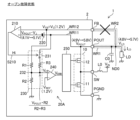
- FIG. 4 shows the configuration of a boost converter 1 according to the first embodiment.
- the boost converter 1 according to the first embodiment includes a control drive circuit 20A as the control drive circuit 20.
- the configuration of the control drive circuit 20A will be explained.
- the control drive circuit 20A includes a comparator 210, a voltage source 220, a comparison voltage generation circuit 230, an error amplifier 240, and a circuit 250 including a logic circuit and a drive circuit.
- Comparator 210 has an inverting input terminal, a non-inverting input terminal, and an output terminal.
- Voltage source 220 generates and outputs a predetermined judgment voltage V J .
- the determination voltage V J has a predetermined positive DC voltage value (for example, 0.8V).
- Voltage source 220 is inserted between the non-inverting input terminal and output terminal POUT of comparator 210, and at this time, the positive output end of voltage source 220 is connected to internal wiring WR11. Therefore, the voltage source 220 supplies the non-inverting input terminal of the comparator 210 with a voltage (V POUT ⁇ V J ) lower than the output terminal voltage V POUT by the determination voltage V J .
- the inverting input terminal of the comparator 210 is connected to the feedback terminal FB via the internal wiring WR12, and receives the voltage applied to the feedback terminal FB (ie, the feedback voltage V FB ).
- the comparator 210 compares a voltage (V POUT ⁇ V J ) lower than the output terminal voltage V POUT by the determination voltage V J with the feedback voltage V FB and outputs a signal S210 indicating the comparison result from its own output terminal.
- the comparator 210 outputs a high level signal S210 when the voltage (V POUT - V J ) is higher than the feedback voltage V FB , and outputs a low level signal S210 when the voltage (V POUT - V J ) is lower than the feedback voltage V FB .
- the comparison voltage generation circuit 230 includes resistors R1 to R3 and a switch element 231, and generates a comparison voltage V C based on the feedback voltage V FB and the output terminal voltage V POUT .
- One end of the resistor R1 is connected to the feedback terminal FB via an internal wiring WR12 to receive the voltage (ie, feedback voltage V FB ) applied to the feedback terminal FB.
- the other end of resistor R1 is connected to node 232.
- One end of resistor R2 is connected to node 232.
- the other end of resistor R2 is connected to ground.
- Resistors R1 and R2 constitute a voltage divider circuit that divides the feedback voltage VFB .
- One end of the switch element 231 is connected to the output terminal POUT via the internal wiring WR11 and receives the output terminal voltage V POUT .
- the other end of switch element 231 is connected to one end of resistor R3, and the other end of resistor R3 is connected to node 232.
- the above-mentioned target voltage V TG is determined by the voltage division ratio by the resistors R1 and R2 and the reference voltage V REF .
- the resistance values of the resistors R1, R2, and R3 are represented by "R1,""R2,” and "R3,” respectively.
- Switch element 231 is controlled to be turned on or off based on output signal S210 of comparator 210.
- the switch element 231 is controlled to be turned off when the signal S210 is at a low level, and controlled to be turned on when the signal S210 is at a high level.
- Error amplifier 240 includes an inverting input terminal, a non-inverting input terminal, and an output terminal.
- a non-inverting input terminal of error amplifier 240 is connected to node 232 and receives comparison voltage V C .
- a reference voltage V REF is supplied to the inverting input terminal of the error amplifier 240 .
- the error amplifier 240 generates an error signal V ERR based on the error between the comparison voltage V C and the reference voltage V REF , and outputs the error signal V ERR from its own output terminal.
- the error amplifier 240 increases the potential of the error signal V ERR when the comparison voltage V C is higher than the reference voltage V REF , and increases the potential of the error signal V ERR when the comparison voltage V C is lower than the reference voltage V REF . lower.
- the circuit 250 performs switching control on the switching circuit 10 based on the error signal V ERR so that the error between the comparison voltage V C and the reference voltage V REF is reduced (so that the error converges to zero).
- the circuit 250 is connected to each gate of the switching transistor 11 and the synchronous rectification transistor 12, and controls the states of the switching transistor 11 and the synchronous rectification transistor 12 by controlling each gate potential of the switching transistor 11 and the synchronous rectification transistor 12.
- the circuit 250 alternately turns on and off the switching transistor 11 and the synchronous rectification transistor 12 in the switching control described above.
- voltage source 210 and boost converter 1 are configured so that “ ⁇ V ⁇ V J ” holds true. Therefore, in a normal connection state, "V POUT -V J ⁇ V FB " is established and the signal S210 becomes low level.
- V TG for the load voltage V LD
- V ⁇ V 0.1V
- V J determination voltage
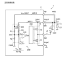
- the output terminal voltage V POUT is 4.9 V and the feedback voltage V FB as shown in FIG.
- V REF the reference voltage V REF is 1.2V. In this case, by setting the resistance value of the resistor R1 to three times the resistance value of the resistor R2, the target voltage V TG with respect to the load voltage V LD becomes 4.8V in a normal connection state.
- the resistance value of the resistor R3 is set larger than the resistance value of the resistor R1. Therefore, the output terminal voltage V POUT and the load voltage V LD in the open fault state are higher than the output terminal voltage V POUT and the load voltage V LD in the normal connection state.
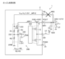
- the values of resistors R2 and R3 and the reference voltage V REF are adjusted so that the output terminal voltage V POUT becomes 5.8V. is set. Therefore, when transitioning from the normal connection state in FIG. 5 to the open failure state in FIG. 6, after the switch element 231 is turned on, the output terminal voltage V V POUT is stabilized at 5.8V, and at this time, the load voltage V LD is stabilized at 5.7V (assuming voltage ⁇ V is fixed at 0.1V).
- the comparison voltage generation circuit 230 generates the feedback voltage V FB according to the level relationship between the feedback voltage V FB and the voltage (V POUT - V J ) that is lower than the output terminal voltage V POUT by a predetermined judgment voltage V J .
- the comparison voltage V C is generated by switching and using either of the output terminal voltage V POUT and the output terminal voltage V POUT.
- a comparison voltage V C is generated based on the feedback voltage V FB .
- the open fault state "V POUT -V J >V FB ", and in this case, the comparison voltage V C is generated based on the output terminal voltage V POUT without depending on the feedback voltage V FB .
- the circuit 250 may perform switching control using PWM.
- switching control using PWM the switching transistor 11 and the synchronous rectifier transistor 12 are alternately turned on and off at a predetermined PWM frequency, and the on-duty of the switching transistor 11 is adjusted based on the error signal VERR .
- the circuit 250 reduces the on-duty of the switching transistor 11 as the error signal V ERR rises in order to reduce the error between the comparison voltage V C and the reference voltage V REF , and reduces the on-duty of the switching transistor 11 as the error signal V ERR increases.
- the on-duty of the switching transistor 11 is increased as the ERR decreases.
- control drive circuit 20 may perform switching control using PFM.
- switching control using PFM the switching transistor 11 and the synchronous rectifier transistor 12 are alternately turned on and off at a variable switching frequency, and the switching frequency is adjusted based on the error signal VERR .
- the ON time (length of ON period) of the switching transistor 11 per time is constant.
- the circuit 250 lowers the switching frequency as the error signal V ERR increases in order to reduce the error between the comparison voltage V C and the reference voltage V REF , and as the error signal V ERR decreases. Accordingly, the switching frequency is increased.
- FIG. 7 shows the configuration of a boost converter 1 according to a second embodiment.
- the boost converter 1 according to the second embodiment includes a control drive circuit 20B as the control drive circuit 20.
- the control drive circuit 20B includes a comparison voltage generation circuit 230B, an error amplifier 240, and a circuit 250 including a logic circuit and a drive circuit.
- the comparator 210 and voltage source 220 shown in FIG. 4 are unnecessary. That is, by deleting the comparator 210 and the voltage source 220 and replacing the comparison voltage generation circuit 230 of FIG. 4 with the comparison voltage generation circuit 230B based on the control drive circuit 20A of FIG. 20B is obtained. Except for the above deletions and substitutions, the control drive circuit 20B has the same configuration as the control drive circuit 20A.
- the comparison voltage generation circuit 230B includes resistors R1 to R3 and a switch element 233, and generates a comparison voltage V C based on the feedback voltage V FB and the output terminal voltage V POUT .
- Resistors R1 to R3 are the same as those described in the first embodiment. Therefore, one end of the resistor R1 is connected to the feedback terminal FB via the internal wiring WR12 and receives the voltage (ie, the feedback voltage V FB ) applied to the feedback terminal FB. The other end of resistor R1 is connected to node 232. One end of resistor R2 is connected to node 232. The other end of resistor R2 is connected to ground. Resistors R1 and R2 constitute a voltage divider circuit that divides the feedback voltage VFB .
- the switch element 233 is a P-channel MOSFET, and is hereinafter referred to as a transistor.
- the source of the transistor 233 is connected to the output terminal POUT via the internal wiring WR11 and receives the output terminal voltage V POUT .
- the drain of transistor 233 is connected to one end of resistor R3, and the other end of resistor R3 is connected to node 232.
- the gate of transistor 233 is connected to feedback terminal FB via internal wiring WR12 to receive feedback voltage VFB .
- This embodiment is similar to the first embodiment in that the comparison voltage V C is generated at the node 232.
- the gate threshold voltage of the transistor 233 is expressed as "V TH ".
- the voltage V TH is the magnitude (absolute value) of the gate threshold voltage of the transistor 233, and therefore “V TH >0”.
- the transistor 233 and the boost converter 1 are configured so that “ ⁇ V ⁇ V TH ” holds true. Therefore, in a normal connection state, "V POUT -V TH ⁇ V FB " is established and the transistor 233 is turned off. For example, assume that the target voltage V TG for the load voltage V LD is 4.8V, the voltage ⁇ V is 0.1V, and the gate threshold voltage V TH is 0.8V.
- the output terminal voltage V POUT is 4.9 V and the feedback voltage V Since FB is 4.8V, the magnitude of the gate-source voltage of transistor 233 is less than the gate threshold voltage V TH , and as a result, transistor 233 is off.
- the reference voltage V REF is 1.2V. In this case, by setting the resistance value of the resistor R1 to three times the resistance value of the resistor R2, the target voltage V TG with respect to the load voltage V LD becomes 4.8V in a normal connection state.
- the resistance value of the resistor R3 is set larger than the resistance value of the resistor R1. Therefore, the output terminal voltage V POUT and the load voltage V LD in the open fault state are higher than the output terminal voltage V POUT and the load voltage V LD in the normal connection state.
- the values of resistors R2 and R3 and the reference voltage V REF are adjusted so that the output terminal voltage V POUT becomes 5.8V. is set. Therefore, when the normal connection state in FIG. 8 transitions to the open failure state in FIG. 9, after the transistor 233 is turned on, the output terminal voltage V POUT is stabilized at 5.8V, and at this time, the load voltage VLD is stabilized at 5.7V (assuming voltage ⁇ V is fixed at 0.1V).
- the comparison voltage generation circuit 230B generates the feedback voltage V according to the level relationship between the feedback voltage V FB and the voltage (V POUT ⁇ V TH ) lower than the output terminal voltage V POUT by the predetermined gate threshold voltage V TH .
- the comparison voltage V C is generated by switching between FB and the output terminal voltage V POUT .
- a comparison voltage V C is generated based on the feedback voltage V FB .
- the open fault state "V POUT -V TH >V FB ", and in this case, the comparison voltage V C is generated based on the output terminal voltage V POUT without depending on the feedback voltage V FB .
- the operations of the error amplifier 240 and the circuit 250 are as shown in the first embodiment.
- a PNP type bipolar transistor may be used as the switch element 233.
- the emitter of the bipolar transistor is connected to the output terminal POUT via the internal wiring WR11
- the collector of the bipolar transistor is connected to the resistor R3 (connected to the node 232 via the resistor R3)
- the collector of the bipolar transistor is connected to the node 232 via the resistor R3.
- the base may be connected to the feedback terminal FB via the internal wiring WR12.
- the bipolar transistor is turned on; otherwise, the bipolar transistor is turned on.
- the bipolar transistor is turned off. In a normal connection state, the bipolar transistor as the switch element 233 is turned off, and in an open failure state, the bipolar transistor as the switch element 233 is turned on.
- a power supply monitoring circuit (not shown) is provided separately from the boost converter 1, and the output terminal voltage V POUT or the load voltage V LD can be monitored by the power supply monitoring circuit.
- the resistance value of the resistor R3 By setting the resistance value of the resistor R3 to be larger than the resistance value of the resistor R1, the output terminal voltage V POUT and the load voltage V LD in the open failure state can be made higher than those in the normal connection state. Therefore, in the power supply monitoring circuit, it is possible to determine whether an abnormality (here, an abnormality corresponding to an open failure state) has occurred in the boost converter 1. However, it is also possible to set the resistance value of the resistor R3 to be the same as the resistance value of the resistor R1.
- the open fault state is a state in which the feedback terminal FB and the node ND0 are insulated with a sufficiently high insulation resistance.
- the state may be such that they are connected through a resistance component (hereinafter referred to as an intermediate state).
- the switch element 231 in FIG. 4 may be turned on or turned off depending on the resistance component between the feedback terminal FB and the node ND0.
- transistor 233 in FIG. 7 may be turned on or turned off depending on the resistance component between feedback terminal FB and node ND0.
- an N-channel MOSFET may be used as the rectifying element 12.
- a rectifier diode may be used as the rectifier element 12.
- the anode and cathode of the diode serving as the rectifying element 12 may be connected to the switch terminal SW and the output terminal POUT, respectively.
- channels of FETs field effect transistors
- the channel type of any FET may be varied between P-channel and N-channel.
- any transistor mentioned above may be any type of transistor as long as no inconvenience occurs.
- any transistor described above as a MOSFET can be replaced with a junction FET, an IGBT (Insulated Gate Bipolar Transistor), or a bipolar transistor, as long as no inconvenience occurs.
- Any transistor has a first electrode, a second electrode, and a control electrode.
- a FET one of the first and second electrodes is the drain, the other is the source, and the control electrode is the gate.
- an IGBT one of the first and second electrodes is the collector, the other is the emitter, and the control electrode is the gate.
- a bipolar transistor that does not belong to an IGBT one of the first and second electrodes is the collector, the other is the emitter, and the control electrode is the base.
- a power supply semiconductor device includes a power supply semiconductor device (2) used in a boost converter (1) that boosts an input voltage (V IN ). 11), the switching circuit (10) is configured to generate at the output terminal an output terminal voltage (V POUT ) in which the input voltage is boosted using an inductor (L0) that receives the input voltage; , a feedback terminal (FB) to receive a monitored voltage (V LD ) corresponding to the output terminal voltage through the external wiring (WR2) of the power supply semiconductor device; a feedback voltage (V FB ) applied to the feedback terminal; A control drive circuit (20, 20A, 20B) configured to control the switching circuit based on an error between a comparison voltage (V C ) based on the output terminal voltage and a predetermined reference voltage (V REF );
- the switching circuit can be controlled based on the error between the comparison voltage based on the feedback voltage and the reference voltage, thereby stabilizing the monitored voltage to the target voltage based on the reference voltage.
- transmission of the voltage to be monitored to the feedback terminal may be interrupted due to a break in the external wiring or the like, the above configuration allows the switching circuit to be controlled using the comparison voltage based on the output terminal voltage. Therefore, even if the transmission of the monitored voltage to the feedback terminal is interrupted, it is possible to suppress the occurrence of a situation that would damage components (excessive voltage increase).
- the control drive circuit controls the feedback voltage and the feedback voltage according to the level relationship between the feedback voltage and a voltage lower than the output terminal voltage by a predetermined voltage (V J , V TH ).
- a comparison voltage generation circuit (230, 230B) configured to generate the comparison voltage by switching one of the output terminal voltages, and an error signal (V ERR ) between the comparison voltage and the reference voltage. ), and the switching circuit may be controlled based on the error signal (second configuration).
- the comparison voltage generating circuit when the feedback voltage is higher than the voltage lower than the output terminal voltage by the predetermined voltage, the comparison voltage generating circuit is configured to and generates the comparison voltage based on the output terminal voltage when the feedback voltage is lower than the voltage that is lower than the output terminal voltage by the predetermined voltage. 3) may also be used.
- the feedback voltage is expected to decrease in a state where the transmission of the monitored voltage to the feedback terminal is interrupted.
- the control drive circuit (20A) compares the voltage that is lower than the output terminal voltage by the predetermined voltage and the feedback voltage.
- a comparator (210) configured to: the error amplifier having a first input terminal configured to receive the comparison voltage and a second input terminal configured to receive the reference voltage;
- the comparison voltage generation circuit includes a first resistor (R1) provided between the feedback terminal and the first input terminal, a second resistor (R2) provided between the first input terminal and ground, a series circuit of a switch element (231) and a third resistor (R3) provided between the output terminal and the first input terminal, and the voltage is lower than the output terminal voltage by the predetermined voltage.
- the switch element When the feedback voltage is higher, the switch element is turned off based on the output signal of the comparator, so that the divided voltage of the feedback voltage by the first resistor and the second resistor becomes the comparison voltage.
- the switch element When the feedback voltage is lower than the voltage that is applied to the first input terminal and is lower than the output terminal voltage by the predetermined voltage, the switch element is turned on based on the output signal of the comparator, A configuration (fourth configuration) may be adopted in which a voltage based on the output terminal voltage is applied to the first input terminal as the comparison voltage.
- the error amplifier includes a first input terminal configured to receive the comparison voltage and a first input terminal configured to receive the reference voltage.
- the comparison voltage generating circuit has a second input terminal, and a first resistor (R1) provided between the feedback terminal and the first input terminal, and a first resistor (R1) provided between the first input terminal and ground. a second resistor (R2); a series circuit of a switch element (233) and a third resistor (R3) provided between the output terminal and the first input terminal;
- the transistor has a first electrode connected to an output terminal, a second electrode connected to the third resistor, and a control electrode connected to the feedback terminal, and the voltage is lower than the output terminal voltage by the predetermined voltage.
- the switch element When the feedback voltage is higher than the comparison voltage, the switch element is turned off, and a divided voltage of the feedback voltage by the first resistor and the second resistor is applied to the first input terminal as the comparison voltage. , when the feedback voltage is lower than the voltage that is lower than the output terminal voltage by the predetermined voltage, the switch element is turned on, so that the voltage based on the output terminal voltage is set as the comparison voltage. It may be a configuration (fifth configuration) in which it is added to one input terminal.
- control drive circuit controls the switching circuit so that the error between the comparison voltage and the reference voltage is reduced based on the error signal. and the output terminal voltage is higher in a second state in which the comparison voltage is generated based on the output terminal voltage than in a first state in which the comparison voltage is generated based on the feedback voltage.
- the control drive circuit is configured to perform a control operation based on the feedback voltage when the monitoring target voltage is applied to the feedback terminal as the feedback voltage through the external wiring.
- a voltage is used as the comparison voltage to control the switching circuit, and when transmission of the monitoring target voltage to the feedback terminal is interrupted, a voltage based on the output terminal voltage is used as the comparison voltage to control the switching circuit.
- a configuration (seventh configuration) that controls the circuit may also be used.
- the power supply semiconductor device further comprising a switch terminal (SW) and a ground terminal (PGND), wherein the switching transistor is provided between the switch terminal and the ground terminal,
- the inductor is provided between the terminal to which the input voltage is applied and the switch terminal, and the switching circuit includes a rectifying element (12) provided between the switch terminal and the output terminal (eighth structure). ).
- a boost converter includes a power supply semiconductor device according to any one of the first to eighth configurations, the inductor (L0), and an output capacitor (C0) connected to the output terminal.
- Boost converter 2 Power supply IC (semiconductor device for power supply) L0 Inductor C0 Output capacitor LD Load WR1 Output wiring WR2 Feedback wiring WR11, WR12 Internal wiring IN Input terminal FB Feedback terminal POUT Output terminal SW Switch terminal PGND Ground terminal 10 Switching circuit 11 Switching transistor 12 Rectifier element (synchronous rectifier transistor) 20 Control drive circuit V IN input voltage V POUT output terminal voltage V LD load voltage V FB feedback voltage V REF reference voltage I LD load current 20A, 20B Control drive circuit 210 Comparator 220 Voltage source 230, 230B Comparison voltage generation circuit 240 Error Amplifier 250 circuit (logic/drive circuit) R1 to R3 Resistance 231, 233 Switch element
Landscapes
- Engineering & Computer Science (AREA)
- Power Engineering (AREA)
- Dc-Dc Converters (AREA)
Abstract
Ce dispositif à semi-conducteur d'alimentation électrique est destiné à être utilisé dans un convertisseur élévateur qui amplifie une tension d'entrée, et comprend : une borne de sortie ; un circuit de commutation qui comprend un transistor de commutation et est configuré pour générer, au niveau de la borne de sortie à l'aide d'une bobine d'induction destinée à recevoir une tension d'entrée, une tension de borne de sortie qui a été amplifiée à partir de la tension d'entrée ; une borne de rétroaction qui est destinée à recevoir une tension cible de surveillance en fonction de la tension de borne de sortie par l'intermédiaire d'un câblage externe du dispositif à semi-conducteur d'alimentation électrique ; et un circuit d'attaque de commande configuré pour commander le circuit de commutation sur la base d'une erreur entre une tension de référence prédéterminée et une tension de comparaison sur la base d'une tension de rétroaction appliquée à la borne de rétroaction et à la tension de borne de sortie.
Applications Claiming Priority (2)
| Application Number | Priority Date | Filing Date | Title |
|---|---|---|---|
| JP2022-086737 | 2022-05-27 | ||
| JP2022086737 | 2022-05-27 |
Publications (1)
| Publication Number | Publication Date |
|---|---|
| WO2023228496A1 true WO2023228496A1 (fr) | 2023-11-30 |
Family
ID=88918917
Family Applications (1)
| Application Number | Title | Priority Date | Filing Date |
|---|---|---|---|
| PCT/JP2023/006174 WO2023228496A1 (fr) | 2022-05-27 | 2023-02-21 | Dispositif à semi-conducteur d'alimentation électrique et convertisseur d'amplification |
Country Status (1)
| Country | Link |
|---|---|
| WO (1) | WO2023228496A1 (fr) |
Citations (3)
| Publication number | Priority date | Publication date | Assignee | Title |
|---|---|---|---|---|
| JP2017107551A (ja) * | 2015-11-30 | 2017-06-15 | ローム株式会社 | 電源レギュレータ |
| JP2019213317A (ja) * | 2018-06-01 | 2019-12-12 | ローム株式会社 | 半導体装置 |
| JP2020108288A (ja) * | 2018-12-27 | 2020-07-09 | 新日本無線株式会社 | スイッチング電源 |
-
2023
- 2023-02-21 WO PCT/JP2023/006174 patent/WO2023228496A1/fr unknown
Patent Citations (3)
| Publication number | Priority date | Publication date | Assignee | Title |
|---|---|---|---|---|
| JP2017107551A (ja) * | 2015-11-30 | 2017-06-15 | ローム株式会社 | 電源レギュレータ |
| JP2019213317A (ja) * | 2018-06-01 | 2019-12-12 | ローム株式会社 | 半導体装置 |
| JP2020108288A (ja) * | 2018-12-27 | 2020-07-09 | 新日本無線株式会社 | スイッチング電源 |
Similar Documents
| Publication | Publication Date | Title |
|---|---|---|
| US9106228B2 (en) | Adaptive MOS transistor gate driver and method therefor | |
| US7723971B2 (en) | Power supply | |
| US5610503A (en) | Low voltage DC-to-DC power converter integrated circuit and related methods | |
| US7893673B2 (en) | Step-up switching power supply device, and electronic device provided therewith | |
| KR101443583B1 (ko) | 출력 전압을 조절하는 방법 | |
| US20190238051A1 (en) | Driving circuit and method for buck-boost converter with bootstrap voltage refresh | |
| US20140254202A1 (en) | Low threshold voltage comparator | |
| US11368149B2 (en) | High-side gate driver | |
| TWI678064B (zh) | 逆變器電路及控制逆變器電路中的驅動器的方法 | |
| WO2023228496A1 (fr) | Dispositif à semi-conducteur d'alimentation électrique et convertisseur d'amplification | |
| US20220393593A1 (en) | Control circuit of dc/dc converter, power supply circuit, and electronic device | |
| US7633276B2 (en) | Switching control in DC-DC-converters | |
| WO2011013692A1 (fr) | Convertisseur continu-continu | |
| JP6832082B2 (ja) | Dc/dcコンバータおよびその制御回路、インダクタのショート検出方法、制御方法、電子機器 | |
| JP7189721B2 (ja) | ドライブ装置、絶縁型dc/dcコンバータ、ac/dcコンバータ、電源アダプタ及び電気機器 | |
| CN115032473A (zh) | 开关变换器及其轻载模式检测电路和方法 | |
| JP2022103616A (ja) | スイッチング電源用回路及びスイッチング電源装置 | |
| JP5103157B2 (ja) | スイッチングレギュレータおよびその制御回路、制御方法 | |
| US20230412077A1 (en) | Switching power supply circuit and switching power supply device | |
| US11955880B2 (en) | Overcurrent protection circuit, power supply control device, inverting type switching power supply | |
| US20240152168A1 (en) | Linear regulator | |
| US11637489B2 (en) | Isolated DC/DC converter and AC/DC converter | |
| US20230283184A1 (en) | Minimum peak current for power converter | |
| US20220109370A1 (en) | Switched mode power supply | |
| TWI713287B (zh) | 寬輸入電壓範圍的輔助電源供應電路 |
Legal Events
| Date | Code | Title | Description |
|---|---|---|---|
| 121 | Ep: the epo has been informed by wipo that ep was designated in this application |
Ref document number: 23811377 Country of ref document: EP Kind code of ref document: A1 |