WO2023228456A1 - モード変換構造 - Google Patents
モード変換構造 Download PDFInfo
- Publication number
- WO2023228456A1 WO2023228456A1 PCT/JP2022/047315 JP2022047315W WO2023228456A1 WO 2023228456 A1 WO2023228456 A1 WO 2023228456A1 JP 2022047315 W JP2022047315 W JP 2022047315W WO 2023228456 A1 WO2023228456 A1 WO 2023228456A1
- Authority
- WO
- WIPO (PCT)
- Prior art keywords
- conductor
- mode conversion
- conversion structure
- conductor layer
- post wall
- Prior art date
- Legal status (The legal status is an assumption and is not a legal conclusion. Google has not performed a legal analysis and makes no representation as to the accuracy of the status listed.)
- Ceased
Links
Images








Classifications
-
- H—ELECTRICITY
- H01—ELECTRIC ELEMENTS
- H01P—WAVEGUIDES; RESONATORS, LINES, OR OTHER DEVICES OF THE WAVEGUIDE TYPE
- H01P1/00—Auxiliary devices
- H01P1/16—Auxiliary devices for mode selection, e.g. mode suppression or mode promotion; for mode conversion
-
- H—ELECTRICITY
- H01—ELECTRIC ELEMENTS
- H01P—WAVEGUIDES; RESONATORS, LINES, OR OTHER DEVICES OF THE WAVEGUIDE TYPE
- H01P3/00—Waveguides; Transmission lines of the waveguide type
- H01P3/02—Waveguides; Transmission lines of the waveguide type with two longitudinal conductors
- H01P3/08—Microstrips; Strip lines
- H01P3/081—Microstriplines
-
- H—ELECTRICITY
- H01—ELECTRIC ELEMENTS
- H01P—WAVEGUIDES; RESONATORS, LINES, OR OTHER DEVICES OF THE WAVEGUIDE TYPE
- H01P3/00—Waveguides; Transmission lines of the waveguide type
- H01P3/12—Hollow waveguides
- H01P3/121—Hollow waveguides integrated in a substrate
-
- H—ELECTRICITY
- H01—ELECTRIC ELEMENTS
- H01P—WAVEGUIDES; RESONATORS, LINES, OR OTHER DEVICES OF THE WAVEGUIDE TYPE
- H01P5/00—Coupling devices of the waveguide type
- H01P5/08—Coupling devices of the waveguide type for linking dissimilar lines or devices
- H01P5/10—Coupling devices of the waveguide type for linking dissimilar lines or devices for coupling balanced lines or devices with unbalanced lines or devices
- H01P5/107—Hollow-waveguide/strip-line transitions
Definitions
- the present disclosure relates to a mode conversion structure.
- Microstrip lines are often used as a means of transmitting high frequency signals on dielectric substrates.
- frequency bands such as millimeter waves and terahertz waves
- transmission loss due to conductor loss increases due to skin effect and interface unevenness, which are phenomena unique to high frequencies.
- Conductor loss can be reduced by making the dielectric (substrate) that makes up the microstrip line thicker, but in this case, radiation loss from radiating energy as electromagnetic waves increases, making it difficult to reduce transmission loss. be.
- one way to reduce transmission loss is to sandwich a dielectric between a pair of conductor layers and arrange them at intervals of ⁇ /2 ( ⁇ : wavelength of electromagnetic waves) in the signal transmission direction (electromagnetic wave propagation direction).
- ⁇ /2 wavelength of electromagnetic waves
- the main conductor layer is used as a wide wall of the waveguide
- the via hole group is used as a narrow wall of the waveguide. Since the post wall waveguide is surrounded by conductors on all sides, radiation loss does not increase even if the substrate thickness is increased. Therefore, it is possible to increase the thickness of the dielectric and simultaneously reduce conductor loss and radiation loss.
- ICs integrated circuits
- ICs are often mounted on microstrip lines via solder balls, making it difficult to feed power directly to post-wall waveguides. be. Therefore, when a post wall waveguide is used as a transmission path, a propagation (transmission) mode conversion structure (hereinafter simply referred to as a mode conversion structure) that connects the microstrip line and the post wall waveguide is configured.
- a mode conversion structure may be read by a mode conversion device or the like.
- Patent Document 1 discloses that the line conductor of a microstrip line and one wide wall of a post wall waveguide are on the same plane, and the ground conductor of the microstrip line (hereinafter referred to as GND) and the other wide wall of the post wall waveguide are on the same plane (connecting a microstrip line of the same thickness and the post wall waveguide).
- Non-limiting embodiments of the present disclosure contribute to providing a mode conversion structure that can connect a microstrip line and a post wall waveguide with different thicknesses while suppressing transmission loss.
- a mode conversion structure includes a microstrip line configured by a line conductor and a first ground conductor facing the line conductor, and a first dielectric substrate having a first thickness. and a post wall waveguide including a first conductor layer connected on the same plane as the line conductor, and a second conductor layer opposite to the first conductor layer, and a post wall waveguide having a thickness greater than the first thickness.
- the semiconductor device includes a second dielectric substrate having a thickness of 2 mm, and a first via that electrically connects the first ground conductor and the second conductor layer.
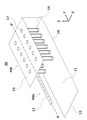
- a perspective view showing a mode conversion structure according to Embodiment 1 of the present disclosure A side cross-sectional view showing a mode conversion structure according to Embodiment 1 of the present disclosure
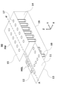
- a perspective view showing a mode conversion structure according to a comparative example (example based on existing technology)
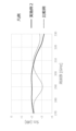
- Side sectional view showing a mode conversion structure according to a comparative example A diagram showing radiated power simulation results of a mode conversion structure according to Embodiment 1 of the present disclosure and a mode conversion structure according to a comparative example.
- a perspective view showing a mode conversion structure according to Embodiment 2 of the present disclosure A side sectional view showing a mode conversion structure according to Embodiment 2 of the present disclosure
- a perspective view showing a mode conversion structure according to a modification of Embodiment 2 of the present disclosure A side sectional view showing a mode conversion structure according to a modification of Embodiment 2 of the present disclosure
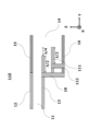
- a perspective view showing a mode conversion structure according to Embodiment 3 of the present disclosure A side sectional view showing a mode conversion structure according to Embodiment 3 of the present disclosure
- a side sectional view showing a mode conversion structure according to a modification of Embodiment 3 of the present disclosure A side sectional view showing a mode conversion structure according to a modification of Embodiment 3 of the present disclosure
- the Z-axis positive direction shown in the drawings is referred to as an upper (direction), and the Z-axis negative direction is referred to as a lower (direction).
- some elements such as side surfaces of the mode conversion structure (planes parallel to the YZ plane shown in the drawings) are omitted for ease of viewing, and some elements are shown to scale. There are some things that are not depicted in the image.
- FIG. 1 is a perspective view showing a mode conversion structure 10 according to Embodiment 1 of the present disclosure
- FIG. 2 is a side sectional view (AA' sectional view) showing the mode conversion structure 10.
- the mode conversion structure 10 includes a first dielectric substrate 11 having a microstrip line MSL and a second dielectric substrate 14 having a post wall waveguide PW.
- first thickness is different from the thickness of the second dielectric substrate 14 (second thickness).
- the thickness of the first dielectric substrate 11 may be read as the thickness of the dielectric material constituting the first dielectric substrate 11 or the thickness of the microstrip line MSL
- the thickness of the second dielectric substrate 14 may be read as the thickness of the dielectric material constituting the first dielectric substrate 11 or the thickness of the microstrip line MSL. It may also be read as the thickness of the dielectric constituting the two-dielectric substrate 14 or the thickness of the post wall waveguide PW.
- the first dielectric substrate 11 and the second dielectric substrate 14 may be composed of one substrate or may be composed of different substrates.
- the microstrip line MSL includes a first dielectric substrate 11, a line conductor 12, and GND 13 (first ground conductor). Specifically, the microstrip line MSL is configured by a line conductor 12 and GND 13 that face each other with a dielectric sandwiched therebetween on the first dielectric substrate 11 .
- the post wall waveguide PW includes a second dielectric substrate 14, a first conductor layer 15, a second conductor layer 16, and a via (via hole) 17.
- the post wall waveguide PW includes a first conductor layer 15 and a second conductor layer (waveguide wide wall or simply wide wall) that face each other with a dielectric sandwiched therebetween in the second dielectric substrate 14. 16 and opposing vias (waveguide narrow walls or simply narrow walls) 17 that electrically connect these conductor layers.
- the vias 17 are arranged in the signal transmission direction (electromagnetic wave propagation direction (transmission direction); Y direction) at intervals of less than a half wavelength ( ⁇ /2) of the electromagnetic wave.
- the line conductor 12 and the first conductor layer 15 are connected on the same plane (a plane parallel to the XY plane).
- the via (via hole) 18 (first via) electrically connects the GND 13 and the second conductor layer 16 (the GND 13 and the second conductor layer 16 electrically connected via). Therefore, unlike existing techniques, the GND 13 and the second conductor layer 16 are not connected on the same plane (a plane parallel to the XY plane).
- FIG. 3 is a perspective view showing a mode conversion structure 30 according to a comparative example
- FIG. 4 is a side sectional view (AA' sectional view) showing the mode conversion structure 30.
- the same elements as those in the mode conversion structure 10 are given the same reference numerals, and the parts different from the mode conversion structure 10 will be explained.
- the mode conversion structure 30 includes a first dielectric substrate 11 having a microstrip line MSL and a second dielectric substrate 14 having a post wall waveguide PW.
- the thickness of the first dielectric substrate 11 and the thickness of the second dielectric substrate 14 are the same, and the GND 13 and the second conductor layer 16 are arranged in the same plane (XY (plane), and there is no via corresponding to via 18. Therefore, the mode conversion structure 30 may be considered as an example of existing technology based on the mode conversion structure disclosed in Patent Document 1.
- FIG. 5 is a diagram showing the radiation power simulation results of the mode conversion structure 10 according to Example 1 and the mode conversion structure 30 according to the comparative example when a power of 0.5 W is input. From FIG. 5, it can be seen that the mode conversion structure 10 according to Example 1 radiates less power into space than the mode conversion structure 30 according to Comparative Example 1, and can reduce radiation loss. This is because the thickness of the microstrip line according to Example 1 is thinner than the thickness of the microstrip line according to the comparative example.
- the thickness of the microstrip line MSL does not need to be the same as the thickness of the post wall waveguide PW, so transmission loss can be suppressed, and the thickness of the microstrip line MSL can be suppressed.
- Line MSL and post wall waveguide PW can be connected.
- FIG. 6 is a perspective view showing a mode conversion structure 60 according to Embodiment 2 of the present disclosure
- FIG. 7 is a side sectional view (AA' sectional view) showing the mode conversion structure 60.
- the same elements as those in the mode conversion structure 10 are given the same reference numerals, and the parts different from the mode conversion structure 10 will be explained.
- the mode conversion structure 60 is arranged to extend (overlap) by about ⁇ /2.
- the GND 13 extends by about ⁇ /2 in the direction of the post wall waveguide PW (positive side of the Y-axis) with respect to the end face of the via 18 (ZX plane perpendicular to the Y-axis).
- the via 18 is arranged at a distance of about ⁇ /2 from the end surface (end) of the GND 13 in contact with the post wall waveguide PW along the electromagnetic wave propagation direction (in the negative direction of the Y axis) when viewed from the Z direction. ing.
- the GND 13 the first conductor layer 15, and the second conductor layer 16 are arranged to overlap by about ⁇ /2 in the YZ cross section.
- the end face of the GND 13 (the end face in contact with the post wall waveguide PW when viewed from the Z direction), the via 18, and the second conductor layer 16 form a short stub, which reduces the reflection of power and improves the transmission characteristics. Improve.
- FIG. 8 is a diagram showing the results of simulation of the transmission characteristics of the mode conversion structure 60 and the mode conversion structure 30.
- the horizontal axis represents the frequency (unit: GHz), and the vertical axis represents the value (unit: dB) of S21, which is an S parameter indicating the pass characteristic.
- the mode conversion structure 60 has a larger passing characteristic than the mode conversion structure 30.
- FIG. 9 is a perspective view showing a mode conversion structure 90 according to a modification of the second embodiment of the present disclosure
- FIG. 10 is a side sectional view (AA' sectional view) showing the mode conversion structure 90. .
- the post wall waveguide PW is extended by about ⁇ /2 in the direction of the microstrip line MSL (the negative direction of the Y axis) based on the ZX plane perpendicular to The positions of the GND 13 and the vias 18 in the direction are shifted by about ⁇ /2 in the negative direction of the Y axis.
- the line conductor 12, GND 13, and second conductor layer 16 are arranged to overlap by about ⁇ /2 in the YZ cross section.
- the via 18 extends from the end surface of the GND 13 in contact with the post wall waveguide PW, along the electromagnetic wave propagation direction (in the negative direction of the Y axis), when viewed from the Z direction (on the XY plane). are located some distance apart. Even with this structure, the end face of GND 13 (the end face in contact with post wall waveguide PW when viewed from the Z direction), the via 18, and the second conductor layer 16 constitute a short stub, so the reflection of power is reduced. , the passing characteristics are improved.
- the via 18 does not need to be placed directly under the position where the line conductor 12 of the microstrip line MSL and the first conductor layer 15 of the post wall waveguide PW are connected or in the vicinity thereof.
- the transmission characteristics depend on the positional relationship between the GND 13 of the microstrip line MSL, the second conductor layer 16 of the post wall waveguide PW, and the via 18.
- FIG. 11 is a perspective view showing a mode conversion structure 110 according to Embodiment 3 of the present disclosure
- FIG. 12 is a side sectional view (AA' sectional view) showing the mode conversion structure 110.
- the mode conversion structure 110 the same elements as those in the mode conversion structure 60 are given the same reference numerals, and portions different from the mode conversion structure 60 will be described.
- a GND 111 (second ground conductor) is provided between the GND 13 and the second conductor layer 16.
- Mode conversion structure 110 includes GND 111 disposed between GND 13 and second conductor layer 16 .
- the GND 111 extends about 3 ⁇ /4 along the electromagnetic wave propagation direction from the end face of the via 18 (the end face in contact with the post wall waveguide PW when seen from the Z direction) when viewed from the Z direction (on the XY plane). are doing.
- the end face of GND 13 (the end face in contact with the post wall waveguide PW when viewed from the Z direction) and the end face of GND 111 (the end face in contact with the post wall waveguide PW when seen from the Z direction) are They are separated by about ⁇ /4 along the propagation direction.
- the first conductor layer 15, GND 13 and the second conductor layer 16 are arranged to overlap by about ⁇ /2 in the YZ cross section, and the first conductor layer 15, GND 111 and the second conductor layer
- the layers 16 are arranged to overlap by about 3 ⁇ /4 in the YZ cross section, and the GNDs 111 and GND 13 are arranged to overlap by about ⁇ /2 in the YZ cross section.
- a via (via hole) 112 (second via) that electrically connects the GND 111 and the second conductor layer 16 is provided.
- the mode conversion structure 110 includes a via 112 that electrically connects the GND 111 and the second conductor layer 16.
- the via 112 extends from the end face of the GND 111 (the end face in contact with the post wall waveguide PW when seen from the Z direction) along the electromagnetic wave propagation direction (in the negative direction of the Y axis) by about ⁇ /2 when viewed from the Z direction. are located far apart.
- the short stub formed by the GND 13 and the via 18 and the short stub formed by the GND 111 and the via 112 are stacked in a stepped manner.
- the phases of the reflected waves from the respective short stubs can be made to be in opposite phases.
- the present inventors conducted an electromagnetic field simulation using a finite integral method to find a mode conversion structure 110 according to Example 3 (Embodiment 3) shown in FIG. 11 and a comparative example (example based on existing technology) shown in FIG. The transmission characteristics of the mode conversion structure 30 were analyzed and compared.
- FIG. 13 is a diagram showing the results of simulation of the transmission characteristics of the mode conversion structure 110 and the mode conversion structure 30.
- the horizontal axis represents the frequency (unit: GHz), and the vertical axis represents the value of S21 (unit: dB).
- the mode conversion structure 110 has a larger passing characteristic than the mode conversion structure 30.
- FIG. 11 and FIG. 12 show an example in which the short stubs are stacked in a two-stage staircase, there is no limit to the number of stages.
- FIG. 14 a side cross-sectional view (corresponding to the AA' cross-sectional view of other drawings) showing a mode conversion structure 140 according to a modification of the third embodiment of the present disclosure
- the GND 141 and the via 142 may be added, and the short stubs may be stacked in a three-tiered manner.
- GND and vias may be added in the same way, and the short stubs may be stacked in four or more steps.
- the mode conversion structure includes n (n is an integer of 1 or more) GNDs (GND111, GND141, etc.) disposed between GND13 and the second conductor layer 16, and each of the n GNDs and the It may also include vias (second vias; vias 112, vias 142, etc.) that electrically connect the two conductor layers 16.
- n is an integer of 1 or more GNDs (GND111, GND141, etc.) disposed between GND13 and the second conductor layer 16, and each of the n GNDs and the It may also include vias (second vias; vias 112, vias 142, etc.) that electrically connect the two conductor layers 16.
- the via 142 that electrically connects the GND 141 and the second conductor layer 16 extends from the end surface of the GND 141 (the end surface in contact with the post wall waveguide PW) along the propagation direction of electromagnetic waves when viewed from the Z direction. , may be arranged at a distance of about ⁇ /2.
- each opposing GND pair (the end faces in contact with the post wall waveguide PW) of (n+1) GNDs consisting of GND 13 and n GNDs are aligned along the propagation direction of electromagnetic waves when viewed from the Z direction. , may be separated by about ⁇ /4.
- the end faces of the opposing pair GND13 and GND111 (the end faces in contact with the post wall waveguide PW) are in the direction of electromagnetic wave propagation when viewed from the Z direction. They may be separated by about ⁇ /4 along the direction.
- the opposing pair GND111 and GND141 have their end faces (end faces in contact with the post wall waveguide PW) separated by about ⁇ /4 along the electromagnetic wave propagation direction when viewed from the Z direction. You can.
- the first conductor layer 15, GND 13, and second conductor layer 16 are arranged to overlap by about ⁇ /2 in the YZ cross section, and the first conductor layer 15, GND 111, and second conductor layer
- the layers 16 are arranged to overlap by about 3 ⁇ /4 in the YZ cross section, the first conductor layer 15, GND 141 and the second conductor layer 16 are arranged to overlap by about ⁇ in the YZ cross section, and the GND 111 and GND 13 are In the YZ cross section, the GND 111 and GND 141 are arranged to overlap by about ⁇ /2, and the GND 111 and GND 141 are arranged to overlap by about 3 ⁇ /4 in the YZ cross section.
- the mode conversion structure (mode conversion structure 10, 60, 90, 110, 140) according to the embodiment of the present disclosure has a microstrip line MSL configured by opposing line conductors 12 and GND 13, and has a first thickness.
- a second dielectric substrate 14 having a post wall waveguide PW including a first conductor layer 15 and a second conductor layer 16 facing each other, and having a second thickness that is thicker than the first thickness. and a via 18 that electrically connects the GND 13 and the second conductor layer 16.
- the line conductor 12 and the first conductor layer 15 are connected on the same plane (a plane parallel to the XY plane).
- the thickness of the microstrip line does not need to be the same as the thickness of the post wall waveguide, so transmission loss can be suppressed and it is possible to connect the microstrip line and the post wall waveguide with different thicknesses. can.
- a waveguide includes a microstrip line configured by a line conductor and a first ground conductor facing the line conductor, and a first dielectric substrate having a first thickness.
- a post wall waveguide including a first conductor layer connected on the same plane as the line conductor, and a second conductor layer facing the first conductor layer, and a second conductor layer having a thickness greater than the first thickness.
- the device includes a second dielectric substrate having a thickness, and a first via that electrically connects the first ground conductor and the second conductor layer.
- the thickness of the microstrip line does not need to be the same as the thickness of the post wall waveguide, so transmission loss can be suppressed, and it is possible to connect the microstrip line and the post wall waveguide with different thicknesses. I can do it.
- the first via is configured to transmit electromagnetic waves propagating through the post wall waveguide from an end of the first ground conductor in contact with the post wall waveguide when viewed from a direction perpendicular to the same plane.
- the electromagnetic waves are spaced apart from each other by approximately half a wavelength of the electromagnetic waves along the propagation direction.
- the end of the first ground conductor, the first via, and the second conductor layer form a short stub, which reduces reflection of power and improves transmission characteristics.
- This mode conversion structure includes a second ground conductor disposed between the first ground conductor and the second conductor layer, and a second ground conductor that electrically connects the second ground conductor and the second conductor layer.
- the second via extends from the end of the second ground conductor in contact with the post wall waveguide along the propagation direction when viewed from a direction perpendicular to the same plane.
- the end portion of the first ground conductor that is in contact with the post wall waveguide and the end portion of the second ground conductor that is in contact with the post wall waveguide are disposed approximately half a wavelength of electromagnetic waves apart, and that the end portion of the first ground conductor that is in contact with the post wall waveguide is on the same plane. When viewed in the vertical direction, they are separated by approximately a quarter wavelength of the electromagnetic waves.
- the short stubs are stacked and the reflected waves from the short stubs are canceled, so it is possible to reduce loss due to reflection and further improve the transmission characteristics.
- This mode conversion structure includes n ground conductors (n is an integer of 1 or more) disposed between the first ground conductor and the second conductor layer, and each of the n ground conductors and the a second via electrically connecting the second conductor layer, the second via being connected to the n ground conductors in contact with the post wall waveguide when viewed from a direction perpendicular to the same plane. along the propagation direction from each end of the electromagnetic wave by approximately half a wavelength of the electromagnetic wave.
- an end in contact with the post wall waveguide among the ends of each opposing ground conductor pair of (n+1) ground conductors including the first ground conductor and the n ground conductors. are separated by approximately a quarter wavelength of the electromagnetic waves when viewed from a direction perpendicular to the same plane.
- the reflected waves from the short stub are canceled, so it is possible to reduce loss due to reflection and further improve the transmission characteristics.
- the first ground conductor, the first conductor layer, and the second conductor layer are arranged along the propagation direction of the electromagnetic wave propagating in the post wall waveguide.
- the electromagnetic waves are arranged so as to overlap approximately half the wavelength of the electromagnetic waves.
- the first ground conductor, the line conductor, and the second conductor layer are arranged along the propagation direction of the electromagnetic wave propagating in the post wall waveguide. They are arranged to overlap approximately half the wavelength of the electromagnetic waves.
- An embodiment of the present disclosure is useful for a mode conversion structure for connecting a microstrip line and a post wall waveguide.
- Mode conversion structure 11 First dielectric substrate 12 Line conductor 13 Ground conductor 14 Second dielectric substrate 15 First conductor layer 16 Second conductor layer 17 Via (via hole) 18 Via (Beer Hall) 30 Mode conversion structure 60 Mode conversion structure 90 Mode conversion structure 110 Mode conversion structure 111 Ground conductor 112 Via (via hole) 140 Mode conversion structure 141 Ground conductor 142 Via (via hole)
Landscapes
- Waveguides (AREA)
Priority Applications (3)
| Application Number | Priority Date | Filing Date | Title |
|---|---|---|---|
| JP2024522901A JPWO2023228456A1 (https=) | 2022-05-26 | 2022-12-22 | |
| US18/857,086 US20250253510A1 (en) | 2022-05-26 | 2022-12-22 | Mode conversion device |
| CN202280095657.3A CN119137804A (zh) | 2022-05-26 | 2022-12-22 | 模式转换结构 |
Applications Claiming Priority (2)
| Application Number | Priority Date | Filing Date | Title |
|---|---|---|---|
| JP2022-085966 | 2022-05-26 | ||
| JP2022085966 | 2022-05-26 |
Publications (1)
| Publication Number | Publication Date |
|---|---|
| WO2023228456A1 true WO2023228456A1 (ja) | 2023-11-30 |
Family
ID=88918901
Family Applications (1)
| Application Number | Title | Priority Date | Filing Date |
|---|---|---|---|
| PCT/JP2022/047315 Ceased WO2023228456A1 (ja) | 2022-05-26 | 2022-12-22 | モード変換構造 |
Country Status (4)
| Country | Link |
|---|---|
| US (1) | US20250253510A1 (https=) |
| JP (1) | JPWO2023228456A1 (https=) |
| CN (1) | CN119137804A (https=) |
| WO (1) | WO2023228456A1 (https=) |
Citations (2)
| Publication number | Priority date | Publication date | Assignee | Title |
|---|---|---|---|---|
| JP2011139244A (ja) * | 2009-12-28 | 2011-07-14 | Kyocera Corp | 高周波モジュール |
| JP2016111459A (ja) * | 2014-12-04 | 2016-06-20 | アンリツ株式会社 | ミリ波帯伝送路変換構造 |
Family Cites Families (2)
| Publication number | Priority date | Publication date | Assignee | Title |
|---|---|---|---|---|
| US9405064B2 (en) * | 2012-04-04 | 2016-08-02 | Texas Instruments Incorporated | Microstrip line of different widths, ground planes of different distances |
| DE102015221142A1 (de) * | 2014-10-31 | 2016-05-19 | Anritsu Corporation | Übertragungsleitungs-Umwandlungsstruktur für ein Millimeterwellenband |
-
2022
- 2022-12-22 CN CN202280095657.3A patent/CN119137804A/zh active Pending
- 2022-12-22 JP JP2024522901A patent/JPWO2023228456A1/ja active Pending
- 2022-12-22 US US18/857,086 patent/US20250253510A1/en active Pending
- 2022-12-22 WO PCT/JP2022/047315 patent/WO2023228456A1/ja not_active Ceased
Patent Citations (2)
| Publication number | Priority date | Publication date | Assignee | Title |
|---|---|---|---|---|
| JP2011139244A (ja) * | 2009-12-28 | 2011-07-14 | Kyocera Corp | 高周波モジュール |
| JP2016111459A (ja) * | 2014-12-04 | 2016-06-20 | アンリツ株式会社 | ミリ波帯伝送路変換構造 |
Also Published As
| Publication number | Publication date |
|---|---|
| CN119137804A (zh) | 2024-12-13 |
| JPWO2023228456A1 (https=) | 2023-11-30 |
| US20250253510A1 (en) | 2025-08-07 |
Similar Documents
| Publication | Publication Date | Title |
|---|---|---|
| US6674347B1 (en) | Multi-layer substrate suppressing an unwanted transmission mode | |
| CN102414920B (zh) | 结构体、印刷板、天线、传输线波导转换器、阵列天线和电子装置 | |
| JP4568235B2 (ja) | 伝送路変換器 | |
| JP2004153367A (ja) | 高周波モジュール、ならびにモード変換構造および方法 | |
| CN103120038B (zh) | 结构体和配线基板 | |
| US9214715B2 (en) | Hybrid coupler device having plural transmission line structures with unwound-rewound geometry | |
| US9456499B2 (en) | Structural body and interconnect substrate | |
| JP7702696B2 (ja) | 導波路 | |
| JP7598490B2 (ja) | 伝送線路 | |
| WO2023228456A1 (ja) | モード変換構造 | |
| JP2005051330A (ja) | 誘電体導波管線路と高周波伝送線路との接続構造およびそれを用いた高周波回路基板ならびに高周波素子搭載用パッケージ | |
| JP2019106663A (ja) | 高周波回路 | |
| JP7077137B2 (ja) | 伝送線路およびコネクタ | |
| JP2009094752A (ja) | 高周波伝送線路 | |
| WO2024009339A1 (ja) | マイクロストリップ線路-導波管変換器 | |
| JPH04122106A (ja) | マイクロストリップアンテナ | |
| JP7555523B2 (ja) | マイクロストリップ線路-導波管変換器 | |
| JP6491080B2 (ja) | 多層配線基板 | |
| JP3895716B2 (ja) | 高周波伝送基板および高周波伝送基板接続構造 | |
| JP4542531B2 (ja) | 伝送モードの変換構造 | |
| WO2024257199A1 (ja) | 導波管の接続構造 | |
| KR20250169728A (ko) | 임피던스 정합을 수행하는 안테나 시스템 | |
| JP2023136491A (ja) | 平面線路・導波管変換器 | |
| JP2016127511A (ja) | 導波路変換構造体 | |
| CN114503359A (zh) | 高频封装 |
Legal Events
| Date | Code | Title | Description |
|---|---|---|---|
| 121 | Ep: the epo has been informed by wipo that ep was designated in this application |
Ref document number: 22943855 Country of ref document: EP Kind code of ref document: A1 |
|
| WWE | Wipo information: entry into national phase |
Ref document number: 18857086 Country of ref document: US |
|
| WWE | Wipo information: entry into national phase |
Ref document number: 202280095657.3 Country of ref document: CN Ref document number: 2024522901 Country of ref document: JP |
|
| NENP | Non-entry into the national phase |
Ref country code: DE |
|
| 122 | Ep: pct application non-entry in european phase |
Ref document number: 22943855 Country of ref document: EP Kind code of ref document: A1 |
|
| WWP | Wipo information: published in national office |
Ref document number: 18857086 Country of ref document: US |