WO2023224091A1 - 熱電変換素子及び熱電変換デバイス - Google Patents
熱電変換素子及び熱電変換デバイス Download PDFInfo
- Publication number
- WO2023224091A1 WO2023224091A1 PCT/JP2023/018578 JP2023018578W WO2023224091A1 WO 2023224091 A1 WO2023224091 A1 WO 2023224091A1 JP 2023018578 W JP2023018578 W JP 2023018578W WO 2023224091 A1 WO2023224091 A1 WO 2023224091A1
- Authority
- WO
- WIPO (PCT)
- Prior art keywords
- thermoelectric conversion
- conversion element
- substrate
- conversion elements
- magnetization
- Prior art date
- Legal status (The legal status is an assumption and is not a legal conclusion. Google has not performed a legal analysis and makes no representation as to the accuracy of the status listed.)
- Ceased
Links
Images




Classifications
-
- H—ELECTRICITY
- H10—SEMICONDUCTOR DEVICES; ELECTRIC SOLID-STATE DEVICES NOT OTHERWISE PROVIDED FOR
- H10N—ELECTRIC SOLID-STATE DEVICES NOT OTHERWISE PROVIDED FOR
- H10N15/00—Thermoelectric devices without a junction of dissimilar materials; Thermomagnetic devices, e.g. using the Nernst-Ettingshausen effect
-
- H—ELECTRICITY
- H10—SEMICONDUCTOR DEVICES; ELECTRIC SOLID-STATE DEVICES NOT OTHERWISE PROVIDED FOR
- H10N—ELECTRIC SOLID-STATE DEVICES NOT OTHERWISE PROVIDED FOR
- H10N15/00—Thermoelectric devices without a junction of dissimilar materials; Thermomagnetic devices, e.g. using the Nernst-Ettingshausen effect
- H10N15/20—Thermomagnetic devices using thermal change of the magnetic permeability, e.g. working above and below the Curie point
-
- H—ELECTRICITY
- H10—SEMICONDUCTOR DEVICES; ELECTRIC SOLID-STATE DEVICES NOT OTHERWISE PROVIDED FOR
- H10N—ELECTRIC SOLID-STATE DEVICES NOT OTHERWISE PROVIDED FOR
- H10N19/00—Integrated devices, or assemblies of multiple devices, comprising at least one thermoelectric or thermomagnetic element covered by groups H10N10/00 - H10N15/00
-
- H—ELECTRICITY
- H01—ELECTRIC ELEMENTS
- H01F—MAGNETS; INDUCTANCES; TRANSFORMERS; SELECTION OF MATERIALS FOR THEIR MAGNETIC PROPERTIES
- H01F10/00—Thin magnetic films, e.g. of one-domain structure
- H01F10/08—Thin magnetic films, e.g. of one-domain structure characterised by magnetic layers
- H01F10/10—Thin magnetic films, e.g. of one-domain structure characterised by magnetic layers characterised by the composition
- H01F10/12—Thin magnetic films, e.g. of one-domain structure characterised by magnetic layers characterised by the composition being metals or alloys
- H01F10/126—Thin magnetic films, e.g. of one-domain structure characterised by magnetic layers characterised by the composition being metals or alloys containing rare earth metals
Definitions
- the present invention relates to a thermoelectric conversion element and a thermoelectric conversion device.
- thermoelectric modules that convert temperature differences between objects into voltage have been those that use the Seebeck effect.
- thermoelectric modules using the anomalous Nernst effect are attracting great interest because of their simple structure and versatility of materials, although their performance index is inferior to that of the Seebeck effect (see, for example, Patent Document 1).
- the anomalous Nernst effect generally occurs in ferromagnetic materials, it reacts strongly to external magnetic fields. Furthermore, in ferromagnetic materials, it is difficult to produce the anomalous Nernst effect in zero magnetic field regardless of the shape. Therefore, for stable use of thermoelectric modules that utilize the anomalous Nernst effect, it is extremely important to use materials that do not easily react to external magnetic fields.
- the present invention has been made in view of the above problems, and an object of the present invention is to provide a thermoelectric conversion element and a thermoelectric conversion device that are stable against external magnetic fields.
- thermoelectric conversion element according to the first aspect of the present invention is made of a material that can be magnetized in any direction in a zero magnetic field, and exhibits an anomalous Nernst effect.
- thermoelectric conversion device includes a substrate and a plurality of thermoelectric conversion elements provided on the substrate and each having a shape extending in one direction.
- the plurality of thermoelectric conversion elements are arranged in parallel in a direction orthogonal to one direction, electrically connected in series, made of a material that can be magnetized in any direction in a zero magnetic field, and exhibit an anomalous Nernst effect.
- thermoelectric conversion device includes a first substrate and a plurality of first thermoelectric conversion elements provided on the first substrate each extending in one direction, the first thermoelectric conversion elements each having a shape extending in one direction.
- a plurality of first thermoelectric conversion elements that are arranged in parallel in a direction orthogonal to the first one are made of a first material that can be magnetized in any direction in a zero magnetic field, and exhibit an abnormal Nernst effect;
- a plurality of second thermoelectric conversion elements are made of a material and exhibit an abnormal Nernst effect.
- the first material and the second material have Nernst coefficients with opposite signs, and the plurality of first thermoelectric conversion elements and the plurality of second thermoelectric conversion elements are alternately electrically connected
- thermoelectric conversion by using a material that exhibits the anomalous Nernst effect and can be magnetized in any direction in a zero magnetic field, it is possible to realize thermoelectric conversion that is stable against external magnetic fields.
- FIG. 2 is a schematic diagram for explaining a thermoelectric mechanism using a thermoelectric conversion element according to the present embodiment. It is a graph showing the temperature dependence of the Hall resistivity of GdCo 3 , Gd 2 Co 7 and GdCo 5 , and the temperature dependence of the magnetization of Gd 2 Co 7 .
- FIG. 2 is a schematic diagram showing the crystal structure of Gd 2 Co type 7 .
- FIG. 2 is a schematic diagram showing the crystal structure of Ce 2 Ni type 7 . It is a graph showing the magnetic field dependence of the Nernst coefficient of Gd 2 Co 7 single crystal. It is a graph showing the magnetic field dependence of the Nernst coefficient of Ho 1.2 Gd 0.8 Co 7 single crystal.
- FIG. 1 is a perspective view showing the configuration of a thermoelectric conversion device according to Example 1 of the present embodiment. It is a schematic diagram which shows the structure of the 1st structure of the thermoelectric conversion device based on Example 2 of this embodiment. It is a schematic diagram which shows the structure of the 2nd structure of the thermoelectric conversion device based on Example 2 of this embodiment. 3 is a schematic diagram showing the configuration of a thermoelectric conversion device according to Example 2.
- FIG. 3 is a schematic external view of a thermoelectric conversion device according to Example 2.
- FIG. 3 is a schematic external view of a thermoelectric conversion device according to Example 2.
- thermoelectric conversion element and its thermoelectric mechanism according to an embodiment of the present invention will be described.
- the thermoelectric conversion element 1 As shown in FIG. 1, the thermoelectric conversion element 1 according to the present embodiment has a rectangular parallelepiped shape extending in one direction (y direction), has a predetermined thickness (length in the z direction), and has a predetermined thickness (length in the z direction). Assume that it is magnetized to .
- a heat flow Q ( ⁇ T) in the +x direction flows through the thermoelectric conversion element 1, a temperature difference occurs in the +x direction.
- the thermoelectric conversion element 1 due to the abnormal Nernst effect, the thermoelectric conversion element 1 generates an electromotive force V ( ⁇ M ⁇ (- ⁇ T)) occurs.
- the object is a thermoelectric conversion element that is made of a material that can be magnetized in any direction in a zero magnetic field and that exhibits the anomalous Nernst effect.
- the shape magnetic anisotropy must be small.
- the magnetization must be small, and it is desirable that the magnetization be 2 kG (kilogauss) or less, and more preferably 1 kG or less, at the temperature of the actual usage environment.
- the ferrimagnetic material has a magnetization compensation temperature Tk , and the relative magnitudes of the magnetization of the two types of sublattices change before and after Tk . Therefore, the magnetization of the ferrimagnetic material is relatively small near Tk , and the shape magnetic anisotropy becomes weak. As a result, unlike ferromagnetic materials, ferrimagnetic materials have stable magnetization and can be oriented in any direction. In this way, when the magnetization is small, the thin wire can be stably oriented in any direction such as perpendicular to the longitudinal direction or diagonally.
- FIG. 2 shows the temperature dependence of the Hall resistivity of GdCo 3 single crystal, Gd 2 Co 7 single crystal, and GdCo 5 single crystal, and the temperature dependence of magnetization of Gd 2 Co 7 single crystal.
- FIG. 2 is based on the following document. Ogawa A, Katayama T, Hirano M, et al. General Treatment of Anomalous Hall Effect and Kerr Rotation in Rare Earth Cobalt Systems[J]. Japanese Journal of Applied Physics, 1976, 15(S1): 87.
- Gd 2 Co 7 which is a ferrimagnetic material
- the magnetization of Gd (upward arrow) and Co (downward arrow) are in opposite directions, and at a temperature lower than T k , Gd becomes Co
- Gd has a smaller magnetization than Co at temperatures higher than Tk .
- the magnetizations of Gd and Co are balanced, and the magnetization of Gd 2 Co 7 (black circle) becomes zero.
- the sign of the Hall resistivity (white circle) of Gd 2 Co 7 is reversed at Tk .
- the sign of the anomalous Hall effect Hall resistivity
- the sign of the anomalous Nernst effect Neernst coefficient
- FIGS. 3A and 3B there are two crystal structures of R 2 Co 7 : a rhombohedral Gd 2 Co 7 -type structure and a hexagonal Ce 2 Ni 7 -type structure.
- the space group is P6 3 /mmc
- the c-axis length of the rhombohedral crystal system is about 1.5 times that of the hexagonal crystal system.
- Ce 2 Co 7 , Pr 2 Co 7 , Sm 2 Co 7 , and Gd 2 Co 7 can have both rhombohedral and hexagonal structures.
- FIG. 4A shows the magnetic field dependence of the Nernst coefficient of a Gd 2 Co 7 single crystal at 300 K when a magnetic field parallel to the c-axis is applied.
- FIG. 4B shows the magnetic field dependence of the Nernst coefficient of the Ho 1.2 Gd 0.8 Co 7 single crystal at 300 K when a magnetic field parallel to the c-axis is applied.
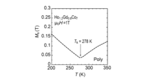
- FIG. 4C shows the temperature dependence of the magnetization of Ho 1.2 Gd 0.8 Co 7 when a magnetic field of 1 T is applied.
- the T k of Gd 2 Co 7 is well above room temperature (see Table 1).
- T k of Ho 1.2 Gd 0.8 Co 7 is 278 K, which is lower than room temperature.
- FIG. 4D shows the temperature dependence of magnetization of Gd 2 Co 7 , GdCo 2 , GdCo 3 , GdCo 5 , Gd 2.2 Co 16.6 , and Gd 2 Co 17 .
- FIG. 4D is based on the following document: Katayama T, Shibata T, Magnetic properties of some gadolinium-Cobalt intermetallic compounds[J]. Journal of Magnetism and Magnetic Materials, 1981, 23(2): 173-182.
- the magnetization value of the ferrimagnetic material Gd 2 Co 7 is one-fifth to one-tenth that of a ferromagnetic material such as GdCo 5 .
- the magnetization value can be further reduced. Specifically, if another rare earth element is added to R 2 Co 7 , such as Ho 1.2 Gd 0.8 Co 7 shown in FIGS. 4B and 4C, a ternary compound with even lower magnetization can be obtained. be able to. That is, it is possible to obtain a ternary compound with low magnetization whose compositional formula is R1 2-x R2 x Co 7 (0 ⁇ x ⁇ 2, R1 and R2 are different rare earth elements).
- thermoelectric conversion element 1 which is made of a material such as ferrimagnetic material that can be magnetized in any direction in a zero magnetic field and exhibits the anomalous Nernst effect, it is possible to However, it becomes possible to realize a stable thermoelectric mechanism.
- thermoelectric conversion devices according to Examples 1 and 2 in which the thermoelectric conversion element 1 of this embodiment is modularized, will be described.
- FIG. 5 shows an external configuration of a thermoelectric conversion device 100 according to Example 1 of this embodiment.
- the thermoelectric conversion device 100 includes a substrate 22 and a power generation body 23 placed on the substrate 22.
- a heat flow Q flows from the substrate 22 side toward the power generation body 23
- a temperature difference occurs in the heat flow direction in the power generation body 23
- a voltage V is generated in the power generation body 23 due to the abnormal Nernst effect.
- the substrate 22 has a first surface 22a on which the power generator 23 is placed, and a second surface 22b opposite to the first surface 22a. Heat from a heat source (not shown) is applied to the second surface 22b.
- Examples of the material for the substrate 22 include MgO, Si, SiO2 , Al2O3 , etc. , but are not particularly limited.
- the power generating body 23 includes a plurality of first thermoelectric conversion elements 24 and a plurality of second thermoelectric conversion elements 25, each of which has an L-shaped three-dimensional shape of the same size.
- the first thermoelectric conversion element 24 and the second thermoelectric conversion element 25 have Nernst coefficients of opposite signs and are made of a first material and a second material, respectively, which can be magnetized in any direction in a zero magnetic field.
- the first material and the second material are different ferrimagnetic materials.
- Gd 2 Co 7 FIG. 4A
- Ho 1.2 Gd 0.8 Co 7 FIG. 4B
- the plurality of first thermoelectric conversion elements 24 and the plurality of second thermoelectric conversion elements 25 are arranged alternately on the substrate 22 in a direction (y direction) perpendicular to each longitudinal direction (x direction). are arranged in parallel. Further, the first thermoelectric conversion element 24 and the second thermoelectric conversion element 25 are arranged so that the directions of their magnetization M1 and magnetization M2 are the same. Note that the number of first thermoelectric conversion elements 24 and second thermoelectric conversion elements 25 that constitute the power generation body 23 is not limited.
- the +x side end of one side surface (+y side) in the longitudinal direction (x direction) of the first thermoelectric conversion element 24 is the first end surface 24a, and the ⁇ x side end of the other side surface ( ⁇ y side) This section is defined as the second end surface 24b.
- the end on the ⁇ x side of one side surface (+y side) in the longitudinal direction (x direction) of the second thermoelectric conversion element 25 is the first end surface 25a, and the end on the +x side of the other side surface ( ⁇ y side) This section is defined as the second end surface 25b.
- thermoelectric conversion element 25 and the second end surface 24b of the first thermoelectric conversion element 24 adjacent to the +y side are connected, and the second end surface 25b of the second thermoelectric conversion element 25 and the opposite side ( -y side) of the first thermoelectric conversion element 24 is connected to the first end face 24a of the first thermoelectric conversion element 24.
- the plurality of first thermoelectric conversion elements 24 and the plurality of second thermoelectric conversion elements 25 are electrically connected in series. That is, the power generation body 23 is provided in a meandering manner on the first surface 22a of the substrate 22.
- the first thermoelectric conversion element 24 and the second thermoelectric conversion element 25 are insulated from each other except for their connection points.
- a heat flow Q flows in the +z direction toward the power generating body 23.
- the abnormal Nernst effect causes the first thermoelectric conversion element 24 to generate a temperature difference in a direction (-x direction) perpendicular to both the direction of the magnetization M1 (-y direction) and the direction of the heat flow Q (+z direction).
- an electromotive force E1 is generated.
- an electromotive force E2 is generated in a direction (+x direction) perpendicular to both the direction of magnetization M2 (-y direction) and the direction of heat flow Q (+z direction) due to the abnormal Nernst effect.
- thermoelectric conversion element 24 and the second thermoelectric conversion element 25 arranged in parallel are electrically connected in series, the electromotive force E1 generated in the first thermoelectric conversion element 24 is , may be applied to the adjacent second thermoelectric conversion element 25. Furthermore, since the electromotive force E1 generated by the first thermoelectric conversion element 24 and the electromotive force E2 generated by the adjacent second thermoelectric conversion element 25 are in opposite directions, the adjacent first thermoelectric conversion element 24 and the second thermoelectric conversion element The electromotive force is added in each of the conversion elements 25, and the output voltage V can be increased.
- Example 2 of this embodiment will be described with reference to FIGS. 6A to 8.
- Example 1 deals with a thermoelectric conversion device 100 in which a first thermoelectric conversion element 24 and a second thermoelectric conversion element 25 having Nernst coefficients of opposite signs are provided on the same surface of a substrate 22.
- Example 2 a thermoelectric conversion device in which two types of such thermoelectric conversion elements are provided on separate substrates is targeted.
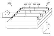
- the thermoelectric conversion device includes a first structure 201 shown in FIG. 6A and a second structure 202 shown in FIG. 6B.
- the first structure 201 includes a first substrate 210 and a plurality of rectangular parallelepiped-shaped first thermoelectric conversion elements 231 to 231 of the same size provided on the first surface 211 of the first substrate 210. 234.
- the first thermoelectric conversion elements 231 to 234 are arranged in parallel at equal intervals in a direction perpendicular to the longitudinal direction.
- the second structure 202 includes a second substrate 220 and a plurality of second thermoelectric conversion elements 241 to 244 provided on the first surface 221 of the second substrate 220. .
- the second thermoelectric conversion elements 241 to 244 have the same shape and size as the first thermoelectric conversion elements 231 to 234, and are arranged in parallel at equal intervals in a direction perpendicular to the longitudinal direction. These thermoelectric conversion elements are formed on a substrate by, for example, a sputtering method. Materials for the first substrate 210 and the second substrate 220 include MgO, Si, SiO 2 , Al 2 O 3 and the like, but are not particularly limited.
- the first thermoelectric conversion elements 231 to 234 are made of a first material
- the second thermoelectric conversion elements 241 to 244 are made of a second material.
- the first material and the second material have Nernst coefficients of opposite signs and can be magnetized in any direction in a zero magnetic field, and are, for example, different ferrimagnetic materials.
- Gd 2 Co 7 (FIG. 4A) can be used as the first material
- Ho 1.2 Gd 0.8 Co 7 (FIG. 4B) can be used as the second material.
- thermoelectric conversion elements 231 to 234 are arranged on the first substrate 210, and four second thermoelectric conversion elements 241 to 244 are arranged on the second substrate 220.
- the number of thermoelectric conversion elements on each substrate is not limited.
- a through hole passing through the first substrate 210 is provided in the vicinity of one or both ends of each first thermoelectric conversion element in the longitudinal direction. Specifically, as shown in FIG. 7, a through hole 272 is formed near one end of the first thermoelectric conversion element 231, through holes 273 and 274 are formed near both ends of the first thermoelectric conversion element 232, and both ends of the first thermoelectric conversion element 233 are formed. Through holes 275 and 276 are provided nearby, and through holes 277 and 278 are provided near both ends of the first thermoelectric conversion element 234.
- a through hole passing through the second substrate 220 is provided in the vicinity of one or both ends of each second thermoelectric conversion element in the longitudinal direction.
- through holes 281 and 282 are formed near both ends of the second thermoelectric conversion element 241
- through holes 283 and 284 are formed near both ends of the second thermoelectric conversion element 242
- the second thermoelectric conversion element 243 Through holes 285 and 286 are provided near both ends of the thermoelectric conversion element 244
- a through hole 287 is provided near one end of the second thermoelectric conversion element 244 .
- a conductive wire 204 passes through each through hole of the first substrate 210 and the second substrate 220.
- a first terminal and a second terminal are provided at both ends of each first thermoelectric conversion element, and a first terminal and a second terminal are provided at both ends of each second thermoelectric conversion element.
- a conducting wire 204 is connected to these first and second terminals.
- the second surface 212 of the first substrate 210 and the second surface 222 of the second substrate 220 are pasted together with an adhesive to form a thermoelectric conversion device 200 as shown in FIG.
- the second terminal 252 of the first thermoelectric conversion element 231 is connected to the first terminal 261 of the second thermoelectric conversion element 241 via through holes 272 and 281, and
- the second terminal 262 is connected to the first terminal 253 of the first thermoelectric conversion element 232 via through holes 282 and 273, and the second terminal 254 of the first thermoelectric conversion element 232 is connected to the first terminal 253 of the first thermoelectric conversion element 232 via through holes 274 and 283.
- the second terminal 264 of the second thermoelectric conversion element 242 is connected to the first terminal 255 of the first thermoelectric conversion element 233 via through holes 284 and 275.
- the second terminal 256 of the first thermoelectric conversion element 233 is connected to the first terminal 265 of the second thermoelectric conversion element 243 via the through holes 276 and 285, and the second terminal 256 of the second thermoelectric conversion element 243 is connected to the first terminal 265 of the second thermoelectric conversion element 243.
- thermoelectric conversion elements 231 to 234 and the second thermoelectric conversion elements 241 to 244 are alternately electrically connected in series. Furthermore, in FIGS. 7 and 8, the magnetization of the first thermoelectric conversion elements 231 to 234 and the magnetization of the second thermoelectric conversion elements 241 to 244 are oriented in the same direction (+y direction).
- thermoelectric conversion device 200 when a heat flow Q in the +z direction flows through the thermoelectric conversion device 200 and a temperature difference occurs due to the heat flow Q, an electromotive force is generated in the +x direction in the first thermoelectric conversion elements 231 to 234 due to the abnormal Nernst effect, and the second thermoelectric conversion An electromotive force is generated in the -x direction in the elements 241 to 244.
- the electromotive force generated in each thermoelectric conversion element is added, and a voltage V generated between the first terminal 251 of the first thermoelectric conversion element 231 and the second terminal 268 of the second thermoelectric conversion element 244 is output. can do.
- Example 2 a first thermoelectric conversion element and a second thermoelectric conversion element having mutually opposite signs of Nernst coefficients are formed on separate substrates, and the first structure 201 and the second structure 202 are manufactured.
- the thermoelectric conversion device 200 can be manufactured by a simple process. Moreover, the density of the thermoelectric conversion elements is about 2, compared to the thermoelectric conversion device 100 in which the first thermoelectric conversion element 24 and the second thermoelectric conversion element 25 are provided on the same surface of the substrate 22 as in Example 1 (FIG. 5). Since the output voltage is doubled, it is possible to increase the output voltage.
- the second surface 212 of the first substrate 210 and the second surface 222 of the second substrate 220 are pasted together, and the first surface 211 of the first substrate 210 and the second surface 222 of the second substrate 220 are bonded together.
- the first surfaces 221 face in opposite directions
- a configuration may be adopted in which the first surfaces 211 and 221 face in the same direction.
- thermoelectric conversion elements 231 to 234 on the first substrate 210 and the second thermoelectric conversion elements 241 to 244 on the second substrate 220 are connected in series by the conducting wire 204, the conducting wire 204 It may also pass through the outside of the second substrate 220.
- thermoelectric conversion element 22 substrate 23 power generation body 24, 231, 232, 233, 234 first thermoelectric conversion element 25, 241, 242, 243, 244 second thermoelectric conversion element 100, 200 thermoelectric conversion device 201 first structure 202 2 structure 204 conductive wire 210 first substrate 211 first surface 212 second surface 220 second substrate 221 first surface 222 second surface 251, 253, 255, 257, 261, 263, 265, 267 first terminal 252, 254 , 256, 258, 262, 264, 266, 268 2nd terminal 272-278, 281-287 Through hole
Landscapes
- Hall/Mr Elements (AREA)
Priority Applications (3)
| Application Number | Priority Date | Filing Date | Title |
|---|---|---|---|
| JP2024521976A JPWO2023224091A1 (https=) | 2022-05-18 | 2023-05-18 | |
| EP23807692.1A EP4529406A1 (en) | 2022-05-18 | 2023-05-18 | Thermoelectric conversion element and thermoelectric conversion device |
| US18/865,868 US20250324910A1 (en) | 2022-05-18 | 2023-05-18 | Thermoelectric conversion element and thermoelectric conversion device |
Applications Claiming Priority (2)
| Application Number | Priority Date | Filing Date | Title |
|---|---|---|---|
| JP2022-081825 | 2022-05-18 | ||
| JP2022081825 | 2022-05-18 |
Publications (1)
| Publication Number | Publication Date |
|---|---|
| WO2023224091A1 true WO2023224091A1 (ja) | 2023-11-23 |
Family
ID=88835279
Family Applications (1)
| Application Number | Title | Priority Date | Filing Date |
|---|---|---|---|
| PCT/JP2023/018578 Ceased WO2023224091A1 (ja) | 2022-05-18 | 2023-05-18 | 熱電変換素子及び熱電変換デバイス |
Country Status (4)
| Country | Link |
|---|---|
| US (1) | US20250324910A1 (https=) |
| EP (1) | EP4529406A1 (https=) |
| JP (1) | JPWO2023224091A1 (https=) |
| WO (1) | WO2023224091A1 (https=) |
Citations (5)
| Publication number | Priority date | Publication date | Assignee | Title |
|---|---|---|---|---|
| JPS5735657A (en) * | 1980-08-11 | 1982-02-26 | Fujitsu Ltd | Material for temperature sensitive element |
| JP2013522861A (ja) * | 2011-02-22 | 2013-06-13 | パナソニック株式会社 | 熱電変換素子とその製造方法 |
| JP2021128998A (ja) | 2020-02-13 | 2021-09-02 | 日本電気株式会社 | 熱電変換材料 |
| WO2021215529A1 (ja) * | 2020-04-23 | 2021-10-28 | 国立大学法人東京大学 | 熱電変換素子及び熱電変換装置 |
| WO2022092039A1 (ja) * | 2020-10-30 | 2022-05-05 | 日本ゼオン株式会社 | 熱電変換モジュール及び熱電変換モジュールの製造方法 |
-
2023
- 2023-05-18 EP EP23807692.1A patent/EP4529406A1/en active Pending
- 2023-05-18 US US18/865,868 patent/US20250324910A1/en active Pending
- 2023-05-18 WO PCT/JP2023/018578 patent/WO2023224091A1/ja not_active Ceased
- 2023-05-18 JP JP2024521976A patent/JPWO2023224091A1/ja active Pending
Patent Citations (5)
| Publication number | Priority date | Publication date | Assignee | Title |
|---|---|---|---|---|
| JPS5735657A (en) * | 1980-08-11 | 1982-02-26 | Fujitsu Ltd | Material for temperature sensitive element |
| JP2013522861A (ja) * | 2011-02-22 | 2013-06-13 | パナソニック株式会社 | 熱電変換素子とその製造方法 |
| JP2021128998A (ja) | 2020-02-13 | 2021-09-02 | 日本電気株式会社 | 熱電変換材料 |
| WO2021215529A1 (ja) * | 2020-04-23 | 2021-10-28 | 国立大学法人東京大学 | 熱電変換素子及び熱電変換装置 |
| WO2022092039A1 (ja) * | 2020-10-30 | 2022-05-05 | 日本ゼオン株式会社 | 熱電変換モジュール及び熱電変換モジュールの製造方法 |
Non-Patent Citations (3)
| Title |
|---|
| DUC N H: "Handbook on the Physics and Chemistry of Rare Earths", 2014, article "Intersublattice Exchange Coupling in The Rare Earth-Transition Metal Intermetallics[J", pages: 339 - 398 |
| KATAYAMA TSHIBATA T: "Magnetic properties of some gadolinium-Cobalt intermetallic compounds[J", JOURNAL OF MAGNETISM AND MAGNETIC MATERIALS, vol. 23, no. 2, 1981, pages 173 - 182, XP024475032, DOI: 10.1016/0304-8853(81)90131-1 |
| OGAWA AKATAYAMA THIRANO M ET AL.: "General Treatment of Anomalous Hall Effect and Kerr Rotation in Rare Earth Cobalt Systems[J", JAPANESE JOURNAL OF APPLIED PHYSICS, vol. 15, 1976, pages 87 |
Also Published As
| Publication number | Publication date |
|---|---|
| EP4529406A1 (en) | 2025-03-26 |
| JPWO2023224091A1 (https=) | 2023-11-23 |
| US20250324910A1 (en) | 2025-10-16 |
Similar Documents
| Publication | Publication Date | Title |
|---|---|---|
| Mizuguchi et al. | Energy-harvesting materials based on the anomalous Nernst effect | |
| Néel | Some new results on antiferromagnetism and ferromagnetism | |
| Özgür et al. | Microwave ferrites, part 1: fundamental properties | |
| US20240284798A1 (en) | Thermoelectric body, thermoelectric generation element, multilayer thermoelectric body, multilayer thermoelectric generation element, thermoelectric generator, and heat flow sensor | |
| EP4141976A1 (en) | Thermoelectric conversion element and thermoelectric conversion device | |
| Choudhary et al. | Exploring magnetic behaviour in La0. 70Pr0. 30Mn0. 8Co0. 2O3 perovskite | |
| Fruhling et al. | Topological Hall effect induced by chiral fluctuations in ErMn 6 Sn 6 | |
| JP2017084854A (ja) | 熱電変換デバイス | |
| Rhyne et al. | Magnetism of rare-earth elements, alloys, and compounds | |
| Ismail et al. | Study of half metallic ferromagnetism, transport and mechanical properties of X0. 9375Ti0. 0625Te (X= Ca, Sr, and Ba) alloys: for spintronics application | |
| Inaba et al. | Large magnetoresistance in spin-and carrier-doped Sr Ti O 3 | |
| Dubey et al. | Magnetically tuned thermoelectric properties of metal-oxides: a review | |
| Cheng et al. | The large perpendicular magnetic anisotropy induced at the Co2FeAl/MgAl2O4 interface and tuned with the strain, voltage and charge doping by first principles study | |
| WO2023224091A1 (ja) | 熱電変換素子及び熱電変換デバイス | |
| JP6349863B2 (ja) | スピン流熱電変換素子とその製造方法および熱電変換装置 | |
| Imai et al. | Carrier density change in the colossal-magnetoresistance pyrochlore Tl 2 Mn 2 O 7 | |
| Carr Jr | Secondary effects in ferromagnetism | |
| Li et al. | Seeking large Seebeck effects in LaX (X= Mn and Co) O 3/SrTiO 3 superlattices by exploiting high spin-polarized effects | |
| Wakaki et al. | Magnetic properties of system HgxZn1-xCr2Se4 | |
| Mizuguchi | Control of anomalous Nernst effect in spintronic materials | |
| Iqbal et al. | Enhanced perpendicular magnetic anisotropy energy and Curie temperature in the CrOCl monolayer: strain effects | |
| Lofland et al. | Ferromagnetic resonance and magnetization studies on ferrimagnetic double perovskites A/sub 2/FeReO/sub 6/(A= Ca, Sr, Ba) | |
| Daqiq | Thermopower of double-barrier magnetic tunnel junctions with a middle La0. 7Sr0. 3MnO3 layer | |
| Cao et al. | Spin–orbit torque in perpendicularly magnetized [Pt/Ni] multilayers | |
| Matsukawa et al. | Anomalous Lattice Distortion in Pr-Substituted Double-Layered Perovskite Manganite La 1.2 Sr 1.8 Mn 2 O 7 Single Crystals: II |
Legal Events
| Date | Code | Title | Description |
|---|---|---|---|
| 121 | Ep: the epo has been informed by wipo that ep was designated in this application |
Ref document number: 23807692 Country of ref document: EP Kind code of ref document: A1 |
|
| WWE | Wipo information: entry into national phase |
Ref document number: 2024521976 Country of ref document: JP |
|
| WWE | Wipo information: entry into national phase |
Ref document number: 18865868 Country of ref document: US |
|
| WWE | Wipo information: entry into national phase |
Ref document number: 2023807692 Country of ref document: EP |
|
| NENP | Non-entry into the national phase |
Ref country code: DE |
|
| ENP | Entry into the national phase |
Ref document number: 2023807692 Country of ref document: EP Effective date: 20241218 |
|
| WWP | Wipo information: published in national office |
Ref document number: 18865868 Country of ref document: US |